US7668430B2 - Telecommunications chassis and module - Google Patents
Telecommunications chassis and moduleDownload PDFInfo
- Publication number
- US7668430B2 US7668430B2US11/000,363US36304AUS7668430B2US 7668430 B2US7668430 B2US 7668430B2US 36304 AUS36304 AUS 36304AUS 7668430 B2US7668430 B2US 7668430B2
- Authority
- US
- United States
- Prior art keywords
- chassis
- fiber optic
- circuit board
- optic cable
- circuitry
- Prior art date
- Legal status (The legal status is an assumption and is not a legal conclusion. Google has not performed a legal analysis and makes no representation as to the accuracy of the status listed.)
- Expired - Lifetime, expires
Links
Images


Classifications
- H—ELECTRICITY
- H05—ELECTRIC TECHNIQUES NOT OTHERWISE PROVIDED FOR
- H05K—PRINTED CIRCUITS; CASINGS OR CONSTRUCTIONAL DETAILS OF ELECTRIC APPARATUS; MANUFACTURE OF ASSEMBLAGES OF ELECTRICAL COMPONENTS
- H05K7/00—Constructional details common to different types of electric apparatus
- H05K7/14—Mounting supporting structure in casing or on frame or rack
- H05K7/1438—Back panels or connecting means therefor; Terminals; Coding means to avoid wrong insertion
- H05K7/1447—External wirings; Wiring ducts; Laying cables
- H05K7/1448—External wirings; Wiring ducts; Laying cables with connections to the front board
- G—PHYSICS
- G02—OPTICS
- G02B—OPTICAL ELEMENTS, SYSTEMS OR APPARATUS
- G02B6/00—Light guides; Structural details of arrangements comprising light guides and other optical elements, e.g. couplings
- G02B6/44—Mechanical structures for providing tensile strength and external protection for fibres, e.g. optical transmission cables
- G02B6/4439—Auxiliary devices
- G02B6/444—Systems or boxes with surplus lengths
- G02B6/4452—Distribution frames
- G02B6/44526—Panels or rackmounts covering a whole width of the frame or rack
- G—PHYSICS
- G02—OPTICS
- G02B—OPTICAL ELEMENTS, SYSTEMS OR APPARATUS
- G02B6/00—Light guides; Structural details of arrangements comprising light guides and other optical elements, e.g. couplings
- G02B6/44—Mechanical structures for providing tensile strength and external protection for fibres, e.g. optical transmission cables
- G02B6/4439—Auxiliary devices
- G02B6/444—Systems or boxes with surplus lengths
- G02B6/44528—Patch-cords; Connector arrangements in the system or in the box
Definitions
- the present inventionis directed to telecommunications chassis and associated modules. More specifically, the present invention is directed to chassis and module structures that facilitate high-density mounting and/or facilitate electrical to optical signal conversion.
- Chassis for housing telecommunications modulesprovide a structure for protecting the modules from externalities while providing heat dissipation for circuitry contained on the modules and while shielding the modules from electromagnetic interference. Furthermore, a chassis may be required to control flame spread should a fire ever be imposed within the chassis. In the case of modules that have fiber optic cable connections, the chassis additionally may be required to accommodate and manage fiber cables connected to one or more modules. These fiber cables must maintain a bend radius of greater than a certain amount to prevent fiber breaks and/or signal attenuation.
- the chassisAs the density of modules within a given chassis volume increases, the functions expected of the chassis generally become more difficult to accomplish. The number of heat generating components increases while the spacing between modules decreases. Additionally, a greater number of data signals pass through the chassis presenting a higher signal vulnerability and likelihood of signal cross-talk. Specifically, when the modules have fiber cable connections, the chassis must manage a greater number of cables, and the likelihood of overbending one or more of the cables increases.
- Chassis that can accommodate a high density of modules with the ability to convert electrical signals to optical and optical to electricalare useful in various applications.
- electrical to optical and optical to electrical conversionare useful in applications where signals arrive in electrical media but must be distributed over distances greater than is possible over a continuous electrical conductor. Signals may only be transferred relatively limited distances on electrical conductors due to attenuation before repeaters must be introduced to reconstruct the signal.
- fiber conductorscan carry a signal over distances many times greater than electrical conductors. Therefore, applying an electrical to optical conversion for a signal prior to distribution and then optical to electrical conversion near the destination eliminates the need for the interposed repeater circuits. Also, employing one large diameter fiber optic cable reduces the clutter that would result from the many coaxial cables that would be necessary.
- Embodiments of the present inventionprovide structures that enable a relatively high density of circuits to be contained on modules housed within a chassis.
- Embodimentsprovide module mounting structures and ventilation structures to dissipate heat developed by the circuitry within the chassis, but control the spread of flames should a fire be imposed.
- Structures for managing cables and preventing overbendingare also provided for both chassis and module embodiments.
- Embodimentsalso provide modules with circuitry for converting signals from electrical to optical or optical to electrical at multiple data rates.
- the present inventionmay be viewed as a chassis for holding telecommunications cards.
- the chassisincludes first and second horizontal surfaces and vertical sidewalls mounted to the first and second horizontal surfaces.
- the first horizontal surfacehas a first ridge positioned substantially perpendicular to a longitudinal axis of the vertical sidewalls, and the first horizontal surface also has a plurality of card slots extending across the first horizontal surface but not across the first ridge.
- the card slotsare substantially parallel to a longitudinal axis of the vertical sidewalls.
- the second horizontal surfacehas a first ridge with a plurality of card slots extending across the first ridge of the second horizontal surface that are substantially parallel to the plurality of card slots of the first horizontal surface.
- the present inventionmay be viewed as another chassis for holding telecommunications cards.
- the chassisincludes first and second horizontal surfaces and vertical sidewalls mounted to the first and second horizontal surfaces.
- the first horizontal surfacehas a first portion with a plurality of card slots, and the plurality of card slots extend across the first portion to an edge of the first horizontal surface and are substantially parallel to a longitudinal axis of the vertical sidewalls.
- the first horizontal surfacealso has a divider slot between adjacent card slots, and the divider slot is substantially parallel to the plurality of card slots of the first horizontal surface but does not extend to the edge of the first horizontal surface.
- the present inventionmay be viewed as a telecommunications module.
- the moduleincludes a circuit board that has a first edge.
- a fiber optic cable connectoris mounted to the circuit board along the first edge, and the fiber optic cable connector has a cable connection axis forming an angle with the first edge. At least a portion of the fiber optic cable connector extends beyond the first edge.
- a faceplateis mounted to the circuit board, and the faceplate has a first portion substantially parallel to the first edge, a second portion substantially parallel to the connection axis of the fiber optic cable connector, and a third portion substantially perpendicular to the connection axis of the fiber optic cable connector.
- Circuitryis included on the circuit board for converting electrical signals to optical signals or optical signals to electrical signals.
- the present inventionmay be viewed as another telecommunications module.
- the moduleincludes a circuit board containing circuitry for transferring signals, and the circuit board has a first edge.
- a fiber optic cable connectoris mounted to the circuit board along the first edge, and the fiber optic cable connector has a connection axis forming an angle with the first edge.
- a shell including first and second sidewalls separated by first and second horizontal surfaces and by a first vertical surfaceis included.
- the circuit board and the fiber optic cable connectorare mounted within the shell between the first and second sidewalls and between the first and second horizontal surfaces, and the first vertical surface has a first portion substantially parallel to the first edge of the circuit board, a second portion substantially parallel to the connection axis of the fiber optic cable connector, and a third portion substantially perpendicular to the connection axis of the fiber optic cable connector.
- the first and second sidewallsabut the first portion, second portion, and third portion of the first vertical surface.
- the modulealso has a connector mounted to the printed circuit board that extends beyond the shell.
- the present inventionmay be viewed as another chassis for holding telecommunications modules.
- the chassisincludes first and second horizontal surfaces and vertical sidewalls mounted to the first and second horizontal surfaces.
- a first cover surface that is substantially perpendicular to the vertical sidewallsis positioned between the first and second horizontal surfaces, and the first cover surface has a first substantially vertical portion, a second portion angled with respect to the first substantially vertical portion, and a third portion angled with respect to the first substantially vertical first portion and substantially perpendicular to the second portion.
- the present inventionmay be viewed as another chassis for holding telecommunications modules.
- the chassisincludes first and second vertical sidewalls and first and second horizontal surfaces mounted to the first and second vertical sidewalls.
- a first baffle surfaceis disposed between the first and second vertical sidewalls, and the first baffle surface is substantially perpendicular to the first and second vertical sidewalls and is angled with respect to the first and second horizontal surfaces.
- the present inventionmay be viewed as another chassis for holding telecommunications modules.
- the chassisincludes first and second horizontal surfaces and vertical sidewalls mounted to the first and second horizontal surfaces.
- a cable guideis mounted to the first horizontal surface or the first and second vertical sidewalls, and the cable guide has a horizontal portion, a vertical portion, and a plurality of cable slots.
- a plurality of radius limitersis disposed within the cable guide with each radius limiter being adjacent to one of the plurality of cable slots.
- the present inventionmay be viewed as another telecommunications module.
- the moduleincludes a circuit board containing circuitry for transferring signals, the circuit board having a first edge with a first portion, a second portion, and a third portion.
- the modulealso includes a fiber optic cable connector mounted to the circuit board along the second portion.
- the fiber optic cable connectorhas a connector axis perpendicular to the second portion, with the second portion being angled with respect to the first portion and the third portion.
- the second portioninterconnects the first portion to the third portion, and the first portion and the third portion are parallel but within a different spatial plane.
- the present inventionmay be viewed as a telecommunications module that includes an optical connector and circuitry connected to the optical connector.
- the circuitryis configured to selectively convert electrical signals having a first data rate or electrical signals having a second rate different than the first rate to optical signals.
- the present inventionmay also provide for more than two data rates.
- the present inventionmay be viewed as a telecommunications module that includes an optical connector and circuitry connected to the optical connector.
- the circuitryis configured to selectively convert optical signals to electrical signals having a first data rate or to electrical signals having a second data rate different than the first data rate.
- the present inventionmay also provide for more than two data rates.
- the present inventionmay be viewed as another chassis for holding telecommunications modules.
- the chassisincludes first and second horizontal surfaces and vertical sidewalls mounted to the first and second horizontal surfaces.
- a first cover surfaceis substantially perpendicular to the vertical sidewalls and disposed between the first and second horizontal surfaces.
- the first cover surfacehas a first substantially vertical portion, a second portion angled with respect to the first portion, and a third substantially vertical portion, and the second portion interconnects the first portion and the third portion.
- a second cover surfaceis spaced horizontally from the first cover surface and is substantially perpendicular to the vertical sidewalls and between the first and second horizontal surfaces.
- the second cover surfacehas a first substantially vertical portion, a second portion angled with respect to the first portion, and a third substantially vertical portion, wherein the second portion interconnects the first portion and the third portion.
- An opening to the interior of the chassisis defined by the first cover surface, second cover surface, and first and second horizontal surfaces.
- the present inventionmay be viewed as another chassis for holding telecommunication modules.
- the chassisincludes a first horizontal surface and vertical sidewalls mounted to the first horizontal surface.
- the first horizontal surfacehas a first ridge positioned substantially perpendicular to a longitudinal axis of the vertical sidewalls, and the first horizontal surface has a second ridge positioned substantially parallel to but spaced from the first ridge.
- the first horizontal surfacealso has a plurality of card slots extending across at least a portion of the first horizontal surface, and the card slots are substantially parallel to a longitudinal axis of the vertical sidewalls.
- the first and second ridgeshave at least one opening between adjacent card slots.
- the chassisalso includes a plurality of modules positioned between the vertical sidewalls and on the first horizontal surface.
- the plurality of moduleshave an edge disposed in the card slot of the first horizontal surface and have circuitry for converting electrical signals to optical or optical signals to electrical signals.
- the circuitryincludes an optics transceiver positioned over the first ridge and a DC-DC converter positioned over the second ridge.
- the present inventionmay be viewed as another chassis for holding telecommunications modules.
- the chassisincludes a horizontal surface having a width of a first dimension and first and second vertical walls mounted to horizontal surface.
- the first and second vertical sidewallsform spatial planes parallel to the first dimension.
- the chassisalso includes a horizontal channel extending between the first and second vertical sidewalls and spaced from the horizontal surface.
- the horizontal channelhas a plurality of horizontal card slots extending parallel to the spatial planes of the vertical sidewalls, and the horizontal channel has a width of the first dimension less than the width of the first dimension of the horizontal surface.
- the present inventionmay also be viewed as another chassis for holding telecommunications modules.
- the chassisincludes a horizontal surface and first and second vertical walls mounted to the horizontal surface.
- the chassisalso includes a first baffle surface disposed between the first and second vertical walls, and the baffle surface forms an angle relative to the horizontal surface.
- One or more vertical divider wallsare disposed between the first and second vertical walls, and the one or more vertical divider walls have a first edge parallel to the baffle surface and a second edge parallel to the horizontal surface.
- FIG. 1is a top front perspective view of a loaded chassis according to one embodiment of the present invention.
- FIG. 2is bottom front perspective view of the loaded chassis.
- FIG. 3is a top front perspective view of the empty chassis.
- FIG. 4is a top rear perspective view of the empty chassis.
- FIG. 5is a top view of the loaded chassis.
- FIG. 6is a cross-sectional front view taken through line A-A of FIG. 5 .
- FIG. 7is a front view of the loaded chassis.
- FIG. 8is a cross-sectional side view taken through line B-B of FIG. 7 .
- FIG. 9is a bottom view of the empty chassis.
- FIG. 10is a rear view of the empty chassis.
- FIG. 11is a top front view of the empty chassis with an alternative module embodiment being inserted.
- FIG. 12is an exploded perspective view of the empty chassis.
- FIG. 13is top rear perspective view of the empty chassis with a heat baffle removed.
- FIG. 14is an exploded perspective view of the empty chassis with the heat baffle removed.
- FIG. 15is a top front perspective view of a module according to one embodiment of the present invention.
- FIG. 16is a top rear perspective view of the module.
- FIG. 17is an exploded perspective view of the module.
- FIG. 18is a top front perspective view of an alternative module according to an embodiment of the present invention.
- FIG. 19is an exploded perspective view of the alternative module.
- FIG. 20is a high-level block diagram of exemplary media conversion circuitry included in either module embodiment.
- FIG. 21is a detailed block diagram of exemplary media conversion circuitry.
- FIG. 22is a top front perspective view of a chassis according to a first alternative embodiment of the present invention.
- FIG. 23is a top front perspective view of a loaded chassis according to a second alternative embodiment of the present invention.
- FIG. 24is bottom front perspective view of the loaded chassis of FIG. 23 .
- FIG. 25is a top front perspective view of the empty chassis of the second alternative embodiment.
- FIG. 26is a top rear perspective view of the empty chassis of FIG. 25 .
- FIG. 27is a top view of the loaded chassis of FIG. 23 .
- FIG. 28is a cross-sectional front view taken through line AA of FIG. 27 .
- FIG. 29is a front view of the loaded chassis of FIG. 23 .
- FIG. 30is a cross-sectional side view taken through line B-B of FIG. 29 .
- FIG. 31is an exploded perspective view of the empty chassis of FIG. 25 .
- FIG. 32is top rear perspective view of the empty chassis of FIG. 25 with a heat baffle and cable management guide removed.
- FIG. 33is an exploded perspective view of the empty chassis of FIG. 25 with the heat baffle and cable management guide removed.
- FIG. 34is a front view of the loaded chassis of FIG. 23 with fiber optic cables connected to the modules and passing through a cable guide.
- FIG. 35is a right side view of the chassis of FIG. 23 with a right sidewall removed.
- FIG. 36is a right side hidden view, such as taken through line B-B of FIG. 29 , where two chassis of the second alternative embodiment are in a stacked configuration typical of rack mounting.
- FIG. 37is a perspective view of the modules mounted with respect to a bottom horizontal surface of the second alternative embodiment.
- FIG. 38is a perspective view of the modules of FIG. 37 mounted with respect to a top horizontal surface of the chassis of FIG. 23 .
- FIG. 39is an exploded perspective view of the module of FIGS. 37 and 38 .
- FIG. 40is a bottom front perspective view of an empty chassis according to third alternative embodiment of the present invention.
- FIG. 41is a top front perspective view of the empty chassis of FIG. 40 .
- FIG. 42is a bottom front perspective view of a loaded chassis according to the third alternative embodiment.
- FIG. 43is a top front perspective view of the loaded chassis of FIG. 42 .
- FIG. 44is a bottom rear perspective view of the empty chassis of FIG. 40 .
- FIG. 45is a top rear perspective view of the empty chassis of FIG. 40 .
- FIG. 46is a front view of the empty chassis of FIG. 40 .
- FIG. 47is a top view of the empty chassis of FIG. 40 .
- FIG. 48is a right side view of the empty chassis of FIG. 40 .
- FIG. 49is a front view of the loaded chassis of FIG. 42 .
- FIG. 50is a top view of the loaded chassis of FIG. 42 .
- FIG. 51is a right side view of the loaded chassis of FIG. 42 with the right sidewall removed.
- FIG. 52is an exploded view of the chassis of the third embodiment with cable guide structures removed.
- FIG. 53is an exploded view of the chassis including the cable guide structures.
- FIG. 54is a perspective view of a module mounted with respect to a channel of the chassis of FIG. 53 .
- FIG. 55is a perspective view of the module mounted with respect to a bottom horizontal surface of the chassis of FIG. 53 .
- FIG. 56is a detailed block diagram of alternative media conversion circuitry of one embodiment.
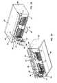
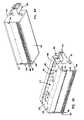
- FIGS. 1 and 2show an embodiment of a loaded chassis 100 in accordance with the present invention.
- the chassis 100includes vertical sidewalls 102 , 104 made of metal such as cold-rolled steel with a chromate plating and includes a baffle surface 112 positioned between the vertical sidewalls 102 , 104 and made of a material such as cold-rolled steel or aluminum.
- the baffle surface 112is substantially perpendicular to the plane created by either sidewall 102 , 104 .
- the solid baffle surface 112prevents heat and/or flames from passing into areas above the chassis 100 .
- a gap 121 shown in FIG. 2allows air to pass into the area above the baffle surface 112 such as for providing ventilation to areas above the chassis 100 .
- the chassis embodiment shownis equipped to house modules 116 that engage fiber optic cables 160 .
- a cable guide 120is mounted between the vertical sidewalls 102 , 104 and receives the fiber optic cables 160 that extend from the modules 116 .
- the cable guide 120has slots 144 that allow the cables 160 to enter the cable guide 120 .
- the vertical sidewalls 102 , 104have cable exit holes 145 , 146 located to the sides of the cable guide 120 that allow the fiber optic cables 160 to exit the cable guide 120 and chassis 100 .
- the cable guide 120has a cover 114 positioned over the cavity of the cable guide 120 to prevent the fiber cables 160 from protruding above the chassis 100 .
- the cover 114has a lip 115 extending from the front edge and abutting the cable guide 120 that further maintains the cover's 114 alignment with the cable guide 120 .
- the chassis embodiment shownincludes two groups of modules 116 and three empty chambers on each side of the two groups of modules 116 .
- the empty chamberspermit the chassis 100 to accommodate a certain number of modules 116 with a cumulative width significantly less than the width required of the chassis 100 for mounting in a given rack.
- the three empty chamberseach have a front cover that is flush with the faceplate 202 of the modules 116 that is made of a metal such as cold-rolled steel with a chromate plating.
- the leftmost chamberincludes front cover 107 which includes a substantially vertical portion 106 , a second portion 148 angled with respect to the vertical portion 106 , and a third portion 150 that is substantially perpendicular to the second portion 148 and angled with respect to the vertical portion 106 .
- the center chamberincludes front cover 109 which includes a substantially vertical portion 108 , a second portion 152 angled with respect to the vertical portion 108 , and a third portion 154 that is substantially perpendicular to the second portion 152 and angled with respect to the vertical portion 108 .
- the rightmost chamberincludes front cover 111 which includes a substantially vertical portion 110 , a second portion 156 angled with respect to the vertical portion 110 , and a third portion 158 that is substantially perpendicular to the second portion 156 and is angled with respect to the vertical portion 110 .
- the faceplate 202 of modules 116 of FIGS. 1 and 2has a first substantially vertical portion 206 that is aligned and flush with the first substantially vertical portion 106 , 108 , or 110 when the module 116 is fully inserted into the chassis 100 .
- the faceplate 202also has a second portion 210 angled with respect to the first substantially vertical portion 206 that is aligned and flush with the second portion 148 , 152 , or 156 when the module 116 is fully inserted into the chassis 100 .
- the faceplate 202also has a third portion 212 that is substantially perpendicular to the second portion 210 and is angled with respect to the vertical portion 206 .
- the third portion 212is aligned and flush with the third portion 150 , 154 , or 158 .
- Providing the angled second and third portions on the modules 116permit fiber optic cable connections to be provided at an angle to prevent overbending of the cables 160 .
- the angled second and third portions on the front covers 107 , 109 , and 111protect the interior of the chassis 100 and circuitry of the modules 116 by creating a seamless barrier together with the faceplate 202 of each module 116 .
- the modules 116 and faceplate 202will be discussed in more detail below.
- the chassis 100includes a horizontal surface 118 forming a bottom to the chassis 100 .
- the horizontal surface 118which may also be made of a metal such as cold-rolled steel with a chromate plating includes a first ridge 136 extending perpendicular to the plane of the vertical sidewalls 102 , 104 .
- the ridge 136is perpendicular to a horizontal longitudinal axis of the vertical sidewalls 102 , 104 that runs from the front of the chassis 100 to the rear.
- a second ridge 142that is substantially parallel to the first ridge 136 is also included in the horizontal surface 118 .
- a recessed area 140 between the first ridge 136 and second ridge 142is also included, as is a recessed area 162 between the back edge of the horizontal surface 118 and the second ridge 142 .
- the bottom horizontal surface 118may include ventilation holes to allow air to enter the interior of the chassis 100 .
- the horizontal surface 118may be made of a mesh material with densely populated openings.
- the first ridge 136has card slots 184 that receive edges of the modules 116 . Each card slot 184 is perpendicular to the first ridge 136 .
- the first ridge 136also has divider slots 186 that divider wall edges are located within.
- the second ridge 142has card slots 138 that are linear in relation to the card slots 184 of the first ridge 136 .
- the second ridge 142also has divider slots 182 that are linear in relation to the divider slots 186 located in the first ridge 136 .
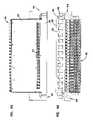
- FIG. 3shows the empty chassis 100 .
- the divider walls 128 , 130 , 132 , and 134can be seen located between card slots 138 .
- the divider walls 128 , 130 , 132 , and 134compartmentalize the interior of the chassis 100 and may be made of a material such as cold-rolled steel or aluminum. Should a fire be imposed within the interior of the chassis 100 , compartmentalization prevents the flames from spreading.
- the divider walls 128 , 130 , 132 , and 134have multiple front edges that abut the various portions of the front covers 107 , 109 , and 111 and/or various portions of the module faceplates 202 .
- the horizontal surface 118can be seen between the divider walls 128 , 130 , 132 , and 134 .
- the divider walls 128 , 130 , 132 , and 134fit into the divider slots 186 and 182 in the first ridge 136 and second ridge 142 between the card slots 138 and 184 .
- the divider walls 128 , 130 , 132 , and 134 and the divider slots 186do not extend fully across the first ridge 136 .
- the divider walls 128 , 130 , 132 , and 134abut the end of the divider slots 186 within the first ridge 136 and are held in place.
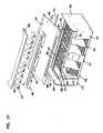
- FIG. 4shows the rear of the chassis 100 .
- the chassis 100includes a backplane 124 that is typically a printed circuit board.
- the backplanehas a plurality of coaxial input jacks 125 and output jacks 126 for sending and receiving electrical signals. The position of the jacks 125 , 126 could be swapped so that either the input or output jack is the top jack.
- a second heat baffle surface 122can also be seen.
- the second heat baffle surface 122is typically a mesh piece of metal such as aluminum having about 60% of its surface occupied by densely spaced holes.
- the second baffle surfaceacts as a flame diffuser to prevent flames that are directed out of the top of the chassis 100 from easily exiting out of the back of the heat baffle.
- the second heat baffle surface 122allows heat to be dissipated from the heat baffle.
- Ventilation holes 164 in the cable guide 120are also shown in FIG. 4 . These ventilation holes 164 allow air to pass from beyond the front of the chassis 100 through the cable guide 120 to the area above heat baffle surface 112 . The air may then rise through a ventilated bottom surface of a chassis mounted atop chassis 100 , such as when chassis are installed in a rack. This concept is shown in more detail with reference to a different chassis embodiment in FIG. 36 .
- FIG. 5shows a top view of the chassis 100 including the cable guide cover 114 and heat baffle surface 112 .
- the input coaxial jacks 125can also be seen.
- FIG. 6shows a cross-sectional front view of the cable guide 120 taken through line A-A of FIG. 5 .
- Radius limiters 166are located within the cable guide 120 and are adjacent to the cable guide slots 144 .
- the radius limiters 166have a radius that is large enough to prevent overbending of fiber optic cables 160 routed over the curved surface of the radius limiter 166 .
- Other radius limiters 190are located at the outer edges of the cable guide 120 to prevent overbending of fiber optic cables 160 as they are routed out of the cable guide and up or down the rack containing the chassis 100 .
- the cable guide 120 and cable guide cover 114may be made of a rigid material such as metal.
- the radius limiters 166 and 190may also be made of a rigid material including metal or plastic.
- the heat baffle surface 112has a front lip 180 that contains card slots 168 for receiving the edge of the modules 116 as they are inserted.
- the cable guide 120also has a rear portion with the holes 164 that allow air to pass over the region above the heat baffle surface 112 . As discussed, when chassis 100 is rack mounted, passing air into the region above the baffle surface 112 allows the air to pass into the bottom of the chassis mounted above to ventilate the circuitry contained by the modules 116 of the chassis 100 above.
- FIG. 7shows a front view of the chassis 100 .
- each cable guide slot 144is aligned with a module 116 such that the fiber optic cable 160 passes vertically from the module 116 to a cable slot 144 .
- FIG. 8shows a cross-sectional side view taken through line B-B of FIG. 7 .
- Divider wall 170located between divider walls 130 and 132 is visible in this view.
- the fiber optic cable 160passes from the angled portion 212 of the module 116 , which is flush with portion 154 of front cover 109 , up through the cable guide 120 .
- the vertical portion 108 of the front cover 109can be seen in relation to angled portion 152 and 154 .
- Angled portion 152is substantially perpendicular to angled portion 154 . As discussed below, creating the perpendicular angle on the module that is flush with angled portions 152 and 154 permit the connection axis of a fiber optic cable connector of the module 116 to be angled toward the cable guide 120 to reduce the likelihood of overbending the cables 160 .
- the top horizontal surface 172includes a recessed area 171 and a first ridge 176 extending perpendicular to the vertical sidewalls 102 , 104 and a second ridge 178 that is substantially parallel to the first ridge 176 .
- the top horizontal surface 172may be made of metal such as cold-rolled steel with a chromate plating and may contain ventilation holes as shown below for other embodiments or may be a mesh metal.
- the second baffle surface 122can also be seen in FIG. 8 extending from the first baffle surface 112 to the top horizontal surface 172 .
- FIG. 9shows a bottom view of the chassis 100 .
- the slots 144 of the cable guide 120are visible along with the card slots 138 , 184 and divider slots 182 , 186 of the bottom horizontal surface 118 .
- Also shownare the recessed areas 140 and 162 defined by the first ridge 136 and second ridge 142 .
- the divider slots 186 of the first ridge 136do not fully extend across the first ridge 136 . This enables the divider walls to fit into the divider slots 186 and be held in place so that they cannot slide out the front of the chassis 100 .
- FIG. 10shows a rear view of the chassis including the backplane 124 .
- the first baffle surface 112 and second baffle surface 122can be seen as well as the input and output coaxial connectors 125 and 126 .
- each module 116 inserted into the chassis 100becomes electrically connected to one pair of the input and output connectors 125 , 126 .
- FIG. 11shows a perspective view of the chassis 100 with an alternative module 188 being inserted.
- the alternative module 188includes a shell surrounding the circuit board of the module 188 which is discussed in more detail below with reference to FIGS. 18 and 19 .
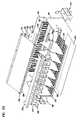
- FIG. 12shows an exploded view of the chassis 100 where the heat baffle components and cable guide components have been exploded.
- the details of the top horizontal surface 172can be seen including the first ridge 176 , second ridge 178 , and recessed area 174 between the first and second ridges 176 , 178 .
- the first and second ridges 176 , 178are parallel to each other and are perpendicular to the longitudinal axis of the vertical sidewalls 102 , 104 .
- card slots 194for receiving a top edge of the modules 116 and divider slots 192 for receiving a top edge 171 of the divider walls 128 , 130 , 132 , 170 , and 134 .
- the ridges 176 , 178allow the card slots 194 to be included while maintaining the rigidity of the top horizontal surface 172 . Rather than being included in the ridges 176 , 178 , the card slots 194 extend across the recessed area 174 but not across the ridges 176 , 178 to receive the top edge of modules 116 .
- the card slots 194 and divider slots 196are perpendicular to the ridges 176 , 178 and are aligned with the card slots 138 , 184 and divider slots 182 , 184 of the bottom horizontal surface 118 . Additionally, the lip 180 of the baffle surface 112 can be seen as can the card slots 168 of the lip 180 . The card slots 168 align with the card slots 194 of the top horizontal surface 172 to enable the modules 116 to be inserted into the chassis 100 .
- top horizontal surface 172can also be seen in FIG. 13 wherein the heat baffle and cable guide 120 have been removed.
- the divider wall 196 abutting the front cover 111can be seen as can divider walls 128 , 130 , 170 , 132 , and 134 where walls 132 and 170 abut the front cover 109 and divider wall 128 abuts front cover 107 .
- four module compartmentsare formed by the divider walls 128 , 130 , 170 , 132 , 134 , and 196 that may prevent the spread of flames should a fire be imposed.
- FIG. 14shows an exploded view of the chassis 100 including the backplane 124 and top horizontal surface 172 .
- the backplane 124includes several module connectors 198 that receive a connector of the module 116 to establish electrical continuity between the input and output coaxial connectors 125 , 126 and the circuitry of the module 116 .
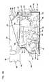
- FIG. 15shows an embodiment of a module 116 .
- the module 116includes circuitry 224 for transferring signals from an input to an output. As shown for this embodiment, the circuitry 224 for transferring signals is specifically for converting input electrical signals to output optical signals and/or for converting input optical signals to output electrical signals. The operation of the circuitry 224 is discussed below.
- the module 116includes a printed circuit board 236 having top edge 216 and bottom edge 218 that fits within the card slots of the chassis 100 previously discussed.
- the modulealso includes a cage 222 enclosing several components of the circuitry 224 to provide isolation from electromagnetic interference.
- the cage 222may be made of metal such as aluminum.
- the module 116also includes a connector 220 for engaging the backplane connector 198 previously discussed.
- a faceplate 202is included with the first vertical portion 206 , second portion 210 angled with respect to the first portion, and a third portion 212 that is perpendicular to the second portion 210 .
- the faceplate 202may be made of metal and includes a visual indication area 208 where light emitting diodes (LEDs) protrude from openings. The LEDs give an indication of the operational state of the circuitry 224 .
- the faceplate 202also includes a handle 204 that a user may grasp when inserting or removing the module 116 from a chassis 100 .
- a fiber optic cable connector 214is included and has a connection axis, which is the direction of insertion of the cables 160 , that is perpendicular to the third portion 212 and parallel to the second portion 210 .
- FIG. 16shows the opposite side of the module 116 .
- the connector 220protrudes beyond the back of the circuit board 236 .
- the faceplate 202includes mounting arms 232 and 234 .
- Mounting arm 232extends from the third portion 212 to the printed circuit board 236
- the mounting arm 234extends from the first portion 206 to the printed circuit board 236 .
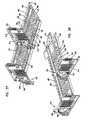
- FIG. 17shows an exploded view of the module 116 .
- the cage 222is mounted to the circuit board 236 with mount 226 .
- the fiber optic cable connector 214is mounted along a front edge 237 of the printed circuit board 236 but is angled with respect to the front edge 237 .
- the fiber optic cable connector 214includes an input connector 213 and an output connector 215 .
- the fiber optic cable connector 214protrudes through an aperture 230 in the third portion 212 of the faceplate 202 .
- FIGS. 18 and 19show an alternative module 188 .
- This module 188has a shell 236 covering the entire printed circuit board 258 .
- the shell 236may be made of a metal such as aluminum.
- the circuit board 258includes a connector 260 that protrudes from the back of the shell 236 that can be inserted into a module connector 198 of a chassis 100 .
- the shell 236includes a top surface 250 with ventilation holes 252 .
- the shell 236also includes a bottom surface 254 with ventilation holes 256 .
- the circuit board 258may mount to a side surface 266 of the shell 236 .
- the side surface 266includes top edge 248 and bottom edge 274 . These edges 248 , 274 may be positioned within card slots of the chassis 100 when the module 188 is inserted.
- the printed circuit board 258includes a front edge 259 and a fiber optic cable connector 246 is mounted along the first edge 259 .
- the fiber optic cable connector 246is mounted such that the connection axis is angled with respect to the front edge 259 so that at least a portion of the fiber optic cable connector 246 extends beyond the front edge 259 .
- the fiber optic cable connector 246includes an input connector 245 and an output connector 247 .
- module 188may contain circuitry 264 for transferring signals.
- the circuitry 264may convert electrical signals to optical signals and optical signals to electrical signals as discussed in detail below.
- the side surface 266has three portions 268 , 270 , and 272 to its front edge.
- the first portion 272is substantially vertical when installed in a chassis 100 .
- the second portion 270is angled with respect to the first portion 272 .
- the third portion 268is substantially perpendicular to the second portion 270 and is angled with respect to the first portion 272 .
- the shell 236includes a first portion 273 that is also substantially vertical when mounted in the chassis 100 as well as a second portion 271 that is angled with respect to the first portion 273 .
- a third portion 269is substantially perpendicular to the second portion 271 and angled with respect to the first portion 273 .
- a faceplate 238has a first portion 240 that is substantially vertical when installed in the chassis 240 and is parallel to the first edge 259 .
- a second portion 242is angled with respect to the first portion and is parallel to the connection axis, and a third portion 244 is substantially perpendicular to the second portion 242 and the connection axis and is angled with respect to the first portion 240 .
- the first portion 240 of the faceplate 238abuts the first portion 272 of the side surface 266 and the first portion 273 of the shell 236 .
- the second portion 242 of the faceplate 238abuts the second portion 270 of the side surface 266 and the second portion 272 of the shell 236 .
- the third portion 244 of the faceplate 238abuts the third portion 268 of the side surface 266 and the third portion 269 of the shell 236 .
- the module 188is shielded from electromagnetic noise by the enclosure formed by the intersection of the faceplate 238 , side surface 266 , and shell 236 .
- the faceplate 238includes an aperture 262 in the third portion that exposes the fiber optic cable connector 246 to allow it to receive fiber optic cables 160 .
- the faceplate 238also has a visual indication area 176 in the first portion 240 where LEDs protrude and provide an indication of the operating state of circuitry 264 .
- the shell 236may also contain a back surface (not shown) opposite the faceplate 238 that has an aperture for allowing the connector 260 to extend beyond the back surface.
- FIG. 20shows a high-level block diagram of circuitry such as that contained in module 116 of FIG. 15 or module 188 of FIG. 18 for converting electrical signals to optical and optical signals to electrical.
- the optical signalsare received by the optical to electrical circuitry 279 through fiber media 278 .
- a fiber optic receiver 280receives the optical signal and passes it to clock and data recovery circuitry 284 .
- a optical receiver loss-of-signal (LOS) circuit 282detects the signal level received by the fiber optic receiver 280 to determine whether a signal is present. If not, a minor alarm is generated whereby a visual indicator on the faceplate is triggered and an alarm signal is delivered through the backplane of the chassis to a downstream device.
- LOSoptical receiver loss-of-signal
- Clock and data recovery circuit 284 of a given data ratesuch as Digital Signal Heirarchy 3 (DS3) (44.736 Mbps) or SONET Synchronous Signal Transfer rate (STS-1) (51.840 Mbps)
- DS3Digital Signal Heirarchy 3
- STS-1SONET Synchronous Signal Transfer rate
- An electrical signal driver 286 of the particular data ratereceives the clock and data and reconstructs the electrical signal with the appropriate amplitude and shape before outputting it through an electrical conductor 290 .
- An electrical transmitter LOS circuit 288detects the signal level output by the driver 286 to determine whether the driver 286 is functioning. If not, a major alarm is generated whereby a visual indicator on the faceplate is triggered and an alarm signal is delivered through the backplane of the chassis to the downstream device.
- the electrical signalsare received through electrical conductor 304 by the electrical to optical circuitry 293 .
- a receiver circuit 300 of a given data raterecovers the clock and re-times the data prior to sending the signal to the differential driver circuit 298 .
- An electrical receiver LOS circuit 302detects the signal level received by the receiver circuit 300 to determine whether a signal is present. If not, a minor alarm is generated whereby a visual indicator on the faceplate is triggered and an alarm signal is delivered through the backplane of the chassis to a downstream device.
- a differential driver circuit 298 operating at a given data ratethen converts the data to a differential signal.
- a fiber optic transmitter 294then takes the differential signal and converts it to light pulses delivered to the optical media 292 .
- Optical transmit LOS circuit 296detects the signal level output by the optic transmitter 294 to determine whether the optic transmitter is functioning. If not, a major alarm is generated whereby a visual indicator on the faceplate is triggered and an alarm signal is delivered through the backplane of the chassis to a downstream device.
- FIG. 21shows a detailed block diagram of the circuitry 224 for converting optical signals to electrical and electrical signals to optical.
- the circuitry 224 of the block diagram of FIG. 21is configured to convert optical signals to electrical signals of two different data rates and to convert electrical signals of two different data rates to optical signals.
- a usermay selectively configure the circuitry 224 for one data rate or the other by positioning a switch to a first position to enable certain components dedicated to one data rate to function or positioning the switch to a second position to enable other components dedicated to another data rate to function.
- the circuitry 224receives an electrical signal of one of the data rates through the coaxial connector 125 of the chassis 100 previously discussed.
- the electrical signalpasses through an input isolation transformer 306 and then to a line interface unit 310 (LIU), such as the Exar XRT73L00IV or the Infineon PEB 3452-V12.
- LIUline interface unit 310
- the LIU 310is set to operate at the desired data rate and reconstructs the data signal by recovering the clock and retiming the data.
- the LIU 310typically includes an automatic gain control that changes the gain and equalization to compensate for cable losses.
- the LIU 310is set to operate at the appropriate data rate by a data rate jumper or switch 313 that is manipulated by the user. Additionally, a reference signal generator, such as the DS3 oscillator 312 and/or STS-1 oscillator 314 feeds a reference clock signal to the LIU 310 . The particular oscillator output 312 or 314 received by the LIU 310 is also controlled by user manipulation of the data rate jumper 313 .
- An exemplary oscillatoris the Mtron M8S28TCJ.
- a Pseudo Emitter Coupled Logic (PECL) differential driver 316receives a single rail non-return-to-zero (NRZ) data stream with a Low Voltage Transistor-Transistor Logic (LVTTL) level from the LIU 310 and converts this signal to a differential Low Voltage Pseudo Emitter Coupled Logic (LVPECL) signal.
- a fiber optic transmitter 318then outputs light pulses based on the differential LVPECL signal to the output optical connector 213 of the module 116 previously discussed.
- a window comparator 320is driven by an analog monitor signal provided by the fiber optic transmitter 318 to determine whether a signal is present. If not, then the window comparator 320 outputs a trigger signal to alarm circuitry 322 .
- Alarm circuitry 322then drives an LED from the set of visual indicators 324 exposed on the visual indicator area 208 of module 116 .
- Alarm circuitry 322also triggers an alarm relay 326 to send an alarm signal through contacts 238 of the backplane 124 .
- Alarm circuitry 322is generally a portion of a programmable logic device (PLD) such as the Atmel ATF1504ASV-15AI44.
- PLDprogrammable logic device
- Optical signalsare received through optical connector 215 of the module 116 .
- a fiber optic receiver 336receives the light pulses and generates an LVPECL differential signal.
- a PECL differential receiver 340takes the differential signal and generates an intermediate signal that is a single-ended LVTTL NRZ data stream. This intermediate signal is delivered to a clock and data recovery circuit 342 or 344 of the selected data rate as chosen by the position of jumper or switch 313 . As shown, the two data rates are DS3 for data recovery circuit 344 and STS-1 for data recovery circuit 342 .
- DS3for data recovery circuit 344
- STS-1for data recovery circuit 342 .
- One skilled in the artwill recognize that other data rates are possible as well.
- a PECL receiver 338detects whether the difference signal is present from the fiber optic receiver 336 and sends a signal to the alarm circuit 322 if the signal is absent.
- the alarm circuit 322then triggers the visual indicator 324 and an alarm relay 326 which then sends a signal through alarm contacts 238 of the backplane 124 .
- the outputs of the data and clock recovery circuitsare logically OR'd together through signal switching device 346 for the clock and signal switching device 348 for the data.
- the jumper or switch 313controls the switching devices 346 , 348 so that the appropriate clock and data recovery circuit 342 or 344 is in communication with the LIU 310 .
- the switching device 346feeds the clock signal to the transmit clock input of the LIU 310 .
- the switching device 348feeds the data signal to the transmit data input of the LIU 310 .
- the LIU 310reconstructs the data signal and amplifies and shapes the output data signal based on the cable to be used to transfer the electrical signal.
- the output electrical data signalis passed through isolation transformer 308 and then to the output coaxial connector 126 of the chassis 100 .
- the circuitry 224is powered by a ⁇ 48 V DC power connection 334 in the backplane 124 of the chassis 100 .
- the ⁇ 48V DC poweris supplied through the connectors 198 of the backplane 124 to the connectors 220 of the module 116 .
- the module 116may include a DC-DC converter 332 , such as the Ericsson PKF4610, that creates a 3.3 V output that is distributed to the various active components of the circuitry 224 .
- a power supply monitor 330may be included to detect whether the DC-DC converter 332 is providing the appropriate voltage and may send a signal to trigger the alarm circuit 322 if the voltage is not correct.
- the alarm circuitry 322may then trigger a relay 326 to activate a visual indicator 324 and a major alarm signal through a backplane contact 238 .
- the fiber optic transmitter 318 and receiver 336may be combined along with the window comparator 320 and PECL receiver 338 into one unit such as the OCP DTR-052-3.3-SM2-A-L3 or Excelight SCM7591XC-W optical transceiver that also includes the PECL differential driver 316 and PECL differential receiver 340 .
- the clock and data recovery circuits 342 , 344may be the Vectron TRUOIO-GKLGB or Micrel SY87700LHI.
- FIG. 22shows a first alternative embodiment of a loaded chassis 350 made of materials such as those discussed with reference to the chassis 100 of FIG. 1 .
- This chassis 350is configured to utilize all of its width to accommodate modules 116 . As shown, the embodiment of FIG. 22 holds twice as many modules 116 as the chassis 100 of FIG. 1 .
- the chassis 350includes a right vertical sidewall 352 and a left vertical sidewall 354 .
- a heat baffle surface 356is also included between the vertical sidewalls 352 , 354 .
- a cable guide 368is also included between the vertical sidewalls 352 , 354 .
- the cable guide 368includes several alternative radius limiters 362 for preventing overbending of fiber cables 160 .
- the radius limiter 362includes a vertically oriented arch 364 adjacent to each cable slot 365 and a horizontally oriented arch 366 placed above and between each vertically oriented arch 364 . The cables may then pass beside the vertically oriented arch 364 and above the horizontally oriented arch 366 until exiting out an exit opening 353 formed by the sidewall 352 or 354 and a cable guide cover 358 .
- the cable guide cover 358may contain rear downward extensions 357 defining a plurality of open areas 359 .
- the open areas 359allow air to penetrate through the cable guide 368 and enter the area above the heat baffle surface 356 . As before, this enables the area above the heat baffle surface 356 , such as another chassis mounted in a rack, to be ventilated.
- the bottom horizontal surface 361 of this embodimentincludes at least one ridge 360 .
- the ridge 360may include card slots 363 for receiving edges of the modules 116 .
- the chassis 350may also include a top horizontal surface (not shown) like that of the previously discussed embodiment shown in FIG. 12 .
- the top horizontal surfacemay also contain card slots for receiving a top edge of modules 116 .
- Both the top horizontal surface and the bottom horizontal surface 361may contain ventilation holes between card slots, as shown below with reference to additional embodiments, or may be made of a mesh material with densely spaced holes.
- FIGS. 23 and 24are perspective front views of a loaded chassis 400 of a second alternative embodiment.
- This embodiment of the chassis 400contains spacing like that of the embodiment of FIG. 1 so that the total width of the chassis 400 is significantly greater than the cumulative widths of the modules 422 that it contains thereby allowing the chassis 400 to fit within a given rack size.
- the chassis 400includes right and left vertical sidewalls 402 , 404 that may be made of a metal such as cold-rolled steel with a chromate plating.
- the vertical sidewalls 402 , 404have portions 412 , 416 that form front panels of the chassis 400 .
- Another front panel 414 of the same materialis also included and has three distinct portions.
- a first substantially vertical portion 418forms the bottom.
- a second portion 420is angled with respect to the first portion 418 .
- a third portion 444is substantially vertical and lies in a different plane than the first portion 418 .
- the front panel 414is flush with a faceplate 424 of modules 422 mounted within the chassis 400 .
- the faceplate 424has three portions including a first substantially vertical portion 426 that is aligned and flush with the first portion 418 of the front panel 414 .
- the faceplate 424also has a second portion 428 that is angled with respect to the first portion 418 and aligned and flush with the second portion 420 of the front panel 414 .
- the faceplate 424additionally has a third portion 430 that is substantially vertical but lies within a different plane from the first portion 426 and that is aligned and flush with the third portion 444 of the front panel 414 .
- the faceplate 424 and front panel 414together create a seamless front surface to the chassis 400 thereby protecting the interior region and circuitry housed by modules 422 .
- the chassis 400also includes a baffle surface 436 disposed between the vertical sidewalls 402 , 404 that is a solid metal such as cold-rolled steel or aluminum.
- a cable guide 406is also included and mounts to the vertical sidewalls 402 , 404 .
- the cable guide 406includes several cable slots 434 and radius limiters 410 adjacent to each cable slot.
- a cable guide cover 408is mounted atop the cable guide 406 .
- the cable guide cover 408has vertical extensions 440 aligned with each cable slot 434 .
- the cable guide 406includes vertical extensions 472 that coincide with each radius limiter 410 and are spaced between each vertical extension 440 of the cover 408 .
- the vertical extensions 472 and 440maintain fiber cables within the cable guide 406 while the allowing air to penetrate the cable guide 406 .
- the second portion 428 of each faceplate 424has a fiber optic cable connector 432 angled toward the cable guide 406 to reduce the bending of fiber cables passing from the module 422 to the cable guide 406 .
- a separation 442exists between the cable guide 406 and the third portion 430 of the modules and third portion 444 of the front panel 414 .
- This separation 442allows air to pass into the area above the heat baffle surface 436 to ventilate the area above the heat baffle surface 436 .
- the separation 442 of this embodimentis expanded to provide further ventilation due to the setback of the second and third portions 428 , 430 of the modules 422 and second and third portions 420 , 444 of the front panel 414 .
- the bottom-most horizontal surface 438 of the chassis 400may be made of a metal mesh material such as aluminum with densely spaced holes throughout. As discussed below, the surface 438 underlays an additional horizontal bottom surface with structures for supporting the modules 422 and for providing ventilation to the interior of the chassis 400 .
- FIGS. 25 and 26are front and rear perspective views of an empty chassis 400 of the second alternative embodiment.
- a horizontal bottom surface 476can be seen and may be made of a metal such as cold-rolled steel with a chromate plating.
- the horizontal surface 476has a first ridge 454 that includes card slots 458 and ventilation holes 456 between each adjacent pair of card slots 458 .
- the chassis 400is compartmentalized by installation of divider walls 445 , 446 , and 447 .
- Each divider wall 445 , 446 , and 447has a front edge with three distinct portions including a bottom substantially vertical first portion 448 , a second portion 450 angled with respect to the first portion 448 , and a substantially vertical third portion 452 set-back from the first portion 448 .
- the divider walls 445 , 446 , and 447fit within divider slots in the first ridge 456 which are discussed in more detail below.
- the cable guide cover 408includes vertical extensions 460 on the rear side of the cover 408 . These extensions 460 permit air to flow through the rear of the cover 408 while preventing fiber cables from escaping.
- the heat baffleincludes heat baffle surface 462 which extends from the first baffle surface 436 toward a backplane 464 .
- the heat baffle surface 462is typically a metal mesh material that diffuses flames but allows hot air to pass through.
- the first heat baffle surface 436is generally solid metal to prevent hot air and flames from rising into areas above the chassis 400 .
- the backplane 464 of the chassis 400is typically a printed circuit board that establishes electrical connection between the input and output coaxial connectors 466 and 470 and a backplane connector discussed below that interfaces with a connector on the modules 422 .
- Conductive pins and/or circuit tracesmay be exposed on the backplane 464 so a lexan cover 468 is placed over the vulnerable areas of the backplane 464 .
- FIG. 27shows a top view of the second alternative chassis 400 .
- the orientation of the cable guide cover 408 , first heat baffle surface 436 , modules 422 , and front panel 414can be seen.
- the opening 442 over the modules 422 and front panel 414allows air to be circulated beyond the cable guide 406 and cover 408 and the first heat baffle surface 436 directs it into the area above the chassis 400 .
- FIG. 28shows a front cross-sectional view taken through line A-A of FIG. 27 .
- the cable guides 410are visible along with the modules 422 and front panel 414 .
- the rear portion of the cable guide 406can be seen in relation to the rear vertical extensions 460 that allow air to pass through the rear of the cable guide 406 to the first baffle surface 436 .
- FIG. 29is a front view of the chassis 400 which shows the alignment of the modules 422 relative to the cable slots 434 and vertical extensions 470 and 440 .
- the cable slots 434are positioned such that two modules 422 lie beneath each cable slot 434 allowing fiber cables to pass directly from the modules 422 to the cable guide 406 through the cables slots 434 .
- FIG. 30is a side view taken through line B-B of FIG. 29 . The orientation of the fiber optic cable connector 432 relative to the cable guide 406 can be seen.
- the angled second portion 420 of the front panel 414is flush with the second portion 428 , and the connection axis of the fiber optic cable connector 432 is directed at the cable guide 406 to minimize the bending of the fiber cables.
- the heat baffle surfacesare also visible in FIG. 30 .
- the first heat baffle surface 436is angled with respect to the horizontal surfaces of the chassis 400 and is perpendicular to the plane of the vertical sidewalls 402 , 404 .
- the second heat baffle surface 462is angled with respect to the horizontal surfaces, also angled with respect to the first heat baffle surface 436 , and is perpendicular to the plane of the vertical sidewalls 402 , 404 .
- This embodimentalso includes a third heat baffle surface 474 that lies within a plane parallel to the second heat baffle surface 462 , with a separation 461 existing between the second 462 and third 474 heat baffle surfaces.
- Both the second 462 and third 474 heat baffle surfacesmay be made of a mesh metal material such as aluminum with densely spaced holes which act as a flame diffuser while allowing hot air to escape.
- the separation 461further enhances the diffusive character of the heat baffle surfaces 462 , 474 .
- FIG. 31is an exploded perspective view of the chassis 400 .
- a top horizontal surface 478can be seen which underlies the heat baffle surfaces 436 , 462 , and 474 .
- the top horizontal surface 478includes a first ridge 480 and a second ridge 482 and may be made of metal such as cold-rolled steel with a chromate plating.
- a recessed area 481lies between the ridges 480 , 482 and has card slots 486 and divider wall slots 484 .
- the card slots 486receive top edges of modules 422
- the divider slots 484receive top edges of divider walls 446 .
- Ventilation holes 492are provided between each adjacent pair of card slots 484 .
- the ventilation holes 492allow hot air to rise out of the interior region of the chassis 400 and escape through the exit of the heat baffle formed by surfaces 462 and 474 .
- a lip 488 of the heat baffle surface 436hangs below and in front of the top horizontal surface 478 and receives the faceplate 424 of the modules 422 .
- the lip 488has card slots 490 that align with the card slots 484 of the top horizontal surface 478 to allow the top edge of the modules 422 to slide into the interior region of the chassis.
- the ridges 480 and 482 of the top horizontal surface 478allow the card slots 486 and divider slots 484 to extend fully across the recessed area 491 while maintaining rigidity of the surface 478 .
- the vertical sidewalls 402 , 404have, in addition to the front panel portions 412 and 416 , interior side extensions 417 and 413 formed by further bending of the metal making up the sidewalls 402 , 404 .
- the interior side extensions 417 and 413abut all three portions 426 , 428 , and 430 of the faceplate 424 of the modules 422 that are mounted on each end so as to create a seamless barrier at the front of the chassis 400 .
- FIG. 32shows a rear perspective view of the chassis 400 with the heat baffle surfaces and cable guide surfaces removed.
- FIG. 33is an exploded view of the chassis 400 without the heat baffle surfaces and cable guide surfaces.
- the details of the inner side of the backplane 464are visible, including backplane connectors 490 that engage connectors of the modules 422 when they are fully installed in the chassis 400 .
- the details of the bottom horizontal surface 476are also visible, including the first ridge 454 , a second ridge 488 , and a recessed area 499 defined by the first and second ridges 454 , 488 .
- the first ridgehas card slots 458 and divider slots not seen in this view. Ventilation holes 456 are provided between each adjacent card slot 458 within the first ridge 454 .
- Ventilation holes 494are provided within the recessed area 499 . Ventilation holes 496 are also provided between adjacent card slots 459 of the second ridge 488 . The second ridge 488 and the back edge of horizontal surface 476 define a recessed area 497 that includes ventilation holes 498 .
- FIG. 34shows a front view of the chassis 400 with bracket structures 504 , 506 that also serve as vertical cable guides.
- the bracket structures 504 , 506include a bracket portion 500 , 502 that abuts a rail of a rack (not shown).
- the bracket portion 500 , 502is fastened to the rail to mount the chassis 400 within the rack.
- the cable guide portion 501 , 503 of the bracket structures 504 , 506restricts the fiber cables 508 exiting the cable guide 406 .
- the fiber cables 508 from each chassis 400 in the rackpass through subsequent cable guide portions 501 , 503 of adjacent chassis until the cables 508 reach a splice tray (not shown) at the top or bottom of the rack.
- the fiber cables 508extend from the modules 422 up though the cable slots 434 formed by vertical extensions 472 of the cable guide 406 .
- the fiber cables 508pass over the radius limiters 410 and pass out the side of the cable guide 406 over an additional radius limiter 410 at the edge of the chassis 400 . From the radius limiter 410 at the edge of the chassis 400 , the fiber cables 508 pass down through the cable guide portions 501 or 503 of the bracket structure 502 or 504 .
- FIG. 35is a right-side view of the chassis 400 with the right vertical sidewall 402 removed.
- a surface of a shielding cage 514has also been removed to reveal additional circuitry 512 that lies beneath the cage 514 on a circuit board 520 of each module 422 .
- the cage 514 and circuitry 512 beneath itlie directly over the recessed area 499 between the first ridge 454 and second ridge 488 of the bottom horizontal surface 476 .
- the circuit board 520also includes a fiber optic transceiver 510 that is positioned directly above the first ridge 454 .
- a DC-DC converter 516is also included on the circuit board 520 and is positioned directly above the second ridge 488 .
- the openings 456 and 496 within the first and second ridges 454 , 488permit air to circulate passed the fiber optic transceiver 510 and DC-DC converter 516 , while ventilation holes 494 in the recessed area 499 allows air to circulate over the circuitry 512 .
- Airis also circulated by the module 422 and through the ventilation holes 492 in the top horizontal surface 478 .
- the modules 422produce heat that is dissipated into the air and causes the air to warm and rise.
- the airmay then exit out of the chassis 400 by passing beneath baffle surface 436 and out through additional baffle surfaces 462 and 474 .
- the flamesmay rise through the ventilation holes 492 in the top horizontal surface 478 and the flames are directed by the baffle surface 436 toward baffles surface 474 .
- the mesh material of surface 474diffuses the flames, as does separation 461 and the mesh material of surface 462 .
- a connector 518 of the module 422engages backplane connector 490 . Electrical continuity is then established between the module 422 and the input and output coaxial connectors 466 , 470 on the backplane 464 .
- FIG. 36is a cross-sectional view of two stacked chassis 400 , 401 , such as through line B-B of FIG. 29 , as they would be appear while mounted in a rack.
- Air that enters the bottom chassis 400 through the cable guide 406 and through the gap 442 provided between the cable guide 406 and modules 422 and front panel 414passes into the area above the heat baffle surface 436 .
- the airis then directed by the heat baffle surface 436 into the bottom horizontal surface 438 ′ of the chassis 401 stacked atop chassis 400 .
- the bottom horizontal surface 438 ′is a ventilated surface such as a mesh metal with densely populated holes that allow the air to pass through.
- the airthen passes by the modules 422 ′ and out of the chassis 401 through the heat baffle surfaces.
- FIG. 37shows the module 422 mounted in relation to the bottom horizontal surface 476 . Also visible in this view are divider wall slots 455 in the first ridge 454 and divider wall slots 457 in the second ridge 488 that receive the bottom edge of the divider walls 446 . A bottom edge 522 of the circuit board 520 of the module 422 is disposed within the card slots 458 in the first ridge 454 and card slots 459 in the second ridge 488 .
- the fiber optic transceiver 510is located directly over the ventilation hole 456 of the first ridge 454 .
- the shielding cage 514is located directly over the ventilation holes 494 of the recessed area 499 .
- the DC-DC converter 516is located directly over the ventilation holes 496 of the second ridge 488 .
- FIG. 38shows the module 422 mounted in relation to the top horizontal surface 478 and heat baffle surface 436 .
- a top edge 524 of the circuit board 520is disposed in the card slot 490 in the lip 480 of the baffle surface 436 .
- the top edge 524 of the circuit board 520is also disposed in the card slot 486 of the recessed area 471 of the top horizontal surface 478 .
- the shielding cage 514 and the DC-DC converter 516are positioned directly under the ventilation holes 492 of the recessed area 471 .
- FIG. 39shows an exploded view of the module 422 .
- the module 422includes the fiber optic cable connector 432 with the input connector 508 and output connector 509 .
- the module 422has the connector 518 mounted along a back edge 534 of the circuit board 520 .
- the faceplate 424mounts along three portions 528 , 530 , and 532 of the front edge of the circuit board 520 .
- the bottom vertical portion 426 of the faceplate 424mounts adjacent to a first vertical portion 528 of the front edge of the circuit board 520 .
- the second portion 526 of the faceplate 424mounts adjacent to a second portion 530 of the front edge of the circuit board 520 .
- the second portion 530is angled with respect to the first vertical portion 528 .
- the third portion 430 of the faceplate 424mounts adjacent to a third vertical portion 532 of the front edge of the circuit board 520 that is set back from the first vertical portion 528 .
- the faceplate 424may also have a handle portion 538 .
- the second portion 424 of the faceplate 424has an aperture 526 that exposes the input 508 and output 509 connections of the fiber optic cable connector 432 .
- the fiber optic cable connector 432has a connection axis that is perpendicular to the second portion 530 of the front edge of the printed circuit board 520 .
- the faceplate 424includes a fastener 540 that may attach to the lip 488 of the baffle surface 436 of the chassis 400 .
- the module 422also includes visual indicator LEDs 536 that provide the visual indication of the module's operation.
- FIG. 40is a bottom front perspective view of a third alternative embodiment.
- the chassis 600 of FIG. 40is configured to hold modules throughout the area between vertical sidewalls 602 and 604 .
- the chassis 400 shown in FIG. 40is empty but has covers 614 mounted in place of modules.
- the covers 614isolate the interior when modules are not installed and include a first vertical portion 626 , a second portion 628 angled with respect to the first vertical portion 626 , and a third vertical portion 630 set back from the first vertical portion 626 .
- the chassis 600includes a cable guide 606 having vertical extensions 626 separated to form cable slots 625 .
- a radius limiter 610lies between each cable slot 625 .
- a cable guide cover 608is also included and has vertical extensions 624 offset from the vertical extensions 626 .
- a gap 612is provided between the modules or covers 614 and the cable guide to permit air to pass into the area above the chassis 600 . Air may also pass horizontally through cable guide 606 to reach the area above the chassis 600 .
- the chassis 600has bracket structures 618 , 620 that allow the chassis 600 to be mounted to a rack while guiding cables passing vertically from the chassis 600 .
- Vertical cable guide portions 617 and 621restrict the cable.
- Bracket portion 619abuts the rail of a rack (not shown) and is mounted to the rail to hold the chassis 600 within the rack.
- the chassis 600may also include a bottom horizontal surface 616 that may be made of a metal mesh such as aluminum with densely populated openings that allow air to pass through. As shown in FIG. 41 , the chassis 600 includes a heat baffle surface 622 disposed between the sidewalls 602 , 604 .
- FIGS. 42 and 43show a perspective view of the chassis 600 filed with modules 632 .
- Modules 632include a faceplate with three portions including a vertical portion 634 , a second portion 636 , and a third vertical portion 638 .
- a fiber optic cable connector 640is present at the second portion 636 .
- Module 632may be the same as module 422 shown in FIG. 39 .
- FIG. 44shows a bottom rear perspective view of the chassis 600 .
- the chassis 600includes a second heat baffle surface 642 that extends vertically between the heat baffle surface 622 and a backplane 646 .
- the backplane 646has input and output coaxial connectors 648 and 650 .
- a lexan cover 644may cover vulnerable portions of the backplane 646 wherein conductors are exposed.
- Chassis ground connections 654may also be provided to establish a chassis ground connection for the circuitry of the modules 632 .
- FIG. 45is a top rear perspective view of the chassis 600 .
- the gap 612 between the heat baffle surface 622 and the cable guide 606can be seen.
- the cable guideincludes a rear vertical portion 652 defining ventilation slots 651 that allow air to pass through the cable guide 606 .
- FIG. 46shows a front view of the empty chassis 600 .
- FIG. 47shows a top view of the empty chassis 600 .
- FIG. 48shows a right side view of the empty chassis 600 .
- radius limiters 610are provided over the bracket structure 618 , 620 to prevent overbending of cables as they are directed down through the bracket structure 618 , 620 from the cable guide 606 .
- the bracket structure 618 , 620extends forward from the sidewalls to underlay the cable guide 606 .
- FIG. 49shows a front view of the loaded chassis 600
- FIG. 50shows a top view of the loaded chassis 600
- FIG. 51shows a right side view of the loaded chassis 600 with the right side panel 602 removed.
- Modules 632may include a fiber optic transceiver 711 , a cage 710 covering media conversion circuitry, and a DC-DC converter 712 .
- the fiber optic transceiver 711lies over a first ridge 668 of the bottom surface 666 .
- the cage 710lies between the first ridge 668 and a second ridge 670 of the bottom surface 666 .
- the DC-DC converter 712lies above the second ridge 670 .
- a U-shaped channel 698passes horizontal over the modules 632 and between the sidewalls 602 , 604 .
- the U-shaped channel 698includes card slots discussed below that receive a top edge of the module 632 to guide it as it is inserted into the chassis 600 .
- FIG. 52shows an exploded view of the chassis 600 with the cable guide 606 and associated structures removed.
- the heat baffle surface 622has a lip 656 that has card slots 658 for receiving a top edge of the modules 632 .
- a third heat baffle surface 660may also be included and is spaced from the heat baffle surface 642 by separation 662 . Projections 702 may be included to maintain the separation 662 .
- the heat baffle surface 642 and surface 660may be a metal mesh material such as aluminum with densely populated openings. Furthermore, the baffle surfaces 642 and 660 may be one continuous piece of metal bent into a U shape.
- the chassis 600includes a horizontal channel 698 that extends between the two sidewalls 602 , 604 .
- the horizontal channel 698may be a metal such as cold-rolled steel or aluminum.
- the horizontal channel 698includes horizontal card slots 700 that extend parallel to the plane of the sidewalls 602 , 604 . As shown in FIG. 54 , a top edge 704 of the modules 632 is disposed within the card slots 700 .
- the chassis 600also includes a horizontal surface 666 that includes a first ridge 668 and a second ridge 670 .
- a recessed area 680is located between the first ridge 668 and the second ridge 670 .
- the second ridge 678 and the back edge of the horizontal surface 666define another recessed area 684 that includes openings 686 .
- the first ridge 668includes card slots 674 and ventilation holes 672 between each adjacent pair of card slots 674 .
- Recessed area 680includes ventilation holes 682 .
- the second ridge 670includes card slots 676 and ventilation holes 678 between each adjacent pair of card slots 676 .
- the modules 632have a bottom edge 706 that fits within the card slot 674 of the first ridge 668 and card slot 676 of the second ridge 670 .
- the module 632also includes the cage 710 covering circuitry, the DC-DC converter 712 , and the fiber optic transceiver 711 . As was discussed with reference to FIG. 51 , when the module 632 is fully installed in the chassis 600 , the cage 710 lies between the first ridge 668 and second ridge 670 and above the recessed area 680 and openings 682 . The DC-DC converter 712 lies over the second ridge 670 and opening 678 . The fiber optic transceiver 711 lies over the first ridge 668 and opening 672 .
- the module 632also includes a connector 714 on the back edge that engages the connector 664 of the backplane 646 .
- divider walls 688are included in the chassis 600 to compartmentalize the chassis 600 .
- the divider walls 688fit within divider slots 707 of the first ridge 668 and divider slots 708 of the second ridge 670 that are visible in FIG. 55 .
- the divider walls 688include a vertical edge 690 , a vertical edge 694 set back from the vertical edge 690 , an angled edge 692 interconnected the vertical edges 690 , 694 , and another angled edge 696 that is parallel to the heat baffle surface 622 .
- a backplane 646is included at the rear of the chassis 600 and includes connectors 664 for mating to modules 632 .
- the mesh heat baffle surfaces 642 , 660span a gap between the top of the backplane 646 and the solid heat baffle surface 622 .
- the mesh heat baffle surfaces 642 , 660connect to the backplane 646 through a U-shaped channel 722 and connect to the solid baffle surface 622 through an L-shaped bar 720 .
- the mesh bottom surface 616underlays the bottom surface 666 . In this embodiment, no top horizontal surface is included so that increased ventilation out of the heat baffle is provided for the increased density of modules 632 .
- FIG. 56shows a detailed block diagram of alternative media conversion circuitry 724 that operates at multiple data rates. As shown, three data rates are selectable including DS3, STS-1, and European (E3) (34.368 Mbps). Other data rates are possible as well.
- the alternative circuitry 724includes most of the circuitry included in the previous embodiment of FIG.
- This embodimentalso includes a single oscillator 774 rather than multiple ones as previously discussed.
- a clock generator 722such as the Cypress CY2908F7I employing a phase locked loop is used to selectively generate the frequency corresponding to the desired data rate to be converted.
- the oscillator 774supplies a reference signal to the clock generator 722 .
- the clock generator 772supplies the reference frequency to the LIU 730 and a clock and data recovery circuit 764 such as the Micrel SY87700LHI.
- a switch 776 that is user manipulatedis connected to the LIU and clock generator 772 to set the data rate of the conversion.
- This embodimentalso employs a scrambler 732 and a descrambler 766 .
- the scrambler 732employs a scheme to create sufficient transitions in the TTL stream so that the clock is always recoverable, even when the NRZ data is a continuous stream of ones or zeros. Thus, the scrambler 732 effectively scrambles the signal by creating the transitions.
- the scrambler 732receives the TTL NRZ signal from the LIU 730 and feeds the scrambled TTL signal to the PECL differential driver 734 .
- the descrambler 766recovers the NRZ data from a scrambled TTL signal produced by the clock and data recovery circuit 764 .
- the descrambler 766feeds the descrambled TTL NRZ signal to the LIU 730 .
- the scrambler 732 and descrambler 766may be included as part of the functionality of the PLD, such as the Atmel ATF1504ASV-15AI44, that also performed the alarm generation.
Landscapes
- Physics & Mathematics (AREA)
- General Physics & Mathematics (AREA)
- Optics & Photonics (AREA)
- Engineering & Computer Science (AREA)
- Microelectronics & Electronic Packaging (AREA)
- Light Guides In General And Applications Therefor (AREA)
- Optical Couplings Of Light Guides (AREA)
- Insertion, Bundling And Securing Of Wires For Electric Apparatuses (AREA)
- Mounting Of Printed Circuit Boards And The Like (AREA)
Abstract
Description
Claims (26)
Priority Applications (1)
| Application Number | Priority Date | Filing Date | Title |
|---|---|---|---|
| US11/000,363US7668430B2 (en) | 2001-06-04 | 2004-11-29 | Telecommunications chassis and module |
Applications Claiming Priority (2)
| Application Number | Priority Date | Filing Date | Title |
|---|---|---|---|
| US09/873,763US6824312B2 (en) | 2001-06-04 | 2001-06-04 | Telecommunications chassis and module |
| US11/000,363US7668430B2 (en) | 2001-06-04 | 2004-11-29 | Telecommunications chassis and module |
Related Parent Applications (1)
| Application Number | Title | Priority Date | Filing Date |
|---|---|---|---|
| US09/873,763ContinuationUS6824312B2 (en) | 2001-06-04 | 2001-06-04 | Telecommunications chassis and module |
Publications (2)
| Publication Number | Publication Date |
|---|---|
| US20050135770A1 US20050135770A1 (en) | 2005-06-23 |
| US7668430B2true US7668430B2 (en) | 2010-02-23 |
Family
ID=25362263
Family Applications (2)
| Application Number | Title | Priority Date | Filing Date |
|---|---|---|---|
| US09/873,763Expired - LifetimeUS6824312B2 (en) | 2001-06-04 | 2001-06-04 | Telecommunications chassis and module |
| US11/000,363Expired - LifetimeUS7668430B2 (en) | 2001-06-04 | 2004-11-29 | Telecommunications chassis and module |
Family Applications Before (1)
| Application Number | Title | Priority Date | Filing Date |
|---|---|---|---|
| US09/873,763Expired - LifetimeUS6824312B2 (en) | 2001-06-04 | 2001-06-04 | Telecommunications chassis and module |
Country Status (3)
| Country | Link |
|---|---|
| US (2) | US6824312B2 (en) |
| AU (1) | AU2002309889A1 (en) |
| WO (1) | WO2002100144A2 (en) |
Cited By (41)
| Publication number | Priority date | Publication date | Assignee | Title |
|---|---|---|---|---|
| US20100220967A1 (en)* | 2009-02-27 | 2010-09-02 | Cooke Terry L | Hinged Fiber Optic Module Housing and Module |
| US20100296791A1 (en)* | 2009-05-21 | 2010-11-25 | Elli Makrides-Saravanos | Fiber Optic Equipment Guides and Rails Configured with Stopping Position(s), and Related Equipment and Methods |
| US7856166B2 (en) | 2008-09-02 | 2010-12-21 | Corning Cable Systems Llc | High-density patch-panel assemblies for optical fiber telecommunications |
| US20110299266A1 (en)* | 2010-06-02 | 2011-12-08 | Tyco Electronics Corporation | Aggregator for a switch rack system |
| US8433171B2 (en) | 2009-06-19 | 2013-04-30 | Corning Cable Systems Llc | High fiber optic cable packing density apparatus |
| US8542973B2 (en) | 2010-04-23 | 2013-09-24 | Ccs Technology, Inc. | Fiber optic distribution device |
| US8593828B2 (en) | 2010-02-04 | 2013-11-26 | Corning Cable Systems Llc | Communications equipment housings, assemblies, and related alignment features and methods |
| US8625950B2 (en) | 2009-12-18 | 2014-01-07 | Corning Cable Systems Llc | Rotary locking apparatus for fiber optic equipment trays and related methods |
| US8660397B2 (en) | 2010-04-30 | 2014-02-25 | Corning Cable Systems Llc | Multi-layer module |
| US8662760B2 (en) | 2010-10-29 | 2014-03-04 | Corning Cable Systems Llc | Fiber optic connector employing optical fiber guide member |
| US8699838B2 (en) | 2009-05-14 | 2014-04-15 | Ccs Technology, Inc. | Fiber optic furcation module |
| US8705926B2 (en) | 2010-04-30 | 2014-04-22 | Corning Optical Communications LLC | Fiber optic housings having a removable top, and related components and methods |
| US8712206B2 (en) | 2009-06-19 | 2014-04-29 | Corning Cable Systems Llc | High-density fiber optic modules and module housings and related equipment |
| US8718436B2 (en) | 2010-08-30 | 2014-05-06 | Corning Cable Systems Llc | Methods, apparatuses for providing secure fiber optic connections |
| US8873579B1 (en)* | 2011-09-29 | 2014-10-28 | Marvell International Ltd. | Multi-rate media independent interface over a physical coding sublayer |
| US8879881B2 (en) | 2010-04-30 | 2014-11-04 | Corning Cable Systems Llc | Rotatable routing guide and assembly |
| US8913866B2 (en) | 2010-03-26 | 2014-12-16 | Corning Cable Systems Llc | Movable adapter panel |
| US8953924B2 (en) | 2011-09-02 | 2015-02-10 | Corning Cable Systems Llc | Removable strain relief brackets for securing fiber optic cables and/or optical fibers to fiber optic equipment, and related assemblies and methods |
| US20150070819A1 (en)* | 2013-09-09 | 2015-03-12 | Acbel Polytech Inc. | Server power supply system |
| US8985862B2 (en) | 2013-02-28 | 2015-03-24 | Corning Cable Systems Llc | High-density multi-fiber adapter housings |
| US8989547B2 (en) | 2011-06-30 | 2015-03-24 | Corning Cable Systems Llc | Fiber optic equipment assemblies employing non-U-width-sized housings and related methods |
| US8995812B2 (en) | 2012-10-26 | 2015-03-31 | Ccs Technology, Inc. | Fiber optic management unit and fiber optic distribution device |
| US9008485B2 (en) | 2011-05-09 | 2015-04-14 | Corning Cable Systems Llc | Attachment mechanisms employed to attach a rear housing section to a fiber optic housing, and related assemblies and methods |
| US9020320B2 (en) | 2008-08-29 | 2015-04-28 | Corning Cable Systems Llc | High density and bandwidth fiber optic apparatuses and related equipment and methods |
| US9022814B2 (en) | 2010-04-16 | 2015-05-05 | Ccs Technology, Inc. | Sealing and strain relief device for data cables |
| US9042702B2 (en) | 2012-09-18 | 2015-05-26 | Corning Cable Systems Llc | Platforms and systems for fiber optic cable attachment |
| US9038832B2 (en) | 2011-11-30 | 2015-05-26 | Corning Cable Systems Llc | Adapter panel support assembly |
| US9059578B2 (en) | 2009-02-24 | 2015-06-16 | Ccs Technology, Inc. | Holding device for a cable or an assembly for use with a cable |
| US9075216B2 (en) | 2009-05-21 | 2015-07-07 | Corning Cable Systems Llc | Fiber optic housings configured to accommodate fiber optic modules/cassettes and fiber optic panels, and related components and methods |
| US9075217B2 (en) | 2010-04-30 | 2015-07-07 | Corning Cable Systems Llc | Apparatuses and related components and methods for expanding capacity of fiber optic housings |
| US9116324B2 (en) | 2010-10-29 | 2015-08-25 | Corning Cable Systems Llc | Stacked fiber optic modules and fiber optic equipment configured to support stacked fiber optic modules |
| US9213161B2 (en) | 2010-11-05 | 2015-12-15 | Corning Cable Systems Llc | Fiber body holder and strain relief device |
| US9250409B2 (en) | 2012-07-02 | 2016-02-02 | Corning Cable Systems Llc | Fiber-optic-module trays and drawers for fiber-optic equipment |
| US9279951B2 (en) | 2010-10-27 | 2016-03-08 | Corning Cable Systems Llc | Fiber optic module for limited space applications having a partially sealed module sub-assembly |
| US9519118B2 (en) | 2010-04-30 | 2016-12-13 | Corning Optical Communications LLC | Removable fiber management sections for fiber optic housings, and related components and methods |
| US9632270B2 (en) | 2010-04-30 | 2017-04-25 | Corning Optical Communications LLC | Fiber optic housings configured for tool-less assembly, and related components and methods |
| US9645317B2 (en) | 2011-02-02 | 2017-05-09 | Corning Optical Communications LLC | Optical backplane extension modules, and related assemblies suitable for establishing optical connections to information processing modules disposed in equipment racks |
| US9720195B2 (en) | 2010-04-30 | 2017-08-01 | Corning Optical Communications LLC | Apparatuses and related components and methods for attachment and release of fiber optic housings to and from an equipment rack |
| US9885845B2 (en)* | 2015-01-15 | 2018-02-06 | Commscope, Inc. Of North Carolina | Module and assembly for fiber optic interconnections |
| US10094996B2 (en) | 2008-08-29 | 2018-10-09 | Corning Optical Communications, Llc | Independently translatable modules and fiber optic equipment trays in fiber optic equipment |
| US11294136B2 (en) | 2008-08-29 | 2022-04-05 | Corning Optical Communications LLC | High density and bandwidth fiber optic apparatuses and related equipment and methods |
Families Citing this family (91)
| Publication number | Priority date | Publication date | Assignee | Title |
|---|---|---|---|---|
| US6824312B2 (en)* | 2001-06-04 | 2004-11-30 | Adc Telecommunications, Inc. | Telecommunications chassis and module |
| US7110527B2 (en)* | 2001-12-04 | 2006-09-19 | Adc Telecommunications, Inc. | Housing for telecommunications equipment |
| US20040017992A1 (en)* | 2002-07-26 | 2004-01-29 | Freddie Lin | Fiber optic link platform |
| US7108559B2 (en)* | 2002-08-23 | 2006-09-19 | Cisco Technology, Inc. | Router with field replaceable motherboard |
| US6912349B2 (en)* | 2002-10-08 | 2005-06-28 | Adc Telecommunications, Inc. | Wall mount chassis |
| US7636506B2 (en)* | 2003-05-13 | 2009-12-22 | Alcatel-Lucent Usa Inc. | Optical fiber management in a chassis-based network system |
| US6868219B2 (en) | 2003-05-30 | 2005-03-15 | Hubbell Incorporated | SONET multiplexer having front panel access to electrical and optical connectors and method for using same |
| US6958908B2 (en)* | 2003-05-30 | 2005-10-25 | Hubbell Incorporated | Compact enclosure for interchangeable SONET multiplexer cards and methods for using same |
| US6954577B2 (en)* | 2003-07-25 | 2005-10-11 | Adc Dsl Systems, Inc. | System and devices for routing and managing data cables from a telecommunications enclosure |
| US6885798B2 (en) | 2003-09-08 | 2005-04-26 | Adc Telecommunications, Inc. | Fiber optic cable and furcation module |
| US7054163B2 (en)* | 2003-11-13 | 2006-05-30 | Adc Telecommunications, Inc. | Multi-interface patch panel system |
| US7453706B2 (en) | 2003-11-13 | 2008-11-18 | Adc Telecommunications, Inc. | Module with interchangeable card |
| US7120347B2 (en)* | 2004-01-27 | 2006-10-10 | Corning Cable Systems Llc | Multi-port optical connection terminal |
| US20050232565A1 (en)* | 2004-04-16 | 2005-10-20 | Ross Heggestad | Normal through optical panel |
| US7302149B2 (en)* | 2004-09-09 | 2007-11-27 | Adc Telecommunications, Inc. | WDM systems and methods |
| US7376322B2 (en) | 2004-11-03 | 2008-05-20 | Adc Telecommunications, Inc. | Fiber optic module and system including rear connectors |
| US7412147B2 (en)* | 2005-03-15 | 2008-08-12 | Adc Telecommunications, Inc. | Normal through optical panel |
| US7813143B2 (en)* | 2005-04-15 | 2010-10-12 | Adc Telecommunications, Inc. | Conversion module and chassis arrangement, and related methods |
| US7376323B2 (en)* | 2005-05-25 | 2008-05-20 | Adc Telecommunications, Inc. | Fiber optic adapter module |
| US7400813B2 (en) | 2005-05-25 | 2008-07-15 | Adc Telecommunications, Inc. | Fiber optic splitter module |
| US7414852B1 (en)* | 2005-06-01 | 2008-08-19 | Juniper Networks, Inc. | Configurable chassis shelf |
| US7636507B2 (en)* | 2005-06-17 | 2009-12-22 | Adc Telecommunications, Inc. | Compact blind mateable optical splitter |
| US7346254B2 (en)* | 2005-08-29 | 2008-03-18 | Adc Telecommunications, Inc. | Fiber optic splitter module with connector access |
| US7245809B1 (en)* | 2005-12-28 | 2007-07-17 | Adc Telecommunications, Inc. | Splitter modules for fiber distribution hubs |
| US7418181B2 (en) | 2006-02-13 | 2008-08-26 | Adc Telecommunications, Inc. | Fiber optic splitter module |
| US7477824B2 (en)* | 2006-04-05 | 2009-01-13 | Adc Telecommunications, Inc. | Universal bracket for mounting a drop terminal |
| US7493002B2 (en) | 2007-01-19 | 2009-02-17 | Adc Telecommunications, Inc. | Fiber optic adapter cassette and panel |
| US8328026B2 (en)* | 2007-02-22 | 2012-12-11 | Tellabs Operations, Inc. | Apparatus and method for configuring a dual rack-mountable chassis |
| JP4343238B2 (en)* | 2007-05-29 | 2009-10-14 | 日本航空電子工業株式会社 | Assembly |
| US7391954B1 (en) | 2007-05-30 | 2008-06-24 | Corning Cable Systems Llc | Attenuated optical splitter module |
| US20080298748A1 (en)* | 2007-05-31 | 2008-12-04 | Terry Dean Cox | Direct-connect optical splitter module |
| US20080298743A1 (en)* | 2007-05-31 | 2008-12-04 | Konstantinos Saravanos | Microsplitter module for optical connectivity |
| US8798427B2 (en) | 2007-09-05 | 2014-08-05 | Corning Cable Systems Llc | Fiber optic terminal assembly |
| US7740409B2 (en) | 2007-09-19 | 2010-06-22 | Corning Cable Systems Llc | Multi-port optical connection terminal |
| US7885505B2 (en)* | 2007-10-22 | 2011-02-08 | Adc Telecommunications, Inc. | Wavelength division multiplexing module |
| US7536075B2 (en) | 2007-10-22 | 2009-05-19 | Adc Telecommunications, Inc. | Wavelength division multiplexing module |
| US8107816B2 (en) | 2008-01-29 | 2012-01-31 | Adc Telecommunications, Inc. | Wavelength division multiplexing module |
| CN102209921B (en) | 2008-10-09 | 2015-11-25 | 康宁光缆系统有限公司 | There is the fibre-optic terminus supported from the adapter panel of the input and output optical fiber of optical splitters |
| US8879882B2 (en) | 2008-10-27 | 2014-11-04 | Corning Cable Systems Llc | Variably configurable and modular local convergence point |
| US8428418B2 (en)* | 2008-12-09 | 2013-04-23 | Adc Telecommunications, Inc. | Fiber optic adapter plate and cassette |
| CN102282495B (en)* | 2009-01-15 | 2015-04-22 | Adc电信公司 | Fiber optic module, chassis and adapter |
| US8358508B2 (en)* | 2009-03-19 | 2013-01-22 | Panduit Corp. | Active patch panel |
| EP2237091A1 (en) | 2009-03-31 | 2010-10-06 | Corning Cable Systems LLC | Removably mountable fiber optic terminal |
| US8054619B1 (en) | 2009-05-21 | 2011-11-08 | Juniper Networks, Inc. | Partial-slot card guide installation tool |
| JP5330140B2 (en)* | 2009-07-29 | 2013-10-30 | 日本オクラロ株式会社 | Optical module |
| US8467651B2 (en) | 2009-09-30 | 2013-06-18 | Ccs Technology Inc. | Fiber optic terminals configured to dispose a fiber optic connection panel(s) within an optical fiber perimeter and related methods |
| WO2011100613A1 (en)* | 2010-02-12 | 2011-08-18 | Adc Telecommunications, Inc. | Communications bladed system |
| US9547144B2 (en) | 2010-03-16 | 2017-01-17 | Corning Optical Communications LLC | Fiber optic distribution network for multiple dwelling units |
| US8369321B2 (en)* | 2010-04-01 | 2013-02-05 | Juniper Networks, Inc. | Apparatus and methods related to the packaging and cabling infrastructure of a distributed switch fabric |
| US8792767B2 (en) | 2010-04-16 | 2014-07-29 | Ccs Technology, Inc. | Distribution device |
| US9239442B2 (en) | 2010-04-27 | 2016-01-19 | Adc Communications (Shanghai) Co., Ltd. | Fiber optic module and chassis |
| WO2012054454A2 (en) | 2010-10-19 | 2012-04-26 | Corning Cable Systems Llc | Transition box for multiple dwelling unit fiber optic distribution network |
| WO2012058391A1 (en) | 2010-10-28 | 2012-05-03 | Corning Cable Systems Llc | Impact resistant fiber optic enclosures and related methods |
| US8666026B1 (en)* | 2010-12-07 | 2014-03-04 | Adtran, Inc. | Systems and methods for providing notifications of hazardous ground conditions in telecommunication equipment |
| US9182563B2 (en) | 2011-03-31 | 2015-11-10 | Adc Telecommunications, Inc. | Adapter plate for fiber optic module |
| WO2013033890A1 (en) | 2011-09-06 | 2013-03-14 | Adc Telecommunications, Inc. | Adapter for fiber optic module |
| US9069151B2 (en) | 2011-10-26 | 2015-06-30 | Corning Cable Systems Llc | Composite cable breakout assembly |
| US9219546B2 (en) | 2011-12-12 | 2015-12-22 | Corning Optical Communications LLC | Extremely high frequency (EHF) distributed antenna systems, and related components and methods |
| US10110307B2 (en) | 2012-03-02 | 2018-10-23 | Corning Optical Communications LLC | Optical network units (ONUs) for high bandwidth connectivity, and related components and methods |
| US8873926B2 (en) | 2012-04-26 | 2014-10-28 | Corning Cable Systems Llc | Fiber optic enclosures employing clamping assemblies for strain relief of cables, and related assemblies and methods |
| US8842959B2 (en)* | 2012-06-28 | 2014-09-23 | Alcatel Lucent | Increased connector port density via extending faceplate |
| US9004778B2 (en) | 2012-06-29 | 2015-04-14 | Corning Cable Systems Llc | Indexable optical fiber connectors and optical fiber connector arrays |
| JP5962980B2 (en)* | 2012-08-09 | 2016-08-03 | ソニー株式会社 | Photoelectric composite module |
| US9049500B2 (en) | 2012-08-31 | 2015-06-02 | Corning Cable Systems Llc | Fiber optic terminals, systems, and methods for network service management |
| US8909019B2 (en) | 2012-10-11 | 2014-12-09 | Ccs Technology, Inc. | System comprising a plurality of distribution devices and distribution device |
| US9025343B2 (en) | 2012-11-13 | 2015-05-05 | Hubbell Incorporated | Security mechanism for electrical components |
| ES1141660Y (en) | 2012-12-19 | 2015-10-14 | Tyco Electronics Raychem Bvba | Distribution device with incrementally added dividers |
| US9301025B2 (en)* | 2013-03-07 | 2016-03-29 | Telect, Inc. | Removable sensor modules |
| US9247319B2 (en)* | 2013-06-17 | 2016-01-26 | Cisco Technology, Inc. | Panel assembly |
| CN104460917B (en)* | 2013-09-16 | 2017-10-17 | 康舒科技股份有限公司 | Server power supply system |
| WO2015126472A2 (en) | 2013-11-11 | 2015-08-27 | Adc Telecommunications, Inc. | Telecommunications module |
| CN104836045A (en)* | 2014-02-10 | 2015-08-12 | 康舒科技股份有限公司 | Server power supply system and flexible connector thereof |
| AU2015276109B2 (en) | 2014-06-17 | 2020-11-19 | Adc Czech Republic, S.R.O. | Cable distribution system |
| US9632271B2 (en)* | 2014-06-17 | 2017-04-25 | Ortronics, Inc. | Modularly mountable cable management systems and associated methods |
| WO2015200321A1 (en) | 2014-06-23 | 2015-12-30 | Adc Telecommunications, Inc. | Fiber cable fan-out assembly and method |
| US10054753B2 (en) | 2014-10-27 | 2018-08-21 | Commscope Technologies Llc | Fiber optic cable with flexible conduit |
| AU2015207954C1 (en) | 2015-07-31 | 2022-05-05 | Adc Communications (Australia) Pty Limited | Cable breakout assembly |
| WO2017034931A1 (en) | 2015-08-21 | 2017-03-02 | Commscope Technologies Llc | Telecommunications module |
| US10606009B2 (en) | 2015-12-01 | 2020-03-31 | CommScope Connectivity Belgium BVBA | Cable distribution system with fan out devices |
| EP3408701B1 (en) | 2016-01-28 | 2023-04-26 | CommScope Connectivity Belgium BVBA | Modular telecommunications enclosure |
| EP3403125B1 (en) | 2016-03-18 | 2021-07-14 | Commscope Technologies LLC | Fiber-optic cable fanout conduit arrangement and method for organizing optical fibers |
| US10222571B2 (en) | 2016-04-07 | 2019-03-05 | Commscope Technologies Llc | Telecommunications module and frame |
| US9869611B1 (en)* | 2016-08-19 | 2018-01-16 | Siemens Industry, Inc. | System and method for testing a building control system that controls and monitors environmental conditions in a building |
| US10152032B2 (en)* | 2016-08-19 | 2018-12-11 | Siemens Industry, Inc. | System and method for controlling and monitoring environmental conditions in a building using an integrated rack |
| US10890730B2 (en) | 2016-08-31 | 2021-01-12 | Commscope Technologies Llc | Fiber optic cable clamp and clamp assembly |
| US10903637B2 (en)* | 2016-09-09 | 2021-01-26 | Optical Cable Corporation | Structures for securing broadcast cabling and connectors |
| US10498119B2 (en)* | 2016-09-09 | 2019-12-03 | Optical Cable Corporation | Structures for securing broadcast cabling and connectors |
| US10914909B2 (en) | 2016-10-13 | 2021-02-09 | Commscope Technologies Llc | Fiber optic breakout transition assembly incorporating epoxy plug and cable strain relief |
| CN110622051A (en) | 2017-05-08 | 2019-12-27 | 康普技术有限责任公司 | Optical fiber branch transition assembly |
| US11175470B2 (en) | 2019-08-20 | 2021-11-16 | DMSI International | Enclosure assemblies for handling MDC connectors and associated cabling |
| US11686912B1 (en) | 2020-08-06 | 2023-06-27 | DMSI International | Optical fiber assemblies for accommodating mini duplex connectors |
Citations (16)
| Publication number | Priority date | Publication date | Assignee | Title |
|---|---|---|---|---|
| DE3704560A1 (en) | 1987-02-13 | 1988-08-25 | Kolbe & Co Hans | RECEIVING DEVICE FOR DEVICE UNITS OF ELECTRICAL AND / OR OPTICAL MESSAGE TECHNOLOGY |
| US5459808A (en) | 1994-06-30 | 1995-10-17 | Minnesota Mining And Manufacturing Company | Fiber optic housing with removable chassis and method using same |
| US5949946A (en)* | 1997-11-21 | 1999-09-07 | Nortel Networks Corporation | Faceplate with optical adapter carrier |
| US5966648A (en) | 1997-12-10 | 1999-10-12 | Adc Telecommunications, Inc | RF circuit module and chassis including amplifier |
| WO1999063628A1 (en) | 1998-06-05 | 1999-12-09 | Adc Telecommunications, Inc. | Telecommunications patch panel with angled connector modules and method of assembling such a panel |
| WO2000052504A2 (en) | 1999-03-01 | 2000-09-08 | Adc Telecommunications, Inc. | Optical fiber distribution frame with pivoting connector panels |
| US6195493B1 (en) | 1999-05-21 | 2001-02-27 | Scientific-Atlanta, Inc. | Universal chassis for CATV headends or telecommunications company central office for optical electronic equipment |
| US6208796B1 (en) | 1998-07-21 | 2001-03-27 | Adc Telecommunications, Inc. | Fiber optic module |
| US6211779B1 (en)* | 1994-09-22 | 2001-04-03 | Federal Signal Corporation | Variable speed warning device |
| US6305848B1 (en) | 2000-06-19 | 2001-10-23 | Corona Optical Systems, Inc. | High density optoelectronic transceiver module |
| US6388891B1 (en) | 2000-06-30 | 2002-05-14 | Cisco Technology, Inc. | Fiber shelf assembly |
| US6614979B2 (en) | 2001-06-18 | 2003-09-02 | Jds Uniphase Inc. | Chassis for fiber optic communication equipment |
| US6616344B1 (en)* | 1997-09-08 | 2003-09-09 | Koninklijke Kpn N.V. | Interconnection system for optical networks |
| US6824312B2 (en) | 2001-06-04 | 2004-11-30 | Adc Telecommunications, Inc. | Telecommunications chassis and module |
| US6856769B1 (en)* | 2000-10-24 | 2005-02-15 | Infineon Technologies Ag | Optical transceiver module |
| US7224947B2 (en)* | 2001-03-19 | 2007-05-29 | Adc Telecommunications, Inc. | Telecommunications chassis, module, and bridging repeater circuitry |
- 2001
- 2001-06-04USUS09/873,763patent/US6824312B2/ennot_activeExpired - Lifetime
- 2002
- 2002-05-17WOPCT/US2002/015589patent/WO2002100144A2/ennot_activeApplication Discontinuation
- 2002-05-17AUAU2002309889Apatent/AU2002309889A1/ennot_activeAbandoned
- 2004
- 2004-11-29USUS11/000,363patent/US7668430B2/ennot_activeExpired - Lifetime
Patent Citations (18)
| Publication number | Priority date | Publication date | Assignee | Title |
|---|---|---|---|---|
| DE3704560A1 (en) | 1987-02-13 | 1988-08-25 | Kolbe & Co Hans | RECEIVING DEVICE FOR DEVICE UNITS OF ELECTRICAL AND / OR OPTICAL MESSAGE TECHNOLOGY |
| US5459808A (en) | 1994-06-30 | 1995-10-17 | Minnesota Mining And Manufacturing Company | Fiber optic housing with removable chassis and method using same |
| US6211779B1 (en)* | 1994-09-22 | 2001-04-03 | Federal Signal Corporation | Variable speed warning device |
| US6616344B1 (en)* | 1997-09-08 | 2003-09-09 | Koninklijke Kpn N.V. | Interconnection system for optical networks |
| US5949946A (en)* | 1997-11-21 | 1999-09-07 | Nortel Networks Corporation | Faceplate with optical adapter carrier |
| US5966648A (en) | 1997-12-10 | 1999-10-12 | Adc Telecommunications, Inc | RF circuit module and chassis including amplifier |
| WO1999063628A1 (en) | 1998-06-05 | 1999-12-09 | Adc Telecommunications, Inc. | Telecommunications patch panel with angled connector modules and method of assembling such a panel |
| US6537106B1 (en) | 1998-06-05 | 2003-03-25 | Adc Telecommunications, Inc. | Telecommunications patch panel with angled connector modules |
| US6208796B1 (en) | 1998-07-21 | 2001-03-27 | Adc Telecommunications, Inc. | Fiber optic module |
| US6424781B1 (en) | 1999-03-01 | 2002-07-23 | Adc Telecommunications, Inc. | Optical fiber distribution frame with pivoting connector panels |
| WO2000052504A2 (en) | 1999-03-01 | 2000-09-08 | Adc Telecommunications, Inc. | Optical fiber distribution frame with pivoting connector panels |
| US6195493B1 (en) | 1999-05-21 | 2001-02-27 | Scientific-Atlanta, Inc. | Universal chassis for CATV headends or telecommunications company central office for optical electronic equipment |
| US6305848B1 (en) | 2000-06-19 | 2001-10-23 | Corona Optical Systems, Inc. | High density optoelectronic transceiver module |
| US6388891B1 (en) | 2000-06-30 | 2002-05-14 | Cisco Technology, Inc. | Fiber shelf assembly |
| US6856769B1 (en)* | 2000-10-24 | 2005-02-15 | Infineon Technologies Ag | Optical transceiver module |
| US7224947B2 (en)* | 2001-03-19 | 2007-05-29 | Adc Telecommunications, Inc. | Telecommunications chassis, module, and bridging repeater circuitry |
| US6824312B2 (en) | 2001-06-04 | 2004-11-30 | Adc Telecommunications, Inc. | Telecommunications chassis and module |
| US6614979B2 (en) | 2001-06-18 | 2003-09-02 | Jds Uniphase Inc. | Chassis for fiber optic communication equipment |
Non-Patent Citations (31)
| Title |
|---|
| 23-Inch Soneplex Loop Extender Chassis Slots; ADC Telecommunications, Inc.; Issue 6, May 2000, p. 1-3; 2-37, 38. |
| 32 Position Optical Transport System. |
| ADC Telecommunications, Inc.; DS3 (B2 FC/SC) Fiber Loop Converter User Manual; Aug. 1998, pp. 1-49. |
| ADTRAN's Fiber Products. |
| BCS II Optical-Electrical Converter Module; www.telect.com. |
| Chassis-Loaded; ADC Telecommunications; Jul. 1998; p. 7-8. |
| DS3/T3 Fiber Optic Links, Versitron; DS3/T3 Point-to-Point Fiber Optic Link. |
| DV6000 Dense Wavelength Division Multiplexing (DWDM) with DV6000; ADC Telecommunications; Jun. 1997, pp. 1-4. |
| DV6000 Universal Digital Transmission System; DV6000 Repeater Shelf and Controller; ADC Video Systems. |
| DV6000 Universal Digital Transmission System; DV-6120-DS Dual Optical Switch; ADC Video Systems. |
| Extend Broadband E3, T3 & STS-1 Service Over fiber-Quickly and Economically; Optical/Electrical Converter Module for the BCS II; Telect, Inc.; www.telect.com; Oct. 2000. |
| Fiber Panel Products-Specialty Panels; ADC Telecommunications, Jul. 1996, p. 73. |
| FOM II Modems Technical Data; FOM II Series Model F2300 Group DS3 Interface Extenders; Versitron; www.versitron.com. |
| Front Cross-connect; Modules, unloaded Chassis, ADC Telecommunication; Jun. 1997 p. 16, 17. |
| Homeworx HWX Transmission System; HWX 1550 nm Transmitter and Amplifier; ADC Broadband Communications. |
| Homeworx HWX Transmission Systems; HWX 1310/1550 nm Equipment Shelf; ADC Broadband Communications. |
| Homeworx Transport Platform; Targeted Services Distribution Shelf; ADC Video Systems. |
| HWX Receiver Modules-Forward Path and Dual Return Path Receivers; ADC Telecommunications; Dec. 1998, pp. 1-6. |
| OCU 45 T3/E3/STS-1 Fiber Modem; ADTRAN; www.adtran.com; Dec. 2000. |
| OCU 45 T3/E3/STS-1 Fiber Modem; ADTRAN; www.adtran.com; pp. 1-4. |
| PxPlus Dsl Digital Signal Cross-Connect; ADC Telecommunications; Jan. 1997; pp. 1-12. |
| Rear Cross-Connect; Unloaded Chassis; ADC Telecommunications; Jun. 1997; pp. 10. |
| Soneplex Broadband System; ADC Telecommunications; Feb. 1998; pp. 1-4. |
| Soneplex HDSL 239 Repeater; ADC Telecommunications. |
| TC Communications Fiber Optic Connectivity; T3/E3 Fiber Optic Modem; www.tccomm.com/TC1680.htm; last modified Jun. 21, 2000. |
| TC Communications; T3/E3 Fiber Optic Modem; Model TC 1680; www.tccomm.com. |
| TC Communications; T3/E3 Fiber Optic Modems; www.tccomm.com/TC1680; last updated May 2, 2001. |
| TDK Semiconductor Corporation; DS3/E3/STS-1 Fiber Optic Reference Design; Apr. 1999. |
| Versa Technology, Inc.; VLM-700 features; www.versatek.com. |
| Versa Technology, Inc.; VLM-700 specifications; www.versatek.com. |
| VLM-700 DS3/E3 Fiber Optic Modem; Versa Technology, Inc. |
Cited By (70)
| Publication number | Priority date | Publication date | Assignee | Title |
|---|---|---|---|---|
| US10416405B2 (en) | 2008-08-29 | 2019-09-17 | Corning Optical Communications LLC | Independently translatable modules and fiber optic equipment trays in fiber optic equipment |
| US9020320B2 (en) | 2008-08-29 | 2015-04-28 | Corning Cable Systems Llc | High density and bandwidth fiber optic apparatuses and related equipment and methods |
| US10094996B2 (en) | 2008-08-29 | 2018-10-09 | Corning Optical Communications, Llc | Independently translatable modules and fiber optic equipment trays in fiber optic equipment |
| US10120153B2 (en) | 2008-08-29 | 2018-11-06 | Corning Optical Communications, Llc | Independently translatable modules and fiber optic equipment trays in fiber optic equipment |
| US12072545B2 (en) | 2008-08-29 | 2024-08-27 | Corning Optical Communications LLC | High density and bandwidth fiber optic apparatuses and related equipment and methods |
| US10126514B2 (en) | 2008-08-29 | 2018-11-13 | Corning Optical Communications, Llc | Independently translatable modules and fiber optic equipment trays in fiber optic equipment |
| US10222570B2 (en) | 2008-08-29 | 2019-03-05 | Corning Optical Communications LLC | Independently translatable modules and fiber optic equipment trays in fiber optic equipment |
| US11086089B2 (en) | 2008-08-29 | 2021-08-10 | Corning Optical Communications LLC | High density and bandwidth fiber optic apparatuses and related equipment and methods |
| US9910236B2 (en) | 2008-08-29 | 2018-03-06 | Corning Optical Communications LLC | High density and bandwidth fiber optic apparatuses and related equipment and methods |
| US10422971B2 (en) | 2008-08-29 | 2019-09-24 | Corning Optical Communicatinos LLC | High density and bandwidth fiber optic apparatuses and related equipment and methods |
| US10444456B2 (en) | 2008-08-29 | 2019-10-15 | Corning Optical Communications LLC | High density and bandwidth fiber optic apparatuses and related equipment and methods |
| US11754796B2 (en) | 2008-08-29 | 2023-09-12 | Corning Optical Communications LLC | Independently translatable modules and fiber optic equipment trays in fiber optic equipment |
| US11609396B2 (en) | 2008-08-29 | 2023-03-21 | Corning Optical Communications LLC | High density and bandwidth fiber optic apparatuses and related equipment and methods |
| US10459184B2 (en) | 2008-08-29 | 2019-10-29 | Corning Optical Communications LLC | High density and bandwidth fiber optic apparatuses and related equipment and methods |
| US11294135B2 (en) | 2008-08-29 | 2022-04-05 | Corning Optical Communications LLC | High density and bandwidth fiber optic apparatuses and related equipment and methods |
| US10564378B2 (en) | 2008-08-29 | 2020-02-18 | Corning Optical Communications LLC | High density and bandwidth fiber optic apparatuses and related equipment and methods |
| US11294136B2 (en) | 2008-08-29 | 2022-04-05 | Corning Optical Communications LLC | High density and bandwidth fiber optic apparatuses and related equipment and methods |
| US11092767B2 (en) | 2008-08-29 | 2021-08-17 | Corning Optical Communications LLC | High density and bandwidth fiber optic apparatuses and related equipment and methods |
| US10606014B2 (en) | 2008-08-29 | 2020-03-31 | Corning Optical Communications LLC | Independently translatable modules and fiber optic equipment trays in fiber optic equipment |
| US10852499B2 (en) | 2008-08-29 | 2020-12-01 | Corning Optical Communications LLC | High density and bandwidth fiber optic apparatuses and related equipment and methods |
| US7856166B2 (en) | 2008-09-02 | 2010-12-21 | Corning Cable Systems Llc | High-density patch-panel assemblies for optical fiber telecommunications |
| US20110085776A1 (en)* | 2008-09-02 | 2011-04-14 | Eric Biribuze | High-Density Patch-Panel Assemblies for Optical Fiber Telecommunications |
| US8331752B2 (en) | 2008-09-02 | 2012-12-11 | Corning Cable Systems Llc | High-density patch-panel assemblies for optical fiber telecommunications |
| US9059578B2 (en) | 2009-02-24 | 2015-06-16 | Ccs Technology, Inc. | Holding device for a cable or an assembly for use with a cable |
| US20100220967A1 (en)* | 2009-02-27 | 2010-09-02 | Cooke Terry L | Hinged Fiber Optic Module Housing and Module |
| US8699838B2 (en) | 2009-05-14 | 2014-04-15 | Ccs Technology, Inc. | Fiber optic furcation module |
| US20100296791A1 (en)* | 2009-05-21 | 2010-11-25 | Elli Makrides-Saravanos | Fiber Optic Equipment Guides and Rails Configured with Stopping Position(s), and Related Equipment and Methods |
| US9075216B2 (en) | 2009-05-21 | 2015-07-07 | Corning Cable Systems Llc | Fiber optic housings configured to accommodate fiber optic modules/cassettes and fiber optic panels, and related components and methods |
| US8538226B2 (en) | 2009-05-21 | 2013-09-17 | Corning Cable Systems Llc | Fiber optic equipment guides and rails configured with stopping position(s), and related equipment and methods |
| US8712206B2 (en) | 2009-06-19 | 2014-04-29 | Corning Cable Systems Llc | High-density fiber optic modules and module housings and related equipment |
| US8433171B2 (en) | 2009-06-19 | 2013-04-30 | Corning Cable Systems Llc | High fiber optic cable packing density apparatus |
| US8625950B2 (en) | 2009-12-18 | 2014-01-07 | Corning Cable Systems Llc | Rotary locking apparatus for fiber optic equipment trays and related methods |
| US8992099B2 (en) | 2010-02-04 | 2015-03-31 | Corning Cable Systems Llc | Optical interface cards, assemblies, and related methods, suited for installation and use in antenna system equipment |
| US8593828B2 (en) | 2010-02-04 | 2013-11-26 | Corning Cable Systems Llc | Communications equipment housings, assemblies, and related alignment features and methods |
| US8913866B2 (en) | 2010-03-26 | 2014-12-16 | Corning Cable Systems Llc | Movable adapter panel |
| US9022814B2 (en) | 2010-04-16 | 2015-05-05 | Ccs Technology, Inc. | Sealing and strain relief device for data cables |
| US8542973B2 (en) | 2010-04-23 | 2013-09-24 | Ccs Technology, Inc. | Fiber optic distribution device |
| US9075217B2 (en) | 2010-04-30 | 2015-07-07 | Corning Cable Systems Llc | Apparatuses and related components and methods for expanding capacity of fiber optic housings |
| US9720195B2 (en) | 2010-04-30 | 2017-08-01 | Corning Optical Communications LLC | Apparatuses and related components and methods for attachment and release of fiber optic housings to and from an equipment rack |
| US8879881B2 (en) | 2010-04-30 | 2014-11-04 | Corning Cable Systems Llc | Rotatable routing guide and assembly |
| US8705926B2 (en) | 2010-04-30 | 2014-04-22 | Corning Optical Communications LLC | Fiber optic housings having a removable top, and related components and methods |
| US9519118B2 (en) | 2010-04-30 | 2016-12-13 | Corning Optical Communications LLC | Removable fiber management sections for fiber optic housings, and related components and methods |
| US8660397B2 (en) | 2010-04-30 | 2014-02-25 | Corning Cable Systems Llc | Multi-layer module |
| US9632270B2 (en) | 2010-04-30 | 2017-04-25 | Corning Optical Communications LLC | Fiber optic housings configured for tool-less assembly, and related components and methods |
| US9703062B2 (en)* | 2010-06-02 | 2017-07-11 | Commscope Technologies Llc | Aggregator for a switch rack system |
| US9632272B2 (en)* | 2010-06-02 | 2017-04-25 | Commscope Technologies Llc | Switch rack system |
| US20110299266A1 (en)* | 2010-06-02 | 2011-12-08 | Tyco Electronics Corporation | Aggregator for a switch rack system |
| US20150370028A1 (en)* | 2010-06-02 | 2015-12-24 | Tyco Electronics Corporation | Switch rack system |
| US20160370550A1 (en)* | 2010-06-02 | 2016-12-22 | Commscope Technologies Llc | Aggregator for a switch rack system |
| US9377597B2 (en)* | 2010-06-02 | 2016-06-28 | Commscope Technologies Llc | Aggregator for a switch rack system |
| US8718436B2 (en) | 2010-08-30 | 2014-05-06 | Corning Cable Systems Llc | Methods, apparatuses for providing secure fiber optic connections |
| US9279951B2 (en) | 2010-10-27 | 2016-03-08 | Corning Cable Systems Llc | Fiber optic module for limited space applications having a partially sealed module sub-assembly |
| US9116324B2 (en) | 2010-10-29 | 2015-08-25 | Corning Cable Systems Llc | Stacked fiber optic modules and fiber optic equipment configured to support stacked fiber optic modules |
| US8662760B2 (en) | 2010-10-29 | 2014-03-04 | Corning Cable Systems Llc | Fiber optic connector employing optical fiber guide member |
| US9213161B2 (en) | 2010-11-05 | 2015-12-15 | Corning Cable Systems Llc | Fiber body holder and strain relief device |
| US9645317B2 (en) | 2011-02-02 | 2017-05-09 | Corning Optical Communications LLC | Optical backplane extension modules, and related assemblies suitable for establishing optical connections to information processing modules disposed in equipment racks |
| US10481335B2 (en) | 2011-02-02 | 2019-11-19 | Corning Optical Communications, Llc | Dense shuttered fiber optic connectors and assemblies suitable for establishing optical connections for optical backplanes in equipment racks |
| US9008485B2 (en) | 2011-05-09 | 2015-04-14 | Corning Cable Systems Llc | Attachment mechanisms employed to attach a rear housing section to a fiber optic housing, and related assemblies and methods |
| US8989547B2 (en) | 2011-06-30 | 2015-03-24 | Corning Cable Systems Llc | Fiber optic equipment assemblies employing non-U-width-sized housings and related methods |
| US8953924B2 (en) | 2011-09-02 | 2015-02-10 | Corning Cable Systems Llc | Removable strain relief brackets for securing fiber optic cables and/or optical fibers to fiber optic equipment, and related assemblies and methods |
| US8885664B1 (en)* | 2011-09-29 | 2014-11-11 | Marvell International Ltd. | Multi-rate media independent interface over a physical coding sublayer |
| US8873579B1 (en)* | 2011-09-29 | 2014-10-28 | Marvell International Ltd. | Multi-rate media independent interface over a physical coding sublayer |
| US9038832B2 (en) | 2011-11-30 | 2015-05-26 | Corning Cable Systems Llc | Adapter panel support assembly |
| US9250409B2 (en) | 2012-07-02 | 2016-02-02 | Corning Cable Systems Llc | Fiber-optic-module trays and drawers for fiber-optic equipment |
| US9042702B2 (en) | 2012-09-18 | 2015-05-26 | Corning Cable Systems Llc | Platforms and systems for fiber optic cable attachment |
| US8995812B2 (en) | 2012-10-26 | 2015-03-31 | Ccs Technology, Inc. | Fiber optic management unit and fiber optic distribution device |
| US8985862B2 (en) | 2013-02-28 | 2015-03-24 | Corning Cable Systems Llc | High-density multi-fiber adapter housings |
| US20150070819A1 (en)* | 2013-09-09 | 2015-03-12 | Acbel Polytech Inc. | Server power supply system |
| US10613285B2 (en) | 2015-01-15 | 2020-04-07 | Commscope, Inc. Of North Carolina | Module and assembly for fiber optic interconnections |
| US9885845B2 (en)* | 2015-01-15 | 2018-02-06 | Commscope, Inc. Of North Carolina | Module and assembly for fiber optic interconnections |
Also Published As
| Publication number | Publication date |
|---|---|
| AU2002309889A1 (en) | 2002-12-16 |
| WO2002100144A3 (en) | 2004-05-06 |
| US20050135770A1 (en) | 2005-06-23 |
| WO2002100144A2 (en) | 2002-12-12 |
| US20020181896A1 (en) | 2002-12-05 |
| US6824312B2 (en) | 2004-11-30 |
Similar Documents
| Publication | Publication Date | Title |
|---|---|---|
| US7668430B2 (en) | Telecommunications chassis and module | |
| US7639510B2 (en) | Telecommunications chassis having a repeater card | |
| US8433054B2 (en) | Housing for telecommunications equipment | |
| US6058235A (en) | Line terminating device | |
| US7233732B2 (en) | Wall mount chassis | |
| US8014837B2 (en) | Telecommunications chassis and card | |
| US7817432B2 (en) | Communicating with an electronic module that is slidably mounted in a system | |
| US6127631A (en) | Chassis system for cable management | |
| US20110038113A1 (en) | Conversion module and chassis arrangement, and related methods | |
| AU692872B2 (en) | Mounting device for RJ connection elements of the communication and data technique (patch panel) | |
| US5892662A (en) | "Open" card rack enclosures | |
| CN102201870A (en) | Narrow, pluggable optical transceiver system | |
| EP1438882B1 (en) | Multiple width transceiver host board system | |
| US6637845B2 (en) | Telecommunications chassis and card with flame spread containment | |
| US5896485A (en) | Equipment backplane for providing mechanical support and a communications path between equipment modules | |
| US6590782B2 (en) | Telecommunications chassis and card | |
| EP1113714B1 (en) | Electronic circuit pack and shelf and electronic circuit pack combinations | |
| JP2006519574A (en) | Communication module | |
| US11483944B1 (en) | Cartridge for interconnectivity among rack-mounted and linearly aligned networking components | |
| US6336814B1 (en) | Flexible cable I/O module system | |
| JPH11202146A (en) | Optical fiber splice housing | |
| US12363846B1 (en) | Cartridge for interconnectivity among rack-mounted computing components | |
| US12127364B1 (en) | Pluggable card for intersystem connectivity |
Legal Events
| Date | Code | Title | Description |
|---|---|---|---|
| STCF | Information on status: patent grant | Free format text:PATENTED CASE | |
| CC | Certificate of correction | ||
| FPAY | Fee payment | Year of fee payment:4 | |
| AS | Assignment | Owner name:TYCO ELECTRONICS SERVICES GMBH, SWITZERLAND Free format text:ASSIGNMENT OF ASSIGNORS INTEREST;ASSIGNOR:ADC TELECOMMUNICATIONS, INC.;REEL/FRAME:036060/0174 Effective date:20110930 | |
| AS | Assignment | Owner name:COMMSCOPE EMEA LIMITED, IRELAND Free format text:ASSIGNMENT OF ASSIGNORS INTEREST;ASSIGNOR:TYCO ELECTRONICS SERVICES GMBH;REEL/FRAME:036956/0001 Effective date:20150828 | |
| AS | Assignment | Owner name:COMMSCOPE TECHNOLOGIES LLC, NORTH CAROLINA Free format text:ASSIGNMENT OF ASSIGNORS INTEREST;ASSIGNOR:COMMSCOPE EMEA LIMITED;REEL/FRAME:037012/0001 Effective date:20150828 | |
| AS | Assignment | Owner name:JPMORGAN CHASE BANK, N.A., AS COLLATERAL AGENT, ILLINOIS Free format text:PATENT SECURITY AGREEMENT (TERM);ASSIGNOR:COMMSCOPE TECHNOLOGIES LLC;REEL/FRAME:037513/0709 Effective date:20151220 Owner name:JPMORGAN CHASE BANK, N.A., AS COLLATERAL AGENT, ILLINOIS Free format text:PATENT SECURITY AGREEMENT (ABL);ASSIGNOR:COMMSCOPE TECHNOLOGIES LLC;REEL/FRAME:037514/0196 Effective date:20151220 Owner name:JPMORGAN CHASE BANK, N.A., AS COLLATERAL AGENT, IL Free format text:PATENT SECURITY AGREEMENT (ABL);ASSIGNOR:COMMSCOPE TECHNOLOGIES LLC;REEL/FRAME:037514/0196 Effective date:20151220 Owner name:JPMORGAN CHASE BANK, N.A., AS COLLATERAL AGENT, IL Free format text:PATENT SECURITY AGREEMENT (TERM);ASSIGNOR:COMMSCOPE TECHNOLOGIES LLC;REEL/FRAME:037513/0709 Effective date:20151220 | |
| MAFP | Maintenance fee payment | Free format text:PAYMENT OF MAINTENANCE FEE, 8TH YEAR, LARGE ENTITY (ORIGINAL EVENT CODE: M1552) Year of fee payment:8 | |
| AS | Assignment | Owner name:COMMSCOPE TECHNOLOGIES LLC, NORTH CAROLINA Free format text:RELEASE BY SECURED PARTY;ASSIGNOR:JPMORGAN CHASE BANK, N.A.;REEL/FRAME:048840/0001 Effective date:20190404 Owner name:ANDREW LLC, NORTH CAROLINA Free format text:RELEASE BY SECURED PARTY;ASSIGNOR:JPMORGAN CHASE BANK, N.A.;REEL/FRAME:048840/0001 Effective date:20190404 Owner name:COMMSCOPE, INC. OF NORTH CAROLINA, NORTH CAROLINA Free format text:RELEASE BY SECURED PARTY;ASSIGNOR:JPMORGAN CHASE BANK, N.A.;REEL/FRAME:048840/0001 Effective date:20190404 Owner name:ALLEN TELECOM LLC, ILLINOIS Free format text:RELEASE BY SECURED PARTY;ASSIGNOR:JPMORGAN CHASE BANK, N.A.;REEL/FRAME:048840/0001 Effective date:20190404 Owner name:REDWOOD SYSTEMS, INC., NORTH CAROLINA Free format text:RELEASE BY SECURED PARTY;ASSIGNOR:JPMORGAN CHASE BANK, N.A.;REEL/FRAME:048840/0001 Effective date:20190404 Owner name:REDWOOD SYSTEMS, INC., NORTH CAROLINA Free format text:RELEASE BY SECURED PARTY;ASSIGNOR:JPMORGAN CHASE BANK, N.A.;REEL/FRAME:049260/0001 Effective date:20190404 Owner name:ALLEN TELECOM LLC, ILLINOIS Free format text:RELEASE BY SECURED PARTY;ASSIGNOR:JPMORGAN CHASE BANK, N.A.;REEL/FRAME:049260/0001 Effective date:20190404 Owner name:COMMSCOPE TECHNOLOGIES LLC, NORTH CAROLINA Free format text:RELEASE BY SECURED PARTY;ASSIGNOR:JPMORGAN CHASE BANK, N.A.;REEL/FRAME:049260/0001 Effective date:20190404 Owner name:COMMSCOPE, INC. OF NORTH CAROLINA, NORTH CAROLINA Free format text:RELEASE BY SECURED PARTY;ASSIGNOR:JPMORGAN CHASE BANK, N.A.;REEL/FRAME:049260/0001 Effective date:20190404 Owner name:ANDREW LLC, NORTH CAROLINA Free format text:RELEASE BY SECURED PARTY;ASSIGNOR:JPMORGAN CHASE BANK, N.A.;REEL/FRAME:049260/0001 Effective date:20190404 | |
| AS | Assignment | Owner name:JPMORGAN CHASE BANK, N.A., NEW YORK Free format text:ABL SECURITY AGREEMENT;ASSIGNORS:COMMSCOPE, INC. OF NORTH CAROLINA;COMMSCOPE TECHNOLOGIES LLC;ARRIS ENTERPRISES LLC;AND OTHERS;REEL/FRAME:049892/0396 Effective date:20190404 Owner name:WILMINGTON TRUST, NATIONAL ASSOCIATION, AS COLLATE Free format text:PATENT SECURITY AGREEMENT;ASSIGNOR:COMMSCOPE TECHNOLOGIES LLC;REEL/FRAME:049892/0051 Effective date:20190404 Owner name:JPMORGAN CHASE BANK, N.A., NEW YORK Free format text:TERM LOAN SECURITY AGREEMENT;ASSIGNORS:COMMSCOPE, INC. OF NORTH CAROLINA;COMMSCOPE TECHNOLOGIES LLC;ARRIS ENTERPRISES LLC;AND OTHERS;REEL/FRAME:049905/0504 Effective date:20190404 Owner name:WILMINGTON TRUST, NATIONAL ASSOCIATION, AS COLLATERAL AGENT, CONNECTICUT Free format text:PATENT SECURITY AGREEMENT;ASSIGNOR:COMMSCOPE TECHNOLOGIES LLC;REEL/FRAME:049892/0051 Effective date:20190404 | |
| MAFP | Maintenance fee payment | Free format text:PAYMENT OF MAINTENANCE FEE, 12TH YEAR, LARGE ENTITY (ORIGINAL EVENT CODE: M1553); ENTITY STATUS OF PATENT OWNER: LARGE ENTITY Year of fee payment:12 | |
| AS | Assignment | Owner name:WILMINGTON TRUST, DELAWARE Free format text:SECURITY INTEREST;ASSIGNORS:ARRIS SOLUTIONS, INC.;ARRIS ENTERPRISES LLC;COMMSCOPE TECHNOLOGIES LLC;AND OTHERS;REEL/FRAME:060752/0001 Effective date:20211115 | |
| AS | Assignment | Owner name:RUCKUS WIRELESS, LLC (F/K/A RUCKUS WIRELESS, INC.), NORTH CAROLINA Free format text:RELEASE OF SECURITY INTEREST AT REEL/FRAME 049905/0504;ASSIGNOR:JPMORGAN CHASE BANK, N.A., AS COLLATERAL AGENT;REEL/FRAME:071477/0255 Effective date:20241217 Owner name:COMMSCOPE TECHNOLOGIES LLC, NORTH CAROLINA Free format text:RELEASE OF SECURITY INTEREST AT REEL/FRAME 049905/0504;ASSIGNOR:JPMORGAN CHASE BANK, N.A., AS COLLATERAL AGENT;REEL/FRAME:071477/0255 Effective date:20241217 Owner name:COMMSCOPE, INC. OF NORTH CAROLINA, NORTH CAROLINA Free format text:RELEASE OF SECURITY INTEREST AT REEL/FRAME 049905/0504;ASSIGNOR:JPMORGAN CHASE BANK, N.A., AS COLLATERAL AGENT;REEL/FRAME:071477/0255 Effective date:20241217 Owner name:ARRIS SOLUTIONS, INC., NORTH CAROLINA Free format text:RELEASE OF SECURITY INTEREST AT REEL/FRAME 049905/0504;ASSIGNOR:JPMORGAN CHASE BANK, N.A., AS COLLATERAL AGENT;REEL/FRAME:071477/0255 Effective date:20241217 Owner name:ARRIS TECHNOLOGY, INC., NORTH CAROLINA Free format text:RELEASE OF SECURITY INTEREST AT REEL/FRAME 049905/0504;ASSIGNOR:JPMORGAN CHASE BANK, N.A., AS COLLATERAL AGENT;REEL/FRAME:071477/0255 Effective date:20241217 Owner name:ARRIS ENTERPRISES LLC (F/K/A ARRIS ENTERPRISES, INC.), NORTH CAROLINA Free format text:RELEASE OF SECURITY INTEREST AT REEL/FRAME 049905/0504;ASSIGNOR:JPMORGAN CHASE BANK, N.A., AS COLLATERAL AGENT;REEL/FRAME:071477/0255 Effective date:20241217 |