US7666781B2 - Interconnect structures with improved electromigration resistance and methods for forming such interconnect structures - Google Patents
Interconnect structures with improved electromigration resistance and methods for forming such interconnect structuresDownload PDFInfo
- Publication number
- US7666781B2 US7666781B2US11/562,550US56255006AUS7666781B2US 7666781 B2US7666781 B2US 7666781B2US 56255006 AUS56255006 AUS 56255006AUS 7666781 B2US7666781 B2US 7666781B2
- Authority
- US
- United States
- Prior art keywords
- layer
- top surface
- insulating layer
- conductive
- liner
- Prior art date
- Legal status (The legal status is an assumption and is not a legal conclusion. Google has not performed a legal analysis and makes no representation as to the accuracy of the status listed.)
- Active, expires
Links
- 238000000034methodMethods0.000titleclaimsdescription55
- 239000003989dielectric materialSubstances0.000claimsabstractdescription37
- 239000000758substrateSubstances0.000claimsabstractdescription23
- 238000000151depositionMethods0.000claimsdescription27
- 230000008569processEffects0.000claimsdescription24
- 239000004020conductorSubstances0.000claimsdescription19
- 238000005530etchingMethods0.000claimsdescription7
- 238000001039wet etchingMethods0.000claimsdescription5
- 238000004519manufacturing processMethods0.000description29
- 229910052751metalInorganic materials0.000description26
- 239000002184metalSubstances0.000description26
- 239000010949copperSubstances0.000description24
- RYGMFSIKBFXOCR-UHFFFAOYSA-NCopperChemical compound[Cu]RYGMFSIKBFXOCR-UHFFFAOYSA-N0.000description22
- 229910052802copperInorganic materials0.000description22
- 239000000463materialSubstances0.000description12
- VYPSYNLAJGMNEJ-UHFFFAOYSA-NSilicium dioxideChemical compoundO=[Si]=OVYPSYNLAJGMNEJ-UHFFFAOYSA-N0.000description6
- 230000008021depositionEffects0.000description6
- 229910052581Si3N4Inorganic materials0.000description5
- 238000005137deposition processMethods0.000description5
- 238000001020plasma etchingMethods0.000description5
- 238000003672processing methodMethods0.000description5
- HQVNEWCFYHHQES-UHFFFAOYSA-Nsilicon nitrideChemical compoundN12[Si]34N5[Si]62N3[Si]51N64HQVNEWCFYHHQES-UHFFFAOYSA-N0.000description5
- KRHYYFGTRYWZRS-UHFFFAOYSA-NFluoraneChemical compoundFKRHYYFGTRYWZRS-UHFFFAOYSA-N0.000description4
- VEXZGXHMUGYJMC-UHFFFAOYSA-NHydrochloric acidChemical compoundClVEXZGXHMUGYJMC-UHFFFAOYSA-N0.000description4
- XAGFODPZIPBFFR-UHFFFAOYSA-NaluminiumChemical compound[Al]XAGFODPZIPBFFR-UHFFFAOYSA-N0.000description4
- 238000011109contaminationMethods0.000description4
- 239000002019doping agentSubstances0.000description4
- 238000005240physical vapour depositionMethods0.000description4
- 238000000623plasma-assisted chemical vapour depositionMethods0.000description4
- QAOWNCQODCNURD-UHFFFAOYSA-NSulfuric acidChemical compoundOS(O)(=O)=OQAOWNCQODCNURD-UHFFFAOYSA-N0.000description3
- 238000000231atomic layer depositionMethods0.000description3
- 238000005229chemical vapour depositionMethods0.000description3
- 239000010941cobaltSubstances0.000description3
- 229910017052cobaltInorganic materials0.000description3
- GUTLYIVDDKVIGB-UHFFFAOYSA-Ncobalt atomChemical compound[Co]GUTLYIVDDKVIGB-UHFFFAOYSA-N0.000description3
- 239000000470constituentSubstances0.000description3
- 238000007772electroless platingMethods0.000description3
- 238000009713electroplatingMethods0.000description3
- 150000002739metalsChemical class0.000description3
- 239000004065semiconductorSubstances0.000description3
- HBMJWWWQQXIZIP-UHFFFAOYSA-Nsilicon carbideChemical compound[Si+]#[C-]HBMJWWWQQXIZIP-UHFFFAOYSA-N0.000description3
- 239000000377silicon dioxideSubstances0.000description3
- 230000007723transport mechanismEffects0.000description3
- WFKWXMTUELFFGS-UHFFFAOYSA-NtungstenChemical compound[W]WFKWXMTUELFFGS-UHFFFAOYSA-N0.000description3
- 229910052721tungstenInorganic materials0.000description3
- 239000010937tungstenSubstances0.000description3
- GRYLNZFGIOXLOG-UHFFFAOYSA-NNitric acidChemical compoundO[N+]([O-])=OGRYLNZFGIOXLOG-UHFFFAOYSA-N0.000description2
- KJTLSVCANCCWHF-UHFFFAOYSA-NRutheniumChemical compound[Ru]KJTLSVCANCCWHF-UHFFFAOYSA-N0.000description2
- 229910045601alloyInorganic materials0.000description2
- 239000000956alloySubstances0.000description2
- 229910052782aluminiumInorganic materials0.000description2
- 239000007864aqueous solutionSubstances0.000description2
- 230000004888barrier functionEffects0.000description2
- 230000015556catabolic processEffects0.000description2
- 239000011651chromiumSubstances0.000description2
- 238000010276constructionMethods0.000description2
- 238000009792diffusion processMethods0.000description2
- 229910052739hydrogenInorganic materials0.000description2
- 239000000203mixtureSubstances0.000description2
- QPJSUIGXIBEQAC-UHFFFAOYSA-Nn-(2,4-dichloro-5-propan-2-yloxyphenyl)acetamideChemical compoundCC(C)OC1=CC(NC(C)=O)=C(Cl)C=C1ClQPJSUIGXIBEQAC-UHFFFAOYSA-N0.000description2
- 239000010955niobiumSubstances0.000description2
- 229910017604nitric acidInorganic materials0.000description2
- 238000005498polishingMethods0.000description2
- 229910052707rutheniumInorganic materials0.000description2
- 235000012239silicon dioxideNutrition0.000description2
- 238000004544sputter depositionMethods0.000description2
- MZLGASXMSKOWSE-UHFFFAOYSA-Ntantalum nitrideChemical compound[Ta]#NMZLGASXMSKOWSE-UHFFFAOYSA-N0.000description2
- 239000010936titaniumSubstances0.000description2
- ZOXJGFHDIHLPTG-UHFFFAOYSA-NBoronChemical compound[B]ZOXJGFHDIHLPTG-UHFFFAOYSA-N0.000description1
- VYZAMTAEIAYCRO-UHFFFAOYSA-NChromiumChemical compound[Cr]VYZAMTAEIAYCRO-UHFFFAOYSA-N0.000description1
- 229910000881Cu alloyInorganic materials0.000description1
- UFHFLCQGNIYNRP-UHFFFAOYSA-NHydrogenChemical compound[H][H]UFHFLCQGNIYNRP-UHFFFAOYSA-N0.000description1
- ZOKXTWBITQBERF-UHFFFAOYSA-NMolybdenumChemical compound[Mo]ZOKXTWBITQBERF-UHFFFAOYSA-N0.000description1
- OAICVXFJPJFONN-UHFFFAOYSA-NPhosphorusChemical compound[P]OAICVXFJPJFONN-UHFFFAOYSA-N0.000description1
- 229910000929Ru alloyInorganic materials0.000description1
- XUIMIQQOPSSXEZ-UHFFFAOYSA-NSiliconChemical compound[Si]XUIMIQQOPSSXEZ-UHFFFAOYSA-N0.000description1
- BQCADISMDOOEFD-UHFFFAOYSA-NSilverChemical compound[Ag]BQCADISMDOOEFD-UHFFFAOYSA-N0.000description1
- ATJFFYVFTNAWJD-UHFFFAOYSA-NTinChemical compound[Sn]ATJFFYVFTNAWJD-UHFFFAOYSA-N0.000description1
- RTAQQCXQSZGOHL-UHFFFAOYSA-NTitaniumChemical compound[Ti]RTAQQCXQSZGOHL-UHFFFAOYSA-N0.000description1
- NRTOMJZYCJJWKI-UHFFFAOYSA-NTitanium nitrideChemical compound[Ti]#NNRTOMJZYCJJWKI-UHFFFAOYSA-N0.000description1
- 239000002253acidSubstances0.000description1
- 150000007513acidsChemical class0.000description1
- 239000002318adhesion promoterSubstances0.000description1
- 125000003118aryl groupChemical group0.000description1
- 238000004380ashingMethods0.000description1
- IVHJCRXBQPGLOV-UHFFFAOYSA-NazanylidynetungstenChemical compound[W]#NIVHJCRXBQPGLOV-UHFFFAOYSA-N0.000description1
- 230000015572biosynthetic processEffects0.000description1
- 229910052796boronInorganic materials0.000description1
- 238000000224chemical solution depositionMethods0.000description1
- 229910052804chromiumInorganic materials0.000description1
- 230000000295complement effectEffects0.000description1
- 238000007796conventional methodMethods0.000description1
- -1copperChemical class0.000description1
- 230000001419dependent effectEffects0.000description1
- 238000001312dry etchingMethods0.000description1
- 230000000694effectsEffects0.000description1
- 238000005516engineering processMethods0.000description1
- 239000007789gasSubstances0.000description1
- 239000011521glassSubstances0.000description1
- 239000001257hydrogenSubstances0.000description1
- 239000012535impuritySubstances0.000description1
- 239000011810insulating materialSubstances0.000description1
- 238000001459lithographyMethods0.000description1
- 230000000873masking effectEffects0.000description1
- 229910021645metal ionInorganic materials0.000description1
- 238000001465metallisationMethods0.000description1
- 230000005012migrationEffects0.000description1
- 238000013508migrationMethods0.000description1
- 238000012986modificationMethods0.000description1
- 230000004048modificationEffects0.000description1
- 229910052750molybdenumInorganic materials0.000description1
- 239000011733molybdenumSubstances0.000description1
- 229910052758niobiumInorganic materials0.000description1
- GUCVJGMIXFAOAE-UHFFFAOYSA-Nniobium atomChemical compound[Nb]GUCVJGMIXFAOAE-UHFFFAOYSA-N0.000description1
- 239000012811non-conductive materialSubstances0.000description1
- 230000002093peripheral effectEffects0.000description1
- 229910052698phosphorusInorganic materials0.000description1
- 239000011574phosphorusSubstances0.000description1
- 230000000750progressive effectEffects0.000description1
- CMIQNFUKBYANIP-UHFFFAOYSA-Nruthenium tantalumChemical compound[Ru].[Ta]CMIQNFUKBYANIP-UHFFFAOYSA-N0.000description1
- 230000008054signal transmissionEffects0.000description1
- 229910052710siliconInorganic materials0.000description1
- 239000010703siliconSubstances0.000description1
- 229910010271silicon carbideInorganic materials0.000description1
- 229910052709silverInorganic materials0.000description1
- 239000004332silverSubstances0.000description1
- 239000000243solutionSubstances0.000description1
- 239000000126substanceSubstances0.000description1
- 229920001187thermosetting polymerPolymers0.000description1
- 229910052719titaniumInorganic materials0.000description1
Images


Classifications
- H—ELECTRICITY
- H01—ELECTRIC ELEMENTS
- H01L—SEMICONDUCTOR DEVICES NOT COVERED BY CLASS H10
- H01L21/00—Processes or apparatus adapted for the manufacture or treatment of semiconductor or solid state devices or of parts thereof
- H01L21/70—Manufacture or treatment of devices consisting of a plurality of solid state components formed in or on a common substrate or of parts thereof; Manufacture of integrated circuit devices or of parts thereof
- H01L21/71—Manufacture of specific parts of devices defined in group H01L21/70
- H01L21/768—Applying interconnections to be used for carrying current between separate components within a device comprising conductors and dielectrics
- H01L21/76801—Applying interconnections to be used for carrying current between separate components within a device comprising conductors and dielectrics characterised by the formation and the after-treatment of the dielectrics, e.g. smoothing
- H01L21/76829—Applying interconnections to be used for carrying current between separate components within a device comprising conductors and dielectrics characterised by the formation and the after-treatment of the dielectrics, e.g. smoothing characterised by the formation of thin functional dielectric layers, e.g. dielectric etch-stop, barrier, capping or liner layers
- H01L21/76834—Applying interconnections to be used for carrying current between separate components within a device comprising conductors and dielectrics characterised by the formation and the after-treatment of the dielectrics, e.g. smoothing characterised by the formation of thin functional dielectric layers, e.g. dielectric etch-stop, barrier, capping or liner layers formation of thin insulating films on the sidewalls or on top of conductors
- H—ELECTRICITY
- H01—ELECTRIC ELEMENTS
- H01L—SEMICONDUCTOR DEVICES NOT COVERED BY CLASS H10
- H01L21/00—Processes or apparatus adapted for the manufacture or treatment of semiconductor or solid state devices or of parts thereof
- H01L21/70—Manufacture or treatment of devices consisting of a plurality of solid state components formed in or on a common substrate or of parts thereof; Manufacture of integrated circuit devices or of parts thereof
- H01L21/71—Manufacture of specific parts of devices defined in group H01L21/70
- H01L21/768—Applying interconnections to be used for carrying current between separate components within a device comprising conductors and dielectrics
- H01L21/76838—Applying interconnections to be used for carrying current between separate components within a device comprising conductors and dielectrics characterised by the formation and the after-treatment of the conductors
- H01L21/76841—Barrier, adhesion or liner layers
- H01L21/76843—Barrier, adhesion or liner layers formed in openings in a dielectric
- H01L21/76849—Barrier, adhesion or liner layers formed in openings in a dielectric the layer being positioned on top of the main fill metal
- H—ELECTRICITY
- H01—ELECTRIC ELEMENTS
- H01L—SEMICONDUCTOR DEVICES NOT COVERED BY CLASS H10
- H01L21/00—Processes or apparatus adapted for the manufacture or treatment of semiconductor or solid state devices or of parts thereof
- H01L21/70—Manufacture or treatment of devices consisting of a plurality of solid state components formed in or on a common substrate or of parts thereof; Manufacture of integrated circuit devices or of parts thereof
- H01L21/71—Manufacture of specific parts of devices defined in group H01L21/70
- H01L21/768—Applying interconnections to be used for carrying current between separate components within a device comprising conductors and dielectrics
- H01L21/76838—Applying interconnections to be used for carrying current between separate components within a device comprising conductors and dielectrics characterised by the formation and the after-treatment of the conductors
- H01L21/76877—Filling of holes, grooves or trenches, e.g. vias, with conductive material
- H01L21/76883—Post-treatment or after-treatment of the conductive material
- H—ELECTRICITY
- H01—ELECTRIC ELEMENTS
- H01L—SEMICONDUCTOR DEVICES NOT COVERED BY CLASS H10
- H01L21/00—Processes or apparatus adapted for the manufacture or treatment of semiconductor or solid state devices or of parts thereof
- H01L21/70—Manufacture or treatment of devices consisting of a plurality of solid state components formed in or on a common substrate or of parts thereof; Manufacture of integrated circuit devices or of parts thereof
- H01L21/71—Manufacture of specific parts of devices defined in group H01L21/70
- H01L21/768—Applying interconnections to be used for carrying current between separate components within a device comprising conductors and dielectrics
- H01L21/76838—Applying interconnections to be used for carrying current between separate components within a device comprising conductors and dielectrics characterised by the formation and the after-treatment of the conductors
- H01L21/76885—By forming conductive members before deposition of protective insulating material, e.g. pillars, studs
Definitions
- the inventionrelates generally to the fabrication of integrated circuits and, in particular, to methods of fabricating interconnect structures for integrated circuits and interconnect structures formed by the fabrication methods.
- BEOL interconnect structureshave been developed that complement the progressive scaling of the feature sizes and critical dimensions of semiconductor devices and integrated circuits.
- two or more separate levels of conductive linesextend laterally across a substrate carrying the integrated circuit. Insulating layers of dielectric material separate and electrically isolate conductive lines in adjacent levels. Conductive contacts extend through vias in the insulating layers to connect conductive lines in adjacent levels.
- the conductive lines and contacts of the BEOL interconnect structurecooperate to distribute signals among the devices and integrated circuits on the substrate.
- the conductive lines of the first metallizationwhich are in the initial level of the interconnect structure nearest to the substrate, primarily interconnect the devices of the integrated circuit and may optionally provide circuit-to-circuit connections.
- the conductive lines in the upper levels of the interconnect structurecomplete the circuit-to-circuit connections and establish contacts with input and output terminals.
- the signal-transmission effectiveness and efficiency of the interconnect structuremay eventually limit the ultimate performance of the integrated circuit.
- BEOL interconnect structuresexhibit an intrinsic signal propagation delay dependent upon the resistance of the interconnect lines and contacts and also upon the capacitance of the dielectric materials in which the conductive lines and contacts are embedded.
- Forming conductive lines and contacts from copper (Cu)has been found to reduce the resistance contribution to the signal propagation delay.
- the capacitance contribution to the signal propagation delaymay be reduced by using low dielectric constant (low-k) dielectrics having a dielectric constant, k, of about 3.9 or less. As feature sizes and critical dimensions are scaled below 90 nm, the combination of copper metal and low-k dielectric materials has been demonstrated to minimize signal propagation delay particularly well.
- Copper-dielectric BEOL interconnect structuresare routinely fabricated by damascene processes.
- viasare selectively etched in a dielectric layer masked by a patterned resist. After the resist is stripped, metal is deposited to fill the vias and to establish contacts with underlying conductor lines or other conductive structures.
- Trenchesare then etched in another patterned layer of dielectric material deposited on the initial dielectric layer and subsequently filled with deposited metal to define overlying conductive lines.
- the conductive lines in adjacent levels of the interconnect structureare electrically coupled by the contacts.
- Dual-damascene processesdiffer in that the trenches and vias are etched in one or more layers of insulating or dielectric material and then filled simultaneously by a single blanket deposition of metal. Repeating these damascene processes forms subsequent levels of the interconnect structure.
- Conventional copper-dielectric BEOL interconnect structuresinclude a conductive liner situated between the dielectric material and the conductive lines and contacts.
- the use of copper metal in interconnect manufacturerequires an adhesion layer between the copper metal and the dielectric material to promote bonding and a diffusion barrier between the copper metal and the dielectric material to isolate the copper from the dielectric material.
- Linerssuch as a bilayer of TaN/Ta, have proven to be effective for copper interconnects by isolating the conductive copper metal from the bordering low-k dielectric material as well as strongly bonding the copper metal and the dielectric material.
- the linercovers the bottom and sidewalls of the trench bearing the conductive line.
- Electromigration induced by electron flow during normal circuit operationmay cause mass transport of the conductor in the interconnect structure in the direction of the electron flow and at a rate determined by the current density. The mass depletion arising from electromigration may eventually result in thinned conductive lines characterized by increased resistivity.
- Electromigrationmay be reduced in BEOL interconnect structures that rely on aluminum metal for conductive lines and contacts by adding a small amount of an appropriate dopant to the aluminum metal.
- the electromigration of aluminumis recognized as occurring by a bulk transport mechanism that the presence of the dopant mitigates.
- the electromigration of copperis recognized to primarily occur by a surface transport mechanism, which cannot be satisfactorily mitigated by merely introducing a bulk dopant. As feature sizes and critical dimensions are scaled below 90 nm, the reliability of copper-based interconnect structures may be particularly prone to compromise by electromigration.
- the top surface of the conductive lineis often covered by a dielectric capping layer, such as silicon nitride.
- a dielectric capping layersuch as silicon nitride.
- Conventional copper-based BEOL interconnect structuresmay also rely on metal capping layers applied to the top surface of the conductive line as a substitute for dielectric capping layers.
- Selective deposition techniqueshave been developed that are capable of forming metal capping layers on the top surface of the conductive lines, but not on the top surface of the surrounding dielectric material.
- Such selective deposition processesmay leave unwanted metal residues on the insulating layer because the deposition selectivity is not perfect.
- the selectively-deposited metal capping layeris only coextensive with the underlying conductive line, which leaves an open interface at the peripheral edge of the capping layer.
- Metal contamination of the dielectric material in the insulating layer of the BEOL interconnect structuremay also originate from artifacts of the damascene process. Specifically, damascene processes fill the trenches and vias with conductor originating from a blanket deposition of metal. A planarization process, such as chemical-mechanical polishing (CMP), removes excess metal covering the top surface of the insulating layer. After planarization, metal residues on the insulating layer represent another potential contamination source for the constituent dielectric material.
- CMPchemical-mechanical polishing
- interconnect structures and methods of fabricating interconnect structuresthat reduce or eliminate the electromigration of the constituent conductive material, such as copper, from conductive features into the surrounding insulating layer.
- An embodiment of the inventionis directed to an interconnect structure that includes an insulating layer of a dielectric material having a top surface and a bottom surface between the top surface and a substrate.
- An openingsuch as a trench, has sidewalls extending from the top surface of the insulating layer toward the bottom surface.
- a conductive featurewhich has a top surface, is disposed in the opening.
- a first capping layeris disposed on at least the top surface of the conductive feature.
- a conductive liner layeris disposed between the insulating layer and the conductive feature along at least the sidewalls of the opening. The conductive liner layer has sidewall portions projecting above the top surface of the insulating layer adjacent to the sidewalls of the opening.
- a method of forming an interconnect structureincludes forming an opening, such as a trench, in a layer stack comprising an insulating layer having a bottom surface overlying the substrate and a sacrificial layer on a top surface of the insulating layer.
- Deposited on sidewalls of the openingis a liner layer, which has sidewall portions that are bounded by the sacrificial layer.
- the methodfurther comprises removing the sacrificial layer so that the sidewall portions of the liner layer project above the top surface of the insulating layer.
- a conductive feature, which is deposited in the trench,is separated from the insulating layer by the liner layer.
- the methodfurther comprises depositing a capping layer on at least a top surface of the conductive feature.
- a method of forming an interconnect structureincludes forming an opening, such as a trench, in an insulating layer and depositing a liner layer on sidewalls of the opening. The method further comprises recessing a top surface of the insulating layer relative to the liner layer such that sidewall portions of the liner layer project above the top surface of the insulating layer. The method further comprises depositing a conductive feature in the opening separated from the insulating layer by the liner layer, and selectively depositing a conductive capping layer on a top surface of the conductive feature.
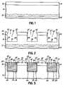
- FIGS. 1-6are diagrammatic cross-sectional views of a portion of a substrate at successive fabrication stages of a processing method in accordance with an embodiment of the invention.
- FIGS. 4A and 5Aare enlarged detailed views of portions of FIGS. 4 and 5 , respectively.
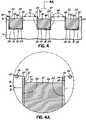
- FIGS. 7 and 8are diagrammatic cross-sectional views of a portion of a substrate at successive fabrication stages subsequent to FIG. 4 of a processing method in accordance with an alternative embodiment of the invention.
- FIG. 9is a diagrammatic cross-sectional view of a portion of a substrate at a fabrication stage subsequent to FIG. 8 of a processing method in accordance with an alternative embodiment of the invention.
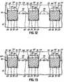
- FIGS. 10-12are diagrammatic cross-sectional views of a portion of a substrate at successive fabrication stages subsequent to FIG. 3 of a processing method in accordance with an alternative embodiment of the invention.
- FIG. 13is a diagrammatic cross-sectional view of a portion of a substrate at a fabrication stage subsequent to FIG. 11 of a processing method in accordance with an alternative embodiment of the invention.
- an insulating layer 10is deposited on a top surface 15 of an underlying substrate 12 .
- Substrate 12may include various circuits and/or devices (not shown) formed thereon and/or therein that may be interconnected by conductive features formed in the insulating layer 10 to define an interconnect level of an interconnect structure.
- the conductive featuresmay interconnect devices of an integrated circuit, and may provide circuit-to-circuit connections, or may establish contact with input and output terminals.
- Substrate 12may also comprise an underlying interconnect level of a multi-level interconnect structure that includes only other conductive features embedded in an insulating layer of dielectric material.
- the insulating layer 10comprises a dielectric material deposited by a conventional method, such as a spin-on application, understood by a person having ordinary skill in the art.
- the dielectric material constituting insulating layer 10may be characterized by a relative permittivity or dielectric constant smaller than the dielectric constant of silicon dioxide, which is about 3.9.
- the dielectric materialmay be characterized by a dielectric constant of about 3.0 or less. Fabricating the insulating layer 10 from such low-k materials may operate to lower the capacitance of the completed interconnect structure as understood by a person having ordinary skill in the art.
- the thickness of the insulating layer 10may range from about 50 nm to about 1,000 nm.
- Candidate low-k dielectric materials for insulating layer 10include, but are not limited to, porous and nonporous spin-on organic low-k dielectrics, porous and nonporous inorganic low-k dielectrics, such as organosilicate glasses, and combinations of organic and inorganic dielectrics.
- a particularly suitable organic low-k dielectric for use in insulating layer 10may be the spin-on aromatic thermoset polymer SiLK commercially available from Dow Chemical Co. (Midland, Mich.) and having a dielectric constant of about 2.6 if nonporous and about 2.2 if porous.
- a particularly suitable inorganic low-k dielectric for use in insulating layer 10may be hydrogen-enriched silicon oxycarbide (SiCOH) deposited, for example, by a deposition recipe based on, for example, plasma enhanced chemical vapor deposition (PECVD) and having a dielectric constant of about 3.0 or less.
- SiCOHsilicon oxycarbide
- PECVDplasma enhanced chemical vapor deposition
- the composition and properties of SiCOHmay vary depending on the deposition conditions and source gases.
- a sacrificial layer 14is formed on a top surface 16 of the insulating layer 10 .
- the sacrificial layer 14may be composed of a dielectric material including, but not limited to, silicon dioxide (SiO 2 ), silicon nitride (Si 3 N 4 ), silicon carbide (SiC), or combinations thereof.
- the thickness of the sacrificial layer 14may range from about 10 nm to about 80 nm.
- features represented by troughs or trenchesare formed in the insulating layer 10 using a conventional lithography and etch operation.
- a resist layer(not shown) is applied to cover a top surface 24 of sacrificial layer 14 , exposed to impart a latent image pattern characteristic of trenches 18 , 20 , 22 , and developed to transform the latent image pattern into a final image pattern having unmasked areas at the future locations of trenches 18 , 20 , 22 .
- Volumes of the unmasked sacrificial layer 14 and insulating layer 12are removed by an etching process, such as plasma etching or reactive ion etching (RIE), capable of producing substantially vertical sidewalls in the insulating layer 10 and sacrificial layer 14 .
- an etching processsuch as plasma etching or reactive ion etching (RIE)
- RIEreactive ion etching
- Trench 18includes sidewalls 26 , 28 that extend substantially vertically in the insulating layer 10 from the top surface 16 to a bottom surface 30 located at a horizontal level or depth intermediate between the top surface 16 and the top surface 15 of substrate 12 .
- Trenches 20 , 22are characterized by sidewalls similar to sidewalls 26 , 28 and a bottom surface similar to bottom surface 30 . Additional features (not shown), such as vias, may be formed in the insulating layer 10 that extend, for example, from the bottom surface 30 of trench 18 to the top surface 15 of substrate 12 .
- Openings 19 , 21 , 23 in the sacrificial layer 14are registered with the trenches 18 , 20 , 22 .
- Each of the openings 19 , 21 , 23is characterized by sidewalls 33 , 35 that are aligned with the sidewalls 26 , 28 of the respective one of the trenches 18 , 20 , 22 .
- the sidewalls 26 , 28 and bottom surface 30 of trenches 18 , 20 , 22are lined with liner layers 32 , 34 , 36 , respectively.
- Each of the liner layers 32 , 34 , 36includes sidewall portions 52 , 54 that cover sidewalls 33 , 35 of each of the openings 19 , 21 , 23 in the sacrificial layer 14 , respectively.
- Exemplary materials for liner layers 32 , 34 , 36include, but are not limited to, titanium nitride (TiN), tantalum nitride (TaN), titanium (Ti), ruthenium (Ru), a tantalum-ruthenium alloy (TaRu), tungsten (W), tungsten nitride (WN), chromium (Cr), niobium (Nb), and other like materials with properties suitable to operate, at the least, as a diffusion barrier and adhesion promoter.
- TiNtitanium nitride
- TaNtantalum nitride
- Tititanium
- Ruruthenium
- TaRutantalum-ruthenium alloy
- Wtungsten
- WNtungsten nitride
- Crchromium
- Nbniobium
- the material constituting liner layers 32 , 34 , 36may be formed utilizing conventional deposition processes familiar to a person having ordinary skill in the art, including but not limited to physical vapor deposition (PVD), ionized-PVD (iPVD), atomic layer deposition (ALD), plasma-assisted ALD, chemical vapor deposition (CVD), and PECVD.
- PVDphysical vapor deposition
- iPVDionized-PVD
- ALDatomic layer deposition
- CVDchemical vapor deposition
- PECVDPECVD
- Conductive lines 38 , 40 , 42are formed in the open volume inside the trenches 18 , 20 , 22 , respectively.
- Conductive lines 38 , 40 , 42are composed of a conductor such as copper (Cu), aluminum (Al), tungsten (W), silver (Ag), alloys of these metals, and other similar metals. These conductors may be deposited by conventional deposition processes, such as CVD, plasma-enhanced CVD, an electrochemical process such as electroplating or electroless plating, chemical solution deposition, PVD, direct current (DC) sputtering, radio frequency (RF) sputtering, and the like.
- CVDchemical vapor deposition
- DCdirect current
- RFradio frequency
- a thin seed layer(not shown) may be deposited in each of the trenches 18 , 20 , 22 to facilitate the formation of the conductive lines 38 , 40 , 42 .
- a chemical-mechanical polishing (CMP) processis used to remove excess conductor from the field of sacrificial layer 14 and to planarize a top surface 46 of each of the conductive lines 38 , 40 , 42 with the top surface 24 of sacrificial layer 14 . Residual amounts 44 of the conductor may remain in and/or on the sacrificial layer 14 .
- the conductive lines 38 , 40 , 42are recessed relative to the top surface 24 of sacrificial layer 14 .
- the top surface 46 of each of the conductive lines 38 , 40 , 42is recessed below the top surface 24 of sacrificial layer 14 .
- a wet etching processmay be used to recess the conductive lines 38 , 40 , 42 selective to the material of the sacrificial layer 14 and selective to the material(s) of the liner layers 32 , 34 , 36 .
- the etchant for the wet etching processmay include, for example, nitric acid (HNO 3 ), hydrochloric acid (HCl), sulfuric acid (H 2 SO 4 ), hydrofluoric acid (HF), or combinations of these acids.
- a wet etching processmay be used, such as the wet etching process disclosed in commonly-assigned application Ser. No. 10/664,017, which published on Mar. 17, 2005 as Publication No. 2005/0056616. The disclosure of this published application is hereby incorporated by reference herein in its entirety.
- dry etching techniquessuch as plasma etching or RIE utilizing an appropriate etch chemistry and recipe, may also be used to recess the top surface 46 of each of the conductive lines 38 , 40 , 42 below the top surface 24 of sacrificial layer 14 .
- the top surface 46 of each of the conductive lines 38 , 40 , 42is recessed relative to top edges 48 , 50 of respective sidewall portions 52 , 54 of the corresponding one of the liner layers 32 , 34 , 36 .
- the top edges 48 , 50project a height or distance, d 1 , above the top surface 46 .
- the distance, d 1may range from about 0.5 nm to about 50 nm above the top surface 46 of each of the conductive lines 38 , 40 , 42 .
- the sidewall portions 52 , 54 of each of the liner layers 32 , 34 , 36remain bounded by the sacrificial layer 14 .
- the top surface 46 of each of the conductive lines 38 , 40 , 42is effectively recessed toward the bottom surface 30 of the respective one of the trenches 18 , 20 , 22 .
- the sacrificial layer 14is removed by, for example, a dilute wet etch process using a HF solution to expose the top surface 16 of the insulating layer 10 .
- the wet etch processremoves the material constituting the sacrificial layer 14 selective to the dielectric material constituting the insulating layer 12 and selective to the material(s) of the liner layers 32 , 34 , 36 and conductive lines 38 , 40 , 42 .
- the residual amounts 44 of the conductor used to form the conductive lines 38 , 40 , 42may be removed concurrently along with the sacrificial layer 14 .
- top edges 48 , 50 of the sidewall portions 52 , 54 of each of the liner layers 32 , 34 , 36project a distance, d 2 , above the top surface 16 of insulating layer 10 . Consequently, the top edges 48 , 50 of the sidewall portions 52 , 54 of each of the liner layers 32 , 34 , 36 are non-planar relative to the top surface 16 , as well as the top surface 46 of each of the conductive lines 38 , 40 , 42 .
- the top surface 46 of each of the conductive lines 38 , 40 , 42is depicted as being located at a level above the top surface 16 of insulating layer 10 , although the invention is not so limited.
- the sidewall portions 52 , 54 of liner layers 32 , 34 , 36which have the projecting top edges 48 , 50 , extend about the entire perimeter of conductive lines 38 , 40 , 42 , respectively, as understood by a person having ordinary skill in the art.
- a portion of the sacrificial layer 14may remain on the insulating layer 10 if the interconnect level construction can tolerate the presence of this residual material.
- a capping layer 56which may comprise a conformal film of a dielectric material such as silicon nitride (Si 3 N 4 ), silicon carbide (SiC), or SiC(N,H), is formed on the top surface 16 of the insulating layer 10 and on the top surface 46 of the conductive lines 38 , 40 , 42 .
- the thickness of the capping layer 56may range from about 5 nm to about 100 nm.
- the capping layer 56operates to form a seal that reduces the likelihood that conductor from the conductive lines 38 , 40 , 42 can diffuse into the dielectric material constituting insulating layer 10 and, thereby, contaminate the constituent dielectric material.
- the projection of the top edges 48 , 50 of the sidewall portions 52 , 54 of each of the liner layers 32 , 34 , 36 above the top surface 16 of insulating layer 10 and the top surface 46 of the conductive lines 38 , 40 , 42cooperates with the conformal film coverage of the capping layer 56 to eliminate planar interfaces found in conventional damascene interconnect structures that are susceptible to electromigration.
- the capping layer 56 and the projection of the top edges 48 , 50 of the sidewall portions 52 , 54 of each of the liner layers 32 , 34 , 36 above the top surface 16 of insulating layer 10 and above the top surface 46 of the conductive lines 38 , 40 , 42cooperate to increase the electromigration resistance of the conductive lines 38 , 40 , 42 .
- Another insulating layer 66which may be composed of the same dielectric materials as insulating layer 10 , is subsequently deposited that covers insulating layer 10 and that may participate in fabricating an overlying interconnect level.
- the completed interconnect levelmay be reproduced or replicated across the surface of substrate 12 by the fabrication procedure described in FIGS. 1-6 .
- Additional interconnect levels, each similar or identical to the completed interconnect level,may be stacked above the completed interconnect level by following a fabrication process identical or similar to that illustrated in FIGS. 1-6 .
- the conductive lines 38 , 40 , 42are capped with a respective one of capping layers 58 , 60 , 62 , which are composed of an electrically conductive material.
- the electrically conductive material constituting the capping layers 58 , 60 , 62may be deposited by a selective deposition process that deposits the electrically conductive material onto the capping layers 58 , 60 , 62 , but fails to deposit the electrically conductive material on non-conductive material containing areas, such as the top surface 16 of insulating layer 10 .
- the thickness of the capping layers 58 , 60 , 62is specified such that a top surface 64 of each capping layers 58 , 60 , 62 is positioned below the corresponding top edges 48 , 50 of the sidewall portions 52 , 54 of a respective one of the liner layers 32 , 34 , 36 .
- the capping layers 58 , 60 , 62are also bounded spatially in a horizontal direction between the sidewall portions 52 , 54 of the respective one of the liner layers 32 , 34 , 36 .
- the electrically conductive material constituting the capping layers 58 , 60 , 62may comprise a metal, such as a cobalt-containing material containing elemental cobalt (Co) with or without incidental impurities, or cobalt in combination with one or more of the elements tungsten (W), phosphorus (P), boron (B), tin (Sn), molybdenum (Mo), ruthenium (Ru), or another suitable element as an alloy, dopant or non-equilibrium mixture.
- the microstructural morphology of the metal constituting the capping layers 58 , 60 , 62may be amorphous or polycrystalline.
- the capping layers 58 , 60 , 62may be deposited by any well known selective deposition process, such as a wet electroless or electroplating process. Electroless or electroplating deposition selectively forms a thin metal film on surfaces wetted by an aqueous solution by reducing a complex metal ion contained in the aqueous solution. The thin metal film does not form on non-metallic surfaces, such as the top surface 24 of sacrificial layer 14 .
- the sacrificial layer 14is removed, as described above with regard to FIG. 5 , selective to the material(s) of the liner layers 32 , 34 , 36 and capping layers 58 , 60 , 62 .
- Another insulating layer 66 of dielectric materialis subsequently deposited that covers the top surface 16 of the insulating layer 10 and the top surface 64 of each of the capping layers 58 , 60 , 62 .
- the electromigration resistance of the conductive lines 38 , 40 , 42is increased by the cooperation between the capping layers 58 , 60 , 62 and the projection of the top edges 48 , 50 of the sidewall portions 52 , 54 of each of the liner layers 32 , 34 , 36 above the top surface 16 of insulating layer 10 and above the top surface 46 of the conductive lines 38 , 40 , 42 .
- conformal capping layer 56is applied as described above with regard to FIG. 6 .
- the conformal capping layer 56further cooperates with capping layers 58 , 60 , 62 and the projection of the top edges 48 , 50 of the sidewall portions 52 , 54 of each of the liner layers 32 , 34 , 36 above the top surface 16 of insulating layer 10 and the top surface 46 of the conductive lines 38 , 40 , 42 to increase the electromigration resistance of the conductive lines 38 , 40 , 42 .
- the conformal capping layer 56is subsequently covered by the insulating layer 66 of dielectric material.
- capping layers 58 , 60 , 62are formed on the top surface 64 of a respective one of the conductive lines 38 , 40 , 42 , as described above with regard to FIG. 7 .
- the top surface 46 of each of the conductive lines 38 , 40 , 42is not recessed relative to the top surface 24 of sacrificial layer 14 before forming the capping layers 58 , 60 , 62 , the top surface 64 of each of the capping layers 58 , 60 , 62 projects above the height of the top edges 48 , 50 of the sidewall portions 52 , 54 of the respective one of the liner layers 32 , 34 , 36 .
- the sacrificial layer 14is removed using an etching process as described above with regard to FIG. 5 .
- the capping layers 58 , 60 , 62may operate as a etch mask for the conductive lines 38 , 40 , 42 during the etching process.
- the top edges 48 , 50 of the sidewall portions 52 , 54 of each of the liner layers 32 , 34 , 36project above the top surface 16 of insulating layer 10 , but not above the top surface 46 of each of the conductive lines 38 , 40 , 42 .
- the etching processmay recess the residual amounts 44 of the conductor used to form the conductive lines 38 , 40 , 42 by a snowplowing effect.
- An interface 70 with an open or uncovered perimeteris present between each of the conductive lines 38 , 40 , 42 and the corresponding one of the capping layers 58 , 60 , 62 because the top edges 48 , 50 of the sidewall portions 52 , 54 of liner layers 32 , 34 , 36 fail to project above the top surface 46 of each of the conductive lines 38 , 40 , 42 .
- an insulating layer 66is applied to the top surface 16 of insulating layer 10 .
- the insulating layer 66covers the top surface 64 of each of the capping layers 58 , 60 , 62 .
- the insulating layer 66which may be formed from the same types of dielectric material as insulating layer 10 , may participate in forming an overlying interconnect level. Residual amounts 44 of the conductor used to form the conductive lines 38 , 40 , 42 are trapped along the interface 65 between the insulating layers 10 , 66 .
- a conformal capping layer 68is deposited, before the insulating layer 66 is applied, on the top surface 16 of insulating layer 10 and the top surface 64 of each of the capping layers 58 , 60 , 62 .
- the conformal capping layer 68has a construction similar to the conformal capping layer 56 described with regard to FIG. 6 .
- the capping layer 68seals the interface 70 between each of the conductive lines 38 , 40 , 42 and the respective one of the capping layers 58 , 60 , 62 .
- the sacrificial layer 14may be omitted in its entirety.
- the conductive lines 38 , 40 , 42may be polished to approximately the top surface 16 of insulating layer 10 before the capping layers 58 , 60 , 62 are formed on the top surface the conductive lines 38 , 40 , 42 and the top surface 16 of the insulating layer 10 is recessed.
- the embodiments of the inventionprovide interconnect structures with high dielectric breakdown resistance and with excellent potential for future technology extendibility.
- the inventionin its various embodiments provides fabrication methods that are compatible with BEOL process flows without introducing additional masking steps or incrementally added cost.
- references herein to terms such as “vertical”, “horizontal”, etc.are made by way of example, and not by way of limitation, to establish a frame of reference.
- the term “horizontal” as used hereinis defined as a plane parallel to a conventional plane of a semiconductor wafer or substrate, regardless of its actual three-dimensional spatial orientation.
- the term “vertical”refers to a direction perpendicular to the horizontal, as just defined. Terms, such as “on”, “above”, “below”, “side” (as in “sidewall”), “higher”, “lower”, “over”, “beneath” and “under”, are defined with respect to the horizontal plane. It is understood that various other frames of reference may be employed for describing the invention without departing from the spirit and scope of the invention.
- onused in the context of two layers means at least some contact between the layers.
- overmeans two layers that are in close proximity, but possibly with one or more additional intervening layers such that contact is possible but not required. As used herein, neither “on” nor “over” implies any directionality.
Landscapes
- Engineering & Computer Science (AREA)
- Physics & Mathematics (AREA)
- Condensed Matter Physics & Semiconductors (AREA)
- General Physics & Mathematics (AREA)
- Manufacturing & Machinery (AREA)
- Computer Hardware Design (AREA)
- Microelectronics & Electronic Packaging (AREA)
- Power Engineering (AREA)
- Internal Circuitry In Semiconductor Integrated Circuit Devices (AREA)
Abstract
Description
Claims (14)
Priority Applications (3)
| Application Number | Priority Date | Filing Date | Title |
|---|---|---|---|
| US11/562,550US7666781B2 (en) | 2006-11-22 | 2006-11-22 | Interconnect structures with improved electromigration resistance and methods for forming such interconnect structures |
| US11/875,193US7984409B2 (en) | 2006-11-22 | 2007-10-19 | Structures incorporating interconnect structures with improved electromigration resistance |
| CN2007101867818ACN101188223B (en) | 2006-11-22 | 2007-11-16 | Interconnection structure and its forming method |
Applications Claiming Priority (1)
| Application Number | Priority Date | Filing Date | Title |
|---|---|---|---|
| US11/562,550US7666781B2 (en) | 2006-11-22 | 2006-11-22 | Interconnect structures with improved electromigration resistance and methods for forming such interconnect structures |
Related Child Applications (1)
| Application Number | Title | Priority Date | Filing Date |
|---|---|---|---|
| US11/875,193Continuation-In-PartUS7984409B2 (en) | 2006-11-22 | 2007-10-19 | Structures incorporating interconnect structures with improved electromigration resistance |
Publications (2)
| Publication Number | Publication Date |
|---|---|
| US20080116582A1 US20080116582A1 (en) | 2008-05-22 |
| US7666781B2true US7666781B2 (en) | 2010-02-23 |
Family
ID=39416129
Family Applications (2)
| Application Number | Title | Priority Date | Filing Date |
|---|---|---|---|
| US11/562,550Active2027-04-29US7666781B2 (en) | 2006-11-22 | 2006-11-22 | Interconnect structures with improved electromigration resistance and methods for forming such interconnect structures |
| US11/875,193Active2027-07-11US7984409B2 (en) | 2006-11-22 | 2007-10-19 | Structures incorporating interconnect structures with improved electromigration resistance |
Family Applications After (1)
| Application Number | Title | Priority Date | Filing Date |
|---|---|---|---|
| US11/875,193Active2027-07-11US7984409B2 (en) | 2006-11-22 | 2007-10-19 | Structures incorporating interconnect structures with improved electromigration resistance |
Country Status (2)
| Country | Link |
|---|---|
| US (2) | US7666781B2 (en) |
| CN (1) | CN101188223B (en) |
Cited By (5)
| Publication number | Priority date | Publication date | Assignee | Title |
|---|---|---|---|---|
| US8802558B2 (en)* | 2012-11-07 | 2014-08-12 | International Business Machines Corporation | Copper interconnect structures and methods of making same |
| US20190189508A1 (en)* | 2017-12-18 | 2019-06-20 | International Business Machines Corporation | Metallic interconnect structures with wrap around capping layers |
| US10431464B2 (en) | 2016-10-17 | 2019-10-01 | International Business Machines Corporation | Liner planarization-free process flow for fabricating metallic interconnect structures |
| US10804193B2 (en) | 2016-04-12 | 2020-10-13 | Tessera, Inc. | Semiconductor interconnect structure with double conductors |
| US11515255B2 (en)* | 2013-03-13 | 2022-11-29 | Taiwan Semiconductor Manufacturing Company, Ltd. | Electro-migration barrier for interconnect |
Families Citing this family (13)
| Publication number | Priority date | Publication date | Assignee | Title |
|---|---|---|---|---|
| US7531384B2 (en)* | 2006-10-11 | 2009-05-12 | International Business Machines Corporation | Enhanced interconnect structure |
| US8138604B2 (en)* | 2007-06-21 | 2012-03-20 | International Business Machines Corporation | Metal cap with ultra-low k dielectric material for circuit interconnect applications |
| KR101532634B1 (en)* | 2008-12-31 | 2015-07-01 | 삼성전자주식회사 | Method and system for detecting defective metal lines in a full-chip |
| US8232200B1 (en)* | 2011-03-18 | 2012-07-31 | International Business Machines Corporation | Methods of forming integrated circuit devices having damascene interconnects therein with metal diffusion barrier layers and devices formed thereby |
| US8637400B2 (en)* | 2011-06-21 | 2014-01-28 | International Business Machines Corporation | Interconnect structures and methods for back end of the line integration |
| KR20130007378A (en)* | 2011-07-01 | 2013-01-18 | 삼성전자주식회사 | Semiconductor device |
| US9269612B2 (en)* | 2011-11-22 | 2016-02-23 | Taiwan Semiconductor Manufacturing Company, Ltd. | Mechanisms of forming damascene interconnect structures |
| US9224640B2 (en)* | 2012-08-17 | 2015-12-29 | Globalfoundries Inc. | Method to improve fine Cu line reliability in an integrated circuit device |
| US8659173B1 (en)* | 2013-01-04 | 2014-02-25 | International Business Machines Corporation | Isolated wire structures with reduced stress, methods of manufacturing and design structures |
| US8962479B2 (en)* | 2013-05-10 | 2015-02-24 | International Business Machines Corporation | Interconnect structures containing nitrided metallic residues |
| US9349636B2 (en) | 2013-09-26 | 2016-05-24 | Intel Corporation | Interconnect wires including relatively low resistivity cores |
| TWI758398B (en)* | 2017-01-24 | 2022-03-21 | 美商應用材料股份有限公司 | Method of forming cobalt layer on substrate |
| US10886168B2 (en)* | 2019-06-04 | 2021-01-05 | International Business Machines Corporation | Surface modified dielectric refill structure |
Citations (22)
| Publication number | Priority date | Publication date | Assignee | Title |
|---|---|---|---|---|
| US5098860A (en) | 1990-05-07 | 1992-03-24 | The Boeing Company | Method of fabricating high-density interconnect structures having tantalum/tantalum oxide layers |
| US5897370A (en) | 1994-08-05 | 1999-04-27 | International Business Machines Corporation | High aspect ratio low resistivity lines/vias by surface diffusion |
| US5930669A (en) | 1997-04-03 | 1999-07-27 | International Business Machines Corporation | Continuous highly conductive metal wiring structures and method for fabricating the same |
| US5933753A (en) | 1996-12-16 | 1999-08-03 | International Business Machines Corporation | Open-bottomed via liner structure and method for fabricating same |
| US6383920B1 (en) | 2001-01-10 | 2002-05-07 | International Business Machines Corporation | Process of enclosing via for improved reliability in dual damascene interconnects |
| US20020098681A1 (en) | 1999-07-27 | 2002-07-25 | Chao-Kun Hu | Reduced electromigration and stressed induced migration of Cu wires by surface coating |
| US20020171147A1 (en) | 2001-05-15 | 2002-11-21 | Tri-Rung Yew | Structure of a dual damascene via |
| US20030116439A1 (en) | 2001-12-21 | 2003-06-26 | International Business Machines Corporation | Method for forming encapsulated metal interconnect structures in semiconductor integrated circuit devices |
| US20030125925A1 (en) | 2001-12-27 | 2003-07-03 | Walther John Stephen | Batch editor for netlists described in a hardware description language |
| US6713835B1 (en) | 2003-05-22 | 2004-03-30 | International Business Machines Corporation | Method for manufacturing a multi-level interconnect structure |
| US20040113235A1 (en) | 2002-12-13 | 2004-06-17 | International Business Machines Corporation | Damascene integration scheme for developing metal-insulator-metal capacitors |
| US20040115921A1 (en) | 2002-12-11 | 2004-06-17 | International Business Machines Corporation | Method for depositing a metal layer on a semiconductor interconnect structure having a capping layer |
| US20040115928A1 (en) | 2002-12-11 | 2004-06-17 | International Business Machines Corporation | Method for depositing a metal layer on a semiconductor interconnect structure |
| US20050032352A1 (en)* | 2003-08-05 | 2005-02-10 | Micron Technology, Inc. | H2 plasma treatment |
| US20050056616A1 (en) | 2003-09-17 | 2005-03-17 | International Business Machines Corporation | Method for isotropic etching of copper |
| US6890828B2 (en) | 2003-06-05 | 2005-05-10 | International Business Machines Corporation | Method for supporting a bond pad in a multilevel interconnect structure and support structure formed thereby |
| US20060202345A1 (en) | 2005-03-14 | 2006-09-14 | Hans-Joachim Barth | Barrier layers for conductive features |
| US20060246718A1 (en) | 2005-04-29 | 2006-11-02 | Kai Frohberg | Technique for forming self-aligned vias in a metallization layer |
| US20070157140A1 (en) | 2005-12-29 | 2007-07-05 | Holesovsky Alan L | Method and computer program product for trimming the analysis of physical layout versus schematic design comparison |
| US20080102599A1 (en)* | 2006-10-31 | 2008-05-01 | International Business Machines Corporation | Reduced leakage interconnect structure |
| US20080116576A1 (en) | 2006-11-21 | 2008-05-22 | Bum Ki Moon | Semiconductor devices and methods of manufacture thereof |
| US20080166870A1 (en) | 2004-06-04 | 2008-07-10 | International Business Machines Corporation | Fabrication of Interconnect Structures |
Family Cites Families (2)
| Publication number | Priority date | Publication date | Assignee | Title |
|---|---|---|---|---|
| US7223654B2 (en)* | 2005-04-15 | 2007-05-29 | International Business Machines Corporation | MIM capacitor and method of fabricating same |
| US7396762B2 (en)* | 2006-08-30 | 2008-07-08 | International Business Machines Corporation | Interconnect structures with linear repair layers and methods for forming such interconnection structures |
- 2006
- 2006-11-22USUS11/562,550patent/US7666781B2/enactiveActive
- 2007
- 2007-10-19USUS11/875,193patent/US7984409B2/enactiveActive
- 2007-11-16CNCN2007101867818Apatent/CN101188223B/enactiveActive
Patent Citations (23)
| Publication number | Priority date | Publication date | Assignee | Title |
|---|---|---|---|---|
| US5098860A (en) | 1990-05-07 | 1992-03-24 | The Boeing Company | Method of fabricating high-density interconnect structures having tantalum/tantalum oxide layers |
| US5897370A (en) | 1994-08-05 | 1999-04-27 | International Business Machines Corporation | High aspect ratio low resistivity lines/vias by surface diffusion |
| US5933753A (en) | 1996-12-16 | 1999-08-03 | International Business Machines Corporation | Open-bottomed via liner structure and method for fabricating same |
| US6429519B1 (en) | 1997-04-03 | 2002-08-06 | International Business Machines Corporation | Wiring structures containing interconnected metal and wiring levels including a continuous, single crystalline or polycrystalline conductive material having one or more twin boundaries |
| US5930669A (en) | 1997-04-03 | 1999-07-27 | International Business Machines Corporation | Continuous highly conductive metal wiring structures and method for fabricating the same |
| US20020098681A1 (en) | 1999-07-27 | 2002-07-25 | Chao-Kun Hu | Reduced electromigration and stressed induced migration of Cu wires by surface coating |
| US6383920B1 (en) | 2001-01-10 | 2002-05-07 | International Business Machines Corporation | Process of enclosing via for improved reliability in dual damascene interconnects |
| US20020171147A1 (en) | 2001-05-15 | 2002-11-21 | Tri-Rung Yew | Structure of a dual damascene via |
| US20030116439A1 (en) | 2001-12-21 | 2003-06-26 | International Business Machines Corporation | Method for forming encapsulated metal interconnect structures in semiconductor integrated circuit devices |
| US20030125925A1 (en) | 2001-12-27 | 2003-07-03 | Walther John Stephen | Batch editor for netlists described in a hardware description language |
| US20040115928A1 (en) | 2002-12-11 | 2004-06-17 | International Business Machines Corporation | Method for depositing a metal layer on a semiconductor interconnect structure |
| US20040115921A1 (en) | 2002-12-11 | 2004-06-17 | International Business Machines Corporation | Method for depositing a metal layer on a semiconductor interconnect structure having a capping layer |
| US20040113235A1 (en) | 2002-12-13 | 2004-06-17 | International Business Machines Corporation | Damascene integration scheme for developing metal-insulator-metal capacitors |
| US6713835B1 (en) | 2003-05-22 | 2004-03-30 | International Business Machines Corporation | Method for manufacturing a multi-level interconnect structure |
| US6890828B2 (en) | 2003-06-05 | 2005-05-10 | International Business Machines Corporation | Method for supporting a bond pad in a multilevel interconnect structure and support structure formed thereby |
| US20050032352A1 (en)* | 2003-08-05 | 2005-02-10 | Micron Technology, Inc. | H2 plasma treatment |
| US20050056616A1 (en) | 2003-09-17 | 2005-03-17 | International Business Machines Corporation | Method for isotropic etching of copper |
| US20080166870A1 (en) | 2004-06-04 | 2008-07-10 | International Business Machines Corporation | Fabrication of Interconnect Structures |
| US20060202345A1 (en) | 2005-03-14 | 2006-09-14 | Hans-Joachim Barth | Barrier layers for conductive features |
| US20060246718A1 (en) | 2005-04-29 | 2006-11-02 | Kai Frohberg | Technique for forming self-aligned vias in a metallization layer |
| US20070157140A1 (en) | 2005-12-29 | 2007-07-05 | Holesovsky Alan L | Method and computer program product for trimming the analysis of physical layout versus schematic design comparison |
| US20080102599A1 (en)* | 2006-10-31 | 2008-05-01 | International Business Machines Corporation | Reduced leakage interconnect structure |
| US20080116576A1 (en) | 2006-11-21 | 2008-05-22 | Bum Ki Moon | Semiconductor devices and methods of manufacture thereof |
Non-Patent Citations (5)
| Title |
|---|
| Gopal Raghavan et al., "Diffusion of copper through dielectric films under bias temperature stress," 1995 Elsevier Science S.A., pp. 168-176. |
| Junji Noguchi et al., "Cu-Ion-Migration Phenomena and its Influence on TDDB Lifetime in Cu Metallization," IEEE 41st Annual International Reliability Physics Symposium, Dallas, Texas, 2003, pp. 287-292. |
| Junji Noguchi et al., "Impact of Low-K Dielectrics and Barrier Metals on TDDB Lifetime on Cu Interconnects," IEEE 39th Annual International Reliability Physics Symposium, Orlando, Florida, 2001, pp. 355-359. |
| Memula, Suresh, (Examiner) U.S. Patent and Trademark Office, Office Action dated as mailed on Apr. 6, 2009 for related U.S. Appl. No. 11/875,193. |
| Wolf et al, Silicon Processing for the VLSI Era, vol. 1: Process Technology, Second Edition, Copyright 2000 by Lattice Press, Sunset Beach, CA, pp. 104 and 375. |
Cited By (12)
| Publication number | Priority date | Publication date | Assignee | Title |
|---|---|---|---|---|
| US8802558B2 (en)* | 2012-11-07 | 2014-08-12 | International Business Machines Corporation | Copper interconnect structures and methods of making same |
| US9159653B2 (en) | 2012-11-07 | 2015-10-13 | Globalfoundries Inc. | Copper interconnect structures and methods of making same |
| US11515255B2 (en)* | 2013-03-13 | 2022-11-29 | Taiwan Semiconductor Manufacturing Company, Ltd. | Electro-migration barrier for interconnect |
| US11923304B2 (en) | 2013-03-13 | 2024-03-05 | Taiwan Semiconductor Manufacturing Company, Ltd. | Electro-migration barrier for interconnect |
| US10804193B2 (en) | 2016-04-12 | 2020-10-13 | Tessera, Inc. | Semiconductor interconnect structure with double conductors |
| US12087685B2 (en) | 2016-04-12 | 2024-09-10 | Tessera Llc | Semiconductor interconnect structure with double conductors |
| US10431464B2 (en) | 2016-10-17 | 2019-10-01 | International Business Machines Corporation | Liner planarization-free process flow for fabricating metallic interconnect structures |
| US10741397B2 (en) | 2016-10-17 | 2020-08-11 | International Business Machines Corporation | Liner planarization-free process flow for fabricating metallic interconnect structures |
| US20190189508A1 (en)* | 2017-12-18 | 2019-06-20 | International Business Machines Corporation | Metallic interconnect structures with wrap around capping layers |
| US10672653B2 (en)* | 2017-12-18 | 2020-06-02 | International Business Machines Corporation | Metallic interconnect structures with wrap around capping layers |
| US11315830B2 (en)* | 2017-12-18 | 2022-04-26 | International Business Machines Corporation | Metallic interconnect structures with wrap around capping layers |
| US11404311B2 (en) | 2017-12-18 | 2022-08-02 | International Business Machines Corporation | Metallic interconnect structures with wrap around capping layers |
Also Published As
| Publication number | Publication date |
|---|---|
| CN101188223B (en) | 2010-12-15 |
| US20080116582A1 (en) | 2008-05-22 |
| US7984409B2 (en) | 2011-07-19 |
| CN101188223A (en) | 2008-05-28 |
| US20080120580A1 (en) | 2008-05-22 |
Similar Documents
| Publication | Publication Date | Title |
|---|---|---|
| US7666781B2 (en) | Interconnect structures with improved electromigration resistance and methods for forming such interconnect structures | |
| US11682624B2 (en) | Method of forming an interconnect structure having an air gap and structure thereof | |
| US7396762B2 (en) | Interconnect structures with linear repair layers and methods for forming such interconnection structures | |
| US11031337B2 (en) | Forming dual metallization interconnect structures in single metallization level | |
| JP5255292B2 (en) | Interconnect structure having two-layer metal cap and method of manufacturing the same | |
| JP5089575B2 (en) | Interconnect structure and method of manufacturing the same | |
| US7550822B2 (en) | Dual-damascene metal wiring patterns for integrated circuit devices | |
| US9059257B2 (en) | Self-aligned vias formed using sacrificial metal caps | |
| KR101650281B1 (en) | Electrically conductive laminate structures, electrical interconnects, and methods of forming electrical interconnects | |
| KR101857915B1 (en) | Interconnect structure and method for forming interconnect structure | |
| US7193327B2 (en) | Barrier structure for semiconductor devices | |
| JPH10189733A (en) | Metal coating method for porous dielectric | |
| US20050146040A1 (en) | Metal spacer in single and dual damascene processing | |
| US10396032B2 (en) | Semiconductor structures | |
| US20180012791A1 (en) | Interconnects with inner sacrificial spacers | |
| KR100590203B1 (en) | Metal pattern formation method of a semiconductor device | |
| US12266607B2 (en) | Bottom barrier free interconnects without voids | |
| US6841471B2 (en) | Fabrication method of semiconductor device |
Legal Events
| Date | Code | Title | Description |
|---|---|---|---|
| AS | Assignment | Owner name:INTERNATIONAL BUSINESS MACHINES CORPORATION, NEW Y Free format text:ASSIGNMENT OF ASSIGNORS INTEREST;ASSIGNORS:HSU, LOUIS LU-CHEN;MANDELMAN, JACK ALLAN;TONTI, WILLIAM ROBERT;AND OTHERS;REEL/FRAME:018546/0720;SIGNING DATES FROM 20061018 TO 20061111 Owner name:INTERNATIONAL BUSINESS MACHINES CORPORATION,NEW YO Free format text:ASSIGNMENT OF ASSIGNORS INTEREST;ASSIGNORS:HSU, LOUIS LU-CHEN;MANDELMAN, JACK ALLAN;TONTI, WILLIAM ROBERT;AND OTHERS;SIGNING DATES FROM 20061018 TO 20061111;REEL/FRAME:018546/0720 | |
| FEPP | Fee payment procedure | Free format text:PAYOR NUMBER ASSIGNED (ORIGINAL EVENT CODE: ASPN); ENTITY STATUS OF PATENT OWNER: LARGE ENTITY | |
| STCF | Information on status: patent grant | Free format text:PATENTED CASE | |
| REMI | Maintenance fee reminder mailed | ||
| FPAY | Fee payment | Year of fee payment:4 | |
| SULP | Surcharge for late payment | ||
| AS | Assignment | Owner name:GLOBALFOUNDRIES U.S. 2 LLC, NEW YORK Free format text:ASSIGNMENT OF ASSIGNORS INTEREST;ASSIGNOR:INTERNATIONAL BUSINESS MACHINES CORPORATION;REEL/FRAME:036550/0001 Effective date:20150629 | |
| AS | Assignment | Owner name:GLOBALFOUNDRIES INC., CAYMAN ISLANDS Free format text:ASSIGNMENT OF ASSIGNORS INTEREST;ASSIGNORS:GLOBALFOUNDRIES U.S. 2 LLC;GLOBALFOUNDRIES U.S. INC.;REEL/FRAME:036779/0001 Effective date:20150910 | |
| FPAY | Fee payment | Year of fee payment:8 | |
| AS | Assignment | Owner name:WILMINGTON TRUST, NATIONAL ASSOCIATION, DELAWARE Free format text:SECURITY AGREEMENT;ASSIGNOR:GLOBALFOUNDRIES INC.;REEL/FRAME:049490/0001 Effective date:20181127 | |
| AS | Assignment | Owner name:GLOBALFOUNDRIES U.S. INC., CALIFORNIA Free format text:ASSIGNMENT OF ASSIGNORS INTEREST;ASSIGNOR:GLOBALFOUNDRIES INC.;REEL/FRAME:054633/0001 Effective date:20201022 | |
| AS | Assignment | Owner name:GLOBALFOUNDRIES INC., CAYMAN ISLANDS Free format text:RELEASE BY SECURED PARTY;ASSIGNOR:WILMINGTON TRUST, NATIONAL ASSOCIATION;REEL/FRAME:054636/0001 Effective date:20201117 | |
| AS | Assignment | Owner name:GLOBALFOUNDRIES U.S. INC., NEW YORK Free format text:RELEASE BY SECURED PARTY;ASSIGNOR:WILMINGTON TRUST, NATIONAL ASSOCIATION;REEL/FRAME:056987/0001 Effective date:20201117 | |
| MAFP | Maintenance fee payment | Free format text:PAYMENT OF MAINTENANCE FEE, 12TH YEAR, LARGE ENTITY (ORIGINAL EVENT CODE: M1553); ENTITY STATUS OF PATENT OWNER: LARGE ENTITY Year of fee payment:12 |