US7664987B2 - Flash memory device with fast reading rate - Google Patents
Flash memory device with fast reading rateDownload PDFInfo
- Publication number
- US7664987B2 US7664987B2US10/851,745US85174504AUS7664987B2US 7664987 B2US7664987 B2US 7664987B2US 85174504 AUS85174504 AUS 85174504AUS 7664987 B2US7664987 B2US 7664987B2
- Authority
- US
- United States
- Prior art keywords
- data
- errors
- memory
- sending
- buffer
- Prior art date
- Legal status (The legal status is an assumption and is not a legal conclusion. Google has not performed a legal analysis and makes no representation as to the accuracy of the status listed.)
- Active, expires
Links
Images


Classifications
- G—PHYSICS
- G06—COMPUTING OR CALCULATING; COUNTING
- G06F—ELECTRIC DIGITAL DATA PROCESSING
- G06F11/00—Error detection; Error correction; Monitoring
- G06F11/07—Responding to the occurrence of a fault, e.g. fault tolerance
- G06F11/08—Error detection or correction by redundancy in data representation, e.g. by using checking codes
- G06F11/10—Adding special bits or symbols to the coded information, e.g. parity check, casting out 9's or 11's
- G06F11/1008—Adding special bits or symbols to the coded information, e.g. parity check, casting out 9's or 11's in individual solid state devices
- G06F11/1068—Adding special bits or symbols to the coded information, e.g. parity check, casting out 9's or 11's in individual solid state devices in sector programmable memories, e.g. flash disk
Definitions
- the present inventionrelates to flash memory, and in particular to flash storage devices that include a flash controller.
- Flash memoryhas become a popular non-volatile memory for a variety of applications, because it offers a superior cost-performance ratio.
- the well-known drawback of flash memoryis its error rate, which is customarily overcome by adding a flash controller that is programmed to manage error correction.
- error correction code6 bytes of such extra data, called ‘error correction code’ (ECC)
- ECCerror correction code
- An object of the present inventionis to provide systems and functionalities for providing error detection and correction to data read from a flash storage device while minimizing the delay caused by the associated processing.
- the present inventionis based on concurrently buffering and checking data sectors read from the flash memory, until the buffer is filled-up. If one or more bad sectors are encountered during the process, these sectors are corrected, the corrected data is written back onto the flash memory, and the current buffer is flagged as a bad buffer.
- the bufferhas been flagged bad, the same data are reread, but now with a high probability to be found valid because they have passed a complete error correction cycle at the flash source.
- the buffer contentif the buffer content has been found valid, the buffer content are transferred to the target device, and the next group of data sectors then are read, copied to the buffer and checked by the flash controller.
- a method of sending data from a memory to a hostincluding the step of: (a) substantially simultaneously: (i) sending the data from the memory to an interface with the host; and (ii) checking the data for errors.
- a method of sending data from a memory to a hostincluding the steps of: (a) for each segment: substantially simultaneously: (i) sending the data from the each segment to a buffer; and (ii) checking the data from the each segment for errors.
- a data storage deviceincluding: (a) a memory for storing the data; (b) at least part of an interface to a host: and (c) a controller operative to substantially simultaneously: (i) send the data from the memory to the interface, and (ii) check the data for errors.
- a method of sending data from a memory to a hostincluding the steps of: (a) sending the data from the memory to a buffer; (b) checking the data for errors; and (c) if a number of the errors that is found by the checking is at least as great as a predetermined threshold: (i) correcting the data, thereby providing corrected data, and (ii) replacing the data in the buffer with the corrected data.
- a method of sending data from a memory to a hostincluding the steps of: (a) for each segment: (i) sending the data from each segment to a buffer, (ii) checking the data from the each segment for errors, and (iii) if a number of the errors that is found by the checking is at least as great as a predetermined threshold: setting an error flag.
- a data storage deviceincluding: (a) a memory for storing the data; (b) at least part of an interface to a host; and (c) a controller operative: (i) to send the data from the memory to a buffer in the interface, (ii) to check the data for errors, and (iii) if a number of the errors that is found by the checking is at least as great as a predetermined threshold: (A) to correct the data, thereby providing corrected data, and (B) to replace the data in the buffer with the corrected data.
- the present inventionis directed towards methods for fast sending, to a host, of data stored in a memory, and towards a data storage device that employs the methods.
- the present inventionis directed primarily towards the reading of data from a flash memory, the scope of the present invention extends to the reading of data from any memory to which the principles of the present invention are applicable.
- the dataare sent, preferably directly, from the memory to an interface with the host, while, substantially simultaneously, the data are checked for errors.
- the dataare corrected, thereby providing corrected data, and the corrected data are written to the memory.
- the corrected dataalso are sent to the interface, preferably directly to the interface. If the number of errors that are found in the course of the checking is less than the predetermined threshold, then the data are sent from the interface to the host.
- the basic method of the present inventionconsists of, for each segment, sending the data stored in that segment, preferably directly, to a buffer, while, substantially simultaneously, checking the data stored in that segment for errors.
- the data stored in that segmentare corrected, thereby providing corrected data; the corrected data are written to that segment; and an error flag is set.
- the dataare sent directly from the segments to the buffer until either all the data have been sent to the buffer or the buffer is full. Then, if the error flag is set, the data are re-sent from the segments to the buffer, preferably directly to the buffer, and the error flag is cleared. If the error flag is not set, the data are sent from the buffer to the host.
- a data storage device of the present inventionincludes a memory for storing the data, at least part of an interface to a host, and a controller for sending the data from the memory to the interface while substantially simultaneously checking the data for errors.
- the dataare sent, preferably directly, to a buffer, and also are checked for errors. If the number of errors that are found in the course of the checking is at least as great as a predetermined threshold, the data are corrected, thereby providing corrected data, and the data in the buffer are replaced with the corrected data. Preferably, if the number of errors is less than the predetermined threshold, the data are sent from the buffer to the host; and if the number of errors is at least as great as the predetermined threshold, the corrected data are written to the memory. More preferably, the replacing of the data in the buffer with the corrected data is effected by sending the corrected data, most preferably directly, from the memory to the buffer.
- the alternative method of the present inventionconsists of, for each segment, sending the data stored in that segment, preferably directly, to a buffer and checking the data for errors. If the number of errors that are found in the course of the checking is at least as great as a predetermined threshold, then an error flag is set. Preferably, for each segment, if the number of errors is at least as great as the predetermined threshold, then the data stored in that segment are corrected, thereby providing corrected data, and the corrected data are written to that segment. Preferably, the sending and the checking continue until either all the data have been sent to the buffer or the buffer is full.
- the error flagis cleared, and the corrected data are sent, most preferably directly, from the segments to the buffer. Only if the error flag is already cleared (i.e., if the error flag has not been set) are the data sent from the buffer to the host.
- An alternative data storage device of the present inventionincludes a memory for storing the data, at least part of an interface to a host, and a controller for sending the data from the memory to a buffer in the interface, for checking the data for errors, and for correcting the data and replacing the data in the buffer with the corrected data if the number of errors found in the data is at least as great as a predetermined threshold.
- FIG. 1is a conceptual illustration of a flash storage device interfaced with a host
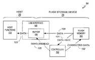
- FIG. 2is a high level conceptual block diagram of a prior art flash storage device interfaced with a host;
- FIG. 3is a flow diagram of reading data from the prior art flash storage device of FIG. 2 ;
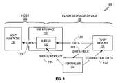
- FIG. 4is a high level conceptual block diagram of a flash storage device of the present invention interfaced with a host;
- FIG. 5is a flow diagram of reading data from the flash storage device of FIG. 4 ;
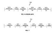
- FIG. 6is a timing diagram for reading data from the prior art flash storage device of FIG. 2 ;
- FIG. 7is a timing diagram for reading data from the flash storage device of FIG. 4 .
- the present inventionis of a method of sending data from a memory to a host, and of a data storage device that employs that method. Specifically, the present invention can be used to read data from a flash memory faster than according to the prior art.
- FIG. 1illustrates the general layout of a data storage and processing system 1 , whether according to the prior art or of the present invention.
- a flash storage device 10incorporating a flash memory and a flash controller, is interfacing with a host device 20 , which is a computerized device such as a personal computer, cellular telephone, digital camera or music player.
- Interface 105such as USB or CompactFlash interface, is resident within both flash storage device 10 and host 20 , to provide the necessary mechanical, electrical and logical interfaces to allow data transfer between the two devices.
- Data transfermay involve read operations, i.e. data sent from flash storage device 10 to host 20 , and/or write operations, i.e. data sent in the opposite direction.
- read operationsi.e. data sent from flash storage device 10 to host 20
- write operationsi.e. data sent in the opposite direction.
- the present inventionfocuses on improving the speed of read operations, and therefore write operations are not described herein. It is presumed, however, that flash storage device 10 already stores data accompanied by ECC (error correction code) that allows error recovery under a selected error-correction algorithm known in the art.
- ECCerror correction code
- Host 20includes host functions 110 , for example all components and software of a personal computer, and the host side of interface 105 , for example a USB interface, for exchanging data with flash storage device 30 .
- Flash storage device 30which is the prior art embodiment of flash storage device 10 of FIG. 1 , includes a flash memory 101 , a controller 100 to control data flow into and from flash memory 101 , and the flash storage device side of interface 105 , for example a USB interface.
- Interface 105includes buffer 106 , preferably a volatile memory, to temporarily store data before transferring the data to host functions 110 .
- Buffer 106is usually implemented within the host part of interface 105 .
- interface 105is a USB interface
- the size of buffer 106is typically 64 kilobytes.
- the focus of the present inventionis on read operations, i.e. transfer of data from flash memory 101 to host functions 110 ; write functions in the opposite directions are therefore not shown, although such write functions will usually exist.
- Data in flash memory 101is stored along with the matching error correction codes (ECC).
- ECCerror correction codes
- data in flash memory 101is organized in sectors of 512 bytes, with added 6 bytes per sector for ECC. Data flow starts by flash memory 101 sending a sector of 512 bytes of data with the associated ECC 121 , to controller 100 .
- Controller 100then compares the ECC to the data content; if an error is found, it is corrected by the error correction algorithm programmed into controller 100 , and the corrected data 122 are written back onto flash memory 101 to fix the error. Controller 100 then sends the original data sector (if found correct) or corrected data sector 124 to buffer 106 , where the data are accumulated until reaching the buffer size, typically 64 kilobytes, or until the end of data flow 121 from flash memory 101 is detected. Then data 123 representative of buffer 106 content are sent to host functions 110 . Data continues to flow this way until completion of the desired data transfer from flash memory 101 to host functions 110 .
- FIG. 3is a flowchart that describes in more detail the data flow process, which usually runs under the initiative and control of host functions 110 in cooperation with controller 100 .
- step 201reading is commenced.
- step 202a data sector of 512 bytes is read from flash memory 101 , and is sent with the associated ECC 121 to controller 100 .
- step 203controller 100 checks the content of the data and ECC to determine whether the data need correction. If in step 204 the data is found to contain errors, then in step 205 the data are corrected using the ECC and the error correction algorithm programmed in controller 100 , and in step 206 the corrected data are written back to flash memory 101 , and then fed to buffer 106 in step 207 .
- step 208buffer 106 is examined whether buffer 106 is full, i.e. whether the accumulated sectors added to buffer 106 by the previous steps have reached its 64-kilobyte capacity. If the answer is negative, the procedure loops back to step 202 for reading another data sector; otherwise, in step 209 the buffer content 123 is sent to host functions 110 , and buffer 106 is cleared. The process loops through step 210 back to step 202 until reaching the last buffer's worth of data, i.e. completing the transfer of the predefined content from flash memory 101 to host functions 110 , and then the process is terminated in step 211 .
- each and every data sector of 512 bytesis checked in step 203 to determine the validity of the data sector with respect to the associated ECC, prior to the data sector being fed into buffer 106 .
- the great majority of sectorsis valid, still checking all sectors slows down the data flow hence the reading process, which is the motive for the present invention.
- FIG. 4 and FIG. 5describe a preferred embodiment 50 of the present invention.
- Flash storage device 70is a preferred embodiment of device 10 of FIG. 1 , constructed in accordance with the present invention. Flash storage device 70 allows direct data transfer 120 from flash memory 101 to buffer 106 , concurrently with sending that data with the associated ECC 121 , to be checked by controller 102 , as opposed to checking and correcting the data before sending the data to buffer 106 . Direct data transfer 120 is managed by control pulses sent by controller 102 to both flash memory 101 and the flash storage device side of USB interface 105 , under methods known to those skilled in the art. A data sector found invalid by controller 102 is corrected and the corrected data 122 are written back onto flash memory 101 as in the prior art described with respect to FIG. 2 . In addition, an error flag is set. However the data 120 transferred to the buffer 106 are the data with the error. Buffer 106 continues to receive data even after an error has been detected, until buffer 106 becomes full.
- controller 102checks whether an error occurred in one of the sectors contained in the buffer 106 . If no error occurred, the data in buffer 106 are correct and can be transferred 123 to host function 110 . If an error did occur, the entire 64 kilobyte buffer 106 has to be reread from the flash 101 , because the data in buffer 106 contain error(s) which were corrected by controller 102 within flash memory 101 . To mark whether the data in buffer 106 are valid or should be reread, controller 102 issues a send/reread command 125 at the end of the transfer, according to the state of the error flag. It will be noted that issuing a send/reread control command 125 when buffer 106 is filled-up is common in the art and is part of the USB protocol.
- the reading procedurestarts in step 221 of FIG. 5 , initiated by host functions 110 and executed through cooperation between host functions 110 and flash controller 102 .
- step 222a data sector of 512 bytes is read from flash memory 101 , along with the respective ECC. Then, concurrently, the procedure is split into step 227 and steps 223 - 226 .
- step 227the data sector 120 , excluding the ECC, is added to buffer 106 .
- step 223the data and ECC 121 are checked, and if found correct in step 224 , the procedure is routed to step 228 ; if an error was found in step 224 , the error is corrected in step 225 by controller 102 applying its error correction algorithm, and the corrected data are written back into flash memory 101 ; also, in step 226 the content of buffer 106 is flagged bad, and control moves to step 228 .
- step 228after completing steps 227 and either 224 or 226 , buffer 106 is checked to determine whether the amount of data has reached the capacity of buffer 106 , e.g. 64 kilobytes. Note that step 223 optionally can be performed in parallel to reading the next data segment in step 222 .
- step 229the status of buffer 106 is checked. If buffer 106 has been flagged bad at any of the previous steps 226 , then buffer 106 and the status flag of buffer 106 are cleared in step 230 , the read pointers are reset to the first sector used as the source for the most recent buffer's worth of data, and the procedure moves to step 222 , to start reading again the same content, which is the ‘reread’ option within the send/reread control signal 125 of FIG. 4 . If however in step 229 the buffer content is found OK, i.e.
- Step 231the content 123 of buffer 106 are sent to host functions 110 and buffer 106 is cleared, as represented by the ‘send’ option within the send/reread control signal 125 of FIG. 4 .
- Step 232examines whether the last buffer's worth of data has been reached, i.e. whether the data transfer between flash memory 101 has been completed; if so, the procedure terminates in step 234 , otherwise the next data sector is read in step 222 .
- steps 222 and 223may be implemented as a single read/check step under methods known in the art for error checking by hardware concurrently with the reading process of a data sector. In this case, block 222 is replaced by a combined block 222 + 223 with read/check functions, and from there concurrent flow is split to blocks 227 and 224 .
- timing diagram 700describes the processes that take place during the read cycle.
- step 202 of FIG. 3data are read from the flash (reference numeral 121 ), then the data are checked for errors in step 203 using the error correction code and then the data are written to the buffer (reference numeral 124 ) in step 207 .
- step 207timing diagram 701 describes the timing of the current invention.
- the data transfer stage 222 of FIG. 5transfers data to both buffer 106 and controller 102 . Then the data are checked in stage 224 using the error correction code, and a new read can commence. It is clearly visible how the current invention is superior to prior art:
- the cycle time of reading one sectoris almost 50% shorter in 701 than in 700 , because there is only one data transfer stage per sector.
- the data buses of flash memory 101 and interface 105are almost 100% busy in 701 , because most of the time is spent in the data transfer stage, whereas in 700 the data buses are less than 50% occupied because the bus of interface 105 is active only in the data-to-buffer stage, and the bus of flash memory 101 is active only in the data-from-flash stage.
- step 224the number of errors found in the data is compared to a predetermined threshold. If the number of errors found in the data is greater than or equal to the predetermined threshold then program flow continues to step 225 ; otherwise, program flow continues to step 228 .
- the “usual” case described aboveis the special case of the threshold being set equal to 1.
- Embodiment 70 of a data storage device of the present inventionincludes flash memory 101 , controller 102 and as much of interface 105 as is included in flash storage device 70 .
- buffer 106is in host 20 ; in other implementations of host 20 and flash storage device 70 , buffer 106 is in flash storage device 70 .
- controllermanages the general operation of flash memory 101 , for example as described in U.S. Pat. Nos. 5,404,485, 5,799,168, 5,937,425 and 6,148,354, all four of which are incorporated by reference for all purposes as if fully set forth herein.
- flash storage device 70among the illustrated components is conceptual and is not intended to indicate that the illustrated components preferably are discrete components. Usually, in fact, controller 102 and much of the part of interface 105 that is included in flash storage device 70 all are fabricated in a common integrated circuit.
Landscapes
- Engineering & Computer Science (AREA)
- Theoretical Computer Science (AREA)
- Quality & Reliability (AREA)
- Physics & Mathematics (AREA)
- General Engineering & Computer Science (AREA)
- General Physics & Mathematics (AREA)
- Techniques For Improving Reliability Of Storages (AREA)
Abstract
Description
Claims (23)
Priority Applications (1)
| Application Number | Priority Date | Filing Date | Title |
|---|---|---|---|
| US10/851,745US7664987B2 (en) | 2003-05-25 | 2004-05-24 | Flash memory device with fast reading rate |
Applications Claiming Priority (2)
| Application Number | Priority Date | Filing Date | Title |
|---|---|---|---|
| US47343703P | 2003-05-25 | 2003-05-25 | |
| US10/851,745US7664987B2 (en) | 2003-05-25 | 2004-05-24 | Flash memory device with fast reading rate |
Publications (2)
| Publication Number | Publication Date |
|---|---|
| US20040250177A1 US20040250177A1 (en) | 2004-12-09 |
| US7664987B2true US7664987B2 (en) | 2010-02-16 |
Family
ID=33493348
Family Applications (1)
| Application Number | Title | Priority Date | Filing Date |
|---|---|---|---|
| US10/851,745Active2026-01-16US7664987B2 (en) | 2003-05-25 | 2004-05-24 | Flash memory device with fast reading rate |
Country Status (1)
| Country | Link |
|---|---|
| US (1) | US7664987B2 (en) |
Cited By (4)
| Publication number | Priority date | Publication date | Assignee | Title |
|---|---|---|---|---|
| US20090044085A1 (en)* | 2007-08-06 | 2009-02-12 | Industrial Technology Research Institute | Defect management method for storage medium and system thereof |
| US20090141602A1 (en)* | 2007-11-29 | 2009-06-04 | Industrial Technology Research Institute | Recording medium structure capable of displaying defect rate |
| US20110035646A1 (en)* | 2009-08-06 | 2011-02-10 | Sony Corporation | Nonvolatile random access memory and nonvolatile memory system |
| US20190163367A1 (en)* | 2015-07-24 | 2019-05-30 | Sandisk Technologies Llc | Optimistic read operation |
Families Citing this family (12)
| Publication number | Priority date | Publication date | Assignee | Title |
|---|---|---|---|---|
| TWI248617B (en)* | 2004-08-13 | 2006-02-01 | Prolific Technology Inc | Data storage device |
| JP4908083B2 (en)* | 2006-06-30 | 2012-04-04 | 株式会社東芝 | Memory controller |
| US20080313495A1 (en)* | 2007-06-13 | 2008-12-18 | Gregory Huff | Memory agent |
| US20090106513A1 (en)* | 2007-10-22 | 2009-04-23 | Chuang Cheng | Method for copying data in non-volatile memory system |
| TW200935433A (en)* | 2008-02-15 | 2009-08-16 | Asmedia Technology Inc | Method for reducing data error when flash memory storage device using copy back command |
| US20110004728A1 (en)* | 2009-07-02 | 2011-01-06 | Ocz Technology Group, Inc. | On-device data compression for non-volatile memory-based mass storage devices |
| JP2014052971A (en)* | 2012-09-10 | 2014-03-20 | Toshiba Corp | Semiconductor integrated circuit |
| US11953988B2 (en) | 2019-05-23 | 2024-04-09 | Micron Technology, Inc. | Error correction memory device with fast data access |
| US11121729B1 (en)* | 2020-07-30 | 2021-09-14 | Seagate Technology Llc | Read channel buffer management for higher throughput decoding |
| US11797396B2 (en) | 2020-07-30 | 2023-10-24 | Seagate Technology Llc | Decoding policy management to support multiple decoding schemes in a single buffer space |
| JP2022036654A (en) | 2020-08-24 | 2022-03-08 | キオクシア株式会社 | Memory device and memory system |
| KR20230000168A (en)* | 2021-06-24 | 2023-01-02 | 에스케이하이닉스 주식회사 | Memory, operation method of memory and operation method of memory system |
Citations (25)
| Publication number | Priority date | Publication date | Assignee | Title |
|---|---|---|---|---|
| US4757445A (en)* | 1983-09-12 | 1988-07-12 | Motorola, Inc. | Method and apparatus for validating prefetched instruction |
| US5396504A (en)* | 1991-06-29 | 1995-03-07 | Samsung Electronics Co., Ltd. | Error correction system of digital data |
| US5404485A (en) | 1993-03-08 | 1995-04-04 | M-Systems Flash Disk Pioneers Ltd. | Flash file system |
| US5742623A (en)* | 1995-08-04 | 1998-04-21 | General Instrument Corporation Of Delaware | Error detection and recovery for high rate isochronous data in MPEG-2 data streams |
| US5793774A (en)* | 1994-11-04 | 1998-08-11 | Fujitsu Limited | Flash memory controlling system |
| US5799168A (en) | 1996-01-05 | 1998-08-25 | M-Systems Flash Disk Pioneers Ltd. | Standardized flash controller |
| US5864649A (en)* | 1994-02-15 | 1999-01-26 | Sony Corporation | Apparatus for recording a digital video signal |
| US5937425A (en) | 1997-10-16 | 1999-08-10 | M-Systems Flash Disk Pioneers Ltd. | Flash file system optimized for page-mode flash technologies |
| US5943348A (en)* | 1997-10-14 | 1999-08-24 | Lsi Logic Corporation | Method to check for burst limiting in error correcting systems |
| US6061824A (en)* | 1998-03-05 | 2000-05-09 | Quantum Corporation | Pipelined error correction for minimizing disk re-reading in hard drives |
| WO2000049488A1 (en) | 1999-02-17 | 2000-08-24 | Memory Corporation Plc | Memory system |
| US6148354A (en) | 1999-04-05 | 2000-11-14 | M-Systems Flash Disk Pioneers Ltd. | Architecture for a universal serial bus-based PC flash disk |
| US6154866A (en)* | 1996-09-30 | 2000-11-28 | Sony Corporation | Reproducing apparatus, error correcting unit and error correcting method |
| US20020027731A1 (en)* | 2000-07-19 | 2002-03-07 | Yutaka Arakawa | Data reproducing unit, data reproducing method of the same, and a magnetic recording/reproducing apparatus |
| US20030093744A1 (en)* | 2001-11-14 | 2003-05-15 | Monilithic System Technology, Inc. | Error correcting memory and method of operating same |
| US6574420B1 (en)* | 1996-09-30 | 2003-06-03 | Matsushita Electric Industrial Co., Ltd. | Recording/reproducing method suitable for recording/reproducing AV data on/from disc, recorder and reproducer for the method, information recording disc and information processing system |
| US20030145274A1 (en)* | 2002-01-23 | 2003-07-31 | Samsung Electronics Co., Ltd. | Decoding method and apparatus therefor |
| US6628892B2 (en)* | 1999-05-12 | 2003-09-30 | Kabushiki Kaisha Toshiba | Digital video recording/playback system with entry point processing function |
| US20040156251A1 (en)* | 2003-02-07 | 2004-08-12 | Renesas Technology Corp. | Nonvolatile memory system |
| US20040187065A1 (en)* | 2003-02-25 | 2004-09-23 | Samsung Electronics Co., Ltd. | Apparatus and method generating error flag for error correction |
| US20040243885A1 (en)* | 2003-06-02 | 2004-12-02 | Fujitsu Limited | Methods and apparatus for correcting data and error detection codes on the fly |
| US20050078584A1 (en)* | 2003-10-09 | 2005-04-14 | Cheertek, Inc. | System and method for error correction in optical disk system |
| US7020798B2 (en)* | 2002-06-27 | 2006-03-28 | Microsoft Corporation | Detecting low-level data corruption |
| US7117387B2 (en)* | 2003-04-16 | 2006-10-03 | Hitachi, Ltd. | Method and apparatus for writing data and validating data in a recording medium |
| US7149930B2 (en)* | 2002-06-25 | 2006-12-12 | Hitachi Global Storage Technologies Japan, Ltd. | Recording/reproducing apparatus |
- 2004
- 2004-05-24USUS10/851,745patent/US7664987B2/enactiveActive
Patent Citations (26)
| Publication number | Priority date | Publication date | Assignee | Title |
|---|---|---|---|---|
| US4757445A (en)* | 1983-09-12 | 1988-07-12 | Motorola, Inc. | Method and apparatus for validating prefetched instruction |
| US5396504A (en)* | 1991-06-29 | 1995-03-07 | Samsung Electronics Co., Ltd. | Error correction system of digital data |
| US5404485A (en) | 1993-03-08 | 1995-04-04 | M-Systems Flash Disk Pioneers Ltd. | Flash file system |
| US5864649A (en)* | 1994-02-15 | 1999-01-26 | Sony Corporation | Apparatus for recording a digital video signal |
| US5793774A (en)* | 1994-11-04 | 1998-08-11 | Fujitsu Limited | Flash memory controlling system |
| US5742623A (en)* | 1995-08-04 | 1998-04-21 | General Instrument Corporation Of Delaware | Error detection and recovery for high rate isochronous data in MPEG-2 data streams |
| US5799168A (en) | 1996-01-05 | 1998-08-25 | M-Systems Flash Disk Pioneers Ltd. | Standardized flash controller |
| US6154866A (en)* | 1996-09-30 | 2000-11-28 | Sony Corporation | Reproducing apparatus, error correcting unit and error correcting method |
| US6574420B1 (en)* | 1996-09-30 | 2003-06-03 | Matsushita Electric Industrial Co., Ltd. | Recording/reproducing method suitable for recording/reproducing AV data on/from disc, recorder and reproducer for the method, information recording disc and information processing system |
| US5943348A (en)* | 1997-10-14 | 1999-08-24 | Lsi Logic Corporation | Method to check for burst limiting in error correcting systems |
| US5937425A (en) | 1997-10-16 | 1999-08-10 | M-Systems Flash Disk Pioneers Ltd. | Flash file system optimized for page-mode flash technologies |
| US6061824A (en)* | 1998-03-05 | 2000-05-09 | Quantum Corporation | Pipelined error correction for minimizing disk re-reading in hard drives |
| US6725321B1 (en)* | 1999-02-17 | 2004-04-20 | Lexar Media, Inc. | Memory system |
| WO2000049488A1 (en) | 1999-02-17 | 2000-08-24 | Memory Corporation Plc | Memory system |
| US6148354A (en) | 1999-04-05 | 2000-11-14 | M-Systems Flash Disk Pioneers Ltd. | Architecture for a universal serial bus-based PC flash disk |
| US6628892B2 (en)* | 1999-05-12 | 2003-09-30 | Kabushiki Kaisha Toshiba | Digital video recording/playback system with entry point processing function |
| US20020027731A1 (en)* | 2000-07-19 | 2002-03-07 | Yutaka Arakawa | Data reproducing unit, data reproducing method of the same, and a magnetic recording/reproducing apparatus |
| US20030093744A1 (en)* | 2001-11-14 | 2003-05-15 | Monilithic System Technology, Inc. | Error correcting memory and method of operating same |
| US20030145274A1 (en)* | 2002-01-23 | 2003-07-31 | Samsung Electronics Co., Ltd. | Decoding method and apparatus therefor |
| US7149930B2 (en)* | 2002-06-25 | 2006-12-12 | Hitachi Global Storage Technologies Japan, Ltd. | Recording/reproducing apparatus |
| US7020798B2 (en)* | 2002-06-27 | 2006-03-28 | Microsoft Corporation | Detecting low-level data corruption |
| US20040156251A1 (en)* | 2003-02-07 | 2004-08-12 | Renesas Technology Corp. | Nonvolatile memory system |
| US20040187065A1 (en)* | 2003-02-25 | 2004-09-23 | Samsung Electronics Co., Ltd. | Apparatus and method generating error flag for error correction |
| US7117387B2 (en)* | 2003-04-16 | 2006-10-03 | Hitachi, Ltd. | Method and apparatus for writing data and validating data in a recording medium |
| US20040243885A1 (en)* | 2003-06-02 | 2004-12-02 | Fujitsu Limited | Methods and apparatus for correcting data and error detection codes on the fly |
| US20050078584A1 (en)* | 2003-10-09 | 2005-04-14 | Cheertek, Inc. | System and method for error correction in optical disk system |
Cited By (8)
| Publication number | Priority date | Publication date | Assignee | Title |
|---|---|---|---|---|
| US20090044085A1 (en)* | 2007-08-06 | 2009-02-12 | Industrial Technology Research Institute | Defect management method for storage medium and system thereof |
| US8332696B2 (en)* | 2007-08-06 | 2012-12-11 | Industrial Technology Research Institute | Defect management method for storage medium and system thereof |
| US20090141602A1 (en)* | 2007-11-29 | 2009-06-04 | Industrial Technology Research Institute | Recording medium structure capable of displaying defect rate |
| US7962810B2 (en)* | 2007-11-29 | 2011-06-14 | Industrial Technology Research Institute | Recording medium structure capable of displaying defect rate |
| US20110035646A1 (en)* | 2009-08-06 | 2011-02-10 | Sony Corporation | Nonvolatile random access memory and nonvolatile memory system |
| US8429494B2 (en)* | 2009-08-06 | 2013-04-23 | Sony Corporation | Nonvolatile random access memory and nonvolatile memory system |
| US20190163367A1 (en)* | 2015-07-24 | 2019-05-30 | Sandisk Technologies Llc | Optimistic read operation |
| US10732847B2 (en)* | 2015-07-24 | 2020-08-04 | Sandisk Technologies Llc | Optimistic read operation |
Also Published As
| Publication number | Publication date |
|---|---|
| US20040250177A1 (en) | 2004-12-09 |
Similar Documents
| Publication | Publication Date | Title |
|---|---|---|
| US7664987B2 (en) | Flash memory device with fast reading rate | |
| US8438457B2 (en) | Nonvolatile memory apparatus, memory controller, and memory system | |
| US9130597B2 (en) | Non-volatile memory error correction | |
| US8713381B2 (en) | Systems and methods of using dynamic data for wear leveling in solid-state devices | |
| JP4908083B2 (en) | Memory controller | |
| US20080222491A1 (en) | Flash memory system for improving read performance and read method thereof | |
| CN109933545B (en) | Data storage device and data processing method of memory device | |
| US20090319843A1 (en) | Method and apparatus for error correction | |
| TWI509624B (en) | Flash memory apparatus, memory controller and method for controlling flash memory | |
| CN102203740A (en) | Data processing method, device and system | |
| US6718506B1 (en) | High speed DVD error correction engine | |
| US20080082872A1 (en) | Memory controller, memory system, and data transfer method | |
| US11726709B2 (en) | Memory control method, memory storage device and memory control circuit unit | |
| US10447314B2 (en) | Decoding method, memory storage device and memory control circuit unit | |
| US20060120166A1 (en) | Data processing apparatus and method for flash memory | |
| CN118535374B (en) | RAID stripe data error correction method, device, equipment and readable storage medium | |
| US9430327B2 (en) | Data access method, memory control circuit unit and memory storage apparatus | |
| TWI566096B (en) | Data storage system and related method | |
| US20130091404A1 (en) | Memory controller and storage device | |
| US10922025B2 (en) | Nonvolatile memory bad row management | |
| US10713160B1 (en) | Data writing method, memory control circuit unit and memory storage device | |
| JP2013131095A (en) | Memory controller, memory device and memory control method | |
| US20110022928A1 (en) | Controller with error correction function, storage device with error correction function, and system with error correction function | |
| US11409596B1 (en) | Encoding control method, memory storage device and memory control circuit unit | |
| US20200379676A1 (en) | Data writing method, memory controlling circuit unit and memory storage device |
Legal Events
| Date | Code | Title | Description |
|---|---|---|---|
| AS | Assignment | Owner name:M-SYSTEMS FLASH DISK PIONEERS LTD., ISRAEL Free format text:ASSIGNMENT OF ASSIGNORS INTEREST;ASSIGNORS:BYCHKOV, EYAL;PALEY, SASHA;MEIR, AVRAHAM;REEL/FRAME:015373/0251 Effective date:20040519 Owner name:M-SYSTEMS FLASH DISK PIONEERS LTD.,ISRAEL Free format text:ASSIGNMENT OF ASSIGNORS INTEREST;ASSIGNORS:BYCHKOV, EYAL;PALEY, SASHA;MEIR, AVRAHAM;REEL/FRAME:015373/0251 Effective date:20040519 | |
| AS | Assignment | Owner name:MSYSTEMS LTD, ISRAEL Free format text:CHANGE OF NAME;ASSIGNOR:M-SYSTEMS FLASH DISK PIONEERS LTD.;REEL/FRAME:021811/0857 Effective date:20060504 Owner name:MSYSTEMS LTD,ISRAEL Free format text:CHANGE OF NAME;ASSIGNOR:M-SYSTEMS FLASH DISK PIONEERS LTD.;REEL/FRAME:021811/0857 Effective date:20060504 | |
| AS | Assignment | Owner name:SANDISK IL LTD., ISRAEL Free format text:CHANGE OF NAME;ASSIGNOR:MSYSTEMS LTD;REEL/FRAME:021874/0513 Effective date:20070101 Owner name:SANDISK IL LTD.,ISRAEL Free format text:CHANGE OF NAME;ASSIGNOR:MSYSTEMS LTD;REEL/FRAME:021874/0513 Effective date:20070101 | |
| STCF | Information on status: patent grant | Free format text:PATENTED CASE | |
| FPAY | Fee payment | Year of fee payment:4 | |
| FPAY | Fee payment | Year of fee payment:8 | |
| AS | Assignment | Owner name:WESTERN DIGITAL ISRAEL LTD, ISRAEL Free format text:CHANGE OF NAME;ASSIGNOR:SANDISK IL LTD;REEL/FRAME:053574/0513 Effective date:20191112 | |
| MAFP | Maintenance fee payment | Free format text:PAYMENT OF MAINTENANCE FEE, 12TH YEAR, LARGE ENTITY (ORIGINAL EVENT CODE: M1553); ENTITY STATUS OF PATENT OWNER: LARGE ENTITY Year of fee payment:12 | |
| AS | Assignment | Owner name:SANDISK ISRAEL LTD., ISRAEL Free format text:CHANGE OF NAME;ASSIGNOR:WESTERN DIGITAL ISRAEL LTD.;REEL/FRAME:071587/0836 Effective date:20250409 |