US7663794B2 - Methods and devices for inhibiting tilting of a movable element in a MEMS device - Google Patents
Methods and devices for inhibiting tilting of a movable element in a MEMS deviceDownload PDFInfo
- Publication number
- US7663794B2 US7663794B2US12/014,675US1467508AUS7663794B2US 7663794 B2US7663794 B2US 7663794B2US 1467508 AUS1467508 AUS 1467508AUS 7663794 B2US7663794 B2US 7663794B2
- Authority
- US
- United States
- Prior art keywords
- movable element
- substrate
- distance
- stationary member
- electrically conductive
- Prior art date
- Legal status (The legal status is an assumption and is not a legal conclusion. Google has not performed a legal analysis and makes no representation as to the accuracy of the status listed.)
- Expired - Fee Related
Links
Images


Classifications
- B—PERFORMING OPERATIONS; TRANSPORTING
- B81—MICROSTRUCTURAL TECHNOLOGY
- B81B—MICROSTRUCTURAL DEVICES OR SYSTEMS, e.g. MICROMECHANICAL DEVICES
- B81B3/00—Devices comprising flexible or deformable elements, e.g. comprising elastic tongues or membranes
- B81B3/0035—Constitution or structural means for controlling the movement of the flexible or deformable elements
- B81B3/0051—For defining the movement, i.e. structures that guide or limit the movement of an element
- G—PHYSICS
- G02—OPTICS
- G02B—OPTICAL ELEMENTS, SYSTEMS OR APPARATUS
- G02B26/00—Optical devices or arrangements for the control of light using movable or deformable optical elements
- G02B26/001—Optical devices or arrangements for the control of light using movable or deformable optical elements based on interference in an adjustable optical cavity
- B—PERFORMING OPERATIONS; TRANSPORTING
- B81—MICROSTRUCTURAL TECHNOLOGY
- B81B—MICROSTRUCTURAL DEVICES OR SYSTEMS, e.g. MICROMECHANICAL DEVICES
- B81B2201/00—Specific applications of microelectromechanical systems
- B81B2201/04—Optical MEMS
- B81B2201/047—Optical MEMS not provided for in B81B2201/042 - B81B2201/045
Definitions
- the inventionrelates generally to microelectromechanical systems (MEMS), and more particularly to interferometric modulators and display devices comprising such interferometric modulators.
- MEMSmicroelectromechanical systems
- Microelectromechanical systemsinclude micro mechanical elements, actuators, and electronics. Micromechanical elements may be created using deposition, etching, and or other micromachining processes that etch away parts of substrates and/or deposited material layers or that add layers to form electrical and electromechanical devices.
- One type of MEMS deviceis called an interferometric modulator.
- interferometric modulator or interferometric light modulatorrefers to a device that selectively absorbs and/or reflects light using the principles of optical interference.
- an interferometric modulatormay comprise a pair of conductive plates, one or both of which may be transparent and/or reflective in whole or part and capable of relative motion upon application of an appropriate electrical signal.
- one platemay comprise a stationary layer deposited on a substrate and the other plate may comprise a metallic membrane separated from the stationary layer by an air gap.
- the position of one plate in relation to anothercan change the optical interference of light incident on the interferometric modulator.
- Such deviceshave a wide range of applications, and it would be beneficial in the art to utilize and/or modify the characteristics of these types of devices so that their features can be exploited in improving existing products and creating new products that have not yet been developed.
- One aspect of the inventionis an interferometric modulator comprising a substrate; an optical layer positioned over the substrate, the optical layer being at least partially transmissive to incident light; a mirror positioned over the substrate and movable between a first position spaced from the optical layer by a first distance and a second position spaced from the optical layer by a second distance, the first distance being greater than the second distance and the mirror having a first surface facing away from the substrate and a second surface facing towards the substrate; and at least one stationary member contacting the second surface of the mirror when the mirror is in the first position, wherein the at least one stationary member is configured to inhibit movement of at least a portion of the mirror when the mirror is in the first position.
- the one or more stationary membersare configured to stabilize the mirror in a manner that improves the optical and/or electromechanical performance of the interferometric modulator and display devices incorporating such interferometric modulators.
- the at least one stationary memberinhibits the movement of at least a portion of the mirror in a direction generally perpendicular to the mirror when the mirror is in the first position.
- the at least one stationary membermay also inhibit the movement of the mirror in a rotational manner and/or in a direction generally parallel to the mirror when the mirror is in the first position.
- the at least one stationary memberinhibits the movement of the mirror in a rotational manner when the mirror is in the second position, and/or when the mirror occupies a position between the first and second positions.
- the at least one stationary membermay also inhibit the movement of the mirror in a direction generally parallel to the mirror when the mirror is in the second position, and/or when the mirror occupies a position between the first and second positions.
- the mirroris substantially planar when in the first position, the second position and/or a position between the first and second positions.
- the mirroris not impinged by light incident to the interferometric modulator and/or light reflected by the interferometric modulator.
- the at least one stationary membercontacts at least a portion of the second surface of the mirror when the mirror is in the first position.
- the interferometric modulatorfurther comprises a mechanical layer attached to the mirror that suspends the mirror over the substrate.
- the mechanical layerexerts a force on the mirror that facilitates contact between the second surface of the mirror and the at least one stationary member when the mirror is in a first position.
- the at least one stationary membermay be of any shape and/or configuration that is capable of performing the functions described herein.
- the at least one stationary membercomprises a single segment that is substantially curvilinear.
- the at least one stationary membercan be, for example, generally hook-shaped or cane-shaped.
- the at least one stationary membercomprises a shaft segment that is substantially perpendicular to the mirror, and a head segment connected to the shaft segment.
- the head segmentmay be substantially parallel to the shaft segment, at an acute angle to the shaft segment, or in any other configuration that allows the at least one stationary member to inhibit at least a portion of the mirror from movement in at least one direction.
- the shaft segmentinhibits lateral movement of at least a portion of the mirror in a direction generally parallel to the mirror when the mirror is in the first position and/or a position between the first and second positions.
- the shaft segmentmay also inhibit rotational movement of at least a portion of the mirror when the mirror is in the first position, the second position, and/or a position between the first and second positions.
- the head segmentinhibits movement of at least a portion of the mirror in a direction generally perpendicular to the mirror when the mirror is in the first position.
- the mirrorcontacts the head segment when the mirror is in the first position.
- the head segmentis wider than the width of at least a portion of the shaft segment.
- the head segmentmay comprise any shape and/or configuration so long as the anti-tilt member is able to inhibit at least a portion of the mirror from movement in at least one direction.
- the shafthas a shape that is conical, substantially rectangular, substantially triangular, and/or substantially round.
- the head segmenthas a shape that is substantially rectangular, substantially conical, barbed, substantially spherical, oblong, and/or substantially hook-shaped.
- the at least one stationary member and/or the mirroris modified to facilitate contact between them and/or aid the at least one stationary member in inhibiting the movement of at least a portion of the mirror.
- the at least one stationary memberfurther comprises a convex portion that contacts at least a portion of the mirror when the mirror is in the first position, the second position, and/or a position between the first and second positions.
- the mirrormay also further comprise a recessed portion that contacts the at least one stationary member when the mirror is in the first position, the second position, and/or a position between the first and second positions.
- a surface of the at least one member and/or the mirroris modified, for example by roughening.
- the at least one stationary membermay also further comprise a contact region that contacts the at least one stationary member when the mirror is in the first position, the second position, and/or a position between the first and second positions.
- the contact regionmay comprise a different material than the other portions of the at least one stationary member.
- the inventionrelates to a member for reducing the movement of a mirror in an interferometric modulator.
- the memberinhibits movement of at least a portion of a mirror in an interferometric modulator in a direction substantially parallel to the mirror, in a direction generally perpendicular to the mirror, and/or in a rotational direction.
- the membermay inhibit movement of at least a portion of the mirror when the mirror is in the first position, the second position, and/or a position between the first and second positions.
- the membercomprises a shaft segment that is substantially perpendicular to the mirror and a head segment connected to the shaft segment.
- the memberinhibits movement of at least a portion of a first mirror of a first interferometric modulator and inhibits movement of at least a portion of a second mirror of a second interferometric modulator.
- the inventionrelates to a visual display device comprising a plurality of interferometric modulators of the invention.
- the visual display devicefurther comprises one or more of the following components: a processor that is in electrical communication with the display, the processor being configured to process image data; a memory device in electrical communication with the processor; a first controller configured to send at least one signal to the display; a second controller configured to send at least a portion of the image data to the first controller; an image source module, which may comprise at least one of a receiver, transceiver, and transmitter, the image source module being configured to send image data to the processor; and/or an input device configured to receive input data and to communicate the input data to the processor.
- the inventionrelates to is an interferometric modulator comprising a substrate; an optical layer positioned over the substrate, the optical layer being at least partially transmissive to incident light; a mirror positioned over the substrate and movable between a first position spaced from the optical layer by a first distance and a second position spaced from the optical layer by a second distance, the first distance being greater than the second distance and the mirror having a first surface facing toward the substrate and a second surface facing away from the substrate; and at least one stationary mirror-stabilizing means configured to maintain the mirror in a desired orientation when the mirror is in the first position, said mirror-stabilizing means contacting the second surface of the mirror when the mirror is in the first position.
- the mirror-stabilizing meansis configured to maintain the mirror in a substantially planar orientation when the mirror is in the first position and/or to maintain the mirror substantially parallel to the substrate when the mirror is in the first position. In some aspects, the mirror-stabilizing means is configured to stabilize the mirror in a manner that improves the optical and/or electromechanical performance of the interferometric modulator.
- the inventionrelates to a process for manufacturing an interferometric modulator of the invention.
- FIG. 1is an isometric view depicting a portion of one embodiment of an interferometric modulator display in which a movable reflective layer of a first interferometric modulator is in a relaxed position and a movable reflective layer of a second interferometric modulator is in an actuated position.
- FIG. 2is a system block diagram illustrating one embodiment of an electronic device incorporating a 3 ⁇ 3 interferometric modulator display.
- FIG. 3is a diagram of movable mirror position versus applied voltage for one exemplary embodiment of an interferometric modulator of FIG. 1 .
- FIG. 4is an illustration of a set of row and column voltages that may be used to drive an interferometric modulator display.
- FIGS. 5A and 5Billustrate one exemplary timing diagram for row and column signals that may be used to write a frame of display data to the 3 ⁇ 3 interferometric modulator display of FIG. 2 .
- FIGS. 6A and 6Bare system block diagrams illustrating an embodiment of a visual display device comprising a plurality of interferometric modulators.
- FIG. 7Ais a cross section of the device of FIG. 1 .
- FIG. 7Bis a cross section of an alternative embodiment of an interferometric modulator.
- FIG. 7Cis a cross section of another alternative embodiment of an interferometric modulator.
- FIG. 7Dis a cross section of yet another alternative embodiment of an interferometric modulator.
- FIG. 7Eis a cross section of an additional alternative embodiment of an interferometric modulator.
- FIG. 8Ais a schematic diagram illustrating an embodiment of a back plane support for a separable interferometric modulator.
- FIG. 8Bis a schematic diagram illustrating an alternative embodiment of a back plane of a separable interferometric modulator.
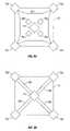
- FIG. 9is a schematic diagram illustrating a layout view of a pixel comprising a 3 ⁇ 3 array of interferometric modulators and anti-tilt members.
- FIGS. 10A-Dare cross-sectional views of several embodiments of anti-tilt members.
- FIG. 11is a cross-sectional view taken along line 11 - 11 of FIG. 9 showing the anti-tilt members located between the adjacent interferometric modulators of the array in FIG. 9 .
- FIG. 12is a diagonal cross-sectional view taken along line 12 - 12 of FIG. 9 showing the post supports for the interferometric modulators of the array in FIG. 9 .
- FIG. 13is a cross-sectional view similar to FIG. 11 that further illustrates the material layers that are applied to manufacture interferometric modulators having the anti-tilt members.
- the embodimentsmay be implemented in or associated with a variety of electronic devices such as, but not limited to, mobile telephones, wireless devices, personal data assistants (PDAs), hand-held or portable computers, GPS receivers/navigators, cameras, MP3 players, camcorders, game consoles, wrist watches, clocks, calculators, television monitors, flat panel displays, computer monitors, auto displays (e.g., odometer display, etc.), cockpit controls and/or displays, display of camera views (e.g., display of a rear view camera in a vehicle), electronic photographs, electronic billboards or signs, projectors, architectural structures, packaging, and aesthetic structures (e.g., display of images on a piece of jewelry).
- MEMS devices of similar structure to those described hereincan also be used in non-display applications such as in electronic switching devices.
- FIG. 1One interferometric modulator display embodiment comprising an interferometric MEMS display element is illustrated in FIG. 1 .
- the pixelsare in either a bright or dark state.
- the display elementIn the bright (“on” or “open”) state, the display element reflects a large portion of incident visible light to a user.
- the dark (“off” or “closed”) stateWhen in the dark (“off” or “closed”) state, the display element reflects little incident visible light to the user.
- the light reflectance properties of the “on” and “off” statesmay be reversed.
- MEMS pixelscan be configured to reflect predominantly at selected colors, allowing for a color display in addition to black and white.
- FIG. 1is an isometric view depicting two adjacent pixels in a series of pixels of a visual display, wherein each pixel comprises a MEMS interferometric modulator.
- an interferometric modulator displaycomprises a row/column array of these interferometric modulators.
- Each interferometric modulatorincludes a pair of reflective layers positioned at a variable and controllable distance from each other to form a resonant optical cavity with at least one variable dimension.
- one of the reflective layersmay be moved between two positions. In the first position, referred to herein as the relaxed position, the movable reflective layer is positioned at a relatively large distance from a fixed partially reflective layer.
- the movable reflective layerIn the second position, referred to herein as the actuated position, the movable reflective layer is positioned more closely adjacent to the partially reflective layer. Incident light that reflects from the two layers interferes constructively or destructively depending on the position of the movable reflective layer, producing either an overall reflective or non-reflective state for each pixel.
- the depicted portion of the pixel array in FIG. 1includes two adjacent interferometric modulators 12 a and 12 b .
- a movable reflective layer 14 ais illustrated in a relaxed position at a predetermined distance from an optical stack 16 a , which includes a partially reflective layer.
- the movable reflective layer 14 bis illustrated in an actuated position adjacent to the optical stack 16 b.
- optical stack 16typically comprise several fused layers, which can include an electrode layer, such as indium tin oxide (ITO), a partially reflective layer, such as chromium, and a transparent dielectric.
- ITOindium tin oxide
- the optical stack 16is thus electrically conductive, partially transparent and partially reflective, and may be fabricated, for example, by depositing one or more of the above layers onto a transparent substrate 20 .
- the layersare patterned into parallel strips, and may form row electrodes in a display device as described further below.
- the movable reflective layers 14 a , 14 bmay be formed as a series of parallel strips of a deposited metal layer or layers (orthogonal to the row electrodes of 16 a , 16 b ) deposited on top of posts 18 and an intervening sacrificial material deposited between the posts 18 . When the sacrificial material is etched away, the movable reflective layers 14 a , 14 b are separated from the optical stacks 16 a , 16 b by a defined gap 19 .
- a highly conductive and reflective materialsuch as aluminum may be used for the reflective layers 14 , and these strips may form column electrodes in a display device.
- the cavity 19remains between the movable reflective layer 14 a and optical stack 16 a , with the movable reflective layer 14 a in a mechanically relaxed state, as illustrated by the pixel 12 a in FIG. 1 .
- a potential differenceis applied to a selected row and column, the capacitor formed at the intersection of the row and column electrodes at the corresponding pixel becomes charged, and electrostatic forces pull the electrodes together.
- the movable reflective layer 14is deformed and is forced against the optical stack 16 .
- a dielectric layerwithin the optical stack 16 may prevent shorting and control the separation distance between layers 14 and 16 , as illustrated by pixel 12 b on the right in FIG. 1 .
- the behavioris the same regardless of the polarity of the applied potential difference. In this way, row/column actuation that can control the reflective vs. non-reflective pixel states is analogous in many ways to that used in conventional LCD and other display technologies.
- FIGS. 2 through 5illustrate one exemplary process and system for using an array of interferometric modulators in a display application.
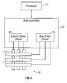
- FIG. 2is a system block diagram illustrating one embodiment of an electronic device that may incorporate aspects of the invention.
- the electronic deviceincludes a processor 21 which may be any general purpose single- or multi-chip microprocessor such as an ARM, Pentium®, Pentium II®, Pentium III®, Pentium IV®, Pentium® Pro, an 8051, a MIPS®, a Power PC®, an ALPHA®, or any special purpose microprocessor such as a digital signal processor, microcontroller, or a programmable gate array.
- the processor 21may be configured to execute one or more software modules.
- the processormay be configured to execute one or more software applications, including a web browser, a telephone application, an email program, or any other software application.
- the processor 21is also configured to communicate with an array driver 22 .
- the array driver 22includes a row driver circuit 24 and a column driver circuit 26 that provide signals to a display array or panel 30 .
- the cross section of the array illustrated in FIG. 1is shown by the lines 1 - 1 in FIG. 2 .
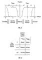
- the row/column actuation protocolmay take advantage of a hysteresis property of these devices illustrated in FIG. 3 . It may require, for example, a 10 volt potential difference to cause a movable layer to deform from the relaxed state to the actuated state. However, when the voltage is reduced from that value, the movable layer maintains its state as the voltage drops back below 10 volts.
- the movable layerdoes not relax completely until the voltage drops below 2 volts.
- There is thus a range of voltage, about 3 to 7 V in the example illustrated in FIG. 3where there exists a window of applied voltage within which the device is stable in either the relaxed or actuated state. This is referred to herein as the “hysteresis window” or “stability window.”
- hysteresis windowor “stability window.”
- the row/column actuation protocolcan be designed such that during row strobing, pixels in the strobed row that are to be actuated are exposed to a voltage difference of about 10 volts, and pixels that are to be relaxed are exposed to a voltage difference of close to zero volts. After the strobe, the pixels are exposed to a steady state voltage difference of about 5 volts such that they remain in whatever state the row strobe put them in. After being written, each pixel sees a potential difference within the “stability window” of 3-7 volts in this example. This feature makes the pixel design illustrated in FIG. 1 stable under the same applied voltage conditions in either an actuated or relaxed pre-existing state.
- each pixel of the interferometric modulatoris essentially a capacitor formed by the fixed and moving reflective layers, this stable state can be held at a voltage within the hysteresis window with almost no power dissipation. Essentially no current flows into the pixel if the applied potential is fixed.
- a display framemay be created by asserting the set of column electrodes in accordance with the desired set of actuated pixels in the first row.
- a row pulseis then applied to the row 1 electrode, actuating the pixels corresponding to the asserted column lines.
- the asserted set of column electrodesis then changed to correspond to the desired set of actuated pixels in the second row.
- a pulseis then applied to the row 2 electrode, actuating the appropriate pixels in row 2 in accordance with the asserted column electrodes.
- the row 1 pixelsare unaffected by the row 2 pulse, and remain in the state they were set to during the row 1 pulse. This may be repeated for the entire series of rows in a sequential fashion to produce the frame.
- the framesare refreshed and/or updated with new display data by continually repeating this process at some desired number of frames per second.
- protocols for driving row and column electrodes of pixel arrays to produce display framesare also well known and may be used in conjunction with the present invention.
- FIGS. 4 and 5illustrate one possible actuation protocol for creating a display frame on the 3 ⁇ 3 array of FIG. 2 .
- FIG. 4illustrates a possible set of column and row voltage levels that may be used for pixels exhibiting the hysteresis curves of FIG. 3 .
- actuating a pixelinvolves setting the appropriate column to ⁇ V bias , and the appropriate row to + ⁇ V, which may correspond to ⁇ 5 volts and +5 volts respectively Relaxing the pixel is accomplished by setting the appropriate column to +V bias , and the appropriate row to the same + ⁇ V, producing a zero volt potential difference across the pixel.
- the pixelsare stable in whatever state they were originally in, regardless of whether the column is at +V bias , or ⁇ V bias .
- voltages of opposite polarity than those described abovecan be used, e.g., actuating a pixel can involve setting the appropriate column to +V bias , and the appropriate row to ⁇ V.
- releasing the pixelis accomplished by setting the appropriate column to ⁇ V bias , and the appropriate row to the same ⁇ V, producing a zero volt potential difference across the pixel.
- FIG. 4it will be appreciated that voltages of opposite polarity than those described above can be used, e.g., actuating a pixel can involve setting the appropriate column to +V bias , and the appropriate row to ⁇ V.
- releasing the pixelis accomplished by setting the appropriate column to ⁇ V bias , and the appropriate row to the same ⁇ V, producing a zero volt potential difference across the pixel.
- actuating a pixelcan involve setting the appropriate column to +V bias , and the appropriate row to ⁇ V.
- releasing the pixelis accomplished by setting the appropriate column to ⁇ V bias , and the appropriate row to the same ⁇ V, producing a zero volt potential difference across the pixel.
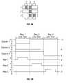
- FIG. 5Bis a timing diagram showing a series of row and column signals applied to the 3 ⁇ 3 array of FIG. 2 which will result in the display arrangement illustrated in FIG. 5A , where actuated pixels are non-reflective.
- the pixelsPrior to writing the frame illustrated in FIG. 5A , the pixels can be in any state, and in this example, all the rows are at 0 volts, and all the columns are at +5 volts. With these applied voltages, all pixels are stable in their existing actuated or relaxed states.
- pixels (1,1), (1,2), (2,2), (3,2) and (3,3)are actuated.
- columns 1 and 2are set to ⁇ 5 volts, and column 3 is set to +5 volts. This does not change the state of any pixels, because all the pixels remain in the 3-7 volt stability window.
- Row 1is then strobed with a pulse that goes from 0, up to 5 volts, and back to zero. This actuates the (1,1) and (1,2) pixels and relaxes the (1,3) pixel. No other pixels in the array are affected.
- column 2is set to ⁇ 5 volts
- columns 1 and 3are set to +5 volts.
- Row 3is similarly set by setting columns 2 and 3 to ⁇ 5 volts, and column 1 to +5 volts.
- the row 3 strobesets the row 3 pixels as shown in FIG. 5A .
- the row potentialsare zero, and the column potentials can remain at either +5 or ⁇ 5 volts, and the display is then stable in the arrangement of FIG. 5A . It will be appreciated that the same procedure can be employed for arrays of dozens or hundreds of rows and columns.
- FIGS. 6A and 6Bare system block diagrams illustrating an embodiment of a display device 40 .
- the display device 40can be, for example, a cellular or mobile telephone.
- the same components of display device 40 or slight variations thereofare also illustrative of various types of display devices such as televisions and portable media players.
- the display device 40includes a housing 41 , a display 30 , an antenna 43 , a speaker 44 , an input device 48 , and a microphone 46 .
- the housing 41is generally formed from any of a variety of manufacturing processes as are well known to those of skill in the art, including injection molding, and vacuum forming.
- the housing 41may be made from any of a variety of materials, including but not limited to plastic, metal, glass, rubber, and ceramic, or a combination thereof.
- the housing 41includes removable portions (not shown) that may be interchanged with other removable portions of different color, or containing different logos, pictures, or symbols.
- the display 30 of exemplary display device 40may be any of a variety of displays, including a bi-stable display, as described herein.
- the display 30includes a flat-panel display, such as plasma, EL, OLED, STN LCD, or TFT LCD as described above, or a non-flat-panel display, such as a CRT or other tube device, as is well known to those of skill in the art.
- the display 30includes an interferometric modulator display, as described herein.
- the components of one embodiment of exemplary display device 40are schematically illustrated in FIG. 6B .
- the illustrated exemplary display device 40includes a housing 41 and can include additional components at least partially enclosed therein.
- the exemplary display device 40includes a network interface 27 that includes an antenna 43 which is coupled to a transceiver 47 .
- the transceiver 47is connected to a processor 21 , which is connected to conditioning hardware 52 .
- the conditioning hardware 52may be configured to condition a signal (e.g. filter a signal).
- the conditioning hardware 52is connected to a speaker 45 and a microphone 46 .
- the processor 21is also connected to an input device 48 and a driver controller 29 .
- the driver controller 29is coupled to a frame buffer 28 , and to an array driver 22 , which in turn is coupled to a display array 30 .
- a power supply 50provides power to all components as required by the particular exemplary display device 40 design.
- the network interface 27includes the antenna 43 and the transceiver 47 so that the exemplary display device 40 can communicate with one or more devices over a network. In one embodiment the network interface 27 may also have some processing capabilities to relieve requirements of the processor 21 .
- the antenna 43is any antenna known to those of skill in the art for transmitting and receiving signals. In one embodiment, the antenna transmits and receives RF signals according to the IEEE 802.11 standard, including IEEE 802.11(a), (b), or (g). In another embodiment, the antenna transmits and receives RF signals according to the BLUETOOTH standard. In the case of a cellular telephone, the antenna is designed to receive CDMA, GSM, AMPS or other known signals that are used to communicate within a wireless cell phone network.
- the transceiver 47pre-processes the signals received from the antenna 43 so that they may be received by and further manipulated by the processor 21 .
- the transceiver 47also processes signals received from the processor 21 so that they may be transmitted from the exemplary display device 40 via the antenna 43 .
- the transceiver 47can be replaced by a receiver.
- network interface 27can be replaced by an image source, which can store or generate image data to be sent to the processor 21 .
- the image sourcecan be a digital video disc (DVD) or a hard-disc drive that contains image data, or a software module that generates image data.
- Processor 21generally controls the overall operation of the exemplary display device 40 .
- the processor 21receives data, such as compressed image data from the network interface 27 or an image source, and processes the data into raw image data or into a format that is readily processed into raw image data.
- the processor 21then sends the processed data to the driver controller 29 or to frame buffer 28 for storage.
- Raw datatypically refers to the information that identifies the image characteristics at each location within an image. For example, such image characteristics can include color, saturation, and gray-scale level.
- the processor 21includes a microcontroller, CPU, or logic unit to control operation of the exemplary display device 40 .
- Conditioning hardware 52generally includes amplifiers and filters for transmitting signals to the speaker 45 , and for receiving signals from the microphone 46 .
- Conditioning hardware 52may be discrete components within the exemplary display device 40 , or may be incorporated within the processor 21 or other components.
- the driver controller 29takes the raw image data generated by the processor 21 either directly from the processor 21 or from the frame buffer 28 and reformats the raw image data appropriately for high speed transmission to the array driver 22 . Specifically, the driver controller 29 reformats the raw image data into a data flow having a raster-like format, such that it has a time order suitable for scanning across the display array 30 . Then the driver controller 29 sends the formatted information to the array driver 22 .
- a driver controller 29such as a LCD controller, is often associated with the system processor 21 as a stand-alone Integrated Circuit (IC), such controllers may be implemented in many ways. They may be embedded in the processor 21 as hardware, embedded in the processor 21 as software, or fully integrated in hardware with the array driver 22 .
- the array driver 22receives the formatted information from the driver controller 29 and reformats the video data into a parallel set of waveforms that are applied many times per second to the hundreds and sometimes thousands of leads coming from the display's x-y matrix of pixels.
- driver controller 29is a conventional display controller or a bi-stable display controller (e.g., an interferometric modulator controller).
- array driver 22is a conventional driver or a bi-stable display driver (e.g., an interferometric modulator display).
- a driver controller 29is integrated with the array driver 22 .
- display array 30is a typical display array or a bi-stable display array (e.g., a display including an array of interferometric modulators).
- the input device 48allows a user to control the operation of the exemplary display device 40 .
- input device 48includes a keypad, such as a QWERTY keyboard or a telephone keypad, a button, a switch, a touch-sensitive screen, a pressure- or heat-sensitive membrane.
- the microphone 46is an input device for the exemplary display device 40 . When the microphone 46 is used to input data to the device, voice commands may be provided by a user for controlling operations of the exemplary display device 40 .
- Power supply 50can include a variety of energy storage devices as are well known in the art.
- power supply 50is a rechargeable battery, such as a nickel-cadmium battery or a lithium ion battery.
- power supply 50is a renewable energy source, a capacitor, or a solar cell, including a plastic solar cell, and solar-cell paint.
- power supply 50is configured to receive power from a wall outlet.
- control programmabilityresides, as described above, in a driver controller which can be located in several places in the electronic display system. In some cases control programmability resides in the array driver 22 . Those of skill in the art will recognize that the above-described optimization may be implemented in any number of hardware and/or software components and in various configurations.
- FIGS. 7A-7Eillustrate five different embodiments of the movable reflective layer 14 and its supporting structures.
- FIG. 7Ais a cross section of the embodiment of FIG. 1 , where a strip of metal material 14 is deposited on orthogonally extending supports 18 .
- FIG. 7Bthe moveable reflective layer 14 is attached to supports at the corners only, on tethers 32 .
- FIG. 7Cthe moveable reflective layer 14 is suspended from a deformable layer 34 , which may comprise a flexible metal.
- the deformable layer 34connects, directly or indirectly, to the substrate 20 around the perimeter of the deformable layer 34 .
- connection postsare herein referred to as support posts.
- the embodiment illustrated in FIG. 7Dhas support post plugs 42 upon which the deformable layer 34 rests.
- the movable reflective layer 14remains suspended over the cavity, as in FIGS. 7A-7C , but the deformable layer 34 does not form the support posts by filling holes between the deformable layer 34 and the optical stack 16 . Rather, the support posts are formed of a planarization material, which is used to form support post plugs 42 .
- the embodiment illustrated in FIG. 7Eis based on the embodiment shown in FIG. 7D , but may also be adapted to work with any of the embodiments illustrated in FIGS. 7A-7C as well as additional embodiments not shown. In the embodiment shown in FIG. 7E , an extra layer of metal or other conductive material has been used to form a bus structure 44 . This allows signal routing along the back of the interferometric modulators, eliminating a number of electrodes that may otherwise have had to be formed on the substrate 20 .
- the interferometric modulatorsfunction as direct-view devices, in which images are viewed from the front side of the transparent substrate 20 , the side opposite to that upon which the modulator is arranged.
- the reflective layer 14optically shields the portions of the interferometric modulator on the side of the reflective layer opposite the substrate 20 , including the deformable layer 34 . This allows the shielded areas to be configured and operated upon without negatively affecting the image quality.
- Such shieldingallows the bus structure 44 in FIG. 7E , which provides the ability to separate the optical properties of the modulator from the electromechanical properties of the modulator, such as addressing and the movements that result from that addressing.
- This separable modulator architectureallows the structural design and materials used for the electromechanical aspects and the optical aspects of the modulator to be selected and to function independently of each other.
- the embodiments shown in FIGS. 7C-7Ehave additional benefits deriving from the decoupling of the optical properties of the reflective layer 14 from its mechanical properties, which are carried out by the deformable layer 34 .
- Thisallows the structural design and materials used for the reflective layer 14 to be optimized with respect to the optical properties, and the structural design and materials used for the deformable layer 34 to be optimized with respect to desired mechanical properties.
- FIGS. 8 a and 8 bdepict views from the back of the modulator, which may also be seen as the bottom of the modulator shown in FIG. 1 .
- the deformable layer 34is in the form of a flexible membrane supported at its corners by support posts 72 a - d , which are anchored in the substrate 20 and/or a layer above the substrate 20 , such as the optical stack 16 .
- the support posts 72 a - dare in the form of support post plugs 42 .
- the deformable layer 34connects to the underlying reflective layer 14 , demarcated by the dotted line, via a large center back support 74 and four smaller surrounding supports 76 a - d .
- the back support 74 and the surrounding supports 76 a - dcan be comprised of the same planarization material as support post plugs 42 , or of any suitable material.
- the deformable layer 34suspends the reflective layer 14 over the optical stack 16 .
- the deformable layer 34is patterned to form thin, linear straps 78 a - d connected to each support post 72 a - d .
- the strapsare attached to the reflective layer 14 by the center support 74 .
- the configurations of FIGS. 8A and 8Bare two alternatives, among many possibilities.
- Interferometric modulators useful in the inventionmay comprise any configuration that gives the desired freedom of movement to the reflective layer 14 and the desired mechanical characteristics of that movement.
- suspension of the reflective layer 14 by a deformable layer 34can present additional challenges.
- the suspended reflective layer 14may be subject to movements and/or deformations that effect the optical properties of the interferometric modulator. Such movements may degrade the quality of a display incorporating interferometric modulators.
- the reflective layer 14may be subject to tilting and/or curling when the reflective layer 14 is in the unconstrained or quiescent position.
- the reflective layer 14may also be subject to undesirable movements in the lateral and/or rotational directions when the reflective layer 14 is in the quiescent position.
- the reflective layer 14abuts the optical stack 16 , or a layer directly or indirectly above the optical stack 16 , in the actuated position. In these embodiments, tilting and/or curling of the reflective layer 14 would generally not occur as frequently as in the quiescent position. However, the reflective layer 14 may still be subject to undesirable movements when in the actuated position, such as lateral and/or rotational movements. Moreover, the reflective layer 14 may be subject to undesirable movements and/or deformations when in a position between the quiescent and actuated positions.
- one or more members 90may be incorporated into the structure of the interferometric modulator to maintain the reflective layer 14 in a position and/or a conformation that allows a desired optical output.
- These one or more membersare herein referred to as “anti-tilt members” 90 .
- the anti-tilt members 90inhibit undesirable movements and/or deformations of the reflective layer 14 by providing stationary abutments or contact points with the reflective layer 14 that stabilize the reflective layer 14 and/or constrain the range of movement of the reflective layer 14 .
- the abutmentscontact the top surface of the reflective layer 14 (i.e.
- the anti-tilt members 90can inhibit the movement of the reflective layer 14 away from the substrate 20 when the reflective layer 14 is in the quiescent position, and/or maintain the reflective layer 14 in an orientation that is substantially parallel to the optical stack 16 when the reflective layer 14 is in the quiescent position. In other embodiments, the anti-tilt members 90 maintain the reflective layer 14 at a fixed angle (i.e. in a non-parallel orientation) relative to the optical stack 16 when the reflective layer 14 is in the quiescent position, so as to produce a desired optical response in the quiescent state.
- contact between the anti-tilt members 90 and the reflective layer 14 when the reflective layer 14 is in the quiescent positionmaintains the reflective layer 14 in a substantially planar orientation, thus inhibiting curling and/or other undesirable deformations of the reflective layer 14 .
- the anti-tilt members 90are designed to maximize the proportion of the surface area of the reflective layer 14 that is in contact with the anti-tilt member(s) 90 when the reflective layer 14 is in the quiescent position, in order to enhance the ability of the anti-tilt member(s) 90 to maintain the reflective layer 14 in a substantially planar orientation when in the quiescent position.
- the number and/or configuration of anti-tilt members 90 utilized in the interferometric modulators of the inventionmay also be designed to aid in maintaining the reflective layer 14 in a substantially planar orientation.
- the anti-tilt members 90may occupy one or more fixed positions that define a range of movement of the reflective layer 14 by contacting the reflective layer 14 if the reflective layer 14 moves outside of a path defined by the one or more anti-tilt members 90 .
- anti-tilt members 90 located along the periphery of the reflective layer 14may inhibit movement of the reflective layer 14 in a direction substantially parallel to the optical stack 16 , and/or in a rotational direction.
- the anti-tilt membersmay generally be comprised of any material and may occupy any position and/or configuration that allows them to perform their desired structural function(s). Several embodiments of the anti-tilt members are described more fully below.
- FIG. 9is a plan view of the back (i.e., the side opposite the substrate 20 ) of a 3 ⁇ 3 array of interferometric modulators, such as those shown in FIGS. 7C-7E , which comprise a pixel 80 in a display.
- each interferometric modulatorincludes four anti-tilt members, for example 90 ( a ), 90 ( b ), 90 ( c ), 90 ( d ), with one anti-tilt member 90 substantially bisecting each side of each interferometric modulator.
- any number and/or placement of the anti-tilt membersmay be used.
- the anti-tilt members 90 located between adjacent interferometric modulatorsare shared by the same interferometric modulators.
- the anti-tilt members located around the periphery of the pixel 80such as anti-tilt members 90 ( a ) and 90 ( d ), are utilized by a single interferometric modulator within pixel 80 .
- the location of the interferometric modulator within the pixel 80need not dictate the arrangement of anti-tilt members 90 .
- additional anti-tilt members 90can be incorporated to suit a specific application.
- the anti-tilt members 90can prevent undesirable movements and/or deformations of the reflective layer 14 , such as movement in a direction substantially perpendicular to the substrate beyond a certain height (gap) with respect to the optical stack 16 .
- each of the interferometric modulators illustrated in FIG. 9is associated with four anti-tilt members 90 , more or less anti-tilt members 90 could be used and still provide the desired benefit of inhibiting undesirable movements of the reflective layer 14 , such as curling and tilting.
- two anti-tilt members 90could be located on two of the four sides (opposing or adjacent sides) of the interferometric modulators (not shown).
- the anti-tilt members 90are located at the corners of the interferometric modulator, for example extending from support posts 42 (for illustrative purposes, optional bus structures 44 are not shown).
- the locations of the anti-tilt members 90 around the periphery of the interferometric modulatorare selected so as not to interfere with the corner posts 42 or deformable mechanical layer 34 .
- the number of anti-tilt members 90can be different for the sub-pixels or sub-components of the pixel 80 based on, for example, the colors of the sub-components, the depths of the cavities, the sub-components' proximity to the outer perimeter of the display, and/or material properties of the sub-components.
- Reflective layers 14 that extend farther across a cavity, for example those reflecting red light, or reflective layers 14 located at the perimeter of a displaymay both be more susceptible to curling and/or tilting than reflective layers 14 associated with shallower optical cavities or located at the interior of the display.
- each pixel 80 in a displaycan include a different number of anti-tilt members 90 . Additional anti-tilt members 90 can be used to secure a relatively large interferometric modulator for greater stability.
- the anti-tilt members 90are shown in FIG. 9 as having a generally rectangular shape. However, the anti-tilt members may comprise a variety of shapes, as described in more detail below. For example, the shape and/or size of the portions of the anti-tilt members 90 that overlap with the reflective layer 14 may be designed so as to enhance the ability of the anti-tilt members 90 to prevent undesirable movements and/or deformations of the reflective layer 14 .
- the anti-tilt members 90are located behind the reflective layer 14 , and thus are essentially invisible to the human eye due to the optical shielding afforded by the reflective layer 14 .
- the anti-tilt memberscan be distributed across the back side of the cavity so as to affect operation of the entire reflective layer 14 without affecting the optical performance of the interferometric modulator or the display device incorporating such interferometric modulators.
- the deformable layer 34is not shown in FIG. 9 . Examples of possible configurations of the deformable layer 34 on the back of an interferometric modulator are shown in FIGS. 8A and 8B , above.
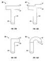
- FIG. 10is a schematic illustration of several embodiments of the anti-tilt members 90 .
- FIGS. 10 a and 10 bare schematic illustrations of a cross-sectional view of anti-tilt members, such as 90 ( b ) and 90 ( c ) in FIG. 9 , each of which function in connection with two adjacent interferometric modulators.
- FIGS. 10 c and 10 dare schematic illustrations of anti-tilt members, such as 90 ( a ) and 90 ( d ) in FIG. 9 , which function with respect to a single interferometric modulator.
- the anti-tilt members 90have a post, shank, shaft, or other structure 94 , referred to herein as a “shaft segment” 94 , which is oriented in a substantially upright position relative to the substrate 20 , as well as a head segment 92 attached to an end of the shaft segment 94 .
- the distal end 98 of the shaft segment 94is attached to the optical stack 16 , or to another stationary layer located directly or indirectly above or below the optical stack 16 , such as the substrate 20 .
- the distal end 98 of the shaft segment 94 or another region of the anti-tilt member 90may also be attached to any other structure that can provide suitable support for the anti-tilt member 90 .
- the head segment 92is attached to the end of the shaft segment 94 opposite the distal end 98 . The structure and function of the head segment is described in more detail below.
- the shaft segment 94may comprise a material that can be the same as the material used for the corner posts 42 , or any other suitable material.
- the shaft segment 94has a height, width and shape sufficient to perform its structural function.
- the width of a particular shaft segment 94may depend upon the material chosen for the shaft segment 94 .
- the shaft segment 94has a width of between about 0.1 micron and 10 microns and particularly about 3 microns.
- the height of the shaft segment 94may depend on the height of the gap between the reflective layer 14 and the optical stack 16 in the interferometric modulator.
- the shaft segmenthas a height of about 1 micron to about 10 microns.
- the shaft segment 94has a slight conical shape.
- the shaft segment 94may be formed in any of a variety of elongated shapes in addition to the slightly conical shape shown in the illustrated embodiments, such as round, rectangular, square, triangular and the like to suit a particular application.
- a round shapemay be preferred to simplify the manufacture of the anti-tilt member 90 , although any shape can be used.
- the anti-tilt members illustrated in FIG. 10comprise a head segment 92 that contacts the reflective layer 14 when the reflective layer is in the quiescent position.
- the head segment 92may comprise one or more elements described below, or any structure capable of performing its structural function(s).
- the head segment 92may comprise is a protrusion that extends from the shaft segment 94 .
- the protrusionmay comprise an enlarged tip or other structure located at the end of the shaft segment 94 that is distal to the optical stack 16 .
- at least a portion of the width of the head segment 92is larger than the width of the shaft segment 94 , having a width of, for example, about 2 to 4 times or more of the width of the shaft segment 94 .
- the shape and size of the head segmentis designed to maximize the surface area of contact between the head segment 92 and a surface of the reflective layer 14 when the reflective layer 14 is in the quiescent position, so as to help maintain the reflective layer 14 in a planar orientation.
- the head segment 92may be oriented substantially perpendicular to the shaft segment 94 , as shown in FIGS. 10 a - 10 c , at an acute angle to the shaft segment 94 (not shown), or in any other orientation with respect to the shaft segment 94 that allows the anti-tilt member to perform its intended functions.
- the head segment 92may extend from the shaft segment 94 any distance that allows the head segment 92 to perform its structural function.
- the head segment 92extends a sufficient distance from the shaft segment 94 such that the anti-tilt member(s) 90 maintains the reflective layer 14 in a planar orientation when the reflective layer 14 is in contact with the anti-tilt member 90 in the quiescent position.
- the head segment 92can take a variety of other shapes, for example, solid or hollow conicals, arrowheads, barbs, spheres, mushroom heads, and other types of projecting structures.
- the shaft segment 94 and head segment 92are in the shape of a cane or a hook, as shown in FIG. 10 d , or other structure having a curved region extending above the top surface of the reflective layer 14 .
- the cane shapemay be advantageous by allowing the support posts 42 and anti-tilt members 90 to be machined during the same processing step.
- a relatively blunt end of the head segment 92is preferred to avoid snagging or interfering with the deformable layer 34 , a backside bus 44 , and/or other structural components of the interferometric modulator.
- the portion(s) of the anti-tilt member 90 that interact with the reflective layer 14are modified to facilitate the stability or other aspect of the interaction.
- the underside 96 of the headmay comprise an abutment which contacts the top surface of the reflective layer 14 to inhibit curling, tilting, and/or other undesirable movements of the reflective layer 14 when the reflective layer 14 is in the quiescent position.
- the underside 96is generally planar. However, the underside 96 may be modified to facilitate contact with the reflective layer 14 , such as being curved in a concave fashion to form a recess in which a portion of the reflective layer 14 may rest (not shown). The underside 96 may also be curved in a convex fashion to form a protrusion that interacts with a recessed portion of the reflective layer 14 (not shown). The underside 96 may also have a surface which is roughened or which incorporates ridges or other snagging devices (not shown) to further assist in stabilizing the reflective layer 14 . However, the underside 96 may also be smooth, for less expensive fabrication costs.
- the head segment 92may also comprise a hook, as shown in FIG. 10 d .
- the hookmay have a radial portion which extends outwardly from the shaft 94 .
- the hookcan have a curved portion distal the shaft 94 and positioned toward a distal end of the radial portion (not shown).
- the curved portioncan be sized and configured to accept a recess or receptacle in the top surface of the reflective layer 14 so as to provide lateral stability of the reflective layer 14 (not shown).
- the recess or receptacleis an additional feature of some embodiments of the reflective layer 14 .
- the curved portionhas a chamfer or taper along the distal circumference to allow the curved portion to easily fit the recess in the top surface of the reflective layer 14 .
- the radial portionmay contact the top surface of the reflective layer 14 .
- the shaft segment 94 and head segment 92can also take the form of a clip (not shown) formed on the surface of the optical stack 16 , or another stationary layer directly or indirectly above or below the optical stack 16 .
- the clipis sized and shaped to fit around the outer portion of the reflective layer 14 while allowing the reflective layer 14 to translate within the cavity.
- the clipcan be configured in a variety of ways to achieve its purpose.
- the clipis substantially C-shaped, with the concave region of the clip forming a portion within which the reflective layer 14 is captured.
- the lower portion of the C-shaped clipis attached to and rests upon the optical stack 16 .
- a pair of semi-rigid, inverted L-shaped membersthat are closely spaced apart and back-to-back inhibit undesirable movements and/or deformation of the reflective layers 14 of two adjacent interferometric modulators.
- a variety of other clip configurationssuch as a single L-shaped clip or a single T-shaped clip, can be used to achieve the purpose of the anti-tilt members.
- FIG. 10 bshows the head segment 92 having a generally rectangular shape with a stepped top surface.
- Each end of the rectangular head segment 92extends towards a different interferometric modulator.
- the stepped top surfacecorresponds to the change in depth of the cavities of adjacent interferometric modulators due to the differences in the distances between the reflective layers 14 and the optical stack 16 when the reflective layers 14 are in the quiescent position.
- the interferometric modulator incorporating the left side of the anti-tilt member 90has a shallower cavity than the cavity for the adjacent interferometric modulator incorporating the right side of the anti-tilt member.
- a flat head, a multi-stepped head, or any suitably shaped headcan also be used.
- the head segment 92may not include a step, as shown in FIG. 10 a .
- the anti-tilt member 90functions in connection with a single interferometric modulator, such as anti-tilt members 90 ( a ) and 90 ( c ) in FIG. 9
- only a single head segment 92is attached to the shaft segment 94 , as shown in FIGS. 10 c and 10 d .
- the thickness(es) of the head segment 92can be varied depending on the material properties of the head segment 92 .
- the anti-tilt members 90extend in an upright direction from the optical stack 16 , or from another stationary layer directly or indirectly above or below the optical stack 16 , such as the substrate.
- the shaft segments 94can have a variety of lengths and a variety of distances between them, depending upon the particular application and the particular interferometric modulator with which they are to interact to stabilize the reflective layer 14 .
- Shaft segments 94 located on opposite sides of the interferometric modulatorare laterally spaced at least wide enough to accommodate the reflective layer 14 to be stabilized.
- the shaft segments 94are spaced apart by a distance slightly greater than the distance between the sides of the reflective layer 14 to provide clearance for the reflective layer 14 .
- the distance between the shaft segments 94will be between about 10 microns and about 200 microns, and more particularly about 100 microns.
- the three interferometric modulators illustrated in FIG. 11are in the quiescent state. As shown, the left most interferometric modulator has a shallower optical cavity (i.e., a lesser distance between the reflective layer 14 and the optical stack 16 when the reflective layer 14 is in the quiescent position). To accommodate the differing cavity dimensions, the anti-tilt member 90 b located between the left-most and center interferometric modulators has a stepped head segment 92 , with the left side of the head segment 92 contacting the top of reflective layer 14 of the left-most interferometric modulator, and the right side of the head segment 92 contacting the top of reflective layer 14 of the center interferometric modulator.
- the stepped head segmentreduces the chance that the distal surface of the head segment 92 interferes with the deformable layer 34 and simplifies manufacture.
- the thickness of the ends of the head segment 92are advantageously selected to fit between the top surfaces of the reflective layer 14 and the bottom surfaces of the deformable layers 34 .
- each shaft segment 94 and head segment 92inhibit movement of at least a portion of the reflective layer 14 in a direction substantially perpendicular to the substrate 20 , substantially parallel to the substrate 20 , and/or in a rotational direction.
- side to side, lateral, and/or rotational movement of the reflective layer 14is inhibited by contact with the shaft segments 94 of one or more anti-tilt members 90 (e.g., anti-tilt members 90 a - 90 d ), which are secured to the optical stack 16 or another structure of the interferometric modulator, and are of sufficiently rigid construction to act as a stop against movement of the reflective layer 14 in the transverse, lateral and/or rotational direction.
- anti-tilt members 90e.g., anti-tilt members 90 a - 90 d
- Inhibition of movement of the reflective layer 14 in a transverse, lateral and/or rotational directionis advantageous because such movement can translate into optical distortion and impact the clarity of the display. This movement, in turn, can also cause the reflective layer 14 to roll or slip from under the head 92 .
- the deformable layer 34imparts a restoring force on the reflective layer 14 in the absence of any electrical force between the reflective layer 14 and the stationary layers below the reflective layer, including the optical stack 16 .
- the restoration forceis sufficient to pull the reflective layer 14 up into contact with the anti-tilt member 90 (e.g., anti-tilt members 90 a - 90 d ) when the reflective layer 14 is in the quiescent position.
- the restoration forceis selected such that the range of motion of the reflective layer 14 is minimal until the actuation voltage is applied.
- the interferometric modulatorcan be optimized so that the voltage and color are independently controlled.
- FIG. 12is a cross-sectional view of the array illustrated in FIG. 9 along line 12 - 12 , showing the support posts 42 and bus structures 44 located at the corners of each interferometric modulator.
- the anti-tilt-memberscannot be seen in FIG. 12 , since they bisect the sides of the reflective layers 14 of each interferometric modulator (and view 12 - 12 illustrates a cross-section along a diagonal line with respect to the corners of the reflective layers 14 ).
- This configurationmay be preferable so that the anti-tilt members 90 (e.g., anti-tilt members 90 a - 90 d ) do not interfere with the functionality of the support posts 42 and/or the bus structures 44 .
- the anti-tilt-memberscan be located at any position relative to the support posts 42 and bus structures 44 , including at the corners of the interferometric modulator.
- the anti-tilt members 90can be constructed of common thin-film-process-compatible material using deposition and lithography techniques that may also be used for the other layers of the interferometric modulator.
- the material for the anti-tilt members 90can be identical to the material used for the corner posts. Alternatively, a different material can be used. Exemplary processes for manufacturing the anti-tilt members 90 are described with reference to FIG. 13 .
- FIG. 13is a cross-sectional view similar to FIG. 11 that further illustrates the material layers that are applied to manufacture interferometric modulators having the anti-tilt members 90 .
- the embodiments described herein having different configurationsmay have some processing steps in common to form the anti-tilt members 90 .
- the interferometric modulatorsare typically constructed on a transparent substrate 20 .
- the optical stack 16is deposited on substrate 20 , and typically comprises several fused layers, including an electrode layer (not shown) formed on the substrate out of an appropriate material, such as indium tin oxide (ITO), a partially reflective layer (not shown), such as chrome, and a dielectric (not shown).
- ITOindium tin oxide
- a partially reflective layersuch as chrome
- a dielectricnot shown
- the viewing surface of the transparent substrateis on the ‘bottom’of the substrate, the opposite side of the substrate than that upon which the optical stack 16 is formed.
- the electrode and metal layersare patterned and etched to form electrode columns, rows or other useful shapes as required by the display design.
- a first sacrificial layer 130Formed on top of the optical stack 16 is a first sacrificial layer 130 ( a ) and the reflective layer 14 .
- the sacrificial layers 130will determine the dimension of the cavity over which the reflective layer 14 is suspended.
- color modulatorsmay be formed by using three modulator elements for each pixel in the resltant image.
- the dimension of the cavityoften determines the nature of the interference.
- One method of forming color pixelsis to construct cavities of differing depths such that the resultant quiescent colors from three different depths of cavities are red, green and blue. The interference properties of the cavities are directly affected by their depth.
- one, two, or three sacrificial layers, 130 ( a ), 130 ( b ), 130 ( c ), respectively,may be deposited.
- a first layer 130 ( a )is deposited, masked and patterned to define the area of one of the three modulators forming each pixel; a second layer 130 ( b ) is then deposited.
- a second maskis then applied to this layer, and is patterned to define the combined area of the first modulator defined above as well as the second modulator forming each pixel.
- a third sacrificial layer 130 ( c )is applied.
- the third layer 130 ( c )need not be patterned, since its thickness is included in all three of the modulators forming each pixel.
- the three individual deposited layers 130 ( a )- 130 ( c ) described herewould not necessarily be of the same thickness.
- the modulatorscan have a range of cavity heights corresponding to the combined thicknesses of the various layers.
- adjacent interferometric modulators within a pixelmay have a cavity height corresponding to the combined thickness of three layers, the combined thickness of two layers, and/or the combined thickness of a single sacrificial layer.
- the cavity dimensionswill vary according to the various combined thicknesses of the three sacrificial layers, resulting in varying cavity dimensions corresponding, for example, to three different colors such as red, green and blue.
- a photoresist layeris deposited and patterned appropriately over the reflective layer 14 .
- a fourth sacrificial layer 130 ( d )is added. Holes for the anti-tilt members 90 are then drilled through the sacrificial layers 130 and down to the optical stack 16 .
- the resulting shaftdesirably has a round shape.
- Post materialis then added and patterned to overhang the outer periphery of the reflective layer 14 .
- additional processing stepscan form corner posts 42 (see FIG. 12 ), the deformable layer 34 , and the like. These additional steps can be combined with the preceding steps. For example, curved or cane shaped anti-tilt members 90 that extend to the height of the corner posts can be machined at the same time that the posts are machined. Finally, if no bussing layer is to be used, the sacrificial layers 130 ( a ), 130 ( b ), 130 ( c ), and 130 ( d ) are removed. The resulting modulators have a cavity in which the reflective layer 14 is suspended over the optical stack 16 . The etch operation also results in the formation of the anti-tilt members 90 . The natural tendency of the reflective layers 14 to move away from the optical stack 16 can be exploited when the reflective layers 14 contact the heads segments of the anti-tilt members 90 (not shown).
- the sacrificial layer 130 ( d )may be removed before the sacrificial layers 130 ( a ), 130 ( b ), and 130 ( c ) are removed. With the sacrificial layer 130 ( d ) removed, sacrificial layer 130 ( c ) may subject the reflective layer 14 to a non-distributed load due to the sacrificial layer 130 ( c ) pulling on the reflective layer 14 . Without the anti-tilt member 90 , this non-distributed load can result in undesirable movement of the reflective layer 14 , such as curling of the face of the reflective layer 14 .
- the anti-tilt members 90can inhibit undesirable movement of the reflective layer 14 during removal of the sacrificial layers 130 .
- interferometric modulatorshaving the anti-tilt members 90 .
- the depositions of sacrificial layers 130 ( a ), 130 ( b ), and 130 ( c )are blanket depositions, and the color pixel separation comes from patterning the height of the anti-tilt members 90 .
- This designrequires enough upward force on the reflective layer 14 to launch all the way from the lowest to the highest gap desired. This design has significant advantages for the final planarization step as there is no step height difference between pixels of different colors.
- interferometric modulatorsmay be improved.
- the use of features to inhibit undesirable movement, such as tilting or curling, of the reflective layer 14improves the display quality.
- the separation of the optical properties from the electromechanical propertiesmay result in previously unavailable opportunities, due to the separation of the deformable layer 34 from the optical properties of the modulator.
Landscapes
- Physics & Mathematics (AREA)
- Engineering & Computer Science (AREA)
- Computer Hardware Design (AREA)
- Microelectronics & Electronic Packaging (AREA)
- Spectroscopy & Molecular Physics (AREA)
- General Physics & Mathematics (AREA)
- Optics & Photonics (AREA)
- Mechanical Light Control Or Optical Switches (AREA)
- Devices For Indicating Variable Information By Combining Individual Elements (AREA)
- Micromachines (AREA)
Abstract
Description
Claims (22)
Priority Applications (1)
| Application Number | Priority Date | Filing Date | Title |
|---|---|---|---|
| US12/014,675US7663794B2 (en) | 2004-09-27 | 2008-01-15 | Methods and devices for inhibiting tilting of a movable element in a MEMS device |
Applications Claiming Priority (4)
| Application Number | Priority Date | Filing Date | Title |
|---|---|---|---|
| US61355804P | 2004-09-27 | 2004-09-27 | |
| US11/154,283US7130104B2 (en) | 2004-09-27 | 2005-06-16 | Methods and devices for inhibiting tilting of a mirror in an interferometric modulator |
| US11/589,582US7385762B2 (en) | 2004-09-27 | 2006-10-30 | Methods and devices for inhibiting tilting of a mirror in an interferometric modulator |
| US12/014,675US7663794B2 (en) | 2004-09-27 | 2008-01-15 | Methods and devices for inhibiting tilting of a movable element in a MEMS device |
Related Parent Applications (1)
| Application Number | Title | Priority Date | Filing Date |
|---|---|---|---|
| US11/589,582ContinuationUS7385762B2 (en) | 2004-09-27 | 2006-10-30 | Methods and devices for inhibiting tilting of a mirror in an interferometric modulator |
Publications (2)
| Publication Number | Publication Date |
|---|---|
| US20080112035A1 US20080112035A1 (en) | 2008-05-15 |
| US7663794B2true US7663794B2 (en) | 2010-02-16 |
Family
ID=35432295
Family Applications (4)
| Application Number | Title | Priority Date | Filing Date |
|---|---|---|---|
| US11/154,283Expired - Fee RelatedUS7130104B2 (en) | 2004-09-27 | 2005-06-16 | Methods and devices for inhibiting tilting of a mirror in an interferometric modulator |
| US11/589,582Expired - Fee RelatedUS7385762B2 (en) | 2004-09-27 | 2006-10-30 | Methods and devices for inhibiting tilting of a mirror in an interferometric modulator |
| US12/014,675Expired - Fee RelatedUS7663794B2 (en) | 2004-09-27 | 2008-01-15 | Methods and devices for inhibiting tilting of a movable element in a MEMS device |
| US12/014,639AbandonedUS20080110855A1 (en) | 2004-09-27 | 2008-01-15 | Methods and devices for inhibiting tilting of a mirror in an interferometric modulator |
Family Applications Before (2)
| Application Number | Title | Priority Date | Filing Date |
|---|---|---|---|
| US11/154,283Expired - Fee RelatedUS7130104B2 (en) | 2004-09-27 | 2005-06-16 | Methods and devices for inhibiting tilting of a mirror in an interferometric modulator |
| US11/589,582Expired - Fee RelatedUS7385762B2 (en) | 2004-09-27 | 2006-10-30 | Methods and devices for inhibiting tilting of a mirror in an interferometric modulator |
Family Applications After (1)
| Application Number | Title | Priority Date | Filing Date |
|---|---|---|---|
| US12/014,639AbandonedUS20080110855A1 (en) | 2004-09-27 | 2008-01-15 | Methods and devices for inhibiting tilting of a mirror in an interferometric modulator |
Country Status (9)
| Country | Link |
|---|---|
| US (4) | US7130104B2 (en) |
| EP (1) | EP1800157B1 (en) |
| JP (1) | JP4733135B2 (en) |
| AT (1) | ATE535836T1 (en) |
| MX (1) | MX2007003589A (en) |
| MY (1) | MY135735A (en) |
| RU (1) | RU2007115926A (en) |
| TW (1) | TWI424191B (en) |
| WO (1) | WO2006036384A1 (en) |
Cited By (36)
| Publication number | Priority date | Publication date | Assignee | Title |
|---|---|---|---|---|
| US20060066640A1 (en)* | 2004-09-27 | 2006-03-30 | Manish Kothari | Display region architectures |
| US20090078316A1 (en)* | 2007-09-24 | 2009-03-26 | Qualcomm Incorporated | Interferometric photovoltaic cell |
| US20090101192A1 (en)* | 2007-10-19 | 2009-04-23 | Qualcomm Incorporated | Photovoltaic devices with integrated color interferometric film stacks |
| US20090126777A1 (en)* | 2007-11-16 | 2009-05-21 | Qualcomm Mems Technologies, Inc. | Simultaneous light collection and illumination on an active display |
| US20090159123A1 (en)* | 2007-12-21 | 2009-06-25 | Qualcomm Mems Technologies, Inc. | Multijunction photovoltaic cells |
| US20090293955A1 (en)* | 2007-11-07 | 2009-12-03 | Qualcomm Incorporated | Photovoltaics with interferometric masks |
| US20100053148A1 (en)* | 2008-09-02 | 2010-03-04 | Qualcomm Mems Technologies, Inc. | Light turning device with prismatic light turning features |
| US20100096011A1 (en)* | 2008-10-16 | 2010-04-22 | Qualcomm Mems Technologies, Inc. | High efficiency interferometric color filters for photovoltaic modules |
| US20100096006A1 (en)* | 2008-10-16 | 2010-04-22 | Qualcomm Mems Technologies, Inc. | Monolithic imod color enhanced photovoltaic cell |
| US20100118382A1 (en)* | 2006-06-01 | 2010-05-13 | Qualcomm Mems Technologies, Inc. | Analog interferometric modulator device with electrostatic actuation and release |
| US20100284055A1 (en)* | 2007-10-19 | 2010-11-11 | Qualcomm Mems Technologies, Inc. | Display with integrated photovoltaic device |
| US20100309572A1 (en)* | 2007-09-14 | 2010-12-09 | Qualcomm Mems Technologies, Inc. | Periodic dimple array |
| US20100328755A1 (en)* | 2006-06-15 | 2010-12-30 | Qualcomm Mems Technologies, Inc. | Apparatuses with enhanced low range bit depth |
| US20110026095A1 (en)* | 2007-07-31 | 2011-02-03 | Qualcomm Mems Technologies, Inc. | Devices and methods for enhancing color shift of interferometric modulators |
| US20110075241A1 (en)* | 2009-09-28 | 2011-03-31 | Qualcomm Mems Technologies, Inc. | Interferometric display with interferometric reflector |
| US20110090554A1 (en)* | 2008-07-11 | 2011-04-21 | Qualcomm Mems Technologies, Inc. | Stiction mitigation with integrated mech micro-cantilevers through vertical stress gradient control |
| US20110134505A1 (en)* | 2007-05-09 | 2011-06-09 | Qualcomm Mems Technologies, Inc. | Electromechanical system having a dielectric movable membrane |
| US20110170168A1 (en)* | 2007-07-02 | 2011-07-14 | Qualcomm Mems Technologies, Inc. | Electromechanical device with optical function separated from mechanical and electrical function |
| WO2011130718A2 (en) | 2010-04-16 | 2011-10-20 | Flex Lighting Ii, Llc | Front illumination device comprising a film-based lightguide |
| WO2011130715A2 (en) | 2010-04-16 | 2011-10-20 | Flex Lighting Ii, Llc | Illumination device comprising a film-based lightguide |
| US20120175644A1 (en)* | 2009-01-27 | 2012-07-12 | Arizona Board Of Regents, Acting For And On Behalf Of Arizona State University | Displays with embedded mems sensors and related methods |
| US8659816B2 (en) | 2011-04-25 | 2014-02-25 | Qualcomm Mems Technologies, Inc. | Mechanical layer and methods of making the same |
| US8693084B2 (en) | 2008-03-07 | 2014-04-08 | Qualcomm Mems Technologies, Inc. | Interferometric modulator in transmission mode |
| US8736939B2 (en) | 2011-11-04 | 2014-05-27 | Qualcomm Mems Technologies, Inc. | Matching layer thin-films for an electromechanical systems reflective display device |
| US8797632B2 (en) | 2010-08-17 | 2014-08-05 | Qualcomm Mems Technologies, Inc. | Actuation and calibration of charge neutral electrode of a display device |
| US8817357B2 (en) | 2010-04-09 | 2014-08-26 | Qualcomm Mems Technologies, Inc. | Mechanical layer and methods of forming the same |
| US8885244B2 (en) | 2004-09-27 | 2014-11-11 | Qualcomm Mems Technologies, Inc. | Display device |
| US8928967B2 (en) | 1998-04-08 | 2015-01-06 | Qualcomm Mems Technologies, Inc. | Method and device for modulating light |
| US8963159B2 (en) | 2011-04-04 | 2015-02-24 | Qualcomm Mems Technologies, Inc. | Pixel via and methods of forming the same |
| US8970939B2 (en) | 2004-09-27 | 2015-03-03 | Qualcomm Mems Technologies, Inc. | Method and device for multistate interferometric light modulation |
| US8971675B2 (en) | 2006-01-13 | 2015-03-03 | Qualcomm Mems Technologies, Inc. | Interconnect structure for MEMS device |
| US8979349B2 (en) | 2009-05-29 | 2015-03-17 | Qualcomm Mems Technologies, Inc. | Illumination devices and methods of fabrication thereof |
| US9001412B2 (en) | 2004-09-27 | 2015-04-07 | Qualcomm Mems Technologies, Inc. | Electromechanical device with optical function separated from mechanical and electrical function |
| US9057872B2 (en) | 2010-08-31 | 2015-06-16 | Qualcomm Mems Technologies, Inc. | Dielectric enhanced mirror for IMOD display |
| US9110289B2 (en) | 1998-04-08 | 2015-08-18 | Qualcomm Mems Technologies, Inc. | Device for modulating light with multiple electrodes |
| US9134527B2 (en) | 2011-04-04 | 2015-09-15 | Qualcomm Mems Technologies, Inc. | Pixel via and methods of forming the same |
Families Citing this family (67)
| Publication number | Priority date | Publication date | Assignee | Title |
|---|---|---|---|---|
| US7123216B1 (en) | 1994-05-05 | 2006-10-17 | Idc, Llc | Photonic MEMS and structures |
| US7532377B2 (en)* | 1998-04-08 | 2009-05-12 | Idc, Llc | Movable micro-electromechanical device |
| WO2003007049A1 (en) | 1999-10-05 | 2003-01-23 | Iridigm Display Corporation | Photonic mems and structures |
| US6589625B1 (en) | 2001-08-01 | 2003-07-08 | Iridigm Display Corporation | Hermetic seal and method to create the same |
| US7764950B2 (en)* | 2002-05-24 | 2010-07-27 | Kodiak Networks, Inc. | Advanced voice services architecture framework |
| TWI289708B (en) | 2002-12-25 | 2007-11-11 | Qualcomm Mems Technologies Inc | Optical interference type color display |
| US7342705B2 (en) | 2004-02-03 | 2008-03-11 | Idc, Llc | Spatial light modulator with integrated optical compensation structure |
| TWI233916B (en)* | 2004-07-09 | 2005-06-11 | Prime View Int Co Ltd | A structure of a micro electro mechanical system |
| EP2246726B1 (en) | 2004-07-29 | 2013-04-03 | QUALCOMM MEMS Technologies, Inc. | System and method for micro-electromechanical operating of an interferometric modulator |
| US7259449B2 (en)* | 2004-09-27 | 2007-08-21 | Idc, Llc | Method and system for sealing a substrate |
| US7564612B2 (en) | 2004-09-27 | 2009-07-21 | Idc, Llc | Photonic MEMS and structures |
| US7612932B2 (en) | 2004-09-27 | 2009-11-03 | Idc, Llc | Microelectromechanical device with optical function separated from mechanical and electrical function |
| US7630119B2 (en) | 2004-09-27 | 2009-12-08 | Qualcomm Mems Technologies, Inc. | Apparatus and method for reducing slippage between structures in an interferometric modulator |
| US7289259B2 (en) | 2004-09-27 | 2007-10-30 | Idc, Llc | Conductive bus structure for interferometric modulator array |
| US7420725B2 (en) | 2004-09-27 | 2008-09-02 | Idc, Llc | Device having a conductive light absorbing mask and method for fabricating same |
| US7327510B2 (en)* | 2004-09-27 | 2008-02-05 | Idc, Llc | Process for modifying offset voltage characteristics of an interferometric modulator |
| US7304784B2 (en) | 2004-09-27 | 2007-12-04 | Idc, Llc | Reflective display device having viewable display on both sides |
| US7130104B2 (en)* | 2004-09-27 | 2006-10-31 | Idc, Llc | Methods and devices for inhibiting tilting of a mirror in an interferometric modulator |
| US7884989B2 (en) | 2005-05-27 | 2011-02-08 | Qualcomm Mems Technologies, Inc. | White interferometric modulators and methods for forming the same |
| US7460292B2 (en)* | 2005-06-03 | 2008-12-02 | Qualcomm Mems Technologies, Inc. | Interferometric modulator with internal polarization and drive method |
| EP2495212A3 (en)* | 2005-07-22 | 2012-10-31 | QUALCOMM MEMS Technologies, Inc. | Mems devices having support structures and methods of fabricating the same |
| US7561334B2 (en)* | 2005-12-20 | 2009-07-14 | Qualcomm Mems Technologies, Inc. | Method and apparatus for reducing back-glass deflection in an interferometric modulator display device |
| US7636151B2 (en)* | 2006-01-06 | 2009-12-22 | Qualcomm Mems Technologies, Inc. | System and method for providing residual stress test structures |
| US7547568B2 (en)* | 2006-02-22 | 2009-06-16 | Qualcomm Mems Technologies, Inc. | Electrical conditioning of MEMS device and insulating layer thereof |
| US7550810B2 (en) | 2006-02-23 | 2009-06-23 | Qualcomm Mems Technologies, Inc. | MEMS device having a layer movable at asymmetric rates |
| WO2007120887A2 (en)* | 2006-04-13 | 2007-10-25 | Qualcomm Mems Technologies, Inc | Packaging a mems device using a frame |
| US20070268201A1 (en)* | 2006-05-22 | 2007-11-22 | Sampsell Jeffrey B | Back-to-back displays |
| US7551287B2 (en)* | 2006-06-06 | 2009-06-23 | Ge Homeland Protection, Inc. | Actuator for micro-electromechanical system fabry-perot filter |
| EP2029473A2 (en) | 2006-06-21 | 2009-03-04 | Qualcomm Incorporated | Method for packaging an optical mems device |
| US7835061B2 (en) | 2006-06-28 | 2010-11-16 | Qualcomm Mems Technologies, Inc. | Support structures for free-standing electromechanical devices |
| US7385744B2 (en) | 2006-06-28 | 2008-06-10 | Qualcomm Mems Technologies, Inc. | Support structure for free-standing MEMS device and methods for forming the same |
| US7527998B2 (en) | 2006-06-30 | 2009-05-05 | Qualcomm Mems Technologies, Inc. | Method of manufacturing MEMS devices providing air gap control |
| EP1943555B1 (en) | 2006-10-06 | 2012-05-02 | QUALCOMM MEMS Technologies, Inc. | Optical loss structure integrated in an illumination apparatus of a display |
| EP1943551A2 (en) | 2006-10-06 | 2008-07-16 | Qualcomm Mems Technologies, Inc. | Light guide |
| US7629197B2 (en) | 2006-10-18 | 2009-12-08 | Qualcomm Mems Technologies, Inc. | Spatial light modulator |
| US7706042B2 (en)* | 2006-12-20 | 2010-04-27 | Qualcomm Mems Technologies, Inc. | MEMS device and interconnects for same |
| US8115987B2 (en) | 2007-02-01 | 2012-02-14 | Qualcomm Mems Technologies, Inc. | Modulating the intensity of light from an interferometric reflector |
| KR20090125087A (en)* | 2007-02-20 | 2009-12-03 | 퀄컴 엠이엠스 테크놀로지스, 인크. | Etching Apparatus and Etching Method of Microelectromechanical System MEMS |
| US7742220B2 (en) | 2007-03-28 | 2010-06-22 | Qualcomm Mems Technologies, Inc. | Microelectromechanical device and method utilizing conducting layers separated by stops |
| US7715085B2 (en) | 2007-05-09 | 2010-05-11 | Qualcomm Mems Technologies, Inc. | Electromechanical system having a dielectric movable membrane and a mirror |
| US8111262B2 (en)* | 2007-05-18 | 2012-02-07 | Qualcomm Mems Technologies, Inc. | Interferometric modulator displays with reduced color sensitivity |
| US7643199B2 (en)* | 2007-06-19 | 2010-01-05 | Qualcomm Mems Technologies, Inc. | High aperture-ratio top-reflective AM-iMod displays |
| US7782517B2 (en) | 2007-06-21 | 2010-08-24 | Qualcomm Mems Technologies, Inc. | Infrared and dual mode displays |
| US8072402B2 (en) | 2007-08-29 | 2011-12-06 | Qualcomm Mems Technologies, Inc. | Interferometric optical modulator with broadband reflection characteristics |
| US7847999B2 (en) | 2007-09-14 | 2010-12-07 | Qualcomm Mems Technologies, Inc. | Interferometric modulator display devices |
| JP2011501874A (en)* | 2007-09-14 | 2011-01-13 | クォルコム・メムズ・テクノロジーズ・インコーポレーテッド | Etching process used in MEMS manufacturing |
| EP2203765A1 (en) | 2007-10-23 | 2010-07-07 | Qualcomm Mems Technologies, Inc. | Adjustably transmissive mems-based devices |
| US7715079B2 (en) | 2007-12-07 | 2010-05-11 | Qualcomm Mems Technologies, Inc. | MEMS devices requiring no mechanical support |
| US8068710B2 (en)* | 2007-12-07 | 2011-11-29 | Qualcomm Mems Technologies, Inc. | Decoupled holographic film and diffuser |
| US7863079B2 (en) | 2008-02-05 | 2011-01-04 | Qualcomm Mems Technologies, Inc. | Methods of reducing CD loss in a microelectromechanical device |
| US8164821B2 (en) | 2008-02-22 | 2012-04-24 | Qualcomm Mems Technologies, Inc. | Microelectromechanical device with thermal expansion balancing layer or stiffening layer |
| US7612933B2 (en) | 2008-03-27 | 2009-11-03 | Qualcomm Mems Technologies, Inc. | Microelectromechanical device with spacing layer |
| US7898723B2 (en) | 2008-04-02 | 2011-03-01 | Qualcomm Mems Technologies, Inc. | Microelectromechanical systems display element with photovoltaic structure |
| US7969638B2 (en) | 2008-04-10 | 2011-06-28 | Qualcomm Mems Technologies, Inc. | Device having thin black mask and method of fabricating the same |
| US8023167B2 (en) | 2008-06-25 | 2011-09-20 | Qualcomm Mems Technologies, Inc. | Backlight displays |
| US7746539B2 (en) | 2008-06-25 | 2010-06-29 | Qualcomm Mems Technologies, Inc. | Method for packing a display device and the device obtained thereof |
| US7768690B2 (en) | 2008-06-25 | 2010-08-03 | Qualcomm Mems Technologies, Inc. | Backlight displays |
| US7855826B2 (en) | 2008-08-12 | 2010-12-21 | Qualcomm Mems Technologies, Inc. | Method and apparatus to reduce or eliminate stiction and image retention in interferometric modulator devices |
| WO2011084229A2 (en) | 2009-12-17 | 2011-07-14 | Arizona Board Of Regents, For And On Behalf Of Arizona State University | Embedded mems sensors and related methods |
| US8270056B2 (en) | 2009-03-23 | 2012-09-18 | Qualcomm Mems Technologies, Inc. | Display device with openings between sub-pixels and method of making same |
| US8270062B2 (en) | 2009-09-17 | 2012-09-18 | Qualcomm Mems Technologies, Inc. | Display device with at least one movable stop element |
| US8379392B2 (en) | 2009-10-23 | 2013-02-19 | Qualcomm Mems Technologies, Inc. | Light-based sealing and device packaging |
| US8547626B2 (en)* | 2010-03-25 | 2013-10-01 | Qualcomm Mems Technologies, Inc. | Mechanical layer and methods of shaping the same |
| US20120242638A1 (en)* | 2011-03-24 | 2012-09-27 | Qualcomm Mems Technologies, Inc. | Dielectric spacer for display devices |
| US20130100145A1 (en)* | 2011-10-21 | 2013-04-25 | Qualcomm Mems Technologies, Inc. | Electromechanical systems device |
| JP6036341B2 (en)* | 2013-01-29 | 2016-11-30 | セイコーエプソン株式会社 | Optical module and electronic device |
| US9824642B2 (en)* | 2013-09-27 | 2017-11-21 | Intel Corporation | Rendering techniques for textured displays |
Citations (135)
| Publication number | Priority date | Publication date | Assignee | Title |
|---|---|---|---|---|
| US3037189A (en) | 1958-04-23 | 1962-05-29 | Sylvania Electric Prod | Visual display system |
| US3210757A (en) | 1962-01-29 | 1965-10-05 | Carlyle W Jacob | Matrix controlled light valve display apparatus |
| US3728030A (en) | 1970-06-22 | 1973-04-17 | Cary Instruments | Polarization interferometer |
| US3955190A (en) | 1972-09-11 | 1976-05-04 | Kabushiki Kaisha Suwa Seikosha | Electro-optical digital display |
| US4403248A (en) | 1980-03-04 | 1983-09-06 | U.S. Philips Corporation | Display device with deformable reflective medium |
| US4441791A (en) | 1980-09-02 | 1984-04-10 | Texas Instruments Incorporated | Deformable mirror light modulator |
| US4786128A (en) | 1986-12-02 | 1988-11-22 | Quantum Diagnostics, Ltd. | Device for modulating and reflecting electromagnetic radiation employing electro-optic layer having a variable index of refraction |
| US4859060A (en) | 1985-11-26 | 1989-08-22 | 501 Sharp Kabushiki Kaisha | Variable interferometric device and a process for the production of the same |
| US4954789A (en) | 1989-09-28 | 1990-09-04 | Texas Instruments Incorporated | Spatial light modulator |
| US4956619A (en) | 1988-02-19 | 1990-09-11 | Texas Instruments Incorporated | Spatial light modulator |
| US4982184A (en) | 1989-01-03 | 1991-01-01 | General Electric Company | Electrocrystallochromic display and element |
| US5022745A (en) | 1989-09-07 | 1991-06-11 | Massachusetts Institute Of Technology | Electrostatically deformable single crystal dielectrically coated mirror |
| US5028939A (en) | 1988-08-23 | 1991-07-02 | Texas Instruments Incorporated | Spatial light modulator system |
| US5091983A (en) | 1987-06-04 | 1992-02-25 | Walter Lukosz | Optical modulation apparatus and measurement method |
| US5096279A (en) | 1984-08-31 | 1992-03-17 | Texas Instruments Incorporated | Spatial light modulator and method |
| US5170283A (en) | 1991-07-24 | 1992-12-08 | Northrop Corporation | Silicon spatial light modulator |
| US5315370A (en) | 1991-10-23 | 1994-05-24 | Bulow Jeffrey A | Interferometric modulator for optical signal processing |
| US5381232A (en) | 1992-05-19 | 1995-01-10 | Akzo Nobel N.V. | Fabry-perot with device mirrors including a dielectric coating outside the resonant cavity |
| US5471341A (en) | 1991-07-17 | 1995-11-28 | Optron Systems, Inc. | Membrane light modulating systems |
| EP0361981B1 (en) | 1988-09-30 | 1995-12-20 | Sharp Kabushiki Kaisha | Liquid crystal display device for display with grey levels |
| US5526172A (en) | 1993-07-27 | 1996-06-11 | Texas Instruments Incorporated | Microminiature, monolithic, variable electrical signal processor and apparatus including same |
| US5559358A (en) | 1993-05-25 | 1996-09-24 | Honeywell Inc. | Opto-electro-mechanical device or filter, process for making, and sensors made therefrom |
| US5636052A (en) | 1994-07-29 | 1997-06-03 | Lucent Technologies Inc. | Direct view display based on a micromechanical modulation |
| US5646768A (en) | 1994-07-29 | 1997-07-08 | Texas Instruments Incorporated | Support posts for micro-mechanical devices |
| US5646729A (en) | 1993-01-13 | 1997-07-08 | Vaisala Oy | Single-channel gas concentration measurement method and apparatus using a short-resonator Fabry-Perot interferometer |
| US5661592A (en) | 1995-06-07 | 1997-08-26 | Silicon Light Machines | Method of making and an apparatus for a flat diffraction grating light valve |
| US5665997A (en) | 1994-03-31 | 1997-09-09 | Texas Instruments Incorporated | Grated landing area to eliminate sticking of micro-mechanical devices |
| US5710656A (en) | 1996-07-30 | 1998-01-20 | Lucent Technologies Inc. | Micromechanical optical modulator having a reduced-mass composite membrane |
| US5786927A (en) | 1997-03-12 | 1998-07-28 | Lucent Technologies Inc. | Gas-damped micromechanical structure |
| US5808781A (en) | 1996-02-01 | 1998-09-15 | Lucent Technologies Inc. | Method and apparatus for an improved micromechanical modulator |
| US5818095A (en) | 1992-08-11 | 1998-10-06 | Texas Instruments Incorporated | High-yield spatial light modulator with light blocking layer |
| US5825528A (en) | 1995-12-26 | 1998-10-20 | Lucent Technologies Inc. | Phase-mismatched fabry-perot cavity micromechanical modulator |
| US5838484A (en) | 1996-08-19 | 1998-11-17 | Lucent Technologies Inc. | Micromechanical optical modulator with linear operating characteristic |
| US5867302A (en) | 1997-08-07 | 1999-02-02 | Sandia Corporation | Bistable microelectromechanical actuator |
| US5905482A (en) | 1994-04-11 | 1999-05-18 | The Secretary Of State For Defence In Her Britannic Majesty's Government Of The United Kingdom Of Great Britain And Northern Ireland | Ferroelectric liquid crystal displays with digital greyscale |
| US6028689A (en) | 1997-01-24 | 2000-02-22 | The United States Of America As Represented By The Secretary Of The Air Force | Multi-motion micromirror |
| US6040937A (en) | 1994-05-05 | 2000-03-21 | Etalon, Inc. | Interferometric modulation |
| US6172797B1 (en) | 1995-06-19 | 2001-01-09 | Reflectivity, Inc. | Double substrate reflective spatial light modulator with self-limiting micro-mechanical elements |
| US20010003487A1 (en) | 1996-11-05 | 2001-06-14 | Mark W. Miles | Visible spectrum modulator arrays |
| US6262697B1 (en) | 1998-03-20 | 2001-07-17 | Eastman Kodak Company | Display having viewable and conductive images |
| US20010028503A1 (en) | 2000-03-03 | 2001-10-11 | Flanders Dale C. | Integrated tunable fabry-perot filter and method of making same |
| US20010043171A1 (en) | 2000-02-24 | 2001-11-22 | Van Gorkom Gerardus Gegorius Petrus | Display device comprising a light guide |
| US6327071B1 (en) | 1998-10-16 | 2001-12-04 | Fuji Photo Film Co., Ltd. | Drive methods of array-type light modulation element and flat-panel display |
| US20020015215A1 (en) | 1994-05-05 | 2002-02-07 | Iridigm Display Corporation, A Delaware Corporation | Interferometric modulation of radiation |
| US20020024711A1 (en) | 1994-05-05 | 2002-02-28 | Iridigm Display Corporation, A Delaware Corporation | Interferometric modulation of radiation |
| US6384952B1 (en) | 1997-03-27 | 2002-05-07 | Mems Optical Inc. | Vertical comb drive actuated deformable mirror device and method |
| US20020054424A1 (en) | 1994-05-05 | 2002-05-09 | Etalon, Inc. | Photonic mems and structures |
| US20020070931A1 (en) | 2000-07-03 | 2002-06-13 | Hiroichi Ishikawa | Optical multilayer structure, optical switching device, and image display |
| US6417868B1 (en) | 1998-09-03 | 2002-07-09 | Sharp Kabushiki Kaisha | Switchable display devices |
| US6433917B1 (en) | 2000-11-22 | 2002-08-13 | Ball Semiconductor, Inc. | Light modulation device and system |
| US6438282B1 (en) | 1998-01-20 | 2002-08-20 | Seiko Epson Corporation | Optical switching device and image display device |
| US6452712B2 (en) | 1995-12-01 | 2002-09-17 | Seiko Epson Corporation | Method of manufacturing spatial light modulator and electronic device employing it |
| US20020146200A1 (en) | 2001-03-16 | 2002-10-10 | Kudrle Thomas David | Electrostatically actuated micro-electro-mechanical devices and method of manufacture |
| US6466354B1 (en) | 2000-09-19 | 2002-10-15 | Silicon Light Machines | Method and apparatus for interferometric modulation of light |
| US20020149828A1 (en) | 1994-05-05 | 2002-10-17 | Miles Mark W. | Controlling micro-electro-mechanical cavities |
| US20030016428A1 (en) | 2001-07-11 | 2003-01-23 | Takahisa Kato | Light deflector, method of manufacturing light deflector, optical device using light deflector, and torsion oscillating member |
| US20030035196A1 (en) | 2001-08-17 | 2003-02-20 | Walker James A. | Optical modulator and method of manufacture thereof |
| US20030043157A1 (en) | 1999-10-05 | 2003-03-06 | Iridigm Display Corporation | Photonic MEMS and structures |
| US20030053078A1 (en) | 2001-09-17 | 2003-03-20 | Mark Missey | Microelectromechanical tunable fabry-perot wavelength monitor with thermal actuators |
| US6556338B2 (en) | 2000-11-03 | 2003-04-29 | Intpax, Inc. | MEMS based variable optical attenuator (MBVOA) |
| US6574033B1 (en) | 2002-02-27 | 2003-06-03 | Iridigm Display Corporation | Microelectromechanical systems device and method for fabricating same |
| US6597490B2 (en) | 1995-09-29 | 2003-07-22 | Coretek, Inc. | Electrically tunable fabry-perot structure utilizing a deformable multi-layer mirror and method of making the same |
| US6608268B1 (en) | 2002-02-05 | 2003-08-19 | Memtronics, A Division Of Cogent Solutions, Inc. | Proximity micro-electro-mechanical system |
| US20030156315A1 (en) | 2002-02-20 | 2003-08-21 | Kebin Li | Piecewise linear spatial phase modulator using dual-mode micromirror arrays for temporal and diffractive fourier optics |
| US6632698B2 (en) | 2001-08-07 | 2003-10-14 | Hewlett-Packard Development Company, L.P. | Microelectromechanical device having a stiffened support beam, and methods of forming stiffened support beams in MEMS |
| US20030202265A1 (en) | 2002-04-30 | 2003-10-30 | Reboa Paul F. | Micro-mirror device including dielectrophoretic liquid |
| US20030202266A1 (en) | 2002-04-30 | 2003-10-30 | Ring James W. | Micro-mirror device with light angle amplification |
| FR2824643B1 (en) | 2001-05-10 | 2003-10-31 | Jean Pierre Lazzari | LIGHT MODULATION DEVICE |
| US6657832B2 (en) | 2001-04-26 | 2003-12-02 | Texas Instruments Incorporated | Mechanically assisted restoring force support for micromachined membranes |
| US6661561B2 (en) | 2001-03-26 | 2003-12-09 | Creo Inc. | High frequency deformable mirror device |
| US20040008438A1 (en) | 2002-06-04 | 2004-01-15 | Nec Corporation | Tunable filter, manufacturing method thereof and optical switching device comprising the tunable filter |
| US20040008396A1 (en) | 2002-01-09 | 2004-01-15 | The Regents Of The University Of California | Differentially-driven MEMS spatial light modulator |
| US20040027671A1 (en) | 2002-08-09 | 2004-02-12 | Xingtao Wu | Tunable optical filter |
| US20040027701A1 (en) | 2001-07-12 | 2004-02-12 | Hiroichi Ishikawa | Optical multilayer structure and its production method, optical switching device, and image display |
| US6698295B1 (en) | 2000-03-31 | 2004-03-02 | Shipley Company, L.L.C. | Microstructures comprising silicon nitride layer and thin conductive polysilicon layer |
| US20040043552A1 (en) | 2000-12-15 | 2004-03-04 | Strumpell Mark H. | Surface micro-planarization for enhanced optical efficiency and pixel performance in SLM devices |
| US20040051929A1 (en) | 1994-05-05 | 2004-03-18 | Sampsell Jeffrey Brian | Separable modulator |
| US20040058532A1 (en) | 2002-09-20 | 2004-03-25 | Miles Mark W. | Controlling electromechanical behavior of structures within a microelectromechanical systems device |
| US20040075967A1 (en) | 2002-10-21 | 2004-04-22 | Hrl Laboratories, Llc | Variable capacitance membrane actuator for wide band tuning of microstrip resonators and filters |
| US20040080035A1 (en) | 2002-10-24 | 2004-04-29 | Commissariat A L'energie Atomique | Integrated electromechanical microstructure comprising pressure adjusting means in a sealed cavity and pressure adjustment process |
| US6741383B2 (en) | 2000-08-11 | 2004-05-25 | Reflectivity, Inc. | Deflectable micromirrors with stopping mechanisms |
| US20040100677A1 (en) | 2000-12-07 | 2004-05-27 | Reflectivity, Inc., A California Corporation | Spatial light modulators with light blocking/absorbing areas |
| US20040100680A1 (en) | 2002-11-26 | 2004-05-27 | Reflectivity, Inc., California Corporation | Spatial light modulators with light absorbing areas |
| US20040100594A1 (en) | 2002-11-26 | 2004-05-27 | Reflectivity, Inc., A California Corporation | Spatial light modulators with light absorbing areas |
| US20040125281A1 (en) | 2002-12-25 | 2004-07-01 | Wen-Jian Lin | Optical interference type of color display |
| US20040125282A1 (en) | 2002-12-27 | 2004-07-01 | Wen-Jian Lin | Optical interference color display and optical interference modulator |
| EP1439515A2 (en) | 2003-01-18 | 2004-07-21 | Hewlett-Packard Development Company, L.P. | Sub-pixel assembly with dithering |
| US20040147198A1 (en) | 2003-01-29 | 2004-07-29 | Prime View International Co., Ltd. | Optical-interference type display panel and method for making the same |
| US20040145811A1 (en) | 2003-01-29 | 2004-07-29 | Prime View International Co., Ltd. | Optical-interference type reflective panel and method for making the same |
| US20040175577A1 (en) | 2003-03-05 | 2004-09-09 | Prime View International Co., Ltd. | Structure of a light-incidence electrode of an optical interference display plate |
| US6794119B2 (en) | 2002-02-12 | 2004-09-21 | Iridigm Display Corporation | Method for fabricating a structure for a microelectromechanical systems (MEMS) device |
| US20040184134A1 (en) | 2003-01-16 | 2004-09-23 | Tomohiro Makigaki | Optical modulator, display device and manufacturing method for same |
| US20040184766A1 (en) | 2003-03-17 | 2004-09-23 | Lg Electronics Inc. | Apparatus and method for processing image data in an interactive media player |
| US20040209195A1 (en) | 2003-04-21 | 2004-10-21 | Wen-Jian Lin | Method for fabricating an interference display unit |
| US20040207897A1 (en) | 2003-04-21 | 2004-10-21 | Wen-Jian Lin | Method for fabricating an interference display unit |
| US6813059B2 (en) | 2002-06-28 | 2004-11-02 | Silicon Light Machines, Inc. | Reduced formation of asperities in contact micro-structures |
| US20040218251A1 (en) | 2003-04-30 | 2004-11-04 | Arthur Piehl | Optical interference pixel display with charge control |
| US20040217919A1 (en) | 2003-04-30 | 2004-11-04 | Arthur Piehl | Self-packaged optical interference display device having anti-stiction bumps, integral micro-lens, and reflection-absorbing layers |
| US20050003667A1 (en) | 2003-05-26 | 2005-01-06 | Prime View International Co., Ltd. | Method for fabricating optical interference display cell |
| US6841081B2 (en) | 2003-06-09 | 2005-01-11 | Taiwan Semiconductor Manufacturing Co. Ltd | Method for manufacturing reflective spatial light modulator mirror devices |
| US20050035699A1 (en) | 2003-08-15 | 2005-02-17 | Hsiung-Kuang Tsai | Optical interference display panel |
| US20050036095A1 (en) | 2003-08-15 | 2005-02-17 | Jia-Jiun Yeh | Color-changeable pixels of an optical interference display panel |
| US20050046922A1 (en) | 2003-09-03 | 2005-03-03 | Wen-Jian Lin | Interferometric modulation pixels and manufacturing method thereof |
| US20050046948A1 (en) | 2003-08-26 | 2005-03-03 | Wen-Jian Lin | Interference display cell and fabrication method thereof |
| US20050046919A1 (en) | 2003-08-29 | 2005-03-03 | Sharp Kabushiki Kaisha | Interferometric modulator and display unit |
| US6870654B2 (en) | 2003-05-26 | 2005-03-22 | Prime View International Co., Ltd. | Structure of a structure release and a method for manufacturing the same |
| US20050069209A1 (en) | 2003-09-26 | 2005-03-31 | Niranjan Damera-Venkata | Generating and displaying spatially offset sub-frames |
| US20050078348A1 (en) | 2003-09-30 | 2005-04-14 | Wen-Jian Lin | Structure of a micro electro mechanical system and the manufacturing method thereof |
| US6882458B2 (en) | 2003-04-21 | 2005-04-19 | Prime View International Co., Ltd. | Structure of an optical interference display cell |
| US6882461B1 (en) | 2004-02-18 | 2005-04-19 | Prime View International Co., Ltd | Micro electro mechanical system display cell and method for fabricating thereof |
| US6940630B2 (en) | 2003-05-01 | 2005-09-06 | University Of Florida Research Foundation, Inc. | Vertical displacement device |
| US20050195462A1 (en) | 2004-03-05 | 2005-09-08 | Prime View International Co., Ltd. | Interference display plate and manufacturing method thereof |
| US6952303B2 (en) | 2003-08-29 | 2005-10-04 | Prime View International Co., Ltd | Interferometric modulation pixels and manufacturing method thereof |
| US6958847B2 (en) | 2004-01-20 | 2005-10-25 | Prime View International Co., Ltd. | Structure of an optical interference display unit |
| US20050249966A1 (en) | 2004-05-04 | 2005-11-10 | Ming-Hau Tung | Method of manufacture for microelectromechanical devices |
| US6980350B2 (en) | 2004-03-10 | 2005-12-27 | Prime View International Co., Ltd. | Optical interference reflective element and repairing and manufacturing methods thereof |
| US6982820B2 (en) | 2003-09-26 | 2006-01-03 | Prime View International Co., Ltd. | Color changeable pixel |
| US20060007517A1 (en) | 2004-07-09 | 2006-01-12 | Prime View International Co., Ltd. | Structure of a micro electro mechanical system |
| US20060066938A1 (en) | 2004-09-27 | 2006-03-30 | Clarence Chui | Method and device for multistate interferometric light modulation |
| EP1122577B1 (en) | 2000-01-26 | 2006-08-02 | Eastman Kodak Company | Spatial light modulator with conformal grating device |
| US7119945B2 (en) | 2004-03-03 | 2006-10-10 | Idc, Llc | Altering temporal response of microelectromechanical elements |
| US7130104B2 (en)* | 2004-09-27 | 2006-10-31 | Idc, Llc | Methods and devices for inhibiting tilting of a mirror in an interferometric modulator |
| US20060262380A1 (en) | 1998-04-08 | 2006-11-23 | Idc, Llc A Delaware Limited Liability Company | MEMS devices with stiction bumps |
| US20060268388A1 (en) | 1998-04-08 | 2006-11-30 | Miles Mark W | Movable micro-electromechanical device |
| US7161728B2 (en) | 2003-12-09 | 2007-01-09 | Idc, Llc | Area array modulation and lead reduction in interferometric modulators |
| US7198973B2 (en) | 2003-04-21 | 2007-04-03 | Qualcomm Mems Technologies, Inc. | Method for fabricating an interference display unit |
| US7205722B2 (en) | 1998-12-28 | 2007-04-17 | Pioneer Corporation | Plasma display panel |
| US7221495B2 (en) | 2003-06-24 | 2007-05-22 | Idc Llc | Thin film precursor stack for MEMS manufacturing |
| US7250930B2 (en) | 2003-02-07 | 2007-07-31 | Hewlett-Packard Development Company, L.P. | Transparent active-matrix display |
| US20080037093A1 (en) | 1994-05-05 | 2008-02-14 | Idc, Llc | Method and device for multi-color interferometric modulation |
| US20080088911A1 (en) | 1994-05-05 | 2008-04-17 | Idc, Llc | System and method for a mems device |
| US20080088912A1 (en) | 1994-05-05 | 2008-04-17 | Idc, Llc | System and method for a mems device |
| US20080088910A1 (en) | 1994-05-05 | 2008-04-17 | Idc, Llc | System and method for a mems device |
| US20080088904A1 (en) | 1993-03-17 | 2008-04-17 | Idc, Llc | Method and device for modulating light with semiconductor substrate |
| US20080106782A1 (en) | 1994-05-05 | 2008-05-08 | Idc, Llc | System and method for a mems device |
Family Cites Families (248)
| Publication number | Priority date | Publication date | Assignee | Title |
|---|---|---|---|---|
| US2534846A (en) | 1946-06-20 | 1950-12-19 | Emi Ltd | Color filter |
| US2590906A (en)* | 1946-11-22 | 1952-04-01 | Farrand Optical Co Inc | Reflection interference filter |
| US3247392A (en)* | 1961-05-17 | 1966-04-19 | Optical Coating Laboratory Inc | Optical coating and assembly used as a band pass interference filter reflecting in the ultraviolet and infrared |
| DE1288651B (en) | 1963-06-28 | 1969-02-06 | Siemens Ag | Arrangement of electrical dipoles for wavelengths below 1 mm and method for producing such an arrangement |
| FR1603131A (en)* | 1968-07-05 | 1971-03-22 | ||
| US3653741A (en)* | 1970-02-16 | 1972-04-04 | Alvin M Marks | Electro-optical dipolar material |
| US3813265A (en) | 1970-02-16 | 1974-05-28 | A Marks | Electro-optical dipolar material |
| DE2336930A1 (en) | 1973-07-20 | 1975-02-06 | Battelle Institut E V | INFRARED MODULATOR (II.) |
| US4099854A (en) | 1976-10-12 | 1978-07-11 | The Unites States Of America As Represented By The Secretary Of The Navy | Optical notch filter utilizing electric dipole resonance absorption |
| US4389096A (en) | 1977-12-27 | 1983-06-21 | Matsushita Electric Industrial Co., Ltd. | Image display apparatus of liquid crystal valve projection type |
| US4663083A (en) | 1978-05-26 | 1987-05-05 | Marks Alvin M | Electro-optical dipole suspension with reflective-absorptive-transmissive characteristics |
| US4445050A (en)* | 1981-12-15 | 1984-04-24 | Marks Alvin M | Device for conversion of light power to electric power |
| US4228437A (en) | 1979-06-26 | 1980-10-14 | The United States Of America As Represented By The Secretary Of The Navy | Wideband polarization-transforming electromagnetic mirror |
| DE3012253A1 (en) | 1980-03-28 | 1981-10-15 | Hoechst Ag, 6000 Frankfurt | METHOD FOR VISIBLE MASKING OF CARGO IMAGES AND A DEVICE SUITABLE FOR THIS |
| DE3109653A1 (en)* | 1980-03-31 | 1982-01-28 | Jenoptik Jena Gmbh, Ddr 6900 Jena | "RESONANCE ABSORBER" |
| US4377324A (en)* | 1980-08-04 | 1983-03-22 | Honeywell Inc. | Graded index Fabry-Perot optical filter device |
| FR2506026A1 (en) | 1981-05-18 | 1982-11-19 | Radant Etudes | METHOD AND DEVICE FOR ANALYZING A HYPERFREQUENCY ELECTROMAGNETIC WAVE RADIATION BEAM |
| NL8103377A (en) | 1981-07-16 | 1983-02-16 | Philips Nv | DISPLAY DEVICE. |
| US4571603A (en)* | 1981-11-03 | 1986-02-18 | Texas Instruments Incorporated | Deformable mirror electrostatic printer |
| NL8200354A (en) | 1982-02-01 | 1983-09-01 | Philips Nv | PASSIVE DISPLAY. |
| US4500171A (en)* | 1982-06-02 | 1985-02-19 | Texas Instruments Incorporated | Process for plastic LCD fill hole sealing |
| US4497974A (en)* | 1982-11-22 | 1985-02-05 | Exxon Research & Engineering Co. | Realization of a thin film solar cell with a detached reflector |
| US4482213A (en) | 1982-11-23 | 1984-11-13 | Texas Instruments Incorporated | Perimeter seal reinforcement holes for plastic LCDs |
| US4498953A (en)* | 1983-07-27 | 1985-02-12 | At&T Bell Laboratories | Etching techniques |
| US4566935A (en)* | 1984-07-31 | 1986-01-28 | Texas Instruments Incorporated | Spatial light modulator and method |
| US4710732A (en) | 1984-07-31 | 1987-12-01 | Texas Instruments Incorporated | Spatial light modulator and method |
| US4662746A (en) | 1985-10-30 | 1987-05-05 | Texas Instruments Incorporated | Spatial light modulator and method |
| US4596992A (en) | 1984-08-31 | 1986-06-24 | Texas Instruments Incorporated | Linear spatial light modulator and printer |
| US5061049A (en) | 1984-08-31 | 1991-10-29 | Texas Instruments Incorporated | Spatial light modulator and method |
| US4615595A (en) | 1984-10-10 | 1986-10-07 | Texas Instruments Incorporated | Frame addressed spatial light modulator |
| US4655554A (en)* | 1985-03-06 | 1987-04-07 | The United States Of America As Represented By The Secretary Of The Air Force | Spatial light modulator having a capacitively coupled photoconductor |
| US5172262A (en) | 1985-10-30 | 1992-12-15 | Texas Instruments Incorporated | Spatial light modulator and method |
| US5835255A (en) | 1986-04-23 | 1998-11-10 | Etalon, Inc. | Visible spectrum modulator arrays |
| GB8610129D0 (en) | 1986-04-25 | 1986-05-29 | Secr Defence | Electro-optical device |
| US4748366A (en) | 1986-09-02 | 1988-05-31 | Taylor George W | Novel uses of piezoelectric materials for creating optical effects |
| NL8701138A (en) | 1987-05-13 | 1988-12-01 | Philips Nv | ELECTROSCOPIC IMAGE DISPLAY. |
| US4857978A (en) | 1987-08-11 | 1989-08-15 | North American Philips Corporation | Solid state light modulator incorporating metallized gel and method of metallization |
| US4900136A (en)* | 1987-08-11 | 1990-02-13 | North American Philips Corporation | Method of metallizing silica-containing gel and solid state light modulator incorporating the metallized gel |
| US4856863A (en) | 1988-06-22 | 1989-08-15 | Texas Instruments Incorporated | Optical fiber interconnection network including spatial light modulator |
| US5214419A (en) | 1989-02-27 | 1993-05-25 | Texas Instruments Incorporated | Planarized true three dimensional display |
| US5287096A (en)* | 1989-02-27 | 1994-02-15 | Texas Instruments Incorporated | Variable luminosity display system |
| US5079544A (en)* | 1989-02-27 | 1992-01-07 | Texas Instruments Incorporated | Standard independent digitized video system |
| US5206629A (en)* | 1989-02-27 | 1993-04-27 | Texas Instruments Incorporated | Spatial light modulator and memory for digitized video display |
| US5162787A (en) | 1989-02-27 | 1992-11-10 | Texas Instruments Incorporated | Apparatus and method for digitized video system utilizing a moving display surface |
| US5192946A (en)* | 1989-02-27 | 1993-03-09 | Texas Instruments Incorporated | Digitized color video display system |
| US5446479A (en) | 1989-02-27 | 1995-08-29 | Texas Instruments Incorporated | Multi-dimensional array video processor system |
| US5170156A (en) | 1989-02-27 | 1992-12-08 | Texas Instruments Incorporated | Multi-frequency two dimensional display system |
| US5214420A (en) | 1989-02-27 | 1993-05-25 | Texas Instruments Incorporated | Spatial light modulator projection system with random polarity light |
| KR100202246B1 (en) | 1989-02-27 | 1999-06-15 | 윌리엄 비. 켐플러 | Apparatus and method for digitalized video system |
| US5272473A (en) | 1989-02-27 | 1993-12-21 | Texas Instruments Incorporated | Reduced-speckle display system |
| US4900395A (en)* | 1989-04-07 | 1990-02-13 | Fsi International, Inc. | HF gas etching of wafers in an acid processor |
| US5381253A (en)* | 1991-11-14 | 1995-01-10 | Board Of Regents Of University Of Colorado | Chiral smectic liquid crystal optical modulators having variable retardation |
| US5124834A (en) | 1989-11-16 | 1992-06-23 | General Electric Company | Transferrable, self-supporting pellicle for elastomer light valve displays and method for making the same |
| US5037173A (en) | 1989-11-22 | 1991-08-06 | Texas Instruments Incorporated | Optical interconnection network |
| JP2910114B2 (en) | 1990-01-20 | 1999-06-23 | ソニー株式会社 | Electronics |
| US5500635A (en)* | 1990-02-20 | 1996-03-19 | Mott; Jonathan C. | Products incorporating piezoelectric material |
| CH682523A5 (en)* | 1990-04-20 | 1993-09-30 | Suisse Electronique Microtech | A modulation matrix addressed light. |
| GB9012099D0 (en) | 1990-05-31 | 1990-07-18 | Kodak Ltd | Optical article for multicolour imaging |
| US5142405A (en) | 1990-06-29 | 1992-08-25 | Texas Instruments Incorporated | Bistable dmd addressing circuit and method |
| US5216537A (en) | 1990-06-29 | 1993-06-01 | Texas Instruments Incorporated | Architecture and process for integrating DMD with control circuit substrates |
| US5018256A (en) | 1990-06-29 | 1991-05-28 | Texas Instruments Incorporated | Architecture and process for integrating DMD with control circuit substrates |
| EP0467048B1 (en)* | 1990-06-29 | 1995-09-20 | Texas Instruments Incorporated | Field-updated deformable mirror device |
| US5083857A (en)* | 1990-06-29 | 1992-01-28 | Texas Instruments Incorporated | Multi-level deformable mirror device |
| US5099353A (en)* | 1990-06-29 | 1992-03-24 | Texas Instruments Incorporated | Architecture and process for integrating DMD with control circuit substrates |
| US5153771A (en) | 1990-07-18 | 1992-10-06 | Northrop Corporation | Coherent light modulation and detector |
| US5526688A (en) | 1990-10-12 | 1996-06-18 | Texas Instruments Incorporated | Digital flexure beam accelerometer and method |
| US5192395A (en)* | 1990-10-12 | 1993-03-09 | Texas Instruments Incorporated | Method of making a digital flexure beam accelerometer |
| US5044736A (en) | 1990-11-06 | 1991-09-03 | Motorola, Inc. | Configurable optical filter or display |
| US5331454A (en) | 1990-11-13 | 1994-07-19 | Texas Instruments Incorporated | Low reset voltage process for DMD |
| US5602671A (en)* | 1990-11-13 | 1997-02-11 | Texas Instruments Incorporated | Low surface energy passivation layer for micromechanical devices |
| US5233459A (en) | 1991-03-06 | 1993-08-03 | Massachusetts Institute Of Technology | Electric display device |
| CA2063744C (en)* | 1991-04-01 | 2002-10-08 | Paul M. Urbanus | Digital micromirror device architecture and timing for use in a pulse-width modulated display system |
| US5142414A (en) | 1991-04-22 | 1992-08-25 | Koehler Dale R | Electrically actuatable temporal tristimulus-color device |
| US5226099A (en) | 1991-04-26 | 1993-07-06 | Texas Instruments Incorporated | Digital micromirror shutter device |
| US5179274A (en)* | 1991-07-12 | 1993-01-12 | Texas Instruments Incorporated | Method for controlling operation of optical systems and devices |
| US5168406A (en) | 1991-07-31 | 1992-12-01 | Texas Instruments Incorporated | Color deformable mirror device and method for manufacture |
| US5254980A (en) | 1991-09-06 | 1993-10-19 | Texas Instruments Incorporated | DMD display system controller |
| US5358601A (en) | 1991-09-24 | 1994-10-25 | Micron Technology, Inc. | Process for isotropically etching semiconductor devices |
| US5563398A (en) | 1991-10-31 | 1996-10-08 | Texas Instruments Incorporated | Spatial light modulator scanning system |
| CA2081753C (en) | 1991-11-22 | 2002-08-06 | Jeffrey B. Sampsell | Dmd scanner |
| US5233385A (en) | 1991-12-18 | 1993-08-03 | Texas Instruments Incorporated | White light enhanced color field sequential projection |
| US5233456A (en) | 1991-12-20 | 1993-08-03 | Texas Instruments Incorporated | Resonant mirror and method of manufacture |
| US5228013A (en) | 1992-01-10 | 1993-07-13 | Bik Russell J | Clock-painting device and method for indicating the time-of-day with a non-traditional, now analog artistic panel of digital electronic visual displays |
| US6381022B1 (en)* | 1992-01-22 | 2002-04-30 | Northeastern University | Light modulating device |
| CA2087625C (en) | 1992-01-23 | 2006-12-12 | William E. Nelson | Non-systolic time delay and integration printing |
| US5296950A (en)* | 1992-01-31 | 1994-03-22 | Texas Instruments Incorporated | Optical signal free-space conversion board |
| US5231532A (en) | 1992-02-05 | 1993-07-27 | Texas Instruments Incorporated | Switchable resonant filter for optical radiation |
| DE69310974T2 (en) | 1992-03-25 | 1997-11-06 | Texas Instruments Inc | Built-in optical calibration system |
| US5312513A (en) | 1992-04-03 | 1994-05-17 | Texas Instruments Incorporated | Methods of forming multiple phase light modulators |
| WO1993021663A1 (en)* | 1992-04-08 | 1993-10-28 | Georgia Tech Research Corporation | Process for lift-off of thin film materials from a growth substrate |
| US5311360A (en) | 1992-04-28 | 1994-05-10 | The Board Of Trustees Of The Leland Stanford, Junior University | Method and apparatus for modulating a light beam |
| JPH0651250A (en)* | 1992-05-20 | 1994-02-25 | Texas Instr Inc <Ti> | Monolithic space optical modulator and memory package |
| JPH06214169A (en)* | 1992-06-08 | 1994-08-05 | Texas Instr Inc <Ti> | Controllable optical and periodic surface filter |
| US5293272A (en)* | 1992-08-24 | 1994-03-08 | Physical Optics Corporation | High finesse holographic fabry-perot etalon and method of fabricating |
| US5327286A (en) | 1992-08-31 | 1994-07-05 | Texas Instruments Incorporated | Real time optical correlation system |
| US5325116A (en) | 1992-09-18 | 1994-06-28 | Texas Instruments Incorporated | Device for writing to and reading from optical storage media |
| US5296775A (en) | 1992-09-24 | 1994-03-22 | International Business Machines Corporation | Cooling microfan arrangements and process |
| US5659374A (en) | 1992-10-23 | 1997-08-19 | Texas Instruments Incorporated | Method of repairing defective pixels |
| EP0610665B1 (en) | 1993-01-11 | 1997-09-10 | Texas Instruments Incorporated | Pixel control circuitry for spatial light modulator |
| US5461411A (en) | 1993-03-29 | 1995-10-24 | Texas Instruments Incorporated | Process and architecture for digital micromirror printer |
| DE4317274A1 (en) | 1993-05-25 | 1994-12-01 | Bosch Gmbh Robert | Process for the production of surface-micromechanical structures |
| JP3524122B2 (en) | 1993-05-25 | 2004-05-10 | キヤノン株式会社 | Display control device |
| US5324683A (en) | 1993-06-02 | 1994-06-28 | Motorola, Inc. | Method of forming a semiconductor structure having an air region |
| US5489952A (en) | 1993-07-14 | 1996-02-06 | Texas Instruments Incorporated | Method and device for multi-format television |
| US5673139A (en) | 1993-07-19 | 1997-09-30 | Medcom, Inc. | Microelectromechanical television scanning device and method for making the same |
| US5365283A (en) | 1993-07-19 | 1994-11-15 | Texas Instruments Incorporated | Color phase control for projection display using spatial light modulator |
| US5581272A (en) | 1993-08-25 | 1996-12-03 | Texas Instruments Incorporated | Signal generator for controlling a spatial light modulator |
| US5552925A (en) | 1993-09-07 | 1996-09-03 | John M. Baker | Electro-micro-mechanical shutters on transparent substrates |
| FR2710161B1 (en) | 1993-09-13 | 1995-11-24 | Suisse Electronique Microtech | Miniature array of light shutters. |
| US5457493A (en) | 1993-09-15 | 1995-10-10 | Texas Instruments Incorporated | Digital micro-mirror based image simulation system |
| US5629790A (en) | 1993-10-18 | 1997-05-13 | Neukermans; Armand P. | Micromachined torsional scanner |
| US5526051A (en) | 1993-10-27 | 1996-06-11 | Texas Instruments Incorporated | Digital television system |
| US5497197A (en)* | 1993-11-04 | 1996-03-05 | Texas Instruments Incorporated | System and method for packaging data into video processor |
| US5459602A (en) | 1993-10-29 | 1995-10-17 | Texas Instruments | Micro-mechanical optical shutter |
| US5452024A (en) | 1993-11-01 | 1995-09-19 | Texas Instruments Incorporated | DMD display system |
| US5517347A (en) | 1993-12-01 | 1996-05-14 | Texas Instruments Incorporated | Direct view deformable mirror device |
| CA2137059C (en) | 1993-12-03 | 2004-11-23 | Texas Instruments Incorporated | Dmd architecture to improve horizontal resolution |
| US5583688A (en) | 1993-12-21 | 1996-12-10 | Texas Instruments Incorporated | Multi-level digital micromirror device |
| US5448314A (en) | 1994-01-07 | 1995-09-05 | Texas Instruments | Method and apparatus for sequential color imaging |
| US5500761A (en) | 1994-01-27 | 1996-03-19 | At&T Corp. | Micromechanical modulator |
| US5444566A (en) | 1994-03-07 | 1995-08-22 | Texas Instruments Incorporated | Optimized electronic operation of digital micromirror devices |
| US5526327A (en) | 1994-03-15 | 1996-06-11 | Cordova, Jr.; David J. | Spatial displacement time display |
| KR950033432A (en) | 1994-05-12 | 1995-12-26 | 윌리엄 이. 힐러 | Spatial Light Modulator Display Pointing Device |
| US5497172A (en)* | 1994-06-13 | 1996-03-05 | Texas Instruments Incorporated | Pulse width modulation for spatial light modulator with split reset addressing |
| US5673106A (en) | 1994-06-17 | 1997-09-30 | Texas Instruments Incorporated | Printing system with self-monitoring and adjustment |
| US5454906A (en) | 1994-06-21 | 1995-10-03 | Texas Instruments Inc. | Method of providing sacrificial spacer for micro-mechanical devices |
| US5499062A (en)* | 1994-06-23 | 1996-03-12 | Texas Instruments Incorporated | Multiplexed memory timing with block reset and secondary memory |
| US5703710A (en) | 1994-09-09 | 1997-12-30 | Deacon Research | Method for manipulating optical energy using poled structure |
| US6053617A (en) | 1994-09-23 | 2000-04-25 | Texas Instruments Incorporated | Manufacture method for micromechanical devices |
| US5619059A (en)* | 1994-09-28 | 1997-04-08 | National Research Council Of Canada | Color deformable mirror device having optical thin film interference color coatings |
| US6560018B1 (en) | 1994-10-27 | 2003-05-06 | Massachusetts Institute Of Technology | Illumination system for transmissive light valve displays |
| US5650881A (en) | 1994-11-02 | 1997-07-22 | Texas Instruments Incorporated | Support post architecture for micromechanical devices |
| US5552924A (en) | 1994-11-14 | 1996-09-03 | Texas Instruments Incorporated | Micromechanical device having an improved beam |
| US5474865A (en) | 1994-11-21 | 1995-12-12 | Sematech, Inc. | Globally planarized binary optical mask using buried absorbers |
| JPH08153700A (en)* | 1994-11-25 | 1996-06-11 | Semiconductor Energy Lab Co Ltd | Anisotropic etching of electrically conductive coating |
| US5610624A (en)* | 1994-11-30 | 1997-03-11 | Texas Instruments Incorporated | Spatial light modulator with reduced possibility of an on state defect |
| US5726480A (en)* | 1995-01-27 | 1998-03-10 | The Regents Of The University Of California | Etchants for use in micromachining of CMOS Microaccelerometers and microelectromechanical devices and method of making the same |
| US5567334A (en) | 1995-02-27 | 1996-10-22 | Texas Instruments Incorporated | Method for creating a digital micromirror device using an aluminum hard mask |
| US5610438A (en)* | 1995-03-08 | 1997-03-11 | Texas Instruments Incorporated | Micro-mechanical device with non-evaporable getter |
| US5636185A (en) | 1995-03-10 | 1997-06-03 | Boit Incorporated | Dynamically changing liquid crystal display timekeeping apparatus |
| US5535047A (en) | 1995-04-18 | 1996-07-09 | Texas Instruments Incorporated | Active yoke hidden hinge digital micromirror device |
| US5784190A (en) | 1995-04-27 | 1998-07-21 | John M. Baker | Electro-micro-mechanical shutters on transparent substrates |
| US7898722B2 (en)* | 1995-05-01 | 2011-03-01 | Qualcomm Mems Technologies, Inc. | Microelectromechanical device with restoring electrode |
| US6849471B2 (en)* | 2003-03-28 | 2005-02-01 | Reflectivity, Inc. | Barrier layers for microelectromechanical systems |
| US5739945A (en)* | 1995-09-29 | 1998-04-14 | Tayebati; Parviz | Electrically tunable optical filter utilizing a deformable multi-layer mirror |
| GB9522135D0 (en) | 1995-10-30 | 1996-01-03 | John Mcgavigan Holdings Limite | Display panels |
| JPH09127551A (en)* | 1995-10-31 | 1997-05-16 | Sharp Corp | Semiconductor device and active matrix substrate |
| JP4431196B2 (en) | 1995-11-06 | 2010-03-10 | アイディーシー エルエルシー | Interferometric modulation |
| JP3799092B2 (en)* | 1995-12-29 | 2006-07-19 | アジレント・テクノロジーズ・インク | Light modulation device and display device |
| US5793504A (en) | 1996-08-07 | 1998-08-11 | Northrop Grumman Corporation | Hybrid angular/spatial holographic multiplexer |
| US5912758A (en) | 1996-09-11 | 1999-06-15 | Texas Instruments Incorporated | Bipolar reset for spatial light modulators |
| US5771116A (en) | 1996-10-21 | 1998-06-23 | Texas Instruments Incorporated | Multiple bias level reset waveform for enhanced DMD control |
| US7830588B2 (en)* | 1996-12-19 | 2010-11-09 | Qualcomm Mems Technologies, Inc. | Method of making a light modulating display device and associated transistor circuitry and structures thereof |
| DE69806846T2 (en)* | 1997-05-08 | 2002-12-12 | Texas Instruments Inc., Dallas | Improvements for spatial light modulators |
| US6480177B2 (en) | 1997-06-04 | 2002-11-12 | Texas Instruments Incorporated | Blocked stepped address voltage for micromechanical devices |
| US5808780A (en) | 1997-06-09 | 1998-09-15 | Texas Instruments Incorporated | Non-contacting micromechanical optical switch |
| US5870221A (en)* | 1997-07-25 | 1999-02-09 | Lucent Technologies, Inc. | Micromechanical modulator having enhanced performance |
| US6031653A (en)* | 1997-08-28 | 2000-02-29 | California Institute Of Technology | Low-cost thin-metal-film interference filters |
| US6028690A (en)* | 1997-11-26 | 2000-02-22 | Texas Instruments Incorporated | Reduced micromirror mirror gaps for improved contrast ratio |
| US6180428B1 (en)* | 1997-12-12 | 2001-01-30 | Xerox Corporation | Monolithic scanning light emitting devices using micromachining |
| JPH11211999A (en) | 1998-01-28 | 1999-08-06 | Teijin Ltd | Optical modulating element and display device |
| US8928967B2 (en)* | 1998-04-08 | 2015-01-06 | Qualcomm Mems Technologies, Inc. | Method and device for modulating light |
| US5943158A (en) | 1998-05-05 | 1999-08-24 | Lucent Technologies Inc. | Micro-mechanical, anti-reflection, switched optical modulator array and fabrication method |
| US6160833A (en) | 1998-05-06 | 2000-12-12 | Xerox Corporation | Blue vertical cavity surface emitting laser |
| US6282010B1 (en) | 1998-05-14 | 2001-08-28 | Texas Instruments Incorporated | Anti-reflective coatings for spatial light modulators |
| US6046659A (en)* | 1998-05-15 | 2000-04-04 | Hughes Electronics Corporation | Design and fabrication of broadband surface-micromachined micro-electro-mechanical switches for microwave and millimeter-wave applications |
| US6339417B1 (en)* | 1998-05-15 | 2002-01-15 | Inviso, Inc. | Display system having multiple memory elements per pixel |
| US6323982B1 (en) | 1998-05-22 | 2001-11-27 | Texas Instruments Incorporated | Yield superstructure for digital micromirror device |
| US6147790A (en) | 1998-06-02 | 2000-11-14 | Texas Instruments Incorporated | Spring-ring micromechanical device |
| US6295154B1 (en) | 1998-06-05 | 2001-09-25 | Texas Instruments Incorporated | Optical switching apparatus |
| US6496122B2 (en) | 1998-06-26 | 2002-12-17 | Sharp Laboratories Of America, Inc. | Image display and remote control system capable of displaying two distinct images |
| US6113239A (en) | 1998-09-04 | 2000-09-05 | Sharp Laboratories Of America, Inc. | Projection display system for reflective light valves |
| US6323834B1 (en)* | 1998-10-08 | 2001-11-27 | International Business Machines Corporation | Micromechanical displays and fabrication method |
| US6335831B2 (en)* | 1998-12-18 | 2002-01-01 | Eastman Kodak Company | Multilevel mechanical grating device |
| US6606175B1 (en) | 1999-03-16 | 2003-08-12 | Sharp Laboratories Of America, Inc. | Multi-segment light-emitting diode |
| US6201633B1 (en)* | 1999-06-07 | 2001-03-13 | Xerox Corporation | Micro-electromechanical based bistable color display sheets |
| US6862029B1 (en)* | 1999-07-27 | 2005-03-01 | Hewlett-Packard Development Company, L.P. | Color display system |
| US6335235B1 (en)* | 1999-08-17 | 2002-01-01 | Advanced Micro Devices, Inc. | Simplified method of patterning field dielectric regions in a semiconductor device |
| US6351329B1 (en)* | 1999-10-08 | 2002-02-26 | Lucent Technologies Inc. | Optical attenuator |
| US6549338B1 (en)* | 1999-11-12 | 2003-04-15 | Texas Instruments Incorporated | Bandpass filter to reduce thermal impact of dichroic light shift |
| US6552840B2 (en) | 1999-12-03 | 2003-04-22 | Texas Instruments Incorporated | Electrostatic efficiency of micromechanical devices |
| US6545335B1 (en)* | 1999-12-27 | 2003-04-08 | Xerox Corporation | Structure and method for electrical isolation of optoelectronic integrated circuits |
| US6548908B2 (en)* | 1999-12-27 | 2003-04-15 | Xerox Corporation | Structure and method for planar lateral oxidation in passive devices |
| JP2001249287A (en) | 1999-12-30 | 2001-09-14 | Texas Instr Inc <Ti> | Method for operating bistabl micro mirror array |
| US6519073B1 (en)* | 2000-01-10 | 2003-02-11 | Lucent Technologies Inc. | Micromechanical modulator and methods for fabricating the same |
| US6407851B1 (en) | 2000-08-01 | 2002-06-18 | Mohammed N. Islam | Micromechanical optical switch |
| US6473274B1 (en) | 2000-06-28 | 2002-10-29 | Texas Instruments Incorporated | Symmetrical microactuator structure for use in mass data storage devices, or the like |
| CA2352729A1 (en)* | 2000-07-13 | 2002-01-13 | Creoscitex Corporation Ltd. | Blazed micro-mechanical light modulator and array thereof |
| US6853129B1 (en)* | 2000-07-28 | 2005-02-08 | Candescent Technologies Corporation | Protected substrate structure for a field emission display device |
| US6778155B2 (en) | 2000-07-31 | 2004-08-17 | Texas Instruments Incorporated | Display operation with inserted block clears |
| JP2002062490A (en) | 2000-08-14 | 2002-02-28 | Canon Inc | Interferometric modulator |
| US6643069B2 (en) | 2000-08-31 | 2003-11-04 | Texas Instruments Incorporated | SLM-base color projection display having multiple SLM's and multiple projection lenses |
| US6859218B1 (en)* | 2000-11-07 | 2005-02-22 | Hewlett-Packard Development Company, L.P. | Electronic display devices and methods |
| DE10064616C2 (en)* | 2000-12-22 | 2003-02-06 | Ovd Kinegram Ag Zug | Decorative film and method for labeling the decorative film |
| US6775174B2 (en) | 2000-12-28 | 2004-08-10 | Texas Instruments Incorporated | Memory architecture for micromirror cell |
| US6625047B2 (en) | 2000-12-31 | 2003-09-23 | Texas Instruments Incorporated | Micromechanical memory element |
| US6630786B2 (en) | 2001-03-30 | 2003-10-07 | Candescent Technologies Corporation | Light-emitting device having light-reflective layer formed with, or/and adjacent to, material that enhances device performance |
| US6465355B1 (en) | 2001-04-27 | 2002-10-15 | Hewlett-Packard Company | Method of fabricating suspended microstructures |
| US6822628B2 (en) | 2001-06-28 | 2004-11-23 | Candescent Intellectual Property Services, Inc. | Methods and systems for compensating row-to-row brightness variations of a field emission display |
| US6594059B2 (en)* | 2001-07-16 | 2003-07-15 | Axsun Technologies, Inc. | Tilt mirror fabry-perot filter system, fabrication process therefor, and method of operation thereof |
| US6862022B2 (en)* | 2001-07-20 | 2005-03-01 | Hewlett-Packard Development Company, L.P. | Method and system for automatically selecting a vertical refresh rate for a video display monitor |
| US6589625B1 (en) | 2001-08-01 | 2003-07-08 | Iridigm Display Corporation | Hermetic seal and method to create the same |
| US6600201B2 (en) | 2001-08-03 | 2003-07-29 | Hewlett-Packard Development Company, L.P. | Systems with high density packing of micromachines |
| GB2381834B (en)* | 2001-09-07 | 2004-08-25 | Avon Polymer Prod Ltd | Noise and vibration suppressors |
| US6866669B2 (en) | 2001-10-12 | 2005-03-15 | Cordis Corporation | Locking handle deployment mechanism for medical device and method |
| US6870581B2 (en)* | 2001-10-30 | 2005-03-22 | Sharp Laboratories Of America, Inc. | Single panel color video projection display using reflective banded color falling-raster illumination |
| US6546335B1 (en) | 2001-12-21 | 2003-04-08 | Garmin, Ltd. | System, functional data, and methods to bias map matching |
| US6965468B2 (en)* | 2003-07-03 | 2005-11-15 | Reflectivity, Inc | Micromirror array having reduced gap between adjacent micromirrors of the micromirror array |
| US20030202264A1 (en) | 2002-04-30 | 2003-10-30 | Weber Timothy L. | Micro-mirror device |
| US20040212026A1 (en) | 2002-05-07 | 2004-10-28 | Hewlett-Packard Company | MEMS device having time-varying control |
| US6741377B2 (en) | 2002-07-02 | 2004-05-25 | Iridigm Display Corporation | Device having a light-absorbing mask and a method for fabricating same |
| US6674033B1 (en)* | 2002-08-21 | 2004-01-06 | Ming-Shan Wang | Press button type safety switch |
| TW544787B (en)* | 2002-09-18 | 2003-08-01 | Promos Technologies Inc | Method of forming self-aligned contact structure with locally etched gate conductive layer |
| AU2003260825A1 (en)* | 2002-09-19 | 2004-04-08 | Koninklijke Philips Electronics N.V. | Switchable optical element |
| JP4057871B2 (en)* | 2002-09-19 | 2008-03-05 | 東芝松下ディスプレイテクノロジー株式会社 | Liquid crystal display |
| US6747785B2 (en) | 2002-10-24 | 2004-06-08 | Hewlett-Packard Development Company, L.P. | MEMS-actuated color light modulator and methods |
| US6666561B1 (en) | 2002-10-28 | 2003-12-23 | Hewlett-Packard Development Company, L.P. | Continuously variable analog micro-mirror device |
| US6741503B1 (en) | 2002-12-04 | 2004-05-25 | Texas Instruments Incorporated | SLM display data address mapping for four bank frame buffer |
| TW559686B (en) | 2002-12-27 | 2003-11-01 | Prime View Int Co Ltd | Optical interference type panel and the manufacturing method thereof |
| US20040147056A1 (en) | 2003-01-29 | 2004-07-29 | Mckinnell James C. | Micro-fabricated device and method of making |
| US7205675B2 (en) | 2003-01-29 | 2007-04-17 | Hewlett-Packard Development Company, L.P. | Micro-fabricated device with thermoelectric device and method of making |
| US6903487B2 (en) | 2003-02-14 | 2005-06-07 | Hewlett-Packard Development Company, L.P. | Micro-mirror device with increased mirror tilt |
| US6844953B2 (en) | 2003-03-12 | 2005-01-18 | Hewlett-Packard Development Company, L.P. | Micro-mirror device including dielectrophoretic liquid |
| TWI405196B (en) | 2003-03-13 | 2013-08-11 | Lg Electronics Inc | Optical recording medium and defective area management method and apparatus for write-once recording medium |
| US6853476B2 (en) | 2003-04-30 | 2005-02-08 | Hewlett-Packard Development Company, L.P. | Charge control circuit for a micro-electromechanical device |
| US6829132B2 (en)* | 2003-04-30 | 2004-12-07 | Hewlett-Packard Development Company, L.P. | Charge control of micro-electromechanical device |
| US7400489B2 (en) | 2003-04-30 | 2008-07-15 | Hewlett-Packard Development Company, L.P. | System and a method of driving a parallel-plate variable micro-electromechanical capacitor |
| US6741384B1 (en) | 2003-04-30 | 2004-05-25 | Hewlett-Packard Development Company, L.P. | Control of MEMS and light modulator arrays |
| US7447891B2 (en)* | 2003-04-30 | 2008-11-04 | Hewlett-Packard Development Company, L.P. | Light modulator with concentric control-electrode structure |
| US7358966B2 (en) | 2003-04-30 | 2008-04-15 | Hewlett-Packard Development Company L.P. | Selective update of micro-electromechanical device |
| US6819469B1 (en) | 2003-05-05 | 2004-11-16 | Igor M. Koba | High-resolution spatial light modulator for 3-dimensional holographic display |
| US7218499B2 (en) | 2003-05-14 | 2007-05-15 | Hewlett-Packard Development Company, L.P. | Charge control circuit |
| US6917459B2 (en) | 2003-06-03 | 2005-07-12 | Hewlett-Packard Development Company, L.P. | MEMS device and method of forming MEMS device |
| US6811267B1 (en) | 2003-06-09 | 2004-11-02 | Hewlett-Packard Development Company, L.P. | Display system with nonvisible data projection |
| JP4026829B2 (en)* | 2003-07-24 | 2007-12-26 | ローム アンド ハース カンパニー | Microbicidal composition |
| US6862127B1 (en)* | 2003-11-01 | 2005-03-01 | Fusao Ishii | High performance micromirror arrays and methods of manufacturing the same |
| JP3786106B2 (en)* | 2003-08-11 | 2006-06-14 | セイコーエプソン株式会社 | Wavelength tunable optical filter and manufacturing method thereof |
| US7173314B2 (en)* | 2003-08-13 | 2007-02-06 | Hewlett-Packard Development Company, L.P. | Storage device having a probe and a storage cell with moveable parts |
| TWI305599B (en)* | 2003-08-15 | 2009-01-21 | Qualcomm Mems Technologies Inc | Interference display panel and method thereof |
| TW593127B (en)* | 2003-08-18 | 2004-06-21 | Prime View Int Co Ltd | Interference display plate and manufacturing method thereof |
| US20050057442A1 (en)* | 2003-08-28 | 2005-03-17 | Olan Way | Adjacent display of sequential sub-images |
| US7027204B2 (en)* | 2003-09-26 | 2006-04-11 | Silicon Light Machines Corporation | High-density spatial light modulator |
| US20050068583A1 (en)* | 2003-09-30 | 2005-03-31 | Gutkowski Lawrence J. | Organizing a digital image |
| US6861277B1 (en)* | 2003-10-02 | 2005-03-01 | Hewlett-Packard Development Company, L.P. | Method of forming MEMS device |
| TWI270722B (en)* | 2004-07-23 | 2007-01-11 | Au Optronics Corp | Dual-side display panel |
| US7372348B2 (en)* | 2004-08-20 | 2008-05-13 | Palo Alto Research Center Incorporated | Stressed material and shape memory material MEMS devices and methods for manufacturing |
| KR100648310B1 (en)* | 2004-09-24 | 2006-11-23 | 삼성전자주식회사 | Color conversion device using the brightness information of the image and display device having the same |
| US7327510B2 (en) | 2004-09-27 | 2008-02-05 | Idc, Llc | Process for modifying offset voltage characteristics of an interferometric modulator |
- 2005
- 2005-06-16USUS11/154,283patent/US7130104B2/ennot_activeExpired - Fee Related
- 2005-08-22MXMX2007003589Apatent/MX2007003589A/ennot_activeApplication Discontinuation
- 2005-08-22ATAT05788595Tpatent/ATE535836T1/enactive
- 2005-08-22RURU2007115926/28Apatent/RU2007115926A/ennot_activeApplication Discontinuation
- 2005-08-22JPJP2007533475Apatent/JP4733135B2/ennot_activeExpired - Fee Related
- 2005-08-22EPEP05788595Apatent/EP1800157B1/ennot_activeExpired - Lifetime
- 2005-08-22WOPCT/US2005/029820patent/WO2006036384A1/enactiveApplication Filing
- 2005-09-05MYMYPI20054172Apatent/MY135735A/enunknown
- 2005-09-14TWTW094131696Apatent/TWI424191B/ennot_activeIP Right Cessation
- 2006
- 2006-10-30USUS11/589,582patent/US7385762B2/ennot_activeExpired - Fee Related
- 2008
- 2008-01-15USUS12/014,675patent/US7663794B2/ennot_activeExpired - Fee Related
- 2008-01-15USUS12/014,639patent/US20080110855A1/ennot_activeAbandoned
Patent Citations (165)
| Publication number | Priority date | Publication date | Assignee | Title |
|---|---|---|---|---|
| US3037189A (en) | 1958-04-23 | 1962-05-29 | Sylvania Electric Prod | Visual display system |
| US3210757A (en) | 1962-01-29 | 1965-10-05 | Carlyle W Jacob | Matrix controlled light valve display apparatus |
| US3728030A (en) | 1970-06-22 | 1973-04-17 | Cary Instruments | Polarization interferometer |
| US3955190A (en) | 1972-09-11 | 1976-05-04 | Kabushiki Kaisha Suwa Seikosha | Electro-optical digital display |
| US4403248A (en) | 1980-03-04 | 1983-09-06 | U.S. Philips Corporation | Display device with deformable reflective medium |
| US4441791A (en) | 1980-09-02 | 1984-04-10 | Texas Instruments Incorporated | Deformable mirror light modulator |
| US5096279A (en) | 1984-08-31 | 1992-03-17 | Texas Instruments Incorporated | Spatial light modulator and method |
| US4859060A (en) | 1985-11-26 | 1989-08-22 | 501 Sharp Kabushiki Kaisha | Variable interferometric device and a process for the production of the same |
| US4786128A (en) | 1986-12-02 | 1988-11-22 | Quantum Diagnostics, Ltd. | Device for modulating and reflecting electromagnetic radiation employing electro-optic layer having a variable index of refraction |
| US5091983A (en) | 1987-06-04 | 1992-02-25 | Walter Lukosz | Optical modulation apparatus and measurement method |
| US4956619A (en) | 1988-02-19 | 1990-09-11 | Texas Instruments Incorporated | Spatial light modulator |
| US5028939A (en) | 1988-08-23 | 1991-07-02 | Texas Instruments Incorporated | Spatial light modulator system |
| US5499037A (en) | 1988-09-30 | 1996-03-12 | Sharp Kabushiki Kaisha | Liquid crystal display device for display with gray levels |
| EP0361981B1 (en) | 1988-09-30 | 1995-12-20 | Sharp Kabushiki Kaisha | Liquid crystal display device for display with grey levels |
| US4982184A (en) | 1989-01-03 | 1991-01-01 | General Electric Company | Electrocrystallochromic display and element |
| US5022745A (en) | 1989-09-07 | 1991-06-11 | Massachusetts Institute Of Technology | Electrostatically deformable single crystal dielectrically coated mirror |
| US4954789A (en) | 1989-09-28 | 1990-09-04 | Texas Instruments Incorporated | Spatial light modulator |
| US5471341A (en) | 1991-07-17 | 1995-11-28 | Optron Systems, Inc. | Membrane light modulating systems |
| US5170283A (en) | 1991-07-24 | 1992-12-08 | Northrop Corporation | Silicon spatial light modulator |
| US5315370A (en) | 1991-10-23 | 1994-05-24 | Bulow Jeffrey A | Interferometric modulator for optical signal processing |
| US5381232A (en) | 1992-05-19 | 1995-01-10 | Akzo Nobel N.V. | Fabry-perot with device mirrors including a dielectric coating outside the resonant cavity |
| US5818095A (en) | 1992-08-11 | 1998-10-06 | Texas Instruments Incorporated | High-yield spatial light modulator with light blocking layer |
| US5646729A (en) | 1993-01-13 | 1997-07-08 | Vaisala Oy | Single-channel gas concentration measurement method and apparatus using a short-resonator Fabry-Perot interferometer |
| US20080088904A1 (en) | 1993-03-17 | 2008-04-17 | Idc, Llc | Method and device for modulating light with semiconductor substrate |
| US5559358A (en) | 1993-05-25 | 1996-09-24 | Honeywell Inc. | Opto-electro-mechanical device or filter, process for making, and sensors made therefrom |
| US5526172A (en) | 1993-07-27 | 1996-06-11 | Texas Instruments Incorporated | Microminiature, monolithic, variable electrical signal processor and apparatus including same |
| US5665997A (en) | 1994-03-31 | 1997-09-09 | Texas Instruments Incorporated | Grated landing area to eliminate sticking of micro-mechanical devices |
| US5905482A (en) | 1994-04-11 | 1999-05-18 | The Secretary Of State For Defence In Her Britannic Majesty's Government Of The United Kingdom Of Great Britain And Northern Ireland | Ferroelectric liquid crystal displays with digital greyscale |
| US6650455B2 (en) | 1994-05-05 | 2003-11-18 | Iridigm Display Corporation | Photonic mems and structures |
| US20070229936A1 (en) | 1994-05-05 | 2007-10-04 | Idc, Llc | Method of making a light modulating display device and associated transistor circuitry and structures thereof |
| US20040051929A1 (en) | 1994-05-05 | 2004-03-18 | Sampsell Jeffrey Brian | Separable modulator |
| US6867896B2 (en) | 1994-05-05 | 2005-03-15 | Idc, Llc | Interferometric modulation of radiation |
| US20050002082A1 (en) | 1994-05-05 | 2005-01-06 | Miles Mark W. | Interferometric modulation of radiation |
| US6680792B2 (en) | 1994-05-05 | 2004-01-20 | Iridigm Display Corporation | Interferometric modulation of radiation |
| US20020126364A1 (en) | 1994-05-05 | 2002-09-12 | Iridigm Display Corporation, A Delaware Corporation | Interferometric modulation of radiation |
| US7123216B1 (en) | 1994-05-05 | 2006-10-17 | Idc, Llc | Photonic MEMS and structures |
| US6674562B1 (en) | 1994-05-05 | 2004-01-06 | Iridigm Display Corporation | Interferometric modulation of radiation |
| US6040937A (en) | 1994-05-05 | 2000-03-21 | Etalon, Inc. | Interferometric modulation |
| US6710908B2 (en) | 1994-05-05 | 2004-03-23 | Iridigm Display Corporation | Controlling micro-electro-mechanical cavities |
| US6055090A (en) | 1994-05-05 | 2000-04-25 | Etalon, Inc. | Interferometric modulation |
| US20040240032A1 (en) | 1994-05-05 | 2004-12-02 | Miles Mark W. | Interferometric modulation of radiation |
| US20080088911A1 (en) | 1994-05-05 | 2008-04-17 | Idc, Llc | System and method for a mems device |
| US20080088912A1 (en) | 1994-05-05 | 2008-04-17 | Idc, Llc | System and method for a mems device |
| US20080088910A1 (en) | 1994-05-05 | 2008-04-17 | Idc, Llc | System and method for a mems device |
| US20080037093A1 (en) | 1994-05-05 | 2008-02-14 | Idc, Llc | Method and device for multi-color interferometric modulation |
| US20020015215A1 (en) | 1994-05-05 | 2002-02-07 | Iridigm Display Corporation, A Delaware Corporation | Interferometric modulation of radiation |
| US20020024711A1 (en) | 1994-05-05 | 2002-02-28 | Iridigm Display Corporation, A Delaware Corporation | Interferometric modulation of radiation |
| US20080106782A1 (en) | 1994-05-05 | 2008-05-08 | Idc, Llc | System and method for a mems device |
| US7372619B2 (en) | 1994-05-05 | 2008-05-13 | Idc, Llc | Display device having a movable structure for modulating light and method thereof |
| US20020054424A1 (en) | 1994-05-05 | 2002-05-09 | Etalon, Inc. | Photonic mems and structures |
| US20020149828A1 (en) | 1994-05-05 | 2002-10-17 | Miles Mark W. | Controlling micro-electro-mechanical cavities |
| US20020075555A1 (en) | 1994-05-05 | 2002-06-20 | Iridigm Display Corporation | Interferometric modulation of radiation |
| US5636052A (en) | 1994-07-29 | 1997-06-03 | Lucent Technologies Inc. | Direct view display based on a micromechanical modulation |
| US5646768A (en) | 1994-07-29 | 1997-07-08 | Texas Instruments Incorporated | Support posts for micro-mechanical devices |
| US7236284B2 (en) | 1995-05-01 | 2007-06-26 | Idc, Llc | Photonic MEMS and structures |
| US7126738B2 (en) | 1995-05-01 | 2006-10-24 | Idc, Llc | Visible spectrum modulator arrays |
| US20030072070A1 (en) | 1995-05-01 | 2003-04-17 | Etalon, Inc., A Ma Corporation | Visible spectrum modulator arrays |
| US5661592A (en) | 1995-06-07 | 1997-08-26 | Silicon Light Machines | Method of making and an apparatus for a flat diffraction grating light valve |
| US6356378B1 (en) | 1995-06-19 | 2002-03-12 | Reflectivity, Inc. | Double substrate reflective spatial light modulator |
| US6947200B2 (en) | 1995-06-19 | 2005-09-20 | Reflectivity, Inc | Double substrate reflective spatial light modulator with self-limiting micro-mechanical elements |
| US6172797B1 (en) | 1995-06-19 | 2001-01-09 | Reflectivity, Inc. | Double substrate reflective spatial light modulator with self-limiting micro-mechanical elements |
| US6597490B2 (en) | 1995-09-29 | 2003-07-22 | Coretek, Inc. | Electrically tunable fabry-perot structure utilizing a deformable multi-layer mirror and method of making the same |
| US6452712B2 (en) | 1995-12-01 | 2002-09-17 | Seiko Epson Corporation | Method of manufacturing spatial light modulator and electronic device employing it |
| US5825528A (en) | 1995-12-26 | 1998-10-20 | Lucent Technologies Inc. | Phase-mismatched fabry-perot cavity micromechanical modulator |
| US5808781A (en) | 1996-02-01 | 1998-09-15 | Lucent Technologies Inc. | Method and apparatus for an improved micromechanical modulator |
| US5710656A (en) | 1996-07-30 | 1998-01-20 | Lucent Technologies Inc. | Micromechanical optical modulator having a reduced-mass composite membrane |
| US5838484A (en) | 1996-08-19 | 1998-11-17 | Lucent Technologies Inc. | Micromechanical optical modulator with linear operating characteristic |
| US20010003487A1 (en) | 1996-11-05 | 2001-06-14 | Mark W. Miles | Visible spectrum modulator arrays |
| US20090080060A1 (en) | 1996-12-19 | 2009-03-26 | Idc, Llc | Separable modulator |
| US6028689A (en) | 1997-01-24 | 2000-02-22 | The United States Of America As Represented By The Secretary Of The Air Force | Multi-motion micromirror |
| US5786927A (en) | 1997-03-12 | 1998-07-28 | Lucent Technologies Inc. | Gas-damped micromechanical structure |
| US6384952B1 (en) | 1997-03-27 | 2002-05-07 | Mems Optical Inc. | Vertical comb drive actuated deformable mirror device and method |
| US5867302A (en) | 1997-08-07 | 1999-02-02 | Sandia Corporation | Bistable microelectromechanical actuator |
| US6438282B1 (en) | 1998-01-20 | 2002-08-20 | Seiko Epson Corporation | Optical switching device and image display device |
| US6262697B1 (en) | 1998-03-20 | 2001-07-17 | Eastman Kodak Company | Display having viewable and conductive images |
| US20060262380A1 (en) | 1998-04-08 | 2006-11-23 | Idc, Llc A Delaware Limited Liability Company | MEMS devices with stiction bumps |
| US20060268388A1 (en) | 1998-04-08 | 2006-11-30 | Miles Mark W | Movable micro-electromechanical device |
| US20070177247A1 (en) | 1998-04-08 | 2007-08-02 | Miles Mark W | Method and device for modulating light with multiple electrodes |
| US6417868B1 (en) | 1998-09-03 | 2002-07-09 | Sharp Kabushiki Kaisha | Switchable display devices |
| US6327071B1 (en) | 1998-10-16 | 2001-12-04 | Fuji Photo Film Co., Ltd. | Drive methods of array-type light modulation element and flat-panel display |
| US7205722B2 (en) | 1998-12-28 | 2007-04-17 | Pioneer Corporation | Plasma display panel |
| US20030043157A1 (en) | 1999-10-05 | 2003-03-06 | Iridigm Display Corporation | Photonic MEMS and structures |
| EP1122577B1 (en) | 2000-01-26 | 2006-08-02 | Eastman Kodak Company | Spatial light modulator with conformal grating device |
| US20010043171A1 (en) | 2000-02-24 | 2001-11-22 | Van Gorkom Gerardus Gegorius Petrus | Display device comprising a light guide |
| US20010028503A1 (en) | 2000-03-03 | 2001-10-11 | Flanders Dale C. | Integrated tunable fabry-perot filter and method of making same |
| US6698295B1 (en) | 2000-03-31 | 2004-03-02 | Shipley Company, L.L.C. | Microstructures comprising silicon nitride layer and thin conductive polysilicon layer |
| US20020070931A1 (en) | 2000-07-03 | 2002-06-13 | Hiroichi Ishikawa | Optical multilayer structure, optical switching device, and image display |
| US6741383B2 (en) | 2000-08-11 | 2004-05-25 | Reflectivity, Inc. | Deflectable micromirrors with stopping mechanisms |
| US6466354B1 (en) | 2000-09-19 | 2002-10-15 | Silicon Light Machines | Method and apparatus for interferometric modulation of light |
| US6556338B2 (en) | 2000-11-03 | 2003-04-29 | Intpax, Inc. | MEMS based variable optical attenuator (MBVOA) |
| US6433917B1 (en) | 2000-11-22 | 2002-08-13 | Ball Semiconductor, Inc. | Light modulation device and system |
| US20040100677A1 (en) | 2000-12-07 | 2004-05-27 | Reflectivity, Inc., A California Corporation | Spatial light modulators with light blocking/absorbing areas |
| US20040043552A1 (en) | 2000-12-15 | 2004-03-04 | Strumpell Mark H. | Surface micro-planarization for enhanced optical efficiency and pixel performance in SLM devices |
| US20020146200A1 (en) | 2001-03-16 | 2002-10-10 | Kudrle Thomas David | Electrostatically actuated micro-electro-mechanical devices and method of manufacture |
| US6661561B2 (en) | 2001-03-26 | 2003-12-09 | Creo Inc. | High frequency deformable mirror device |
| US6657832B2 (en) | 2001-04-26 | 2003-12-02 | Texas Instruments Incorporated | Mechanically assisted restoring force support for micromachined membranes |
| FR2824643B1 (en) | 2001-05-10 | 2003-10-31 | Jean Pierre Lazzari | LIGHT MODULATION DEVICE |
| EP1275997B1 (en) | 2001-07-11 | 2007-06-20 | Canon Kabushiki Kaisha | Light deflector, method of manufacturing light deflector, optical device using light deflector, and torsion oscillating member |
| US20030016428A1 (en) | 2001-07-11 | 2003-01-23 | Takahisa Kato | Light deflector, method of manufacturing light deflector, optical device using light deflector, and torsion oscillating member |
| US20040027701A1 (en) | 2001-07-12 | 2004-02-12 | Hiroichi Ishikawa | Optical multilayer structure and its production method, optical switching device, and image display |
| US6632698B2 (en) | 2001-08-07 | 2003-10-14 | Hewlett-Packard Development Company, L.P. | Microelectromechanical device having a stiffened support beam, and methods of forming stiffened support beams in MEMS |
| US20030035196A1 (en) | 2001-08-17 | 2003-02-20 | Walker James A. | Optical modulator and method of manufacture thereof |
| US20030053078A1 (en) | 2001-09-17 | 2003-03-20 | Mark Missey | Microelectromechanical tunable fabry-perot wavelength monitor with thermal actuators |
| US20040008396A1 (en) | 2002-01-09 | 2004-01-15 | The Regents Of The University Of California | Differentially-driven MEMS spatial light modulator |
| US6608268B1 (en) | 2002-02-05 | 2003-08-19 | Memtronics, A Division Of Cogent Solutions, Inc. | Proximity micro-electro-mechanical system |
| US6794119B2 (en) | 2002-02-12 | 2004-09-21 | Iridigm Display Corporation | Method for fabricating a structure for a microelectromechanical systems (MEMS) device |
| US20030156315A1 (en) | 2002-02-20 | 2003-08-21 | Kebin Li | Piecewise linear spatial phase modulator using dual-mode micromirror arrays for temporal and diffractive fourier optics |
| US6574033B1 (en) | 2002-02-27 | 2003-06-03 | Iridigm Display Corporation | Microelectromechanical systems device and method for fabricating same |
| US20030202265A1 (en) | 2002-04-30 | 2003-10-30 | Reboa Paul F. | Micro-mirror device including dielectrophoretic liquid |
| US20030202266A1 (en) | 2002-04-30 | 2003-10-30 | Ring James W. | Micro-mirror device with light angle amplification |
| US20040008438A1 (en) | 2002-06-04 | 2004-01-15 | Nec Corporation | Tunable filter, manufacturing method thereof and optical switching device comprising the tunable filter |
| US6813059B2 (en) | 2002-06-28 | 2004-11-02 | Silicon Light Machines, Inc. | Reduced formation of asperities in contact micro-structures |
| US20040027671A1 (en) | 2002-08-09 | 2004-02-12 | Xingtao Wu | Tunable optical filter |
| US20040058532A1 (en) | 2002-09-20 | 2004-03-25 | Miles Mark W. | Controlling electromechanical behavior of structures within a microelectromechanical systems device |
| US20040075967A1 (en) | 2002-10-21 | 2004-04-22 | Hrl Laboratories, Llc | Variable capacitance membrane actuator for wide band tuning of microstrip resonators and filters |
| US20040080035A1 (en) | 2002-10-24 | 2004-04-29 | Commissariat A L'energie Atomique | Integrated electromechanical microstructure comprising pressure adjusting means in a sealed cavity and pressure adjustment process |
| US6844959B2 (en) | 2002-11-26 | 2005-01-18 | Reflectivity, Inc | Spatial light modulators with light absorbing areas |
| US20040100594A1 (en) | 2002-11-26 | 2004-05-27 | Reflectivity, Inc., A California Corporation | Spatial light modulators with light absorbing areas |
| US20040100680A1 (en) | 2002-11-26 | 2004-05-27 | Reflectivity, Inc., California Corporation | Spatial light modulators with light absorbing areas |
| US20050024557A1 (en) | 2002-12-25 | 2005-02-03 | Wen-Jian Lin | Optical interference type of color display |
| US20040125281A1 (en) | 2002-12-25 | 2004-07-01 | Wen-Jian Lin | Optical interference type of color display |
| US6912022B2 (en) | 2002-12-27 | 2005-06-28 | Prime View International Co., Ltd. | Optical interference color display and optical interference modulator |
| US20040125282A1 (en) | 2002-12-27 | 2004-07-01 | Wen-Jian Lin | Optical interference color display and optical interference modulator |
| US20040184134A1 (en) | 2003-01-16 | 2004-09-23 | Tomohiro Makigaki | Optical modulator, display device and manufacturing method for same |
| EP1439515A2 (en) | 2003-01-18 | 2004-07-21 | Hewlett-Packard Development Company, L.P. | Sub-pixel assembly with dithering |
| US20040147198A1 (en) | 2003-01-29 | 2004-07-29 | Prime View International Co., Ltd. | Optical-interference type display panel and method for making the same |
| US20040145811A1 (en) | 2003-01-29 | 2004-07-29 | Prime View International Co., Ltd. | Optical-interference type reflective panel and method for making the same |
| US7250930B2 (en) | 2003-02-07 | 2007-07-31 | Hewlett-Packard Development Company, L.P. | Transparent active-matrix display |
| US20040175577A1 (en) | 2003-03-05 | 2004-09-09 | Prime View International Co., Ltd. | Structure of a light-incidence electrode of an optical interference display plate |
| US20040184766A1 (en) | 2003-03-17 | 2004-09-23 | Lg Electronics Inc. | Apparatus and method for processing image data in an interactive media player |
| US20040209195A1 (en) | 2003-04-21 | 2004-10-21 | Wen-Jian Lin | Method for fabricating an interference display unit |
| US7198973B2 (en) | 2003-04-21 | 2007-04-03 | Qualcomm Mems Technologies, Inc. | Method for fabricating an interference display unit |
| US20040207897A1 (en) | 2003-04-21 | 2004-10-21 | Wen-Jian Lin | Method for fabricating an interference display unit |
| US20050168849A1 (en) | 2003-04-21 | 2005-08-04 | Prime View International Co., Ltd. | Method for fabricating an interference display unit |
| US6882458B2 (en) | 2003-04-21 | 2005-04-19 | Prime View International Co., Ltd. | Structure of an optical interference display cell |
| US20040218251A1 (en) | 2003-04-30 | 2004-11-04 | Arthur Piehl | Optical interference pixel display with charge control |
| US20040217919A1 (en) | 2003-04-30 | 2004-11-04 | Arthur Piehl | Self-packaged optical interference display device having anti-stiction bumps, integral micro-lens, and reflection-absorbing layers |
| US6940630B2 (en) | 2003-05-01 | 2005-09-06 | University Of Florida Research Foundation, Inc. | Vertical displacement device |
| US6870654B2 (en) | 2003-05-26 | 2005-03-22 | Prime View International Co., Ltd. | Structure of a structure release and a method for manufacturing the same |
| US20050003667A1 (en) | 2003-05-26 | 2005-01-06 | Prime View International Co., Ltd. | Method for fabricating optical interference display cell |
| US6841081B2 (en) | 2003-06-09 | 2005-01-11 | Taiwan Semiconductor Manufacturing Co. Ltd | Method for manufacturing reflective spatial light modulator mirror devices |
| US7221495B2 (en) | 2003-06-24 | 2007-05-22 | Idc Llc | Thin film precursor stack for MEMS manufacturing |
| US20050035699A1 (en) | 2003-08-15 | 2005-02-17 | Hsiung-Kuang Tsai | Optical interference display panel |
| US20050036095A1 (en) | 2003-08-15 | 2005-02-17 | Jia-Jiun Yeh | Color-changeable pixels of an optical interference display panel |
| US20060220160A1 (en) | 2003-08-19 | 2006-10-05 | Miles Mark W | Structure of a structure release and a method for manufacturing the same |
| US20050046948A1 (en) | 2003-08-26 | 2005-03-03 | Wen-Jian Lin | Interference display cell and fabrication method thereof |
| US20050046919A1 (en) | 2003-08-29 | 2005-03-03 | Sharp Kabushiki Kaisha | Interferometric modulator and display unit |
| US6952303B2 (en) | 2003-08-29 | 2005-10-04 | Prime View International Co., Ltd | Interferometric modulation pixels and manufacturing method thereof |
| US20050046922A1 (en) | 2003-09-03 | 2005-03-03 | Wen-Jian Lin | Interferometric modulation pixels and manufacturing method thereof |
| US20050069209A1 (en) | 2003-09-26 | 2005-03-31 | Niranjan Damera-Venkata | Generating and displaying spatially offset sub-frames |
| US7006272B2 (en) | 2003-09-26 | 2006-02-28 | Prime View International Co., Ltd. | Color changeable pixel |
| US6982820B2 (en) | 2003-09-26 | 2006-01-03 | Prime View International Co., Ltd. | Color changeable pixel |
| US20050078348A1 (en) | 2003-09-30 | 2005-04-14 | Wen-Jian Lin | Structure of a micro electro mechanical system and the manufacturing method thereof |
| US7161728B2 (en) | 2003-12-09 | 2007-01-09 | Idc, Llc | Area array modulation and lead reduction in interferometric modulators |
| US6958847B2 (en) | 2004-01-20 | 2005-10-25 | Prime View International Co., Ltd. | Structure of an optical interference display unit |
| US6882461B1 (en) | 2004-02-18 | 2005-04-19 | Prime View International Co., Ltd | Micro electro mechanical system display cell and method for fabricating thereof |
| US7119945B2 (en) | 2004-03-03 | 2006-10-10 | Idc, Llc | Altering temporal response of microelectromechanical elements |
| US20050195462A1 (en) | 2004-03-05 | 2005-09-08 | Prime View International Co., Ltd. | Interference display plate and manufacturing method thereof |
| US6980350B2 (en) | 2004-03-10 | 2005-12-27 | Prime View International Co., Ltd. | Optical interference reflective element and repairing and manufacturing methods thereof |
| US20050249966A1 (en) | 2004-05-04 | 2005-11-10 | Ming-Hau Tung | Method of manufacture for microelectromechanical devices |
| US20090068781A1 (en) | 2004-05-04 | 2009-03-12 | Idc, Llc | Method of manufacture for microelectromechanical devices |
| US20060007517A1 (en) | 2004-07-09 | 2006-01-12 | Prime View International Co., Ltd. | Structure of a micro electro mechanical system |
| US20060066938A1 (en) | 2004-09-27 | 2006-03-30 | Clarence Chui | Method and device for multistate interferometric light modulation |
| US7385762B2 (en)* | 2004-09-27 | 2008-06-10 | Idc, Llc | Methods and devices for inhibiting tilting of a mirror in an interferometric modulator |
| US7130104B2 (en)* | 2004-09-27 | 2006-10-31 | Idc, Llc | Methods and devices for inhibiting tilting of a mirror in an interferometric modulator |
Non-Patent Citations (11)
| Title |
|---|
| Conner, "Hybrid Color Display Using Optical Interference Filter Array," SID Digest, pp. 577-580 (1993). |
| IPRP for PCT/US05/029820 filed Aug. 22, 2005. |
| ISR and WO for PCT/US2005/029820, filed Aug. 22, 2005. |
| Jerman et al., "A Miniature Fabry-Perot Interferometer with a Corrugated Silicon Diaphragm Support", (1988). |
| Jerman et al., "Miniature Fabry-Perot Interferometers Micromachined in Silicon for Use in Optical Fiber WDM Systems," Transducers, San Francisco, Jun. 24-27, 1991, Proceedings on the Int'l. Conf. on Solid State Sensors and Actuators, vol. CONF. 6, Jun. 24, 1991, pp. 372-375. |
| Kowarz et al., Conformal grating electromechanical system (GEMS) for high-speed digital light modulation, Proceedings of the IEEE 15th. Annual International Conference on Micro Electro Mechanical Systems, MEMS 2002, pp. 568-573. |
| Miles, lnterferometric modulation: MOEMS as an enabling technology for high performance reflective displays, Proceedings of SPIE, Vol. 4985, pp. 131-139, 2003. |
| Miles, Mark, W., "A New Reflective FPD Technology Using Interferometric Modulation", The Proceedings of the Society for Information Display (May 11-16, 1997). |
| Office Action mailed Feb. 16, 2006 in U.S. Appl. No. 11/154,283. |
| Official Communication in European App. No. 05788595.6 dated Oct. 16, 2007. |
| Pape et al., Characteristics of the deformable mirror device for optical information processing, Optical Engineering, 22(6):676-681, Nov.-Dec. 1983. |
Cited By (53)
| Publication number | Priority date | Publication date | Assignee | Title |
|---|---|---|---|---|
| US9110289B2 (en) | 1998-04-08 | 2015-08-18 | Qualcomm Mems Technologies, Inc. | Device for modulating light with multiple electrodes |
| US8928967B2 (en) | 1998-04-08 | 2015-01-06 | Qualcomm Mems Technologies, Inc. | Method and device for modulating light |
| US9001412B2 (en) | 2004-09-27 | 2015-04-07 | Qualcomm Mems Technologies, Inc. | Electromechanical device with optical function separated from mechanical and electrical function |
| US8970939B2 (en) | 2004-09-27 | 2015-03-03 | Qualcomm Mems Technologies, Inc. | Method and device for multistate interferometric light modulation |
| US8885244B2 (en) | 2004-09-27 | 2014-11-11 | Qualcomm Mems Technologies, Inc. | Display device |
| US20060066640A1 (en)* | 2004-09-27 | 2006-03-30 | Manish Kothari | Display region architectures |
| US7893919B2 (en) | 2004-09-27 | 2011-02-22 | Qualcomm Mems Technologies, Inc. | Display region architectures |
| US8971675B2 (en) | 2006-01-13 | 2015-03-03 | Qualcomm Mems Technologies, Inc. | Interconnect structure for MEMS device |
| US8098416B2 (en) | 2006-06-01 | 2012-01-17 | Qualcomm Mems Technologies, Inc. | Analog interferometric modulator device with electrostatic actuation and release |
| US20100118382A1 (en)* | 2006-06-01 | 2010-05-13 | Qualcomm Mems Technologies, Inc. | Analog interferometric modulator device with electrostatic actuation and release |
| US20100328755A1 (en)* | 2006-06-15 | 2010-12-30 | Qualcomm Mems Technologies, Inc. | Apparatuses with enhanced low range bit depth |
| US7898725B2 (en) | 2006-06-15 | 2011-03-01 | Qualcomm Mems Technologies, Inc. | Apparatuses with enhanced low range bit depth |
| US8098417B2 (en) | 2007-05-09 | 2012-01-17 | Qualcomm Mems Technologies, Inc. | Electromechanical system having a dielectric movable membrane |
| US20110134505A1 (en)* | 2007-05-09 | 2011-06-09 | Qualcomm Mems Technologies, Inc. | Electromechanical system having a dielectric movable membrane |
| US8368997B2 (en) | 2007-07-02 | 2013-02-05 | Qualcomm Mems Technologies, Inc. | Electromechanical device with optical function separated from mechanical and electrical function |
| US20110170168A1 (en)* | 2007-07-02 | 2011-07-14 | Qualcomm Mems Technologies, Inc. | Electromechanical device with optical function separated from mechanical and electrical function |
| US20110026095A1 (en)* | 2007-07-31 | 2011-02-03 | Qualcomm Mems Technologies, Inc. | Devices and methods for enhancing color shift of interferometric modulators |
| US8736949B2 (en) | 2007-07-31 | 2014-05-27 | Qualcomm Mems Technologies, Inc. | Devices and methods for enhancing color shift of interferometric modulators |
| US8081373B2 (en) | 2007-07-31 | 2011-12-20 | Qualcomm Mems Technologies, Inc. | Devices and methods for enhancing color shift of interferometric modulators |
| US20100309572A1 (en)* | 2007-09-14 | 2010-12-09 | Qualcomm Mems Technologies, Inc. | Periodic dimple array |
| US20090078316A1 (en)* | 2007-09-24 | 2009-03-26 | Qualcomm Incorporated | Interferometric photovoltaic cell |
| US20100236624A1 (en)* | 2007-09-24 | 2010-09-23 | Qualcomm Mems Technologies, Inc. | Interferometric photovoltaic cell |
| US20090101192A1 (en)* | 2007-10-19 | 2009-04-23 | Qualcomm Incorporated | Photovoltaic devices with integrated color interferometric film stacks |
| US8797628B2 (en) | 2007-10-19 | 2014-08-05 | Qualcomm Memstechnologies, Inc. | Display with integrated photovoltaic device |
| US8058549B2 (en) | 2007-10-19 | 2011-11-15 | Qualcomm Mems Technologies, Inc. | Photovoltaic devices with integrated color interferometric film stacks |
| US20100284055A1 (en)* | 2007-10-19 | 2010-11-11 | Qualcomm Mems Technologies, Inc. | Display with integrated photovoltaic device |
| US20090293955A1 (en)* | 2007-11-07 | 2009-12-03 | Qualcomm Incorporated | Photovoltaics with interferometric masks |
| US20090126777A1 (en)* | 2007-11-16 | 2009-05-21 | Qualcomm Mems Technologies, Inc. | Simultaneous light collection and illumination on an active display |
| US8941631B2 (en) | 2007-11-16 | 2015-01-27 | Qualcomm Mems Technologies, Inc. | Simultaneous light collection and illumination on an active display |
| US20090159123A1 (en)* | 2007-12-21 | 2009-06-25 | Qualcomm Mems Technologies, Inc. | Multijunction photovoltaic cells |
| US8693084B2 (en) | 2008-03-07 | 2014-04-08 | Qualcomm Mems Technologies, Inc. | Interferometric modulator in transmission mode |
| US20110090554A1 (en)* | 2008-07-11 | 2011-04-21 | Qualcomm Mems Technologies, Inc. | Stiction mitigation with integrated mech micro-cantilevers through vertical stress gradient control |
| US8358266B2 (en) | 2008-09-02 | 2013-01-22 | Qualcomm Mems Technologies, Inc. | Light turning device with prismatic light turning features |
| US20100053148A1 (en)* | 2008-09-02 | 2010-03-04 | Qualcomm Mems Technologies, Inc. | Light turning device with prismatic light turning features |
| US20100096011A1 (en)* | 2008-10-16 | 2010-04-22 | Qualcomm Mems Technologies, Inc. | High efficiency interferometric color filters for photovoltaic modules |
| US20100096006A1 (en)* | 2008-10-16 | 2010-04-22 | Qualcomm Mems Technologies, Inc. | Monolithic imod color enhanced photovoltaic cell |
| US20120175644A1 (en)* | 2009-01-27 | 2012-07-12 | Arizona Board Of Regents, Acting For And On Behalf Of Arizona State University | Displays with embedded mems sensors and related methods |
| US8558250B2 (en)* | 2009-01-27 | 2013-10-15 | Arizona Board Of Regents, A Body Corporate Of The State Of Arizona, Acting For And On Behalf Of Arizona State University | Displays with embedded MEMS sensors and related methods |
| US9121979B2 (en) | 2009-05-29 | 2015-09-01 | Qualcomm Mems Technologies, Inc. | Illumination devices and methods of fabrication thereof |
| US8979349B2 (en) | 2009-05-29 | 2015-03-17 | Qualcomm Mems Technologies, Inc. | Illumination devices and methods of fabrication thereof |
| US8488228B2 (en) | 2009-09-28 | 2013-07-16 | Qualcomm Mems Technologies, Inc. | Interferometric display with interferometric reflector |
| US20110075241A1 (en)* | 2009-09-28 | 2011-03-31 | Qualcomm Mems Technologies, Inc. | Interferometric display with interferometric reflector |
| US8817357B2 (en) | 2010-04-09 | 2014-08-26 | Qualcomm Mems Technologies, Inc. | Mechanical layer and methods of forming the same |
| US9110200B2 (en) | 2010-04-16 | 2015-08-18 | Flex Lighting Ii, Llc | Illumination device comprising a film-based lightguide |
| WO2011130715A2 (en) | 2010-04-16 | 2011-10-20 | Flex Lighting Ii, Llc | Illumination device comprising a film-based lightguide |
| WO2011130718A2 (en) | 2010-04-16 | 2011-10-20 | Flex Lighting Ii, Llc | Front illumination device comprising a film-based lightguide |
| US8797632B2 (en) | 2010-08-17 | 2014-08-05 | Qualcomm Mems Technologies, Inc. | Actuation and calibration of charge neutral electrode of a display device |
| US9057872B2 (en) | 2010-08-31 | 2015-06-16 | Qualcomm Mems Technologies, Inc. | Dielectric enhanced mirror for IMOD display |
| US8963159B2 (en) | 2011-04-04 | 2015-02-24 | Qualcomm Mems Technologies, Inc. | Pixel via and methods of forming the same |
| US9134527B2 (en) | 2011-04-04 | 2015-09-15 | Qualcomm Mems Technologies, Inc. | Pixel via and methods of forming the same |
| US8659816B2 (en) | 2011-04-25 | 2014-02-25 | Qualcomm Mems Technologies, Inc. | Mechanical layer and methods of making the same |
| US9081188B2 (en) | 2011-11-04 | 2015-07-14 | Qualcomm Mems Technologies, Inc. | Matching layer thin-films for an electromechanical systems reflective display device |
| US8736939B2 (en) | 2011-11-04 | 2014-05-27 | Qualcomm Mems Technologies, Inc. | Matching layer thin-films for an electromechanical systems reflective display device |
Also Published As
| Publication number | Publication date |
|---|---|
| ATE535836T1 (en) | 2011-12-15 |
| US20060077527A1 (en) | 2006-04-13 |
| US20080110855A1 (en) | 2008-05-15 |
| MX2007003589A (en) | 2007-05-23 |
| WO2006036384A1 (en) | 2006-04-06 |
| EP1800157A1 (en) | 2007-06-27 |
| EP1800157B1 (en) | 2011-11-30 |
| JP4733135B2 (en) | 2011-07-27 |
| US7130104B2 (en) | 2006-10-31 |
| US20070040777A1 (en) | 2007-02-22 |
| JP2008514984A (en) | 2008-05-08 |
| MY135735A (en) | 2008-06-30 |
| TWI424191B (en) | 2014-01-21 |
| US7385762B2 (en) | 2008-06-10 |
| US20080112035A1 (en) | 2008-05-15 |
| TW200624862A (en) | 2006-07-16 |
| RU2007115926A (en) | 2008-11-10 |
Similar Documents
| Publication | Publication Date | Title |
|---|---|---|
| US7663794B2 (en) | Methods and devices for inhibiting tilting of a movable element in a MEMS device | |
| US7884989B2 (en) | White interferometric modulators and methods for forming the same | |
| US7304784B2 (en) | Reflective display device having viewable display on both sides | |
| US7719500B2 (en) | Reflective display pixels arranged in non-rectangular arrays | |
| US8004504B2 (en) | Reduced capacitance display element | |
| US7924494B2 (en) | Apparatus and method for reducing slippage between structures in an interferometric modulator | |
| US7587104B2 (en) | MEMS device fabricated on a pre-patterned substrate | |
| US7561321B2 (en) | Process and structure for fabrication of MEMS device having isolated edge posts | |
| US8023167B2 (en) | Backlight displays | |
| US7746539B2 (en) | Method for packing a display device and the device obtained thereof | |
| EP1640780A2 (en) | Method and post structures for interferometric modulation | |
| WO2009158354A1 (en) | Backlight displays | |
| US8194056B2 (en) | Method and system for writing data to MEMS display elements | |
| CA2520325A1 (en) | System and method for implementation of interferometric modulator displays | |
| US7791783B2 (en) | Backlight displays |
Legal Events
| Date | Code | Title | Description |
|---|---|---|---|
| AS | Assignment | Owner name:IDC, LLC, CALIFORNIA Free format text:ASSIGNMENT OF ASSIGNORS INTEREST;ASSIGNOR:CUMMINGS, WILLIAM J;REEL/FRAME:023042/0009 Effective date:20050907 Owner name:IDC, LLC,CALIFORNIA Free format text:ASSIGNMENT OF ASSIGNORS INTEREST;ASSIGNOR:CUMMINGS, WILLIAM J;REEL/FRAME:023042/0009 Effective date:20050907 | |
| AS | Assignment | Owner name:QUALCOMM MEMS TECHNOLOGIES, INC., CALIFORNIA Free format text:ASSIGNMENT OF ASSIGNORS INTEREST;ASSIGNOR:IDC, LLC;REEL/FRAME:023435/0918 Effective date:20090925 Owner name:QUALCOMM MEMS TECHNOLOGIES, INC.,CALIFORNIA Free format text:ASSIGNMENT OF ASSIGNORS INTEREST;ASSIGNOR:IDC, LLC;REEL/FRAME:023435/0918 Effective date:20090925 | |
| FEPP | Fee payment procedure | Free format text:PAYOR NUMBER ASSIGNED (ORIGINAL EVENT CODE: ASPN); ENTITY STATUS OF PATENT OWNER: LARGE ENTITY | |
| FPAY | Fee payment | Year of fee payment:4 | |
| AS | Assignment | Owner name:SNAPTRACK, INC., CALIFORNIA Free format text:ASSIGNMENT OF ASSIGNORS INTEREST;ASSIGNOR:QUALCOMM MEMS TECHNOLOGIES, INC.;REEL/FRAME:039891/0001 Effective date:20160830 | |
| FEPP | Fee payment procedure | Free format text:MAINTENANCE FEE REMINDER MAILED (ORIGINAL EVENT CODE: REM.) | |
| LAPS | Lapse for failure to pay maintenance fees | Free format text:PATENT EXPIRED FOR FAILURE TO PAY MAINTENANCE FEES (ORIGINAL EVENT CODE: EXP.) | |
| STCH | Information on status: patent discontinuation | Free format text:PATENT EXPIRED DUE TO NONPAYMENT OF MAINTENANCE FEES UNDER 37 CFR 1.362 | |
| FP | Lapsed due to failure to pay maintenance fee | Effective date:20180216 |