US7662689B2 - Strained transistor integration for CMOS - Google Patents
Strained transistor integration for CMOSDownload PDFInfo
- Publication number
- US7662689B2 US7662689B2US10/747,321US74732103AUS7662689B2US 7662689 B2US7662689 B2US 7662689B2US 74732103 AUS74732103 AUS 74732103AUS 7662689 B2US7662689 B2US 7662689B2
- Authority
- US
- United States
- Prior art keywords
- layer
- substrate
- forming
- lattice spacing
- silicon
- Prior art date
- Legal status (The legal status is an assumption and is not a legal conclusion. Google has not performed a legal analysis and makes no representation as to the accuracy of the status listed.)
- Expired - Fee Related, expires
Links
Images


Classifications
- H—ELECTRICITY
- H10—SEMICONDUCTOR DEVICES; ELECTRIC SOLID-STATE DEVICES NOT OTHERWISE PROVIDED FOR
- H10D—INORGANIC ELECTRIC SEMICONDUCTOR DEVICES
- H10D30/00—Field-effect transistors [FET]
- H10D30/60—Insulated-gate field-effect transistors [IGFET]
- H10D30/791—Arrangements for exerting mechanical stress on the crystal lattice of the channel regions
- H10D30/798—Arrangements for exerting mechanical stress on the crystal lattice of the channel regions being provided in or under the channel regions
- H—ELECTRICITY
- H01—ELECTRIC ELEMENTS
- H01L—SEMICONDUCTOR DEVICES NOT COVERED BY CLASS H10
- H01L21/00—Processes or apparatus adapted for the manufacture or treatment of semiconductor or solid state devices or of parts thereof
- H01L21/02—Manufacture or treatment of semiconductor devices or of parts thereof
- H01L21/02104—Forming layers
- H01L21/02365—Forming inorganic semiconducting materials on a substrate
- H01L21/02367—Substrates
- H01L21/0237—Materials
- H01L21/02373—Group 14 semiconducting materials
- H01L21/02381—Silicon, silicon germanium, germanium
- H—ELECTRICITY
- H01—ELECTRIC ELEMENTS
- H01L—SEMICONDUCTOR DEVICES NOT COVERED BY CLASS H10
- H01L21/00—Processes or apparatus adapted for the manufacture or treatment of semiconductor or solid state devices or of parts thereof
- H01L21/02—Manufacture or treatment of semiconductor devices or of parts thereof
- H01L21/02104—Forming layers
- H01L21/02365—Forming inorganic semiconducting materials on a substrate
- H01L21/02436—Intermediate layers between substrates and deposited layers
- H01L21/02439—Materials
- H01L21/02441—Group 14 semiconducting materials
- H01L21/0245—Silicon, silicon germanium, germanium
- H—ELECTRICITY
- H01—ELECTRIC ELEMENTS
- H01L—SEMICONDUCTOR DEVICES NOT COVERED BY CLASS H10
- H01L21/00—Processes or apparatus adapted for the manufacture or treatment of semiconductor or solid state devices or of parts thereof
- H01L21/02—Manufacture or treatment of semiconductor devices or of parts thereof
- H01L21/02104—Forming layers
- H01L21/02365—Forming inorganic semiconducting materials on a substrate
- H01L21/02436—Intermediate layers between substrates and deposited layers
- H01L21/02494—Structure
- H01L21/02496—Layer structure
- H01L21/0251—Graded layers
- H—ELECTRICITY
- H01—ELECTRIC ELEMENTS
- H01L—SEMICONDUCTOR DEVICES NOT COVERED BY CLASS H10
- H01L21/00—Processes or apparatus adapted for the manufacture or treatment of semiconductor or solid state devices or of parts thereof
- H01L21/02—Manufacture or treatment of semiconductor devices or of parts thereof
- H01L21/02104—Forming layers
- H01L21/02365—Forming inorganic semiconducting materials on a substrate
- H01L21/02518—Deposited layers
- H01L21/02521—Materials
- H01L21/02524—Group 14 semiconducting materials
- H01L21/02532—Silicon, silicon germanium, germanium
- H—ELECTRICITY
- H01—ELECTRIC ELEMENTS
- H01L—SEMICONDUCTOR DEVICES NOT COVERED BY CLASS H10
- H01L21/00—Processes or apparatus adapted for the manufacture or treatment of semiconductor or solid state devices or of parts thereof
- H01L21/02—Manufacture or treatment of semiconductor devices or of parts thereof
- H01L21/02104—Forming layers
- H01L21/02365—Forming inorganic semiconducting materials on a substrate
- H01L21/02612—Formation types
- H01L21/02617—Deposition types
- H01L21/0262—Reduction or decomposition of gaseous compounds, e.g. CVD
- H—ELECTRICITY
- H01—ELECTRIC ELEMENTS
- H01L—SEMICONDUCTOR DEVICES NOT COVERED BY CLASS H10
- H01L21/00—Processes or apparatus adapted for the manufacture or treatment of semiconductor or solid state devices or of parts thereof
- H01L21/02—Manufacture or treatment of semiconductor devices or of parts thereof
- H01L21/02104—Forming layers
- H01L21/02365—Forming inorganic semiconducting materials on a substrate
- H01L21/02612—Formation types
- H01L21/02617—Deposition types
- H01L21/02636—Selective deposition, e.g. simultaneous growth of mono- and non-monocrystalline semiconductor materials
- H—ELECTRICITY
- H10—SEMICONDUCTOR DEVICES; ELECTRIC SOLID-STATE DEVICES NOT OTHERWISE PROVIDED FOR
- H10D—INORGANIC ELECTRIC SEMICONDUCTOR DEVICES
- H10D30/00—Field-effect transistors [FET]
- H10D30/01—Manufacture or treatment
- H10D30/021—Manufacture or treatment of FETs having insulated gates [IGFET]
- H10D30/027—Manufacture or treatment of FETs having insulated gates [IGFET] of lateral single-gate IGFETs
- H10D30/0278—Manufacture or treatment of FETs having insulated gates [IGFET] of lateral single-gate IGFETs forming single crystalline channels on wafers after forming insulating device isolations
- H—ELECTRICITY
- H10—SEMICONDUCTOR DEVICES; ELECTRIC SOLID-STATE DEVICES NOT OTHERWISE PROVIDED FOR
- H10D—INORGANIC ELECTRIC SEMICONDUCTOR DEVICES
- H10D30/00—Field-effect transistors [FET]
- H10D30/60—Insulated-gate field-effect transistors [IGFET]
- H—ELECTRICITY
- H10—SEMICONDUCTOR DEVICES; ELECTRIC SOLID-STATE DEVICES NOT OTHERWISE PROVIDED FOR
- H10D—INORGANIC ELECTRIC SEMICONDUCTOR DEVICES
- H10D30/00—Field-effect transistors [FET]
- H10D30/60—Insulated-gate field-effect transistors [IGFET]
- H10D30/751—Insulated-gate field-effect transistors [IGFET] having composition variations in the channel regions
- H—ELECTRICITY
- H10—SEMICONDUCTOR DEVICES; ELECTRIC SOLID-STATE DEVICES NOT OTHERWISE PROVIDED FOR
- H10D—INORGANIC ELECTRIC SEMICONDUCTOR DEVICES
- H10D84/00—Integrated devices formed in or on semiconductor substrates that comprise only semiconducting layers, e.g. on Si wafers or on GaAs-on-Si wafers
- H10D84/80—Integrated devices formed in or on semiconductor substrates that comprise only semiconducting layers, e.g. on Si wafers or on GaAs-on-Si wafers characterised by the integration of at least one component covered by groups H10D12/00 or H10D30/00, e.g. integration of IGFETs
- H10D84/82—Integrated devices formed in or on semiconductor substrates that comprise only semiconducting layers, e.g. on Si wafers or on GaAs-on-Si wafers characterised by the integration of at least one component covered by groups H10D12/00 or H10D30/00, e.g. integration of IGFETs of only field-effect components
- H10D84/83—Integrated devices formed in or on semiconductor substrates that comprise only semiconducting layers, e.g. on Si wafers or on GaAs-on-Si wafers characterised by the integration of at least one component covered by groups H10D12/00 or H10D30/00, e.g. integration of IGFETs of only field-effect components of only insulated-gate FETs [IGFET]
- H10D84/85—Complementary IGFETs, e.g. CMOS
Definitions
- Circuit devicesand the manufacture and structure of circuit devices.
- MOSmetal oxide semiconductor
- CMOScomplementary metal oxide semiconductor
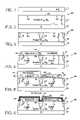
- FIG. 1is a schematic cross section view of a portion of a semiconductor substrate base.
- FIG. 2is the semiconductor substrate of FIG. 1 after forming a layer of graded silicon germanium material on the substrate.
- FIG. 3shows the semiconductor substrate of FIG. 2 after forming an electronically insulating material between areas of the graded silicon germanium material.
- FIG. 4shows the semiconductor substrate of FIG. 1 after selective deposition of a layer of silicon material over a first area of the graded silicon germanium material.
- FIG. 5shows the semiconductor substrate of FIG. 1 after selective deposition of a layer of silicon germanium material over a second area of the graded silicon germanium material, where the silicon germanium material has a higher concentration of germanium than the graded silicon germanium material has at the second area.
- FIG. 6shows the semiconductor substrate of FIG. 1 after forming a layer of high dielectric constant material over the selectively deposited silicon and the selectively deposited silicon germanium material.
- FIG. 7shows the semiconductor substrate of FIG. 1 after forming an NMOS device in the selectively deposited silicon material, and a PMOS device in the selectively deposited silicon germanium material.
- FIG. 1is a schematic cross section view of a portion of a semiconductor substrate base.
- silicon base 110may include, be formed from, or grown from poly-crystal silicon, single crystal silicon, or various other suitable technologies for forming a silicon base or substrate, such as a silicon wafer.
- base 110may be formed by growing a single crystal silicon substrate base material having thickness H 0 of between 100 angstroms and 1,000 angstroms of pure silicon.
- FIG. 2is the semiconductor substrate of FIG. 1 after forming a layer of graded silicon germanium (SiGe) material on the substrate.
- FIG. 2shows substrate material 120 of graded silicon germanium formed on top of substrate base 110 .
- substrate material 120may be a layer of graded relaxed silicon alloy material formed by chemical vapor deposition (CVD) epitaxial growth of graded relaxed SiGe in a chamber, such as a semiconductor device fabrication chamber.
- CVDchemical vapor deposition
- such CVD growthmay be accomplished by placing substrate base 110 into the chamber, heating the inside of the chamber to a temperature between 500° Celsius and 1,000° Celsius in a hydrogen ambient flow (H 2 ) of between 5 standard liters per minute (SLM) and 50 SLM, pressurizing the chamber to a pressure between 10 Torr and 200 Torr (e.g., such as either by atmospheric or reduced pressure), flowing into the chamber a silicon precursor (e.g., such as the silicon precursor described herein) at a flow into the chamber of between 50 SCCM and 500 SCCM, and slowly increasing a flow of germanium precursor from 0 SCCM to a final value sufficient to cause upper surface 129 to have a percentage of germanium between 10% and 35% germanium.
- H 2hydrogen ambient flow
- SLMstandard liters per minute
- the flow of germanium precursormay be increased sufficiently to cause a grading of germanium from 0% initial concentration of germanium, such as at lower surface 121 , to increase to between 20 and 30% final concentration germanium, such as at upper surface 129 at for instance, a grading rate of change of germanium concentration of 10% germanium per micrometer in depth (e.g., such as per micrometer in depth of thickness H 3 ).
- substrate material 120may have a concentration of germanium, such as at upper surface 129 , of between 5 and 20% final concentration germanium.
- the grading rate, and/or thickness of the graded silicon germanium materialmay be varied to provide a selected final concentration of germanium at upper surface 129 resulting from a selected grading rate initiated at lower surface 121 .
- the grading ratemay be established by a continuous change in grading, a linear change in grading, a non-linear change in grading, and/or a step-grading change of germanium concentration in substrate material 120 .
- the flow of germanium precursorcan be increased so that the grading rate increases smoothly and continuously, or so that the grading rate has an abrupt step-grading change of germanium concentration in substrate material 120 of between 1% and 2% increments every 1,000 to 2,000 angstroms.
- the initial flow of germanium precursor, increase in flow of germanium precursor, and final flow of germanium precursormay be selected and may vary widely depending on the desired final target concentration of germanium in substrate material 120 (e.g., such as at upper surface 129 ), the temperature used during formation, and the concentration of the germanium precursor.
- the germanium precursormay be germane (GeH 4 ) and may be increased in flow linearly, or non-linearly versus time to achieve a selected grading profile, and may be increased to a final flow value sufficient to cause upper surface 129 to have a selected percentage of germanium.
- the germanium precursormay be a germane precursor diluted in H 2 , or may be pure germane increased to a final flow at or below 100 SCCM. In fact, it is possible to increase the flow of germanium precursor to grow a relaxed graded film of silicon germanium with up to 100% germanium at upper surface 129 .
- substrate material 120may be graded relaxed silicon germanium material having a grading concentration that increases from 0% at lower surface 121 to between 10% and 30% at upper surface 129 , at a rate of between 5% and 15% increase in germanium per micrometer in depth (e.g., such as in depth related to thickness H 3 ).
- Graded relaxed silicon germaniumincludes graded silicon germanium in a “relaxed” status such as where the alignment of silicon and germanium molecules in the SiGe structure (substrate base 110 plus substrate material 120 ) have relatively few dislocations, even where the percentage of Ge grading increases (e.g., such as increasing via smooth or step grading).
- forming graded relaxed silicon germaniummay include flowing between 50 SCCM and 100 SCCM of HCl during CVD epitaxial growth of substrate material 120 .
- a sufficient amount of HClmay be introduced during formation of substrate material 120 to increase or improve the planarity of upper surface 129 , to reduce or control so-called “cross-hatch” that develops during relaxed silicon germanium growth (e.g., such as to reduce the crisscross strain or grid pattern in or at upper surface 129 that may be attributed to relaxation of silicon germanium molecules during deposition).
- substrate material 120is described above as being formed of graded silicon germanium, substrate material 120 may be formed by CVD epitaxial growth, ultrahigh vacuum (UHV) CVD epitaxial growth, and/or molecular beam epitaxy (MBE) epitaxial growth of various appropriate silicon alloys (e.g., such as silicon germanium).
- substrate material 120may be formed by sufficient CVD of various appropriate silicon alloy materials to form a graded relaxed layer of silicon alloy material having a thickness between 1 and 3 micrometers in thickness, such as by CVD of silicon germanium to form graded substrate material 120 having a thickness H 3 of 2 micrometers in thickness.
- substrate material 120may be formed by an appropriate layer transfer/bonding techniques, such as a substrate SiGe On Insulator (SGOI) process where a relaxed SiGe substrate is prepared by growing SiGe on a bulk substrate by an appropriate process and then transferring a relaxed top layer of the SiGe to a different substrate (e.g., such as to substrate base 110 , which may be a silicon oxide wafer) to form substrate material 120 .
- substrate material 120may be non-graded silicon alloy material.
- FIG. 2also shows substrate material 120 having first area 123 and second area 125 of upper surface 129 , which are suitable for depositing a transistor device semiconductor channel material onto.
- FIG. 3shows the semiconductor substrate of FIG. 2 after forming an electronically insulating material between areas of the graded silicon germanium material.
- FIG. 3shows shallow trench isolation (STI) material 130 between first area 123 and second area 125 .
- STIshallow trench isolation
- FIG. 3shows STI material 130 between first area 123 and second area 125
- various appropriate electronically insulating materials and structures sufficient for isolating a P-type well of a CMOS device from an N-type well of the CMOS deviceare contemplated.
- substrate material 120may be doped at first area 123 with one of boron and aluminum to form a P-type well region 122 having an electrically positive charge, such as for a an NMOS transistor of a CMOS device.
- substrate material 120may be doped at second area 125 with phosphorous, arsenic, and/or antimony to form N-type well region 124 having an electrically negative charge, such as for a PMOS transistor of a CMOS device.
- a maskmay be placed over the non selected area to block the introduction of deposit into the non selected area.
- a layer of silicon material having a thickness suitable as a first channel for a first circuit device on first area 123 of substrate material 120may be formed to define a first interface surface of substrate material 120 .
- a layer of silicon germanium material suitable as a second channel for a second circuit device on second area 125 of substrate material 120may be formed to define a second interface surface of substrate material 120 .
- FIG. 4shows the semiconductor substrate of FIG. 1 after selective deposition of a layer of silicon material over a first area of the graded silicon germanium material.
- FIG. 4shows first dielectric layer 140 formed over second area 125 of substrate material 120 .
- first dielectric layer 140may be formed of a material such as an etch stop and/or dielectric material, including silicon dioxide (SiO 2 ), silicon nitride (Si 3 N 4 ), an etch stop dielectric, or other suitable dielectric.
- etch stop and/or dielectric materialincluding silicon dioxide (SiO 2 ), silicon nitride (Si 3 N 4 ), an etch stop dielectric, or other suitable dielectric.
- first layer 150may be formed over first area 123 of substrate material 120 .
- first layer 150is an epitaxial layer of silicon material formed by selective CVD epitaxial growth of tensile strained silicon, such as a layer of silicon experiencing a tensile strain in directions of arrows 152 and 154 caused by a lattice spacing of the silicon material being smaller than a lattice spacing of the relaxed graded silicon germanium substrate material 120 at first area 123 .
- Selective CVD epitaxial growth of the silicon layermay include placing structure 400 without first layer 150 , into a chamber, heating the inside of the chamber to a temperature between 600° Celsius and 900° Celsius in a hydrogen ambient flow (H 2 ) of between 5 SLM and 50 SLM, pressurizing the chamber to a pressure between 10 Torr and 200 Torr (e.g., such as by pressurizing either to atmospheric or reduced pressure), and flowing into the chamber a silicon precursor at a flow of between 50 SCCM and 500 SCCM to form an epitaxial layer of silicon material having a thickness H 1 between 10 nano-meters and 20 nano-meters in thickness.
- H 2hydrogen ambient flow
- first layer 150may have a thickness sufficient to avoid dislocations, misfits, or threaded dislocations between first layer 150 and substrate material 120 at a first interface defined where first layer 150 is coupled to upper surface 129 of substrate material 120 at first area 123 .
- first layer 150may include flowing dichlorosilane (SiH 2 Cl 2 ) to selectively deposit silicon material having a thickness H 1 of between 100 angstroms and 1,000 angstroms of pure silicon. Moreover, it is contemplated that forming of first layer 150 may include introducing between 50 SCCM and 500 SCCM of HCl, such as by flowing HCl during selective CVD epitaxial growth of tensile strain silicon (e.g., such as is described above with respect to forming substrate material 120 ).
- dichlorosilaneSiH 2 Cl 2
- forming of first layer 150may include introducing between 50 SCCM and 500 SCCM of HCl, such as by flowing HCl during selective CVD epitaxial growth of tensile strain silicon (e.g., such as is described above with respect to forming substrate material 120 ).
- first layer 150is described above as being formed by CVD epitaxial growth, first layer 150 may be formed by other appropriate processes including UHV CVD epitaxial growth, SGOI, and/or MBE epitaxial growth, such as those described herein, to form a layer of silicon.
- first layer 150may include various other appropriate silicon material that will experience a tensile strain when formed on first area 123 .
- a second dielectric layermay be formed over first layer 150 , and then a layer of silicon germanium material suitable as a second channel for a second circuit device may be formed on second area 125 of substrate material 120 .
- FIG. 5shows the semiconductor substrate of FIG. 1 after selective deposition of a layer of silicon germanium material over a second area of the graded silicon germanium material, where the silicon germanium material has a higher concentration of germanium than the graded silicon germanium material has at the second area.
- FIG. 5shows different second layer 160 suitable as a second channel for a second circuit device formed on second area 125 of graded silicon germanium substrate material 120 , and second dielectric layer 142 conformally formed over first layer 150 at first area 123 .
- second dielectric layer 142may be formed of a material, by a process, and to a thickness, such as described above for first dielectric layer 140 .
- second dielectric layer 142may be conformally deposited over the surface of first layer 150 in that the thickness of second dielectric layer 142 is consistent throughout and conforms to the topography of the surface of first layer 150 .
- FIG. 5shows second layer 160 , such as an epitaxial layer of silicon alloy material that may be formed by selective CVD epitaxial growth of compressive strained silicon germanium.
- second layer 160may be formed by selective CVD epitaxial growth by placing structure 500 without second layer 160 into a chamber, heating the chamber inside to a temperature between 500° Celsius and 800° Celsius in a hydrogen ambient flow (H 2 ) of between 5 SLM and 50 SLM, pressurizing the chamber to a pressure between 10 Torr and 200 Torr (e.g., such as pressurizing to atmospheric or reduced pressure), flowing into the chamber a silicon precursor at a flow rate of between 50 SCCM and 500 SCCM, and flowing into the chamber a germanium precursor at a flow rate of up to 100 SCCM (undiluted) to cause second layer 160 to have a percentage of germanium between 20% and 60%.
- H 2hydrogen ambient flow
- second layer 160may be formed, such as with a sufficient percentage of germanium, to cause second layer 160 to experience a compressive strain in directions of arrows 162 and 164 due to a lattice spacing of epitaxial layer of silicon alloy material being larger than a lattice spacing of graded silicon germanium substrate material 120 at second area 125 .
- formation of second layer 160can include flowing a germanium precursor at a rate such that second layer 160 is an epitaxial layer of silicon germanium material having a thickness H 2 of between 10 nano-meters and 20 nano-meters in thickness. Therefore, second layer 160 may have a thickness sufficient to avoid dislocations, misfits, or threaded dislocations at a second interface defined by where second layer 160 is coupled to upper surface 129 of substrate material 120 at second area 125 .
- flowing a silicon precursor for forming second layer 160may include flowing a precursor and/or flowing at a rate such as is described above with respect to flowing a silicon precursor to form substrate base 110 and first layer 150 .
- the silicon precursor described above for forming second layer 160may be dichlorosilane (SiH 2 Cl 2 ) flown at a rate sufficient so that when combined with the flowing of the germanium precursor, a silicon germanium material may be formed to provide second layer 160 having thickness H 2 of between 100 angstroms and 1,000 angstroms of silicon germanium material.
- flowing of a germanium precursor described above with respect to forming second layer 160may include flowing a germanium precursor and/or flowing a germanium precursor at a flow rate as described above with respect to flowing a germanium precursor to form graded silicon germanium substrate material 120 .
- flowing a germanium precursor to form second layer 160may include flowing germane (GeH 4 ) sufficiently to cause second layer 160 to have a selected percentage of germanium and a selected thickness (e.g., such as by flowing germane as described above with respect to forming graded silicon germanium substrate material 120 in FIG. 2 ).
- second layer 160may include introducing between 50 SCCM and 500 SCCM of HCl, such as is described above with respect to forming first layer 150 at FIG. 4 .
- second layer 160may be formed by CVD epitaxial growth, UHV CVD epitaxial growth, SGOI, and/or MBE epitaxial growth of various appropriate silicon alloys (e.g., such as silicon germanium).
- dopingcan be done in a “self-aligned” manner, such as a manner without additional masking.
- first dielectric 140 shown in FIG. 4may be deposited over wafer 300 of FIG. 3 (e.g., including first area 123 and second area 125 ).
- resiste.g., such as a photoresist
- first dielectric 140is etched to expose the first area 123 over P-well 122 .
- ion implantationcan be performed to dope P-well 122 (e.g., such as with dopants as described above for doping first area 123 ).
- the remaining resistis stripped from wafer 300 and first layer 150 is selectively deposited as shown in FIG. 4 .
- a similar processcan be used when forming second dielectric 142 and second layer 160 , to dope second area 125 (e.g., such as with dopants as described above for doping second area 125 ), and resulting in the structure shown in FIG. 5 . It can be appreciated that the order of certain “self-aligned” doping processes mentioned above can be reversed.
- the channel SiGe materialmay form a coherent alignment with the graded relaxed substrate material SiGe (e.g., such as at second area 125 of substrate material 120 ; where substrate material 120 may also be in coherent alignment within the graded substrate, such as along thickness H 3 ), but will experience compressive strains 162 and 164 because of the jump in percentage in Ge between the channel material and the substrate material, at the substrate/channel interface (e.
- first layer 150 and/or second layer 160may be formed after formation of electronically isolating regions between first area 123 and second area 125 (e.g., such as prior to forming STI material 130 ) so that high temperature processes for forming electronically isolating regions will not be a factor in reducing selected thickness of or in inducing relaxation of a tensile strain in first layer 150 and/or a compressive strain in second layer 160 .
- first layer 150 and/or second layer 160 on first area 123 and second area 125may include a size of first area 123 and a size of second area 125 selected to be small enough to increase or provide sufficient stability of first layer 150 to allow tensile strain deposition on a buffer of relaxed graded silicon germanium substrate material 120 with a selected percentage of germanium at first area 123 , as well as to allow compressive strained deposition of second layer 160 on a buffer of relaxed graded silicon germanium substrate material 120 having a selected percentage of germanium at second area 125 which is approximately equal to the percentage of germanium at first area 123 .
- first layer 150may be doped with boron and/or aluminum to form a P-type channel region having an electrically positive charge, (e.g., see first dielectric layer 140 above) and second layer 160 may be doped with phosphorous, arsenic, and/or antimony to form an N-type channel region having an electrically negative charge.
- first layer 150 and/or second layer 160may be doped by introducing the dopants identified above during deposition of, or doping with the dopants identified above after deposition of first layer 150 and/or second layer 160 .
- first layer 150 and/or second layer 160may be doped with a sufficient amount of an appropriate type of dopant to form a P-type channel region and/or a P-type channel region, respectively, such as for a NMOS and/or PMOS device, respectively, such as for a CMOS circuit.
- first layer 150 and/or second layer 160may be doped with between 1.0 exponential to the 17th and 1.0 exponential to the 18th of dopant particles per cubic centimeter of channel material.
- dopingmay be performed with less than an amount of dopant particles that would result in degraded carrier mobility due to excessive impurity scattering.
- a third dielectric layermay be formed over first layer 150 and different second layer 160 .
- FIG. 6shows the semiconductor substrate of FIG. 1 after forming a layer of high dielectric constant material over the selectively deposited silicon and the selectively deposited silicon germanium material.
- FIG. 6shows third dielectric layer 144 , such as a layer of dielectric material having a relatively high dielectric constant (e.g. “a high K dielectric”, having a K greater than or equal to 3.9 and/or the K of silicon dioxide (SiO 2 )), which may be between 2 and 4 nano-meters in thickness, formed over first layer 150 and second layer 160 .
- a relatively high dielectric constante.g. “a high K dielectric”, having a K greater than or equal to 3.9 and/or the K of silicon dioxide (SiO 2 )
- Third dielectric layer 144may be formed by atomic layer deposition (ALD) such as by ALD of silicon dioxide (SiO 2 ), hafnium oxide (HfO), hafnium silicate (HfSiO 4 ), hafnium disilicate (HfSi 4 O 7 ), zirconium oxide (ZrO), zirconium silicate (ZrSiO 4 ), tantalum oxide (Ta 2 O 5 ).
- ALDatomic layer deposition
- FIG. 7shows the semiconductor substrate of FIG. 1 after forming an NMOS device in the selectively deposited silicon material, and a PMOS device in the selectively deposited silicon germanium material.
- FIG. 7shows first layer 150 doped to form P-type channel region 176 , and second layer 160 doped to form N-type channel region 186 .
- FIG. 7also shows NMOS device 178 having N-type gate electrode 170 on a surface of third dielectric layer 144 over first layer 150 (e.g., N-type gate electrode 170 having an electrically negative charge), N-type first junction region 172 and second junction region 174 in first layer 150 adjacent to N-type gate electrode 170 (e.g., such as N-type first junction region 172 and second junction region 174 having an electrically negative charge).
- FIG. 7also shows NMOS spacers 712 and 714 formed on surfaces of N-type gate electrode 170 .
- PMOS device 188having P-type gate electrode 180 on a surface of third dielectric layer 144 over second layer 160 (e.g., such as wherein P-type gate electrode 180 has an electrically positive charge), and P-type first junction region 182 and P-type second junction region 184 in second layer 160 adjacent P-type gate electrode 180 (e.g., such as where P-type first junction region 182 and second junction region 184 have an electrically positive charge).
- FIG. 7also shows PMOS spacers 412 and 414 formed on surfaces of P-type gate electrode 180 .
- first layer 150may be formed suitable as P-type channel region 176 for NMOS device 178 on first area 123 of substrate material 120 , first layer 150 having a first material with a first lattice spacing different (e.g., such as smaller) than a substrate lattice spacing of a substrate material defining a first interface surface of the substrate (e.g., such as at first area 123 ).
- second layer 160may be formed suitable as N-type channel region 186 for PMOS device 188 on a different second area 125 of substrate material 120 , second layer 160 having a different second material with a second lattice spacing different than the first lattice spacing of the first layer and different than the substrate lattice spacing of the substrate material (e.g., such as by the second lattice spacing having a larger lattice spacing than the substrate material), where the second layer defines a second interface surface of the substrate (e.g., such as at second area 125 ).
- the difference between the first lattice spacing of first layer 150 and the substrate lattice spacing at first area 123may define a tensile strain in the direction of arrows 152 and 154 in first layer 150 , which is sufficient to enhance or increase electron mobility in first layer 150 (e.g., such as by at least 50, 75, 80, or 85 percent).
- the difference between the second lattice spacing of second layer 160 and the substrate lattice spacing at second area 125may define a compressive strain in the direction shown by arrows 162 and 164 in second layer 160 , which is sufficient to enhance or increase hole mobility in second layer 160 (e.g., such as by at least 50, 80, 90, 100, or 110 percent).
- the tensile strain in first layer 150may be a bi-axial tensile strain such as to stretch or expand first layer 150 outward in the direction of arrows 152 and 154 , as well as in the direction of an arrow pointing towards the viewer and away from the cross sectional surface of first layer 150 shown in FIGS. 5-7 .
- the compressive strain in second layer 160may be a bi-axial compressive strain such as to contract or squeeze second layer 160 inward in the direction of arrows 162 and 164 , as well as in the direction of an arrow pointing away from the viewer and towards the cross sectional surface of second layer 160 shown in FIGS. 5-7 .
- the thickness of substrate material 120 , and concentration of germanium at upper surface 129 , thickness of first layer 150 , thickness of second layer 160 and percentage of germanium in second layer 160may be selected as described herein so that a two dimensional coherent tensile strain is induced in first layer 150 from bonding of first layer 150 at first area 123 to substrate material 120 (e.g., such as a coherent strain caused by the atomic structure of the material of first layer 150 lining up with the atomic structure of substrate material 120 at first area 123 , even though the material of first layer 150 has a lattice alignment of a smaller lattice spacing than that of first area 123 ).
- a two dimensional coherent compressive strainis induced in second layer 160 from bonding of second layer 160 to substrate material 120 at second area 125 (e.g., such as a coherent strain caused by the atomic structure of the material of second layer 160 lining up with the atomic structure of substrate material 120 at second area 125 , even though the material of second layer 160 has a lattice alignment of a larger lattice spacing than that of second area 125 ).
- Xmay be less than Y.
- Xmay be between 0.1 and 0.3, while Y is between 0.2 and 0.6.
- Ymay be between 0.1 and 0.3 larger than X.
- Xmay be 0.2 and Y may be 0.5.
Landscapes
- Engineering & Computer Science (AREA)
- Microelectronics & Electronic Packaging (AREA)
- Condensed Matter Physics & Semiconductors (AREA)
- General Physics & Mathematics (AREA)
- Manufacturing & Machinery (AREA)
- Computer Hardware Design (AREA)
- Physics & Mathematics (AREA)
- Power Engineering (AREA)
- Chemical & Material Sciences (AREA)
- Materials Engineering (AREA)
- Insulated Gate Type Field-Effect Transistor (AREA)
- Metal-Oxide And Bipolar Metal-Oxide Semiconductor Integrated Circuits (AREA)
- Recrystallisation Techniques (AREA)
- Element Separation (AREA)
Abstract
Description
Circuit devices and the manufacture and structure of circuit devices.
Increased performance of circuit devices on a substrate (e.g., integrated circuit (IC) transistors, resistors, capacitors, etc. on a semiconductor (e.g., silicon) substrate) is typically a major factor considered during design, manufacture, and operation of those devices. For example, during design and manufacture or forming of metal oxide semiconductor (MOS) transistor semiconductor devices, such as those used in a complementary metal oxide semiconductor (CMOS), it is often desired to increase movement of electrons in N-type MOS device (NMOS) channels and to increase movement of positive charged holes in P-type MOS device (PMOS) channels.
The embodiments of the invention are illustrated by way of example and not by way of limitation in the figures of the accompanying drawings in which like references indicate similar elements. It should be noted that references to “an” embodiment of the invention in this disclosure are not necessarily to the same embodiment, and they mean at least one.
Thus, according to embodiments, the grading rate, and/or thickness of the graded silicon germanium material may be varied to provide a selected final concentration of germanium atupper surface 129 resulting from a selected grading rate initiated atlower surface 121. Moreover, according to embodiments, the grading rate may be established by a continuous change in grading, a linear change in grading, a non-linear change in grading, and/or a step-grading change of germanium concentration insubstrate material 120. Specifically, for example, the flow of germanium precursor can be increased so that the grading rate increases smoothly and continuously, or so that the grading rate has an abrupt step-grading change of germanium concentration insubstrate material 120 of between 1% and 2% increments every 1,000 to 2,000 angstroms. Additionally, according to embodiments, the initial flow of germanium precursor, increase in flow of germanium precursor, and final flow of germanium precursor may be selected and may vary widely depending on the desired final target concentration of germanium in substrate material120 (e.g., such as at upper surface129), the temperature used during formation, and the concentration of the germanium precursor.
For instance, in one embodiment, the germanium precursor may be germane (GeH4) and may be increased in flow linearly, or non-linearly versus time to achieve a selected grading profile, and may be increased to a final flow value sufficient to causeupper surface 129 to have a selected percentage of germanium. Also, the germanium precursor may be a germane precursor diluted in H2, or may be pure germane increased to a final flow at or below 100 SCCM. In fact, it is possible to increase the flow of germanium precursor to grow a relaxed graded film of silicon germanium with up to 100% germanium atupper surface 129.
Likewise, according to embodiments,substrate material 120 may be graded relaxed silicon germanium material having a grading concentration that increases from 0% atlower surface 121 to between 10% and 30% atupper surface 129, at a rate of between 5% and 15% increase in germanium per micrometer in depth (e.g., such as in depth related to thickness H3). Graded relaxed silicon germanium, includes graded silicon germanium in a “relaxed” status such as where the alignment of silicon and germanium molecules in the SiGe structure (substrate base 110 plus substrate material120) have relatively few dislocations, even where the percentage of Ge grading increases (e.g., such as increasing via smooth or step grading).
Also, according to embodiments, forming graded relaxed silicon germanium may include flowing between 50 SCCM and 100 SCCM of HCl during CVD epitaxial growth ofsubstrate material 120. For example, a sufficient amount of HCl may be introduced during formation ofsubstrate material 120 to increase or improve the planarity ofupper surface 129, to reduce or control so-called “cross-hatch” that develops during relaxed silicon germanium growth (e.g., such as to reduce the crisscross strain or grid pattern in or atupper surface 129 that may be attributed to relaxation of silicon germanium molecules during deposition). Furthermore, according to embodiments, althoughsubstrate material 120 is described above as being formed of graded silicon germanium,substrate material 120 may be formed by CVD epitaxial growth, ultrahigh vacuum (UHV) CVD epitaxial growth, and/or molecular beam epitaxy (MBE) epitaxial growth of various appropriate silicon alloys (e.g., such as silicon germanium). Thus, for example,substrate material 120 may be formed by sufficient CVD of various appropriate silicon alloy materials to form a graded relaxed layer of silicon alloy material having a thickness between 1 and 3 micrometers in thickness, such as by CVD of silicon germanium to form gradedsubstrate material 120 having a thickness H3 of 2 micrometers in thickness. Moreover,substrate material 120 may be formed by an appropriate layer transfer/bonding techniques, such as a substrate SiGe On Insulator (SGOI) process where a relaxed SiGe substrate is prepared by growing SiGe on a bulk substrate by an appropriate process and then transferring a relaxed top layer of the SiGe to a different substrate (e.g., such as tosubstrate base 110, which may be a silicon oxide wafer) to formsubstrate material 120. It is also considered thatsubstrate material 120 may be non-graded silicon alloy material.
Next, according to embodiments,substrate material 120 may be doped atfirst area 123 with one of boron and aluminum to form a P-type well region 122 having an electrically positive charge, such as for a an NMOS transistor of a CMOS device. Similarly,substrate material 120 may be doped atsecond area 125 with phosphorous, arsenic, and/or antimony to form N-type well region 124 having an electrically negative charge, such as for a PMOS transistor of a CMOS device. To selectively dopefirst area 123 andsecond area 125, a mask may be placed over the non selected area to block the introduction of deposit into the non selected area.
After P-type well region 122 and N-type well region 124 are formed insubstrate material 120, a layer of silicon material having a thickness suitable as a first channel for a first circuit device onfirst area 123 ofsubstrate material 120 may be formed to define a first interface surface ofsubstrate material 120. In addition, a layer of silicon germanium material suitable as a second channel for a second circuit device onsecond area 125 ofsubstrate material 120 may be formed to define a second interface surface ofsubstrate material 120. For example,FIG. 4 shows the semiconductor substrate ofFIG. 1 after selective deposition of a layer of silicon material over a first area of the graded silicon germanium material.FIG. 4 shows firstdielectric layer 140 formed oversecond area 125 ofsubstrate material 120. According to embodiments, firstdielectric layer 140 may be formed of a material such as an etch stop and/or dielectric material, including silicon dioxide (SiO2), silicon nitride (Si3N4), an etch stop dielectric, or other suitable dielectric.
After forming firstdielectric layer 140,first layer 150 may be formed overfirst area 123 ofsubstrate material 120. For example, as shown inFIG. 4 ,first layer 150 is an epitaxial layer of silicon material formed by selective CVD epitaxial growth of tensile strained silicon, such as a layer of silicon experiencing a tensile strain in directions ofarrows germanium substrate material 120 atfirst area 123. Selective CVD epitaxial growth of the silicon layer may include placingstructure 400 withoutfirst layer 150, into a chamber, heating the inside of the chamber to a temperature between 600° Celsius and 900° Celsius in a hydrogen ambient flow (H2) of between 5 SLM and 50 SLM, pressurizing the chamber to a pressure between 10 Torr and 200 Torr (e.g., such as by pressurizing either to atmospheric or reduced pressure), and flowing into the chamber a silicon precursor at a flow of between 50 SCCM and 500 SCCM to form an epitaxial layer of silicon material having a thickness H1 between 10 nano-meters and 20 nano-meters in thickness. For example,first layer 150 may have a thickness sufficient to avoid dislocations, misfits, or threaded dislocations betweenfirst layer 150 andsubstrate material 120 at a first interface defined wherefirst layer 150 is coupled toupper surface 129 ofsubstrate material 120 atfirst area 123.
More particularly, formingfirst layer 150 may include flowing dichlorosilane (SiH2Cl2) to selectively deposit silicon material having a thickness H1 of between 100 angstroms and 1,000 angstroms of pure silicon. Moreover, it is contemplated that forming offirst layer 150 may include introducing between 50 SCCM and 500 SCCM of HCl, such as by flowing HCl during selective CVD epitaxial growth of tensile strain silicon (e.g., such as is described above with respect to forming substrate material120). Furthermore, according to embodiments, althoughfirst layer 150 is described above as being formed by CVD epitaxial growth,first layer 150 may be formed by other appropriate processes including UHV CVD epitaxial growth, SGOI, and/or MBE epitaxial growth, such as those described herein, to form a layer of silicon.
Also, according to embodiments,first layer 150 may include various other appropriate silicon material that will experience a tensile strain when formed onfirst area 123.
After formingfirst layer 150, a second dielectric layer may be formed overfirst layer 150, and then a layer of silicon germanium material suitable as a second channel for a second circuit device may be formed onsecond area 125 ofsubstrate material 120. For example,FIG. 5 shows the semiconductor substrate ofFIG. 1 after selective deposition of a layer of silicon germanium material over a second area of the graded silicon germanium material, where the silicon germanium material has a higher concentration of germanium than the graded silicon germanium material has at the second area.FIG. 5 shows differentsecond layer 160 suitable as a second channel for a second circuit device formed onsecond area 125 of graded silicongermanium substrate material 120, and seconddielectric layer 142 conformally formed overfirst layer 150 atfirst area 123. According to embodiments, seconddielectric layer 142 may be formed of a material, by a process, and to a thickness, such as described above for firstdielectric layer 140. For example, seconddielectric layer 142 may be conformally deposited over the surface offirst layer 150 in that the thickness of seconddielectric layer 142 is consistent throughout and conforms to the topography of the surface offirst layer 150.
In particular,FIG. 5 showssecond layer 160, such as an epitaxial layer of silicon alloy material that may be formed by selective CVD epitaxial growth of compressive strained silicon germanium. For example,second layer 160 may be formed by selective CVD epitaxial growth by placingstructure 500 withoutsecond layer 160 into a chamber, heating the chamber inside to a temperature between 500° Celsius and 800° Celsius in a hydrogen ambient flow (H2) of between 5 SLM and 50 SLM, pressurizing the chamber to a pressure between 10 Torr and 200 Torr (e.g., such as pressurizing to atmospheric or reduced pressure), flowing into the chamber a silicon precursor at a flow rate of between 50 SCCM and 500 SCCM, and flowing into the chamber a germanium precursor at a flow rate of up to 100 SCCM (undiluted) to causesecond layer 160 to have a percentage of germanium between 20% and 60%. Thus,second layer 160 may be formed, such as with a sufficient percentage of germanium, to causesecond layer 160 to experience a compressive strain in directions ofarrows germanium substrate material 120 atsecond area 125. Specifically, formation ofsecond layer 160 can include flowing a germanium precursor at a rate such thatsecond layer 160 is an epitaxial layer of silicon germanium material having a thickness H2 of between 10 nano-meters and 20 nano-meters in thickness. Therefore,second layer 160 may have a thickness sufficient to avoid dislocations, misfits, or threaded dislocations at a second interface defined by wheresecond layer 160 is coupled toupper surface 129 ofsubstrate material 120 atsecond area 125.
It can be appreciated that flowing a silicon precursor for formingsecond layer 160 may include flowing a precursor and/or flowing at a rate such as is described above with respect to flowing a silicon precursor to formsubstrate base 110 andfirst layer 150. More particularly, for example, the silicon precursor described above for formingsecond layer 160 may be dichlorosilane (SiH2Cl2) flown at a rate sufficient so that when combined with the flowing of the germanium precursor, a silicon germanium material may be formed to providesecond layer 160 having thickness H2 of between 100 angstroms and 1,000 angstroms of silicon germanium material. Likewise, flowing of a germanium precursor described above with respect to formingsecond layer 160 may include flowing a germanium precursor and/or flowing a germanium precursor at a flow rate as described above with respect to flowing a germanium precursor to form graded silicongermanium substrate material 120. Specifically, for instance, flowing a germanium precursor to formsecond layer 160 may include flowing germane (GeH4) sufficiently to causesecond layer 160 to have a selected percentage of germanium and a selected thickness (e.g., such as by flowing germane as described above with respect to forming graded silicongermanium substrate material 120 inFIG. 2 ).
Moreover, it is contemplated that formingsecond layer 160 may include introducing between 50 SCCM and 500 SCCM of HCl, such as is described above with respect to formingfirst layer 150 atFIG. 4 . Furthermore, according to embodiments, althoughsecond layer 160 is described above as being formed of graded silicon germanium,second layer 160 may be formed by CVD epitaxial growth, UHV CVD epitaxial growth, SGOI, and/or MBE epitaxial growth of various appropriate silicon alloys (e.g., such as silicon germanium).
In addition to the doping atfirst area 123 andsecond area 125 described above, according to embodiments doping can be done in a “self-aligned” manner, such as a manner without additional masking. For instance,first dielectric 140 shown inFIG. 4 may be deposited overwafer 300 ofFIG. 3 (e.g., includingfirst area 123 and second area125). Then, resist (e.g., such as a photoresist) may be spun and exposed over P-well 122. The resist is then removed andfirst dielectric 140 is etched to expose thefirst area 123 over P-well 122. Next, ion implantation can be performed to dope P-well122 (e.g., such as with dopants as described above for doping first area123). The remaining resist is stripped fromwafer 300 andfirst layer 150 is selectively deposited as shown inFIG. 4 . Moreover, a similar process can be used when formingsecond dielectric 142 andsecond layer 160, to dope second area125 (e.g., such as with dopants as described above for doping second area125), and resulting in the structure shown inFIG. 5 . It can be appreciated that the order of certain “self-aligned” doping processes mentioned above can be reversed.
Also, according to embodiments, a distinction is drawn with respect to the increasing percentage or grading concentration of germanium in the relaxed silicon germanium substrate material (e.g., such assubstrate material 120 having a percentage of Ge increase such as a percentage of Ge increasing via smooth or step grading) and the sudden increase in germanium at an interface between the graded relaxed silicon germanium substrate material and the channel SiGe (e.g., such as the sudden increase betweensecond layer 160 which has a greater percentage of Ge atsecond area 125 thansubstrate material 120 by, for example, between 10 percent and 30 percent.) Thus, the channel SiGe material (e.g., second layer160) may form a coherent alignment with the graded relaxed substrate material SiGe (e.g., such as atsecond area 125 ofsubstrate material 120; wheresubstrate material 120 may also be in coherent alignment within the graded substrate, such as along thickness H3), but will experiencecompressive strains second area 125 contacts second layer160). Furthermore, although descriptions above for formingsecond layer 160 are focused on forming a layer of silicon germanium, according to embodiments,second layer 160 may be formed of various appropriate silicon alloy materials, such as by selective epitaxial CVD of such a material.
It is noted thatfirst layer 150 and/orsecond layer 160 may be formed after formation of electronically isolating regions betweenfirst area 123 and second area125 (e.g., such as prior to forming STI material130) so that high temperature processes for forming electronically isolating regions will not be a factor in reducing selected thickness of or in inducing relaxation of a tensile strain infirst layer 150 and/or a compressive strain insecond layer 160. Moreover, it is appreciated that selective formation offirst layer 150 and/orsecond layer 160 onfirst area 123 andsecond area 125 may include a size offirst area 123 and a size ofsecond area 125 selected to be small enough to increase or provide sufficient stability offirst layer 150 to allow tensile strain deposition on a buffer of relaxed graded silicongermanium substrate material 120 with a selected percentage of germanium atfirst area 123, as well as to allow compressive strained deposition ofsecond layer 160 on a buffer of relaxed graded silicongermanium substrate material 120 having a selected percentage of germanium atsecond area 125 which is approximately equal to the percentage of germanium atfirst area 123.
Also,first layer 150 may be doped with boron and/or aluminum to form a P-type channel region having an electrically positive charge, (e.g., see firstdielectric layer 140 above) andsecond layer 160 may be doped with phosphorous, arsenic, and/or antimony to form an N-type channel region having an electrically negative charge. For example,first layer 150 and/orsecond layer 160 may be doped by introducing the dopants identified above during deposition of, or doping with the dopants identified above after deposition offirst layer 150 and/orsecond layer 160. Thus,first layer 150 and/orsecond layer 160 may be doped with a sufficient amount of an appropriate type of dopant to form a P-type channel region and/or a P-type channel region, respectively, such as for a NMOS and/or PMOS device, respectively, such as for a CMOS circuit. Specifically, for example,first layer 150 and/orsecond layer 160 may be doped with between 1.0 exponential to the 17th and 1.0 exponential to the 18th of dopant particles per cubic centimeter of channel material. Thus, such doping may be performed with less than an amount of dopant particles that would result in degraded carrier mobility due to excessive impurity scattering.
After formation ofsecond layer 160, a third dielectric layer may be formed overfirst layer 150 and differentsecond layer 160. For example,FIG. 6 shows the semiconductor substrate ofFIG. 1 after forming a layer of high dielectric constant material over the selectively deposited silicon and the selectively deposited silicon germanium material.FIG. 6 shows thirddielectric layer 144, such as a layer of dielectric material having a relatively high dielectric constant (e.g. “a high K dielectric”, having a K greater than or equal to 3.9 and/or the K of silicon dioxide (SiO2)), which may be between 2 and 4 nano-meters in thickness, formed overfirst layer 150 andsecond layer 160.Third dielectric layer 144 may be formed by atomic layer deposition (ALD) such as by ALD of silicon dioxide (SiO2), hafnium oxide (HfO), hafnium silicate (HfSiO4), hafnium disilicate (HfSi4O7), zirconium oxide (ZrO), zirconium silicate (ZrSiO4), tantalum oxide (Ta2O5).
Thus, according to embodiments,first layer 150 may be formed suitable as P-type channel region 176 forNMOS device 178 onfirst area 123 ofsubstrate material 120,first layer 150 having a first material with a first lattice spacing different (e.g., such as smaller) than a substrate lattice spacing of a substrate material defining a first interface surface of the substrate (e.g., such as at first area123). Similarly,second layer 160 may be formed suitable as N-type channel region 186 forPMOS device 188 on a differentsecond area 125 ofsubstrate material 120,second layer 160 having a different second material with a second lattice spacing different than the first lattice spacing of the first layer and different than the substrate lattice spacing of the substrate material (e.g., such as by the second lattice spacing having a larger lattice spacing than the substrate material), where the second layer defines a second interface surface of the substrate (e.g., such as at second area125). Notably, the difference between the first lattice spacing offirst layer 150 and the substrate lattice spacing atfirst area 123 may define a tensile strain in the direction ofarrows first layer 150, which is sufficient to enhance or increase electron mobility in first layer150 (e.g., such as by at least 50, 75, 80, or 85 percent). Similarly, the difference between the second lattice spacing ofsecond layer 160 and the substrate lattice spacing atsecond area 125 may define a compressive strain in the direction shown byarrows second layer 160, which is sufficient to enhance or increase hole mobility in second layer160 (e.g., such as by at least 50, 80, 90, 100, or 110 percent).
Furthermore, it can be appreciated that the tensile strain infirst layer 150 may be a bi-axial tensile strain such as to stretch or expandfirst layer 150 outward in the direction ofarrows first layer 150 shown inFIGS. 5-7 . Likewise, it can be appreciated that the compressive strain insecond layer 160 may be a bi-axial compressive strain such as to contract or squeezesecond layer 160 inward in the direction ofarrows second layer 160 shown inFIGS. 5-7 . More particularly, the thickness ofsubstrate material 120, and concentration of germanium atupper surface 129, thickness offirst layer 150, thickness ofsecond layer 160 and percentage of germanium insecond layer 160 may be selected as described herein so that a two dimensional coherent tensile strain is induced infirst layer 150 from bonding offirst layer 150 atfirst area 123 to substrate material120 (e.g., such as a coherent strain caused by the atomic structure of the material offirst layer 150 lining up with the atomic structure ofsubstrate material 120 atfirst area 123, even though the material offirst layer 150 has a lattice alignment of a smaller lattice spacing than that of first area123). Similarly, the selections above can be made so that a two dimensional coherent compressive strain is induced insecond layer 160 from bonding ofsecond layer 160 tosubstrate material 120 at second area125 (e.g., such as a coherent strain caused by the atomic structure of the material ofsecond layer 160 lining up with the atomic structure ofsubstrate material 120 atsecond area 125, even though the material ofsecond layer 160 has a lattice alignment of a larger lattice spacing than that of second area125).
Consequently, for a substrate material of Si1-XGeX, a first material of Si, and a second material of Si1-YGeY, where 10X represents the percentage of germanium in the graded silicongermanium substrate material 120 atfirst area 123 andsecond area 125, and 10Y represents the percentage of germanium insecond layer 160 proximate tosecond area 125, X may be less than Y. For instance, X may be between 0.1 and 0.3, while Y is between 0.2 and 0.6. In some embodiments, Y may be between 0.1 and 0.3 larger than X. Moreover, in one embodiment, X may be 0.2 and Y may be 0.5.
In the foregoing specification, the invention has been described with reference to specific embodiments thereof. However, it will be evident that various modifications and changes may be made thereto without departing from the broader spirit and scope of the invention as set forth in the claims. The specification and drawings are, accordingly, to be regarded in an illustrative rather than a restrictive sense.
Claims (34)
1. A method comprising:
forming a selective first layer suitable as a first channel for a first circuit device on a first area of a substrate but not on a different second area of the substrate, the first layer comprising a selectively grown first material having a first lattice spacing different than a substrate lattice spacing of a substrate material defining a first interface surface of the substrate prior to doping the first layer or the substrate, wherein the first lattice spacing is in two dimensional coherent alignment with the substrate lattice spacing at the first interface surface;
forming a dielectric layer on the selective first layer; then
forming a selective second layer suitable as a second channel for a second circuit device on the different second area of the substrate but not on the dielectric layer, the second layer comprising a selectively grown different second material having a second lattice spacing different than first lattice spacing prior to doping the first layer or the second layer, and different that the substrate lattice spacing of the substrate material defining a second interface surface of the substrate prior to doping the second layer or the substrate, wherein the second lattice spacing is in two dimensional coherent alignment with the substrate lattice spacing at the second interface surface;
forming a gate dielectric layer on a surface of the first layer and the second layer; and
forming a gate electrode on the gate dielectric layer;
wherein the substrate material comprises Si1-XGeX, the first material comprises Silicon, and X is between 0.1 and 0.3 to cause a bi-axial coherent tensile strain in the first layer sufficient to increase electron carrier mobility by at least 50 percent; and
wherein the second material comprises Si1-YGeY, X<Y, and Y is between 0.2 and 0.6 to cause a bi-axial coherent compressive strain in the second layer sufficient to increase hole carrier mobility by at least 50 percent.
2. The method ofclaim 1 , wherein the difference between the first lattice spacing and the substrate lattice spacing defines a tensile strain in the first material and wherein the difference between the second lattice spacing and the substrate lattice spacing defines a compressive strain in the second material.
3. The method ofclaim 1 , wherein the substrate material includes a graded silicon alloy material;
wherein forming the first layer includes epitaxially depositing a sufficient thickness of a pure silicon material to cause a bi-axial coherent tensile strain in the first layer sufficient to increase electron carrier mobility by at least 50 percent; and
wherein forming the second layer includes epitaxially depositing a sufficient thickness of a silicon alloy material having a percentage of alloy to cause a bi-axial coherent compressive strain in the second layer sufficient to increase hole carrier mobility by at least 50 percent.
4. The method ofclaim 1 , wherein the substrate material is a graded silicon alloy material having a sufficient thickness and a sufficient increase in percentage of alloy to a final alloy percentage at the first and second area to cause a bi-axial tensile strain in the first layer and a bi-axial coherent compressive strain in the second layer.
5. The method ofclaim 1 , further comprising forming the substrate material by sufficient chemical vapor deposition of a silicon alloy material to form a graded relaxed layer of silicon alloy material.
6. The method ofclaim 5 , wherein forming the graded relaxed layer of silicon alloy material comprises:
chemical vapor deposition (CVD) epitaxial growth of graded relaxed SiGe including:
heating the substrate to a temperature between 500 C and 1000 C in a hydrogen ambient flow (H2) of between 5 standard liters per minute (slm) and 50 slm;
pressurizing the substrate to a pressure between 10 Torr and 200 Torr;
flowing a silicon precursor at a flow of between 50 standard cubic centimeters per minute (sccm) and 500 sccm;
increasing a flow of a Ge precursor from 0 sccm to a final value sufficient to cause the first interface surface and the second interface surface of the substrate to have a percentage of Ge between 10 percent and 35 percent.
7. The method ofclaim 6 , wherein flowing a silicon precursor includes flowing one of silane (SiH4), disilane (Si2H6), and dichlorosilane (SiH2Cl2) to deposit a substrate base material having a thickness of between 100 angstroms and 1000 angstroms of pure Si.
8. The method ofclaim 6 , wherein increasing a flow of a Ge precursor includes increasing a flow of germane (GeH4) from 0 sccm to a final value sufficient to cause the first interface surface and the second interface surface of the substrate to have the percentage of Ge.
9. The method ofclaim 5 , wherein forming graded relaxed SiGe includes flowing between 50 sccm and 100 sccm of HCl during chemical vapor deposition (CVD) epitaxial growth of SiGe.
10. The method ofclaim 1 , wherein forming the first layer includes a sufficient selective chemical vapor deposition of a silicon material to form an epitaxial layer of silicon material on the first area.
11. The method ofclaim 10 , wherein forming the epitaxial layer of silicon material comprises:
selective chemical vapor deposition (CVD) epitaxial growth of tensile strained Si including:
heating the substrate to a temperature between 600 C and 900 C in a hydrogen ambient flow (H2) of between 5 standard liters per minute (slm) and 50 slm;
pressurizing the substrate to a pressure between 10 Torr and 200 Torr;
flowing a silicon precursor at a flow of between 50 standard cubic centimeters per minute (sccm) and 500 sccm.
12. The method ofclaim 11 , wherein flowing a silicon precursor includes flowing dichlorosilane (SiH2Cl2) to deposit a silicon material having a thickness of between 100 angstroms and 1000 angstroms of pure Si.
13. The method ofclaim 10 , wherein forming the epitaxial layer of silicon material includes flowing between 50 sccm and 500 sccm of HCl during chemical vapor deposition (CVD) epitaxial growth of tensile strained Si.
14. The method ofclaim 1 , wherein forming the second layer includes a sufficient selective chemical vapor deposition of a silicon alloy material to form an epitaxial layer of silicon alloy material on the second area.
15. The method ofclaim 14 , wherein forming the epitaxial layer of silicon alloy material comprises:
selective chemical vapor deposition (CVD) epitaxial growth of compressive strained SiGe including:
heating the substrate to a temperature between 500 C and 800 C in a hydrogen ambient flow (H2) of between 5 standard liters per minute (slm) and 50 slm;
pressurizing the substrate to a pressure between 10 Torr and 200 Torr;
flowing a silicon precursor at a flow of between 50 standard cubic centimeters per minute (sccm) and 500 sccm;
flowing a Ge precursor at a flow of up to 100 standard cubic centimeters per minute (sccm) to cause the second layer to have a percentage of Ge between 20 percent and 50 percent.
16. The method ofclaim 15 , wherein flowing a silicon precursor includes flowing dichlorosilane (SiH2Cl2) to deposit a SiGe material having a thickness of between 100 angstroms and 1000 angstroms of SiGe material.
17. The method ofclaim 15 , wherein flowing a Ge precursor includes flowing GeH4to cause the second layer to have a thickness of between 100 angstroms and 1000 angstroms of SiGe material.
18. The method ofclaim 14 , wherein forming the epitaxial layer of silicon alloy material includes flowing between 50 sccm and 500 sccm of HCl during chemical vapor deposition (CVD) epitaxial growth of compressive strained SiGe.
19. The method ofclaim 1 , further comprising:
forming the substrate of a graded SiGe material prior to forming the first layer; and
forming an electronically insulating material between the first area and the second area prior to forming the first layer.
20. The method ofclaim 19 , further comprising:
doping the substrate material at the first area with one of boron and aluminum to form a P-type well region having an electrically positive charge; and
doping the substrate material at the second area with one of phosphorous, arsenic, and antimony to form an N-type well region having an electrically negative charge.
21. The method ofclaim 20 , further comprising:
forming a first dielectric layer over the different second area of the substrate prior to forming the first layer;
forming a second dielectric layer over the first layer prior to forming the different second layer;
forming a third dielectric layer over the first layer and the different second layer;
wherein the third dielectric layer is formed by atomic layer deposition of one of silicon dioxide (SiO2), hafnium oxide (HfO), hafnium silicate (HfSiO4), hafnium disilicate (HfSi4O7), zirconium oxide (ZrO), zirconium silicate (ZrSiO4), tantalum oxide (Ta2O5).
22. The method ofclaim 21 , further comprising:
doping the first layer with one of boron and aluminum to form a P-type channel region having an electrically positive charge;
doping the second layer with one of phosphorous, arsenic, and antimony to form an N-type channel region having an electrically negative charge;
forming an N-type gate electrode on a surface of the third dielectric layer over the first layer;
forming an N-type first junction region and an N-type second junction region in the first layer adjacent the N-type gate electrode;
forming a P-type gate electrode on a surface of the third dielectric layer over the second layer;
forming a P-type first junction region and an P-type second junction region in the second layer adjacent the P-type gate electrode.
23. The method ofclaim 1 , further comprising forming the substrate material by:
growing a first thickness of SiGe material on a bulk substrate;
transferring a relaxed top thickness of the SiGe material onto a substrate comprising an insulator material.
24. The method ofclaim 1 , further comprising self-aligned doping the first layer prior to forming the dielectric layer on the selective first layer; and self-aligned doping the second layer prior to forming the gate dielectric layer.
25. A method comprising:
forming a selective first layer suitable as a first channel for a first circuit device on a first area of a substrate, the first layer comprising a selectively grown first material having a first lattice spacing different than a substrate lattice spacing of a substrate material defining a first interface surface of the substrate prior to doping the first layer or the substrate, wherein the first lattice spacing is in two dimensional coherent alignment with the substrate lattice spacing at the first interface surface; then
forming a dielectric layer on and touching the selective first layer; then
forming a selective second layer suitable as a second channel for a second circuit device on a different second area of the substrate but not on the dielectric layer, the second layer comprising a selectively grown different second material having a second lattice spacing different than first lattice spacing prior to doping the first layer or the second layer, and different that the substrate lattice spacing of the substrate material defining a second interface surface of the substrate prior to doping the second layer or the substrate, wherein the second lattice spacing is in two dimensional coherent alignment with the substrate lattice spacing at the second interface surface;
forming a gate dielectric layer on a surface of the first layer and the second layer; and
forming a gate electrode on the gate dielectric layer;
wherein the substrate material comprises Si1-XGeX, the first material comprises Silicon, and X is between 0.1 and 0.3 to cause a bi-axial coherent tensile strain in the first layer sufficient to increase electron carrier mobility by at least 50 percent; and
wherein the second material comprises Si1-YGeY, X<Y, and Y is between 0.2 and 0.6 to cause a bi-axial coherent compressive strain in the second layer sufficient to increase hole carrier mobility by at least 50 percent.
26. The method ofclaim 25 , further comprising:
forming a first dielectric layer on the second area prior to forming the selective first layer,
forming a different second dielectric layer on the selective first layer prior to forming the selective second layer.
27. The method ofclaim 26 , further comprising:
removing the first dielectric layer from the second area prior to forming the selective second layer.
28. The method ofclaim 27 , wherein the selective first layer is formed by selective epitaxial growth of the selective first layer on the first area but not on the first dielectric layer, and wherein the selective second layer is formed by selective epitaxial growth of the selective second layer on the second area but not on the second dielectric layer.
29. The method ofclaim 28 , wherein the selective first layer is formed on the first interface surface but not on the first dielectric layer, and the selective second layer is formed on the second interface surface but not on the second dielectric layer.
30. The method ofclaim 27 , further comprising self-aligned doping the first layer prior to forming the different second dielectric layer, and self-aligned doping the second layer prior to forming the gate dielectric layer.
31. The method ofclaim 25 , wherein the first layer is epitaxially grown pure silicon material and the second layer is epitaxially grown silicon alloy material, and wherein the difference between the first lattice spacing and the substrate lattice spacing defines a bi-axial coherent tensile strain in the first material sufficient to increase electron carrier mobility by at least 50 percent and wherein the difference between the second lattice spacing and the substrate lattice spacing defines a bi-axial coherent compressive strain in the second material sufficient to increase hole carrier mobility by at least 50 percent.
32. A method comprising:
selectively growing a selective first layer suitable as a first channel for a first circuit device on a first area of a substrate but not on a different second area of the substrate, the first layer comprising a first material having a first lattice spacing different than a substrate lattice spacing of a substrate material defining a first interface surface of the substrate prior to doping the first layer or the substrate, wherein the first lattice spacing is in two dimensional coherent alignment with the substrate lattice spacing at the first interface surface; then
selectively growing a selective second layer suitable as a second channel for a second circuit device on the different second area of the substrate but not on the first area of the substrate, the second layer comprising a different second material having a second lattice spacing different than first lattice spacing prior to doping the first layer or the second layer, and different that the substrate lattice spacing of the substrate material defining a second interface surface of the substrate prior to doping the second layer or the substrate, wherein the second lattice spacing is in two dimensional coherent alignment with the substrate lattice spacing at the second interface surface;
forming a gate dielectric layer on a surface of the first layer and the second layer; and
forming a gate electrode on the gate dielectric layer;
wherein the substrate material comprises Si1-XGeX, the first material comprises Silicon, and X is between 0.1 and 0.3 to cause a hi-axial coherent tensile strain in the first layer sufficient to increase electron carrier mobility by at least 50 percent; and
wherein the second material comprises Si1-YGeY, X<Y, and Y is between 0.2 and 0.6 to cause a bi-axial coherent compressive strain in the second layer sufficient to increase hole carrier mobility by at least 50 percent.
33. The method ofclaim 32 , wherein the first layer is epitaxially grown pure silicon material and the second layer is epitaxially grown silicon alloy material, and wherein the difference between the first lattice spacing and the substrate lattice spacing defines a bi-axial coherent tensile strain in the first material sufficient to increase electron carrier mobility by at least 50 percent and wherein the difference between the second lattice spacing and the substrate lattice spacing defines a bi-axial coherent compressive strain in the second material sufficient to increase hole carrier mobility by at least 50 percent.
34. The method ofclaim 32 , further comprising self-aligned doping the first layer prior to growing the second layer, and self-aligned doping the second layer prior to forming the gate dielectric.
Priority Applications (12)
| Application Number | Priority Date | Filing Date | Title |
|---|---|---|---|
| US10/747,321US7662689B2 (en) | 2003-12-23 | 2003-12-23 | Strained transistor integration for CMOS |
| JP2006547116AJP2007515808A (en) | 2003-12-23 | 2004-12-13 | Integration of strain transistors for CMOS |
| CN200480037017ACN100583395C (en) | 2003-12-23 | 2004-12-13 | Semiconductor device and method for manufacturing the same |
| CN200910253860.5ACN101714528B (en) | 2003-12-23 | 2004-12-13 | Semiconductor device and manufacturing method thereof |
| PCT/US2004/041917WO2005067014A1 (en) | 2003-12-23 | 2004-12-13 | Strained transistor integration for cmos |
| KR1020067012730AKR100940863B1 (en) | 2003-12-23 | 2004-12-13 | Strained transistor integration for cmos |
| DE200411002373DE112004002373B4 (en) | 2003-12-23 | 2004-12-13 | A method of fabricating a CMOS device and a CMOS device with strained transistor integration for CMOS |
| TW93139177ATWI256140B (en) | 2003-12-23 | 2004-12-16 | Strained transistor integration for CMOS |
| US12/609,711US8373154B2 (en) | 2003-12-23 | 2009-10-30 | Strained transistor integration for CMOS |
| JP2011001306AJP5175367B2 (en) | 2003-12-23 | 2011-01-06 | Integration of strain transistors for CMOS |
| US13/764,675US8748869B2 (en) | 2003-12-23 | 2013-02-11 | Strained transistor integration for CMOS |
| US14/268,938US9112029B2 (en) | 2003-12-23 | 2014-05-02 | Strained transistor integration for CMOS |
Applications Claiming Priority (1)
| Application Number | Priority Date | Filing Date | Title |
|---|---|---|---|
| US10/747,321US7662689B2 (en) | 2003-12-23 | 2003-12-23 | Strained transistor integration for CMOS |
Related Child Applications (1)
| Application Number | Title | Priority Date | Filing Date |
|---|---|---|---|
| US12/609,711ContinuationUS8373154B2 (en) | 2003-12-23 | 2009-10-30 | Strained transistor integration for CMOS |
Publications (2)
| Publication Number | Publication Date |
|---|---|
| US20050136584A1 US20050136584A1 (en) | 2005-06-23 |
| US7662689B2true US7662689B2 (en) | 2010-02-16 |
Family
ID=34679296
Family Applications (4)
| Application Number | Title | Priority Date | Filing Date |
|---|---|---|---|
| US10/747,321Expired - Fee RelatedUS7662689B2 (en) | 2003-12-23 | 2003-12-23 | Strained transistor integration for CMOS |
| US12/609,711Expired - Fee RelatedUS8373154B2 (en) | 2003-12-23 | 2009-10-30 | Strained transistor integration for CMOS |
| US13/764,675Expired - Fee RelatedUS8748869B2 (en) | 2003-12-23 | 2013-02-11 | Strained transistor integration for CMOS |
| US14/268,938Expired - Fee RelatedUS9112029B2 (en) | 2003-12-23 | 2014-05-02 | Strained transistor integration for CMOS |
Family Applications After (3)
| Application Number | Title | Priority Date | Filing Date |
|---|---|---|---|
| US12/609,711Expired - Fee RelatedUS8373154B2 (en) | 2003-12-23 | 2009-10-30 | Strained transistor integration for CMOS |
| US13/764,675Expired - Fee RelatedUS8748869B2 (en) | 2003-12-23 | 2013-02-11 | Strained transistor integration for CMOS |
| US14/268,938Expired - Fee RelatedUS9112029B2 (en) | 2003-12-23 | 2014-05-02 | Strained transistor integration for CMOS |
Country Status (7)
| Country | Link |
|---|---|
| US (4) | US7662689B2 (en) |
| JP (2) | JP2007515808A (en) |
| KR (1) | KR100940863B1 (en) |
| CN (2) | CN100583395C (en) |
| DE (1) | DE112004002373B4 (en) |
| TW (1) | TWI256140B (en) |
| WO (1) | WO2005067014A1 (en) |
Cited By (265)
| Publication number | Priority date | Publication date | Assignee | Title |
|---|---|---|---|---|
| US20080153220A1 (en)* | 2003-11-18 | 2008-06-26 | Silicon Genesis Corporation | Method for fabricating semiconductor devices using strained silicon bearing material |
| US20090227078A1 (en)* | 2008-03-06 | 2009-09-10 | Ding-Yuan Chen | CMOS Devices having Dual High-Mobility Channels |
| CN102437126A (en)* | 2011-11-30 | 2012-05-02 | 上海华力微电子有限公司 | Single-transistor DRAM (dynamic random access memory) unit based on source heterojunction and preparation method thereof |
| US8901537B2 (en) | 2010-12-21 | 2014-12-02 | Intel Corporation | Transistors with high concentration of boron doped germanium |
| US8994104B2 (en) | 1999-09-28 | 2015-03-31 | Intel Corporation | Contact resistance reduction employing germanium overlayer pre-contact metalization |
| US9129815B2 (en) | 2013-06-17 | 2015-09-08 | Samsung Electronics Co., Ltd. | Semiconductor device |
| US20160190319A1 (en)* | 2013-09-27 | 2016-06-30 | Intel Corporation | Non-Planar Semiconductor Devices having Multi-Layered Compliant Substrates |
| US9391134B2 (en) | 2013-07-31 | 2016-07-12 | Samsung Electronics Co., Ltd. | Fin field effect transistor, semiconductor device including the same and method of forming the semiconductor device |
| US9425198B2 (en) | 2013-06-07 | 2016-08-23 | Samsung Electronics Co., Ltd. | Semiconductor device having strain-relaxed buffer layer and method of manufacturing the same |
| US9450049B2 (en) | 2013-06-24 | 2016-09-20 | Samsung Electronics Co., Ltd. | Semiconductor device and method for fabricating the same |
| US9484432B2 (en) | 2010-12-21 | 2016-11-01 | Intel Corporation | Contact resistance reduction employing germanium overlayer pre-contact metalization |
| US9577043B2 (en) | 2014-10-10 | 2017-02-21 | Samsung Electronics Co., Ltd. | Semiconductor device and method for fabricating the same |
| US10014374B2 (en) | 2013-12-18 | 2018-07-03 | Intel Corporation | Planar heterogeneous device |
| US10593672B2 (en) | 2018-01-08 | 2020-03-17 | International Business Machines Corporation | Method and structure of forming strained channels for CMOS device fabrication |
| US11164955B2 (en) | 2017-07-18 | 2021-11-02 | Asm Ip Holding B.V. | Methods for forming a semiconductor device structure and related semiconductor device structures |
| US11171025B2 (en) | 2019-01-22 | 2021-11-09 | Asm Ip Holding B.V. | Substrate processing device |
| US11168395B2 (en) | 2018-06-29 | 2021-11-09 | Asm Ip Holding B.V. | Temperature-controlled flange and reactor system including same |
| US11217444B2 (en) | 2018-11-30 | 2022-01-04 | Asm Ip Holding B.V. | Method for forming an ultraviolet radiation responsive metal oxide-containing film |
| US11222772B2 (en) | 2016-12-14 | 2022-01-11 | Asm Ip Holding B.V. | Substrate processing apparatus |
| USD940837S1 (en) | 2019-08-22 | 2022-01-11 | Asm Ip Holding B.V. | Electrode |
| US11227789B2 (en) | 2019-02-20 | 2022-01-18 | Asm Ip Holding B.V. | Method and apparatus for filling a recess formed within a substrate surface |
| US11227782B2 (en) | 2019-07-31 | 2022-01-18 | Asm Ip Holding B.V. | Vertical batch furnace assembly |
| US11232963B2 (en) | 2018-10-03 | 2022-01-25 | Asm Ip Holding B.V. | Substrate processing apparatus and method |
| US11230766B2 (en) | 2018-03-29 | 2022-01-25 | Asm Ip Holding B.V. | Substrate processing apparatus and method |
| US11233133B2 (en) | 2015-10-21 | 2022-01-25 | Asm Ip Holding B.V. | NbMC layers |
| US11242598B2 (en) | 2015-06-26 | 2022-02-08 | Asm Ip Holding B.V. | Structures including metal carbide material, devices including the structures, and methods of forming same |
| US11251035B2 (en) | 2016-12-22 | 2022-02-15 | Asm Ip Holding B.V. | Method of forming a structure on a substrate |
| US11251040B2 (en) | 2019-02-20 | 2022-02-15 | Asm Ip Holding B.V. | Cyclical deposition method including treatment step and apparatus for same |
| US11251068B2 (en) | 2018-10-19 | 2022-02-15 | Asm Ip Holding B.V. | Substrate processing apparatus and substrate processing method |
| USD944946S1 (en) | 2019-06-14 | 2022-03-01 | Asm Ip Holding B.V. | Shower plate |
| US11270899B2 (en) | 2018-06-04 | 2022-03-08 | Asm Ip Holding B.V. | Wafer handling chamber with moisture reduction |
| US11274369B2 (en) | 2018-09-11 | 2022-03-15 | Asm Ip Holding B.V. | Thin film deposition method |
| US11282698B2 (en) | 2019-07-19 | 2022-03-22 | Asm Ip Holding B.V. | Method of forming topology-controlled amorphous carbon polymer film |
| US11289326B2 (en) | 2019-05-07 | 2022-03-29 | Asm Ip Holding B.V. | Method for reforming amorphous carbon polymer film |
| US11286562B2 (en) | 2018-06-08 | 2022-03-29 | Asm Ip Holding B.V. | Gas-phase chemical reactor and method of using same |
| US11286558B2 (en) | 2019-08-23 | 2022-03-29 | Asm Ip Holding B.V. | Methods for depositing a molybdenum nitride film on a surface of a substrate by a cyclical deposition process and related semiconductor device structures including a molybdenum nitride film |
| USD947913S1 (en) | 2019-05-17 | 2022-04-05 | Asm Ip Holding B.V. | Susceptor shaft |
| US11296189B2 (en) | 2018-06-21 | 2022-04-05 | Asm Ip Holding B.V. | Method for depositing a phosphorus doped silicon arsenide film and related semiconductor device structures |
| US11295980B2 (en) | 2017-08-30 | 2022-04-05 | Asm Ip Holding B.V. | Methods for depositing a molybdenum metal film over a dielectric surface of a substrate by a cyclical deposition process and related semiconductor device structures |
| US11306395B2 (en) | 2017-06-28 | 2022-04-19 | Asm Ip Holding B.V. | Methods for depositing a transition metal nitride film on a substrate by atomic layer deposition and related deposition apparatus |
| USD949319S1 (en) | 2019-08-22 | 2022-04-19 | Asm Ip Holding B.V. | Exhaust duct |
| US11315794B2 (en) | 2019-10-21 | 2022-04-26 | Asm Ip Holding B.V. | Apparatus and methods for selectively etching films |
| US11342216B2 (en) | 2019-02-20 | 2022-05-24 | Asm Ip Holding B.V. | Cyclical deposition method and apparatus for filling a recess formed within a substrate surface |
| US11339476B2 (en) | 2019-10-08 | 2022-05-24 | Asm Ip Holding B.V. | Substrate processing device having connection plates, substrate processing method |
| US11345999B2 (en) | 2019-06-06 | 2022-05-31 | Asm Ip Holding B.V. | Method of using a gas-phase reactor system including analyzing exhausted gas |
| US11355338B2 (en) | 2019-05-10 | 2022-06-07 | Asm Ip Holding B.V. | Method of depositing material onto a surface and structure formed according to the method |
| US11361990B2 (en) | 2018-05-28 | 2022-06-14 | Asm Ip Holding B.V. | Substrate processing method and device manufactured by using the same |
| US11374112B2 (en) | 2017-07-19 | 2022-06-28 | Asm Ip Holding B.V. | Method for depositing a group IV semiconductor and related semiconductor device structures |
| US11378337B2 (en) | 2019-03-28 | 2022-07-05 | Asm Ip Holding B.V. | Door opener and substrate processing apparatus provided therewith |
| US11387120B2 (en) | 2017-09-28 | 2022-07-12 | Asm Ip Holding B.V. | Chemical dispensing apparatus and methods for dispensing a chemical to a reaction chamber |
| US11387106B2 (en) | 2018-02-14 | 2022-07-12 | Asm Ip Holding B.V. | Method for depositing a ruthenium-containing film on a substrate by a cyclical deposition process |
| US11393690B2 (en) | 2018-01-19 | 2022-07-19 | Asm Ip Holding B.V. | Deposition method |
| US11390950B2 (en) | 2017-01-10 | 2022-07-19 | Asm Ip Holding B.V. | Reactor system and method to reduce residue buildup during a film deposition process |
| US11390945B2 (en) | 2019-07-03 | 2022-07-19 | Asm Ip Holding B.V. | Temperature control assembly for substrate processing apparatus and method of using same |
| US11390946B2 (en) | 2019-01-17 | 2022-07-19 | Asm Ip Holding B.V. | Methods of forming a transition metal containing film on a substrate by a cyclical deposition process |
| US11398382B2 (en) | 2018-03-27 | 2022-07-26 | Asm Ip Holding B.V. | Method of forming an electrode on a substrate and a semiconductor device structure including an electrode |
| US11396702B2 (en) | 2016-11-15 | 2022-07-26 | Asm Ip Holding B.V. | Gas supply unit and substrate processing apparatus including the gas supply unit |
| US11401605B2 (en) | 2019-11-26 | 2022-08-02 | Asm Ip Holding B.V. | Substrate processing apparatus |
| US11411088B2 (en) | 2018-11-16 | 2022-08-09 | Asm Ip Holding B.V. | Methods for forming a metal silicate film on a substrate in a reaction chamber and related semiconductor device structures |
| US11410851B2 (en) | 2017-02-15 | 2022-08-09 | Asm Ip Holding B.V. | Methods for forming a metallic film on a substrate by cyclical deposition and related semiconductor device structures |
| US11417545B2 (en) | 2017-08-08 | 2022-08-16 | Asm Ip Holding B.V. | Radiation shield |
| US11414760B2 (en) | 2018-10-08 | 2022-08-16 | Asm Ip Holding B.V. | Substrate support unit, thin film deposition apparatus including the same, and substrate processing apparatus including the same |
| US11424119B2 (en) | 2019-03-08 | 2022-08-23 | Asm Ip Holding B.V. | Method for selective deposition of silicon nitride layer and structure including selectively-deposited silicon nitride layer |
| US11430674B2 (en) | 2018-08-22 | 2022-08-30 | Asm Ip Holding B.V. | Sensor array, apparatus for dispensing a vapor phase reactant to a reaction chamber and related methods |
| US11430640B2 (en) | 2019-07-30 | 2022-08-30 | Asm Ip Holding B.V. | Substrate processing apparatus |
| US11437241B2 (en) | 2020-04-08 | 2022-09-06 | Asm Ip Holding B.V. | Apparatus and methods for selectively etching silicon oxide films |
| US11443926B2 (en) | 2019-07-30 | 2022-09-13 | Asm Ip Holding B.V. | Substrate processing apparatus |
| US11450529B2 (en) | 2019-11-26 | 2022-09-20 | Asm Ip Holding B.V. | Methods for selectively forming a target film on a substrate comprising a first dielectric surface and a second metallic surface |
| US11447864B2 (en) | 2019-04-19 | 2022-09-20 | Asm Ip Holding B.V. | Layer forming method and apparatus |
| US11447861B2 (en) | 2016-12-15 | 2022-09-20 | Asm Ip Holding B.V. | Sequential infiltration synthesis apparatus and a method of forming a patterned structure |
| US11453943B2 (en) | 2016-05-25 | 2022-09-27 | Asm Ip Holding B.V. | Method for forming carbon-containing silicon/metal oxide or nitride film by ALD using silicon precursor and hydrocarbon precursor |
| USD965044S1 (en) | 2019-08-19 | 2022-09-27 | Asm Ip Holding B.V. | Susceptor shaft |
| USD965524S1 (en) | 2019-08-19 | 2022-10-04 | Asm Ip Holding B.V. | Susceptor support |
| US11469098B2 (en) | 2018-05-08 | 2022-10-11 | Asm Ip Holding B.V. | Methods for depositing an oxide film on a substrate by a cyclical deposition process and related device structures |
| US11476109B2 (en) | 2019-06-11 | 2022-10-18 | Asm Ip Holding B.V. | Method of forming an electronic structure using reforming gas, system for performing the method, and structure formed using the method |
| US11473195B2 (en) | 2018-03-01 | 2022-10-18 | Asm Ip Holding B.V. | Semiconductor processing apparatus and a method for processing a substrate |
| US11482418B2 (en) | 2018-02-20 | 2022-10-25 | Asm Ip Holding B.V. | Substrate processing method and apparatus |
| US11482412B2 (en) | 2018-01-19 | 2022-10-25 | Asm Ip Holding B.V. | Method for depositing a gap-fill layer by plasma-assisted deposition |
| US11482533B2 (en) | 2019-02-20 | 2022-10-25 | Asm Ip Holding B.V. | Apparatus and methods for plug fill deposition in 3-D NAND applications |
| US11488854B2 (en) | 2020-03-11 | 2022-11-01 | Asm Ip Holding B.V. | Substrate handling device with adjustable joints |
| US11488819B2 (en) | 2018-12-04 | 2022-11-01 | Asm Ip Holding B.V. | Method of cleaning substrate processing apparatus |
| US11495459B2 (en) | 2019-09-04 | 2022-11-08 | Asm Ip Holding B.V. | Methods for selective deposition using a sacrificial capping layer |
| US11492703B2 (en) | 2018-06-27 | 2022-11-08 | Asm Ip Holding B.V. | Cyclic deposition methods for forming metal-containing material and films and structures including the metal-containing material |
| US11501973B2 (en) | 2018-01-16 | 2022-11-15 | Asm Ip Holding B.V. | Method for depositing a material film on a substrate within a reaction chamber by a cyclical deposition process and related device structures |
| US11499226B2 (en) | 2018-11-02 | 2022-11-15 | Asm Ip Holding B.V. | Substrate supporting unit and a substrate processing device including the same |
| US11499222B2 (en) | 2018-06-27 | 2022-11-15 | Asm Ip Holding B.V. | Cyclic deposition methods for forming metal-containing material and films and structures including the metal-containing material |
| US11501968B2 (en) | 2019-11-15 | 2022-11-15 | Asm Ip Holding B.V. | Method for providing a semiconductor device with silicon filled gaps |
| US11501956B2 (en) | 2012-10-12 | 2022-11-15 | Asm Ip Holding B.V. | Semiconductor reaction chamber showerhead |
| US11515188B2 (en) | 2019-05-16 | 2022-11-29 | Asm Ip Holding B.V. | Wafer boat handling device, vertical batch furnace and method |
| US11515187B2 (en) | 2020-05-01 | 2022-11-29 | Asm Ip Holding B.V. | Fast FOUP swapping with a FOUP handler |
| US11521851B2 (en) | 2020-02-03 | 2022-12-06 | Asm Ip Holding B.V. | Method of forming structures including a vanadium or indium layer |
| US11527400B2 (en) | 2019-08-23 | 2022-12-13 | Asm Ip Holding B.V. | Method for depositing silicon oxide film having improved quality by peald using bis(diethylamino)silane |
| US11527403B2 (en) | 2019-12-19 | 2022-12-13 | Asm Ip Holding B.V. | Methods for filling a gap feature on a substrate surface and related semiconductor structures |
| US11530483B2 (en) | 2018-06-21 | 2022-12-20 | Asm Ip Holding B.V. | Substrate processing system |
| US11530876B2 (en) | 2020-04-24 | 2022-12-20 | Asm Ip Holding B.V. | Vertical batch furnace assembly comprising a cooling gas supply |
| US11532757B2 (en) | 2016-10-27 | 2022-12-20 | Asm Ip Holding B.V. | Deposition of charge trapping layers |
| US11551925B2 (en) | 2019-04-01 | 2023-01-10 | Asm Ip Holding B.V. | Method for manufacturing a semiconductor device |
| US11551912B2 (en) | 2020-01-20 | 2023-01-10 | Asm Ip Holding B.V. | Method of forming thin film and method of modifying surface of thin film |
| USD975665S1 (en) | 2019-05-17 | 2023-01-17 | Asm Ip Holding B.V. | Susceptor shaft |
| US11557474B2 (en) | 2019-07-29 | 2023-01-17 | Asm Ip Holding B.V. | Methods for selective deposition utilizing n-type dopants and/or alternative dopants to achieve high dopant incorporation |
| US11562901B2 (en) | 2019-09-25 | 2023-01-24 | Asm Ip Holding B.V. | Substrate processing method |
| US11572620B2 (en) | 2018-11-06 | 2023-02-07 | Asm Ip Holding B.V. | Methods for selectively depositing an amorphous silicon film on a substrate |
| US11581186B2 (en) | 2016-12-15 | 2023-02-14 | Asm Ip Holding B.V. | Sequential infiltration synthesis apparatus |
| US11587821B2 (en) | 2017-08-08 | 2023-02-21 | Asm Ip Holding B.V. | Substrate lift mechanism and reactor including same |
| US11587815B2 (en) | 2019-07-31 | 2023-02-21 | Asm Ip Holding B.V. | Vertical batch furnace assembly |
| US11587814B2 (en) | 2019-07-31 | 2023-02-21 | Asm Ip Holding B.V. | Vertical batch furnace assembly |
| USD979506S1 (en) | 2019-08-22 | 2023-02-28 | Asm Ip Holding B.V. | Insulator |
| US11594600B2 (en) | 2019-11-05 | 2023-02-28 | Asm Ip Holding B.V. | Structures with doped semiconductor layers and methods and systems for forming same |
| US11594450B2 (en) | 2019-08-22 | 2023-02-28 | Asm Ip Holding B.V. | Method for forming a structure with a hole |
| US11605528B2 (en) | 2019-07-09 | 2023-03-14 | Asm Ip Holding B.V. | Plasma device using coaxial waveguide, and substrate treatment method |
| USD980814S1 (en) | 2021-05-11 | 2023-03-14 | Asm Ip Holding B.V. | Gas distributor for substrate processing apparatus |
| USD980813S1 (en) | 2021-05-11 | 2023-03-14 | Asm Ip Holding B.V. | Gas flow control plate for substrate processing apparatus |
| US11610774B2 (en) | 2019-10-02 | 2023-03-21 | Asm Ip Holding B.V. | Methods for forming a topographically selective silicon oxide film by a cyclical plasma-enhanced deposition process |
| US11610775B2 (en) | 2016-07-28 | 2023-03-21 | Asm Ip Holding B.V. | Method and apparatus for filling a gap |
| US11615970B2 (en) | 2019-07-17 | 2023-03-28 | Asm Ip Holding B.V. | Radical assist ignition plasma system and method |
| USD981973S1 (en) | 2021-05-11 | 2023-03-28 | Asm Ip Holding B.V. | Reactor wall for substrate processing apparatus |
| US11626308B2 (en) | 2020-05-13 | 2023-04-11 | Asm Ip Holding B.V. | Laser alignment fixture for a reactor system |
| US11626316B2 (en) | 2019-11-20 | 2023-04-11 | Asm Ip Holding B.V. | Method of depositing carbon-containing material on a surface of a substrate, structure formed using the method, and system for forming the structure |
| US11629407B2 (en) | 2019-02-22 | 2023-04-18 | Asm Ip Holding B.V. | Substrate processing apparatus and method for processing substrates |
| US11629406B2 (en) | 2018-03-09 | 2023-04-18 | Asm Ip Holding B.V. | Semiconductor processing apparatus comprising one or more pyrometers for measuring a temperature of a substrate during transfer of the substrate |
| US11637014B2 (en) | 2019-10-17 | 2023-04-25 | Asm Ip Holding B.V. | Methods for selective deposition of doped semiconductor material |
| US11637011B2 (en) | 2019-10-16 | 2023-04-25 | Asm Ip Holding B.V. | Method of topology-selective film formation of silicon oxide |
| US11639548B2 (en) | 2019-08-21 | 2023-05-02 | Asm Ip Holding B.V. | Film-forming material mixed-gas forming device and film forming device |
| US11639811B2 (en) | 2017-11-27 | 2023-05-02 | Asm Ip Holding B.V. | Apparatus including a clean mini environment |
| US11646205B2 (en) | 2019-10-29 | 2023-05-09 | Asm Ip Holding B.V. | Methods of selectively forming n-type doped material on a surface, systems for selectively forming n-type doped material, and structures formed using same |
| US11643724B2 (en) | 2019-07-18 | 2023-05-09 | Asm Ip Holding B.V. | Method of forming structures using a neutral beam |
| US11646204B2 (en) | 2020-06-24 | 2023-05-09 | Asm Ip Holding B.V. | Method for forming a layer provided with silicon |
| US11644758B2 (en) | 2020-07-17 | 2023-05-09 | Asm Ip Holding B.V. | Structures and methods for use in photolithography |
| US11646197B2 (en) | 2018-07-03 | 2023-05-09 | Asm Ip Holding B.V. | Method for depositing silicon-free carbon-containing film as gap-fill layer by pulse plasma-assisted deposition |
| US11646184B2 (en) | 2019-11-29 | 2023-05-09 | Asm Ip Holding B.V. | Substrate processing apparatus |
| US11649546B2 (en) | 2016-07-08 | 2023-05-16 | Asm Ip Holding B.V. | Organic reactants for atomic layer deposition |
| US11658029B2 (en) | 2018-12-14 | 2023-05-23 | Asm Ip Holding B.V. | Method of forming a device structure using selective deposition of gallium nitride and system for same |
| US11658035B2 (en) | 2020-06-30 | 2023-05-23 | Asm Ip Holding B.V. | Substrate processing method |
| US11664199B2 (en) | 2018-10-19 | 2023-05-30 | Asm Ip Holding B.V. | Substrate processing apparatus and substrate processing method |
| US11664245B2 (en) | 2019-07-16 | 2023-05-30 | Asm Ip Holding B.V. | Substrate processing device |
| US11664267B2 (en) | 2019-07-10 | 2023-05-30 | Asm Ip Holding B.V. | Substrate support assembly and substrate processing device including the same |
| US11676812B2 (en) | 2016-02-19 | 2023-06-13 | Asm Ip Holding B.V. | Method for forming silicon nitride film selectively on top/bottom portions |
| US11674220B2 (en) | 2020-07-20 | 2023-06-13 | Asm Ip Holding B.V. | Method for depositing molybdenum layers using an underlayer |
| US11680839B2 (en) | 2019-08-05 | 2023-06-20 | Asm Ip Holding B.V. | Liquid level sensor for a chemical source vessel |
| US11682572B2 (en) | 2017-11-27 | 2023-06-20 | Asm Ip Holdings B.V. | Storage device for storing wafer cassettes for use with a batch furnace |
| US11685991B2 (en) | 2018-02-14 | 2023-06-27 | Asm Ip Holding B.V. | Method for depositing a ruthenium-containing film on a substrate by a cyclical deposition process |
| USD990534S1 (en) | 2020-09-11 | 2023-06-27 | Asm Ip Holding B.V. | Weighted lift pin |
| US11688603B2 (en) | 2019-07-17 | 2023-06-27 | Asm Ip Holding B.V. | Methods of forming silicon germanium structures |
| USD990441S1 (en) | 2021-09-07 | 2023-06-27 | Asm Ip Holding B.V. | Gas flow control plate |
| US11694892B2 (en) | 2016-07-28 | 2023-07-04 | Asm Ip Holding B.V. | Method and apparatus for filling a gap |
| US11705333B2 (en) | 2020-05-21 | 2023-07-18 | Asm Ip Holding B.V. | Structures including multiple carbon layers and methods of forming and using same |
| US11718913B2 (en) | 2018-06-04 | 2023-08-08 | Asm Ip Holding B.V. | Gas distribution system and reactor system including same |
| US11725277B2 (en) | 2011-07-20 | 2023-08-15 | Asm Ip Holding B.V. | Pressure transmitter for a semiconductor processing environment |
| US11725280B2 (en) | 2020-08-26 | 2023-08-15 | Asm Ip Holding B.V. | Method for forming metal silicon oxide and metal silicon oxynitride layers |
| US11735422B2 (en) | 2019-10-10 | 2023-08-22 | Asm Ip Holding B.V. | Method of forming a photoresist underlayer and structure including same |
| US11735414B2 (en) | 2018-02-06 | 2023-08-22 | Asm Ip Holding B.V. | Method of post-deposition treatment for silicon oxide film |
| US11735445B2 (en) | 2018-10-31 | 2023-08-22 | Asm Ip Holding B.V. | Substrate processing apparatus for processing substrates |
| US11742198B2 (en) | 2019-03-08 | 2023-08-29 | Asm Ip Holding B.V. | Structure including SiOCN layer and method of forming same |
| US11742189B2 (en) | 2015-03-12 | 2023-08-29 | Asm Ip Holding B.V. | Multi-zone reactor, system including the reactor, and method of using the same |
| US11749562B2 (en) | 2016-07-08 | 2023-09-05 | Asm Ip Holding B.V. | Selective deposition method to form air gaps |
| US11769682B2 (en) | 2017-08-09 | 2023-09-26 | Asm Ip Holding B.V. | Storage apparatus for storing cassettes for substrates and processing apparatus equipped therewith |
| US11769670B2 (en) | 2018-12-13 | 2023-09-26 | Asm Ip Holding B.V. | Methods for forming a rhenium-containing film on a substrate by a cyclical deposition process and related semiconductor device structures |
| US11767589B2 (en) | 2020-05-29 | 2023-09-26 | Asm Ip Holding B.V. | Substrate processing device |
| US11776846B2 (en) | 2020-02-07 | 2023-10-03 | Asm Ip Holding B.V. | Methods for depositing gap filling fluids and related systems and devices |
| US11781221B2 (en) | 2019-05-07 | 2023-10-10 | Asm Ip Holding B.V. | Chemical source vessel with dip tube |
| US11781243B2 (en) | 2020-02-17 | 2023-10-10 | Asm Ip Holding B.V. | Method for depositing low temperature phosphorous-doped silicon |
| US11795545B2 (en) | 2014-10-07 | 2023-10-24 | Asm Ip Holding B.V. | Multiple temperature range susceptor, assembly, reactor and system including the susceptor, and methods of using the same |
| US11804388B2 (en) | 2018-09-11 | 2023-10-31 | Asm Ip Holding B.V. | Substrate processing apparatus and method |
| US11802338B2 (en) | 2017-07-26 | 2023-10-31 | Asm Ip Holding B.V. | Chemical treatment, deposition and/or infiltration apparatus and method for using the same |
| US11804364B2 (en) | 2020-05-19 | 2023-10-31 | Asm Ip Holding B.V. | Substrate processing apparatus |
| US11810788B2 (en) | 2016-11-01 | 2023-11-07 | Asm Ip Holding B.V. | Methods for forming a transition metal niobium nitride film on a substrate by atomic layer deposition and related semiconductor device structures |
| US11814747B2 (en) | 2019-04-24 | 2023-11-14 | Asm Ip Holding B.V. | Gas-phase reactor system-with a reaction chamber, a solid precursor source vessel, a gas distribution system, and a flange assembly |
| US11823866B2 (en) | 2020-04-02 | 2023-11-21 | Asm Ip Holding B.V. | Thin film forming method |
| US11821078B2 (en) | 2020-04-15 | 2023-11-21 | Asm Ip Holding B.V. | Method for forming precoat film and method for forming silicon-containing film |
| US11823876B2 (en) | 2019-09-05 | 2023-11-21 | Asm Ip Holding B.V. | Substrate processing apparatus |
| US11830738B2 (en) | 2020-04-03 | 2023-11-28 | Asm Ip Holding B.V. | Method for forming barrier layer and method for manufacturing semiconductor device |
| US11830730B2 (en) | 2017-08-29 | 2023-11-28 | Asm Ip Holding B.V. | Layer forming method and apparatus |
| US11828707B2 (en) | 2020-02-04 | 2023-11-28 | Asm Ip Holding B.V. | Method and apparatus for transmittance measurements of large articles |
| US11827981B2 (en) | 2020-10-14 | 2023-11-28 | Asm Ip Holding B.V. | Method of depositing material on stepped structure |
| US11840761B2 (en) | 2019-12-04 | 2023-12-12 | Asm Ip Holding B.V. | Substrate processing apparatus |
| US11848200B2 (en) | 2017-05-08 | 2023-12-19 | Asm Ip Holding B.V. | Methods for selectively forming a silicon nitride film on a substrate and related semiconductor device structures |
| US11873557B2 (en) | 2020-10-22 | 2024-01-16 | Asm Ip Holding B.V. | Method of depositing vanadium metal |
| US11876356B2 (en) | 2020-03-11 | 2024-01-16 | Asm Ip Holding B.V. | Lockout tagout assembly and system and method of using same |
| US11887857B2 (en) | 2020-04-24 | 2024-01-30 | Asm Ip Holding B.V. | Methods and systems for depositing a layer comprising vanadium, nitrogen, and a further element |
| US11885023B2 (en) | 2018-10-01 | 2024-01-30 | Asm Ip Holding B.V. | Substrate retaining apparatus, system including the apparatus, and method of using same |
| USD1012873S1 (en) | 2020-09-24 | 2024-01-30 | Asm Ip Holding B.V. | Electrode for semiconductor processing apparatus |
| US11885020B2 (en) | 2020-12-22 | 2024-01-30 | Asm Ip Holding B.V. | Transition metal deposition method |
| US11885013B2 (en) | 2019-12-17 | 2024-01-30 | Asm Ip Holding B.V. | Method of forming vanadium nitride layer and structure including the vanadium nitride layer |
| US11891696B2 (en) | 2020-11-30 | 2024-02-06 | Asm Ip Holding B.V. | Injector configured for arrangement within a reaction chamber of a substrate processing apparatus |
| US11901179B2 (en) | 2020-10-28 | 2024-02-13 | Asm Ip Holding B.V. | Method and device for depositing silicon onto substrates |
| US11898243B2 (en) | 2020-04-24 | 2024-02-13 | Asm Ip Holding B.V. | Method of forming vanadium nitride-containing layer |
| US11923181B2 (en) | 2019-11-29 | 2024-03-05 | Asm Ip Holding B.V. | Substrate processing apparatus for minimizing the effect of a filling gas during substrate processing |
| US11923190B2 (en) | 2018-07-03 | 2024-03-05 | Asm Ip Holding B.V. | Method for depositing silicon-free carbon-containing film as gap-fill layer by pulse plasma-assisted deposition |
| US11929251B2 (en) | 2019-12-02 | 2024-03-12 | Asm Ip Holding B.V. | Substrate processing apparatus having electrostatic chuck and substrate processing method |
| US11939673B2 (en) | 2018-02-23 | 2024-03-26 | Asm Ip Holding B.V. | Apparatus for detecting or monitoring for a chemical precursor in a high temperature environment |
| US11946137B2 (en) | 2020-12-16 | 2024-04-02 | Asm Ip Holding B.V. | Runout and wobble measurement fixtures |
| US11956977B2 (en) | 2015-12-29 | 2024-04-09 | Asm Ip Holding B.V. | Atomic layer deposition of III-V compounds to form V-NAND devices |
| US11961741B2 (en) | 2020-03-12 | 2024-04-16 | Asm Ip Holding B.V. | Method for fabricating layer structure having target topological profile |
| US11959168B2 (en) | 2020-04-29 | 2024-04-16 | Asm Ip Holding B.V. | Solid source precursor vessel |
| USD1023959S1 (en) | 2021-05-11 | 2024-04-23 | Asm Ip Holding B.V. | Electrode for substrate processing apparatus |
| US11967488B2 (en) | 2013-02-01 | 2024-04-23 | Asm Ip Holding B.V. | Method for treatment of deposition reactor |
| US11976359B2 (en) | 2020-01-06 | 2024-05-07 | Asm Ip Holding B.V. | Gas supply assembly, components thereof, and reactor system including same |
| US11987881B2 (en) | 2020-05-22 | 2024-05-21 | Asm Ip Holding B.V. | Apparatus for depositing thin films using hydrogen peroxide |
| US11986868B2 (en) | 2020-02-28 | 2024-05-21 | Asm Ip Holding B.V. | System dedicated for parts cleaning |
| US11996289B2 (en) | 2020-04-16 | 2024-05-28 | Asm Ip Holding B.V. | Methods of forming structures including silicon germanium and silicon layers, devices formed using the methods, and systems for performing the methods |
| US11996309B2 (en) | 2019-05-16 | 2024-05-28 | Asm Ip Holding B.V. | Wafer boat handling device, vertical batch furnace and method |
| US11993847B2 (en) | 2020-01-08 | 2024-05-28 | Asm Ip Holding B.V. | Injector |
| US11996292B2 (en) | 2019-10-25 | 2024-05-28 | Asm Ip Holding B.V. | Methods for filling a gap feature on a substrate surface and related semiconductor structures |
| US12009241B2 (en) | 2019-10-14 | 2024-06-11 | Asm Ip Holding B.V. | Vertical batch furnace assembly with detector to detect cassette |
| US12006572B2 (en) | 2019-10-08 | 2024-06-11 | Asm Ip Holding B.V. | Reactor system including a gas distribution assembly for use with activated species and method of using same |
| US12009224B2 (en) | 2020-09-29 | 2024-06-11 | Asm Ip Holding B.V. | Apparatus and method for etching metal nitrides |
| US12020934B2 (en) | 2020-07-08 | 2024-06-25 | Asm Ip Holding B.V. | Substrate processing method |
| US12025484B2 (en) | 2018-05-08 | 2024-07-02 | Asm Ip Holding B.V. | Thin film forming method |
| US12027365B2 (en) | 2020-11-24 | 2024-07-02 | Asm Ip Holding B.V. | Methods for filling a gap and related systems and devices |
| US12033861B2 (en) | 2017-10-05 | 2024-07-09 | Asm Ip Holding B.V. | Method for selectively depositing a metallic film on a substrate |
| US12033885B2 (en) | 2020-01-06 | 2024-07-09 | Asm Ip Holding B.V. | Channeled lift pin |
| US12040200B2 (en) | 2017-06-20 | 2024-07-16 | Asm Ip Holding B.V. | Semiconductor processing apparatus and methods for calibrating a semiconductor processing apparatus |
| US12040199B2 (en) | 2018-11-28 | 2024-07-16 | Asm Ip Holding B.V. | Substrate processing apparatus for processing substrates |
| US12040177B2 (en) | 2020-08-18 | 2024-07-16 | Asm Ip Holding B.V. | Methods for forming a laminate film by cyclical plasma-enhanced deposition processes |
| US12040184B2 (en) | 2017-10-30 | 2024-07-16 | Asm Ip Holding B.V. | Methods for forming a semiconductor structure and related semiconductor structures |
| US12051567B2 (en) | 2020-10-07 | 2024-07-30 | Asm Ip Holding B.V. | Gas supply unit and substrate processing apparatus including gas supply unit |
| US12051602B2 (en) | 2020-05-04 | 2024-07-30 | Asm Ip Holding B.V. | Substrate processing system for processing substrates with an electronics module located behind a door in a front wall of the substrate processing system |
| US12057314B2 (en) | 2020-05-15 | 2024-08-06 | Asm Ip Holding B.V. | Methods for silicon germanium uniformity control using multiple precursors |
| US12068154B2 (en) | 2020-04-13 | 2024-08-20 | Asm Ip Holding B.V. | Method of forming a nitrogen-containing carbon film and system for performing the method |
| US12074022B2 (en) | 2020-08-27 | 2024-08-27 | Asm Ip Holding B.V. | Method and system for forming patterned structures using multiple patterning process |
| US12087586B2 (en) | 2020-04-15 | 2024-09-10 | Asm Ip Holding B.V. | Method of forming chromium nitride layer and structure including the chromium nitride layer |
| US12107005B2 (en) | 2020-10-06 | 2024-10-01 | Asm Ip Holding B.V. | Deposition method and an apparatus for depositing a silicon-containing material |
| US12106944B2 (en) | 2020-06-02 | 2024-10-01 | Asm Ip Holding B.V. | Rotating substrate support |
| US12112940B2 (en) | 2019-07-19 | 2024-10-08 | Asm Ip Holding B.V. | Method of forming topology-controlled amorphous carbon polymer film |
| US12125700B2 (en) | 2020-01-16 | 2024-10-22 | Asm Ip Holding B.V. | Method of forming high aspect ratio features |
| US12131885B2 (en) | 2020-12-22 | 2024-10-29 | Asm Ip Holding B.V. | Plasma treatment device having matching box |
| US12129545B2 (en) | 2020-12-22 | 2024-10-29 | Asm Ip Holding B.V. | Precursor capsule, a vessel and a method |
| US12148609B2 (en) | 2020-09-16 | 2024-11-19 | Asm Ip Holding B.V. | Silicon oxide deposition method |
| US12154824B2 (en) | 2020-08-14 | 2024-11-26 | Asm Ip Holding B.V. | Substrate processing method |
| US12159788B2 (en) | 2020-12-14 | 2024-12-03 | Asm Ip Holding B.V. | Method of forming structures for threshold voltage control |
| US12169361B2 (en) | 2019-07-30 | 2024-12-17 | Asm Ip Holding B.V. | Substrate processing apparatus and method |
| US12173404B2 (en) | 2020-03-17 | 2024-12-24 | Asm Ip Holding B.V. | Method of depositing epitaxial material, structure formed using the method, and system for performing the method |
| US12173402B2 (en) | 2018-02-15 | 2024-12-24 | Asm Ip Holding B.V. | Method of forming a transition metal containing film on a substrate by a cyclical deposition process, a method for supplying a transition metal halide compound to a reaction chamber, and related vapor deposition apparatus |
| US12195852B2 (en) | 2020-11-23 | 2025-01-14 | Asm Ip Holding B.V. | Substrate processing apparatus with an injector |
| US12203166B2 (en) | 2020-05-07 | 2025-01-21 | Asm Ip Holding B.V. | Apparatus and methods for performing an in-situ etch of reaction chambers with fluorine-based radicals |
| US12209308B2 (en) | 2020-11-12 | 2025-01-28 | Asm Ip Holding B.V. | Reactor and related methods |
| US12211742B2 (en) | 2020-09-10 | 2025-01-28 | Asm Ip Holding B.V. | Methods for depositing gap filling fluid |
| US12217946B2 (en) | 2020-10-15 | 2025-02-04 | Asm Ip Holding B.V. | Method of manufacturing semiconductor device, and substrate treatment apparatus using ether-CAT |
| USD1060598S1 (en) | 2021-12-03 | 2025-02-04 | Asm Ip Holding B.V. | Split showerhead cover |
| US12217954B2 (en) | 2020-08-25 | 2025-02-04 | Asm Ip Holding B.V. | Method of cleaning a surface |
| US12218269B2 (en) | 2020-02-13 | 2025-02-04 | Asm Ip Holding B.V. | Substrate processing apparatus including light receiving device and calibration method of light receiving device |
| US12218000B2 (en) | 2020-09-25 | 2025-02-04 | Asm Ip Holding B.V. | Semiconductor processing method |
| US12221357B2 (en) | 2020-04-24 | 2025-02-11 | Asm Ip Holding B.V. | Methods and apparatus for stabilizing vanadium compounds |
| US12230531B2 (en) | 2018-04-09 | 2025-02-18 | Asm Ip Holding B.V. | Substrate supporting apparatus, substrate processing apparatus including the same, and substrate processing method |
| US12240760B2 (en) | 2016-03-18 | 2025-03-04 | Asm Ip Holding B.V. | Aligned carbon nanotubes |
| US12241158B2 (en) | 2020-07-20 | 2025-03-04 | Asm Ip Holding B.V. | Method for forming structures including transition metal layers |
| US12243757B2 (en) | 2020-05-21 | 2025-03-04 | Asm Ip Holding B.V. | Flange and apparatus for processing substrates |
| US12243742B2 (en) | 2020-04-21 | 2025-03-04 | Asm Ip Holding B.V. | Method for processing a substrate |
| US12243747B2 (en) | 2020-04-24 | 2025-03-04 | Asm Ip Holding B.V. | Methods of forming structures including vanadium boride and vanadium phosphide layers |
| US12247286B2 (en) | 2019-08-09 | 2025-03-11 | Asm Ip Holding B.V. | Heater assembly including cooling apparatus and method of using same |
| US12252785B2 (en) | 2019-06-10 | 2025-03-18 | Asm Ip Holding B.V. | Method for cleaning quartz epitaxial chambers |
| US12255053B2 (en) | 2020-12-10 | 2025-03-18 | Asm Ip Holding B.V. | Methods and systems for depositing a layer |
| US12266524B2 (en) | 2020-06-16 | 2025-04-01 | Asm Ip Holding B.V. | Method for depositing boron containing silicon germanium layers |
| US12272527B2 (en) | 2018-05-09 | 2025-04-08 | Asm Ip Holding B.V. | Apparatus for use with hydrogen radicals and method of using same |
| US12278129B2 (en) | 2020-03-04 | 2025-04-15 | Asm Ip Holding B.V. | Alignment fixture for a reactor system |
| US12276023B2 (en) | 2017-08-04 | 2025-04-15 | Asm Ip Holding B.V. | Showerhead assembly for distributing a gas within a reaction chamber |
| US12288710B2 (en) | 2020-12-18 | 2025-04-29 | Asm Ip Holding B.V. | Wafer processing apparatus with a rotatable table |
| US12322591B2 (en) | 2020-07-27 | 2025-06-03 | Asm Ip Holding B.V. | Thin film deposition process |
| US12378665B2 (en) | 2018-10-26 | 2025-08-05 | Asm Ip Holding B.V. | High temperature coatings for a preclean and etch apparatus and related methods |
| US12406846B2 (en) | 2020-05-26 | 2025-09-02 | Asm Ip Holding B.V. | Method for depositing boron and gallium containing silicon germanium layers |
| US12410515B2 (en) | 2020-01-29 | 2025-09-09 | Asm Ip Holding B.V. | Contaminant trap system for a reactor system |
| US12431354B2 (en) | 2020-07-01 | 2025-09-30 | Asm Ip Holding B.V. | Silicon nitride and silicon oxide deposition methods using fluorine inhibitor |
| US12428726B2 (en) | 2019-10-08 | 2025-09-30 | Asm Ip Holding B.V. | Gas injection system and reactor system including same |
| US12431334B2 (en) | 2020-02-13 | 2025-09-30 | Asm Ip Holding B.V. | Gas distribution assembly |
| US12442082B2 (en) | 2021-05-04 | 2025-10-14 | Asm Ip Holding B.V. | Reactor system comprising a tuning circuit |
Families Citing this family (75)
| Publication number | Priority date | Publication date | Assignee | Title |
|---|---|---|---|---|
| TW415103B (en)* | 1998-03-02 | 2000-12-11 | Ibm | Si/SiGe optoelectronic integrated circuits |
| US6903384B2 (en)* | 2003-01-15 | 2005-06-07 | Sharp Laboratories Of America, Inc. | System and method for isolating silicon germanium dislocation regions in strained-silicon CMOS applications |
| US7456476B2 (en) | 2003-06-27 | 2008-11-25 | Intel Corporation | Nonplanar semiconductor device with partially or fully wrapped around gate electrode and methods of fabrication |
| US6909151B2 (en) | 2003-06-27 | 2005-06-21 | Intel Corporation | Nonplanar device with stress incorporation layer and method of fabrication |
| US7462526B2 (en)* | 2003-11-18 | 2008-12-09 | Silicon Genesis Corporation | Method for fabricating semiconductor devices using strained silicon bearing material |
| US7662689B2 (en) | 2003-12-23 | 2010-02-16 | Intel Corporation | Strained transistor integration for CMOS |
| US7154118B2 (en)* | 2004-03-31 | 2006-12-26 | Intel Corporation | Bulk non-planar transistor having strained enhanced mobility and methods of fabrication |
| US20050266632A1 (en)* | 2004-05-26 | 2005-12-01 | Yun-Hsiu Chen | Integrated circuit with strained and non-strained transistors, and method of forming thereof |
| US7042009B2 (en) | 2004-06-30 | 2006-05-09 | Intel Corporation | High mobility tri-gate devices and methods of fabrication |
| US7279756B2 (en)* | 2004-07-21 | 2007-10-09 | Taiwan Semiconductor Manufacturing Company, Ltd. | Semiconductor device with high-k gate dielectric and quasi-metal gate, and method of forming thereof |
| DE102004036971B4 (en)* | 2004-07-30 | 2009-07-30 | Advanced Micro Devices, Inc., Sunnyvale | Technique for the evaluation of local electrical properties in semiconductor devices |
| US7348284B2 (en) | 2004-08-10 | 2008-03-25 | Intel Corporation | Non-planar pMOS structure with a strained channel region and an integrated strained CMOS flow |
| US7422946B2 (en) | 2004-09-29 | 2008-09-09 | Intel Corporation | Independently accessed double-gate and tri-gate transistors in same process flow |
| US20060086977A1 (en) | 2004-10-25 | 2006-04-27 | Uday Shah | Nonplanar device with thinned lower body portion and method of fabrication |
| US7332407B2 (en)* | 2004-12-23 | 2008-02-19 | Taiwan Semiconductor Manufacturing Company, Ltd. | Method and apparatus for a semiconductor device with a high-k gate dielectric |
| JP4369379B2 (en)* | 2005-02-18 | 2009-11-18 | 富士通マイクロエレクトロニクス株式会社 | Semiconductor device |
| US7518196B2 (en) | 2005-02-23 | 2009-04-14 | Intel Corporation | Field effect transistor with narrow bandgap source and drain regions and method of fabrication |
| US20060202266A1 (en) | 2005-03-14 | 2006-09-14 | Marko Radosavljevic | Field effect transistor with metal source/drain regions |
| US7858481B2 (en) | 2005-06-15 | 2010-12-28 | Intel Corporation | Method for fabricating transistor with thinned channel |
| US7547637B2 (en) | 2005-06-21 | 2009-06-16 | Intel Corporation | Methods for patterning a semiconductor film |
| US7279375B2 (en) | 2005-06-30 | 2007-10-09 | Intel Corporation | Block contact architectures for nanoscale channel transistors |
| US7195934B2 (en)* | 2005-07-11 | 2007-03-27 | Applied Materials, Inc. | Method and system for deposition tuning in an epitaxial film growth apparatus |
| US7402875B2 (en) | 2005-08-17 | 2008-07-22 | Intel Corporation | Lateral undercut of metal gate in SOI device |
| TWI267926B (en)* | 2005-09-23 | 2006-12-01 | Ind Tech Res Inst | A new method for high mobility enhancement strained channel CMOS with single workfunction metal-gate |
| US7479421B2 (en) | 2005-09-28 | 2009-01-20 | Intel Corporation | Process for integrating planar and non-planar CMOS transistors on a bulk substrate and article made thereby |
| US20070090416A1 (en) | 2005-09-28 | 2007-04-26 | Doyle Brian S | CMOS devices with a single work function gate electrode and method of fabrication |
| US7485503B2 (en) | 2005-11-30 | 2009-02-03 | Intel Corporation | Dielectric interface for group III-V semiconductor device |
| US7525160B2 (en)* | 2005-12-27 | 2009-04-28 | Intel Corporation | Multigate device with recessed strain regions |
| US20070152266A1 (en)* | 2005-12-29 | 2007-07-05 | Intel Corporation | Method and structure for reducing the external resistance of a three-dimensional transistor through use of epitaxial layers |
| US7772060B2 (en)* | 2006-06-21 | 2010-08-10 | Texas Instruments Deutschland Gmbh | Integrated SiGe NMOS and PMOS transistors |
| WO2008015211A1 (en)* | 2006-08-01 | 2008-02-07 | Koninklijke Philips Electronics N.V. | Effecting selectivity of silicon or silicon-germanium deposition on a silicon or silicon-germanium substrate by doping |
| US8143646B2 (en) | 2006-08-02 | 2012-03-27 | Intel Corporation | Stacking fault and twin blocking barrier for integrating III-V on Si |
| KR100809327B1 (en)* | 2006-08-10 | 2008-03-05 | 삼성전자주식회사 | Semiconductor device and manufacturing method |
| CN100530654C (en)* | 2006-08-18 | 2009-08-19 | 台湾积体电路制造股份有限公司 | Integrated circuit and mask set for forming integrated circuit |
| DE102006051492B4 (en)* | 2006-10-31 | 2011-05-19 | Advanced Micro Devices, Inc., Sunnyvale | Semiconductor device with NMOS and PMOS transistors with embedded Si / Ge material for generating a tensile deformation and a compression deformation and a method for producing such a semiconductor device |
| US7863653B2 (en)* | 2006-11-20 | 2011-01-04 | International Business Machines Corporation | Method of enhancing hole mobility |
| US8558278B2 (en)* | 2007-01-16 | 2013-10-15 | Taiwan Semiconductor Manufacturing Company, Ltd. | Strained transistor with optimized drive current and method of forming |
| US8450165B2 (en)* | 2007-05-14 | 2013-05-28 | Intel Corporation | Semiconductor device having tipless epitaxial source/drain regions |
| KR20090038653A (en)* | 2007-10-16 | 2009-04-21 | 삼성전자주식회사 | CMOS device and method of manufacturing the same |
| CN100570823C (en)* | 2007-11-06 | 2009-12-16 | 清华大学 | A Method for Obtaining Low Dislocation Density Epitaxial Thin Films Using Necked Epitaxy |
| JP4543093B2 (en)* | 2008-01-29 | 2010-09-15 | 株式会社東芝 | Semiconductor device |
| US7842982B2 (en) | 2008-01-29 | 2010-11-30 | Kabushiki Kaisha Toshiba | Semiconductor device and manufacturing method thereof |
| US7943961B2 (en)* | 2008-03-13 | 2011-05-17 | Taiwan Semiconductor Manufacturing Company, Ltd. | Strain bars in stressed layers of MOS devices |
| US8362566B2 (en) | 2008-06-23 | 2013-01-29 | Intel Corporation | Stress in trigate devices using complimentary gate fill materials |
| US7808051B2 (en)* | 2008-09-29 | 2010-10-05 | Taiwan Semiconductor Manufacturing Company, Ltd. | Standard cell without OD space effect in Y-direction |
| US20100102393A1 (en)* | 2008-10-29 | 2010-04-29 | Chartered Semiconductor Manufacturing, Ltd. | Metal gate transistors |
| US20100181626A1 (en)* | 2009-01-21 | 2010-07-22 | Jing-Cheng Lin | Methods for Forming NMOS and PMOS Devices on Germanium-Based Substrates |
| US8017469B2 (en) | 2009-01-21 | 2011-09-13 | Freescale Semiconductor, Inc. | Dual high-k oxides with sige channel |
| US8217470B2 (en)* | 2009-02-12 | 2012-07-10 | International Business Machines Corporation | Field effect device including recessed and aligned germanium containing channel |
| US8298876B2 (en)* | 2009-03-27 | 2012-10-30 | International Business Machines Corporation | Methods for normalizing strain in semiconductor devices and strain normalized semiconductor devices |
| FR2953989B1 (en)* | 2009-12-10 | 2012-05-18 | Commissariat Energie Atomique | METHOD FOR FORMING METAL MATERIALS COMPRISING SEMICONDUCTORS |
| JP5166458B2 (en)* | 2010-01-22 | 2013-03-21 | 株式会社東芝 | Semiconductor device and manufacturing method thereof |
| KR20110095456A (en)* | 2010-02-19 | 2011-08-25 | 삼성전자주식회사 | Transistors and manufacturing methods thereof |
| CN101976667B (en)* | 2010-09-06 | 2012-07-18 | 清华大学 | High-performance complementary metal oxide semiconductor (CMOS) device |
| US8828840B2 (en)* | 2011-01-12 | 2014-09-09 | Chinese Academy of Sciences, Institute of Microelectronics | Semiconductor device and method for manufacturing the same |
| US8647941B2 (en)* | 2011-08-17 | 2014-02-11 | United Microelectronics Corp. | Method of forming semiconductor device |
| CN102437127A (en)* | 2011-11-30 | 2012-05-02 | 上海华力微电子有限公司 | One-transistor dynamic random access memory (DRAM) unit based on silicon-germanium silicon heterojunction, and method for preparing one-transistor DRAM unit |
| US8680576B2 (en)* | 2012-05-16 | 2014-03-25 | Taiwan Semiconductor Manufacturing Company, Ltd. | CMOS device and method of forming the same |
| US9029959B2 (en) | 2012-06-29 | 2015-05-12 | International Business Machines Corporation | Composite high-k gate dielectric stack for reducing gate leakage |
| EP2682983B1 (en)* | 2012-07-03 | 2016-08-31 | Imec | CMOS device comprising silicon and germanium and method for manufacturing thereof |
| US8969190B2 (en)* | 2012-08-24 | 2015-03-03 | Globalfoundries Inc. | Methods of forming a layer of silicon on a layer of silicon/germanium |
| US9224734B2 (en) | 2013-09-13 | 2015-12-29 | Taiwan Semiconductor Manufacturing Company, Ltd. | CMOS devices with reduced leakage and methods of forming the same |
| US9553149B2 (en) | 2013-11-08 | 2017-01-24 | Taiwan Semiconductor Manufacturing Company Limited | Semiconductor device with a strained region and method of making |
| CN106062953B (en)* | 2013-12-27 | 2020-01-21 | 英特尔公司 | Bi-axial tensile strained Ge channel for CMOS |
| US20150194307A1 (en)* | 2014-01-06 | 2015-07-09 | Globalfoundries Inc. | Strained fin structures and methods of fabrication |
| CN105206583A (en)* | 2015-08-28 | 2015-12-30 | 西安电子科技大学 | SOI-based strained-Si-channel inverted-trapezoid-grid CMOS integrated device and preparation method thereof |
| US9443873B1 (en) | 2015-12-14 | 2016-09-13 | International Business Machines Corporation | Structure and method for tensile and compressive strained silicon germanium with same germanium concentration by single epitaxy step |
| US10205024B2 (en)* | 2016-02-05 | 2019-02-12 | Taiwan Semiconductor Manufacturing Company Ltd. | Semiconductor structure having field plate and associated fabricating method |
| US9842929B1 (en)* | 2016-06-09 | 2017-12-12 | International Business Machines Corporation | Strained silicon complementary metal oxide semiconductor including a silicon containing tensile N-type fin field effect transistor and silicon containing compressive P-type fin field effect transistor formed using a dual relaxed substrate |
| US9917154B2 (en) | 2016-06-29 | 2018-03-13 | International Business Machines Corporation | Strained and unstrained semiconductor device features formed on the same substrate |
| WO2018004629A1 (en)* | 2016-06-30 | 2018-01-04 | Intel Corporation | Integrated circuit die having back-end-of-line transistors |
| US10840350B2 (en)* | 2016-10-31 | 2020-11-17 | Taiwan Semiconductor Manufacturing Co., Ltd. | Nanolaminate structure, semiconductor device and method of forming nanolaminate structure |
| KR102707542B1 (en) | 2016-12-02 | 2024-09-20 | 삼성전자주식회사 | Semiconductor memory device and method of forming the same |
| KR102271030B1 (en)* | 2019-12-20 | 2021-07-01 | 서울대학교산학협력단 | Method of fabricating a CMOS device with selective area growth |
| CN112542482A (en)* | 2020-12-02 | 2021-03-23 | 海宁波恩斯坦生物科技有限公司 | Monolithic heterogeneous integrated structure of passive cavity type single crystal FBAR and active GaN HEMT |
Citations (35)
| Publication number | Priority date | Publication date | Assignee | Title |
|---|---|---|---|---|
| US4599789A (en)* | 1984-06-15 | 1986-07-15 | Harris Corporation | Process of making twin well VLSI CMOS |
| US4619033A (en)* | 1985-05-10 | 1986-10-28 | Rca Corporation | Fabricating of a CMOS FET with reduced latchup susceptibility |
| US5155571A (en)* | 1990-08-06 | 1992-10-13 | The Regents Of The University Of California | Complementary field effect transistors having strained superlattice structure |
| JPH0823797A (en) | 1994-07-08 | 1996-01-30 | Komatsu Zenoah Co | Tree transplanter |
| EP0829908A2 (en) | 1996-09-17 | 1998-03-18 | Matsushita Electric Industrial Co., Ltd. | Field-effect transistor and method of producing the same |
| US5891769A (en)* | 1997-04-07 | 1999-04-06 | Motorola, Inc. | Method for forming a semiconductor device having a heteroepitaxial layer |
| US6064081A (en)* | 1994-11-10 | 2000-05-16 | Lawrence Semiconductor Research Laboratory, Inc. | Silicon-germanium-carbon compositions and processes thereof |
| US6174775B1 (en)* | 1999-06-25 | 2001-01-16 | Taiwan Semiconductor Manufacturing Company | Method for making a dual gate structure for CMOS device |
| US6200866B1 (en)* | 1998-02-23 | 2001-03-13 | Sharp Laboratories Of America, Inc. | Use of silicon germanium and other alloys as the replacement gate for the fabrication of MOSFET |
| US6267479B1 (en)* | 1998-08-25 | 2001-07-31 | Mitsubishi Denki Kabushiki Kaisha | Semiconductor device, and method for manufacturing the same |
| US6274444B1 (en)* | 1999-07-30 | 2001-08-14 | United Microelectronics Corp. | Method for forming mosfet |
| US20010045604A1 (en)* | 2000-05-25 | 2001-11-29 | Hitachi, Ltd. | Semiconductor device and manufacturing method |
| US6339232B1 (en)* | 1999-09-20 | 2002-01-15 | Kabushika Kaisha Toshiba | Semiconductor device |
| EP1174928A1 (en) | 1999-03-30 | 2002-01-23 | Hitachi, Ltd. | Semiconductor device and semiconductor substrate |
| US6342421B1 (en)* | 1994-09-13 | 2002-01-29 | Kabushiki Kaisha Toshiba | Semiconductor device and manufacturing method thereof |
| US20020011603A1 (en) | 1999-02-22 | 2002-01-31 | Kabushiki Kaisha Toshiba | Semiconductor device and method of manufacturing the same |
| US6350993B1 (en)* | 1999-03-12 | 2002-02-26 | International Business Machines Corporation | High speed composite p-channel Si/SiGe heterostructure for field effect devices |
| US20020024152A1 (en)* | 2000-07-10 | 2002-02-28 | Kazutaka Momoi | Semiconductor member, semiconductor device and manufacturing methods thereof |
| US20020079507A1 (en)* | 2000-12-27 | 2002-06-27 | Shim Kyu Hwan | SiGe MODFET with a metal-oxide film and method for fabricating the same |
| US6429061B1 (en)* | 2000-07-26 | 2002-08-06 | International Business Machines Corporation | Method to fabricate a strained Si CMOS structure using selective epitaxial deposition of Si after device isolation formation |
| US6445043B1 (en)* | 1994-11-30 | 2002-09-03 | Agere Systems | Isolated regions in an integrated circuit |
| US20020172768A1 (en)* | 2001-05-21 | 2002-11-21 | Nec Corporation | Method for vapor deposition of a metal compound film |
| US20020177244A1 (en)* | 2001-03-28 | 2002-11-28 | Hsu Sheng Teng | MFOS memory transistor & method of fabricating same |
| US20030102490A1 (en) | 2000-12-26 | 2003-06-05 | Minoru Kubo | Semiconductor device and its manufacturing method |
| US6600170B1 (en)* | 2001-12-17 | 2003-07-29 | Advanced Micro Devices, Inc. | CMOS with strained silicon channel NMOS and silicon germanium channel PMOS |
| US20030153161A1 (en)* | 2002-02-11 | 2003-08-14 | Chu Jack O. | Strained si based layer made by uhv-cvd, and devices therein |
| US20030162348A1 (en)* | 2001-11-30 | 2003-08-28 | Taiwan Semiconductor Manufacturing Company | Complementary metal oxide semiconductor transistor technology using selective epitaxy of a strained silicon germanium layer |
| WO2003105204A2 (en) | 2002-06-07 | 2003-12-18 | Amberwave Systems Corporation | Semiconductor devices having strained dual channel layers |
| US6734072B1 (en)* | 2003-03-05 | 2004-05-11 | Chartered Semiconductor Manufacturing Ltd. | Method of fabricating a MOSFET device using a spike rapid thermal oxidation procedure |
| US20040175872A1 (en)* | 2003-03-07 | 2004-09-09 | Taiwan Semiconductor Manufacturing Company | Strain balanced structure with a tensile strained silicon channel and a compressive strained silicon-germanium channel for CMOS performance enhancement |
| US20040178406A1 (en)* | 2003-03-15 | 2004-09-16 | Chu Jack Oon | Dual strain-state SiGe layers for microelectronics |
| US6878592B1 (en)* | 2003-01-14 | 2005-04-12 | Advanced Micro Devices, Inc. | Selective epitaxy to improve silicidation |
| US6878611B2 (en)* | 2003-01-02 | 2005-04-12 | International Business Machines Corporation | Patterned strained silicon for high performance circuits |
| US20050104131A1 (en)* | 2003-11-19 | 2005-05-19 | Dureseti Chidambarrao | Silicon device on Si:C-OI and SGOI and method of manufacture |
| WO2005067014A1 (en) | 2003-12-23 | 2005-07-21 | Intel Corporation | Strained transistor integration for cmos |
Family Cites Families (27)
| Publication number | Priority date | Publication date | Assignee | Title |
|---|---|---|---|---|
| JPH07115137A (en)* | 1993-10-20 | 1995-05-02 | Hitachi Ltd | Method for manufacturing semiconductor device |
| JP3372158B2 (en)* | 1996-02-09 | 2003-01-27 | 株式会社東芝 | Semiconductor device and manufacturing method thereof |
| US6051471A (en)* | 1996-09-03 | 2000-04-18 | Advanced Micro Devices, Inc. | Method for making asymmetrical N-channel and symmetrical P-channel devices |
| JP3272966B2 (en)* | 1996-09-17 | 2002-04-08 | 株式会社東芝 | Semiconductor device |
| JPH10270685A (en)* | 1997-03-27 | 1998-10-09 | Sony Corp | Field-effect transistor and its manufacturing method, semiconductor device and its manufacturing method, logic circuit including the semiconductor device, and semiconductor substrate |
| DE19720008A1 (en)* | 1997-05-13 | 1998-11-19 | Siemens Ag | Integrated CMOS circuit arrangement and method for its production |
| WO1999003151A2 (en)* | 1997-07-11 | 1999-01-21 | Telefonaktiebolaget Lm Ericsson | A process for manufacturing ic-components to be used at radio frequencies |
| JP4258034B2 (en)* | 1998-05-27 | 2009-04-30 | ソニー株式会社 | Semiconductor device and manufacturing method of semiconductor device |
| JP2001044425A (en)* | 1999-07-30 | 2001-02-16 | Hitachi Ltd | Semiconductor device |
| JP2001160594A (en)* | 1999-09-20 | 2001-06-12 | Toshiba Corp | Semiconductor device |
| AU2001263211A1 (en)* | 2000-05-26 | 2001-12-11 | Amberwave Systems Corporation | Buried channel strained silicon fet using an ion implanted doped layer |
| JP2002043576A (en)* | 2000-07-24 | 2002-02-08 | Univ Tohoku | Semiconductor device |
| DE60125675T2 (en)* | 2000-09-28 | 2007-10-11 | Ricoh Company, Ltd. | Optical recording medium, method for its production and method and apparatus for recording on or reading from this medium |
| JP3998408B2 (en)* | 2000-09-29 | 2007-10-24 | 株式会社東芝 | Semiconductor device and manufacturing method thereof |
| JP2002280568A (en)* | 2000-12-28 | 2002-09-27 | Toshiba Corp | Semiconductor device and manufacturing method thereof |
| US6306715B1 (en)* | 2001-01-08 | 2001-10-23 | Chartered Semiconductor Manufacturing Ltd. | Method to form smaller channel with CMOS device by isotropic etching of the gate materials |
| US6548219B2 (en)* | 2001-01-26 | 2003-04-15 | International Business Machines Corporation | Substituted norbornene fluoroacrylate copolymers and use thereof in lithographic photoresist compositions |
| JP2004531054A (en)* | 2001-03-02 | 2004-10-07 | アンバーウェーブ システムズ コーポレイション | Relaxed silicon germanium platform for high speed CMOS electronics and high speed analog circuits |
| GB2373256B (en)* | 2001-03-14 | 2005-03-30 | Du Pont | Fabrics comprising melt spun yarns having high lustre |
| US6348386B1 (en)* | 2001-04-16 | 2002-02-19 | Motorola, Inc. | Method for making a hafnium-based insulating film |
| US20020168802A1 (en)* | 2001-05-14 | 2002-11-14 | Hsu Sheng Teng | SiGe/SOI CMOS and method of making the same |
| JP3875040B2 (en)* | 2001-05-17 | 2007-01-31 | シャープ株式会社 | Semiconductor substrate and manufacturing method thereof, and semiconductor device and manufacturing method thereof |
| US6717213B2 (en)* | 2001-06-29 | 2004-04-06 | Intel Corporation | Creation of high mobility channels in thin-body SOI devices |
| JP4034627B2 (en)* | 2001-09-28 | 2008-01-16 | テキサス インスツルメンツ インコーポレイテツド | Integrated circuit and manufacturing method thereof |
| US6858500B2 (en)* | 2002-01-16 | 2005-02-22 | Fuji Electric Co., Ltd. | Semiconductor device and its manufacturing method |
| JP2003303971A (en)* | 2002-04-09 | 2003-10-24 | Matsushita Electric Ind Co Ltd | Semiconductor substrate and semiconductor device |
| US6764908B1 (en)* | 2002-06-19 | 2004-07-20 | Advanced Micro Devices, Inc. | Narrow width CMOS devices fabricated on strained lattice semiconductor substrates with maximized NMOS and PMOS drive currents |
- 2003
- 2003-12-23USUS10/747,321patent/US7662689B2/ennot_activeExpired - Fee Related
- 2004
- 2004-12-13CNCN200480037017Apatent/CN100583395C/ennot_activeExpired - Fee Related
- 2004-12-13CNCN200910253860.5Apatent/CN101714528B/ennot_activeExpired - Fee Related
- 2004-12-13WOPCT/US2004/041917patent/WO2005067014A1/enactiveApplication Filing
- 2004-12-13DEDE200411002373patent/DE112004002373B4/ennot_activeExpired - Fee Related
- 2004-12-13KRKR1020067012730Apatent/KR100940863B1/ennot_activeExpired - Fee Related
- 2004-12-13JPJP2006547116Apatent/JP2007515808A/enactivePending
- 2004-12-16TWTW93139177Apatent/TWI256140B/ennot_activeIP Right Cessation
- 2009
- 2009-10-30USUS12/609,711patent/US8373154B2/ennot_activeExpired - Fee Related
- 2011
- 2011-01-06JPJP2011001306Apatent/JP5175367B2/ennot_activeExpired - Fee Related
- 2013
- 2013-02-11USUS13/764,675patent/US8748869B2/ennot_activeExpired - Fee Related
- 2014
- 2014-05-02USUS14/268,938patent/US9112029B2/ennot_activeExpired - Fee Related
Patent Citations (37)
| Publication number | Priority date | Publication date | Assignee | Title |
|---|---|---|---|---|
| US4599789A (en)* | 1984-06-15 | 1986-07-15 | Harris Corporation | Process of making twin well VLSI CMOS |
| US4619033A (en)* | 1985-05-10 | 1986-10-28 | Rca Corporation | Fabricating of a CMOS FET with reduced latchup susceptibility |
| US5155571A (en)* | 1990-08-06 | 1992-10-13 | The Regents Of The University Of California | Complementary field effect transistors having strained superlattice structure |
| JPH0823797A (en) | 1994-07-08 | 1996-01-30 | Komatsu Zenoah Co | Tree transplanter |
| US6342421B1 (en)* | 1994-09-13 | 2002-01-29 | Kabushiki Kaisha Toshiba | Semiconductor device and manufacturing method thereof |
| US6064081A (en)* | 1994-11-10 | 2000-05-16 | Lawrence Semiconductor Research Laboratory, Inc. | Silicon-germanium-carbon compositions and processes thereof |
| US6445043B1 (en)* | 1994-11-30 | 2002-09-03 | Agere Systems | Isolated regions in an integrated circuit |
| EP0829908A2 (en) | 1996-09-17 | 1998-03-18 | Matsushita Electric Industrial Co., Ltd. | Field-effect transistor and method of producing the same |
| DE69730625T2 (en) | 1996-09-17 | 2005-02-03 | Matsushita Electric Industrial Co., Ltd., Kadoma | Field effect transistor and method for its production |
| US5891769A (en)* | 1997-04-07 | 1999-04-06 | Motorola, Inc. | Method for forming a semiconductor device having a heteroepitaxial layer |
| US6200866B1 (en)* | 1998-02-23 | 2001-03-13 | Sharp Laboratories Of America, Inc. | Use of silicon germanium and other alloys as the replacement gate for the fabrication of MOSFET |
| US6267479B1 (en)* | 1998-08-25 | 2001-07-31 | Mitsubishi Denki Kabushiki Kaisha | Semiconductor device, and method for manufacturing the same |
| US20020011603A1 (en) | 1999-02-22 | 2002-01-31 | Kabushiki Kaisha Toshiba | Semiconductor device and method of manufacturing the same |
| US6350993B1 (en)* | 1999-03-12 | 2002-02-26 | International Business Machines Corporation | High speed composite p-channel Si/SiGe heterostructure for field effect devices |
| EP1174928A1 (en) | 1999-03-30 | 2002-01-23 | Hitachi, Ltd. | Semiconductor device and semiconductor substrate |
| US6174775B1 (en)* | 1999-06-25 | 2001-01-16 | Taiwan Semiconductor Manufacturing Company | Method for making a dual gate structure for CMOS device |
| US6274444B1 (en)* | 1999-07-30 | 2001-08-14 | United Microelectronics Corp. | Method for forming mosfet |
| US6339232B1 (en)* | 1999-09-20 | 2002-01-15 | Kabushika Kaisha Toshiba | Semiconductor device |
| US20010045604A1 (en)* | 2000-05-25 | 2001-11-29 | Hitachi, Ltd. | Semiconductor device and manufacturing method |
| US20020024152A1 (en)* | 2000-07-10 | 2002-02-28 | Kazutaka Momoi | Semiconductor member, semiconductor device and manufacturing methods thereof |
| US6429061B1 (en)* | 2000-07-26 | 2002-08-06 | International Business Machines Corporation | Method to fabricate a strained Si CMOS structure using selective epitaxial deposition of Si after device isolation formation |
| US20030102490A1 (en) | 2000-12-26 | 2003-06-05 | Minoru Kubo | Semiconductor device and its manufacturing method |
| US20020079507A1 (en)* | 2000-12-27 | 2002-06-27 | Shim Kyu Hwan | SiGe MODFET with a metal-oxide film and method for fabricating the same |
| US20020177244A1 (en)* | 2001-03-28 | 2002-11-28 | Hsu Sheng Teng | MFOS memory transistor & method of fabricating same |
| US20020172768A1 (en)* | 2001-05-21 | 2002-11-21 | Nec Corporation | Method for vapor deposition of a metal compound film |
| US20030162348A1 (en)* | 2001-11-30 | 2003-08-28 | Taiwan Semiconductor Manufacturing Company | Complementary metal oxide semiconductor transistor technology using selective epitaxy of a strained silicon germanium layer |
| US6703271B2 (en)* | 2001-11-30 | 2004-03-09 | Taiwan Semiconductor Manufacturing Company | Complementary metal oxide semiconductor transistor technology using selective epitaxy of a strained silicon germanium layer |
| US6600170B1 (en)* | 2001-12-17 | 2003-07-29 | Advanced Micro Devices, Inc. | CMOS with strained silicon channel NMOS and silicon germanium channel PMOS |
| US20030153161A1 (en)* | 2002-02-11 | 2003-08-14 | Chu Jack O. | Strained si based layer made by uhv-cvd, and devices therein |
| WO2003105204A2 (en) | 2002-06-07 | 2003-12-18 | Amberwave Systems Corporation | Semiconductor devices having strained dual channel layers |
| US6878611B2 (en)* | 2003-01-02 | 2005-04-12 | International Business Machines Corporation | Patterned strained silicon for high performance circuits |
| US6878592B1 (en)* | 2003-01-14 | 2005-04-12 | Advanced Micro Devices, Inc. | Selective epitaxy to improve silicidation |
| US6734072B1 (en)* | 2003-03-05 | 2004-05-11 | Chartered Semiconductor Manufacturing Ltd. | Method of fabricating a MOSFET device using a spike rapid thermal oxidation procedure |
| US20040175872A1 (en)* | 2003-03-07 | 2004-09-09 | Taiwan Semiconductor Manufacturing Company | Strain balanced structure with a tensile strained silicon channel and a compressive strained silicon-germanium channel for CMOS performance enhancement |
| US20040178406A1 (en)* | 2003-03-15 | 2004-09-16 | Chu Jack Oon | Dual strain-state SiGe layers for microelectronics |
| US20050104131A1 (en)* | 2003-11-19 | 2005-05-19 | Dureseti Chidambarrao | Silicon device on Si:C-OI and SGOI and method of manufacture |
| WO2005067014A1 (en) | 2003-12-23 | 2005-07-21 | Intel Corporation | Strained transistor integration for cmos |
Non-Patent Citations (2)
| Title |
|---|
| Intel Corporation, German Office Action mailed Jul. 20, 2007, Application No. 11 2004 002 373.4-43. |
| Van Zant, Peter, Microchip Fabrication: A-Practical Guide to Semiconductor Processing, 4th Edition. McGraw Hill Companies. pp. 510 and 511.* |
Cited By (330)
| Publication number | Priority date | Publication date | Assignee | Title |
|---|---|---|---|---|
| US8994104B2 (en) | 1999-09-28 | 2015-03-31 | Intel Corporation | Contact resistance reduction employing germanium overlayer pre-contact metalization |
| US20080153220A1 (en)* | 2003-11-18 | 2008-06-26 | Silicon Genesis Corporation | Method for fabricating semiconductor devices using strained silicon bearing material |
| US9257506B2 (en)* | 2008-03-06 | 2016-02-09 | Taiwan Semiconductor Manufacturing Company, Ltd. | CMOS devices having dual high-mobility channels |
| US20090227078A1 (en)* | 2008-03-06 | 2009-09-10 | Ding-Yuan Chen | CMOS Devices having Dual High-Mobility Channels |
| US7993998B2 (en) | 2008-03-06 | 2011-08-09 | Taiwan Semiconductor Manufacturing Company, Ltd. | CMOS devices having dual high-mobility channels |
| US20110260261A1 (en)* | 2008-03-06 | 2011-10-27 | Taiwan Semiconductor Manufacturing Company, Ltd. | CMOS Devices having Dual High-Mobility Channels |
| US9472552B2 (en) | 2008-03-06 | 2016-10-18 | Taiwan Semiconductor Manufacturing Company, Ltd. | CMOS devices having dual high-mobility channels |
| US10811496B2 (en) | 2010-12-21 | 2020-10-20 | Intel Corporation | Transistor devices having source/drain structure configured with high germanium content portion |
| US11508813B2 (en) | 2010-12-21 | 2022-11-22 | Daedalus Prime Llc | Column IV transistors for PMOS integration |
| US9117791B2 (en) | 2010-12-21 | 2015-08-25 | Intel Corporation | Selective germanium P-contact metalization through trench |
| US9349810B2 (en) | 2010-12-21 | 2016-05-24 | Intel Corporation | Selective germanium P-contact metalization through trench |
| US11251281B2 (en) | 2010-12-21 | 2022-02-15 | Intel Corporation | Contact resistance reduction employing germanium overlayer pre-contact metalization |
| US11387320B2 (en) | 2010-12-21 | 2022-07-12 | Intel Corporation | Transistors with high concentration of germanium |
| US10879353B2 (en) | 2010-12-21 | 2020-12-29 | Intel Corporation | Selective germanium P-contact metalization through trench |
| US9437691B2 (en) | 2010-12-21 | 2016-09-06 | Intel Corporation | Column IV transistors for PMOS integration |
| US10553680B2 (en) | 2010-12-21 | 2020-02-04 | Intel Corporation | Selective germanium P-contact metalization through trench |
| US8901537B2 (en) | 2010-12-21 | 2014-12-02 | Intel Corporation | Transistors with high concentration of boron doped germanium |
| US9484432B2 (en) | 2010-12-21 | 2016-11-01 | Intel Corporation | Contact resistance reduction employing germanium overlayer pre-contact metalization |
| US10304927B2 (en) | 2010-12-21 | 2019-05-28 | Intel Corporation | Selective germanium p-contact metalization through trench |
| US9722023B2 (en) | 2010-12-21 | 2017-08-01 | Intel Corporation | Selective germanium P-contact metalization through trench |
| US10297670B2 (en) | 2010-12-21 | 2019-05-21 | Intel Corporation | Contact resistance reduction employing germanium overlayer pre-contact metalization |
| US10090383B2 (en) | 2010-12-21 | 2018-10-02 | Intel Corporation | Column IV transistors for PMOS integration |
| US11725277B2 (en) | 2011-07-20 | 2023-08-15 | Asm Ip Holding B.V. | Pressure transmitter for a semiconductor processing environment |
| US11476344B2 (en) | 2011-09-30 | 2022-10-18 | Daedalus Prime Llc | Contact resistance reduction employing germanium overlayer pre-contact metalization |
| CN102437126A (en)* | 2011-11-30 | 2012-05-02 | 上海华力微电子有限公司 | Single-transistor DRAM (dynamic random access memory) unit based on source heterojunction and preparation method thereof |
| US11501956B2 (en) | 2012-10-12 | 2022-11-15 | Asm Ip Holding B.V. | Semiconductor reaction chamber showerhead |
| US11967488B2 (en) | 2013-02-01 | 2024-04-23 | Asm Ip Holding B.V. | Method for treatment of deposition reactor |
| US9425198B2 (en) | 2013-06-07 | 2016-08-23 | Samsung Electronics Co., Ltd. | Semiconductor device having strain-relaxed buffer layer and method of manufacturing the same |
| US9129815B2 (en) | 2013-06-17 | 2015-09-08 | Samsung Electronics Co., Ltd. | Semiconductor device |
| US9450049B2 (en) | 2013-06-24 | 2016-09-20 | Samsung Electronics Co., Ltd. | Semiconductor device and method for fabricating the same |
| US9391134B2 (en) | 2013-07-31 | 2016-07-12 | Samsung Electronics Co., Ltd. | Fin field effect transistor, semiconductor device including the same and method of forming the semiconductor device |
| US20160190319A1 (en)* | 2013-09-27 | 2016-06-30 | Intel Corporation | Non-Planar Semiconductor Devices having Multi-Layered Compliant Substrates |
| US10014374B2 (en) | 2013-12-18 | 2018-07-03 | Intel Corporation | Planar heterogeneous device |
| US11795545B2 (en) | 2014-10-07 | 2023-10-24 | Asm Ip Holding B.V. | Multiple temperature range susceptor, assembly, reactor and system including the susceptor, and methods of using the same |
| US9577043B2 (en) | 2014-10-10 | 2017-02-21 | Samsung Electronics Co., Ltd. | Semiconductor device and method for fabricating the same |
| US11742189B2 (en) | 2015-03-12 | 2023-08-29 | Asm Ip Holding B.V. | Multi-zone reactor, system including the reactor, and method of using the same |
| US11242598B2 (en) | 2015-06-26 | 2022-02-08 | Asm Ip Holding B.V. | Structures including metal carbide material, devices including the structures, and methods of forming same |
| US11233133B2 (en) | 2015-10-21 | 2022-01-25 | Asm Ip Holding B.V. | NbMC layers |
| US11956977B2 (en) | 2015-12-29 | 2024-04-09 | Asm Ip Holding B.V. | Atomic layer deposition of III-V compounds to form V-NAND devices |
| US11676812B2 (en) | 2016-02-19 | 2023-06-13 | Asm Ip Holding B.V. | Method for forming silicon nitride film selectively on top/bottom portions |
| US12240760B2 (en) | 2016-03-18 | 2025-03-04 | Asm Ip Holding B.V. | Aligned carbon nanotubes |
| US11453943B2 (en) | 2016-05-25 | 2022-09-27 | Asm Ip Holding B.V. | Method for forming carbon-containing silicon/metal oxide or nitride film by ALD using silicon precursor and hydrocarbon precursor |
| US11649546B2 (en) | 2016-07-08 | 2023-05-16 | Asm Ip Holding B.V. | Organic reactants for atomic layer deposition |
| US11749562B2 (en) | 2016-07-08 | 2023-09-05 | Asm Ip Holding B.V. | Selective deposition method to form air gaps |
| US11694892B2 (en) | 2016-07-28 | 2023-07-04 | Asm Ip Holding B.V. | Method and apparatus for filling a gap |
| US11610775B2 (en) | 2016-07-28 | 2023-03-21 | Asm Ip Holding B.V. | Method and apparatus for filling a gap |
| US11532757B2 (en) | 2016-10-27 | 2022-12-20 | Asm Ip Holding B.V. | Deposition of charge trapping layers |
| US11810788B2 (en) | 2016-11-01 | 2023-11-07 | Asm Ip Holding B.V. | Methods for forming a transition metal niobium nitride film on a substrate by atomic layer deposition and related semiconductor device structures |
| US11396702B2 (en) | 2016-11-15 | 2022-07-26 | Asm Ip Holding B.V. | Gas supply unit and substrate processing apparatus including the gas supply unit |
| US11222772B2 (en) | 2016-12-14 | 2022-01-11 | Asm Ip Holding B.V. | Substrate processing apparatus |
| US11851755B2 (en) | 2016-12-15 | 2023-12-26 | Asm Ip Holding B.V. | Sequential infiltration synthesis apparatus and a method of forming a patterned structure |
| US12000042B2 (en) | 2016-12-15 | 2024-06-04 | Asm Ip Holding B.V. | Sequential infiltration synthesis apparatus and a method of forming a patterned structure |
| US11581186B2 (en) | 2016-12-15 | 2023-02-14 | Asm Ip Holding B.V. | Sequential infiltration synthesis apparatus |
| US11970766B2 (en) | 2016-12-15 | 2024-04-30 | Asm Ip Holding B.V. | Sequential infiltration synthesis apparatus |
| US11447861B2 (en) | 2016-12-15 | 2022-09-20 | Asm Ip Holding B.V. | Sequential infiltration synthesis apparatus and a method of forming a patterned structure |
| US11251035B2 (en) | 2016-12-22 | 2022-02-15 | Asm Ip Holding B.V. | Method of forming a structure on a substrate |
| US12043899B2 (en) | 2017-01-10 | 2024-07-23 | Asm Ip Holding B.V. | Reactor system and method to reduce residue buildup during a film deposition process |
| US11390950B2 (en) | 2017-01-10 | 2022-07-19 | Asm Ip Holding B.V. | Reactor system and method to reduce residue buildup during a film deposition process |
| US12106965B2 (en) | 2017-02-15 | 2024-10-01 | Asm Ip Holding B.V. | Methods for forming a metallic film on a substrate by cyclical deposition and related semiconductor device structures |
| US11410851B2 (en) | 2017-02-15 | 2022-08-09 | Asm Ip Holding B.V. | Methods for forming a metallic film on a substrate by cyclical deposition and related semiconductor device structures |
| US11848200B2 (en) | 2017-05-08 | 2023-12-19 | Asm Ip Holding B.V. | Methods for selectively forming a silicon nitride film on a substrate and related semiconductor device structures |
| US12040200B2 (en) | 2017-06-20 | 2024-07-16 | Asm Ip Holding B.V. | Semiconductor processing apparatus and methods for calibrating a semiconductor processing apparatus |
| US11976361B2 (en) | 2017-06-28 | 2024-05-07 | Asm Ip Holding B.V. | Methods for depositing a transition metal nitride film on a substrate by atomic layer deposition and related deposition apparatus |
| US11306395B2 (en) | 2017-06-28 | 2022-04-19 | Asm Ip Holding B.V. | Methods for depositing a transition metal nitride film on a substrate by atomic layer deposition and related deposition apparatus |
| US11695054B2 (en) | 2017-07-18 | 2023-07-04 | Asm Ip Holding B.V. | Methods for forming a semiconductor device structure and related semiconductor device structures |
| US11164955B2 (en) | 2017-07-18 | 2021-11-02 | Asm Ip Holding B.V. | Methods for forming a semiconductor device structure and related semiconductor device structures |
| US11374112B2 (en) | 2017-07-19 | 2022-06-28 | Asm Ip Holding B.V. | Method for depositing a group IV semiconductor and related semiconductor device structures |
| US12363960B2 (en) | 2017-07-19 | 2025-07-15 | Asm Ip Holding B.V. | Method for depositing a Group IV semiconductor and related semiconductor device structures |
| US11802338B2 (en) | 2017-07-26 | 2023-10-31 | Asm Ip Holding B.V. | Chemical treatment, deposition and/or infiltration apparatus and method for using the same |
| US12276023B2 (en) | 2017-08-04 | 2025-04-15 | Asm Ip Holding B.V. | Showerhead assembly for distributing a gas within a reaction chamber |
| US11417545B2 (en) | 2017-08-08 | 2022-08-16 | Asm Ip Holding B.V. | Radiation shield |
| US11587821B2 (en) | 2017-08-08 | 2023-02-21 | Asm Ip Holding B.V. | Substrate lift mechanism and reactor including same |
| US11769682B2 (en) | 2017-08-09 | 2023-09-26 | Asm Ip Holding B.V. | Storage apparatus for storing cassettes for substrates and processing apparatus equipped therewith |
| US11830730B2 (en) | 2017-08-29 | 2023-11-28 | Asm Ip Holding B.V. | Layer forming method and apparatus |
| US11581220B2 (en) | 2017-08-30 | 2023-02-14 | Asm Ip Holding B.V. | Methods for depositing a molybdenum metal film over a dielectric surface of a substrate by a cyclical deposition process and related semiconductor device structures |
| US11295980B2 (en) | 2017-08-30 | 2022-04-05 | Asm Ip Holding B.V. | Methods for depositing a molybdenum metal film over a dielectric surface of a substrate by a cyclical deposition process and related semiconductor device structures |
| US11387120B2 (en) | 2017-09-28 | 2022-07-12 | Asm Ip Holding B.V. | Chemical dispensing apparatus and methods for dispensing a chemical to a reaction chamber |
| US12033861B2 (en) | 2017-10-05 | 2024-07-09 | Asm Ip Holding B.V. | Method for selectively depositing a metallic film on a substrate |
| US12040184B2 (en) | 2017-10-30 | 2024-07-16 | Asm Ip Holding B.V. | Methods for forming a semiconductor structure and related semiconductor structures |
| US11682572B2 (en) | 2017-11-27 | 2023-06-20 | Asm Ip Holdings B.V. | Storage device for storing wafer cassettes for use with a batch furnace |
| US11639811B2 (en) | 2017-11-27 | 2023-05-02 | Asm Ip Holding B.V. | Apparatus including a clean mini environment |
| US10593672B2 (en) | 2018-01-08 | 2020-03-17 | International Business Machines Corporation | Method and structure of forming strained channels for CMOS device fabrication |
| US10943902B2 (en) | 2018-01-08 | 2021-03-09 | International Business Machines Corporation | Forming strained channels for CMOS device fabrication |
| US10756088B2 (en) | 2018-01-08 | 2020-08-25 | International Business Machines Corporation | Method and structure of forming strained channels for CMOS device fabrication |
| US11501973B2 (en) | 2018-01-16 | 2022-11-15 | Asm Ip Holding B.V. | Method for depositing a material film on a substrate within a reaction chamber by a cyclical deposition process and related device structures |
| US12119228B2 (en) | 2018-01-19 | 2024-10-15 | Asm Ip Holding B.V. | Deposition method |
| US11482412B2 (en) | 2018-01-19 | 2022-10-25 | Asm Ip Holding B.V. | Method for depositing a gap-fill layer by plasma-assisted deposition |
| US11972944B2 (en) | 2018-01-19 | 2024-04-30 | Asm Ip Holding B.V. | Method for depositing a gap-fill layer by plasma-assisted deposition |
| US11393690B2 (en) | 2018-01-19 | 2022-07-19 | Asm Ip Holding B.V. | Deposition method |
| US11735414B2 (en) | 2018-02-06 | 2023-08-22 | Asm Ip Holding B.V. | Method of post-deposition treatment for silicon oxide film |
| US11387106B2 (en) | 2018-02-14 | 2022-07-12 | Asm Ip Holding B.V. | Method for depositing a ruthenium-containing film on a substrate by a cyclical deposition process |
| US11685991B2 (en) | 2018-02-14 | 2023-06-27 | Asm Ip Holding B.V. | Method for depositing a ruthenium-containing film on a substrate by a cyclical deposition process |
| US12173402B2 (en) | 2018-02-15 | 2024-12-24 | Asm Ip Holding B.V. | Method of forming a transition metal containing film on a substrate by a cyclical deposition process, a method for supplying a transition metal halide compound to a reaction chamber, and related vapor deposition apparatus |
| US11482418B2 (en) | 2018-02-20 | 2022-10-25 | Asm Ip Holding B.V. | Substrate processing method and apparatus |
| US11939673B2 (en) | 2018-02-23 | 2024-03-26 | Asm Ip Holding B.V. | Apparatus for detecting or monitoring for a chemical precursor in a high temperature environment |
| US11473195B2 (en) | 2018-03-01 | 2022-10-18 | Asm Ip Holding B.V. | Semiconductor processing apparatus and a method for processing a substrate |
| US11629406B2 (en) | 2018-03-09 | 2023-04-18 | Asm Ip Holding B.V. | Semiconductor processing apparatus comprising one or more pyrometers for measuring a temperature of a substrate during transfer of the substrate |
| US11398382B2 (en) | 2018-03-27 | 2022-07-26 | Asm Ip Holding B.V. | Method of forming an electrode on a substrate and a semiconductor device structure including an electrode |
| US12020938B2 (en) | 2018-03-27 | 2024-06-25 | Asm Ip Holding B.V. | Method of forming an electrode on a substrate and a semiconductor device structure including an electrode |
| US11230766B2 (en) | 2018-03-29 | 2022-01-25 | Asm Ip Holding B.V. | Substrate processing apparatus and method |
| US12230531B2 (en) | 2018-04-09 | 2025-02-18 | Asm Ip Holding B.V. | Substrate supporting apparatus, substrate processing apparatus including the same, and substrate processing method |
| US12025484B2 (en) | 2018-05-08 | 2024-07-02 | Asm Ip Holding B.V. | Thin film forming method |
| US11469098B2 (en) | 2018-05-08 | 2022-10-11 | Asm Ip Holding B.V. | Methods for depositing an oxide film on a substrate by a cyclical deposition process and related device structures |
| US12272527B2 (en) | 2018-05-09 | 2025-04-08 | Asm Ip Holding B.V. | Apparatus for use with hydrogen radicals and method of using same |
| US11908733B2 (en) | 2018-05-28 | 2024-02-20 | Asm Ip Holding B.V. | Substrate processing method and device manufactured by using the same |
| US11361990B2 (en) | 2018-05-28 | 2022-06-14 | Asm Ip Holding B.V. | Substrate processing method and device manufactured by using the same |
| US11718913B2 (en) | 2018-06-04 | 2023-08-08 | Asm Ip Holding B.V. | Gas distribution system and reactor system including same |
| US11270899B2 (en) | 2018-06-04 | 2022-03-08 | Asm Ip Holding B.V. | Wafer handling chamber with moisture reduction |
| US11837483B2 (en) | 2018-06-04 | 2023-12-05 | Asm Ip Holding B.V. | Wafer handling chamber with moisture reduction |
| US11286562B2 (en) | 2018-06-08 | 2022-03-29 | Asm Ip Holding B.V. | Gas-phase chemical reactor and method of using same |
| US11530483B2 (en) | 2018-06-21 | 2022-12-20 | Asm Ip Holding B.V. | Substrate processing system |
| US11296189B2 (en) | 2018-06-21 | 2022-04-05 | Asm Ip Holding B.V. | Method for depositing a phosphorus doped silicon arsenide film and related semiconductor device structures |
| US11952658B2 (en) | 2018-06-27 | 2024-04-09 | Asm Ip Holding B.V. | Cyclic deposition methods for forming metal-containing material and films and structures including the metal-containing material |
| US11492703B2 (en) | 2018-06-27 | 2022-11-08 | Asm Ip Holding B.V. | Cyclic deposition methods for forming metal-containing material and films and structures including the metal-containing material |
| US11499222B2 (en) | 2018-06-27 | 2022-11-15 | Asm Ip Holding B.V. | Cyclic deposition methods for forming metal-containing material and films and structures including the metal-containing material |
| US11814715B2 (en) | 2018-06-27 | 2023-11-14 | Asm Ip Holding B.V. | Cyclic deposition methods for forming metal-containing material and films and structures including the metal-containing material |
| US11168395B2 (en) | 2018-06-29 | 2021-11-09 | Asm Ip Holding B.V. | Temperature-controlled flange and reactor system including same |
| US11923190B2 (en) | 2018-07-03 | 2024-03-05 | Asm Ip Holding B.V. | Method for depositing silicon-free carbon-containing film as gap-fill layer by pulse plasma-assisted deposition |
| US11646197B2 (en) | 2018-07-03 | 2023-05-09 | Asm Ip Holding B.V. | Method for depositing silicon-free carbon-containing film as gap-fill layer by pulse plasma-assisted deposition |
| US11430674B2 (en) | 2018-08-22 | 2022-08-30 | Asm Ip Holding B.V. | Sensor array, apparatus for dispensing a vapor phase reactant to a reaction chamber and related methods |
| US11804388B2 (en) | 2018-09-11 | 2023-10-31 | Asm Ip Holding B.V. | Substrate processing apparatus and method |
| US11274369B2 (en) | 2018-09-11 | 2022-03-15 | Asm Ip Holding B.V. | Thin film deposition method |
| US11885023B2 (en) | 2018-10-01 | 2024-01-30 | Asm Ip Holding B.V. | Substrate retaining apparatus, system including the apparatus, and method of using same |
| US11232963B2 (en) | 2018-10-03 | 2022-01-25 | Asm Ip Holding B.V. | Substrate processing apparatus and method |
| US11414760B2 (en) | 2018-10-08 | 2022-08-16 | Asm Ip Holding B.V. | Substrate support unit, thin film deposition apparatus including the same, and substrate processing apparatus including the same |
| US11251068B2 (en) | 2018-10-19 | 2022-02-15 | Asm Ip Holding B.V. | Substrate processing apparatus and substrate processing method |
| US11664199B2 (en) | 2018-10-19 | 2023-05-30 | Asm Ip Holding B.V. | Substrate processing apparatus and substrate processing method |
| US12378665B2 (en) | 2018-10-26 | 2025-08-05 | Asm Ip Holding B.V. | High temperature coatings for a preclean and etch apparatus and related methods |
| US11735445B2 (en) | 2018-10-31 | 2023-08-22 | Asm Ip Holding B.V. | Substrate processing apparatus for processing substrates |
| US11499226B2 (en) | 2018-11-02 | 2022-11-15 | Asm Ip Holding B.V. | Substrate supporting unit and a substrate processing device including the same |
| US11866823B2 (en) | 2018-11-02 | 2024-01-09 | Asm Ip Holding B.V. | Substrate supporting unit and a substrate processing device including the same |
| US11572620B2 (en) | 2018-11-06 | 2023-02-07 | Asm Ip Holding B.V. | Methods for selectively depositing an amorphous silicon film on a substrate |
| US11798999B2 (en) | 2018-11-16 | 2023-10-24 | Asm Ip Holding B.V. | Methods for forming a metal silicate film on a substrate in a reaction chamber and related semiconductor device structures |
| US11411088B2 (en) | 2018-11-16 | 2022-08-09 | Asm Ip Holding B.V. | Methods for forming a metal silicate film on a substrate in a reaction chamber and related semiconductor device structures |
| US12040199B2 (en) | 2018-11-28 | 2024-07-16 | Asm Ip Holding B.V. | Substrate processing apparatus for processing substrates |
| US11217444B2 (en) | 2018-11-30 | 2022-01-04 | Asm Ip Holding B.V. | Method for forming an ultraviolet radiation responsive metal oxide-containing film |
| US11488819B2 (en) | 2018-12-04 | 2022-11-01 | Asm Ip Holding B.V. | Method of cleaning substrate processing apparatus |
| US11769670B2 (en) | 2018-12-13 | 2023-09-26 | Asm Ip Holding B.V. | Methods for forming a rhenium-containing film on a substrate by a cyclical deposition process and related semiconductor device structures |
| US11658029B2 (en) | 2018-12-14 | 2023-05-23 | Asm Ip Holding B.V. | Method of forming a device structure using selective deposition of gallium nitride and system for same |
| US11959171B2 (en) | 2019-01-17 | 2024-04-16 | Asm Ip Holding B.V. | Methods of forming a transition metal containing film on a substrate by a cyclical deposition process |
| US11390946B2 (en) | 2019-01-17 | 2022-07-19 | Asm Ip Holding B.V. | Methods of forming a transition metal containing film on a substrate by a cyclical deposition process |
| US11171025B2 (en) | 2019-01-22 | 2021-11-09 | Asm Ip Holding B.V. | Substrate processing device |
| US11615980B2 (en) | 2019-02-20 | 2023-03-28 | Asm Ip Holding B.V. | Method and apparatus for filling a recess formed within a substrate surface |
| US11482533B2 (en) | 2019-02-20 | 2022-10-25 | Asm Ip Holding B.V. | Apparatus and methods for plug fill deposition in 3-D NAND applications |
| US12176243B2 (en) | 2019-02-20 | 2024-12-24 | Asm Ip Holding B.V. | Method and apparatus for filling a recess formed within a substrate surface |
| US11251040B2 (en) | 2019-02-20 | 2022-02-15 | Asm Ip Holding B.V. | Cyclical deposition method including treatment step and apparatus for same |
| US11798834B2 (en) | 2019-02-20 | 2023-10-24 | Asm Ip Holding B.V. | Cyclical deposition method and apparatus for filling a recess formed within a substrate surface |
| US11342216B2 (en) | 2019-02-20 | 2022-05-24 | Asm Ip Holding B.V. | Cyclical deposition method and apparatus for filling a recess formed within a substrate surface |
| US11227789B2 (en) | 2019-02-20 | 2022-01-18 | Asm Ip Holding B.V. | Method and apparatus for filling a recess formed within a substrate surface |
| US12410522B2 (en) | 2019-02-22 | 2025-09-09 | Asm Ip Holding B.V. | Substrate processing apparatus and method for processing substrates |
| US11629407B2 (en) | 2019-02-22 | 2023-04-18 | Asm Ip Holding B.V. | Substrate processing apparatus and method for processing substrates |
| US11424119B2 (en) | 2019-03-08 | 2022-08-23 | Asm Ip Holding B.V. | Method for selective deposition of silicon nitride layer and structure including selectively-deposited silicon nitride layer |
| US11901175B2 (en) | 2019-03-08 | 2024-02-13 | Asm Ip Holding B.V. | Method for selective deposition of silicon nitride layer and structure including selectively-deposited silicon nitride layer |
| US11742198B2 (en) | 2019-03-08 | 2023-08-29 | Asm Ip Holding B.V. | Structure including SiOCN layer and method of forming same |
| US11378337B2 (en) | 2019-03-28 | 2022-07-05 | Asm Ip Holding B.V. | Door opener and substrate processing apparatus provided therewith |
| US11551925B2 (en) | 2019-04-01 | 2023-01-10 | Asm Ip Holding B.V. | Method for manufacturing a semiconductor device |
| US11447864B2 (en) | 2019-04-19 | 2022-09-20 | Asm Ip Holding B.V. | Layer forming method and apparatus |
| US11814747B2 (en) | 2019-04-24 | 2023-11-14 | Asm Ip Holding B.V. | Gas-phase reactor system-with a reaction chamber, a solid precursor source vessel, a gas distribution system, and a flange assembly |
| US11781221B2 (en) | 2019-05-07 | 2023-10-10 | Asm Ip Holding B.V. | Chemical source vessel with dip tube |
| US11289326B2 (en) | 2019-05-07 | 2022-03-29 | Asm Ip Holding B.V. | Method for reforming amorphous carbon polymer film |
| US11355338B2 (en) | 2019-05-10 | 2022-06-07 | Asm Ip Holding B.V. | Method of depositing material onto a surface and structure formed according to the method |
| US11515188B2 (en) | 2019-05-16 | 2022-11-29 | Asm Ip Holding B.V. | Wafer boat handling device, vertical batch furnace and method |
| US11996309B2 (en) | 2019-05-16 | 2024-05-28 | Asm Ip Holding B.V. | Wafer boat handling device, vertical batch furnace and method |
| USD975665S1 (en) | 2019-05-17 | 2023-01-17 | Asm Ip Holding B.V. | Susceptor shaft |
| USD947913S1 (en) | 2019-05-17 | 2022-04-05 | Asm Ip Holding B.V. | Susceptor shaft |
| US11345999B2 (en) | 2019-06-06 | 2022-05-31 | Asm Ip Holding B.V. | Method of using a gas-phase reactor system including analyzing exhausted gas |
| US11453946B2 (en) | 2019-06-06 | 2022-09-27 | Asm Ip Holding B.V. | Gas-phase reactor system including a gas detector |
| US12195855B2 (en) | 2019-06-06 | 2025-01-14 | Asm Ip Holding B.V. | Gas-phase reactor system including a gas detector |
| US12252785B2 (en) | 2019-06-10 | 2025-03-18 | Asm Ip Holding B.V. | Method for cleaning quartz epitaxial chambers |
| US11476109B2 (en) | 2019-06-11 | 2022-10-18 | Asm Ip Holding B.V. | Method of forming an electronic structure using reforming gas, system for performing the method, and structure formed using the method |
| US11908684B2 (en) | 2019-06-11 | 2024-02-20 | Asm Ip Holding B.V. | Method of forming an electronic structure using reforming gas, system for performing the method, and structure formed using the method |
| USD944946S1 (en) | 2019-06-14 | 2022-03-01 | Asm Ip Holding B.V. | Shower plate |
| US11390945B2 (en) | 2019-07-03 | 2022-07-19 | Asm Ip Holding B.V. | Temperature control assembly for substrate processing apparatus and method of using same |
| US11746414B2 (en) | 2019-07-03 | 2023-09-05 | Asm Ip Holding B.V. | Temperature control assembly for substrate processing apparatus and method of using same |
| US11605528B2 (en) | 2019-07-09 | 2023-03-14 | Asm Ip Holding B.V. | Plasma device using coaxial waveguide, and substrate treatment method |
| US11664267B2 (en) | 2019-07-10 | 2023-05-30 | Asm Ip Holding B.V. | Substrate support assembly and substrate processing device including the same |
| US12107000B2 (en) | 2019-07-10 | 2024-10-01 | Asm Ip Holding B.V. | Substrate support assembly and substrate processing device including the same |
| US11996304B2 (en) | 2019-07-16 | 2024-05-28 | Asm Ip Holding B.V. | Substrate processing device |
| US11664245B2 (en) | 2019-07-16 | 2023-05-30 | Asm Ip Holding B.V. | Substrate processing device |
| US11688603B2 (en) | 2019-07-17 | 2023-06-27 | Asm Ip Holding B.V. | Methods of forming silicon germanium structures |
| US11615970B2 (en) | 2019-07-17 | 2023-03-28 | Asm Ip Holding B.V. | Radical assist ignition plasma system and method |
| US12129548B2 (en) | 2019-07-18 | 2024-10-29 | Asm Ip Holding B.V. | Method of forming structures using a neutral beam |
| US11643724B2 (en) | 2019-07-18 | 2023-05-09 | Asm Ip Holding B.V. | Method of forming structures using a neutral beam |
| US12112940B2 (en) | 2019-07-19 | 2024-10-08 | Asm Ip Holding B.V. | Method of forming topology-controlled amorphous carbon polymer film |
| US11282698B2 (en) | 2019-07-19 | 2022-03-22 | Asm Ip Holding B.V. | Method of forming topology-controlled amorphous carbon polymer film |
| US11557474B2 (en) | 2019-07-29 | 2023-01-17 | Asm Ip Holding B.V. | Methods for selective deposition utilizing n-type dopants and/or alternative dopants to achieve high dopant incorporation |
| US11430640B2 (en) | 2019-07-30 | 2022-08-30 | Asm Ip Holding B.V. | Substrate processing apparatus |
| US11443926B2 (en) | 2019-07-30 | 2022-09-13 | Asm Ip Holding B.V. | Substrate processing apparatus |
| US12169361B2 (en) | 2019-07-30 | 2024-12-17 | Asm Ip Holding B.V. | Substrate processing apparatus and method |
| US11587814B2 (en) | 2019-07-31 | 2023-02-21 | Asm Ip Holding B.V. | Vertical batch furnace assembly |
| US11587815B2 (en) | 2019-07-31 | 2023-02-21 | Asm Ip Holding B.V. | Vertical batch furnace assembly |
| US11227782B2 (en) | 2019-07-31 | 2022-01-18 | Asm Ip Holding B.V. | Vertical batch furnace assembly |
| US11876008B2 (en) | 2019-07-31 | 2024-01-16 | Asm Ip Holding B.V. | Vertical batch furnace assembly |
| US11680839B2 (en) | 2019-08-05 | 2023-06-20 | Asm Ip Holding B.V. | Liquid level sensor for a chemical source vessel |
| US12247286B2 (en) | 2019-08-09 | 2025-03-11 | Asm Ip Holding B.V. | Heater assembly including cooling apparatus and method of using same |
| USD965524S1 (en) | 2019-08-19 | 2022-10-04 | Asm Ip Holding B.V. | Susceptor support |
| USD965044S1 (en) | 2019-08-19 | 2022-09-27 | Asm Ip Holding B.V. | Susceptor shaft |
| US11639548B2 (en) | 2019-08-21 | 2023-05-02 | Asm Ip Holding B.V. | Film-forming material mixed-gas forming device and film forming device |
| US12040229B2 (en) | 2019-08-22 | 2024-07-16 | Asm Ip Holding B.V. | Method for forming a structure with a hole |
| US11594450B2 (en) | 2019-08-22 | 2023-02-28 | Asm Ip Holding B.V. | Method for forming a structure with a hole |
| USD949319S1 (en) | 2019-08-22 | 2022-04-19 | Asm Ip Holding B.V. | Exhaust duct |
| USD940837S1 (en) | 2019-08-22 | 2022-01-11 | Asm Ip Holding B.V. | Electrode |
| USD979506S1 (en) | 2019-08-22 | 2023-02-28 | Asm Ip Holding B.V. | Insulator |
| US11827978B2 (en) | 2019-08-23 | 2023-11-28 | Asm Ip Holding B.V. | Methods for depositing a molybdenum nitride film on a surface of a substrate by a cyclical deposition process and related semiconductor device structures including a molybdenum nitride film |
| US11286558B2 (en) | 2019-08-23 | 2022-03-29 | Asm Ip Holding B.V. | Methods for depositing a molybdenum nitride film on a surface of a substrate by a cyclical deposition process and related semiconductor device structures including a molybdenum nitride film |
| US11527400B2 (en) | 2019-08-23 | 2022-12-13 | Asm Ip Holding B.V. | Method for depositing silicon oxide film having improved quality by peald using bis(diethylamino)silane |
| US11898242B2 (en) | 2019-08-23 | 2024-02-13 | Asm Ip Holding B.V. | Methods for forming a polycrystalline molybdenum film over a surface of a substrate and related structures including a polycrystalline molybdenum film |
| US12033849B2 (en) | 2019-08-23 | 2024-07-09 | Asm Ip Holding B.V. | Method for depositing silicon oxide film having improved quality by PEALD using bis(diethylamino)silane |
| US11495459B2 (en) | 2019-09-04 | 2022-11-08 | Asm Ip Holding B.V. | Methods for selective deposition using a sacrificial capping layer |
| US11823876B2 (en) | 2019-09-05 | 2023-11-21 | Asm Ip Holding B.V. | Substrate processing apparatus |
| US11562901B2 (en) | 2019-09-25 | 2023-01-24 | Asm Ip Holding B.V. | Substrate processing method |
| US12230497B2 (en) | 2019-10-02 | 2025-02-18 | Asm Ip Holding B.V. | Methods for forming a topographically selective silicon oxide film by a cyclical plasma-enhanced deposition process |
| US11610774B2 (en) | 2019-10-02 | 2023-03-21 | Asm Ip Holding B.V. | Methods for forming a topographically selective silicon oxide film by a cyclical plasma-enhanced deposition process |
| US11339476B2 (en) | 2019-10-08 | 2022-05-24 | Asm Ip Holding B.V. | Substrate processing device having connection plates, substrate processing method |
| US12428726B2 (en) | 2019-10-08 | 2025-09-30 | Asm Ip Holding B.V. | Gas injection system and reactor system including same |
| US12006572B2 (en) | 2019-10-08 | 2024-06-11 | Asm Ip Holding B.V. | Reactor system including a gas distribution assembly for use with activated species and method of using same |
| US11735422B2 (en) | 2019-10-10 | 2023-08-22 | Asm Ip Holding B.V. | Method of forming a photoresist underlayer and structure including same |
| US12009241B2 (en) | 2019-10-14 | 2024-06-11 | Asm Ip Holding B.V. | Vertical batch furnace assembly with detector to detect cassette |
| US11637011B2 (en) | 2019-10-16 | 2023-04-25 | Asm Ip Holding B.V. | Method of topology-selective film formation of silicon oxide |
| US11637014B2 (en) | 2019-10-17 | 2023-04-25 | Asm Ip Holding B.V. | Methods for selective deposition of doped semiconductor material |
| US11315794B2 (en) | 2019-10-21 | 2022-04-26 | Asm Ip Holding B.V. | Apparatus and methods for selectively etching films |
| US11996292B2 (en) | 2019-10-25 | 2024-05-28 | Asm Ip Holding B.V. | Methods for filling a gap feature on a substrate surface and related semiconductor structures |
| US11646205B2 (en) | 2019-10-29 | 2023-05-09 | Asm Ip Holding B.V. | Methods of selectively forming n-type doped material on a surface, systems for selectively forming n-type doped material, and structures formed using same |
| US11594600B2 (en) | 2019-11-05 | 2023-02-28 | Asm Ip Holding B.V. | Structures with doped semiconductor layers and methods and systems for forming same |
| US12266695B2 (en) | 2019-11-05 | 2025-04-01 | Asm Ip Holding B.V. | Structures with doped semiconductor layers and methods and systems for forming same |
| US11501968B2 (en) | 2019-11-15 | 2022-11-15 | Asm Ip Holding B.V. | Method for providing a semiconductor device with silicon filled gaps |
| US11626316B2 (en) | 2019-11-20 | 2023-04-11 | Asm Ip Holding B.V. | Method of depositing carbon-containing material on a surface of a substrate, structure formed using the method, and system for forming the structure |
| US11915929B2 (en) | 2019-11-26 | 2024-02-27 | Asm Ip Holding B.V. | Methods for selectively forming a target film on a substrate comprising a first dielectric surface and a second metallic surface |
| US11450529B2 (en) | 2019-11-26 | 2022-09-20 | Asm Ip Holding B.V. | Methods for selectively forming a target film on a substrate comprising a first dielectric surface and a second metallic surface |
| US11401605B2 (en) | 2019-11-26 | 2022-08-02 | Asm Ip Holding B.V. | Substrate processing apparatus |
| US11923181B2 (en) | 2019-11-29 | 2024-03-05 | Asm Ip Holding B.V. | Substrate processing apparatus for minimizing the effect of a filling gas during substrate processing |
| US11646184B2 (en) | 2019-11-29 | 2023-05-09 | Asm Ip Holding B.V. | Substrate processing apparatus |
| US11929251B2 (en) | 2019-12-02 | 2024-03-12 | Asm Ip Holding B.V. | Substrate processing apparatus having electrostatic chuck and substrate processing method |
| US11840761B2 (en) | 2019-12-04 | 2023-12-12 | Asm Ip Holding B.V. | Substrate processing apparatus |
| US11885013B2 (en) | 2019-12-17 | 2024-01-30 | Asm Ip Holding B.V. | Method of forming vanadium nitride layer and structure including the vanadium nitride layer |
| US12119220B2 (en) | 2019-12-19 | 2024-10-15 | Asm Ip Holding B.V. | Methods for filling a gap feature on a substrate surface and related semiconductor structures |
| US11527403B2 (en) | 2019-12-19 | 2022-12-13 | Asm Ip Holding B.V. | Methods for filling a gap feature on a substrate surface and related semiconductor structures |
| US12033885B2 (en) | 2020-01-06 | 2024-07-09 | Asm Ip Holding B.V. | Channeled lift pin |
| US11976359B2 (en) | 2020-01-06 | 2024-05-07 | Asm Ip Holding B.V. | Gas supply assembly, components thereof, and reactor system including same |
| US11993847B2 (en) | 2020-01-08 | 2024-05-28 | Asm Ip Holding B.V. | Injector |
| US12125700B2 (en) | 2020-01-16 | 2024-10-22 | Asm Ip Holding B.V. | Method of forming high aspect ratio features |
| US11551912B2 (en) | 2020-01-20 | 2023-01-10 | Asm Ip Holding B.V. | Method of forming thin film and method of modifying surface of thin film |
| US12410515B2 (en) | 2020-01-29 | 2025-09-09 | Asm Ip Holding B.V. | Contaminant trap system for a reactor system |
| US11521851B2 (en) | 2020-02-03 | 2022-12-06 | Asm Ip Holding B.V. | Method of forming structures including a vanadium or indium layer |
| US11828707B2 (en) | 2020-02-04 | 2023-11-28 | Asm Ip Holding B.V. | Method and apparatus for transmittance measurements of large articles |
| US11776846B2 (en) | 2020-02-07 | 2023-10-03 | Asm Ip Holding B.V. | Methods for depositing gap filling fluids and related systems and devices |
| US12431334B2 (en) | 2020-02-13 | 2025-09-30 | Asm Ip Holding B.V. | Gas distribution assembly |
| US12218269B2 (en) | 2020-02-13 | 2025-02-04 | Asm Ip Holding B.V. | Substrate processing apparatus including light receiving device and calibration method of light receiving device |
| US11781243B2 (en) | 2020-02-17 | 2023-10-10 | Asm Ip Holding B.V. | Method for depositing low temperature phosphorous-doped silicon |
| US11986868B2 (en) | 2020-02-28 | 2024-05-21 | Asm Ip Holding B.V. | System dedicated for parts cleaning |
| US12278129B2 (en) | 2020-03-04 | 2025-04-15 | Asm Ip Holding B.V. | Alignment fixture for a reactor system |
| US11488854B2 (en) | 2020-03-11 | 2022-11-01 | Asm Ip Holding B.V. | Substrate handling device with adjustable joints |
| US11876356B2 (en) | 2020-03-11 | 2024-01-16 | Asm Ip Holding B.V. | Lockout tagout assembly and system and method of using same |
| US11837494B2 (en) | 2020-03-11 | 2023-12-05 | Asm Ip Holding B.V. | Substrate handling device with adjustable joints |
| US11961741B2 (en) | 2020-03-12 | 2024-04-16 | Asm Ip Holding B.V. | Method for fabricating layer structure having target topological profile |
| US12173404B2 (en) | 2020-03-17 | 2024-12-24 | Asm Ip Holding B.V. | Method of depositing epitaxial material, structure formed using the method, and system for performing the method |
| US11823866B2 (en) | 2020-04-02 | 2023-11-21 | Asm Ip Holding B.V. | Thin film forming method |
| US11830738B2 (en) | 2020-04-03 | 2023-11-28 | Asm Ip Holding B.V. | Method for forming barrier layer and method for manufacturing semiconductor device |
| US11437241B2 (en) | 2020-04-08 | 2022-09-06 | Asm Ip Holding B.V. | Apparatus and methods for selectively etching silicon oxide films |
| US12068154B2 (en) | 2020-04-13 | 2024-08-20 | Asm Ip Holding B.V. | Method of forming a nitrogen-containing carbon film and system for performing the method |
| US12087586B2 (en) | 2020-04-15 | 2024-09-10 | Asm Ip Holding B.V. | Method of forming chromium nitride layer and structure including the chromium nitride layer |
| US11821078B2 (en) | 2020-04-15 | 2023-11-21 | Asm Ip Holding B.V. | Method for forming precoat film and method for forming silicon-containing film |
| US11996289B2 (en) | 2020-04-16 | 2024-05-28 | Asm Ip Holding B.V. | Methods of forming structures including silicon germanium and silicon layers, devices formed using the methods, and systems for performing the methods |
| US12243742B2 (en) | 2020-04-21 | 2025-03-04 | Asm Ip Holding B.V. | Method for processing a substrate |
| US12243747B2 (en) | 2020-04-24 | 2025-03-04 | Asm Ip Holding B.V. | Methods of forming structures including vanadium boride and vanadium phosphide layers |
| US11898243B2 (en) | 2020-04-24 | 2024-02-13 | Asm Ip Holding B.V. | Method of forming vanadium nitride-containing layer |
| US11530876B2 (en) | 2020-04-24 | 2022-12-20 | Asm Ip Holding B.V. | Vertical batch furnace assembly comprising a cooling gas supply |
| US12130084B2 (en) | 2020-04-24 | 2024-10-29 | Asm Ip Holding B.V. | Vertical batch furnace assembly comprising a cooling gas supply |
| US11887857B2 (en) | 2020-04-24 | 2024-01-30 | Asm Ip Holding B.V. | Methods and systems for depositing a layer comprising vanadium, nitrogen, and a further element |
| US12221357B2 (en) | 2020-04-24 | 2025-02-11 | Asm Ip Holding B.V. | Methods and apparatus for stabilizing vanadium compounds |
| US11959168B2 (en) | 2020-04-29 | 2024-04-16 | Asm Ip Holding B.V. | Solid source precursor vessel |
| US11798830B2 (en) | 2020-05-01 | 2023-10-24 | Asm Ip Holding B.V. | Fast FOUP swapping with a FOUP handler |
| US11515187B2 (en) | 2020-05-01 | 2022-11-29 | Asm Ip Holding B.V. | Fast FOUP swapping with a FOUP handler |
| US12051602B2 (en) | 2020-05-04 | 2024-07-30 | Asm Ip Holding B.V. | Substrate processing system for processing substrates with an electronics module located behind a door in a front wall of the substrate processing system |
| US12203166B2 (en) | 2020-05-07 | 2025-01-21 | Asm Ip Holding B.V. | Apparatus and methods for performing an in-situ etch of reaction chambers with fluorine-based radicals |
| US11626308B2 (en) | 2020-05-13 | 2023-04-11 | Asm Ip Holding B.V. | Laser alignment fixture for a reactor system |
| US12057314B2 (en) | 2020-05-15 | 2024-08-06 | Asm Ip Holding B.V. | Methods for silicon germanium uniformity control using multiple precursors |
| US11804364B2 (en) | 2020-05-19 | 2023-10-31 | Asm Ip Holding B.V. | Substrate processing apparatus |
| US12243757B2 (en) | 2020-05-21 | 2025-03-04 | Asm Ip Holding B.V. | Flange and apparatus for processing substrates |
| US11705333B2 (en) | 2020-05-21 | 2023-07-18 | Asm Ip Holding B.V. | Structures including multiple carbon layers and methods of forming and using same |
| US11987881B2 (en) | 2020-05-22 | 2024-05-21 | Asm Ip Holding B.V. | Apparatus for depositing thin films using hydrogen peroxide |
| US12406846B2 (en) | 2020-05-26 | 2025-09-02 | Asm Ip Holding B.V. | Method for depositing boron and gallium containing silicon germanium layers |
| US11767589B2 (en) | 2020-05-29 | 2023-09-26 | Asm Ip Holding B.V. | Substrate processing device |
| US12106944B2 (en) | 2020-06-02 | 2024-10-01 | Asm Ip Holding B.V. | Rotating substrate support |
| US12266524B2 (en) | 2020-06-16 | 2025-04-01 | Asm Ip Holding B.V. | Method for depositing boron containing silicon germanium layers |
| US11646204B2 (en) | 2020-06-24 | 2023-05-09 | Asm Ip Holding B.V. | Method for forming a layer provided with silicon |
| US11658035B2 (en) | 2020-06-30 | 2023-05-23 | Asm Ip Holding B.V. | Substrate processing method |
| US12431354B2 (en) | 2020-07-01 | 2025-09-30 | Asm Ip Holding B.V. | Silicon nitride and silicon oxide deposition methods using fluorine inhibitor |
| US12020934B2 (en) | 2020-07-08 | 2024-06-25 | Asm Ip Holding B.V. | Substrate processing method |
| US11644758B2 (en) | 2020-07-17 | 2023-05-09 | Asm Ip Holding B.V. | Structures and methods for use in photolithography |
| US12055863B2 (en) | 2020-07-17 | 2024-08-06 | Asm Ip Holding B.V. | Structures and methods for use in photolithography |
| US11674220B2 (en) | 2020-07-20 | 2023-06-13 | Asm Ip Holding B.V. | Method for depositing molybdenum layers using an underlayer |
| US12241158B2 (en) | 2020-07-20 | 2025-03-04 | Asm Ip Holding B.V. | Method for forming structures including transition metal layers |
| US12322591B2 (en) | 2020-07-27 | 2025-06-03 | Asm Ip Holding B.V. | Thin film deposition process |
| US12154824B2 (en) | 2020-08-14 | 2024-11-26 | Asm Ip Holding B.V. | Substrate processing method |
| US12040177B2 (en) | 2020-08-18 | 2024-07-16 | Asm Ip Holding B.V. | Methods for forming a laminate film by cyclical plasma-enhanced deposition processes |
| US12217954B2 (en) | 2020-08-25 | 2025-02-04 | Asm Ip Holding B.V. | Method of cleaning a surface |
| US11725280B2 (en) | 2020-08-26 | 2023-08-15 | Asm Ip Holding B.V. | Method for forming metal silicon oxide and metal silicon oxynitride layers |
| US12074022B2 (en) | 2020-08-27 | 2024-08-27 | Asm Ip Holding B.V. | Method and system for forming patterned structures using multiple patterning process |
| US12211742B2 (en) | 2020-09-10 | 2025-01-28 | Asm Ip Holding B.V. | Methods for depositing gap filling fluid |
| USD990534S1 (en) | 2020-09-11 | 2023-06-27 | Asm Ip Holding B.V. | Weighted lift pin |
| US12148609B2 (en) | 2020-09-16 | 2024-11-19 | Asm Ip Holding B.V. | Silicon oxide deposition method |
| USD1012873S1 (en) | 2020-09-24 | 2024-01-30 | Asm Ip Holding B.V. | Electrode for semiconductor processing apparatus |
| US12218000B2 (en) | 2020-09-25 | 2025-02-04 | Asm Ip Holding B.V. | Semiconductor processing method |
| US12009224B2 (en) | 2020-09-29 | 2024-06-11 | Asm Ip Holding B.V. | Apparatus and method for etching metal nitrides |
| US12107005B2 (en) | 2020-10-06 | 2024-10-01 | Asm Ip Holding B.V. | Deposition method and an apparatus for depositing a silicon-containing material |
| US12051567B2 (en) | 2020-10-07 | 2024-07-30 | Asm Ip Holding B.V. | Gas supply unit and substrate processing apparatus including gas supply unit |
| US11827981B2 (en) | 2020-10-14 | 2023-11-28 | Asm Ip Holding B.V. | Method of depositing material on stepped structure |
| US12217946B2 (en) | 2020-10-15 | 2025-02-04 | Asm Ip Holding B.V. | Method of manufacturing semiconductor device, and substrate treatment apparatus using ether-CAT |
| US11873557B2 (en) | 2020-10-22 | 2024-01-16 | Asm Ip Holding B.V. | Method of depositing vanadium metal |
| US11901179B2 (en) | 2020-10-28 | 2024-02-13 | Asm Ip Holding B.V. | Method and device for depositing silicon onto substrates |
| US12209308B2 (en) | 2020-11-12 | 2025-01-28 | Asm Ip Holding B.V. | Reactor and related methods |
| US12195852B2 (en) | 2020-11-23 | 2025-01-14 | Asm Ip Holding B.V. | Substrate processing apparatus with an injector |
| US12027365B2 (en) | 2020-11-24 | 2024-07-02 | Asm Ip Holding B.V. | Methods for filling a gap and related systems and devices |
| US11891696B2 (en) | 2020-11-30 | 2024-02-06 | Asm Ip Holding B.V. | Injector configured for arrangement within a reaction chamber of a substrate processing apparatus |
| US12255053B2 (en) | 2020-12-10 | 2025-03-18 | Asm Ip Holding B.V. | Methods and systems for depositing a layer |
| US12159788B2 (en) | 2020-12-14 | 2024-12-03 | Asm Ip Holding B.V. | Method of forming structures for threshold voltage control |
| US11946137B2 (en) | 2020-12-16 | 2024-04-02 | Asm Ip Holding B.V. | Runout and wobble measurement fixtures |
| US12288710B2 (en) | 2020-12-18 | 2025-04-29 | Asm Ip Holding B.V. | Wafer processing apparatus with a rotatable table |
| US11885020B2 (en) | 2020-12-22 | 2024-01-30 | Asm Ip Holding B.V. | Transition metal deposition method |
| US12131885B2 (en) | 2020-12-22 | 2024-10-29 | Asm Ip Holding B.V. | Plasma treatment device having matching box |
| US12129545B2 (en) | 2020-12-22 | 2024-10-29 | Asm Ip Holding B.V. | Precursor capsule, a vessel and a method |
| US12442082B2 (en) | 2021-05-04 | 2025-10-14 | Asm Ip Holding B.V. | Reactor system comprising a tuning circuit |
| USD980814S1 (en) | 2021-05-11 | 2023-03-14 | Asm Ip Holding B.V. | Gas distributor for substrate processing apparatus |
| USD1023959S1 (en) | 2021-05-11 | 2024-04-23 | Asm Ip Holding B.V. | Electrode for substrate processing apparatus |
| USD981973S1 (en) | 2021-05-11 | 2023-03-28 | Asm Ip Holding B.V. | Reactor wall for substrate processing apparatus |
| USD980813S1 (en) | 2021-05-11 | 2023-03-14 | Asm Ip Holding B.V. | Gas flow control plate for substrate processing apparatus |
| USD990441S1 (en) | 2021-09-07 | 2023-06-27 | Asm Ip Holding B.V. | Gas flow control plate |
| USD1060598S1 (en) | 2021-12-03 | 2025-02-04 | Asm Ip Holding B.V. | Split showerhead cover |
| US12444599B2 (en) | 2021-12-08 | 2025-10-14 | Asm Ip Holding B.V. | Method for forming an ultraviolet radiation responsive metal oxide-containing film |
Also Published As
| Publication number | Publication date |
|---|---|
| TW200527684A (en) | 2005-08-16 |
| JP2011142325A (en) | 2011-07-21 |
| US20100044754A1 (en) | 2010-02-25 |
| WO2005067014A1 (en) | 2005-07-21 |
| US20130153965A1 (en) | 2013-06-20 |
| KR100940863B1 (en) | 2010-02-09 |
| CN1894774A (en) | 2007-01-10 |
| US8373154B2 (en) | 2013-02-12 |
| KR20060103936A (en) | 2006-10-04 |
| US20050136584A1 (en) | 2005-06-23 |
| CN101714528A (en) | 2010-05-26 |
| US8748869B2 (en) | 2014-06-10 |
| CN100583395C (en) | 2010-01-20 |
| JP5175367B2 (en) | 2013-04-03 |
| TWI256140B (en) | 2006-06-01 |
| JP2007515808A (en) | 2007-06-14 |
| DE112004002373B4 (en) | 2010-09-16 |
| CN101714528B (en) | 2014-04-30 |
| DE112004002373T5 (en) | 2006-11-16 |
| US9112029B2 (en) | 2015-08-18 |
| US20140239345A1 (en) | 2014-08-28 |
Similar Documents
| Publication | Publication Date | Title |
|---|---|---|
| US7662689B2 (en) | Strained transistor integration for CMOS | |
| US7642610B2 (en) | Transistor gate electrode having conductor material layer | |
| KR102656770B1 (en) | Methods for depositing a doped germanium tin semiconductor and related semiconductor device structures | |
| US8232191B2 (en) | Semiconductor device manufacturing method | |
| US6605498B1 (en) | Semiconductor transistor having a backfilled channel material | |
| US10115826B2 (en) | Semiconductor structure and the manufacturing method thereof | |
| JP4949628B2 (en) | Method for protecting a strained semiconductor substrate layer during a CMOS process | |
| US8415236B2 (en) | Methods for reducing loading effects during film formation | |
| CN101573795A (en) | Structures and methods with increased mobility of unalloyed silicides | |
| US6867428B1 (en) | Strained silicon NMOS having silicon source/drain extensions and method for its fabrication | |
| JP2008171999A (en) | Semiconductor device and manufacturing method thereof | |
| US20200235226A1 (en) | Method of manufacturing a field effect transistor with optimized performances |
Legal Events
| Date | Code | Title | Description |
|---|---|---|---|
| AS | Assignment | Owner name:INTEL CORPORATION, CALIFORNIA Free format text:ASSIGNMENT OF ASSIGNORS INTEREST;ASSIGNORS:BAYANOV, BOYAN;MURTHY, ANAND;DOYLE, BRIAN S.;AND OTHERS;REEL/FRAME:015712/0275;SIGNING DATES FROM 20031216 TO 20031219 Owner name:INTEL CORPORATION,CALIFORNIA Free format text:ASSIGNMENT OF ASSIGNORS INTEREST;ASSIGNORS:BAYANOV, BOYAN;MURTHY, ANAND;DOYLE, BRIAN S.;AND OTHERS;SIGNING DATES FROM 20031216 TO 20031219;REEL/FRAME:015712/0275 | |
| CC | Certificate of correction | ||
| FPAY | Fee payment | Year of fee payment:4 | |
| FEPP | Fee payment procedure | Free format text:MAINTENANCE FEE REMINDER MAILED (ORIGINAL EVENT CODE: REM.) | |
| LAPS | Lapse for failure to pay maintenance fees | Free format text:PATENT EXPIRED FOR FAILURE TO PAY MAINTENANCE FEES (ORIGINAL EVENT CODE: EXP.) | |
| STCH | Information on status: patent discontinuation | Free format text:PATENT EXPIRED DUE TO NONPAYMENT OF MAINTENANCE FEES UNDER 37 CFR 1.362 | |
| FP | Lapsed due to failure to pay maintenance fee | Effective date:20180216 |