US7660566B2 - System for creating a programmable tuning voltage - Google Patents
System for creating a programmable tuning voltageDownload PDFInfo
- Publication number
- US7660566B2 US7660566B2US11/540,269US54026906AUS7660566B2US 7660566 B2US7660566 B2US 7660566B2US 54026906 AUS54026906 AUS 54026906AUS 7660566 B2US7660566 B2US 7660566B2
- Authority
- US
- United States
- Prior art keywords
- signal
- tuning voltage
- tank circuit
- strength
- output
- Prior art date
- Legal status (The legal status is an assumption and is not a legal conclusion. Google has not performed a legal analysis and makes no representation as to the accuracy of the status listed.)
- Expired - Fee Related, expires
Links
Images


Classifications
- H—ELECTRICITY
- H04—ELECTRIC COMMUNICATION TECHNIQUE
- H04B—TRANSMISSION
- H04B1/00—Details of transmission systems, not covered by a single one of groups H04B3/00 - H04B13/00; Details of transmission systems not characterised by the medium used for transmission
- H04B1/06—Receivers
- H04B1/16—Circuits
- H04B1/18—Input circuits, e.g. for coupling to an antenna or a transmission line
- H—ELECTRICITY
- H03—ELECTRONIC CIRCUITRY
- H03J—TUNING RESONANT CIRCUITS; SELECTING RESONANT CIRCUITS
- H03J1/00—Details of adjusting, driving, indicating, or mechanical control arrangements for resonant circuits in general
- H03J1/0008—Details of adjusting, driving, indicating, or mechanical control arrangements for resonant circuits in general using a central processing unit, e.g. a microprocessor
- H03J1/0058—Details of adjusting, driving, indicating, or mechanical control arrangements for resonant circuits in general using a central processing unit, e.g. a microprocessor provided with channel identification means
- H03J1/0066—Details of adjusting, driving, indicating, or mechanical control arrangements for resonant circuits in general using a central processing unit, e.g. a microprocessor provided with channel identification means with means for analysing the received signal strength
Definitions
- the present inventiongenerally relates to a system for creating a tuning voltage for a receiver.
- radio frequency (RF) tuning filtersthat track the tuning frequencies of an input signal.
- RFradio frequency
- most radio microprocessorsdo not have a programmable tuning voltage generator.
- tuning voltagesmany radios use complex circuits in addition to the microprocessor. For example, one common implementation utilizes two operational amplifiers, four transistors, and a number of resistors in communication with four control lines of the radio microprocessor. This implementation creates a voltage divider circuit to generate the tuning voltage for frequency tracking. Even if complex circuits are used, many times poor frequency tracking results, thereby compromising receiver performance.
- the present inventionprovides an improved system for creating a tuning voltage.
- the systemgenerally includes a processor, a tank circuit, and a feedback loop.
- the processorcreates a tuning voltage that is provided to the tank circuit.
- the feedback loopis provided to optimize tuning performance by adjusting the tuning voltage based on radio signal strength.
- the processorincludes an analog to digital converter that receives a strength signal indicative of radio signal strength.
- the processorreads the analog to digital converter and determines if the current value of the strength signal equals the desired voltage for the selected frequency.
- the processormay generate a lookup table based on calibration data for the tuner that identifies the desired voltage for the tuner at the selected frequency. If the current value is equal to the desired voltage, the value is saved and is used to generate a tuning voltage. Alternatively, if the current value is not equal to the desired voltage, the tuning voltage is changed accordingly and monitored by the feedback loop until the desired voltage is attained.
- tunersDue to manufacturing inconsistency, tuners inherently have different optimal tuning voltages at each frequency. Accordingly, a tuning voltage for a certain frequency on one tuner may produce a different result than the same tuning voltage provided to another tuner at the same frequency. These inherent inconsistencies cause tuner variation that may result in non-optimal performance. To address this issue, many times a system will provide a tuning voltage in a middle range to accommodate the majority of tuners manufactured. In addition, tuners that vary significantly from a given performance curve may be sorted and removed. The real time feedback loop based on signal strength overcomes these inconsistencies and optimizes overall performance of the electronic tuner.
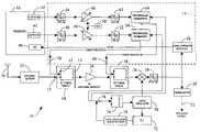
- FIG. 1is a schematic view of a system for generating a tuning voltage utilizing a dual tuning voltage output
- FIG. 2is a block diagram of a technique for controlling a processor utilizing the dual tuning voltage output
- FIG. 3is a schematic view of a system for creating a tuning voltage utilizing a single tuning voltage output
- FIG. 4is a block diagram of a technique for controlling a processor utilizing a single tuning voltage output.
- the system 10includes a processor 12 , a tank circuit (RF tuning tank # 1 ) 14 , and a feedback loop 17 .
- a radio signalis received an through antenna 30 and provided to a matching network 32 that is matched to the impedance of the antenna 30 to optimize power transfer to the tuner circuit.
- the radio signalis provided from the matching network 32 to the tank circuit 14 .
- the tank circuit 14defines a selectivity frequency band based on the inductance and capacitance of the tank circuit 14 .
- the tank circuit 14may include varactors 15 in a parallel electrical configuration with an inductor 13 .
- the capacitance of the varactors 15change based on the tuning voltage supplied to the varactors 15 .
- the tank circuit 14then provides the radio signal to an RF low noise amplifier 34 .
- the low noise amplifier 34provides the radio signal to a second tank circuit (RF tuning tank # 2 ) 16 .
- the second tank circuit 16defines a second selectivity frequency band that further narrows the frequency band in the radio signal.
- the second tuning tank 16provides the radio signal to a mixer 36 , and the mixer 36 combines the radio signal with a local oscillator signal, from a local oscillator circuit 70 , to generate an intermediate frequency (IF) signal.
- IFintermediate frequency
- the filter 38provides the intermediate frequency signal to both the signal strength detector 18 and the demodulator 20 .
- the signal strength detector 18generates an analog signal that corresponds to the signal strength of the radio signal.
- the signal strength detector 18provides the analog signal to an analog to digital (A/D) converter 40 of the processor 12 .
- the demodulator 20converts the intermediate frequency signal into an analog audio output signal 22 .
- the processor 12analyzes analog signal utilizing the internal analog to digital converter 40 .
- the system 10utilizes analog tuning voltages for adjustment of the system's tank circuits 14 , 16 .
- Conventional facilities in the processor 12may be used for generating the tuning voltage.
- a pulse width modulated control signalmay be generated by the processor 12 and used to tune the tank circuits 14 , 16 .
- the feedback loop 17is accomplished by measuring the radio signal strength through the processor's internal analog to digital converter 40 . The measurement is compared with calibration values that are determined for each tank circuit 14 , 16 during the manufacturing process. The processor 12 varies the duty cycle of the control signal to fine tune the desired voltage needed for each particular tank circuit 14 , 16 . Once the desired voltage is reached, the duty cycle of the pulse width modulated control signal may remain constant until a need for readjusting the voltage arises.
- the processor 12controls a first output (output # 1 ) 42 and a second output (output # 2 ) 44 to generate the tuning voltages.
- the processor 12utilizes the analog signal from the signal strength detector 18 , the processor 12 inherently controls the tuning voltages based on the radio signal strength.
- the first output 42provides a first control signal to a low pass filter (L.P.F. # 1 ) 46 .
- the first output 42is a pulse width modulator and the first control signal is a pulse width modulated control signal, where the duty cycle of the control signal is manipulated to adjust the tuning voltages.
- the low pass filter 46removes high frequency components from the tuning voltage.
- the first control signalis provided from the low pass filter 46 to an amplifier 48 that increases the amplitude of the first control signal according to a reference voltage (VCC) 50 .
- VCCreference voltage
- the first tuning voltageis then provided to another low pass filter (L.P.F. # 2 ) 52 .
- L.P.F. # 2low pass filter
- the first control signalis provided to a proportional combiner (proportional combiner # 1 ) 54 .
- the proportional combiner 54combines the first control signal with a local oscillator tuning voltage signal from a local oscillator tuning voltage circuit 78 . The combination results in a first tuning voltage signal that is provided through a load 56 to the first tank circuit 14 .
- the second output (output # 2 ) 44may also be a pulse width modulator.
- the second output 44provides a second control signal to a low pass filter (L.P.F. # 3 ) 58 .
- the second control signalis provided from the low pass filter 58 to an amplifier 60 .
- the amplifier 60increases the amplitude of the second control signal based on the reference voltage 50 and provides the second control signal to the low pass filter (L.P.F. # 4 ) 62 .
- the second control signalis provided from the low pass filter 62 to the proportional combiner (proportional combiner # 2 ) 64 where it is combined with the local oscillator tuning voltage signal from the local oscillator tuning voltage circuit 78 .
- a second tuning voltage signal, resulting from the combination,is provided from the proportional combiner 64 through a load 68 to the second tuning tank 16 .
- the first and second tank circuit 14 and 16function cooperatively to provide a more precise selectivity band for the tuning circuit.
- any number of tank circuitsmay be provided in series in a similar manner to further narrow the bandwidth to increase selectivity.
- the mixer 36is in communication with the local oscillator circuit 70 .
- a local oscillator signalis provided from the local oscillator circuit 70 to the mixer 36 to mix the local oscillator signal with a radio signal from the second tuning tank 16 .
- a signal from the local oscillator circuit 70is provided to the phase lock loop (PLL) 72 .
- the phase lock loop 72provides an error signal to the local oscillator tuning voltage circuit 78 , which generates the local oscillator tuning voltage signal that is provided to the first and second proportional combiners 54 and 64 .
- the local oscillation tuning voltage signalis provided to a third tank circuit 76 through a load 74 .
- the third tank circuit 76is configured to select the frequency of the oscillation signal. Accordingly, the output of the third tank circuit 76 is provided to the local oscillator circuit 70 .
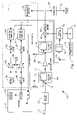
- a method for generating tuning voltage signalsstarts in block 100 upon retuning of the system.
- the processorreads the analog to digital converter to generate a measurement value indicative of the signal strength voltage.
- the measurementis provided to both blocks 104 and 106 .
- the processordetermines if the measured value is equal to the desired voltage for a first tank circuit at the given frequency. Accordingly, the processor may include a memory having a lookup table that is indicative of the optimal tuning voltage for the tank circuit at the given frequency. If the measured value equals the desired voltage for the first tank circuit, the method follows line 108 and the value is saved to memory block 110 . In block 112 , the processor uses the fixed value that was saved in block 110 to generate a controlled duty cycle tuning voltage signal that is provided to the first tank circuit 14 . In block 111 , the method then ends for the first tuning circuit until retuning is required.
- the logicfollows line 116 to block 118 .
- the processor 12calculates a change in the control duty cycle signal, which is calculated to reduce the error between the measured value and the desired voltage for the first tank circuit 14 at the given frequency.
- the information from block 118is provided to block 114 where the control duty cycle tuning voltage signal is provided to the first tank circuit 14 .
- the processor 12reads analog to digital converter and the feedback loop continues.
- the processordetermines if the measured value is equal to the desired voltage for a second tank circuit 16 at the given frequency. Accordingly, the processor may include a memory having a lookup table that is indicative of the optimal tuning voltage for the second tank circuit 16 at the given frequency. If the measured value equals the desired voltage for the second tank circuit 16 , the method follows line 122 and the value is saved to memory in block 124 . In block 126 , the processor 12 uses the fixed value that was saved in block 124 to generate a controlled-duty cycle tuning voltage signal that is provided to the second tank circuit 16 . In block 111 , the method for the second tank circuit then ends until retuning is required.
- the logicfollows line 128 to block 130 .
- the processor 12calculates a change in the control duty cycle signal calculated to reduce the error between the measured value and the desired voltage for the second tank circuit 16 at the given frequency.
- the information from block 130is provided to block 127 where the control duty cycle tuning voltage signal is provided to the second tank circuit 16 .
- the processor 12again reads the analog to digital converter in box 102 and the feedback loop continues.
- a system 210 utilizing a single output techniqueis provided.
- a radio transmission signalis received through antenna 230 and provided to a matching network 232 that is matched to the impedance of the antenna 230 to optimize power transfer to the tuner circuit.
- the radio signalis provided from the matching network 232 to a first tank circuit (RF tuning tank # 1 ) 214 .
- the tank circuit 214defines a selectivity frequency band based on the inductance and capacitance of the tank circuit 214 .
- the tank circuit 214then provides the radio signal to a (RF) low noise amplifier 234 .
- the low noise amplifier 234provides the radio signal to a second tank circuit (RF tuning tank # 2 ) 216 , which defines a second selectivity frequency band that further narrows the frequency band in the radio signal.
- the second tuning tank 216provides the radio signal to a mixer 236 .
- the mixer 236combines the radio signal with a local oscillator signal, from a local oscillator circuit 270 , to generate an intermediate frequency signal.
- the intermediate frequency signalis provided to a filter 238 .
- the filter 238provides the intermediate frequency signal to both the signal strength detector 218 and the demodulator 220 .
- the signal strength detector 218generates an analog signal that corresponds to the signal strength of the radio signal.
- the signal strength detector 218provides the analog signal to an analog to digital converter 240 in the processor 212 .
- the demodulator 220converts the intermediate frequency signal into an analog audio output signal 222 .
- the processor 212analyzes analog signal utilizing the internal analog to digital (A/D) converter 240 . Based on the analysis, the processor 212 controls an output 242 to generate a tuning voltage. Accordingly, the processor 212 inherently controls the tuning voltage based on the radio signal strength from the signal strength detector 218 .
- the output 242provides a control signal to a low pass filter (L.P.F. # 1 ) 246 .
- the output 242is a pulse width modulator and the control signal is a pulse width modulated control signal, where the duty cycle of the control signal is manipulated to adjust the tuning voltage.
- the low pass filter 246removes high frequency components from the tuning voltage.
- the control signalis provided from the low pass filter 246 to an amplifier 248 that increases the amplitude of the control signal according to a reference voltage (VCC) 250 .
- VCCreference voltage
- the tuning voltageis then provided to another low pass filter (L.P.F. # 2 ) 252 .
- the control signalis provided from the low pass filter 252 to a proportional combiner 254 , and the proportional combiner 254 combines the control signal with a local oscillator tuning voltage signal from a local oscillator tuning voltage circuit 278 .
- the combinationresults in a tuning voltage signal that is provided through a load 256 to the first tank circuit 214 .
- the mixer 236is in communication with a local oscillator circuit 270 .
- the local oscillator signalis provided from the local oscillator circuit 270 to the mixer 236 to combine the local oscillator signal with a radio signal from the second tuning tank 216 .
- a signal from the local oscillator circuit 270is also provided to a phase lock loop (PLL) 272 .
- the phase lock loop 272provides an error signal to the local oscillator tuning voltage circuit 278 .
- the local oscillator tuning voltage circuit 278generates the local oscillator tuning voltage signal that is provided to the proportional combiner 254 and the second tuning tank 216 .
- the local oscillator tuning voltage signalis provided to a third tank circuit 276 through a load 274 .
- the third tank circuit 276is configured to select the frequency of the oscillation signal. Accordingly, the output of the third tank circuit 276 is provided to the local oscillator circuit 270 .
- a method for generating tuning voltage signals with a signalstarts in block 300 upon retuning of the system.
- the processor 212reads the analog to digital converter 240 to generate a measurement value indicative of the signal strength voltage.
- the measurementis provided to block 304 .
- the processor 212determines if the measured value is equal to the desired voltage for a first tank circuit 214 at the given frequency. Accordingly, the processor 212 may include a memory having a lookup table that is indicative of the optimal tuning voltage for the tank circuit 214 at the given frequency. If the measured value equals the desired voltage for the first tank circuit 214 , the method follows line 308 and the value is saved to memory in block 310 . In block 312 , the processor 212 uses the fixed value that was saved in block 310 to generate a controlled duty cycle tuning voltage signal that is provided to the first tank circuit 214 . The method then ends in block 311 until retuning is required.
- the logicfollows line 316 to block 318 .
- the processor 212calculates a change in the control duty cycle signal calculated to reduce the error between the measured value and the desired voltage for the first tank circuit 214 at the given frequency.
- the information from block 318is provided to block 314 where the control duty cycle tuning voltage signal is provided to the first tank circuit 214 .
- the processor 212reads analog to digital converter 240 and the feedback loop 217 continues.
Landscapes
- Engineering & Computer Science (AREA)
- Computer Networks & Wireless Communication (AREA)
- Signal Processing (AREA)
- Computer Hardware Design (AREA)
- Microelectronics & Electronic Packaging (AREA)
- Superheterodyne Receivers (AREA)
- Channel Selection Circuits, Automatic Tuning Circuits (AREA)
Abstract
Description
Claims (17)
Priority Applications (2)
| Application Number | Priority Date | Filing Date | Title |
|---|---|---|---|
| US11/540,269US7660566B2 (en) | 2006-09-29 | 2006-09-29 | System for creating a programmable tuning voltage |
| DE102007047263.5ADE102007047263B4 (en) | 2006-09-29 | 2007-09-25 | System for generating a programmable tuning voltage |
Applications Claiming Priority (1)
| Application Number | Priority Date | Filing Date | Title |
|---|---|---|---|
| US11/540,269US7660566B2 (en) | 2006-09-29 | 2006-09-29 | System for creating a programmable tuning voltage |
Publications (2)
| Publication Number | Publication Date |
|---|---|
| US20080081589A1 US20080081589A1 (en) | 2008-04-03 |
| US7660566B2true US7660566B2 (en) | 2010-02-09 |
Family
ID=39198594
Family Applications (1)
| Application Number | Title | Priority Date | Filing Date |
|---|---|---|---|
| US11/540,269Expired - Fee RelatedUS7660566B2 (en) | 2006-09-29 | 2006-09-29 | System for creating a programmable tuning voltage |
Country Status (2)
| Country | Link |
|---|---|
| US (1) | US7660566B2 (en) |
| DE (1) | DE102007047263B4 (en) |
Cited By (6)
| Publication number | Priority date | Publication date | Assignee | Title |
|---|---|---|---|---|
| US20070052482A1 (en)* | 2005-06-30 | 2007-03-08 | Kasha Dan B | Low noise amplifier for a radio receiver |
| US20090156147A1 (en)* | 2007-12-12 | 2009-06-18 | Ahmadreza Rofougaran | Method and system for on-demand receiver supply voltage and current |
| US20110159828A1 (en)* | 2009-12-29 | 2011-06-30 | Kasha Dan B | Configurable Radio Front End |
| US8463215B2 (en) | 2009-12-29 | 2013-06-11 | Silicon Laboratories Inc. | Integrating components in a radio tuner integrated circuit (IC) for a tracking filter |
| US8818309B2 (en) | 2011-03-28 | 2014-08-26 | Silicon Laboratories Inc. | Providing multiple inductors for a radio tuner |
| US9264080B2 (en) | 2014-01-31 | 2016-02-16 | Silicon Laboratories Inc. | Reducing second order distortion in an amplifier |
Families Citing this family (2)
| Publication number | Priority date | Publication date | Assignee | Title |
|---|---|---|---|---|
| US8494474B1 (en)* | 2010-11-29 | 2013-07-23 | The United States Of America As Represented By The Secretary Of The Navy | Dual band diode mixer for RF data receiver |
| US9960748B2 (en)* | 2015-07-07 | 2018-05-01 | Provenance Asset Group Llc | RF filter suppression tuning based on transmit power |
Citations (27)
| Publication number | Priority date | Publication date | Assignee | Title |
|---|---|---|---|---|
| US4011515A (en)* | 1975-05-23 | 1977-03-08 | General Electric Company | Tunable scanning radio receiver |
| US4061981A (en) | 1976-08-18 | 1977-12-06 | General Motors Corporation | Voltage variable capacitor tuned radio receiver having delayed automatic frequency control at turn-on |
| US4361907A (en) | 1980-08-14 | 1982-11-30 | Rca Corporation | Direct access channel selection apparatus for a digital tuning system |
| US4472685A (en) | 1980-04-25 | 1984-09-18 | Thomson-Brandt | Phase-locked loop frequency demodulator and frequency synthesizer |
| US4590611A (en) | 1983-02-04 | 1986-05-20 | Deutsche Thomson-Brandt Gmbh | Tuner for communications equipment |
| US4641101A (en) | 1984-10-25 | 1987-02-03 | Ifr, Inc. | Wideband, microwave regenerative divider with varactor tuning |
| US4685150A (en) | 1983-03-11 | 1987-08-04 | Deutsche Thomson-Brandt Gmbh | Tuning of a resonant circuit in a communications receiver |
| US5175884A (en) | 1990-06-01 | 1992-12-29 | Motorola, Inc. | Voltage controlled oscillator with current control |
| US5179726A (en) | 1989-11-29 | 1993-01-12 | Samsung Electro-Mechanics Co., Ltd. | Automatic tuning method and apparatus of double conversion tuner |
| JPH0583151A (en) | 1991-09-19 | 1993-04-02 | Matsushita Electric Ind Co Ltd | Am radio receiver |
| US5510859A (en)* | 1993-07-27 | 1996-04-23 | Information Resources, Inc. | Tuned signal detector for use with a radio frequency receiver |
| US5625316A (en) | 1994-07-01 | 1997-04-29 | Motorola, Inc. | Tuning circuit for an RC filter |
| US5678211A (en) | 1992-08-28 | 1997-10-14 | Thomson Consumer Electronics, Inc. | Television tuning apparatus |
| US5745844A (en)* | 1996-10-04 | 1998-04-28 | Motorola, Inc. | Receiver control in a communication device by antenna de-tuning in strong signal conditions, and method therefor |
| US5752179A (en) | 1995-08-17 | 1998-05-12 | Zenith Electronics Corporation | Selective RF circuit with varactor tuned and switched bandpass filters |
| US5822687A (en) | 1991-11-04 | 1998-10-13 | Motorola, Inc. | Method and apparatus for automatic tuning calibration of electrically tuned filters |
| US6021322A (en) | 1996-12-10 | 2000-02-01 | Toko, Inc. | AM radio receiver |
| US6023198A (en) | 1998-06-08 | 2000-02-08 | Motorola, Inc. | Self-tuning and temperature compensated voltage controlled oscillator |
| US6496075B2 (en) | 2001-03-14 | 2002-12-17 | Ericsson Inc. | Automatic tuning of VCO |
| US6728651B1 (en) | 2002-03-13 | 2004-04-27 | Ltx Corporation | Methods and apparatuses for digitally tuning a phased-lock loop circuit |
| US20040116091A1 (en) | 2002-12-13 | 2004-06-17 | Mcginn Michael | Tuning signal generator and method thereof |
| US20040127181A1 (en) | 2002-12-30 | 2004-07-01 | Galan Ariel L. | Apparatus and method for a radio frequency (RF) receiver front end pre-selector tuning for improving the reduction in intermodulation distortion (IMD) |
| US20050104765A1 (en) | 2003-11-16 | 2005-05-19 | Brian Bandhauer | Radar frequency hopping |
| US20050134344A1 (en) | 2003-12-22 | 2005-06-23 | Globespan Virata, Inc. | Fast start-up circuit for a prescaler device |
| US6957053B1 (en) | 1999-05-26 | 2005-10-18 | Siemens Ag | Method for selection of a receiver tuning frequency |
| US20060084396A1 (en) | 1998-11-30 | 2006-04-20 | Scott Matthew | Smart tuning AM transmitter |
| US7236741B2 (en)* | 2001-03-16 | 2007-06-26 | Aura Communications Technology, Inc. | Methods and apparatus for tuning in an inductive system |
Family Cites Families (4)
| Publication number | Priority date | Publication date | Assignee | Title |
|---|---|---|---|---|
| GB2173661B (en)* | 1985-03-22 | 1989-06-28 | Victor Company Of Japan | Superheterodyne television tuner |
| DE4011839C2 (en)* | 1990-04-12 | 1999-02-25 | Thomson Brandt Gmbh | Circuit arrangement for the adjustment of HF filter circuits |
| US5280638A (en)* | 1991-09-06 | 1994-01-18 | Ford Motor Company | RF filter self-alignment for multiband radio receiver |
| DE19918057C2 (en)* | 1999-04-21 | 2002-11-07 | Infineon Technologies Ag | Device for adjusting the tuning voltage of tuning resonant circuits |
- 2006
- 2006-09-29USUS11/540,269patent/US7660566B2/ennot_activeExpired - Fee Related
- 2007
- 2007-09-25DEDE102007047263.5Apatent/DE102007047263B4/ennot_activeExpired - Fee Related
Patent Citations (27)
| Publication number | Priority date | Publication date | Assignee | Title |
|---|---|---|---|---|
| US4011515A (en)* | 1975-05-23 | 1977-03-08 | General Electric Company | Tunable scanning radio receiver |
| US4061981A (en) | 1976-08-18 | 1977-12-06 | General Motors Corporation | Voltage variable capacitor tuned radio receiver having delayed automatic frequency control at turn-on |
| US4472685A (en) | 1980-04-25 | 1984-09-18 | Thomson-Brandt | Phase-locked loop frequency demodulator and frequency synthesizer |
| US4361907A (en) | 1980-08-14 | 1982-11-30 | Rca Corporation | Direct access channel selection apparatus for a digital tuning system |
| US4590611A (en) | 1983-02-04 | 1986-05-20 | Deutsche Thomson-Brandt Gmbh | Tuner for communications equipment |
| US4685150A (en) | 1983-03-11 | 1987-08-04 | Deutsche Thomson-Brandt Gmbh | Tuning of a resonant circuit in a communications receiver |
| US4641101A (en) | 1984-10-25 | 1987-02-03 | Ifr, Inc. | Wideband, microwave regenerative divider with varactor tuning |
| US5179726A (en) | 1989-11-29 | 1993-01-12 | Samsung Electro-Mechanics Co., Ltd. | Automatic tuning method and apparatus of double conversion tuner |
| US5175884A (en) | 1990-06-01 | 1992-12-29 | Motorola, Inc. | Voltage controlled oscillator with current control |
| JPH0583151A (en) | 1991-09-19 | 1993-04-02 | Matsushita Electric Ind Co Ltd | Am radio receiver |
| US5822687A (en) | 1991-11-04 | 1998-10-13 | Motorola, Inc. | Method and apparatus for automatic tuning calibration of electrically tuned filters |
| US5678211A (en) | 1992-08-28 | 1997-10-14 | Thomson Consumer Electronics, Inc. | Television tuning apparatus |
| US5510859A (en)* | 1993-07-27 | 1996-04-23 | Information Resources, Inc. | Tuned signal detector for use with a radio frequency receiver |
| US5625316A (en) | 1994-07-01 | 1997-04-29 | Motorola, Inc. | Tuning circuit for an RC filter |
| US5752179A (en) | 1995-08-17 | 1998-05-12 | Zenith Electronics Corporation | Selective RF circuit with varactor tuned and switched bandpass filters |
| US5745844A (en)* | 1996-10-04 | 1998-04-28 | Motorola, Inc. | Receiver control in a communication device by antenna de-tuning in strong signal conditions, and method therefor |
| US6021322A (en) | 1996-12-10 | 2000-02-01 | Toko, Inc. | AM radio receiver |
| US6023198A (en) | 1998-06-08 | 2000-02-08 | Motorola, Inc. | Self-tuning and temperature compensated voltage controlled oscillator |
| US20060084396A1 (en) | 1998-11-30 | 2006-04-20 | Scott Matthew | Smart tuning AM transmitter |
| US6957053B1 (en) | 1999-05-26 | 2005-10-18 | Siemens Ag | Method for selection of a receiver tuning frequency |
| US6496075B2 (en) | 2001-03-14 | 2002-12-17 | Ericsson Inc. | Automatic tuning of VCO |
| US7236741B2 (en)* | 2001-03-16 | 2007-06-26 | Aura Communications Technology, Inc. | Methods and apparatus for tuning in an inductive system |
| US6728651B1 (en) | 2002-03-13 | 2004-04-27 | Ltx Corporation | Methods and apparatuses for digitally tuning a phased-lock loop circuit |
| US20040116091A1 (en) | 2002-12-13 | 2004-06-17 | Mcginn Michael | Tuning signal generator and method thereof |
| US20040127181A1 (en) | 2002-12-30 | 2004-07-01 | Galan Ariel L. | Apparatus and method for a radio frequency (RF) receiver front end pre-selector tuning for improving the reduction in intermodulation distortion (IMD) |
| US20050104765A1 (en) | 2003-11-16 | 2005-05-19 | Brian Bandhauer | Radar frequency hopping |
| US20050134344A1 (en) | 2003-12-22 | 2005-06-23 | Globespan Virata, Inc. | Fast start-up circuit for a prescaler device |
Cited By (11)
| Publication number | Priority date | Publication date | Assignee | Title |
|---|---|---|---|---|
| US20070052482A1 (en)* | 2005-06-30 | 2007-03-08 | Kasha Dan B | Low noise amplifier for a radio receiver |
| US8346198B2 (en) | 2005-06-30 | 2013-01-01 | Silicon Laboratories Inc. | Low noise amplifier for a radio receiver |
| US20090156147A1 (en)* | 2007-12-12 | 2009-06-18 | Ahmadreza Rofougaran | Method and system for on-demand receiver supply voltage and current |
| US8447260B2 (en)* | 2007-12-12 | 2013-05-21 | Broadcom Corporation | Method and system for on-demand receiver supply voltage and current |
| US20110159828A1 (en)* | 2009-12-29 | 2011-06-30 | Kasha Dan B | Configurable Radio Front End |
| US8254862B2 (en)* | 2009-12-29 | 2012-08-28 | Silicon Laboratories Inc. | Configurable radio front end |
| US8463215B2 (en) | 2009-12-29 | 2013-06-11 | Silicon Laboratories Inc. | Integrating components in a radio tuner integrated circuit (IC) for a tracking filter |
| US8750819B2 (en) | 2009-12-29 | 2014-06-10 | Silicon Laboratories Inc. | Integrating components in a radio tuner integrated circuit (IC) for a tracking filter |
| US8818309B2 (en) | 2011-03-28 | 2014-08-26 | Silicon Laboratories Inc. | Providing multiple inductors for a radio tuner |
| US9002306B2 (en) | 2011-03-28 | 2015-04-07 | Silicon Laboratories Inc. | Providing multiple inductors for a radio tuner |
| US9264080B2 (en) | 2014-01-31 | 2016-02-16 | Silicon Laboratories Inc. | Reducing second order distortion in an amplifier |
Also Published As
| Publication number | Publication date |
|---|---|
| US20080081589A1 (en) | 2008-04-03 |
| DE102007047263A1 (en) | 2008-04-24 |
| DE102007047263B4 (en) | 2016-04-07 |
Similar Documents
| Publication | Publication Date | Title |
|---|---|---|
| US7660566B2 (en) | System for creating a programmable tuning voltage | |
| US5428829A (en) | Method and apparatus for tuning and aligning an FM receiver | |
| US7620379B2 (en) | Radio frequency tuner | |
| US6882246B2 (en) | System and method for an electronically tunable frequency filter having constant bandwidth and temperature compensation for center frequency, bandwidth and insertion loss | |
| TWI406496B (en) | Image rejection mixer providing precision image rejection | |
| US10951190B2 (en) | On-chip harmonic filtering for radio frequency (RF) communications | |
| JP2002368642A (en) | Receiver and ic | |
| US20090128240A1 (en) | Oscillator, pll circuit, receiver and transmitter | |
| JP3250785B2 (en) | TV tuner | |
| JPS63242030A (en) | wideband frequency synthesizer receiver | |
| US7756496B2 (en) | Oscillation controlling apparatus, recording medium having program recorded thereon, and channel selecting apparatus | |
| US8150362B2 (en) | Electronically tuned agile integrated bandpass filter | |
| US5301366A (en) | High performance frequency tuning with low cost synthesizer | |
| US20040012454A1 (en) | Wideband VCO resonant circuit method and apparatus | |
| JPS61251313A (en) | Electronic tuning type fm receiver | |
| US7945218B1 (en) | Method and system for tuning quality factor in high-Q, high-frequency filters | |
| US20050221776A1 (en) | Test signal generation circuit, and reception circuit | |
| US6091943A (en) | Combining oscillator with a phase-indexed control circuit for a radio receiver | |
| CN100379271C (en) | High frequency signal receiver | |
| US8369446B2 (en) | Transmitter | |
| CN1726640B (en) | Tunable tracking filter | |
| KR100282193B1 (en) | Stereo signal demodulation circuit and stereo signal demodulation device using the same | |
| US7650123B2 (en) | Receiver and a method of attenuating a disturbance signal by a trap circuit having its resonance frequency adjustable | |
| JP2007096381A (en) | Antenna input unit | |
| JP2000341091A (en) | Input trap circuit and image trap circuit |
Legal Events
| Date | Code | Title | Description |
|---|---|---|---|
| AS | Assignment | Owner name:VISTEON GLOBAL TECHNOLOGIES, INC., MICHIGAN Free format text:ASSIGNMENT OF ASSIGNORS INTEREST;ASSIGNORS:KUO, YAO H.;WHARAM, THOMAS;REEL/FRAME:018381/0696;SIGNING DATES FROM 20060926 TO 20060928 Owner name:VISTEON GLOBAL TECHNOLOGIES, INC.,MICHIGAN Free format text:ASSIGNMENT OF ASSIGNORS INTEREST;ASSIGNORS:KUO, YAO H.;WHARAM, THOMAS;SIGNING DATES FROM 20060926 TO 20060928;REEL/FRAME:018381/0696 | |
| AS | Assignment | Owner name:WILMINGTON TRUST FSB, AS ADMINISTRATIVE AGENT, MIN Free format text:GRANT OF SECURITY INTEREST IN PATENT RIGHTS;ASSIGNOR:VISTEON GLOBAL TECHNOLOGIES, INC.;REEL/FRAME:022619/0938 Effective date:20090430 Owner name:WILMINGTON TRUST FSB, AS ADMINISTRATIVE AGENT,MINN Free format text:GRANT OF SECURITY INTEREST IN PATENT RIGHTS;ASSIGNOR:VISTEON GLOBAL TECHNOLOGIES, INC.;REEL/FRAME:022619/0938 Effective date:20090430 | |
| AS | Assignment | Owner name:VISTEON GLOBAL TECHNOLOGIES, INC., MICHIGAN Free format text:RELEASE BY SECURED PARTY AGAINST SECURITY INTEREST IN PATENTS RECORDED AT REEL 022619 FRAME 0938;ASSIGNOR:WILMINGTON TRUST FSB;REEL/FRAME:025095/0466 Effective date:20101001 | |
| AS | Assignment | Owner name:MORGAN STANLEY SENIOR FUNDING, INC., AS AGENT, NEW Free format text:SECURITY AGREEMENT (REVOLVER);ASSIGNORS:VISTEON CORPORATION;VC AVIATION SERVICES, LLC;VISTEON ELECTRONICS CORPORATION;AND OTHERS;REEL/FRAME:025238/0298 Effective date:20101001 Owner name:MORGAN STANLEY SENIOR FUNDING, INC., AS AGENT, NEW Free format text:SECURITY AGREEMENT;ASSIGNORS:VISTEON CORPORATION;VC AVIATION SERVICES, LLC;VISTEON ELECTRONICS CORPORATION;AND OTHERS;REEL/FRAME:025241/0317 Effective date:20101007 | |
| AS | Assignment | Owner name:VISTEON CORPORATION, MICHIGAN Free format text:RELEASE BY SECURED PARTY AGAINST SECURITY INTEREST IN PATENTS ON REEL 025241 FRAME 0317;ASSIGNOR:MORGAN STANLEY SENIOR FUNDING, INC.;REEL/FRAME:026178/0412 Effective date:20110406 Owner name:VISTEON INTERNATIONAL HOLDINGS, INC., MICHIGAN Free format text:RELEASE BY SECURED PARTY AGAINST SECURITY INTEREST IN PATENTS ON REEL 025241 FRAME 0317;ASSIGNOR:MORGAN STANLEY SENIOR FUNDING, INC.;REEL/FRAME:026178/0412 Effective date:20110406 Owner name:VISTEON SYSTEMS, LLC, MICHIGAN Free format text:RELEASE BY SECURED PARTY AGAINST SECURITY INTEREST IN PATENTS ON REEL 025241 FRAME 0317;ASSIGNOR:MORGAN STANLEY SENIOR FUNDING, INC.;REEL/FRAME:026178/0412 Effective date:20110406 Owner name:VISTEON ELECTRONICS CORPORATION, MICHIGAN Free format text:RELEASE BY SECURED PARTY AGAINST SECURITY INTEREST IN PATENTS ON REEL 025241 FRAME 0317;ASSIGNOR:MORGAN STANLEY SENIOR FUNDING, INC.;REEL/FRAME:026178/0412 Effective date:20110406 Owner name:VISTEON EUROPEAN HOLDING, INC., MICHIGAN Free format text:RELEASE BY SECURED PARTY AGAINST SECURITY INTEREST IN PATENTS ON REEL 025241 FRAME 0317;ASSIGNOR:MORGAN STANLEY SENIOR FUNDING, INC.;REEL/FRAME:026178/0412 Effective date:20110406 Owner name:VISTEON GLOBAL TREASURY, INC., MICHIGAN Free format text:RELEASE BY SECURED PARTY AGAINST SECURITY INTEREST IN PATENTS ON REEL 025241 FRAME 0317;ASSIGNOR:MORGAN STANLEY SENIOR FUNDING, INC.;REEL/FRAME:026178/0412 Effective date:20110406 Owner name:VISTEON GLOBAL TECHNOLOGIES, INC., MICHIGAN Free format text:RELEASE BY SECURED PARTY AGAINST SECURITY INTEREST IN PATENTS ON REEL 025241 FRAME 0317;ASSIGNOR:MORGAN STANLEY SENIOR FUNDING, INC.;REEL/FRAME:026178/0412 Effective date:20110406 Owner name:VISTEON INTERNATIONAL BUSINESS DEVELOPMENT, INC., Free format text:RELEASE BY SECURED PARTY AGAINST SECURITY INTEREST IN PATENTS ON REEL 025241 FRAME 0317;ASSIGNOR:MORGAN STANLEY SENIOR FUNDING, INC.;REEL/FRAME:026178/0412 Effective date:20110406 Owner name:VC AVIATION SERVICES, LLC, MICHIGAN Free format text:RELEASE BY SECURED PARTY AGAINST SECURITY INTEREST IN PATENTS ON REEL 025241 FRAME 0317;ASSIGNOR:MORGAN STANLEY SENIOR FUNDING, INC.;REEL/FRAME:026178/0412 Effective date:20110406 | |
| REMI | Maintenance fee reminder mailed | ||
| LAPS | Lapse for failure to pay maintenance fees | ||
| STCH | Information on status: patent discontinuation | Free format text:PATENT EXPIRED DUE TO NONPAYMENT OF MAINTENANCE FEES UNDER 37 CFR 1.362 | |
| FP | Lapsed due to failure to pay maintenance fee | Effective date:20140209 | |
| AS | Assignment | Owner name:VISTEON CORPORATION, MICHIGAN Free format text:RELEASE OF SECURITY INTEREST IN INTELLECTUAL PROPERTY;ASSIGNOR:MORGAN STANLEY SENIOR FUNDING, INC.;REEL/FRAME:033107/0717 Effective date:20140409 Owner name:VC AVIATION SERVICES, LLC, MICHIGAN Free format text:RELEASE OF SECURITY INTEREST IN INTELLECTUAL PROPERTY;ASSIGNOR:MORGAN STANLEY SENIOR FUNDING, INC.;REEL/FRAME:033107/0717 Effective date:20140409 Owner name:VISTEON SYSTEMS, LLC, MICHIGAN Free format text:RELEASE OF SECURITY INTEREST IN INTELLECTUAL PROPERTY;ASSIGNOR:MORGAN STANLEY SENIOR FUNDING, INC.;REEL/FRAME:033107/0717 Effective date:20140409 Owner name:VISTEON GLOBAL TECHNOLOGIES, INC., MICHIGAN Free format text:RELEASE OF SECURITY INTEREST IN INTELLECTUAL PROPERTY;ASSIGNOR:MORGAN STANLEY SENIOR FUNDING, INC.;REEL/FRAME:033107/0717 Effective date:20140409 Owner name:VISTEON EUROPEAN HOLDINGS, INC., MICHIGAN Free format text:RELEASE OF SECURITY INTEREST IN INTELLECTUAL PROPERTY;ASSIGNOR:MORGAN STANLEY SENIOR FUNDING, INC.;REEL/FRAME:033107/0717 Effective date:20140409 Owner name:VISTEON INTERNATIONAL HOLDINGS, INC., MICHIGAN Free format text:RELEASE OF SECURITY INTEREST IN INTELLECTUAL PROPERTY;ASSIGNOR:MORGAN STANLEY SENIOR FUNDING, INC.;REEL/FRAME:033107/0717 Effective date:20140409 Owner name:VISTEON ELECTRONICS CORPORATION, MICHIGAN Free format text:RELEASE OF SECURITY INTEREST IN INTELLECTUAL PROPERTY;ASSIGNOR:MORGAN STANLEY SENIOR FUNDING, INC.;REEL/FRAME:033107/0717 Effective date:20140409 Owner name:VISTEON INTERNATIONAL BUSINESS DEVELOPMENT, INC., Free format text:RELEASE OF SECURITY INTEREST IN INTELLECTUAL PROPERTY;ASSIGNOR:MORGAN STANLEY SENIOR FUNDING, INC.;REEL/FRAME:033107/0717 Effective date:20140409 Owner name:VISTEON GLOBAL TREASURY, INC., MICHIGAN Free format text:RELEASE OF SECURITY INTEREST IN INTELLECTUAL PROPERTY;ASSIGNOR:MORGAN STANLEY SENIOR FUNDING, INC.;REEL/FRAME:033107/0717 Effective date:20140409 |