US7659622B2 - Trace design to minimize electromigration damage to solder bumps - Google Patents
Trace design to minimize electromigration damage to solder bumpsDownload PDFInfo
- Publication number
- US7659622B2 US7659622B2US11/779,833US77983307AUS7659622B2US 7659622 B2US7659622 B2US 7659622B2US 77983307 AUS77983307 AUS 77983307AUS 7659622 B2US7659622 B2US 7659622B2
- Authority
- US
- United States
- Prior art keywords
- pad
- trace
- sub
- traces
- current
- Prior art date
- Legal status (The legal status is an assumption and is not a legal conclusion. Google has not performed a legal analysis and makes no representation as to the accuracy of the status listed.)
- Expired - Fee Related
Links
- 229910000679solderInorganic materials0.000titleclaimsdescription18
- 238000000034methodMethods0.000claimsabstractdescription19
- 239000002184metalSubstances0.000claimsdescription18
- 229910052751metalInorganic materials0.000claimsdescription18
- 230000008878couplingEffects0.000claimsdescription2
- 238000010168coupling processMethods0.000claimsdescription2
- 238000005859coupling reactionMethods0.000claimsdescription2
- 239000010410layerSubstances0.000claims1
- 239000002356single layerSubstances0.000claims1
- 238000009826distributionMethods0.000abstractdescription9
- 239000000758substrateSubstances0.000description14
- 239000000463materialSubstances0.000description11
- 230000008901benefitEffects0.000description6
- 230000000694effectsEffects0.000description6
- 238000004364calculation methodMethods0.000description4
- 239000004020conductorSubstances0.000description4
- 238000002161passivationMethods0.000description4
- 230000008569processEffects0.000description4
- 230000008859changeEffects0.000description3
- 229920000642polymerPolymers0.000description3
- RYGMFSIKBFXOCR-UHFFFAOYSA-NCopperChemical compound[Cu]RYGMFSIKBFXOCR-UHFFFAOYSA-N0.000description2
- 150000001875compoundsChemical class0.000description2
- 229910052802copperInorganic materials0.000description2
- 239000010949copperSubstances0.000description2
- 230000001419dependent effectEffects0.000description2
- 238000004806packaging method and processMethods0.000description2
- -1PbSnChemical class0.000description1
- 229910020658PbSnInorganic materials0.000description1
- 101150071746Pbsn geneProteins0.000description1
- 238000007792additionMethods0.000description1
- 230000002411adverseEffects0.000description1
- 238000004458analytical methodMethods0.000description1
- 238000000429assemblyMethods0.000description1
- 230000000712assemblyEffects0.000description1
- 230000015572biosynthetic processEffects0.000description1
- 238000000151depositionMethods0.000description1
- 238000009713electroplatingMethods0.000description1
- 230000005496eutecticsEffects0.000description1
- 230000008020evaporationEffects0.000description1
- 238000001704evaporationMethods0.000description1
- PCHJSUWPFVWCPO-UHFFFAOYSA-NgoldChemical compound[Au]PCHJSUWPFVWCPO-UHFFFAOYSA-N0.000description1
- 229910052737goldInorganic materials0.000description1
- 239000010931goldSubstances0.000description1
- 229910052745leadInorganic materials0.000description1
- LQBJWKCYZGMFEV-UHFFFAOYSA-Nlead tinChemical compound[Sn].[Pb]LQBJWKCYZGMFEV-UHFFFAOYSA-N0.000description1
- 238000004519manufacturing processMethods0.000description1
- 238000001465metallisationMethods0.000description1
- 230000004048modificationEffects0.000description1
- 238000012986modificationMethods0.000description1
- 150000004767nitridesChemical class0.000description1
- 238000012536packaging technologyMethods0.000description1
- 238000007747platingMethods0.000description1
- 230000002028prematureEffects0.000description1
- 230000009467reductionEffects0.000description1
- 238000007650screen-printingMethods0.000description1
- 239000004065semiconductorSubstances0.000description1
- 230000035945sensitivityEffects0.000description1
- 239000007787solidSubstances0.000description1
- 238000004544sputter depositionMethods0.000description1
- 238000006467substitution reactionMethods0.000description1
- 238000009827uniform distributionMethods0.000description1
- 238000011144upstream manufacturingMethods0.000description1
Images


Classifications
- H—ELECTRICITY
- H01—ELECTRIC ELEMENTS
- H01L—SEMICONDUCTOR DEVICES NOT COVERED BY CLASS H10
- H01L24/00—Arrangements for connecting or disconnecting semiconductor or solid-state bodies; Methods or apparatus related thereto
- H01L24/01—Means for bonding being attached to, or being formed on, the surface to be connected, e.g. chip-to-package, die-attach, "first-level" interconnects; Manufacturing methods related thereto
- H01L24/10—Bump connectors ; Manufacturing methods related thereto
- H—ELECTRICITY
- H01—ELECTRIC ELEMENTS
- H01L—SEMICONDUCTOR DEVICES NOT COVERED BY CLASS H10
- H01L23/00—Details of semiconductor or other solid state devices
- H01L23/58—Structural electrical arrangements for semiconductor devices not otherwise provided for, e.g. in combination with batteries
- H01L23/64—Impedance arrangements
- H01L23/66—High-frequency adaptations
- H—ELECTRICITY
- H01—ELECTRIC ELEMENTS
- H01L—SEMICONDUCTOR DEVICES NOT COVERED BY CLASS H10
- H01L24/00—Arrangements for connecting or disconnecting semiconductor or solid-state bodies; Methods or apparatus related thereto
- H01L24/01—Means for bonding being attached to, or being formed on, the surface to be connected, e.g. chip-to-package, die-attach, "first-level" interconnects; Manufacturing methods related thereto
- H01L24/10—Bump connectors ; Manufacturing methods related thereto
- H01L24/12—Structure, shape, material or disposition of the bump connectors prior to the connecting process
- H01L24/13—Structure, shape, material or disposition of the bump connectors prior to the connecting process of an individual bump connector
- H—ELECTRICITY
- H01—ELECTRIC ELEMENTS
- H01L—SEMICONDUCTOR DEVICES NOT COVERED BY CLASS H10
- H01L2224/00—Indexing scheme for arrangements for connecting or disconnecting semiconductor or solid-state bodies and methods related thereto as covered by H01L24/00
- H01L2224/01—Means for bonding being attached to, or being formed on, the surface to be connected, e.g. chip-to-package, die-attach, "first-level" interconnects; Manufacturing methods related thereto
- H01L2224/10—Bump connectors; Manufacturing methods related thereto
- H01L2224/12—Structure, shape, material or disposition of the bump connectors prior to the connecting process
- H01L2224/13—Structure, shape, material or disposition of the bump connectors prior to the connecting process of an individual bump connector
- H01L2224/13001—Core members of the bump connector
- H01L2224/13099—Material
- H—ELECTRICITY
- H01—ELECTRIC ELEMENTS
- H01L—SEMICONDUCTOR DEVICES NOT COVERED BY CLASS H10
- H01L2224/00—Indexing scheme for arrangements for connecting or disconnecting semiconductor or solid-state bodies and methods related thereto as covered by H01L24/00
- H01L2224/01—Means for bonding being attached to, or being formed on, the surface to be connected, e.g. chip-to-package, die-attach, "first-level" interconnects; Manufacturing methods related thereto
- H01L2224/10—Bump connectors; Manufacturing methods related thereto
- H01L2224/15—Structure, shape, material or disposition of the bump connectors after the connecting process
- H01L2224/16—Structure, shape, material or disposition of the bump connectors after the connecting process of an individual bump connector
- H—ELECTRICITY
- H01—ELECTRIC ELEMENTS
- H01L—SEMICONDUCTOR DEVICES NOT COVERED BY CLASS H10
- H01L2924/00—Indexing scheme for arrangements or methods for connecting or disconnecting semiconductor or solid-state bodies as covered by H01L24/00
- H01L2924/01—Chemical elements
- H01L2924/01023—Vanadium [V]
- H—ELECTRICITY
- H01—ELECTRIC ELEMENTS
- H01L—SEMICONDUCTOR DEVICES NOT COVERED BY CLASS H10
- H01L2924/00—Indexing scheme for arrangements or methods for connecting or disconnecting semiconductor or solid-state bodies as covered by H01L24/00
- H01L2924/01—Chemical elements
- H01L2924/01025—Manganese [Mn]
- H—ELECTRICITY
- H01—ELECTRIC ELEMENTS
- H01L—SEMICONDUCTOR DEVICES NOT COVERED BY CLASS H10
- H01L2924/00—Indexing scheme for arrangements or methods for connecting or disconnecting semiconductor or solid-state bodies as covered by H01L24/00
- H01L2924/01—Chemical elements
- H01L2924/01029—Copper [Cu]
- H—ELECTRICITY
- H01—ELECTRIC ELEMENTS
- H01L—SEMICONDUCTOR DEVICES NOT COVERED BY CLASS H10
- H01L2924/00—Indexing scheme for arrangements or methods for connecting or disconnecting semiconductor or solid-state bodies as covered by H01L24/00
- H01L2924/01—Chemical elements
- H01L2924/01033—Arsenic [As]
- H—ELECTRICITY
- H01—ELECTRIC ELEMENTS
- H01L—SEMICONDUCTOR DEVICES NOT COVERED BY CLASS H10
- H01L2924/00—Indexing scheme for arrangements or methods for connecting or disconnecting semiconductor or solid-state bodies as covered by H01L24/00
- H01L2924/01—Chemical elements
- H01L2924/01074—Tungsten [W]
- H—ELECTRICITY
- H01—ELECTRIC ELEMENTS
- H01L—SEMICONDUCTOR DEVICES NOT COVERED BY CLASS H10
- H01L2924/00—Indexing scheme for arrangements or methods for connecting or disconnecting semiconductor or solid-state bodies as covered by H01L24/00
- H01L2924/01—Chemical elements
- H01L2924/01077—Iridium [Ir]
- H—ELECTRICITY
- H01—ELECTRIC ELEMENTS
- H01L—SEMICONDUCTOR DEVICES NOT COVERED BY CLASS H10
- H01L2924/00—Indexing scheme for arrangements or methods for connecting or disconnecting semiconductor or solid-state bodies as covered by H01L24/00
- H01L2924/01—Chemical elements
- H01L2924/01078—Platinum [Pt]
- H—ELECTRICITY
- H01—ELECTRIC ELEMENTS
- H01L—SEMICONDUCTOR DEVICES NOT COVERED BY CLASS H10
- H01L2924/00—Indexing scheme for arrangements or methods for connecting or disconnecting semiconductor or solid-state bodies as covered by H01L24/00
- H01L2924/01—Chemical elements
- H01L2924/01079—Gold [Au]
- H—ELECTRICITY
- H01—ELECTRIC ELEMENTS
- H01L—SEMICONDUCTOR DEVICES NOT COVERED BY CLASS H10
- H01L2924/00—Indexing scheme for arrangements or methods for connecting or disconnecting semiconductor or solid-state bodies as covered by H01L24/00
- H01L2924/01—Chemical elements
- H01L2924/01082—Lead [Pb]
- H—ELECTRICITY
- H01—ELECTRIC ELEMENTS
- H01L—SEMICONDUCTOR DEVICES NOT COVERED BY CLASS H10
- H01L2924/00—Indexing scheme for arrangements or methods for connecting or disconnecting semiconductor or solid-state bodies as covered by H01L24/00
- H01L2924/013—Alloys
- H01L2924/0132—Binary Alloys
- H01L2924/01322—Eutectic Alloys, i.e. obtained by a liquid transforming into two solid phases
- H—ELECTRICITY
- H01—ELECTRIC ELEMENTS
- H01L—SEMICONDUCTOR DEVICES NOT COVERED BY CLASS H10
- H01L2924/00—Indexing scheme for arrangements or methods for connecting or disconnecting semiconductor or solid-state bodies as covered by H01L24/00
- H01L2924/013—Alloys
- H01L2924/014—Solder alloys
- H—ELECTRICITY
- H01—ELECTRIC ELEMENTS
- H01L—SEMICONDUCTOR DEVICES NOT COVERED BY CLASS H10
- H01L2924/00—Indexing scheme for arrangements or methods for connecting or disconnecting semiconductor or solid-state bodies as covered by H01L24/00
- H01L2924/10—Details of semiconductor or other solid state devices to be connected
- H01L2924/11—Device type
- H01L2924/14—Integrated circuits
- H—ELECTRICITY
- H01—ELECTRIC ELEMENTS
- H01L—SEMICONDUCTOR DEVICES NOT COVERED BY CLASS H10
- H01L2924/00—Indexing scheme for arrangements or methods for connecting or disconnecting semiconductor or solid-state bodies as covered by H01L24/00
- H01L2924/30—Technical effects
- H01L2924/301—Electrical effects
- H01L2924/3011—Impedance
Definitions
- the present inventionrelates generally to flip chip packaging technologies for integrated circuits more particularly to a methodology and trace design for minimizing electromigration damage to solder bumps in a ball grid array or flip-chip package.
- Electromigrationis the movement of material within a conductor that is caused by the flow of electrical current. Electromigration can cause the complete depletion of material within a conductor leading to the loss of continuity. The effect is more apparent at interconnect junctions, for example, in a solder bump connecting a flip-chip die and substrate, and is dependent on the current density (higher being worse than lower), the material (some materials resisting the effects of electromigration more than others), and the geometry of the structure.
- Electromigrationis a problem commonly seen in high-current-flow bumps of flip-chip assemblies, so named because during formation, the die pads are formed on the top layer of the integrated circuit die, bumps are added, and the die is then “flipped” over and connected directly to the chip substrate via the bumps. More specifically, and with reference to FIGS. 1 and 2 , circuit components are formed on a semiconductor wafer using standard fabrication techniques, with local interconnect layers (formed of interleaved metal and dielectric layers) situated closer to the functional circuitry and global interconnect layers formed further up the sequence of layers. Die pads 22 are formed in the uppermost metal layer. Bumps are then added, and the wafer is diced into individual integrated circuit die 14 for packaging. An individual die 14 is then “flipped” over and attached directly to a substrate 12 or board through the bumps 16 , as shown in FIG. 1 .
- FIG. 2illustrates a portion of a flip-chip assembly 10 which utilizes solder bumps 16 .
- an under bump metallization (UBM) 26is applied to the chip bond pads, by sputtering, plating, or other means, to replace the insulating passivation layer 24 (typically comprising a polymer such as Benzoclyclobutene or “BCB”) typically applied over the top metal layer, and to define and limit the solder-wetted area.
- Solderis deposited over the UBM 26 by evaporation, electroplating, screen printing solder paste, or needle-depositing.
- FIG. 1illustrates an example of a typical path of current flow 18 in a flip-chip assembly 10 that utilizes a conductive bump 16 for interconnecting the pads (not visible) of an integrated circuit die 14 to pads (not visible) on a chip substrate 12 .
- a typical current path 18flows from circuitry (not visible) on the substrate 12 , through a bump 16 a, through circuitry (not visible) on the die 14 , and finally from the die 14 through another bump 16 b and into other circuitry (not visible) on the substrate 12 .
- a bump 16is the element in the current flow path 18 that is often the most susceptible to electromigration damage due to its material, typically a solder, and the fact that the current flow must change directions.
- MTTF ⁇ A J nwhere A incorporates the effects of temperature and other factors and the power n is in the range of 1 to 2 for lead solders.
- High local values of the current density, J,may cause failures that are premature in time when compared with the failures that occur when the current is uniformly distributed in the bump 16 .
- One prior art solutionincludes the use of a “bus” structure for high current bumps in order to limit the routable regions within the metal layer(s) used for the bus.
- the cross-sectional area of a bumpaffects the rate of electromigration in the bump.
- Bump cross-sectional areais partially dictated by the bump-to-bump spacing, with higher spacing typically permitting greater cross-sectional area of the bumps.
- the trendhas been towards shrinking the bump-to-bump spacing.
- future bumpsmay have smaller cross-sections, leading to the problem of higher current densities in the bumps.
- bump materialis typically made of either a 90% Pb (lead) solder that is known to exhibit some electromigration resistance or a lead-tin eutectic solder that has significantly less resistance to electromigration damage. Future designs may use lead-free materials which have unknown electromigration issues. The ability to remove the electromigration design restrictions as materials change could be an important design asset.
- the present inventionis technique for redistributing current flowing to a pad from a trace of an integrated circuit in order to reduce electromigration damage to integrated circuit connection joints connected to the pad, such as flip-chip bumps, caused by current crowding in one area of the joint.
- the inventionis the design and implementation of additional trace routing between a pad of an integrated circuit and the trace delivering current to the pad.
- the additional trace routingincludes an outer trace channel connected to the trace and a plurality of conductive trace leads connecting the outer trace channel to the pad.
- the original traceis coupled to the pad only through the intervening outer trace channel and conductive trace leads. Thus, all current delivered to the pad flows through the plurality of conductive trace leads.
- each of the conductive trace leads connecting the outer trace channel to the padis characterized by a respective impedance that results in a reasonably uniform current density on the pad, which and therefore at the interface to, and through, the connection joint (e.g., flip-chip bump).
- current carrying tracesare divided in a plurality of sub-traces with known resistances such that each sub-trace distributes a known amount of current to the pad of the integrated circuit.
- the multiple sub-tracesconnect to the pad and are placed to obtain a desired uniformity in the incoming current distribution.
- the sub-traceshave the same resistance and are placed in some uniform way on a pad, a uniform current density on the connected sides of the pad is obtained. While adjustments to width may be more common, length adjustments could be made to each of the plurality of sub-traces to obtain the desired resistances.
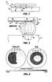
- FIG. 1is a cross-sectional side view of an integrated circuit in a flip-chip package
- FIG. 2is a cross-sectional side view of a portion of a flip-chip assembly illustrating a single solder bump
- FIG. 3Ais a cross-sectional side view of the components included in a single bump junction of the flip-chip assembly of FIG. 1 ;
- FIG. 3Bis a cross-sectional front view of the bump junction of FIG. 3A ;
- FIG. 3Cis an isometric view of the bump junction of FIG. 3A ;
- FIG. 3Dis a top plan view of the bump junction of FIG. 3A ;
- FIG. 3Eis a perspective view of the trace and pad of FIGS. 3A-3D ;
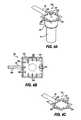
- FIG. 4Ais an isometric view of the components included in a single bump junction of a flip-chip assembly as implemented in accordance with the invention
- FIG. 4Bis a top plan view of the bump junction of FIG. 4B ;
- FIG. 4Cis a perspective view of the trace and pad of FIGS. 4A-4B ;
- FIG. 5is a pair of graphs illustrating the current density within a bump at the junction with the UBM of a prior art flip-chip assembly and at the same location when implemented in accordance with the invention
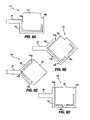
- FIGS. 6A through 6Dare plan views of alternative embodiments of the invention of pads and associated trace routes that seek to produce a radially uniform inflow of current into the pad and joint attached thereto;
- FIG. 7is an operational flowchart of a method for determining trace widths of conductive leads connecting the outer channel to the inner pad of a pad implemented according to the invention
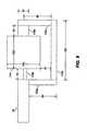
- FIG. 8is a plan view of an example pad of the invention partitioned into trace segments with associated dimensions for use in determining the trace widths of the conductive leads;
- FIG. 9is top plan view of a bump junction employing a plurality of sub-traces for a single trace in accordance with an embodiment of the present invention.
- FIG. 10is top plan view of another embodiment of the bump junction employing a plurality of sub-traces for a single trace
- FIG. 11is a partial detail view of the sub-traces employed in the embodiment shown in FIG. 9 ;
- FIG. 12is a partial detail view of the sub-traces employed in the embodiment shown in FIG. 10 ;
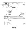
- FIG. 13Ais a cross-sectional side view of a portion of a bump junction configured in several layers and FIG. 13B is a top plan view of each of the layers employed in FIG. 13A ;
- FIG. 14Ais a cross-sectional side view of a portion of a bump junction configured in two layers and FIG. 14B is a top plan view of each of the layers employed in FIG. 14A ;
- FIG. 15Ais a cross-sectional side view of a portion of a bump junction configured in several layers and FIG. 15B is a top plan view of each of the layers employed in FIG. 15A .
- a novel trace routing design for integrated circuit I/O padsis described in detail below that seeks to introduce current flow delivered by a trace into an integrated circuit pad by routing current flow from the trace delivering the current to the pad through a plurality of traces to the pad or through an intermediate trace channel and multiple conductive leads to the pad. Current is therefore introduced to the pad from a number of different paths rather than the single path that results from a direct connection between the trace and pad.
- FIGS. 3A , 3 B, 3 C, 3 D, 3 E, and 3 Fthe configuration of a traditional prior art solder bump in a flip-chip assembly is shown in FIGS. 3A , 3 B, 3 C, 3 D, 3 E, and 3 F. More particularly, FIG. 3A is a cross-sectional side view, FIG. 3B is a cross-sectional front view, FIG.
- FIG. 3Cis an isometric view
- FIG. 3Dis a top plan view of the components included in a single bump junction of the flip-chip assembly 10 of FIG. 1
- FIG. 3Eis a perspective view of the trace 20 and pad 22 of FIGS. 3A-3D .
- the trace 20is conductively connected to the pad 22 on the outermost trace layer of the integrated circuit 14 (of FIG. 1 ).
- the pad 22is capped with a passivation layer 24 , typically comprising either a nitride or a polymer.
- An opening 25is etched into the passivation layer 24 and the UBM 26 is plated over both the opening 25 and a portion of the passivation layer 24 .
- solderattaches to the UBM 26 during the bumping process to form bump 16 , which conductively connects the UBM 26 and the substrate pad 28 when the die is flipped and attached to the substrate 12 .
- the substrate pad 28is connected to substrate via 30 for routing to circuitry implemented on or otherwise connected to the substrate 12 .
- the metal layers M 1 , . . . , Mn, vias, and UBMare implemented using highly conductive material, typically copper, gold, or other elements or compounds of high conductivity.
- the dielectric layers D 1 , . . . , Dn- 1 and 48are typically implemented using a polymer such as Benzoclyclobutene (BCB).
- the bump 16 materialis typically copper or a lead solder compound such as PbSn, AuPb, PbAg, etc.
- the trace 20is instead connected to an outer trace channel 102 , which is connected to multiple conductive trace leads 106 that connect the outer trace channel 102 and the pad 104 .
- the impedance of the multiple conductive leads 106may be respectively customized to achieve a relatively uniform current distribution seen on the pad 22 . Impedance tailoring of the various conductive leads is reflected in the various widths of the conductive trace leads. A methodology for determining the widths of the leads is described hereinafter.
- current delivered by the trace 20flows into the outer trace channel 102 , as indicated by the dotted arrows 108 illustrated in FIG. 4B , and is routed through the outer trace channel 102 to and through the plurality of conductive trace leads 106 , and into the pad 104 .
- the respective resistances of the plurality of conductive conductive trace leads 106are preferably implemented by design to distribute equal current flow (within a reasonable margin of error) through each lead 106 , thereby producing a more uniform current density on the pad 104 and in a bump 16 connected to the pad 104 .
- FIG. 5presents graphs showing for comparison the current density for a bump 16 coupled to the traditional integrated circuit pad 22 of FIGS. 3A-3E , and the current density for a bump 16 coupled to a pad coupled to a current delivering trace using the trace routing design of the invention of FIGS. 4A-4C .
- the embodiment of the trace routing design of the invention shown in FIGS. 4A-4Cresults in a 40% reduction in overall maximum current density.
- current crowdingoccurs in the area of the bump 16 closest to connection of the trace 20 to the pad 22 and directly below the portion of the UBM within the opening 25 .
- the currentis distributed substantially equally around the area near the outer circumference of the opening 25 between the pad 104 and the UBM 26 on the bump 16 , resulting in a lower maximum current density across the bump, and therefore eliminating or significantly reducing any current crowding.
- the methodology of the inventiondoes not address the intensification of current due to turning effects, a lower value of current density is obtained in the bump 16 due to the use of a plurality of conducive leads 106 to introduce the current to the bump 16 at multiple locations.
- the invention based designhas a current density which is 40% that of the traditional design.
- the exponent, nmay have values between 1 and 2
- the invention-based designwill have predicted electromigration lives that are 2.5 to 6.25 times greater than that of the traditional configuration.
- FIGS. 6A through 6Drespectively illustrate alternative illustrative embodiments of trace routing designs implemented according to the principles of the invention.
- FIG. 6Aillustrates a trace routing design 110 that includes an outer channel 112 that routes current around half of the inner pad 114 to introduce current flow through two conductive leads 116 a and 116 b on opposite sides of the pad.
- FIG. 6Billustrates a trace routing design 120 that includes an outer channel 122 that routes current five-eighths of the way around the pad 124 in one direction and an eighth of the way around the pad 124 in the other direction, and includes four conductive leads 126 a, 126 b, 126 c, 126 d for introducing current to the pad 124 .
- FIG. 1illustrates a trace routing design 110 that includes an outer channel 112 that routes current around half of the inner pad 114 to introduce current flow through two conductive leads 116 a and 116 b on opposite sides of the pad.
- FIG. 6Billustrates a trace routing design 120 that includes an
- FIG. 6Cillustrates a trace routing design 130 that includes an outer channel 132 that routes current a quarter of the distance around the pad 134 in two different directions, and includes three conductive leads 136 a, 136 b, 136 c for introducing current to the pad 134 .
- FIG. 6Dillustrates a trace routing design 140 that includes an outer channel 142 that routes current five-eighths of the way around the pad 144 in one direction and an eighth of the way around the pad 144 in the other direction, and includes four conductive leads 146 a, 146 b, 146 c, 146 d for introducing current to the pad 144 .
- the trace routing designis not dependent on the orientation of the inner pad, the junction point of the main current delivering trace connection to the outer channel, the number of conductive leads connecting the outer channel to the inner pad, or the path of the outer channel.
- Different improvementsmay be obtained for configurations other than those illustrated.
- symmetryis not a required attribute of the invention, nor is any particular number of conductive leads.
- the inventionis to introduce the current into the pad from multiple locations such that a reasonably uniform current density is achieved at the bump. In some configurations this will translate to equalizing the current flowing through each of the conductive leads to the pad. In other configurations the currents flow needs to be set up to allow flow in proportions other than equal proportion.
- the respective impedances of the conductive leadse.g., through adjusting the widths of the conductive trace leads assuming a constant trace thickness
- FIG. 7is an operational flowchart illustrating a methodology for determining trace widths of conductive leads connecting the outer channel 102 to the inner pad 104 .
- the method illustratedis limited to application of non-branching outer channels (e.g., the trace routing design of FIG. 6A ) of constant width and thickness.
- the methodincludes the step of obtaining the trace thickness, for each conductive lead to be implemented, obtaining the length and width of the outer channel from the trace junction of the pad 100 to the junction of the conductive lead (step 201 ).
- the width of one of the conductive leadsis selected or obtained (step 202 ).
- each remaining conductive lead(determined in step 203 ), one of the remaining conductive leads is selected (step 204 ), and the width of the selected remaining conductive lead is calculated such that the ratio of the width of the selected remaining conductive lead to the length of the selected remaining conductive lead (obtained in step 201 ) is substantially equal to the ratio of the known width of the first conductive lead to the known length of the first conductive lead ( 205 ).
- the calculation for branching tracese.g., the trace routing designs of FIGS. 4A through 4C and 6 B through 6 D) or those with non-constant geometry follows basic circuit theory where the resistances for each path are tailored such that the current flowing into the pad is the same for all branches. This calculation will be obvious to those skilled in simple resistive circuit theory.
- FIG. 8illustrates the two-conductive lead trace design 110 where the outer channel 112 is partitioned into trace segments. Suppose that the width w, thickness t, and resistivity ⁇ of the channel 112 are all constant. Then, suppose the width of conductive lead 116 b is selected to be 10 um.
- a trace configuration employing a plurality of sub-traces for a single traceis provided.
- a single trace 300 for delivering current to a generally rectangular bump pad 302is divided into a plurality of sub-traces 304 .
- element 306is provided to represent an equipotential point of the joint connection; element 306 may in certain embodiments represent a source/sink.
- currentis uniformly distributed across each side 308 , 310 of the bump pad 302 .
- a rectangular padis shown it is to be appreciated that other shaped pads may be employed for example octagonal, triangular, etc. or any other shape that includes at least two planar sides for coupling the sub-traces to in a uniform manner.
- the sub-traces 304 and pad 302are in the same plane, i.e. the redistribution layer (RDL).
- the dotted boxrepresents a solid metal pad, hence the sub-traces 304 traces connect to the pad 302 and terminate at the pad edge, e.g., edge 308 and edge 310 , similar to the RDL layer shown in FIG. 14A .
- the sub-traces 304are in another layer similar to layer M 8 shown in FIG. 15A .
- viasconnect the traces “down” to the pad at locations where the traces overlie the pad. The interconnecting of layers with vias will be described below in relation to FIGS. 13-15 .
- the individual sub-traces 304are dimensioned so each trace will have an equal resistance.
- the inner sub-tracewill be of shorter length and less width than the outer sub-trace while resulting in the same resistance. That is, the resistance of each trace is substantially the same.
- the goal of having each sub-trace deliver the same currentcan be achieved by making the resistance of each sub-trace the same. Assuming that each sub-trace is a straight line (i.e., ignoring corners where the sub-trace changes direction) then the resistance of the sub-trace is resistivity*length/width*thickness.
- a power bus 312surrounds the bump pad 302 in a U-shaped configuration and a plurality of sub-traces 314 lie within the power bus 312 .
- Currentwill enter the bump pad 302 from side 318 closest to the power bus 312 and from a side opposite 316 the power bus.
- the bump pad 302is disposed a distance d from the power bus 312 .
- the pad 302is disposed from the power bus the distance d to equalize the current entering both sides 316 , 318 of the pad 302 .
- the length/width ratio of sub-trace 314 to the left of the pad 320 in FIG. 10should be substantially equal to the length/width ratio of the bus+d/width of sub-trace 314 on the right.
- FIG. 11is a partial detail view of the sub-traces employed in the embodiment shown in FIG. 9 and FIG. 12 is a partial detail view of the sub-traces employed in the embodiment shown in FIG. 10 .
- the pad 302is 80 um square and the pitch is 200 um. So the total length of the 3.4 um sub-trace 303 is 65 um+3 um (going along the center line) and the total length of the 8.9 um sub-trace 305 is 135 um+45.5 um.
- the resistances for sub-trace 303 and sub-race 305are within a predetermined tolerance. However, the resistance values are substantially the same if the effect of the corner in each sub-trace is included.
- FIG. 13Ais a cross-sectional side view of a portion of a bump junction configured in several layers and FIG. 13B is a top plan view of each of the layers employed in FIG. 13A .
- the bump padis disposed in the redistribution layer RDL
- sub-traces 304are disposed in metal layer M 8
- sub-traces 314are disposed in metal layer M 7 .
- the layers shownare for illustration only and the sub-traces may lie in other layers of the chip.
- a first plurality of vias 320extend from the sub-traces 304 in metal layer M 8 to the bump pad 302 .
- a second plurality of vias 322are provided which extend from the sub-traces 314 in metal layer M 7 to cross-over points in metal layer M 8 .
- Cross-over pointsmean where one entity is directly over/under another.
- Vias 320extend from the sub-traces 304 in the layer M 8 to the pad 302 only in the dashed box. These vias 320 will couple to the pad 302 in 7 rectangular shaped regions over the dashed box. From layer M 7 to layer M 8 , the vias 322 will only be where the 8 M 7 sub-traces 314 overlay the 7 M 8 sub-traces 304 , resulting in 56 square shaped areas with vias 322 . In this embodiment, vias only connect adjacent layers.
- the plurality of vias 320will terminate substantially over the face of the bump pad thereby providing a uniform distribution of current over the pad 302 . It is further to be appreciated that the number of vias 320 employed would depend on the diameter of each vias (e.g., each via being a cylinder), the minimum placement pitch and the width of each of the sub-traces 304 and 314 .
- the embodiment shown in FIGS. 13A and 13Brepresent a power grid, which has traces or sub-traces going one way on one level and an orthogonal direction on the next. In general, current limits in the traces require dividing the current through multiple layers of metal.
- FIG. 14Ais a cross-sectional side view of a portion of a bump junction configured in two layers and FIG. 14B is a top plan view of each of the layers employed in FIG. 14A .
- the bump pad 302 and sub-traces 304are disposed in the redistribution layer RDL and sub-traces 314 are disposed in metal layer M 8 .
- the layers shownare for illustration only and the sub-traces may lie in other layers of the chip.
- sub-traces 304are directly coupled to two sides 308 , 310 of bump pad 302 .
- the first plurality of vias 320extend from the sub-traces 314 in metal layer M 8 to the bump pad 302 . In this manner, current enters the pad 302 over the face or top portion of the pad through the vias 320 and current enters through at least two sides via sub-traces 304 thereby providing a uniform current density over the pad.
- FIG. 15Ais a cross-sectional side view of a portion of a bump junction configured in several layers and FIG. 15B is a top plan view of each of the layers employed in FIG. 15A .
- the bump pad 302is disposed in the redistribution layer RDL and sub-traces 314 are disposed in metal layer M 8 . It is to be appreciated that the layers shown are for illustration only and the sub-traces may lie in other layers of the chip.
- the first plurality of vias 320extend from the sub-traces 314 in metal layer M 8 to the bump pad 302 . In this manner, current enters the pad 302 over the face or top portion of the pad through the vias 320 thereby providing a uniform current density over the pad.
- connection of the vias 320 to the pad 302lies in a via region 344 which is within the footprint of the pad opening 25 .
- the “footprint”is coaxial with the pad opening 25 , and is identical in both shape and orientation to the pad opening 25 .
- the selection of the number of vias 320 within the via region 344 as well as the selection of the relative area of the via region 344 with respect to that of the opening 25dictate the maximum current density within the bump 16 .
- the vias 320will be placed with 80% of the diameter of the opening 25 .
- the vias 320provide two benefits. The first is that the impedances/resistances of the vias 320 , which may be adjusted during the design phase to obtain a desirable current distribution, causes current flow passing from the traces 314 to enter the pad 302 uniformly, thereby reducing the current crowding at an edge of the pad as in the prior art.
- the second benefit of the vias 320is that when the vias 320 are positioned for connection within the footprint of the pad opening 25 (i.e., the footprint of the outer-pad-to-UBM interface), adverse current concentration effects that occur when current enters the outer pad opening 25 to the UBM 26 from a radial location outside the footprint of the outer pad opening 25 are minimized.
Landscapes
- Engineering & Computer Science (AREA)
- Computer Hardware Design (AREA)
- Microelectronics & Electronic Packaging (AREA)
- Power Engineering (AREA)
- Physics & Mathematics (AREA)
- Condensed Matter Physics & Semiconductors (AREA)
- General Physics & Mathematics (AREA)
- Internal Circuitry In Semiconductor Integrated Circuit Devices (AREA)
- Semiconductor Integrated Circuits (AREA)
- Design And Manufacture Of Integrated Circuits (AREA)
- Wire Bonding (AREA)
Abstract
Description
where A incorporates the effects of temperature and other factors and the power n is in the range of 1 to 2 for lead solders. High local values of the current density, J, may cause failures that are premature in time when compared with the failures that occur when the current is uniformly distributed in the
resistivity*length/width*thickness.
For straight sub-traces in a given layer, i.e., sub-traces without any turns, the resistivity and thickness are constants, so the resistance of a sub-race in a layer is proportional to a length/width ratio. To make equal resistance traces in a specific layer:
length—1/width—1=length—2/width—2.
Exemplary sub-trace widths are indicated in
R(3.4 um)=(65+3)/3.4=20
R(8.9 um)=(135+45.5)/8.9=20.2.
The resistances for
Claims (8)
Priority Applications (1)
| Application Number | Priority Date | Filing Date | Title |
|---|---|---|---|
| US11/779,833US7659622B2 (en) | 2005-02-01 | 2007-07-18 | Trace design to minimize electromigration damage to solder bumps |
Applications Claiming Priority (2)
| Application Number | Priority Date | Filing Date | Title |
|---|---|---|---|
| US11/047,887US7253528B2 (en) | 2005-02-01 | 2005-02-01 | Trace design to minimize electromigration damage to solder bumps |
| US11/779,833US7659622B2 (en) | 2005-02-01 | 2007-07-18 | Trace design to minimize electromigration damage to solder bumps |
Related Parent Applications (1)
| Application Number | Title | Priority Date | Filing Date |
|---|---|---|---|
| US11/047,887Continuation-In-PartUS7253528B2 (en) | 2005-02-01 | 2005-02-01 | Trace design to minimize electromigration damage to solder bumps |
Publications (2)
| Publication Number | Publication Date |
|---|---|
| US20080042271A1 US20080042271A1 (en) | 2008-02-21 |
| US7659622B2true US7659622B2 (en) | 2010-02-09 |
Family
ID=36907804
Family Applications (2)
| Application Number | Title | Priority Date | Filing Date |
|---|---|---|---|
| US11/047,887Active2026-02-02US7253528B2 (en) | 2005-02-01 | 2005-02-01 | Trace design to minimize electromigration damage to solder bumps |
| US11/779,833Expired - Fee RelatedUS7659622B2 (en) | 2005-02-01 | 2007-07-18 | Trace design to minimize electromigration damage to solder bumps |
Family Applications Before (1)
| Application Number | Title | Priority Date | Filing Date |
|---|---|---|---|
| US11/047,887Active2026-02-02US7253528B2 (en) | 2005-02-01 | 2005-02-01 | Trace design to minimize electromigration damage to solder bumps |
Country Status (3)
| Country | Link |
|---|---|
| US (2) | US7253528B2 (en) |
| CN (1) | CN100541772C (en) |
| TW (1) | TWI278085B (en) |
Cited By (13)
| Publication number | Priority date | Publication date | Assignee | Title |
|---|---|---|---|---|
| US8656333B1 (en)* | 2010-02-16 | 2014-02-18 | Deca Technologies, Inc. | Integrated circuit package auto-routing |
| US8826203B2 (en) | 2012-06-18 | 2014-09-02 | International Business Machines Corporation | Automating current-aware integrated circuit and package design and optimization |
| US8826221B2 (en) | 2010-02-16 | 2014-09-02 | Deca Technologies Inc. | Adaptive patterning for panelized packaging |
| US8826216B2 (en) | 2012-06-18 | 2014-09-02 | International Business Machines Corporation | Token-based current control to mitigate current delivery limitations in integrated circuits |
| US8863068B2 (en) | 2012-06-18 | 2014-10-14 | International Business Machines Corporation | Current-aware floorplanning to overcome current delivery limitations in integrated circuits |
| US8914764B2 (en) | 2012-06-18 | 2014-12-16 | International Business Machines Corporation | Adaptive workload based optimizations coupled with a heterogeneous current-aware baseline design to mitigate current delivery limitations in integrated circuits |
| US9040316B1 (en) | 2014-06-12 | 2015-05-26 | Deca Technologies Inc. | Semiconductor device and method of adaptive patterning for panelized packaging with dynamic via clipping |
| US9141159B2 (en) | 2011-11-03 | 2015-09-22 | International Business Machines Corporation | Minimizing aggregate cooling and leakage power with fast convergence |
| US9196509B2 (en) | 2010-02-16 | 2015-11-24 | Deca Technologies Inc | Semiconductor device and method of adaptive patterning for panelized packaging |
| US9477568B2 (en) | 2013-09-27 | 2016-10-25 | International Business Machines Corporation | Managing interconnect electromigration effects |
| US10157803B2 (en) | 2016-09-19 | 2018-12-18 | Deca Technologies Inc. | Semiconductor device and method of unit specific progressive alignment |
| US10573601B2 (en) | 2016-09-19 | 2020-02-25 | Deca Technologies Inc. | Semiconductor device and method of unit specific progressive alignment |
| US12362322B2 (en) | 2023-06-22 | 2025-07-15 | Deca Technologies Usa, Inc. | Method of making a fan-out semiconductor assembly with an intermediate carrier |
Families Citing this family (17)
| Publication number | Priority date | Publication date | Assignee | Title |
|---|---|---|---|---|
| US7253528B2 (en) | 2005-02-01 | 2007-08-07 | Avago Technologies General Ip Pte. Ltd. | Trace design to minimize electromigration damage to solder bumps |
| US7208843B2 (en)* | 2005-02-01 | 2007-04-24 | Avago Technologies General Ip (Singapore) Pte. Ltd. | Routing design to minimize electromigration damage to solder bumps |
| US7911803B2 (en)* | 2007-10-16 | 2011-03-22 | International Business Machines Corporation | Current distribution structure and method |
| US7812462B2 (en)* | 2008-11-04 | 2010-10-12 | National Semiconductor Corporation | Conductive paths for transmitting an electrical signal through an electrical connector |
| US8084858B2 (en) | 2009-04-15 | 2011-12-27 | International Business Machines Corporation | Metal wiring structures for uniform current density in C4 balls |
| TWI528514B (en)* | 2009-08-20 | 2016-04-01 | 精材科技股份有限公司 | Chip package and fabrication method thereof |
| US8446006B2 (en)* | 2009-12-17 | 2013-05-21 | International Business Machines Corporation | Structures and methods to reduce maximum current density in a solder ball |
| US9214385B2 (en) | 2009-12-17 | 2015-12-15 | Globalfoundries Inc. | Semiconductor device including passivation layer encapsulant |
| US8492892B2 (en) | 2010-12-08 | 2013-07-23 | International Business Machines Corporation | Solder bump connections |
| US8531030B2 (en)* | 2010-12-16 | 2013-09-10 | Texas Instruments Incorporated | IC device having electromigration resistant feed line structures |
| US20120178189A1 (en)* | 2011-01-06 | 2012-07-12 | Reber Douglas M | Method for forming an over pad metalization (opm) on a bond pad |
| US8928110B2 (en) | 2011-09-09 | 2015-01-06 | United Microelectronics Corp. | Dummy cell pattern for improving device thermal uniformity |
| US8835996B2 (en) | 2011-12-28 | 2014-09-16 | United Microelectronics Corporation | Integrated circuit configuration having extension conductor structure and fabricating method thereof |
| US8434030B1 (en) | 2012-01-05 | 2013-04-30 | United Microelectronics Corporation | Integrated circuit design and fabrication method by way of detecting and scoring hotspots |
| US9515035B2 (en) | 2014-12-19 | 2016-12-06 | International Business Machines Corporation | Three-dimensional integrated circuit integration |
| CN105118798B (en)* | 2015-08-26 | 2018-05-04 | 上海华力微电子有限公司 | Electro-migration testing structure and test method |
| FR3050570A1 (en)* | 2016-04-21 | 2017-10-27 | Commissariat Energie Atomique | MULTI-LEVEL ELECTRICAL INTERCONNECTION STRUCTURE WITH OPTIMIZED CURRENT DENSITY DISTRIBUTION |
Citations (16)
| Publication number | Priority date | Publication date | Assignee | Title |
|---|---|---|---|---|
| US4654692A (en) | 1983-06-30 | 1987-03-31 | Kabushiki Kaisha Toshiba | Semiconductor device of resin-seal type |
| US5289036A (en) | 1991-01-22 | 1994-02-22 | Nec Corporation | Resin sealed semiconductor integrated circuit |
| US5461260A (en) | 1994-08-01 | 1995-10-24 | Motorola Inc. | Semiconductor device interconnect layout structure for reducing premature electromigration failure due to high localized current density |
| US5777486A (en) | 1994-10-03 | 1998-07-07 | United Microelectronics Corporation | Electromigration test pattern simulating semiconductor components |
| US6504252B2 (en) | 2000-12-27 | 2003-01-07 | Kabushiki Kaisha Toshiba | Semiconductor device with a split pad electrode |
| US6521996B1 (en) | 2000-06-30 | 2003-02-18 | Intel Corporation | Ball limiting metallurgy for input/outputs and methods of fabrication |
| US20030167632A1 (en) | 2002-03-06 | 2003-09-11 | Stmicroelectronics, Inc. | System and method for providing a redistribution metal layer in an integrated circuit |
| US20040004227A1 (en)* | 2002-07-04 | 2004-01-08 | Kiyoshi Tateishi | Unit for driving light-emitting device |
| US20040113261A1 (en) | 2002-12-03 | 2004-06-17 | Shinko Electric Industries Co., Ltd., | Electronic parts packaging structure and method of manufacturing the same |
| US6818996B2 (en) | 2002-12-20 | 2004-11-16 | Lsi Logic Corporation | Multi-level redistribution layer traces for reducing current crowding in flipchip solder bumps |
| US6825541B2 (en) | 2002-10-09 | 2004-11-30 | Taiwan Semiconductor Manufacturing Co., Ltd | Bump pad design for flip chip bumping |
| US20050040527A1 (en) | 2003-08-21 | 2005-02-24 | Min-Lung Huang | [chip structure] |
| US20060043608A1 (en) | 2004-08-31 | 2006-03-02 | International Business Machines Corporation | Low stress conductive polymer bump |
| US7081405B2 (en) | 2002-03-06 | 2006-07-25 | Via Technologies, Inc. | Package module for an IC device and method of forming the same |
| US20060186539A1 (en) | 2005-02-01 | 2006-08-24 | Dauksher Walter J | Trace design to minimize electromigration damage to solder bumps |
| US7208843B2 (en) | 2005-02-01 | 2007-04-24 | Avago Technologies General Ip (Singapore) Pte. Ltd. | Routing design to minimize electromigration damage to solder bumps |
- 2005
- 2005-02-01USUS11/047,887patent/US7253528B2/enactiveActive
- 2005-08-17TWTW094128009Apatent/TWI278085B/ennot_activeIP Right Cessation
- 2005-12-22CNCNB2005101322624Apatent/CN100541772C/ennot_activeExpired - Fee Related
- 2007
- 2007-07-18USUS11/779,833patent/US7659622B2/ennot_activeExpired - Fee Related
Patent Citations (16)
| Publication number | Priority date | Publication date | Assignee | Title |
|---|---|---|---|---|
| US4654692A (en) | 1983-06-30 | 1987-03-31 | Kabushiki Kaisha Toshiba | Semiconductor device of resin-seal type |
| US5289036A (en) | 1991-01-22 | 1994-02-22 | Nec Corporation | Resin sealed semiconductor integrated circuit |
| US5461260A (en) | 1994-08-01 | 1995-10-24 | Motorola Inc. | Semiconductor device interconnect layout structure for reducing premature electromigration failure due to high localized current density |
| US5777486A (en) | 1994-10-03 | 1998-07-07 | United Microelectronics Corporation | Electromigration test pattern simulating semiconductor components |
| US6521996B1 (en) | 2000-06-30 | 2003-02-18 | Intel Corporation | Ball limiting metallurgy for input/outputs and methods of fabrication |
| US6504252B2 (en) | 2000-12-27 | 2003-01-07 | Kabushiki Kaisha Toshiba | Semiconductor device with a split pad electrode |
| US20030167632A1 (en) | 2002-03-06 | 2003-09-11 | Stmicroelectronics, Inc. | System and method for providing a redistribution metal layer in an integrated circuit |
| US7081405B2 (en) | 2002-03-06 | 2006-07-25 | Via Technologies, Inc. | Package module for an IC device and method of forming the same |
| US20040004227A1 (en)* | 2002-07-04 | 2004-01-08 | Kiyoshi Tateishi | Unit for driving light-emitting device |
| US6825541B2 (en) | 2002-10-09 | 2004-11-30 | Taiwan Semiconductor Manufacturing Co., Ltd | Bump pad design for flip chip bumping |
| US20040113261A1 (en) | 2002-12-03 | 2004-06-17 | Shinko Electric Industries Co., Ltd., | Electronic parts packaging structure and method of manufacturing the same |
| US6818996B2 (en) | 2002-12-20 | 2004-11-16 | Lsi Logic Corporation | Multi-level redistribution layer traces for reducing current crowding in flipchip solder bumps |
| US20050040527A1 (en) | 2003-08-21 | 2005-02-24 | Min-Lung Huang | [chip structure] |
| US20060043608A1 (en) | 2004-08-31 | 2006-03-02 | International Business Machines Corporation | Low stress conductive polymer bump |
| US20060186539A1 (en) | 2005-02-01 | 2006-08-24 | Dauksher Walter J | Trace design to minimize electromigration damage to solder bumps |
| US7208843B2 (en) | 2005-02-01 | 2007-04-24 | Avago Technologies General Ip (Singapore) Pte. Ltd. | Routing design to minimize electromigration damage to solder bumps |
Cited By (19)
| Publication number | Priority date | Publication date | Assignee | Title |
|---|---|---|---|---|
| US9887103B2 (en) | 2010-02-16 | 2018-02-06 | Deca Technologies, Inc. | Semiconductor device and method of adaptive patterning for panelized packaging |
| US8826221B2 (en) | 2010-02-16 | 2014-09-02 | Deca Technologies Inc. | Adaptive patterning for panelized packaging |
| US9520331B2 (en) | 2010-02-16 | 2016-12-13 | Deca Technologies Inc. | Adaptive patterning for panelized packaging |
| US8656333B1 (en)* | 2010-02-16 | 2014-02-18 | Deca Technologies, Inc. | Integrated circuit package auto-routing |
| US9418905B2 (en) | 2010-02-16 | 2016-08-16 | Deca Technologies Inc. | Adaptive patterning for panelized packaging |
| US9196509B2 (en) | 2010-02-16 | 2015-11-24 | Deca Technologies Inc | Semiconductor device and method of adaptive patterning for panelized packaging |
| US9146597B2 (en) | 2011-11-03 | 2015-09-29 | International Business Machines Corporation | Minimizing aggregate cooling and leakage power with fast convergence |
| US9141159B2 (en) | 2011-11-03 | 2015-09-22 | International Business Machines Corporation | Minimizing aggregate cooling and leakage power with fast convergence |
| US8863068B2 (en) | 2012-06-18 | 2014-10-14 | International Business Machines Corporation | Current-aware floorplanning to overcome current delivery limitations in integrated circuits |
| US8914764B2 (en) | 2012-06-18 | 2014-12-16 | International Business Machines Corporation | Adaptive workload based optimizations coupled with a heterogeneous current-aware baseline design to mitigate current delivery limitations in integrated circuits |
| US8826216B2 (en) | 2012-06-18 | 2014-09-02 | International Business Machines Corporation | Token-based current control to mitigate current delivery limitations in integrated circuits |
| US8826203B2 (en) | 2012-06-18 | 2014-09-02 | International Business Machines Corporation | Automating current-aware integrated circuit and package design and optimization |
| US9477568B2 (en) | 2013-09-27 | 2016-10-25 | International Business Machines Corporation | Managing interconnect electromigration effects |
| US9040316B1 (en) | 2014-06-12 | 2015-05-26 | Deca Technologies Inc. | Semiconductor device and method of adaptive patterning for panelized packaging with dynamic via clipping |
| US9397069B2 (en) | 2014-06-12 | 2016-07-19 | Deca Technologies Inc. | Semiconductor device and method of adaptive patterning for panelized packaging with dynamic via clipping |
| US9978655B2 (en) | 2014-06-12 | 2018-05-22 | Deca Technologies Inc. | Semiconductor device and method of adaptive patterning for panelized packaging with dynamic via clipping |
| US10157803B2 (en) | 2016-09-19 | 2018-12-18 | Deca Technologies Inc. | Semiconductor device and method of unit specific progressive alignment |
| US10573601B2 (en) | 2016-09-19 | 2020-02-25 | Deca Technologies Inc. | Semiconductor device and method of unit specific progressive alignment |
| US12362322B2 (en) | 2023-06-22 | 2025-07-15 | Deca Technologies Usa, Inc. | Method of making a fan-out semiconductor assembly with an intermediate carrier |
Also Published As
| Publication number | Publication date |
|---|---|
| US7253528B2 (en) | 2007-08-07 |
| CN1815725A (en) | 2006-08-09 |
| CN100541772C (en) | 2009-09-16 |
| US20080042271A1 (en) | 2008-02-21 |
| US20060186539A1 (en) | 2006-08-24 |
| TW200629506A (en) | 2006-08-16 |
| TWI278085B (en) | 2007-04-01 |
Similar Documents
| Publication | Publication Date | Title |
|---|---|---|
| US7659622B2 (en) | Trace design to minimize electromigration damage to solder bumps | |
| KR101140469B1 (en) | A routing design to minimize electromigration damage to solder bumps | |
| US8212357B2 (en) | Combination via and pad structure for improved solder bump electromigration characteristics | |
| US10256189B2 (en) | Switched power stage with integrated passive components | |
| US8361598B2 (en) | Substrate anchor structure and method | |
| CN110970387B (en) | Semiconductor device and method of forming semiconductor device | |
| US8531030B2 (en) | IC device having electromigration resistant feed line structures | |
| US7268433B2 (en) | Semiconductor device | |
| KR20060084793A (en) | Semiconductor device and its assembly | |
| US7180195B2 (en) | Method and apparatus for improved power routing | |
| US6818996B2 (en) | Multi-level redistribution layer traces for reducing current crowding in flipchip solder bumps | |
| US20030042619A1 (en) | Configuration of conductive bumps and redistribution layer on a flip chip | |
| US6686615B1 (en) | Flip-chip type semiconductor device for reducing signal skew | |
| US6822327B1 (en) | Flip-chip interconnected with increased current-carrying capability | |
| US6770554B1 (en) | On-chip interconnect circuits with use of large-sized copper fill in CMP process | |
| US7812462B2 (en) | Conductive paths for transmitting an electrical signal through an electrical connector | |
| JP7715477B2 (en) | Interconnects for Electronic Devices | |
| US7208830B2 (en) | Interconnect shunt used for current distribution and reliability redundancy | |
| US20240063118A1 (en) | Back end of line structure for improved current density in hr devices |
Legal Events
| Date | Code | Title | Description |
|---|---|---|---|
| AS | Assignment | Owner name:AVAGO TECHNOLOGIES GENERAL IP (SINGAPORE) PTE. LTD Free format text:ASSIGNMENT OF ASSIGNORS INTEREST;ASSIGNORS:DAUKSHER, WALTER J., MR.;EATON, DENNIS H., MR.;REEL/FRAME:019572/0270 Effective date:20070718 | |
| STCF | Information on status: patent grant | Free format text:PATENTED CASE | |
| FPAY | Fee payment | Year of fee payment:4 | |
| AS | Assignment | Owner name:DEUTSCHE BANK AG NEW YORK BRANCH, AS COLLATERAL AGENT, NEW YORK Free format text:PATENT SECURITY AGREEMENT;ASSIGNOR:AVAGO TECHNOLOGIES GENERAL IP (SINGAPORE) PTE. LTD.;REEL/FRAME:032851/0001 Effective date:20140506 Owner name:DEUTSCHE BANK AG NEW YORK BRANCH, AS COLLATERAL AG Free format text:PATENT SECURITY AGREEMENT;ASSIGNOR:AVAGO TECHNOLOGIES GENERAL IP (SINGAPORE) PTE. LTD.;REEL/FRAME:032851/0001 Effective date:20140506 | |
| AS | Assignment | Owner name:AVAGO TECHNOLOGIES GENERAL IP (SINGAPORE) PTE. LTD., SINGAPORE Free format text:TERMINATION AND RELEASE OF SECURITY INTEREST IN PATENT RIGHTS (RELEASES RF 032851-0001);ASSIGNOR:DEUTSCHE BANK AG NEW YORK BRANCH, AS COLLATERAL AGENT;REEL/FRAME:037689/0001 Effective date:20160201 Owner name:AVAGO TECHNOLOGIES GENERAL IP (SINGAPORE) PTE. LTD Free format text:TERMINATION AND RELEASE OF SECURITY INTEREST IN PATENT RIGHTS (RELEASES RF 032851-0001);ASSIGNOR:DEUTSCHE BANK AG NEW YORK BRANCH, AS COLLATERAL AGENT;REEL/FRAME:037689/0001 Effective date:20160201 | |
| AS | Assignment | Owner name:BANK OF AMERICA, N.A., AS COLLATERAL AGENT, NORTH CAROLINA Free format text:PATENT SECURITY AGREEMENT;ASSIGNOR:AVAGO TECHNOLOGIES GENERAL IP (SINGAPORE) PTE. LTD.;REEL/FRAME:037808/0001 Effective date:20160201 Owner name:BANK OF AMERICA, N.A., AS COLLATERAL AGENT, NORTH Free format text:PATENT SECURITY AGREEMENT;ASSIGNOR:AVAGO TECHNOLOGIES GENERAL IP (SINGAPORE) PTE. LTD.;REEL/FRAME:037808/0001 Effective date:20160201 | |
| AS | Assignment | Owner name:AVAGO TECHNOLOGIES GENERAL IP (SINGAPORE) PTE. LTD., SINGAPORE Free format text:TERMINATION AND RELEASE OF SECURITY INTEREST IN PATENTS;ASSIGNOR:BANK OF AMERICA, N.A., AS COLLATERAL AGENT;REEL/FRAME:041710/0001 Effective date:20170119 Owner name:AVAGO TECHNOLOGIES GENERAL IP (SINGAPORE) PTE. LTD Free format text:TERMINATION AND RELEASE OF SECURITY INTEREST IN PATENTS;ASSIGNOR:BANK OF AMERICA, N.A., AS COLLATERAL AGENT;REEL/FRAME:041710/0001 Effective date:20170119 | |
| FPAY | Fee payment | Year of fee payment:8 | |
| AS | Assignment | Owner name:AVAGO TECHNOLOGIES INTERNATIONAL SALES PTE. LIMITE Free format text:MERGER;ASSIGNOR:AVAGO TECHNOLOGIES GENERAL IP (SINGAPORE) PTE. LTD.;REEL/FRAME:047195/0827 Effective date:20180509 | |
| AS | Assignment | Owner name:AVAGO TECHNOLOGIES INTERNATIONAL SALES PTE. LIMITE Free format text:CORRECTIVE ASSIGNMENT TO CORRECT THE EFFECTIVE DATE OF MERGER PREVIOUSLY RECORDED AT REEL: 047195 FRAME: 0827. ASSIGNOR(S) HEREBY CONFIRMS THE MERGER;ASSIGNOR:AVAGO TECHNOLOGIES GENERAL IP (SINGAPORE) PTE. LTD.;REEL/FRAME:047924/0571 Effective date:20180905 | |
| AS | Assignment | Owner name:BROADCOM INTERNATIONAL PTE. LTD., SINGAPORE Free format text:ASSIGNMENT OF ASSIGNORS INTEREST;ASSIGNOR:AVAGO TECHNOLOGIES INTERNATIONAL SALES PTE. LIMITED;REEL/FRAME:053771/0901 Effective date:20200826 | |
| FEPP | Fee payment procedure | Free format text:MAINTENANCE FEE REMINDER MAILED (ORIGINAL EVENT CODE: REM.); ENTITY STATUS OF PATENT OWNER: LARGE ENTITY | |
| LAPS | Lapse for failure to pay maintenance fees | Free format text:PATENT EXPIRED FOR FAILURE TO PAY MAINTENANCE FEES (ORIGINAL EVENT CODE: EXP.); ENTITY STATUS OF PATENT OWNER: LARGE ENTITY | |
| STCH | Information on status: patent discontinuation | Free format text:PATENT EXPIRED DUE TO NONPAYMENT OF MAINTENANCE FEES UNDER 37 CFR 1.362 | |
| FP | Lapsed due to failure to pay maintenance fee | Effective date:20220209 |