US7659617B2 - Substrate for a flexible microelectronic assembly and a method of fabricating thereof - Google Patents
Substrate for a flexible microelectronic assembly and a method of fabricating thereofDownload PDFInfo
- Publication number
- US7659617B2 US7659617B2US11/606,771US60677106AUS7659617B2US 7659617 B2US7659617 B2US 7659617B2US 60677106 AUS60677106 AUS 60677106AUS 7659617 B2US7659617 B2US 7659617B2
- Authority
- US
- United States
- Prior art keywords
- substrate
- region
- dielectric
- contact elements
- traces
- Prior art date
- Legal status (The legal status is an assumption and is not a legal conclusion. Google has not performed a legal analysis and makes no representation as to the accuracy of the status listed.)
- Active, expires
Links
Images


Classifications
- H—ELECTRICITY
- H01—ELECTRIC ELEMENTS
- H01L—SEMICONDUCTOR DEVICES NOT COVERED BY CLASS H10
- H01L23/00—Details of semiconductor or other solid state devices
- H01L23/48—Arrangements for conducting electric current to or from the solid state body in operation, e.g. leads, terminal arrangements ; Selection of materials therefor
- H01L23/488—Arrangements for conducting electric current to or from the solid state body in operation, e.g. leads, terminal arrangements ; Selection of materials therefor consisting of soldered or bonded constructions
- H01L23/498—Leads, i.e. metallisations or lead-frames on insulating substrates, e.g. chip carriers
- H01L23/4985—Flexible insulating substrates
- B—PERFORMING OPERATIONS; TRANSPORTING
- B81—MICROSTRUCTURAL TECHNOLOGY
- B81B—MICROSTRUCTURAL DEVICES OR SYSTEMS, e.g. MICROMECHANICAL DEVICES
- B81B7/00—Microstructural systems; Auxiliary parts of microstructural devices or systems
- B81B7/0032—Packages or encapsulation
- B81B7/007—Interconnections between the MEMS and external electrical signals
- H—ELECTRICITY
- H01—ELECTRIC ELEMENTS
- H01L—SEMICONDUCTOR DEVICES NOT COVERED BY CLASS H10
- H01L23/00—Details of semiconductor or other solid state devices
- H01L23/02—Containers; Seals
- H01L23/04—Containers; Seals characterised by the shape of the container or parts, e.g. caps, walls
- H01L23/053—Containers; Seals characterised by the shape of the container or parts, e.g. caps, walls the container being a hollow construction and having an insulating or insulated base as a mounting for the semiconductor body
- H01L23/057—Containers; Seals characterised by the shape of the container or parts, e.g. caps, walls the container being a hollow construction and having an insulating or insulated base as a mounting for the semiconductor body the leads being parallel to the base
- H—ELECTRICITY
- H01—ELECTRIC ELEMENTS
- H01L—SEMICONDUCTOR DEVICES NOT COVERED BY CLASS H10
- H01L23/00—Details of semiconductor or other solid state devices
- H01L23/48—Arrangements for conducting electric current to or from the solid state body in operation, e.g. leads, terminal arrangements ; Selection of materials therefor
- H01L23/488—Arrangements for conducting electric current to or from the solid state body in operation, e.g. leads, terminal arrangements ; Selection of materials therefor consisting of soldered or bonded constructions
- H01L23/498—Leads, i.e. metallisations or lead-frames on insulating substrates, e.g. chip carriers
- H01L23/49861—Lead-frames fixed on or encapsulated in insulating substrates
- H—ELECTRICITY
- H05—ELECTRIC TECHNIQUES NOT OTHERWISE PROVIDED FOR
- H05K—PRINTED CIRCUITS; CASINGS OR CONSTRUCTIONAL DETAILS OF ELECTRIC APPARATUS; MANUFACTURE OF ASSEMBLAGES OF ELECTRICAL COMPONENTS
- H05K1/00—Printed circuits
- H05K1/02—Details
- H05K1/11—Printed elements for providing electric connections to or between printed circuits
- H05K1/118—Printed elements for providing electric connections to or between printed circuits specially for flexible printed circuits, e.g. using folded portions
- H—ELECTRICITY
- H05—ELECTRIC TECHNIQUES NOT OTHERWISE PROVIDED FOR
- H05K—PRINTED CIRCUITS; CASINGS OR CONSTRUCTIONAL DETAILS OF ELECTRIC APPARATUS; MANUFACTURE OF ASSEMBLAGES OF ELECTRICAL COMPONENTS
- H05K1/00—Printed circuits
- H05K1/18—Printed circuits structurally associated with non-printed electric components
- H05K1/189—Printed circuits structurally associated with non-printed electric components characterised by the use of a flexible or folded printed circuit
- B—PERFORMING OPERATIONS; TRANSPORTING
- B81—MICROSTRUCTURAL TECHNOLOGY
- B81B—MICROSTRUCTURAL DEVICES OR SYSTEMS, e.g. MICROMECHANICAL DEVICES
- B81B2207/00—Microstructural systems or auxiliary parts thereof
- B81B2207/09—Packages
- B81B2207/091—Arrangements for connecting external electrical signals to mechanical structures inside the package
- B81B2207/097—Interconnects arranged on the substrate or the lid, and covered by the package seal
- H—ELECTRICITY
- H01—ELECTRIC ELEMENTS
- H01L—SEMICONDUCTOR DEVICES NOT COVERED BY CLASS H10
- H01L2224/00—Indexing scheme for arrangements for connecting or disconnecting semiconductor or solid-state bodies and methods related thereto as covered by H01L24/00
- H01L2224/01—Means for bonding being attached to, or being formed on, the surface to be connected, e.g. chip-to-package, die-attach, "first-level" interconnects; Manufacturing methods related thereto
- H01L2224/02—Bonding areas; Manufacturing methods related thereto
- H01L2224/04—Structure, shape, material or disposition of the bonding areas prior to the connecting process
- H01L2224/05—Structure, shape, material or disposition of the bonding areas prior to the connecting process of an individual bonding area
- H01L2224/0554—External layer
- H01L2224/0556—Disposition
- H01L2224/05568—Disposition the whole external layer protruding from the surface
- H—ELECTRICITY
- H01—ELECTRIC ELEMENTS
- H01L—SEMICONDUCTOR DEVICES NOT COVERED BY CLASS H10
- H01L2224/00—Indexing scheme for arrangements for connecting or disconnecting semiconductor or solid-state bodies and methods related thereto as covered by H01L24/00
- H01L2224/01—Means for bonding being attached to, or being formed on, the surface to be connected, e.g. chip-to-package, die-attach, "first-level" interconnects; Manufacturing methods related thereto
- H01L2224/02—Bonding areas; Manufacturing methods related thereto
- H01L2224/04—Structure, shape, material or disposition of the bonding areas prior to the connecting process
- H01L2224/05—Structure, shape, material or disposition of the bonding areas prior to the connecting process of an individual bonding area
- H01L2224/0554—External layer
- H01L2224/05573—Single external layer
- H—ELECTRICITY
- H01—ELECTRIC ELEMENTS
- H01L—SEMICONDUCTOR DEVICES NOT COVERED BY CLASS H10
- H01L2224/00—Indexing scheme for arrangements for connecting or disconnecting semiconductor or solid-state bodies and methods related thereto as covered by H01L24/00
- H01L2224/01—Means for bonding being attached to, or being formed on, the surface to be connected, e.g. chip-to-package, die-attach, "first-level" interconnects; Manufacturing methods related thereto
- H01L2224/10—Bump connectors; Manufacturing methods related thereto
- H01L2224/15—Structure, shape, material or disposition of the bump connectors after the connecting process
- H01L2224/16—Structure, shape, material or disposition of the bump connectors after the connecting process of an individual bump connector
- H01L2224/161—Disposition
- H01L2224/16151—Disposition the bump connector connecting between a semiconductor or solid-state body and an item not being a semiconductor or solid-state body, e.g. chip-to-substrate, chip-to-passive
- H01L2224/16221—Disposition the bump connector connecting between a semiconductor or solid-state body and an item not being a semiconductor or solid-state body, e.g. chip-to-substrate, chip-to-passive the body and the item being stacked
- H01L2224/16225—Disposition the bump connector connecting between a semiconductor or solid-state body and an item not being a semiconductor or solid-state body, e.g. chip-to-substrate, chip-to-passive the body and the item being stacked the item being non-metallic, e.g. insulating substrate with or without metallisation
- H01L2224/16235—Disposition the bump connector connecting between a semiconductor or solid-state body and an item not being a semiconductor or solid-state body, e.g. chip-to-substrate, chip-to-passive the body and the item being stacked the item being non-metallic, e.g. insulating substrate with or without metallisation the bump connector connecting to a via metallisation of the item
- H—ELECTRICITY
- H01—ELECTRIC ELEMENTS
- H01L—SEMICONDUCTOR DEVICES NOT COVERED BY CLASS H10
- H01L2224/00—Indexing scheme for arrangements for connecting or disconnecting semiconductor or solid-state bodies and methods related thereto as covered by H01L24/00
- H01L2224/01—Means for bonding being attached to, or being formed on, the surface to be connected, e.g. chip-to-package, die-attach, "first-level" interconnects; Manufacturing methods related thereto
- H01L2224/42—Wire connectors; Manufacturing methods related thereto
- H01L2224/47—Structure, shape, material or disposition of the wire connectors after the connecting process
- H01L2224/48—Structure, shape, material or disposition of the wire connectors after the connecting process of an individual wire connector
- H01L2224/4805—Shape
- H01L2224/4809—Loop shape
- H01L2224/48091—Arched
- H—ELECTRICITY
- H01—ELECTRIC ELEMENTS
- H01L—SEMICONDUCTOR DEVICES NOT COVERED BY CLASS H10
- H01L2224/00—Indexing scheme for arrangements for connecting or disconnecting semiconductor or solid-state bodies and methods related thereto as covered by H01L24/00
- H01L2224/01—Means for bonding being attached to, or being formed on, the surface to be connected, e.g. chip-to-package, die-attach, "first-level" interconnects; Manufacturing methods related thereto
- H01L2224/42—Wire connectors; Manufacturing methods related thereto
- H01L2224/47—Structure, shape, material or disposition of the wire connectors after the connecting process
- H01L2224/48—Structure, shape, material or disposition of the wire connectors after the connecting process of an individual wire connector
- H01L2224/481—Disposition
- H01L2224/48151—Connecting between a semiconductor or solid-state body and an item not being a semiconductor or solid-state body, e.g. chip-to-substrate, chip-to-passive
- H01L2224/48221—Connecting between a semiconductor or solid-state body and an item not being a semiconductor or solid-state body, e.g. chip-to-substrate, chip-to-passive the body and the item being stacked
- H01L2224/48225—Connecting between a semiconductor or solid-state body and an item not being a semiconductor or solid-state body, e.g. chip-to-substrate, chip-to-passive the body and the item being stacked the item being non-metallic, e.g. insulating substrate with or without metallisation
- H01L2224/48227—Connecting between a semiconductor or solid-state body and an item not being a semiconductor or solid-state body, e.g. chip-to-substrate, chip-to-passive the body and the item being stacked the item being non-metallic, e.g. insulating substrate with or without metallisation connecting the wire to a bond pad of the item
- H—ELECTRICITY
- H01—ELECTRIC ELEMENTS
- H01L—SEMICONDUCTOR DEVICES NOT COVERED BY CLASS H10
- H01L24/00—Arrangements for connecting or disconnecting semiconductor or solid-state bodies; Methods or apparatus related thereto
- H01L24/01—Means for bonding being attached to, or being formed on, the surface to be connected, e.g. chip-to-package, die-attach, "first-level" interconnects; Manufacturing methods related thereto
- H01L24/42—Wire connectors; Manufacturing methods related thereto
- H01L24/47—Structure, shape, material or disposition of the wire connectors after the connecting process
- H01L24/48—Structure, shape, material or disposition of the wire connectors after the connecting process of an individual wire connector
- H—ELECTRICITY
- H01—ELECTRIC ELEMENTS
- H01L—SEMICONDUCTOR DEVICES NOT COVERED BY CLASS H10
- H01L2924/00—Indexing scheme for arrangements or methods for connecting or disconnecting semiconductor or solid-state bodies as covered by H01L24/00
- H01L2924/0001—Technical content checked by a classifier
- H01L2924/00014—Technical content checked by a classifier the subject-matter covered by the group, the symbol of which is combined with the symbol of this group, being disclosed without further technical details
- H—ELECTRICITY
- H01—ELECTRIC ELEMENTS
- H01L—SEMICONDUCTOR DEVICES NOT COVERED BY CLASS H10
- H01L2924/00—Indexing scheme for arrangements or methods for connecting or disconnecting semiconductor or solid-state bodies as covered by H01L24/00
- H01L2924/01—Chemical elements
- H01L2924/01078—Platinum [Pt]
- H—ELECTRICITY
- H01—ELECTRIC ELEMENTS
- H01L—SEMICONDUCTOR DEVICES NOT COVERED BY CLASS H10
- H01L2924/00—Indexing scheme for arrangements or methods for connecting or disconnecting semiconductor or solid-state bodies as covered by H01L24/00
- H01L2924/01—Chemical elements
- H01L2924/01079—Gold [Au]
- H—ELECTRICITY
- H01—ELECTRIC ELEMENTS
- H01L—SEMICONDUCTOR DEVICES NOT COVERED BY CLASS H10
- H01L2924/00—Indexing scheme for arrangements or methods for connecting or disconnecting semiconductor or solid-state bodies as covered by H01L24/00
- H01L2924/10—Details of semiconductor or other solid state devices to be connected
- H01L2924/11—Device type
- H01L2924/14—Integrated circuits
- H—ELECTRICITY
- H01—ELECTRIC ELEMENTS
- H01L—SEMICONDUCTOR DEVICES NOT COVERED BY CLASS H10
- H01L2924/00—Indexing scheme for arrangements or methods for connecting or disconnecting semiconductor or solid-state bodies as covered by H01L24/00
- H01L2924/10—Details of semiconductor or other solid state devices to be connected
- H01L2924/146—Mixed devices
- H01L2924/1461—MEMS
- H—ELECTRICITY
- H01—ELECTRIC ELEMENTS
- H01L—SEMICONDUCTOR DEVICES NOT COVERED BY CLASS H10
- H01L2924/00—Indexing scheme for arrangements or methods for connecting or disconnecting semiconductor or solid-state bodies as covered by H01L24/00
- H01L2924/15—Details of package parts other than the semiconductor or other solid state devices to be connected
- H01L2924/161—Cap
- H01L2924/1615—Shape
- H01L2924/16195—Flat cap [not enclosing an internal cavity]
- H—ELECTRICITY
- H01—ELECTRIC ELEMENTS
- H01L—SEMICONDUCTOR DEVICES NOT COVERED BY CLASS H10
- H01L2924/00—Indexing scheme for arrangements or methods for connecting or disconnecting semiconductor or solid-state bodies as covered by H01L24/00
- H01L2924/30—Technical effects
- H01L2924/301—Electrical effects
- H01L2924/3025—Electromagnetic shielding
- H—ELECTRICITY
- H05—ELECTRIC TECHNIQUES NOT OTHERWISE PROVIDED FOR
- H05K—PRINTED CIRCUITS; CASINGS OR CONSTRUCTIONAL DETAILS OF ELECTRIC APPARATUS; MANUFACTURE OF ASSEMBLAGES OF ELECTRICAL COMPONENTS
- H05K2201/00—Indexing scheme relating to printed circuits covered by H05K1/00
- H05K2201/03—Conductive materials
- H05K2201/0332—Structure of the conductor
- H05K2201/0335—Layered conductors or foils
- H05K2201/0361—Etched tri-metal structure, i.e. metal layers or metal patterns on both sides of a different central metal layer which is later at least partly etched
- H—ELECTRICITY
- H05—ELECTRIC TECHNIQUES NOT OTHERWISE PROVIDED FOR
- H05K—PRINTED CIRCUITS; CASINGS OR CONSTRUCTIONAL DETAILS OF ELECTRIC APPARATUS; MANUFACTURE OF ASSEMBLAGES OF ELECTRICAL COMPONENTS
- H05K2201/00—Indexing scheme relating to printed circuits covered by H05K1/00
- H05K2201/03—Conductive materials
- H05K2201/0332—Structure of the conductor
- H05K2201/0364—Conductor shape
- H05K2201/0367—Metallic bump or raised conductor not used as solder bump
- H—ELECTRICITY
- H05—ELECTRIC TECHNIQUES NOT OTHERWISE PROVIDED FOR
- H05K—PRINTED CIRCUITS; CASINGS OR CONSTRUCTIONAL DETAILS OF ELECTRIC APPARATUS; MANUFACTURE OF ASSEMBLAGES OF ELECTRICAL COMPONENTS
- H05K2201/00—Indexing scheme relating to printed circuits covered by H05K1/00
- H05K2201/20—Details of printed circuits not provided for in H05K2201/01 - H05K2201/10
- H05K2201/2009—Reinforced areas, e.g. for a specific part of a flexible printed circuit
- H—ELECTRICITY
- H05—ELECTRIC TECHNIQUES NOT OTHERWISE PROVIDED FOR
- H05K—PRINTED CIRCUITS; CASINGS OR CONSTRUCTIONAL DETAILS OF ELECTRIC APPARATUS; MANUFACTURE OF ASSEMBLAGES OF ELECTRICAL COMPONENTS
- H05K2203/00—Indexing scheme relating to apparatus or processes for manufacturing printed circuits covered by H05K3/00
- H05K2203/01—Tools for processing; Objects used during processing
- H05K2203/0147—Carriers and holders
- H05K2203/0169—Using a temporary frame during processing
- H—ELECTRICITY
- H05—ELECTRIC TECHNIQUES NOT OTHERWISE PROVIDED FOR
- H05K—PRINTED CIRCUITS; CASINGS OR CONSTRUCTIONAL DETAILS OF ELECTRIC APPARATUS; MANUFACTURE OF ASSEMBLAGES OF ELECTRICAL COMPONENTS
- H05K2203/00—Indexing scheme relating to apparatus or processes for manufacturing printed circuits covered by H05K3/00
- H05K2203/13—Moulding and encapsulation; Deposition techniques; Protective layers
- H05K2203/1305—Moulding and encapsulation
- H05K2203/1327—Moulding over PCB locally or completely
- H—ELECTRICITY
- H10—SEMICONDUCTOR DEVICES; ELECTRIC SOLID-STATE DEVICES NOT OTHERWISE PROVIDED FOR
- H10F—INORGANIC SEMICONDUCTOR DEVICES SENSITIVE TO INFRARED RADIATION, LIGHT, ELECTROMAGNETIC RADIATION OF SHORTER WAVELENGTH OR CORPUSCULAR RADIATION
- H10F39/00—Integrated devices, or assemblies of multiple devices, comprising at least one element covered by group H10F30/00, e.g. radiation detectors comprising photodiode arrays
- H10F39/10—Integrated devices
- H10F39/12—Image sensors
- H10F39/198—Contact-type image sensors [CIS]
Definitions
- the present inventiongenerally relates to microelectronic assemblies and, in particular, to substrates used in flexible microelectronic assemblies and methods of fabricating such substrates.
- Integrated circuitsare usually manufactured on semiconductor wafers which are subsequently cut into individual dies.
- Each dieis a microelectronic device, such as a memory cell array, a processor, an electronic or opto-electronic sensor array, a micro-electromechanical system (MEMS), and the like.
- MEMSmicro-electromechanical system
- Such a devicewhich may be extremely thin, is mounted on a substrate which protects the mechanical integrity of the device and provides connectivity to other circuits of a microelectronic assembly.
- Complex devicesmay require many tens, even hundreds of input and output connections to the substrate.
- substrates carrying microelectronic devicesare interconnected with other circuits using flexible cables.
- a flexible cablee.g., tape cable
- the substrateforms a two-component packaging platform for the device of the respective microelectronic assembly.
- One aspect of the present inventionprovides a substrate comprising a dielectric structure bearing contact elements in a first region and bearing unitary traces extending between the first region and a second region, at least some of the traces being connected to at least some of the contact elements.
- a first dielectric encapsulantis disposed on the dielectric structure in the first region so the contact elements are exposed in the first region.
- the substrateis preferably used in a microelectronic assembly.
- a methodcomprises the step of applying a first dielectric encapsulant in a first region of a dielectric structure bearing contact elements in the first region and unitary traces connected to at least some of the contact elements, at least some of the traces extending between the first region and a second region of the dielectric structure remote from the first region.
- the applying stepis performed so as to leave the contact elements at least partially exposed in the first region.
- Still further aspects of the inventionprovide microelectronic assemblies in which microelectronic devices are mounted on the substrates.
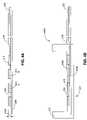
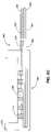
- FIG. 1is a flow diagram illustrating a method for fabricating a substrate in accordance with one embodiment of the present invention
- FIGS. 2A-2Jare schematic, top ( FIGS. 2A , 2 I- 2 J) and cross-sectional ( FIGS. 2B-2H ) views of portions of a substrate during successive stages of the method of FIG. 1 ;
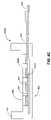
- FIGS. 3A-3Care schematic, cross-sectional ( FIGS. 3A-3B ) and top ( FIG. 3C ) views of portions of a substrate during successive stages of a method according to another embodiment of the invention
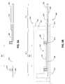
- FIGS. 4A-4Dare schematic, cross-sectional ( FIGS. 4A-4C ) and top ( FIG. 4D ) views of portions of a substrate during successive stages of a method according to yet another embodiment of the invention
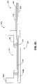
- FIGS. 5A-5Care schematic, cross-sectional views of portions of a substrate during successive stages of a method according to still another embodiment of the invention.
- FIGS. 6A-6Care schematic, cross-sectional views of portions of a substrate during successive stages of a method according to a further embodiment of the invention.
- FIGS. 7A-7Gare schematic, cross-sectional views of exemplary microelectronic assemblies using the substrates fabricated according to embodiments of the invention.
- FIG. 1depicts a flow diagram illustrating a method 100 for fabricating a flexible substrate for a microelectronic assembly in accordance with one embodiment of the present invention.
- the method 100includes processing steps performed during fabrication of a substrate for a microelectronic assembly. In some embodiments, these processing steps are performed in the depicted order. In alternate embodiments, at least two of these steps may be performed contemporaneously or in a different order. Sub-steps and auxiliary procedures (e.g., substrate transfers between processing reactors, substrate cleaning sub-steps, process control sub-steps, and the like) are well known in the art and, as such, herein are omitted. Cross-sectional views in the drawings below are taken along a line 1 - 1 (shown in FIGS. 2A and 2I only) of conductive plates of substrates being fabricated using embodiments of the method 100 .
- the method 100starts at step 102 and proceeds to step 104 .
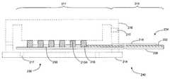
- the methoduses at least one conductive plate 200 for manufacturing electrical elements of a substrate being fabricated ( FIGS. 2A-2B ).
- the plate 200is fabricated principally from copper (Cu) and may have a width 202 in a range from about 5 to 50 mm, a length 204 in a range from about 10 to 500 mm, and a thickness 206 in a range from about 10 to 500 ⁇ m (e.g., 25-40 ⁇ m).
- the conductive plate 200may include a relatively thick top layer 200 A of an etchable material such as copper, a thin etch-stop 200 B, formed from another metal, such as nickel, and a bottom layer 200 C from an etchable material, such as copper.
- a flexible first dielectric film 208is deposited on a bottom surface 209 of the plate 200 , thereby forming a dielectric structure of the substrate being fabricated ( FIG. 2C ). Then, the plate 200 is patterned and etched to form contact elements, such as contact pins 210 (depicted as hatched areas) and unitary conductive traces 230 ( FIGS. 2D and 2I ).
- the pins 210may be formed by depositing a photoresist on the top layer 200 A only in the areas where the pins are to remain and etching away the top layer in other locations.
- the etch-stop layer 200 Bis then removed using a different etchant whereupon the bottom layer 200 C is selectively patterned with a photoresist and etched to leave the traces.
- Other processes for forming pins and traces on a dielectric layercan be used.
- the etch processuses the first dielectric film 208 as an etch stop layer to determine the duration of time for etching the plate 200 .
- the pins 210may be plated on the traces 230 , as well as both the pins 210 and traces 230 may be plated on the first dielectric film 208 or be formed using a combination of plating and etch processes.
- the pins 210are disposed in a first region 211
- the traces 230are disposed in both the first region 211 and an adjacent second region 213 of the dielectric film 208 .
- the traces 230are elongated strips extending from the first region 211 into the second region 213 , as shown in FIG. 2I below.
- first region 211the traces 230 are selectively connected to bases 210 B of the respective pins 210 .
- a length of first region 211is defined based on dimensions of microelectronic devices to be mounted on the substrate being fabricated, whereas a length of the region 213 is determined by a location of the substrate within an apparatus where such a substrate is used, as discussed below in reference to FIGS. 7A-7G .
- the pins 210are disposed at predetermined locations facilitating connection between the pins and terminals of the microelectronic device(s) to be mounted on the substrate. While the pins 210 are depicted herein as cylindrical columns, pins having different form factors have been contemplated and are within the scope of the present invention. For example, the pins 210 may have sidewalls 210 D that are sloped, as well as the sidewalls having rectangular or elliptical cross-sections. Reference is also made to U.S. Pat. No. 6,268,231 which is incorporated by reference in their entirety.
- Widths of tips 210 A and bases 210 B and heights 210 C of the pins 210are generally selected in a range from about 50 to 500 ⁇ m, 75 to 500 ⁇ m, and 10 to 500 ⁇ m, respectively. In one particular embodiment, the widths of the tips and bases and heights of the pins 210 were 100, 125, and 250 ⁇ m, respectively.
- Distances between the adjacent pinsgenerally correspond to the ones between terminals of the microelectronic devices to be mounted on the substrate and typically are in a range from 200 to 1000 ⁇ m, whereas widths of the traces 230 are typically selected in a range from about 5 to 100 ⁇ m (e.g., 20-40 ⁇ m). As such the width of the traces 230 may be substantially smaller than the widths of the bases of the pins 210 or the distances between the adjacent pins, thus facilitating high routing density in the region 211 and 213 of the substrate.
- each trace 230is connected to a base of at least one pin 210 or to at least one other trace, as illustratively depicted in FIG. 2I below.
- some tracesmay “float,” i.e., be electrically disconnected from pins and other traces of the substrate.
- one or more pins 210may remain unconnected to the traces 230 , although typically most or all of the pins are connected to the traces.
- the pins 210 and traces 230form an electrical circuit of the substrate.
- the tracesare further provided in the second region 213 with contacts 232 (e.g., etched contacts).
- the contacts 232are used to provide electrical connectivity between the substrate being fabricated and external circuits.
- pins 210 , contacts 232 , or traces 230may be provided with an optional coating (not shown), for example, gold (Au) coating, to enhance their conductivity, connectivity, and resistance to corrosion.
- Augold
- a flexible second dielectric film 218is formed in the region 213 over the traces 230 , with the exception for the contacts 232 ( FIG. 2E ).
- the films 208 and 218are formed from the same material (for example, polyimide and the like) and bonded together (e.g., molded or otherwise thermally, mechanically, or chemically processed) to encapsulate the traces 230 .
- the traces 230 and films 208 , 218form a flexible portion 234 of the substrate being fabricated.
- a dielectric enclosure 220is fabricated from a first dielectric encapsulant in the region 211 using a molding process, a curing process, or a combination thereof ( FIGS. 2F-2J ).
- the enclosure 220reinforces the dielectric structure 208 in the first region 211 so that the first region is more rigid than the second region 213 .
- the circuit elements of the substratesuch as pins 210 and traces 230 , and the underlying portion of the first dielectric film 208 are disposed between a press plate 214 (shown using broken lines) and a counter element 216 (shown using phantom lines) of a molding tool ( FIG. 2F ).
- the counter element 216is abutted against the tips 210 A of the pins 210 and a flowable molding composition is injected or otherwise introduced into the space between the press plate 214 and counter element 216 .
- a flowable molding compositionis injected or otherwise introduced into the space between the press plate 214 and counter element 216 .
- Such molding processforms the enclosure 220 ( FIG. 2G ) having a bottom surface 226 coplanar with the tips of the pins 210 and embedding, in the region 211 , the traces 230 and the dielectric film 208 .
- the compositionmay be essentially any material which will cure to a solid state and form a dielectric.
- compositions which cure by chemical reaction to form a polymeric dielectricsuch as epoxies, polyimides, or liquid crystal polymers may be used.
- the flowable compositionmay be a thermoplastic at an elevated temperature, which, by cooling, can be cured to a solid state.
- the enclosure 220after molding or curing, forms binding interfaces with the features (i.e., pins 210 and traces 230 ) of the substrate 240 .
- the compositionmay further include one or more additives influencing properties of the enclosure 220 .
- additivesmay include particulate materials such as silica or other inorganic dielectrics, or fibrous reinforcements such as short glass fibers.
- the molding compositionis injected through at least one opening, or gate, 217 in the counter element 216 and/or the press plate 214 , whereas the remaining openings 217 are used as an escape passage for the trapped air or excess material of the molding composition.
- the molded enclosure 220comprises a top portion 220 A encapsulating the pins 210 and traces 230 and a bottom portion 220 B encapsulating the first flexible dielectric film 208 .
- the enclosure 220may also be molded over a portion 218 A of the second dielectric film 218 ( FIG. 2H ).
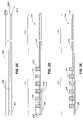
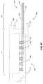
- FIG. 2Idepicts a top view of the substrate 240 .
- the traces 230are shown in FIG. 2I using thick solid lines. However, the traces 230 are embedded, in the region 211 , in the enclosure 220 and, in the region 213 , disposed beneath the second dielectric film 218 .
- the tips of the pins 210are free from the molding composition.
- a thin layer (not shown) of the molding compositionmay overlie the tips of some or all of the pins 210 . If this occurs, such a layer can be removed by exposing the surface 226 to a brief plasma etching or ashing process which attacks and remove the layer.
- a width of the dielectric film 208 in the region 211may optionally be reduced, as illustratively depicted in FIG. 2I using a broken line 215 . Exposing pins 210 and 230 facilitates a better connection.
- the pins 210will be “exposed at” the surface after the completion of the molding step.
- a metallic featurecan be considered “exposed at” a surface of a dielectric layer if the metallic feature is accessible to a contact or bonding material applied to such surface.
- a metallic feature which projects from the surface of the dielectric, such as pins 210 or traces 230 , or which is flush with the surface of the dielectricis also “exposed at” the surface.
- the top portion 220 A of the enclosureincludes a peripheral wall 212 projecting from the dielectric structure and surrounding the region 211 .
- the wall 212may be used to support a lid covering the enclosure 220 and/or comprising components facilitating operability of microelectronic devices mounted on the substrate 240 .
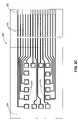
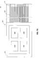
- the portions 236 of several substrates 240may be molded simultaneously as illustratively shown in FIG. 2J , where a larger frame 242 incorporates a plurality of individual press plates 214 .
- the frame 242illustratively includes sprocket holes 244 and a peripheral wall 246 .
- the counter elements 216 of the molding toolare extended over the plate 242 .
- the molding compositionis introduced into the spaces between the component press plates 214 and counter elements 216 through individual gates 217 flowably coupled to a runner system of the molding tool.
- the method 100ends.
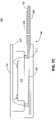
- a substrate 340comprises a flat enclosure 320 ( FIGS. 3A-3C ).
- a process of molding the enclosure 320is illustrated in FIG. 3A .
- the tips 210 A of the pins 210are in a contact with an inner surface 302 of a counter plate 316 .
- the counter plate 316forms a molding cavity for molding the enclosure 320 .
- An upper surface 326 of the molded enclosure 320is coplanar with the tips of the pins 210 ( FIG. 3B ). In FIG.
- FIG. 3Cdepicting a top view of the substrate 340 , the traces 230 are shown terminated with optional contact areas 304 , which totally (as shown) or at least partially surround bases of the respective pins (traces 230 and areas 304 are shown using thick solid lines).
- Substrate 440 A and 440 Bcomprise contact elements in a form of contact pads 410 ( FIGS. 4A-4D ).
- the pads 410have larger tips and larger bases than the ones of the pins 210 , thereby allowing for greater manufacturing tolerances during mounting of microelectronic devices onto such substrates ( FIG. 4A ).
- widths of the tips 410 A and bases 410 B of the pads 410are generally selected in a range from 500 to 1000 ⁇ m, whereas a height 410 C of the pads is typically in a range from 10 to 500 ⁇ m.
- the height 410 C of the pads 410may be greater than the height of the traces 230 (as illustratively shown in FIGS. 4A-4C ), as well as equal or smaller (not shown) than the height of the traces 230 .
- Such pads 410may be formed (for example, etched or plated) using the same processes as discussed above in reference to fabrication of the pins 210 .
- an upper surface 426 A of a molded enclosure 420 Ais coplanar with the tips 410 A of the pads 410 of the substrate 440 A.
- an upper surface 426 B of the enclosure 420 Bis disposed above the tips 410 A of the pads 410 , and the pads 410 are accessible through openings 404 in the surface 426 B.
- Such openings 404may be formed, for example, during the molding process that uses a molding tool where a counter plate includes columns matching the openings 404 .
- the openings 404may also be etched or mechanically machined in the enclosure 420 .
- FIG. 4Ddepicts a top view of the substrate 440 A or 440 B (traces 230 are shown using thick solid lines).
- the contact elementsmay include some contact pads and some contact pins.
- a substrate 540comprises a dielectric enclosure 520 having a recess 504 disposed in region 501 of the enclosure ( FIGS. 5A-5C ).
- the recessmay be adapted for receiving microelectronic devices mounted on the substrate 540 .
- the contact elements(illustratively, pins 210 ) are horizontally offset from the recess 502 ( FIG. 5A ).
- the traces 230may also be offset from the recess, as well as the recess may be extended from an upper portion 520 A into a bottom portion 520 B of the enclosure.
- the recess 504may be fabricated, for example, during the molding process using a counter plate 516 provided with a step 502 that matches the recess to be formed, as well as the recess may be etched or mechanically machined in the enclosure 520 ( FIG. 5B-5C ).
- a substrate 640comprises a conductive layer 602 and a third dielectric layer 604 , which are consecutively formed on the first dielectric layer 208 ( FIGS. 6A-6C ).
- the layer 602is provided with an electrical contact 606 for connecting to a circuit external to the substrate 640 ( FIG. 6B ).
- the enclosure 220encapsulates the layers 602 and 604 ( FIG. 6C ).
- the conductive layer 602may be used as a shield protecting the circuits of the substrate 640 from electromagnetic interference (EMI) caused by external circuits.
- EMIelectromagnetic interference
- Substrates fabricated according to yet further embodiments of the method of FIG. 1may comprise various combinations of the features discussed above in reference to the substrates 240 , 340 , 440 A- 440 B, 540 , and 640 .
- the substrates 240 , 340 , 440 A- 440 B, and 640may include recesses, like those included in the substrate 540 .
- the inventive substratesadvantageously overcome many deficiencies of the prior art.
- FIGS. 7A-7Gdepict exemplary microelectronic assemblies 701 - 707 using the substrate fabricated according to embodiments of the present invention.
- Microelectronic elements, or devicesare electrically connected to contact elements and may be mounted on the substrates using a ball bonding technique (also known in the art as a flip-chip technique) and/or a wire bonding technique.
- the devices mounted on the substratesare collectively denoted herein using the same reference numeral 720 , except that, in FIG. 7G , the suffixes “A”-“D” have been added to differentiate between the individual devices.
- the devices 720may include various electronic or opto-electronic sensor arrays, micro-electromechanical systems (MEMS), and other microelectronic chips used in digital cameras, cellular phones, laptop computers, finger print readers and the like products or component sub-assemblies of such or other products.
- MEMSmicro-electromechanical systems
- the devices 720may additionally or optionally be affixed to the respective enclosures using, for example, an adhesive compound, be at least partially encapsulated within the enclosures using a protective compound, or the enclosures and the mounted devices may be at least partially encapsulated using the protective compound.
- an adhesive compoundbe at least partially encapsulated within the enclosures using a protective compound
- the enclosures and the mounted devicesmay be at least partially encapsulated using the protective compound.
- Such adhesive and protective compounds and methods of their applicationare known in the art and therefore are not shown in the FIGS. 7A-7G .
- FIGS. 7A-7Gdepict exemplary microelectronic assemblies, or units, 701 - 703 each comprising the substrate 240 having a plurality of contact pins 210 adapted for connecting to corresponding terminals of the devices 720 using a flip-chip technique (i.e., solder-bonded to the respective terminals) as depicted in FIGS. 7A-7B or using a wire bonding technique ( FIG. 7C ).
- FIGS. 7D and 7Edepict the assemblies 704 and 705 comprising the substrates 440 A ( FIG. 7D) and 440B ( FIG. 7B ), respectively, whereas the assembly 706 comprising the substrate 340 is shown in FIG. 7F .
- FIG. 7Gseveral devices 720 (illustratively, devices 720 A- 720 D) are mounted on the same substrate 240 .
- the enclosure 220is provided with a lid 720 supporting a transparent window 710 to facilitate operability of the device 720 containing an array of opto-electronic cells.
- the enclosure 220is shown with an attached optical assembly 716 including a housing 712 and lenses 710 , 714 .
- the assembly 716may facilitate operability of the device 720 comprising, for example, a finger print sensor array or optical MEMS.
- a cover 722may, for example, seal or mechanically protect the devices 720 .
Landscapes
- Engineering & Computer Science (AREA)
- Microelectronics & Electronic Packaging (AREA)
- Computer Hardware Design (AREA)
- Physics & Mathematics (AREA)
- Condensed Matter Physics & Semiconductors (AREA)
- General Physics & Mathematics (AREA)
- Power Engineering (AREA)
- Structure Of Printed Boards (AREA)
- Combinations Of Printed Boards (AREA)
Abstract
Description
Claims (23)
Priority Applications (2)
| Application Number | Priority Date | Filing Date | Title |
|---|---|---|---|
| US11/606,771US7659617B2 (en) | 2006-11-30 | 2006-11-30 | Substrate for a flexible microelectronic assembly and a method of fabricating thereof |
| PCT/US2007/024589WO2008066894A2 (en) | 2006-11-30 | 2007-11-28 | Substrate for a flexible microelectronic assembly |
Applications Claiming Priority (1)
| Application Number | Priority Date | Filing Date | Title |
|---|---|---|---|
| US11/606,771US7659617B2 (en) | 2006-11-30 | 2006-11-30 | Substrate for a flexible microelectronic assembly and a method of fabricating thereof |
Publications (2)
| Publication Number | Publication Date |
|---|---|
| US20080128886A1 US20080128886A1 (en) | 2008-06-05 |
| US7659617B2true US7659617B2 (en) | 2010-02-09 |
Family
ID=39268190
Family Applications (1)
| Application Number | Title | Priority Date | Filing Date |
|---|---|---|---|
| US11/606,771Active2028-02-02US7659617B2 (en) | 2006-11-30 | 2006-11-30 | Substrate for a flexible microelectronic assembly and a method of fabricating thereof |
Country Status (2)
| Country | Link |
|---|---|
| US (1) | US7659617B2 (en) |
| WO (1) | WO2008066894A2 (en) |
Cited By (28)
| Publication number | Priority date | Publication date | Assignee | Title |
|---|---|---|---|---|
| US20100263918A1 (en)* | 2010-06-29 | 2010-10-21 | Layout Method And Circuit B | Layout method and circuit board |
| US20110285890A1 (en)* | 2010-05-20 | 2011-11-24 | Samsung Electronics Co., Ltd. | Camera module |
| US9490222B1 (en) | 2015-10-12 | 2016-11-08 | Invensas Corporation | Wire bond wires for interference shielding |
| US9735084B2 (en) | 2014-12-11 | 2017-08-15 | Invensas Corporation | Bond via array for thermal conductivity |
| US9761554B2 (en) | 2015-05-07 | 2017-09-12 | Invensas Corporation | Ball bonding metal wire bond wires to metal pads |
| US9842745B2 (en) | 2012-02-17 | 2017-12-12 | Invensas Corporation | Heat spreading substrate with embedded interconnects |
| US9852969B2 (en) | 2013-11-22 | 2017-12-26 | Invensas Corporation | Die stacks with one or more bond via arrays of wire bond wires and with one or more arrays of bump interconnects |
| US9888579B2 (en) | 2015-03-05 | 2018-02-06 | Invensas Corporation | Pressing of wire bond wire tips to provide bent-over tips |
| US9911718B2 (en) | 2015-11-17 | 2018-03-06 | Invensas Corporation | ‘RDL-First’ packaged microelectronic device for a package-on-package device |
| US9935075B2 (en) | 2016-07-29 | 2018-04-03 | Invensas Corporation | Wire bonding method and apparatus for electromagnetic interference shielding |
| US9953914B2 (en) | 2012-05-22 | 2018-04-24 | Invensas Corporation | Substrate-less stackable package with wire-bond interconnect |
| US9984992B2 (en) | 2015-12-30 | 2018-05-29 | Invensas Corporation | Embedded wire bond wires for vertical integration with separate surface mount and wire bond mounting surfaces |
| US10008477B2 (en) | 2013-09-16 | 2018-06-26 | Invensas Corporation | Microelectronic element with bond elements to encapsulation surface |
| US10008469B2 (en) | 2015-04-30 | 2018-06-26 | Invensas Corporation | Wafer-level packaging using wire bond wires in place of a redistribution layer |
| US10026717B2 (en) | 2013-11-22 | 2018-07-17 | Invensas Corporation | Multiple bond via arrays of different wire heights on a same substrate |
| US10062661B2 (en) | 2011-05-03 | 2018-08-28 | Tessera, Inc. | Package-on-package assembly with wire bonds to encapsulation surface |
| US10128216B2 (en) | 2010-07-19 | 2018-11-13 | Tessera, Inc. | Stackable molded microelectronic packages |
| US10181457B2 (en) | 2015-10-26 | 2019-01-15 | Invensas Corporation | Microelectronic package for wafer-level chip scale packaging with fan-out |
| US10299368B2 (en) | 2016-12-21 | 2019-05-21 | Invensas Corporation | Surface integrated waveguides and circuit structures therefor |
| US10297582B2 (en) | 2012-08-03 | 2019-05-21 | Invensas Corporation | BVA interposer |
| US10332854B2 (en) | 2015-10-23 | 2019-06-25 | Invensas Corporation | Anchoring structure of fine pitch bva |
| US10381326B2 (en) | 2014-05-28 | 2019-08-13 | Invensas Corporation | Structure and method for integrated circuits packaging with increased density |
| US10460958B2 (en) | 2013-08-07 | 2019-10-29 | Invensas Corporation | Method of manufacturing embedded packaging with preformed vias |
| US10490528B2 (en) | 2015-10-12 | 2019-11-26 | Invensas Corporation | Embedded wire bond wires |
| US10529636B2 (en) | 2014-01-17 | 2020-01-07 | Invensas Corporation | Fine pitch BVA using reconstituted wafer with area array accessible for testing |
| US10756049B2 (en) | 2011-10-17 | 2020-08-25 | Invensas Corporation | Package-on-package assembly with wire bond vias |
| US10973142B2 (en) | 2017-05-18 | 2021-04-06 | Covidien Lp | Hermetically sealed printed circuit boards |
| US20220182516A1 (en)* | 2019-08-22 | 2022-06-09 | Samsung Electronics Co., Ltd. | Camera module including printed circuit board, and electronic device comprising same |
Families Citing this family (12)
| Publication number | Priority date | Publication date | Assignee | Title |
|---|---|---|---|---|
| US7759782B2 (en)* | 2006-04-07 | 2010-07-20 | Tessera, Inc. | Substrate for a microelectronic package and method of fabricating thereof |
| EP2252469B1 (en)* | 2008-03-11 | 2012-10-24 | Rolic Ltd. | Optical biometric security element |
| FI122216B (en)* | 2009-01-05 | 2011-10-14 | Imbera Electronics Oy | Rigid-flex module |
| TWM377018U (en)* | 2009-09-09 | 2010-03-21 | Azurewave Technologies Inc | Flip chip type image capturing module |
| DE102010020190A1 (en)* | 2010-05-11 | 2011-11-17 | Sendsor Gmbh | Method for manufacturing electrical sensing unit for sensing moisture, involves forming electrical sensor structure in metal layer of sensor portion by partial removal of metal film from sensor portion |
| DE102011109006A1 (en)* | 2011-07-29 | 2013-01-31 | Epcos Ag | Housing for a semiconductor chip and semiconductor chip with a housing |
| ITTO20120827A1 (en)* | 2012-09-24 | 2014-03-25 | St Microelectronics Srl | INSULATION AT SLICE LEVEL OF AN INTEGRATED MEMS DEVICE AND ITS MANUFACTURING PROCEDURE |
| US9646917B2 (en) | 2014-05-29 | 2017-05-09 | Invensas Corporation | Low CTE component with wire bond interconnects |
| KR20180032985A (en)* | 2016-09-23 | 2018-04-02 | 삼성전자주식회사 | Integrated circuit package and method of manufacturing the same and wearable device including integrated circuit package |
| CN108726470B (en)* | 2017-04-21 | 2020-02-21 | 华为技术有限公司 | MEMS chip and electrical packaging method thereof |
| US10588231B2 (en)* | 2017-05-18 | 2020-03-10 | Covidien Lp | Hermetically sealed printed circuit boards |
| US10667408B2 (en) | 2017-05-18 | 2020-05-26 | Covidien Lp | Fully encapsulated electronics and printed circuit boards |
Citations (8)
| Publication number | Priority date | Publication date | Assignee | Title |
|---|---|---|---|---|
| GB2236062A (en) | 1989-05-10 | 1991-03-27 | Peter Moran | Integrated circuit package |
| DE4428158A1 (en) | 1993-08-13 | 1995-02-16 | Motorola Inc | Optoelectronic interface module and method for the production thereof |
| US6268231B1 (en) | 1996-04-08 | 2001-07-31 | Eastman Kodak Company | Low cost CCD packaging |
| US6320128B1 (en) | 2000-05-25 | 2001-11-20 | Visteon Global Technology, Inc. | Environmentally-sealed electronic assembly and method of making same |
| US20020006696A1 (en)* | 2000-06-08 | 2002-01-17 | Salman Akram | Protective structures for bond wires, methods for forming same, and test apparatus including such structures |
| US20030233134A1 (en) | 2002-04-11 | 2003-12-18 | Greenberg Robert J. | Biocompatible bonding method and electronics package suitable for implantation |
| US20040042183A1 (en) | 2002-09-04 | 2004-03-04 | Alcaria Vicente D. | Flex circuit package |
| US20050174469A1 (en) | 2004-02-11 | 2005-08-11 | Min-Kyo Cho | Wiring substrate, solid-state imaging apparatus using the same, and manufacturing method thereof |
- 2006
- 2006-11-30USUS11/606,771patent/US7659617B2/enactiveActive
- 2007
- 2007-11-28WOPCT/US2007/024589patent/WO2008066894A2/enactiveApplication Filing
Patent Citations (8)
| Publication number | Priority date | Publication date | Assignee | Title |
|---|---|---|---|---|
| GB2236062A (en) | 1989-05-10 | 1991-03-27 | Peter Moran | Integrated circuit package |
| DE4428158A1 (en) | 1993-08-13 | 1995-02-16 | Motorola Inc | Optoelectronic interface module and method for the production thereof |
| US6268231B1 (en) | 1996-04-08 | 2001-07-31 | Eastman Kodak Company | Low cost CCD packaging |
| US6320128B1 (en) | 2000-05-25 | 2001-11-20 | Visteon Global Technology, Inc. | Environmentally-sealed electronic assembly and method of making same |
| US20020006696A1 (en)* | 2000-06-08 | 2002-01-17 | Salman Akram | Protective structures for bond wires, methods for forming same, and test apparatus including such structures |
| US20030233134A1 (en) | 2002-04-11 | 2003-12-18 | Greenberg Robert J. | Biocompatible bonding method and electronics package suitable for implantation |
| US20040042183A1 (en) | 2002-09-04 | 2004-03-04 | Alcaria Vicente D. | Flex circuit package |
| US20050174469A1 (en) | 2004-02-11 | 2005-08-11 | Min-Kyo Cho | Wiring substrate, solid-state imaging apparatus using the same, and manufacturing method thereof |
Non-Patent Citations (1)
| Title |
|---|
| International Search Report, PCT/US2007/24589, Written opinion dated May 14, 2008. |
Cited By (49)
| Publication number | Priority date | Publication date | Assignee | Title |
|---|---|---|---|---|
| US20110285890A1 (en)* | 2010-05-20 | 2011-11-24 | Samsung Electronics Co., Ltd. | Camera module |
| US20100263918A1 (en)* | 2010-06-29 | 2010-10-21 | Layout Method And Circuit B | Layout method and circuit board |
| US10128216B2 (en) | 2010-07-19 | 2018-11-13 | Tessera, Inc. | Stackable molded microelectronic packages |
| US11424211B2 (en) | 2011-05-03 | 2022-08-23 | Tessera Llc | Package-on-package assembly with wire bonds to encapsulation surface |
| US10593643B2 (en) | 2011-05-03 | 2020-03-17 | Tessera, Inc. | Package-on-package assembly with wire bonds to encapsulation surface |
| US10062661B2 (en) | 2011-05-03 | 2018-08-28 | Tessera, Inc. | Package-on-package assembly with wire bonds to encapsulation surface |
| US11189595B2 (en) | 2011-10-17 | 2021-11-30 | Invensas Corporation | Package-on-package assembly with wire bond vias |
| US10756049B2 (en) | 2011-10-17 | 2020-08-25 | Invensas Corporation | Package-on-package assembly with wire bond vias |
| US11735563B2 (en) | 2011-10-17 | 2023-08-22 | Invensas Llc | Package-on-package assembly with wire bond vias |
| US9842745B2 (en) | 2012-02-17 | 2017-12-12 | Invensas Corporation | Heat spreading substrate with embedded interconnects |
| US10510659B2 (en) | 2012-05-22 | 2019-12-17 | Invensas Corporation | Substrate-less stackable package with wire-bond interconnect |
| US10170412B2 (en) | 2012-05-22 | 2019-01-01 | Invensas Corporation | Substrate-less stackable package with wire-bond interconnect |
| US9953914B2 (en) | 2012-05-22 | 2018-04-24 | Invensas Corporation | Substrate-less stackable package with wire-bond interconnect |
| US10297582B2 (en) | 2012-08-03 | 2019-05-21 | Invensas Corporation | BVA interposer |
| US10460958B2 (en) | 2013-08-07 | 2019-10-29 | Invensas Corporation | Method of manufacturing embedded packaging with preformed vias |
| US10008477B2 (en) | 2013-09-16 | 2018-06-26 | Invensas Corporation | Microelectronic element with bond elements to encapsulation surface |
| US10026717B2 (en) | 2013-11-22 | 2018-07-17 | Invensas Corporation | Multiple bond via arrays of different wire heights on a same substrate |
| USRE49987E1 (en) | 2013-11-22 | 2024-05-28 | Invensas Llc | Multiple plated via arrays of different wire heights on a same substrate |
| US10629567B2 (en) | 2013-11-22 | 2020-04-21 | Invensas Corporation | Multiple plated via arrays of different wire heights on same substrate |
| US10290613B2 (en) | 2013-11-22 | 2019-05-14 | Invensas Corporation | Multiple bond via arrays of different wire heights on a same substrate |
| US9852969B2 (en) | 2013-11-22 | 2017-12-26 | Invensas Corporation | Die stacks with one or more bond via arrays of wire bond wires and with one or more arrays of bump interconnects |
| US11990382B2 (en) | 2014-01-17 | 2024-05-21 | Adeia Semiconductor Technologies Llc | Fine pitch BVA using reconstituted wafer with area array accessible for testing |
| US11404338B2 (en) | 2014-01-17 | 2022-08-02 | Invensas Corporation | Fine pitch bva using reconstituted wafer with area array accessible for testing |
| US10529636B2 (en) | 2014-01-17 | 2020-01-07 | Invensas Corporation | Fine pitch BVA using reconstituted wafer with area array accessible for testing |
| US10381326B2 (en) | 2014-05-28 | 2019-08-13 | Invensas Corporation | Structure and method for integrated circuits packaging with increased density |
| US9735084B2 (en) | 2014-12-11 | 2017-08-15 | Invensas Corporation | Bond via array for thermal conductivity |
| US9888579B2 (en) | 2015-03-05 | 2018-02-06 | Invensas Corporation | Pressing of wire bond wire tips to provide bent-over tips |
| US10806036B2 (en) | 2015-03-05 | 2020-10-13 | Invensas Corporation | Pressing of wire bond wire tips to provide bent-over tips |
| US10008469B2 (en) | 2015-04-30 | 2018-06-26 | Invensas Corporation | Wafer-level packaging using wire bond wires in place of a redistribution layer |
| US9761554B2 (en) | 2015-05-07 | 2017-09-12 | Invensas Corporation | Ball bonding metal wire bond wires to metal pads |
| US10559537B2 (en) | 2015-10-12 | 2020-02-11 | Invensas Corporation | Wire bond wires for interference shielding |
| US10115678B2 (en) | 2015-10-12 | 2018-10-30 | Invensas Corporation | Wire bond wires for interference shielding |
| US9812402B2 (en) | 2015-10-12 | 2017-11-07 | Invensas Corporation | Wire bond wires for interference shielding |
| US10490528B2 (en) | 2015-10-12 | 2019-11-26 | Invensas Corporation | Embedded wire bond wires |
| US9490222B1 (en) | 2015-10-12 | 2016-11-08 | Invensas Corporation | Wire bond wires for interference shielding |
| US11462483B2 (en) | 2015-10-12 | 2022-10-04 | Invensas Llc | Wire bond wires for interference shielding |
| US10332854B2 (en) | 2015-10-23 | 2019-06-25 | Invensas Corporation | Anchoring structure of fine pitch bva |
| US10181457B2 (en) | 2015-10-26 | 2019-01-15 | Invensas Corporation | Microelectronic package for wafer-level chip scale packaging with fan-out |
| US9911718B2 (en) | 2015-11-17 | 2018-03-06 | Invensas Corporation | ‘RDL-First’ packaged microelectronic device for a package-on-package device |
| US10043779B2 (en) | 2015-11-17 | 2018-08-07 | Invensas Corporation | Packaged microelectronic device for a package-on-package device |
| US9984992B2 (en) | 2015-12-30 | 2018-05-29 | Invensas Corporation | Embedded wire bond wires for vertical integration with separate surface mount and wire bond mounting surfaces |
| US10325877B2 (en) | 2015-12-30 | 2019-06-18 | Invensas Corporation | Embedded wire bond wires for vertical integration with separate surface mount and wire bond mounting surfaces |
| US9935075B2 (en) | 2016-07-29 | 2018-04-03 | Invensas Corporation | Wire bonding method and apparatus for electromagnetic interference shielding |
| US10658302B2 (en) | 2016-07-29 | 2020-05-19 | Invensas Corporation | Wire bonding method and apparatus for electromagnetic interference shielding |
| US10299368B2 (en) | 2016-12-21 | 2019-05-21 | Invensas Corporation | Surface integrated waveguides and circuit structures therefor |
| US11304324B2 (en) | 2017-05-18 | 2022-04-12 | Covidien Lp | Hermetically sealed printed circuit boards |
| US10973142B2 (en) | 2017-05-18 | 2021-04-06 | Covidien Lp | Hermetically sealed printed circuit boards |
| US20220182516A1 (en)* | 2019-08-22 | 2022-06-09 | Samsung Electronics Co., Ltd. | Camera module including printed circuit board, and electronic device comprising same |
| US12096105B2 (en)* | 2019-08-22 | 2024-09-17 | Samsung Electronics Co., Ltd | Camera module including printed circuit board, and electronic device comprising same |
Also Published As
| Publication number | Publication date |
|---|---|
| US20080128886A1 (en) | 2008-06-05 |
| WO2008066894A3 (en) | 2008-08-14 |
| WO2008066894A2 (en) | 2008-06-05 |
Similar Documents
| Publication | Publication Date | Title |
|---|---|---|
| US7659617B2 (en) | Substrate for a flexible microelectronic assembly and a method of fabricating thereof | |
| US7141886B2 (en) | Air pocket resistant semiconductor package | |
| KR100918745B1 (en) | A semiconductor device and method of manufacturing the same | |
| KR101075241B1 (en) | Microelectronic package with terminals in dielectric member | |
| US7061077B2 (en) | Substrate based unmolded package including lead frame structure and semiconductor die | |
| CN100382260C (en) | Manufacturing method of semiconductor package | |
| US5989939A (en) | Process of manufacturing compliant wirebond packages | |
| US20100213599A1 (en) | Semiconductor device and manufacturing method thereof | |
| US6731010B2 (en) | Resin sealed stacked semiconductor packages with flat surfaces | |
| TWI483356B (en) | Molded ultra-thin semiconductor die package, system using the same, and method of manufacturing the same | |
| CN101231709A (en) | Structure of memory card and method thereof | |
| US7911068B2 (en) | Component and method for producing a component | |
| EP1984949A2 (en) | A sip module with a single sided lid | |
| KR20090050969A (en) | Drop-Mold Matching Material Used as Encapsulant for Integrated Circuit Package Systems | |
| CN101238576A (en) | Rigid wave pattern design on chip carrier substrates and printed circuit boards for semiconductor and electronic subsystem packaging | |
| KR20090122277A (en) | Microelectronic Workpieces and Microelectronic Device Manufacturing Methods Using the Workpieces | |
| US6936922B1 (en) | Semiconductor package structure reducing warpage and manufacturing method thereof | |
| US8293572B2 (en) | Injection molding system and method of chip package | |
| US7344915B2 (en) | Method for manufacturing a semiconductor package with a laminated chip cavity | |
| WO2019007082A1 (en) | Chip encapsulation method | |
| US11655143B2 (en) | Semiconductor component and method for producing same | |
| CN101796634B (en) | Subassembly that includes a power semiconductor die and a heat sink having an exposed surface portion thereof | |
| KR100850213B1 (en) | Semiconductor package having molded balls and manufacturing method thereof | |
| US8274125B2 (en) | Semiconductor device and semiconductor device manufacturing method | |
| WO2019103681A1 (en) | Fingerprint sensor package with desired component outline and method for manufacturing thereof |
Legal Events
| Date | Code | Title | Description |
|---|---|---|---|
| AS | Assignment | Owner name:TESSERA, INC., CALIFORNIA Free format text:ASSIGNMENT OF ASSIGNORS INTEREST;ASSIGNORS:KANG, TECK-GYU;PARK, JAE M.;KUBOTA, YOICHI;REEL/FRAME:020173/0750;SIGNING DATES FROM 20061215 TO 20070817 Owner name:TESSERA, INC.,CALIFORNIA Free format text:ASSIGNMENT OF ASSIGNORS INTEREST;ASSIGNORS:KANG, TECK-GYU;PARK, JAE M.;KUBOTA, YOICHI;SIGNING DATES FROM 20061215 TO 20070817;REEL/FRAME:020173/0750 | |
| STCF | Information on status: patent grant | Free format text:PATENTED CASE | |
| CC | Certificate of correction | ||
| FPAY | Fee payment | Year of fee payment:4 | |
| AS | Assignment | Owner name:ROYAL BANK OF CANADA, AS COLLATERAL AGENT, CANADA Free format text:SECURITY INTEREST;ASSIGNORS:INVENSAS CORPORATION;TESSERA, INC.;TESSERA ADVANCED TECHNOLOGIES, INC.;AND OTHERS;REEL/FRAME:040797/0001 Effective date:20161201 | |
| FPAY | Fee payment | Year of fee payment:8 | |
| AS | Assignment | Owner name:BANK OF AMERICA, N.A., NORTH CAROLINA Free format text:SECURITY INTEREST;ASSIGNORS:ROVI SOLUTIONS CORPORATION;ROVI TECHNOLOGIES CORPORATION;ROVI GUIDES, INC.;AND OTHERS;REEL/FRAME:053468/0001 Effective date:20200601 | |
| AS | Assignment | Owner name:DTS LLC, CALIFORNIA Free format text:RELEASE BY SECURED PARTY;ASSIGNOR:ROYAL BANK OF CANADA;REEL/FRAME:052920/0001 Effective date:20200601 Owner name:INVENSAS BONDING TECHNOLOGIES, INC. (F/K/A ZIPTRONIX, INC.), CALIFORNIA Free format text:RELEASE BY SECURED PARTY;ASSIGNOR:ROYAL BANK OF CANADA;REEL/FRAME:052920/0001 Effective date:20200601 Owner name:PHORUS, INC., CALIFORNIA Free format text:RELEASE BY SECURED PARTY;ASSIGNOR:ROYAL BANK OF CANADA;REEL/FRAME:052920/0001 Effective date:20200601 Owner name:FOTONATION CORPORATION (F/K/A DIGITALOPTICS CORPORATION AND F/K/A DIGITALOPTICS CORPORATION MEMS), CALIFORNIA Free format text:RELEASE BY SECURED PARTY;ASSIGNOR:ROYAL BANK OF CANADA;REEL/FRAME:052920/0001 Effective date:20200601 Owner name:DTS, INC., CALIFORNIA Free format text:RELEASE BY SECURED PARTY;ASSIGNOR:ROYAL BANK OF CANADA;REEL/FRAME:052920/0001 Effective date:20200601 Owner name:IBIQUITY DIGITAL CORPORATION, MARYLAND Free format text:RELEASE BY SECURED PARTY;ASSIGNOR:ROYAL BANK OF CANADA;REEL/FRAME:052920/0001 Effective date:20200601 Owner name:INVENSAS CORPORATION, CALIFORNIA Free format text:RELEASE BY SECURED PARTY;ASSIGNOR:ROYAL BANK OF CANADA;REEL/FRAME:052920/0001 Effective date:20200601 Owner name:TESSERA ADVANCED TECHNOLOGIES, INC, CALIFORNIA Free format text:RELEASE BY SECURED PARTY;ASSIGNOR:ROYAL BANK OF CANADA;REEL/FRAME:052920/0001 Effective date:20200601 Owner name:TESSERA, INC., CALIFORNIA Free format text:RELEASE BY SECURED PARTY;ASSIGNOR:ROYAL BANK OF CANADA;REEL/FRAME:052920/0001 Effective date:20200601 | |
| MAFP | Maintenance fee payment | Free format text:PAYMENT OF MAINTENANCE FEE, 12TH YEAR, LARGE ENTITY (ORIGINAL EVENT CODE: M1553); ENTITY STATUS OF PATENT OWNER: LARGE ENTITY Year of fee payment:12 |