US7659536B2 - High performance hyperspectral detectors using photon controlling cavities - Google Patents
High performance hyperspectral detectors using photon controlling cavitiesDownload PDFInfo
- Publication number
- US7659536B2 US7659536B2US11/225,006US22500605AUS7659536B2US 7659536 B2US7659536 B2US 7659536B2US 22500605 AUS22500605 AUS 22500605AUS 7659536 B2US7659536 B2US 7659536B2
- Authority
- US
- United States
- Prior art keywords
- photodetector
- layer
- quantum dot
- photonic crystal
- resonant cavity
- Prior art date
- Legal status (The legal status is an assumption and is not a legal conclusion. Google has not performed a legal analysis and makes no representation as to the accuracy of the status listed.)
- Expired - Fee Related, expires
Links
- 239000004038photonic crystalSubstances0.000claimsabstractdescription49
- 239000002096quantum dotSubstances0.000claimsdescription42
- 229910001218Gallium arsenideInorganic materials0.000claimsdescription20
- 230000007547defectEffects0.000claimsdescription20
- 230000004888barrier functionEffects0.000claimsdescription18
- 229910000530Gallium indium arsenideInorganic materials0.000claimsdescription10
- 239000004065semiconductorSubstances0.000claimsdescription8
- RPQDHPTXJYYUPQ-UHFFFAOYSA-Nindium arsenideChemical compound[In]#[As]RPQDHPTXJYYUPQ-UHFFFAOYSA-N0.000claimsdescription7
- 230000003595spectral effectEffects0.000claimsdescription7
- 229910000673Indium arsenideInorganic materials0.000claimsdescription6
- 229910045601alloyInorganic materials0.000claimsdescription6
- 239000000956alloySubstances0.000claimsdescription6
- 239000000969carrierSubstances0.000claimsdescription3
- 150000001875compoundsChemical class0.000claimsdescription2
- 230000004044responseEffects0.000abstractdescription5
- 239000000463materialSubstances0.000description12
- JBRZTFJDHDCESZ-UHFFFAOYSA-NAsGaChemical compound[As]#[Ga]JBRZTFJDHDCESZ-UHFFFAOYSA-N0.000description9
- 238000000034methodMethods0.000description9
- 239000000758substrateSubstances0.000description7
- 238000003491arrayMethods0.000description3
- 230000008859changeEffects0.000description3
- 230000005670electromagnetic radiationEffects0.000description3
- 238000000609electron-beam lithographyMethods0.000description3
- 230000005281excited stateEffects0.000description3
- 239000000203mixtureSubstances0.000description3
- 230000007704transitionEffects0.000description3
- 229910000980Aluminium gallium arsenideInorganic materials0.000description2
- GYHNNYVSQQEPJS-UHFFFAOYSA-NGalliumChemical compound[Ga]GYHNNYVSQQEPJS-UHFFFAOYSA-N0.000description2
- 229910052782aluminiumInorganic materials0.000description2
- XAGFODPZIPBFFR-UHFFFAOYSA-NaluminiumChemical compound[Al]XAGFODPZIPBFFR-UHFFFAOYSA-N0.000description2
- 229910052733galliumInorganic materials0.000description2
- OAICVXFJPJFONN-UHFFFAOYSA-NPhosphorusChemical compound[P]OAICVXFJPJFONN-UHFFFAOYSA-N0.000description1
- VYPSYNLAJGMNEJ-UHFFFAOYSA-NSilicium dioxideChemical compoundO=[Si]=OVYPSYNLAJGMNEJ-UHFFFAOYSA-N0.000description1
- XUIMIQQOPSSXEZ-UHFFFAOYSA-NSiliconChemical compound[Si]XUIMIQQOPSSXEZ-UHFFFAOYSA-N0.000description1
- 238000010521absorption reactionMethods0.000description1
- 230000004075alterationEffects0.000description1
- 229910052785arsenicInorganic materials0.000description1
- RQNWIZPPADIBDY-UHFFFAOYSA-Narsenic atomChemical compound[As]RQNWIZPPADIBDY-UHFFFAOYSA-N0.000description1
- 239000004020conductorSubstances0.000description1
- 239000013078crystalSubstances0.000description1
- 238000001514detection methodMethods0.000description1
- 229910003460diamondInorganic materials0.000description1
- 239000010432diamondSubstances0.000description1
- 239000006185dispersionSubstances0.000description1
- 230000000694effectsEffects0.000description1
- 230000005684electric fieldEffects0.000description1
- 238000005530etchingMethods0.000description1
- 230000005283ground stateEffects0.000description1
- 229910052738indiumInorganic materials0.000description1
- APFVFJFRJDLVQX-UHFFFAOYSA-Nindium atomChemical compound[In]APFVFJFRJDLVQX-UHFFFAOYSA-N0.000description1
- AMGQUBHHOARCQH-UHFFFAOYSA-Nindium;oxotinChemical compound[In].[Sn]=OAMGQUBHHOARCQH-UHFFFAOYSA-N0.000description1
- 239000007788liquidSubstances0.000description1
- 238000001459lithographyMethods0.000description1
- 238000005259measurementMethods0.000description1
- 229910052751metalInorganic materials0.000description1
- 239000002184metalSubstances0.000description1
- 238000012986modificationMethods0.000description1
- 230000004048modificationEffects0.000description1
- 230000003287optical effectEffects0.000description1
- 229910052698phosphorusInorganic materials0.000description1
- 239000011574phosphorusSubstances0.000description1
- 229910052594sapphireInorganic materials0.000description1
- 239000010980sapphireSubstances0.000description1
- 238000000926separation methodMethods0.000description1
- 229910052710siliconInorganic materials0.000description1
- 239000010703siliconSubstances0.000description1
- HBMJWWWQQXIZIP-UHFFFAOYSA-Nsilicon carbideChemical compound[Si+]#[C-]HBMJWWWQQXIZIP-UHFFFAOYSA-N0.000description1
- 229910010271silicon carbideInorganic materials0.000description1
- 229910052814silicon oxideInorganic materials0.000description1
Images


Classifications
- B—PERFORMING OPERATIONS; TRANSPORTING
- B82—NANOTECHNOLOGY
- B82Y—SPECIFIC USES OR APPLICATIONS OF NANOSTRUCTURES; MEASUREMENT OR ANALYSIS OF NANOSTRUCTURES; MANUFACTURE OR TREATMENT OF NANOSTRUCTURES
- B82Y10/00—Nanotechnology for information processing, storage or transmission, e.g. quantum computing or single electron logic
- B—PERFORMING OPERATIONS; TRANSPORTING
- B82—NANOTECHNOLOGY
- B82Y—SPECIFIC USES OR APPLICATIONS OF NANOSTRUCTURES; MEASUREMENT OR ANALYSIS OF NANOSTRUCTURES; MANUFACTURE OR TREATMENT OF NANOSTRUCTURES
- B82Y20/00—Nanooptics, e.g. quantum optics or photonic crystals
- H—ELECTRICITY
- H10—SEMICONDUCTOR DEVICES; ELECTRIC SOLID-STATE DEVICES NOT OTHERWISE PROVIDED FOR
- H10F—INORGANIC SEMICONDUCTOR DEVICES SENSITIVE TO INFRARED RADIATION, LIGHT, ELECTROMAGNETIC RADIATION OF SHORTER WAVELENGTH OR CORPUSCULAR RADIATION
- H10F30/00—Individual radiation-sensitive semiconductor devices in which radiation controls the flow of current through the devices, e.g. photodetectors
- H10F30/20—Individual radiation-sensitive semiconductor devices in which radiation controls the flow of current through the devices, e.g. photodetectors the devices having potential barriers, e.g. phototransistors
- H10F30/21—Individual radiation-sensitive semiconductor devices in which radiation controls the flow of current through the devices, e.g. photodetectors the devices having potential barriers, e.g. phototransistors the devices being sensitive to infrared, visible or ultraviolet radiation
- H10F30/22—Individual radiation-sensitive semiconductor devices in which radiation controls the flow of current through the devices, e.g. photodetectors the devices having potential barriers, e.g. phototransistors the devices being sensitive to infrared, visible or ultraviolet radiation the devices having only one potential barrier, e.g. photodiodes
- H10F30/221—Individual radiation-sensitive semiconductor devices in which radiation controls the flow of current through the devices, e.g. photodetectors the devices having potential barriers, e.g. phototransistors the devices being sensitive to infrared, visible or ultraviolet radiation the devices having only one potential barrier, e.g. photodiodes the potential barrier being a PN homojunction
- H10F30/2215—Individual radiation-sensitive semiconductor devices in which radiation controls the flow of current through the devices, e.g. photodetectors the devices having potential barriers, e.g. phototransistors the devices being sensitive to infrared, visible or ultraviolet radiation the devices having only one potential barrier, e.g. photodiodes the potential barrier being a PN homojunction the devices comprising active layers made of only Group III-V materials
- H—ELECTRICITY
- H10—SEMICONDUCTOR DEVICES; ELECTRIC SOLID-STATE DEVICES NOT OTHERWISE PROVIDED FOR
- H10F—INORGANIC SEMICONDUCTOR DEVICES SENSITIVE TO INFRARED RADIATION, LIGHT, ELECTROMAGNETIC RADIATION OF SHORTER WAVELENGTH OR CORPUSCULAR RADIATION
- H10F77/00—Constructional details of devices covered by this subclass
- H10F77/10—Semiconductor bodies
- H10F77/12—Active materials
- H10F77/124—Active materials comprising only Group III-V materials, e.g. GaAs
- H10F77/1248—Active materials comprising only Group III-V materials, e.g. GaAs having three or more elements, e.g. GaAlAs, InGaAs or InGaAsP
- H—ELECTRICITY
- H10—SEMICONDUCTOR DEVICES; ELECTRIC SOLID-STATE DEVICES NOT OTHERWISE PROVIDED FOR
- H10F—INORGANIC SEMICONDUCTOR DEVICES SENSITIVE TO INFRARED RADIATION, LIGHT, ELECTROMAGNETIC RADIATION OF SHORTER WAVELENGTH OR CORPUSCULAR RADIATION
- H10F77/00—Constructional details of devices covered by this subclass
- H10F77/10—Semiconductor bodies
- H10F77/14—Shape of semiconductor bodies; Shapes, relative sizes or dispositions of semiconductor regions within semiconductor bodies
- H10F77/146—Superlattices; Multiple quantum well structures
- Y—GENERAL TAGGING OF NEW TECHNOLOGICAL DEVELOPMENTS; GENERAL TAGGING OF CROSS-SECTIONAL TECHNOLOGIES SPANNING OVER SEVERAL SECTIONS OF THE IPC; TECHNICAL SUBJECTS COVERED BY FORMER USPC CROSS-REFERENCE ART COLLECTIONS [XRACs] AND DIGESTS
- Y02—TECHNOLOGIES OR APPLICATIONS FOR MITIGATION OR ADAPTATION AGAINST CLIMATE CHANGE
- Y02E—REDUCTION OF GREENHOUSE GAS [GHG] EMISSIONS, RELATED TO ENERGY GENERATION, TRANSMISSION OR DISTRIBUTION
- Y02E10/00—Energy generation through renewable energy sources
- Y02E10/50—Photovoltaic [PV] energy
- Y02E10/544—Solar cells from Group III-V materials
Definitions
- the present inventionrelates to phototectors and, more particularly, relates to photodetectors including a photonic crystal resonant cavity.
- Photodetectorsconvert electromagnetic radiation, such as visible and infrared light, into an electronic signal that is proportional to the incident electromagnetic radiation.
- Photodetectors based on interband transitions in bulk materials or quantum wellsgenerally operate in the visible and near infrared wavelengths.
- Photodetectors based on intersubband transitions in superlattices, quantum wells, or quantum dotsgenerally operate in the infrared wavelengths.
- a quantum well infrared photodetectoris a device that produces intersubband transitions within a conduction band (or valence band) of a semiconductor material when a ground state electron moves to an excited state upon absorbing an incident photon having energy equal to the subband spacing. In the excited state, the electron can move freely within the QWIP to cause an electrical current under bias.
- Conventional QWIPsgenerally consist of multiple layers of compound semiconductor materials, for example, alternating layers of InGaAs and AlGaAs, between two contact layers.
- a conventional quantum dot infrared photodetectorgenerally consists of one or more layers of quantum dots between two contact layers.
- the quantum dotshave a size approximately equal to the wavelength of an electron in the crystal structure and act as a localized attractive potential (potential hole). Because the electrons are confined to the hole, they have discrete energy levels similar to the energy levels of an atom. Thus, the quantum dots can be made to be sensitive to particular wavelengths of light by controlling the size and potential of the quantum dots. If an incident photon has a wavelength corresponding to the separation of the ground and the excited state, it can be absorbed. An electric field can be applied to the quantum dots to remove the excited electrons. The change in electric current, which is proportional to the intensity of light, can then be measured.
- the present teachingsinclude a photodetector including a first contact layer, a second contact layer, and an active region disposed between the first and second contact layers.
- the photodetectorcan further include a photonic crystal resonant cavity disposed between the first and second contact layers.
- the present teachingsinclude a semiconductor device including one or more first contacts and one or more second contacts.
- the semiconductor devicecan also include a plurality of active regions, wherein each of the plurality of active regions is in electrical contact with the one or more first contacts and the one or more second contacts.
- the semiconductor devicecan further include a photonic crystal resonant cavity disposed in each of the plurality of active regions.
- the present teachingsinclude a quantum dot infrared photodetector including a first doped GaAs layer, a second doped GaAs layer, and an InAs/InGaAs/GaAs quantum dots-in-a-well structure active region.
- the quantum dot infrared detectorcan further include a photonic crystal resonant cavity disposed in a portion of the active region, wherein the photonic crystal resonant cavity comprises a plurality of localized defects arranged in a desired pattern.
- the present teachingsinclude a method of detecting light.
- the methodcan include biasing a semiconductor device and receiving light into the semiconductor device.
- a first photonic resonant cavitycan be used to increase absorption within a first spectral bandwidth.
- An electric signal proportional to the intensity of the passed lightcan then be output.
- the present teachingsinclude a method for making a photodetector.
- the methodcan include forming a first contact layer and forming an active region over the first contact layer.
- a photonic crystal resonant cavitycan be formed in the active region by introducing a desired pattern of localized defects.
- a second contact layercan then be formed over the active region.
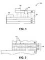
- FIG. 1depicts an exemplary photodetector including a photonic crystal resonant cavity in accordance with the present teachings.
- FIG. 2depicts an exemplary photodetector including a photonic crystal resonant cavity in a quantum dot structure in accordance with the present teachings.
- FIG. 3depicts a top view of a hexagonal pattern of cavities within an active region forming a photonic crystal resonant cavity in accordance with the present teachings.
- FIG. 4depicts an exemplary photodetector including a photonic crystal resonant cavity in a quantum well structure in accordance with the present teachings.
- FIG. 5depicts an exemplary photodetector including a photonic crystal resonant cavity in a DWELL structure in accordance with the present teachings.
- FIG. 6depicts an exemplary photodetector including a photonic crystal resonant cavity in a quantum dot structure in accordance with the present teachings.
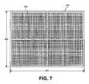
- FIG. 7depicts an exemplary focal plane array in accordance with the present teachings.
- FIGS. 1-7depict exemplary embodiments of devices that include a photonic crystal resonant cavity.
- the term “photonic crystal resonant cavity,” “photon controlling cavity,” and “photonic crystal”are used interchangeably and refer to a structure comprising a periodically varying index of refraction between, for example, a high index value and a low index value, and formed by one or more defects, such as, for example, cavities.
- the photonic crystal resonant cavitycan operate as a resonant structure to enhance the response of a device at one or more wavelengths.
- the devicescan include but are not limited to sensors, focal plane arrays, lasers, solar cells, diodes, and thermo-photovoltaic devices.
- the photodetectors including a photonic crystal resonant cavitycan, for example, demonstrate increased responsivity and quantum efficiency, lower the operating temperature, and/or be used to form a hyperspectral detector.
- FIG. 1depicts an exemplary device using a photonic crystal resonant cavity.
- An exemplary photodetector 100can include a first contact layer 130 , a second contact layer 180 , and an active region 140 disposed between first contact layer 130 and second contact layer 180 .
- Photodetector 100can further include a photonic crystal resonant cavity 150 .
- the photonic crystals resonant cavities disclosed hereinare each formed by a plurality of cavities in the active area, for example, as depicted in FIGS. 1-6 . However, for ease of illustration, only a portion of the cavities will be identified in the figures with a reference number.
- the photonic crystals resonant cavitiesare formed by a plurality of cavities arranged in a desired pattern.
- Photodetector 100can also include a substrate layer 110 , a buffer layer 120 formed on substrate 110 , a first contact 190 , and a second contact 195 .
- substrate layer 110can provide a surface to build the device on and also can provide structural integrity to the completed device.
- Substrate 110 and buffer layers 120 and 180can be conductive or insulating depending on the desired optical and electrical properties.
- Substrate layer 110can be formed of materials know to one of ordinary skill in the art, such as, for example, materials including gallium, indium, aluminum, silicon, silicon oxide, sapphire, gallium arsenide, diamond, silicon carbide, arsenic, and phosphorus.
- Buffer layer 120can also be formed of materials known to one of ordinary skill in the art.
- buffer layer 120can initiate proper growth conditions, establish the desired conductivity between substrate 110 and contact 130 , and/or serve as an etch stop layer.
- First contact 190 and second contact 195can be used to apply a bias voltage to photodector 100 . They can be formed of metal or other conductive materials known to one of ordinary skill in the art. First contact layer 130 and second contact layer 180 can also be formed of materials known to one of ordinary skill in the art, such as, for example, n-doped GaAs and doped as desired, or indium-tin-oxide. In various embodiments, contact layer 130 and 180 can act as a collector and/or emitter for the device.
- active region 140can be a quantum dot structure.
- the quantum dot structure forming active region 140can include quantum dot layers 142 and 144 separated by barrier layers 141 , 143 , and 145 .
- quantum dot layers 142 and 144include InGaAs, AlInAs, InP, and other alloys of AlGaInAsP on GaAs, and InGaAs on InP.
- Barrier layers 141 , 143 , and 145can be, for example, AlGaAs or AlGaInP doped to provide carriers for conductivity.
- Barrier layers 141 , 143 , and 145can be continuously doped or modulation doped.
- Active region 140 including a quantum dot structurecan be formed by methods known to one of ordinary skill in the art, examples of which are disclosed in U.S. Pat. No. 6,239,449, which is incorporate by reference in its entirety herein.
- Photonic crystal 150can be formed in active region 140 through the quantum dot structure as depicted in FIG. 2 .
- active region 140is depicted in FIG. 2 as including two quantum dot layers, one of ordinary skill in the art will understand that less than two or more than two quantum dot layers can be used.
- the barrier layers and quantum dot layerscan, respectively, have the same nominal composition and/or thickness.
- the alloy composition, doping and thicknesscan be tailored for a desired spectral response.
- photonic crystal resonant cavity 150is depicted in FIG. 2 having four cavities for ease of illustration, one of ordinary skill in the art will understand that the number and arrangement of the cavities can vary as desired and that other arrays (patterns) and number of cavities can be used.
- Photonic crystal resonant cavity 150can be a structure having a periodically varying index of refraction between, for example, a high index value and a low index value, and formed by one or more defects.
- Photonic crystal resonant cavity 150can be formed by, for example a plurality of localized defects in active region 140 , such as, for example, a plurality of line defects. Each of the plurality of line defects will have a refractive index different than the refractive index of the material comprising active region 140 .
- the defects, such as line defectscan be cavities or holes formed by e-beam lithography. The cavities or holes can be filled with air, liquid, or other material with a different index of refraction from the active layer materials.
- the cavities or holescan also be formed by other methods known to one of ordinary skill in the art, such as, for example, lithography and etching.
- FIG. 3is a top view of active region 140 showing a hexagonal array of air holes forming photonic crystal resonant cavity 150 .
- contacts 190 and 195can be biased. Incident light received by photodectector 100 can then affect the current between contacts 190 and 195 . Characteristics of the incident light can then be determined from the measured change in current. Photodectector 100 can also be biased in such a way that a change in voltage can provide similar information.
- Each hole of photonic crystal resonant cavity 150can serve as a small modal area waveguide tailored to have a small group dispersion. As such, the holes can function as a resonant cavity for light having a wavelength similar to the periodicity of the holes and can narrow and amplify the response.
- active region 140can be a quantum well structure.
- a quantum well structure 140can include active layers 147 and 149 , and barrier layers 141 , 143 , and 145 .
- Active layers 147 and 149can be formed of materials known to one of ordinary skill in the art including GaAs.
- Barrier layers 141 , 143 , and 145can also be formed of materials known to one of ordinary skill in the art and can include aluminum, gallium, and arsenide alloys. Although two active layers stacked with three barrier layers is depicted in FIG. 4 , additional active layers bounded by additional barrier layers is contemplated.
- Active region 140 including a quantum well structurecan be formed by methods known to one of ordinary skill in the art.
- Photonic crystal resonant cavity 150can be formed in the layers of active region 140 by, for example, electron beam lithography. Although photonic crystal resonant cavity 150 is depicted in FIG. 4 having four cavities for ease of illustration, one of ordinary skill in the art will understand that the number and arrangement of the cavities is exemplary and that other arrays and number of cavities can be used.
- active region 140can be a dots-in-well (DWELL) structure.
- DWELL structures and methods for forming DWELL structuresare describe in an article entitled “Effect of Well Width on Three-Color Quantum Dots-in-a Well Infrared Detectors,” IEEE Photonics Technology Letters, vol. 17, no. 5, May 2005, which is incorporated by reference in its entirety herein.
- a photodetector 500can include a first contact layer 530 , a second contact layer 580 , an active region 540 , and a photonic crystal resonant cavity 550 within active region 540 .
- Photodetector 500can further include substrate 510 , and contacts 590 , 591 , 595 , and 596 .
- contact layers 530 and 580can be n-doped GaAs layers.
- Active region 540can include barrier layers 541 and 545 formed of GaAs.
- Active region 540can further include a quantum dot layer 543 embedded in quantum well layers 542 and 544 .
- quantum dot layer 543 and quantum well layers 542can be doped InAs quantum dots in InGaAs alloy quantum wells.
- additional stacks of quantum dot layers embedded between quantum well layerscan be included between barrier layers 541 and 545 .
- Active region 540can further include a photonic crystal resonant cavity 550 formed by a plurality of cavities.
- the cavitiescan be formed in active region 540 by, for example, e-beam lithography.
- the cavitiescan further form a pattern, for example, as shown in FIG. 3 .
- a hyperspectral detectorincluding a photonic crystal resonant cavity tuned to two or more particular spectral bandwidths
- active region 640can include two or more quantum dot layers 642 , 644 bound by barrier layers 641 , 643 , 645 .
- Each quantum dot layer 642 and 644can include quantum dots with different compositions, sizes, and spacing to optimize detection of particular wavelengths.
- a photonic crystal resonant cavity 150can then be formed in active region 640 to optimize resonance at the particular wavelengths by changing the number, arrangement and/or size of the cavities.
- holes 151can be sized differently than holes 152 .
- a focal plane arraycan be formed by a plurality of photodetectors.
- Each of the plurality of photodetectorscan include a photonic crystal resonant cavity, as shown, for example, in FIGS. 1-6 .
- each of the plurality of photodetectorcan detect multiple wavelengths of light.
- the plurality of photodetectorscan be arranged to form a pixel.
- a focal plane array 700can then be formed by a plurality of pixels 701 .
- a 640 by 480 array of pixelscan form focal plane array 700 .
- the number of photodetectors in each pixel and the number of pixelsis exemplary, and that other embodiments are contemplated.
- the term “one or more of” with respect to a listing of items such as, for example, A and B,means A alone, B alone, or A and B.
Landscapes
- Engineering & Computer Science (AREA)
- Chemical & Material Sciences (AREA)
- Nanotechnology (AREA)
- Physics & Mathematics (AREA)
- Crystallography & Structural Chemistry (AREA)
- Mathematical Physics (AREA)
- Theoretical Computer Science (AREA)
- Life Sciences & Earth Sciences (AREA)
- Biophysics (AREA)
- Optics & Photonics (AREA)
- Light Receiving Elements (AREA)
Abstract
Description
Claims (15)
Priority Applications (1)
| Application Number | Priority Date | Filing Date | Title |
|---|---|---|---|
| US11/225,006US7659536B2 (en) | 2004-09-14 | 2005-09-14 | High performance hyperspectral detectors using photon controlling cavities |
Applications Claiming Priority (2)
| Application Number | Priority Date | Filing Date | Title |
|---|---|---|---|
| US60990204P | 2004-09-14 | 2004-09-14 | |
| US11/225,006US7659536B2 (en) | 2004-09-14 | 2005-09-14 | High performance hyperspectral detectors using photon controlling cavities |
Publications (2)
| Publication Number | Publication Date |
|---|---|
| US20060054880A1 US20060054880A1 (en) | 2006-03-16 |
| US7659536B2true US7659536B2 (en) | 2010-02-09 |
Family
ID=36032952
Family Applications (1)
| Application Number | Title | Priority Date | Filing Date |
|---|---|---|---|
| US11/225,006Expired - Fee RelatedUS7659536B2 (en) | 2004-09-14 | 2005-09-14 | High performance hyperspectral detectors using photon controlling cavities |
Country Status (1)
| Country | Link |
|---|---|
| US (1) | US7659536B2 (en) |
Cited By (7)
| Publication number | Priority date | Publication date | Assignee | Title |
|---|---|---|---|---|
| US20080080579A1 (en)* | 2006-07-13 | 2008-04-03 | California Institute Of Technology | Electrically pumped low-threshold ultra-small photonic crystal lasers |
| US20090174022A1 (en)* | 2006-03-24 | 2009-07-09 | Seth Coe-Sullivan | Hyperspectral imaging device |
| US8446592B1 (en) | 2008-08-04 | 2013-05-21 | Stc.Unm | Scanning phase intracavity nanoscope |
| US9143702B2 (en) | 2011-08-01 | 2015-09-22 | The Trustees Of Columbia University In The City Of New York | Lens-free planar imager using an optical resonator |
| US9212948B2 (en) | 2012-11-07 | 2015-12-15 | The Trustees Of Columbia University In The City Of New York | Lossless hyperspectral imaging |
| US9599770B2 (en) | 2012-03-30 | 2017-03-21 | The Trustees Of Columbia University In The City Of New York | Graphene photonics for resonator-enhanced electro-optic devices and all-optical interactions |
| US9778113B2 (en) | 2011-10-19 | 2017-10-03 | The Trustees Of Columbia University In The City Of New York | Ultracompact fabry-perot array for ultracompact hyperspectral imaging |
Families Citing this family (11)
| Publication number | Priority date | Publication date | Assignee | Title |
|---|---|---|---|---|
| US20060067605A1 (en)* | 2004-09-30 | 2006-03-30 | Laura Wills Mirkarimi | Photonic crystal optical temperature measuring system |
| WO2006125272A1 (en)* | 2005-05-27 | 2006-11-30 | Newsouth Innovations Pty Limited | Resonant defect enhancement of current transport in semiconducting superlattices |
| KR100750508B1 (en)* | 2005-12-06 | 2007-08-20 | 한국전자통신연구원 | Quantum Dot Laser Diode and Manufacturing Method Thereof |
| US8071945B2 (en)* | 2007-08-01 | 2011-12-06 | Stc.Unm | Infrared retina |
| CN101777599B (en)* | 2010-02-25 | 2012-01-11 | 华中科技大学 | Exciton photodetector for optical communication and preparation method thereof |
| US10539297B2 (en) | 2011-06-20 | 2020-01-21 | Crystalplex Corporation | Quantum dot containing light module |
| JP6135240B2 (en)* | 2013-03-28 | 2017-05-31 | 日本電気株式会社 | Photoelectric converter and light detection method |
| US9520514B2 (en)* | 2013-06-11 | 2016-12-13 | National Taiwan University | Quantum dot infrared photodetector |
| CN105047751B (en)* | 2015-06-02 | 2017-01-18 | 中国科学院上海技术物理研究所 | Liquid-phase epitaxial preparation method for indium arsenide thermophotovoltaic battery with barrier layer structure |
| CN105548033A (en)* | 2016-01-15 | 2016-05-04 | 华东师范大学 | Quantum dot embedded spectrograph |
| CN110264881B (en)* | 2019-06-20 | 2021-09-24 | 京东方科技集团股份有限公司 | Display device and manufacturing method |
Citations (10)
| Publication number | Priority date | Publication date | Assignee | Title |
|---|---|---|---|---|
| US4503447A (en)* | 1982-07-16 | 1985-03-05 | The United States Of America As Represented By The Secretary Of The Army | Multi-dimensional quantum well device |
| US5332681A (en)* | 1992-06-12 | 1994-07-26 | The United States Of America As Represented By The Secretary Of The Navy | Method of making a semiconductor device by forming a nanochannel mask |
| US5539206A (en)* | 1995-04-20 | 1996-07-23 | Loral Vought Systems Corporation | Enhanced quantum well infrared photodetector |
| US6239449B1 (en) | 1998-05-05 | 2001-05-29 | National Research Council Of Canada | Quantum dot infrared photodetectors (QDIP) |
| US20010012149A1 (en)* | 1997-10-30 | 2001-08-09 | Shawn-Yu Lin | Optical elements comprising photonic crystals and applications thereof |
| US6355939B1 (en)* | 1998-11-03 | 2002-03-12 | Lockheed Martin Corporation | Multi-band infrared photodetector |
| US20020167984A1 (en)* | 2001-01-11 | 2002-11-14 | Axel Scherer | Compact electrically and optically pumped multi-wavelength nanocavity laser, modulator and detector arrays and method of making the same |
| US20040021138A1 (en)* | 2000-07-28 | 2004-02-05 | Shields Andrew James | Optical device and a method of making an optical device |
| US20040124409A1 (en)* | 2002-09-19 | 2004-07-01 | Hiroji Ebe | Quantum optical semiconductor device |
| US20050212045A1 (en)* | 2004-03-24 | 2005-09-29 | Matsushita Electric Industrial Co., Ltd. | Photo-detecting device |
- 2005
- 2005-09-14USUS11/225,006patent/US7659536B2/ennot_activeExpired - Fee Related
Patent Citations (10)
| Publication number | Priority date | Publication date | Assignee | Title |
|---|---|---|---|---|
| US4503447A (en)* | 1982-07-16 | 1985-03-05 | The United States Of America As Represented By The Secretary Of The Army | Multi-dimensional quantum well device |
| US5332681A (en)* | 1992-06-12 | 1994-07-26 | The United States Of America As Represented By The Secretary Of The Navy | Method of making a semiconductor device by forming a nanochannel mask |
| US5539206A (en)* | 1995-04-20 | 1996-07-23 | Loral Vought Systems Corporation | Enhanced quantum well infrared photodetector |
| US20010012149A1 (en)* | 1997-10-30 | 2001-08-09 | Shawn-Yu Lin | Optical elements comprising photonic crystals and applications thereof |
| US6239449B1 (en) | 1998-05-05 | 2001-05-29 | National Research Council Of Canada | Quantum dot infrared photodetectors (QDIP) |
| US6355939B1 (en)* | 1998-11-03 | 2002-03-12 | Lockheed Martin Corporation | Multi-band infrared photodetector |
| US20040021138A1 (en)* | 2000-07-28 | 2004-02-05 | Shields Andrew James | Optical device and a method of making an optical device |
| US20020167984A1 (en)* | 2001-01-11 | 2002-11-14 | Axel Scherer | Compact electrically and optically pumped multi-wavelength nanocavity laser, modulator and detector arrays and method of making the same |
| US20040124409A1 (en)* | 2002-09-19 | 2004-07-01 | Hiroji Ebe | Quantum optical semiconductor device |
| US20050212045A1 (en)* | 2004-03-24 | 2005-09-29 | Matsushita Electric Industrial Co., Ltd. | Photo-detecting device |
Non-Patent Citations (5)
| Title |
|---|
| Ariyawansa, IEEE Photonics Technology Letters, vol. 17, No. 5 (2005) pp. 1064-1066. |
| Eui-Tae et al., "Tailoring detection bands of InAs quantum-dot infrared photodetectors using In.subx.Ga.sub1-x.As strain-relieving quantum wells", Applied Physics Letters, vol. 79, No. 20, Nov. 2001.* |
| Moosburger et al., Nanofabrication of high quality photonic crystal for integrated optics circuits, Nanotechnology, vol. 13, 2002, pp. 341-345.* |
| Raghavan et al., "High-responsivity, normal-incidence long-wave infrared (lambda ~ 7.2 micrometers) InAs/In sub0.15 Ga sub0.85 As dots-in-well detector", Applied Physics Letters, vol. 81, No. 8, p. 1369, Aug. 2002.* |
| Raghavan et al., "High-responsivity, normal-incidence long-wave infrared (lambda ˜ 7.2 micrometers) InAs/In sub0.15 Ga sub0.85 As dots-in-well detector", Applied Physics Letters, vol. 81, No. 8, p. 1369, Aug. 2002.* |
Cited By (9)
| Publication number | Priority date | Publication date | Assignee | Title |
|---|---|---|---|---|
| US20090174022A1 (en)* | 2006-03-24 | 2009-07-09 | Seth Coe-Sullivan | Hyperspectral imaging device |
| US8610232B2 (en)* | 2006-03-24 | 2013-12-17 | Qd Vision, Inc. | Hyperspectral imaging device |
| US20080080579A1 (en)* | 2006-07-13 | 2008-04-03 | California Institute Of Technology | Electrically pumped low-threshold ultra-small photonic crystal lasers |
| US7813401B2 (en)* | 2006-07-13 | 2010-10-12 | California Institute Of Technology | Electrically pumped low-threshold ultra-small photonic crystal lasers |
| US8446592B1 (en) | 2008-08-04 | 2013-05-21 | Stc.Unm | Scanning phase intracavity nanoscope |
| US9143702B2 (en) | 2011-08-01 | 2015-09-22 | The Trustees Of Columbia University In The City Of New York | Lens-free planar imager using an optical resonator |
| US9778113B2 (en) | 2011-10-19 | 2017-10-03 | The Trustees Of Columbia University In The City Of New York | Ultracompact fabry-perot array for ultracompact hyperspectral imaging |
| US9599770B2 (en) | 2012-03-30 | 2017-03-21 | The Trustees Of Columbia University In The City Of New York | Graphene photonics for resonator-enhanced electro-optic devices and all-optical interactions |
| US9212948B2 (en) | 2012-11-07 | 2015-12-15 | The Trustees Of Columbia University In The City Of New York | Lossless hyperspectral imaging |
Also Published As
| Publication number | Publication date |
|---|---|
| US20060054880A1 (en) | 2006-03-16 |
Similar Documents
| Publication | Publication Date | Title |
|---|---|---|
| US10446701B2 (en) | In-plane resonant-cavity infrared photodetectors with fully-depleted absorbers | |
| US7659536B2 (en) | High performance hyperspectral detectors using photon controlling cavities | |
| US10062794B2 (en) | Resonant-cavity infrared photodetectors with fully-depleted absorbers | |
| US8637951B2 (en) | Semiconductor light receiving element and optical communication device | |
| EP3769343B1 (en) | Photodetector | |
| EP3769342A1 (en) | In-plane resonant-cavity infrared photodetectors with fully-depleted absorbers | |
| WO2005038997A2 (en) | Intersubband detector with avalanche multiplier region | |
| JP2017500743A (en) | Low noise quantum detector and method for manufacturing such photon detector | |
| US5965899A (en) | Miniband transport quantum well detector | |
| JP2004104085A (en) | Avalanche Phototransistor | |
| JP2007227744A (en) | Quantum dot optical semiconductor device and manufacturing method thereof | |
| JP4386191B2 (en) | Optical element | |
| WO2008011152A2 (en) | Longwave infrared photodetector | |
| Bois et al. | Technology of multiple quantum well infrared detectors | |
| EP0648377B1 (en) | Miniband transport quantum well detector | |
| JP4331428B2 (en) | Intersubband Transition Quantum Well Photodetector | |
| Ralston et al. | Novel molecular‐beam epitaxially grown GaAs/AlGaAs quantum well structures for infrared detection and integrated optics at 3–5 and 8–12 μm | |
| JP2006196788A (en) | Infrared detector | |
| Liu et al. | Tunable metamorphic resonant cavity enhanced InGaAs photodetectors grown on GaAs substrates | |
| LU100953B1 (en) | Photodetector | |
| WO1999017341A2 (en) | Dual band infrared detector using step multiquantum wells with superlattice barriers | |
| JPH0353565A (en) | Multi-quantum well structure photodetector | |
| Palaferri et al. | Antenna-coupled microcavity enhanced THz photodetectors | |
| Liu et al. | Photon upconversion devices | |
| Song et al. | Characteristics of InAs QDs/GaAs RC-SACM APD on the Etching Process of the Active-Mesa |
Legal Events
| Date | Code | Title | Description |
|---|---|---|---|
| AS | Assignment | Owner name:SCIENCE & TECHNOLOGY CORPORATION @UNM,NEW MEXICO Free format text:ASSIGNMENT OF ASSIGNORS INTEREST;ASSIGNOR:THE UNIVERSITY OF NEW MEXICO;REEL/FRAME:017263/0408 Effective date:20040820 Owner name:THE UNIVERSITY OF NEW MEXICO,NEW MEXICO Free format text:ASSIGNMENT OF ASSIGNORS INTEREST;ASSIGNORS:KRISHNA, SANJAY;PAINTER, OSKAR;SIGNING DATES FROM 20040726 TO 20040803;REEL/FRAME:017263/0398 Owner name:SCIENCE & TECHNOLOGY CORPORATION @UNM, NEW MEXICO Free format text:ASSIGNMENT OF ASSIGNORS INTEREST;ASSIGNOR:THE UNIVERSITY OF NEW MEXICO;REEL/FRAME:017263/0408 Effective date:20040820 Owner name:THE UNIVERSITY OF NEW MEXICO, NEW MEXICO Free format text:ASSIGNMENT OF ASSIGNORS INTEREST;ASSIGNORS:KRISHNA, SANJAY;PAINTER, OSKAR;REEL/FRAME:017263/0398;SIGNING DATES FROM 20040726 TO 20040803 | |
| AS | Assignment | Owner name:STC.UNM,NEW MEXICO Free format text:CHANGE OF NAME;ASSIGNOR:SCIENCE & TECHNOLOGY CORPORATION @ UNM;REEL/FRAME:023687/0266 Effective date:20060914 | |
| STCF | Information on status: patent grant | Free format text:PATENTED CASE | |
| AS | Assignment | Owner name:CALIFORNIA INSTITUTE OF TECHNOLOGY, CALIFORNIA Free format text:ASSIGNMENT OF ASSIGNORS INTEREST;ASSIGNOR:STC.UNM;REEL/FRAME:024794/0036 Effective date:20100520 | |
| AS | Assignment | Owner name:AIR FORCE, UNITED STATES, VIRGINIA Free format text:CONFIRMATORY LICENSE;ASSIGNORS:CALIFORNIA INSTITUTE OF TECHNOLOGY;FA9550-06-1-0443;REEL/FRAME:024879/0309 Effective date:20090819 | |
| AS | Assignment | Owner name:AIR FORCE, UNITED STATES, VIRGINIA Free format text:CONFIRMATORY LICENSE;ASSIGNOR:CALIFORNIA INSTITUTE OF TECHNOLOGY;REEL/FRAME:025227/0333 Effective date:20090819 | |
| CC | Certificate of correction | ||
| FPAY | Fee payment | Year of fee payment:4 | |
| FEPP | Fee payment procedure | Free format text:MAINTENANCE FEE REMINDER MAILED (ORIGINAL EVENT CODE: REM.) | |
| FEPP | Fee payment procedure | Free format text:7.5 YR SURCHARGE - LATE PMT W/IN 6 MO, SMALL ENTITY (ORIGINAL EVENT CODE: M2555) | |
| MAFP | Maintenance fee payment | Free format text:PAYMENT OF MAINTENANCE FEE, 8TH YR, SMALL ENTITY (ORIGINAL EVENT CODE: M2552) Year of fee payment:8 | |
| FEPP | Fee payment procedure | Free format text:MAINTENANCE FEE REMINDER MAILED (ORIGINAL EVENT CODE: REM.); ENTITY STATUS OF PATENT OWNER: SMALL ENTITY | |
| LAPS | Lapse for failure to pay maintenance fees | Free format text:PATENT EXPIRED FOR FAILURE TO PAY MAINTENANCE FEES (ORIGINAL EVENT CODE: EXP.); ENTITY STATUS OF PATENT OWNER: SMALL ENTITY | |
| STCH | Information on status: patent discontinuation | Free format text:PATENT EXPIRED DUE TO NONPAYMENT OF MAINTENANCE FEES UNDER 37 CFR 1.362 | |
| FP | Lapsed due to failure to pay maintenance fee | Effective date:20220209 |