US7659513B2 - Low terahertz source and detector - Google Patents
Low terahertz source and detectorDownload PDFInfo
- Publication number
- US7659513B2 US7659513B2US11/641,678US64167806AUS7659513B2US 7659513 B2US7659513 B2US 7659513B2US 64167806 AUS64167806 AUS 64167806AUS 7659513 B2US7659513 B2US 7659513B2
- Authority
- US
- United States
- Prior art keywords
- charged particles
- ultra
- electromagnetic radiation
- different conditions
- emr
- Prior art date
- Legal status (The legal status is an assumption and is not a legal conclusion. Google has not performed a legal analysis and makes no representation as to the accuracy of the status listed.)
- Active - Reinstated, expires
Links
Images


Classifications
- H—ELECTRICITY
- H01—ELECTRIC ELEMENTS
- H01J—ELECTRIC DISCHARGE TUBES OR DISCHARGE LAMPS
- H01J25/00—Transit-time tubes, e.g. klystrons, travelling-wave tubes, magnetrons
- G—PHYSICS
- G01—MEASURING; TESTING
- G01J—MEASUREMENT OF INTENSITY, VELOCITY, SPECTRAL CONTENT, POLARISATION, PHASE OR PULSE CHARACTERISTICS OF INFRARED, VISIBLE OR ULTRAVIOLET LIGHT; COLORIMETRY; RADIATION PYROMETRY
- G01J3/00—Spectrometry; Spectrophotometry; Monochromators; Measuring colours
- G01J3/28—Investigating the spectrum
- G01J3/42—Absorption spectrometry; Double beam spectrometry; Flicker spectrometry; Reflection spectrometry
- H—ELECTRICITY
- H01—ELECTRIC ELEMENTS
- H01J—ELECTRIC DISCHARGE TUBES OR DISCHARGE LAMPS
- H01J47/00—Tubes for determining the presence, intensity, density or energy of radiation or particles
Definitions
- Thisrelates in general to one or more receivers for detecting electromagnetic signals in the low terahertz range and in one embodiment to at least one detection system for detecting low terahertz radiation produced by a microresonant structure.
- micro- and nano-resonant structuresare described that react in now-predictable manners when an electron beam is passed in their proximity.
- energy of the electron beamto be converted into the energy of electromagnetic radiation (e.g., light) when the electron beam passes nearby.
- electromagnetic radiatione.g., light
- the electron beampasses near the structure, it excites synchronized oscillations of the electrons in the structure (surface plasmons) and/or electrons in the beam. As often repeated as the many electrons in a beam pass, these surface plasmons result in reemission of detectable photons as electromagnetic radiation (EMR).
- EMRelectromagnetic radiation
- Electromagnetic radiation of known frequencies (and amounts)is transmitted into an area or structure to be tested. By detecting whether and how the transmitted electromagnetic radiation is reflected, absorbed or transmitted through the object under test, detections can be achieved. Alternatively, by detecting the presence of electromagnetic radiation leaving an object under examination at one or more frequencies other than the frequency that was transmitted into the object, detection of other materials can similarly be made.
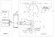
- FIG. 1is a schematic view of a transmitter and a receiver system
- FIG. 2is an alternative resonant structure for a receiver
- FIGS. 3 and 4are schematic representations of a portion of a resonant structure detecting the absence and presence of a signal of interest, respectively;
- FIG. 5is a perspective view of two resonant structures for a receiver
- FIG. 6is a non-empirical, non-experimental representation of the theoretical absorption versus wavelength for a structure such as in FIG. 5 ;
- FIG. 7is an alternative example receiver
- FIG. 8is an alternative example receiver
- FIG. 9is an alternative example receiver
- FIG. 10is an alternative example receiver
- FIG. 11is an alternative example receiver
- FIG. 12is an alternative example receiver
- FIG. 13is an alternative example receiver
- FIG. 14is an example secondary electron shield on an example receiver
- FIG. 15is an example secondary detector
- FIG. 16is a close-up view of a portion of the secondary detector of FIG. 15 ;
- FIG. 17is a representation of experimental results from a resonant receiver structure
- FIG. 18is a representation of experimental results from a resonant receiver structure
- FIG. 19is a block diagram of the general components of a multi-frequency receiver.
- FIGS. 20-23are block diagrams of various multi-frequency matrices of receivers for receiving signals at plural locations.
- a transmitter 1can include an ultra-small resonant structure, such as any one described in U.S. patent application Ser. Nos. 11/238,991; 11/243,476; 11/243,477; 11/325,448; 11/325,432; 11/302,471; 11/325,571; 11/325,534; 11/349,963; and/or 11/353,208 (each of which is identified more particularly above).
- the resonant structures in the transmittercan be manufactured in accordance with any of U.S. application Ser. Nos. 10/917,511; 11/350,812; or 11/203,407 (each of which is identified more particularly above) or in other ways. Their sizes and dimensions can be selected in accordance with the principles described in those applications and, for the sake of brevity, will not be repeated herein.
- the contents of the applications described aboveare assumed to be known to the reader.
- the transmitter 1can also comprise any macroscopic or microscopic electromagnetic radiation (EMR) emitter emitting in the low terahertz range, and can include even prior art low terahertz transmitters, semiconductors or other low terahertz-emitting devices.
- EMRelectromagnetic radiation
- the transmitter 1may be operated in association with a controller 18 , which may be part of the transmitter or may be separated from the transmitter 1 (the former embodiment is shown in FIG. 1 ).
- the controller 18is designed to selectively activate at least one electromagnetic radiation (EMR) source 17 that transmits EMR 15 t to the receiver 10 .
- EMRelectromagnetic radiation
- the at least one EMR source 17is controlled by the controller 18 such one or more frequencies of EMR are emitted from the transmitter 1 as EMR 15 t .
- the receiver 10then receives EMR 15 r .
- the received EMR 15 rshould be understood to include any EMR that is received at the receiver and dependent on at least one of the transmitted EMR 15 t and the object 5 under test and may just be referred to as 15 .
- Such EMRmay include, but is not limited to, unabsorbed EMR 15 t , reflected EMR 15 a , and secondary EMR 15 b (at a frequency that is either other than or the same as the frequency of the incident EMR) generated by the object 5 itself when exposed to EMR 15 t .
- the amount of received EMR 15 rdepends on what the object 5 under test contains.
- the object 5 under examinationis depicted as a cylinder, but any object, person, material, chemical, element, etc. may be used as the “object.”
- Materials that may be detected in an object 5include, but are not limited to, biologically active materials and explosives.
- the objectmay be placed in a specialized container which is then inserted into a machine for testing, or the object may be in an open area where the open area itself is then subjected to EMR.
- An example of an open air environmentincludes passenger screening systems in which a potential passenger (e.g., an airline passenger) first walks through a detector area where the passenger can be tested prior to boarding.
- An example of testing using machines into which an object is placedincludes a swab analyzer into which a swab is placed after the swab has been rubbed over an article of interest (e.g., luggage).
- the detectorcan detect radiation emitted by the objects. This could be radiation due to thermal emission or due to other causes such as chemical or molecular vibrational EMR emission. This EMR could also consist partly or fully of reflected and transmitted background EMR
- the controller 18can pulse the at least one EMR source 17 and images can be created based on delay time to the receiver. Images or “snap-shots” may also be taken in series to capture how a sample is changing or reacting (e.g., fluorescing or otherwise emitting EMR) for some time after receiving an EMR pulse or its condition can be monitored continuously if the source is left on continuously or repeatedly pulsed.
- images or “snap-shots”may also be taken in series to capture how a sample is changing or reacting (e.g., fluorescing or otherwise emitting EMR) for some time after receiving an EMR pulse or its condition can be monitored continuously if the source is left on continuously or repeatedly pulsed.
- the receiver 10includes cathode 20 , anode 19 , optional energy anode 23 , ultra-small resonant structures 12 , Faraday cup or other receiving electrode 14 , electrode 24 , and differential current detector 16 .
- the status of the receiver 10will now be described in the case where the receiver 10 is not being stimulated by the presence of EMR 15 .
- the cathode 20produces an electron beam 13 , which is steered and focused by anode 19 and accelerated by energy anode 23 .
- the electron beam 13is directed to pass close to but not touching one or more ultra-small resonant structures 12 .
- resonant structures in the receiver 10can be, by way of example, one of those described in U.S. patent application Ser. Nos. 11/238,991; 11/243,476; 11/243,477; 11/325,448; 11/325,432; 11/302,471; 11/325,571; 11/325,534; 11/349,963; and/or 11/353,208 (each of which is identified more particularly above).
- the resonant structures in the receiver 10can be manufactured in accordance with any of U.S. application Ser. Nos. 10/917,511; 11/350,812; or 11/203,407 (each of which is identified more particularly above) or in other ways.
- the structuresare considered ultra-small when they embody at least one dimension that is smaller than the wavelength of light that they are detecting or emitting.
- the ultra-small structuresare employed in a vacuum environment. Methods of evacuating the environment where the beam 13 passes by the structures 12 can be selected from known evacuation methods.
- the electron beam 13passes energy anode 23 , which further accelerates the electrons in known fashion.
- the electron beam 13passes by the resonant structures 12 with the structures 12 having no significant effect on the path of the electron beam 13 .
- the electron beam 13thus follows, in general, the path 13 b .
- the electron beam 13proceeds past the structures 12 and is received by a Faraday cup or other detector electrode 14 .
- the Faraday cupwill receive and absorb the electron beam 13 .
- the path of the electron beamcan be altered even when the EMR 15 is not being received at the resonant structures, provided the path of the electron beam 13 is identifiable with the absence of the EMR 15 .
- the cathode 20produces the electron beam 13 , which is directed by the current anode 19 and energy anode 23 , past the resonant structures 12 .
- the EMR 15is inducing resonance on the resonant structures 12 .
- the ability of the EMR 15 to induce the electron resonanceis described in one or more of the above applications and is not repeated herein.
- the electron beam 13is deflected by the electron density oscillation effect causing the electron beam to deflected randomly from path 13 b (into the Faraday cup) and into one or more alternative paths depending on the surface charge at the moment at which the electron in the beam passes the resonant structure, such as paths 13 a or 13 c .
- paths 13 a and 13 cshould be understood to be any path that does not impact the detector electrode 14 .
- FIG. 1are not to scale—the amount of deflection of the electron beam may be exaggerated in FIG. 1 to illustrate the principle.
- the size of the Faraday cup or other detector electrode 14is selected so the deflected electron beam on path 13 a / 13 b misses the Faraday cup and instead is received at the electrode 24 .
- Differential current detector 16detects when the electron beam 13 is impacting the electrode 24 by detecting a differential current between the Faraday cup or other detector electrode 14 and the electrode 24 .
- Alternative methods of detecting the deflected electron beam other than the Faraday cup and electrodewill be recognizable to the artisan who understands from this description the structure and purpose of the receiver 10 .
- resonant structures 12can appear on one side of the electron beam 13 , as shown, or may appear on both sides of the electron beam 13 so the electron beam path is impacted by resonant structures as it passes between them.
- An example such structureis shown in FIG. 2 .
- the resonant structuresare no longer rectangular shaped (the structures could conceivably be any shape), but are instead triangular. The triangular shape may be preferable in altering the passing electron beam 13 due to concentration of the electromagnetic fields in the tips of the triangles as the electron resonant waves are excited by the incident EMR 15 .
- the EMR 15will not interact with the electron beam directly. That is, the electrons in the beam are so small and so dispersed and the photons of the EMR 15 are small and dispersed that practical interaction between them is essentially statistically non-existent.
- the EMR 15cannot be reliably transferred to the electronic structures of the receiver 10 by simple interaction of the EMR 15 with the electron beam 13 , we have provided a receiver that “holds” the information in the EMR on the resonant structures 12 via the activity of the surface plasmons long enough for the electron beam 13 passing by to interact with EMR 15 .
- the EMR 15is thus coupled onto the electron beam 13 (and thus to electronic circuit elements) when it was previously considered impossible to do so.
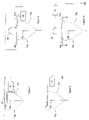
- FIGS. 3 and 4for simplicity we illustrate only one of the resonant structures 21 , but the artisan will recognize from the disclosure with respect to FIGS. 1 and 2 that more than one such structure can be presented in the receiver 10 .
- FIG. 3illustrates the electron beam 13 passing by the resonant structure 21 when the EMR 15 of interest is not being received (either from the transmitter 1 or from an emission of the object 5 ). As shown, the lack of EMR 15 of the desired frequency produces no appreciable effect between the resonant structure 21 and the passing electron beam 13 . Accordingly, the electron beam 13 passes generally straight along path 13 b and into the Faraday cup or other detector electrode 14 .
- FIG. 4illustrates the electron beam 13 passing by the resonant structure 21 when EMR 15 having the desired frequency is being received (either from the transmitter 1 or from an emission of the object 5 ).
- the EMR 15 having the desired frequencyis incident to the resonant structure 21 .
- the resonant structure 21responds to the EMR 15 having the desired frequency with the electrons moving on the surface 25 and creating a focused electric field at the tip of the triangular structure 21 .
- the electric fieldcauses the passing electron 13 to alter its otherwise straight path to the alternative path 13 a .
- the path 13 atakes the electron beam past the Faraday cup or other detector electrode 14 and onto the electrode 24 , where the electron beam is detected by the differential current detector 16 .
- the path of the deflected electron beam 13could be a scattering along multiple paths including paths 13 a and 13 c , as the resonating effect of the EMR 15 on the structures 21 changes the electric field at the tip.
- the altered pathswill each miss the detector 14 and thus the resonance on the structure 21 will still cause the electrons to meet the electrode 24 rather than the electrode 14 .
- the existence of the EMR 15is reflected in a detection of a current difference in the differential current detector 16 caused by the deflection of the electron beam 13 into the electrode 24 rather than the detector electrode 14 .
- the absence of the EMR 15is reflected in a detection of a different differential current value in the differential current detector 16 when the electron beam 13 is directed straight into the Faraday cup or other detector electrode 14 .
- the receiver 10can determine what EMR 15 r is received in the presence of transmitted EMR 15 t , the artisan can readily appreciate how the receiver can detect the presence or absence of a portion of interest of the received spectrum.
- a resonant structure 12 and/or 21will respond most effectively to a particular frequency of EMR 15 .
- the transmittertransmits EMR 15 t at a particular wavelength and the resonant structures 12 and 21 have geometries that respond to the wavelength to be detected 15 r .
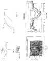
- FIG. 6illustrates the general principle (it is not reflective of any actual test) that ultra-small structures of particular geometries, such as those shown in FIG. 5 (showing height, width, depth and periodicity of resonant structures) will demonstrate absorption rates peaking at multiples of a particular wavelength.
- the present receiver 10is not limited to any particular resonant structure shape (many example shapes are described in the related patent applications identified above), but should preferably (though not necessarily) have one dimension smaller than the wavelength of the photon to be detected.
- the wavelength characteristics shown in FIG. 6can be ascertained for any given structure by empirically testing the structure. Applying EMR of varying frequencies and measuring the absorption, reflection, transmission, fluorescence, phase shift, change in polarity and/or any other property of an electromagnetic wave leads to a kind of the graph of FIG. 6 for any particular structure type, size, and periodicity.
- the characteristic frequency of absorptionis ascertained, it can either be adjusted to the frequency of the EMR 15 , or the EMR 15 can be adjusted in frequency to that of the receiver 10 . An estimate of the frequency response can be calculated as well.
- Emissionscan also be measured to help in design.
- One example empirical graphis shown in FIG. 17 where the Y-axis represents counts of electrons emitted versus finger length (i.e., the long dimension of resonant structure). The resultant peaks illustrate optimal finger lengths for the particular EMR frequency and can be used to shape the geometry of the resonant structures.
- FIGS. 7-13illustrate different forms of receivers that provide the same mechanism of detecting the EMR 15 , but with the resonant structures along the initial path of the charged particle beam removed for clarity.
- the electrode 14 acorresponds to the electrode 14 in FIG. 1 , except that the shape is flatter.
- FIG. 7illustrates the broader principle that the shape, size and characteristics of all of the electrodes shown can be modified from the ones described and shown herein and still accomplish the intended detection.
- the order of encounter of the electrodescan be altered; namely the “straight path” electrode 30 for the “absent” condition can appear to the electron beam 13 after passing the “altered path” electrode 14 b / 24 a for the “present” condition.
- the electrodes 14 b and 24 acan be separate electrodes electrically connected to the detector 16 , or they can be one doughnut-shaped electrode with the hole in the center providing the path for the electron beam 13 to pass when it is not be diverted or it could have rectangular or any other general shape which allows then unaltered path to pass.
- the detector 16need not detect the current difference between the “present” and “absent” electrodes, but can instead detect change in current in the “present” electrode(s).
- the “absent” electrodein the case of FIG. 8 the electrode 30 ) takes the electron beam to ground (or may capture it with a Faraday cup and employ it for power requirements of the electric circuits).
- FIG. 9illustrates a detector in which the detector 16 detects current conditions on the “absent” electrode 14 c and compares it to ground. It could alternatively do the same for the “present” electrode (instead or in addition to the “absent” electrode).
- FIG. 10illustrates the “present” electrodes 14 b / 24 a taking the electron beam to ground and the “absent” electrode 30 providing the detector 16 with a signal referenced to ground whenever the electron beam follows the non-deflected path 13 b.
- FIG. 11illustrates basically side-by-side electrodes 24 and 14 b .
- electrode 14 bslightly extends into the straight-line path 13 b so the “absent” condition is detected by it.
- Electrode 24is positioned to capture the electron beam when it is deflected to the 13 a path in the “present” condition.
- FIG. 12we illustrate detectors that provide improved sensitivity and noise-reduction by referencing the received electron beam to the cathode.
- FIG. 12the principle of the detector referenced to an electric characteristic of the cathode is shown.
- the example embodimentshows the “absent” electrode 14 a receiving the “absent” path 13 b and the “present” electrode 24 receiving the “present” paths 13 a and 13 c .
- the detectorreceives the beam and references it to an electrical characteristic that it receives from the cathode (or another element associated with the electron beam source). In that way, noise associated with the electron beam source can be cancelled.
- the “absent” electrodecan be grounded, Faraday cupped, etc.
- the “present” electrode 24is electrically coupled to the detector 16 . Inside detector 16 is a current detector 28 that measures the current between the cathode 20 and anode 19 .
- the current in that electrode 24is detected by the detector 16 (and then diverted ground, a Faraday cup, etc.) and referenced to the current detected by detector 28 such that noise in the electron beam source can be cancelled, improving detection sensitivity.
- the shield 29 a / 29 b in FIGS. 13 and 14illustrate an example option that can reduce the stray electrons. Specifically, it is advantageous to keep stray electrons out of the area where the electron beam 13 (either deflected or non-deflected) will be traveling to avoid collisions between the stray electrons and the electrons in the beam 13 .
- the shields 29 a and 29 bare grounded and sit in front of (relative to the beam path) the detector being employed in order to provide the stray electrons another “to-ground” attraction before they enter the area where the electron beam 13 is traveling.
- the shields 29 a and 29 bcan be employed with any type of detector (for example, any of FIGS. 7-12 ).
- FIGS. 15 and 16describe an optional electrode structure that will also better capture the electrons in the electron beam 13 , thereby reducing the possibility of stray electrons returning “up-stream” and interfering with the electron beam 13 .
- the electrode 60(which can be any of the electrode embodiments earlier described) is in the structural form of a baffle such that approaching electrons in the beam 13 have a multiple chance of being absorbed.
- FIG. 15only the “absent” electrode 60 is shown with the baffles, but the “present” detector electrode 61 can also (or instead) be baffled.
- the bafflesare more particularly shown in FIG.
- FIG. 18illustrates a graph of percent reflectivity (Y-axis) versus wavelength of EMR measured in nm (X-axis).
- Y-axispercent reflectivity
- X-axiswavelength of EMR measured in nm
- the dominant “dips” in the graphillustrate wavelengths of the EMR that were absorbed well by one or more of the resonant structures at the polarity shown. Other EMR frequencies and finger lengths could be mapped and used as alternatives.
- the graphis significant to show that the resonant structures are in fact absorbing the EMR energy.
- the graphis also significant in illustrating the effect of polarization angle on the absorption. In essence, the graph illustrates that absorption occurs and that it is enhanced when polarization of the EMR is parallel to the finger length.
- the graphs for polarization angles 0 and 180show large absorption at the dips and for angles 90 and 270, for example show lower absorption.
- plural receivers 10 1 . . . 10 ncan be repeated within an array of receivers such that series of frequencies can be detected.
- detection of EMR 15 at a single frequencymay be insufficient to distinguish between first and second chemicals, where the first chemical is of interest but the second chemical is not.
- the detection of possible emissions at one or more additional frequenciesmay enable the system to distinguish between the first and second chemicals if those chemicals absorb EMR or emit EMR differently.
- the array of receiversmay be designed to receive n different frequencies, where n is greater than 1.
- the signals from the array of receiversare then processed in circuitry (e.g., microprocessor circuitry or custom-designed circuitry) to determine whether a chemical/material of interest is present while excluding other chemicals/materials which are not of interest.
- the array of receivers 10 1 . . . 10 ncan be repeated in various configurations if/when signals need to be spatially resolved or to enable redundancy.
- FIG. 20illustrates a matrix of receivers where each row contains the ability to receive “n” different frequencies, where n is greater than or equal to 1.
- an array of receiverscan be repeated linearly.
- sets of receiverscan be grouped together, and then the sets of receivers are repeated throughout a matrix.
- receiver 22 and 23are illustrated as 4 receivers and 9 receivers per set, respectively, those of ordinary skill in the art will appreciate that any number of receivers can be in a set and then repeated throughout the matrix. Furthermore, the order of the receivers need not be the same in all sets and instead may be alternated, if desired.
- additional optical devicessuch as lens and deflectors may be required to properly direct the signals onto an array or matrix of receivers.
- the transmittermay include a modulated source of EMR.
- the modulated source of EMRcan enable the receiver to be tuned to the modulation for increased sensitivity.
- the receivermay therefore perform signal lock-in and phase sensitive detection.
- the above-described matrices and arrayscan be formed into any number of configurations and devices, such as focal planes, still cameras, moving picture/video cameras, etc. Furthermore, more than one type of receiver can be integrated into the same device. For example, various receivers for receiving one set of frequencies can be integrated into a single device. Such a combined device may include a video camera combined with a still camera or a video camera combined with a focal plane.
Landscapes
- Physics & Mathematics (AREA)
- Spectroscopy & Molecular Physics (AREA)
- General Physics & Mathematics (AREA)
- Measurement Of Radiation (AREA)
Abstract
Description
- 1. U.S. patent application Ser. No. 11/238,991, entitled “Ultra-Small Resonating Charged Particle Beam Modulator,” filed Sep. 30, 2005;
- 2. U.S. patent application Ser. No. 10/917,511, entitled “Patterning Thin Metal Film by Dry Reactive Ion Etching,” filed on Aug. 13, 2004;
- 3. U.S. application Ser. No. 11/203,407, entitled “Method Of Patterning Ultra-Small Structures,” filed on Aug. 15, 2005;
- 4. U.S. application Ser. No. 11/243,476, entitled “Structures And Methods For Coupling Energy From An Electromagnetic Wave,” filed on Oct. 5, 2005;
- 5. U.S. application Ser. No. 11/243,477, entitled “Electron beam induced resonance,” filed on Oct. 5, 2005;
- 6. U.S. application Ser. No. 11/325,448, entitled “Selectable Frequency Light Emitter from Single Metal Layer,” filed Jan. 5, 2006;
- 7. U.S. application Ser. No. 11/325,432, entitled, “Matrix Array Display,” filed Jan. 5, 2006;
- 8. U.S. application Ser. No. 11/302,471, entitled “Coupled Nano-Resonating Energy Emitting Structures,” filed Dec. 14, 2005;
- 9. U.S. application Ser. No. 11/325,571, entitled “Switching Micro-resonant Structures by Modulating a Beam of Charged Particles,” filed Jan. 5, 2006;
- 10. U.S. application Ser. No. 11/325,534, entitled “Switching Microresonant Structures Using at Least One Director,” filed Jan. 5, 2006;
- 11. U.S. application Ser. No. 11/350,812, entitled “Conductive Polymers for Electroplating,” filed Feb. 10, 2006;
- 12. U.S. application Ser. No. 11/349,963, entitled “Method and Structure for Coupling Two Microcircuits,” filed Feb. 9, 2006;
- 13. U.S. application Ser. No. 11/353,208, entitled “Electron Beam Induced Resonance,” filed Feb. 14, 2006;
- 14. U.S. application Ser. No. 11/400,280, entitled “Resonant Detectors for Optical Signals,” filed Apr. 10, 2006;
- 15. U.S. application Ser. No. 11/410,924, entitled “Selectable Frequency EMR Emitter,” filed Apr. 26, 2006;
- 16. U.S. application Ser. No. 11/411,129, entitled “Micro Free Electron Laser (FEL),” filed Apr. 26, 2006;
- 17. U.S. application Ser. No. 11/418,088, entitled “Heterodyne Receiver Using Resonant Structures,” filed May 5, 2006; and
- 18. U.S. application Ser. No. 11/418,118, entitled “Heterodyne Receiver Array Using Resonant Structures,” filed May 5, 2006.
Claims (18)
Priority Applications (1)
| Application Number | Priority Date | Filing Date | Title |
|---|---|---|---|
| US11/641,678US7659513B2 (en) | 2006-12-20 | 2006-12-20 | Low terahertz source and detector |
Applications Claiming Priority (1)
| Application Number | Priority Date | Filing Date | Title |
|---|---|---|---|
| US11/641,678US7659513B2 (en) | 2006-12-20 | 2006-12-20 | Low terahertz source and detector |
Publications (2)
| Publication Number | Publication Date |
|---|---|
| US20080149828A1 US20080149828A1 (en) | 2008-06-26 |
| US7659513B2true US7659513B2 (en) | 2010-02-09 |
Family
ID=39541485
Family Applications (1)
| Application Number | Title | Priority Date | Filing Date |
|---|---|---|---|
| US11/641,678Active - Reinstated2027-03-03US7659513B2 (en) | 2006-12-20 | 2006-12-20 | Low terahertz source and detector |
Country Status (1)
| Country | Link |
|---|---|
| US (1) | US7659513B2 (en) |
Cited By (9)
| Publication number | Priority date | Publication date | Assignee | Title |
|---|---|---|---|---|
| US20070272931A1 (en)* | 2006-05-05 | 2007-11-29 | Virgin Islands Microsystems, Inc. | Methods, devices and systems producing illumination and effects |
| US20090072698A1 (en)* | 2007-06-19 | 2009-03-19 | Virgin Islands Microsystems, Inc. | Microwave coupled excitation of solid state resonant arrays |
| US20090140178A1 (en)* | 2006-01-05 | 2009-06-04 | Virgin Islands Microsystems, Inc. | Switching micro-resonant structures by modulating a beam of charged particles |
| US20090230332A1 (en)* | 2007-10-10 | 2009-09-17 | Virgin Islands Microsystems, Inc. | Depressed Anode With Plasmon-Enabled Devices Such As Ultra-Small Resonant Structures |
| US7935930B1 (en)* | 2009-07-04 | 2011-05-03 | Jonathan Gorrell | Coupling energy from a two dimensional array of nano-resonanting structures |
| US20120193535A1 (en)* | 2010-04-29 | 2012-08-02 | Rensselaer Polytechnic Institute | Plasma diagnostic method using terahertz-wave-enhanced fluorescence |
| US8314392B2 (en)* | 2010-06-21 | 2012-11-20 | Novatrans Group Sa | Antenna for use in THz transceivers |
| US20130069743A1 (en)* | 2011-09-16 | 2013-03-21 | Koninklijke Philips Electronics N.V. | High-frequency waveguide structure |
| US20180287329A1 (en)* | 2017-04-03 | 2018-10-04 | Massachusetts Institute Of Technology | Apparatus and methods for generating and enhancing smith-purcell radiation |
Families Citing this family (1)
| Publication number | Priority date | Publication date | Assignee | Title |
|---|---|---|---|---|
| US7560716B2 (en)* | 2006-09-22 | 2009-07-14 | Virgin Islands Microsystems, Inc. | Free electron oscillator |
Citations (279)
| Publication number | Priority date | Publication date | Assignee | Title |
|---|---|---|---|---|
| US1948384A (en) | 1932-01-26 | 1934-02-20 | Research Corp | Method and apparatus for the acceleration of ions |
| US2307086A (en) | 1941-05-07 | 1943-01-05 | Univ Leland Stanford Junior | High frequency electrical apparatus |
| US2431396A (en) | 1942-12-21 | 1947-11-25 | Rca Corp | Current magnitude-ratio responsive amplifier |
| US2473477A (en) | 1946-07-24 | 1949-06-14 | Raythcon Mfg Company | Magnetic induction device |
| US2634372A (en) | 1953-04-07 | Super high-frequency electromag | ||
| US2932798A (en) | 1956-01-05 | 1960-04-12 | Research Corp | Imparting energy to charged particles |
| US2944183A (en) | 1957-01-25 | 1960-07-05 | Bell Telephone Labor Inc | Internal cavity reflex klystron tuned by a tightly coupled external cavity |
| US2966611A (en) | 1959-07-21 | 1960-12-27 | Sperry Rand Corp | Ruggedized klystron tuner |
| US3231779A (en) | 1962-06-25 | 1966-01-25 | Gen Electric | Elastic wave responsive apparatus |
| US3297905A (en) | 1963-02-06 | 1967-01-10 | Varian Associates | Electron discharge device of particular materials for stabilizing frequency and reducing magnetic field problems |
| US3315117A (en) | 1963-07-15 | 1967-04-18 | Burton J Udelson | Electrostatically focused electron beam phase shifter |
| US3387169A (en) | 1965-05-07 | 1968-06-04 | Sfd Lab Inc | Slow wave structure of the comb type having strap means connecting the teeth to form iterative inductive shunt loadings |
| US3543147A (en) | 1968-03-29 | 1970-11-24 | Atomic Energy Commission | Phase angle measurement system for determining and controlling the resonance of the radio frequency accelerating cavities for high energy charged particle accelerators |
| US3546524A (en) | 1967-11-24 | 1970-12-08 | Varian Associates | Linear accelerator having the beam injected at a position of maximum r.f. accelerating field |
| US3560694A (en) | 1969-01-21 | 1971-02-02 | Varian Associates | Microwave applicator employing flat multimode cavity for treating webs |
| US3571642A (en) | 1968-01-17 | 1971-03-23 | Ca Atomic Energy Ltd | Method and apparatus for interleaved charged particle acceleration |
| US3586899A (en) | 1968-06-12 | 1971-06-22 | Ibm | Apparatus using smith-purcell effect for frequency modulation and beam deflection |
| US3761828A (en) | 1970-12-10 | 1973-09-25 | J Pollard | Linear particle accelerator with coast through shield |
| US3886399A (en) | 1973-08-20 | 1975-05-27 | Varian Associates | Electron beam electrical power transmission system |
| US3923568A (en) | 1974-01-14 | 1975-12-02 | Int Plasma Corp | Dry plasma process for etching noble metal |
| US3989347A (en) | 1974-06-20 | 1976-11-02 | Siemens Aktiengesellschaft | Acousto-optical data input transducer with optical data storage and process for operation thereof |
| US4053845A (en) | 1967-03-06 | 1977-10-11 | Gordon Gould | Optically pumped laser amplifiers |
| US4282436A (en) | 1980-06-04 | 1981-08-04 | The United States Of America As Represented By The Secretary Of The Navy | Intense ion beam generation with an inverse reflex tetrode (IRT) |
| US4450554A (en) | 1981-08-10 | 1984-05-22 | International Telephone And Telegraph Corporation | Asynchronous integrated voice and data communication system |
| US4482779A (en) | 1983-04-19 | 1984-11-13 | The United States Of America As Represented By The Administrator Of National Aeronautics And Space Administration | Inelastic tunnel diodes |
| US4528659A (en) | 1981-12-17 | 1985-07-09 | International Business Machines Corporation | Interleaved digital data and voice communications system apparatus and method |
| US4589107A (en) | 1982-11-30 | 1986-05-13 | Itt Corporation | Simultaneous voice and data communication and data base access in a switching system using a combined voice conference and data base processing module |
| US4598397A (en) | 1984-02-21 | 1986-07-01 | Cxc Corporation | Microtelephone controller |
| US4630262A (en) | 1984-05-23 | 1986-12-16 | International Business Machines Corp. | Method and system for transmitting digitized voice signals as packets of bits |
| US4652703A (en) | 1983-03-01 | 1987-03-24 | Racal Data Communications Inc. | Digital voice transmission having improved echo suppression |
| US4661783A (en) | 1981-03-18 | 1987-04-28 | The United States Of America As Represented By The Secretary Of The Navy | Free electron and cyclotron resonance distributed feedback lasers and masers |
| US4704583A (en) | 1974-08-16 | 1987-11-03 | Gordon Gould | Light amplifiers employing collisions to produce a population inversion |
| US4712042A (en) | 1986-02-03 | 1987-12-08 | Accsys Technology, Inc. | Variable frequency RFQ linear accelerator |
| US4713581A (en) | 1983-08-09 | 1987-12-15 | Haimson Research Corporation | Method and apparatus for accelerating a particle beam |
| US4727550A (en) | 1985-09-19 | 1988-02-23 | Chang David B | Radiation source |
| US4740963A (en) | 1986-01-30 | 1988-04-26 | Lear Siegler, Inc. | Voice and data communication system |
| US4740973A (en) | 1984-05-21 | 1988-04-26 | Madey John M J | Free electron laser |
| US4746201A (en) | 1967-03-06 | 1988-05-24 | Gordon Gould | Polarizing apparatus employing an optical element inclined at brewster's angle |
| US4761059A (en) | 1986-07-28 | 1988-08-02 | Rockwell International Corporation | External beam combining of multiple lasers |
| US4782485A (en) | 1985-08-23 | 1988-11-01 | Republic Telcom Systems Corporation | Multiplexed digital packet telephone system |
| US4789945A (en) | 1985-07-29 | 1988-12-06 | Advantest Corporation | Method and apparatus for charged particle beam exposure |
| US4806859A (en) | 1987-01-27 | 1989-02-21 | Ford Motor Company | Resonant vibrating structures with driving sensing means for noncontacting position and pick up sensing |
| US4809271A (en) | 1986-11-14 | 1989-02-28 | Hitachi, Ltd. | Voice and data multiplexer system |
| US4813040A (en) | 1986-10-31 | 1989-03-14 | Futato Steven P | Method and apparatus for transmitting digital data and real-time digitalized voice information over a communications channel |
| US4819228A (en) | 1984-10-29 | 1989-04-04 | Stratacom Inc. | Synchronous packet voice/data communication system |
| US4829527A (en) | 1984-04-23 | 1989-05-09 | The United States Of America As Represented By The Secretary Of The Army | Wideband electronic frequency tuning for orotrons |
| US4838021A (en) | 1987-12-11 | 1989-06-13 | Hughes Aircraft Company | Electrostatic ion thruster with improved thrust modulation |
| US4841538A (en) | 1986-03-05 | 1989-06-20 | Kabushiki Kaisha Toshiba | CO2 gas laser device |
| US4864131A (en) | 1987-11-09 | 1989-09-05 | The University Of Michigan | Positron microscopy |
| US4866732A (en) | 1985-02-04 | 1989-09-12 | Mitel Telecom Limited | Wireless telephone system |
| US4866704A (en) | 1988-03-16 | 1989-09-12 | California Institute Of Technology | Fiber optic voice/data network |
| US4873715A (en) | 1986-06-10 | 1989-10-10 | Hitachi, Ltd. | Automatic data/voice sending/receiving mode switching device |
| US4887265A (en) | 1988-03-18 | 1989-12-12 | Motorola, Inc. | Packet-switched cellular telephone system |
| US4890282A (en) | 1988-03-08 | 1989-12-26 | Network Equipment Technologies, Inc. | Mixed mode compression for data transmission |
| US4898022A (en) | 1987-02-09 | 1990-02-06 | Tlv Co., Ltd. | Steam trap operation detector |
| US4912705A (en) | 1985-03-20 | 1990-03-27 | International Mobile Machines Corporation | Subscriber RF telephone system for providing multiple speech and/or data signals simultaneously over either a single or a plurality of RF channels |
| US4932022A (en) | 1987-10-07 | 1990-06-05 | Telenova, Inc. | Integrated voice and data telephone system |
| US4981371A (en) | 1989-02-17 | 1991-01-01 | Itt Corporation | Integrated I/O interface for communication terminal |
| US5023563A (en) | 1989-06-08 | 1991-06-11 | Hughes Aircraft Company | Upshifted free electron laser amplifier |
| US5036513A (en) | 1989-06-21 | 1991-07-30 | Academy Of Applied Science | Method of and apparatus for integrated voice (audio) communication simultaneously with "under voice" user-transparent digital data between telephone instruments |
| US5065425A (en) | 1988-12-23 | 1991-11-12 | Telic Alcatel | Telephone connection arrangement for a personal computer and a device for such an arrangement |
| US5113141A (en) | 1990-07-18 | 1992-05-12 | Science Applications International Corporation | Four-fingers RFQ linac structure |
| US5121385A (en) | 1988-09-14 | 1992-06-09 | Fujitsu Limited | Highly efficient multiplexing system |
| US5127001A (en) | 1990-06-22 | 1992-06-30 | Unisys Corporation | Conference call arrangement for distributed network |
| US5128729A (en) | 1990-11-13 | 1992-07-07 | Motorola, Inc. | Complex opto-isolator with improved stand-off voltage stability |
| US5130985A (en) | 1988-11-25 | 1992-07-14 | Hitachi, Ltd. | Speech packet communication system and method |
| US5150410A (en) | 1991-04-11 | 1992-09-22 | Itt Corporation | Secure digital conferencing system |
| US5155726A (en) | 1990-01-22 | 1992-10-13 | Digital Equipment Corporation | Station-to-station full duplex communication in a token ring local area network |
| US5157000A (en) | 1989-07-10 | 1992-10-20 | Texas Instruments Incorporated | Method for dry etching openings in integrated circuit layers |
| US5163118A (en) | 1986-11-10 | 1992-11-10 | The United States Of America As Represented By The Secretary Of The Air Force | Lattice mismatched hetrostructure optical waveguide |
| US5185073A (en) | 1988-06-21 | 1993-02-09 | International Business Machines Corporation | Method of fabricating nendritic materials |
| US5187591A (en) | 1991-01-24 | 1993-02-16 | Micom Communications Corp. | System for transmitting and receiving aural information and modulated data |
| US5199918A (en) | 1991-11-07 | 1993-04-06 | Microelectronics And Computer Technology Corporation | Method of forming field emitter device with diamond emission tips |
| US5214650A (en) | 1990-11-19 | 1993-05-25 | Ag Communication Systems Corporation | Simultaneous voice and data system using the existing two-wire inter-face |
| US5233623A (en) | 1992-04-29 | 1993-08-03 | Research Foundation Of State University Of New York | Integrated semiconductor laser with electronic directivity and focusing control |
| US5235248A (en) | 1990-06-08 | 1993-08-10 | The United States Of America As Represented By The United States Department Of Energy | Method and split cavity oscillator/modulator to generate pulsed particle beams and electromagnetic fields |
| WO1993021663A1 (en) | 1992-04-08 | 1993-10-28 | Georgia Tech Research Corporation | Process for lift-off of thin film materials from a growth substrate |
| US5262656A (en) | 1991-06-07 | 1993-11-16 | Thomson-Csf | Optical semiconductor transceiver with chemically resistant layers |
| US5263043A (en) | 1990-08-31 | 1993-11-16 | Trustees Of Dartmouth College | Free electron laser utilizing grating coupling |
| US5268788A (en) | 1991-06-25 | 1993-12-07 | Smiths Industries Public Limited Company | Display filter arrangements |
| US5268693A (en) | 1990-08-31 | 1993-12-07 | Trustees Of Dartmouth College | Semiconductor film free electron laser |
| US5282197A (en) | 1992-05-15 | 1994-01-25 | International Business Machines | Low frequency audio sub-channel embedded signalling |
| US5283819A (en) | 1991-04-25 | 1994-02-01 | Compuadd Corporation | Computing and multimedia entertainment system |
| US5293175A (en) | 1991-07-19 | 1994-03-08 | Conifer Corporation | Stacked dual dipole MMDS feed |
| US5302240A (en) | 1991-01-22 | 1994-04-12 | Kabushiki Kaisha Toshiba | Method of manufacturing semiconductor device |
| US5305312A (en) | 1992-02-07 | 1994-04-19 | At&T Bell Laboratories | Apparatus for interfacing analog telephones and digital data terminals to an ISDN line |
| US5341374A (en) | 1991-03-01 | 1994-08-23 | Trilan Systems Corporation | Communication network integrating voice data and video with distributed call processing |
| US5446814A (en) | 1993-11-05 | 1995-08-29 | Motorola | Molded reflective optical waveguide |
| US5504341A (en) | 1995-02-17 | 1996-04-02 | Zimec Consulting, Inc. | Producing RF electric fields suitable for accelerating atomic and molecular ions in an ion implantation system |
| US5578909A (en) | 1994-07-15 | 1996-11-26 | The Regents Of The Univ. Of California | Coupled-cavity drift-tube linac |
| US5604352A (en) | 1995-04-25 | 1997-02-18 | Raychem Corporation | Apparatus comprising voltage multiplication components |
| US5608263A (en) | 1994-09-06 | 1997-03-04 | The Regents Of The University Of Michigan | Micromachined self packaged circuits for high-frequency applications |
| US5663971A (en) | 1996-04-02 | 1997-09-02 | The Regents Of The University Of California, Office Of Technology Transfer | Axial interaction free-electron laser |
| US5666020A (en) | 1994-11-16 | 1997-09-09 | Nec Corporation | Field emission electron gun and method for fabricating the same |
| US5668368A (en) | 1992-02-21 | 1997-09-16 | Hitachi, Ltd. | Apparatus for suppressing electrification of sample in charged beam irradiation apparatus |
| US5705443A (en) | 1995-05-30 | 1998-01-06 | Advanced Technology Materials, Inc. | Etching method for refractory materials |
| US5737458A (en) | 1993-03-29 | 1998-04-07 | Martin Marietta Corporation | Optical light pipe and microwave waveguide interconnects in multichip modules formed using adaptive lithography |
| US5744919A (en) | 1996-12-12 | 1998-04-28 | Mishin; Andrey V. | CW particle accelerator with low particle injection velocity |
| US5757009A (en) | 1996-12-27 | 1998-05-26 | Northrop Grumman Corporation | Charged particle beam expander |
| US5767013A (en) | 1996-08-26 | 1998-06-16 | Lg Semicon Co., Ltd. | Method for forming interconnection in semiconductor pattern device |
| US5780970A (en) | 1996-10-28 | 1998-07-14 | University Of Maryland | Multi-stage depressed collector for small orbit gyrotrons |
| US5790585A (en) | 1996-11-12 | 1998-08-04 | The Trustees Of Dartmouth College | Grating coupling free electron laser apparatus and method |
| US5811943A (en) | 1996-09-23 | 1998-09-22 | Schonberg Research Corporation | Hollow-beam microwave linear accelerator |
| US5821902A (en) | 1993-09-02 | 1998-10-13 | Inmarsat | Folded dipole microstrip antenna |
| US5821836A (en) | 1997-05-23 | 1998-10-13 | The Regents Of The University Of Michigan | Miniaturized filter assembly |
| US5825140A (en) | 1996-02-29 | 1998-10-20 | Nissin Electric Co., Ltd. | Radio-frequency type charged particle accelerator |
| US5831270A (en) | 1996-02-19 | 1998-11-03 | Nikon Corporation | Magnetic deflectors and charged-particle-beam lithography systems incorporating same |
| US5847745A (en) | 1995-03-03 | 1998-12-08 | Futaba Denshi Kogyo K.K. | Optical write element |
| US5889797A (en) | 1996-08-26 | 1999-03-30 | The Regents Of The University Of California | Measuring short electron bunch lengths using coherent smith-purcell radiation |
| US5889449A (en) | 1995-12-07 | 1999-03-30 | Space Systems/Loral, Inc. | Electromagnetic transmission line elements having a boundary between materials of high and low dielectric constants |
| US5902489A (en) | 1995-11-08 | 1999-05-11 | Hitachi, Ltd. | Particle handling method by acoustic radiation force and apparatus therefore |
| US5963857A (en) | 1998-01-20 | 1999-10-05 | Lucent Technologies, Inc. | Article comprising a micro-machined filter |
| US6005347A (en) | 1995-12-12 | 1999-12-21 | Lg Electronics Inc. | Cathode for a magnetron having primary and secondary electron emitters |
| US6008496A (en) | 1997-05-05 | 1999-12-28 | University Of Florida | High resolution resonance ionization imaging detector and method |
| US6040625A (en) | 1997-09-25 | 2000-03-21 | I/O Sensors, Inc. | Sensor package arrangement |
| US6060833A (en) | 1996-10-18 | 2000-05-09 | Velazco; Jose E. | Continuous rotating-wave electron beam accelerator |
| US6080529A (en) | 1997-12-12 | 2000-06-27 | Applied Materials, Inc. | Method of etching patterned layers useful as masking during subsequent etching or for damascene structures |
| US6139760A (en) | 1997-12-19 | 2000-10-31 | Electronics And Telecommunications Research Institute | Short-wavelength optoelectronic device including field emission device and its fabricating method |
| US6180415B1 (en) | 1997-02-20 | 2001-01-30 | The Regents Of The University Of California | Plasmon resonant particles, methods and apparatus |
| US6195199B1 (en) | 1997-10-27 | 2001-02-27 | Kanazawa University | Electron tube type unidirectional optical amplifier |
| US6222866B1 (en) | 1997-01-06 | 2001-04-24 | Fuji Xerox Co., Ltd. | Surface emitting semiconductor laser, its producing method and surface emitting semiconductor laser array |
| US6278239B1 (en) | 1996-06-25 | 2001-08-21 | The United States Of America As Represented By The United States Department Of Energy | Vacuum-surface flashover switch with cantilever conductors |
| US6297511B1 (en) | 1999-04-01 | 2001-10-02 | Raytheon Company | High frequency infrared emitter |
| US20010025925A1 (en) | 2000-03-28 | 2001-10-04 | Kabushiki Kaisha Toshiba | Charged particle beam system and pattern slant observing method |
| US6301041B1 (en) | 1998-08-18 | 2001-10-09 | Kanazawa University | Unidirectional optical amplifier |
| US6316876B1 (en) | 1998-08-19 | 2001-11-13 | Eiji Tanabe | High gradient, compact, standing wave linear accelerator structure |
| US6338968B1 (en) | 1998-02-02 | 2002-01-15 | Signature Bioscience, Inc. | Method and apparatus for detecting molecular binding events |
| US20020036121A1 (en) | 2000-09-08 | 2002-03-28 | Ronald Ball | Illumination system for escalator handrails |
| US20020036264A1 (en) | 2000-07-27 | 2002-03-28 | Mamoru Nakasuji | Sheet beam-type inspection apparatus |
| US6370306B1 (en) | 1997-12-15 | 2002-04-09 | Seiko Instruments Inc. | Optical waveguide probe and its manufacturing method |
| US6373194B1 (en) | 2000-06-01 | 2002-04-16 | Raytheon Company | Optical magnetron for high efficiency production of optical radiation |
| US20020053638A1 (en) | 1998-07-03 | 2002-05-09 | Dieter Winkler | Apparatus and method for examing specimen with a charged particle beam |
| US20020068018A1 (en)* | 2000-12-06 | 2002-06-06 | Hrl Laboratories, Llc | Compact sensor using microcavity structures |
| US20020071457A1 (en) | 2000-12-08 | 2002-06-13 | Hogan Josh N. | Pulsed non-linear resonant cavity |
| US6407516B1 (en) | 2000-05-26 | 2002-06-18 | Exaconnect Inc. | Free space electron switch |
| US6441298B1 (en) | 2000-08-15 | 2002-08-27 | Nec Research Institute, Inc | Surface-plasmon enhanced photovoltaic device |
| US6448850B1 (en) | 1999-05-20 | 2002-09-10 | Kanazawa University | Electromagnetic wave amplifier and electromagnetic wave generator |
| US6453087B2 (en) | 2000-04-28 | 2002-09-17 | Confluent Photonics Co. | Miniature monolithic optical add-drop multiplexer |
| US20020135665A1 (en) | 2001-03-20 | 2002-09-26 | Keith Gardner | Led print head for electrophotographic printer |
| US6470198B1 (en) | 1999-04-28 | 2002-10-22 | Murata Manufacturing Co., Ltd. | Electronic part, dielectric resonator, dielectric filter, duplexer, and communication device comprised of high TC superconductor |
| US20020191650A1 (en) | 2001-02-26 | 2002-12-19 | Madey John M. J. | Phase displacement free-electron laser |
| US20030010979A1 (en) | 2000-01-14 | 2003-01-16 | Fabrice Pardo | Vertical metal-semiconductor microresonator photodetecting device and production method thereof |
| US20030012925A1 (en) | 2001-07-16 | 2003-01-16 | Motorola, Inc. | Process for fabricating semiconductor structures and devices utilizing the formation of a compliant substrate for materials used to form the same and including an etch stop layer used for back side processing |
| US20030016412A1 (en) | 2001-07-17 | 2003-01-23 | Alcatel | Monitoring unit for optical burst mode signals |
| US20030016421A1 (en) | 2000-06-01 | 2003-01-23 | Small James G. | Wireless communication system with high efficiency/high power optical source |
| US20030034535A1 (en) | 2001-08-15 | 2003-02-20 | Motorola, Inc. | Mems devices suitable for integration with chip having integrated silicon and compound semiconductor devices, and methods for fabricating such devices |
| US6525477B2 (en) | 2001-05-29 | 2003-02-25 | Raytheon Company | Optical magnetron generator |
| US6545425B2 (en) | 2000-05-26 | 2003-04-08 | Exaconnect Corp. | Use of a free space electron switch in a telecommunications network |
| US6552320B1 (en) | 1999-06-21 | 2003-04-22 | United Microelectronics Corp. | Image sensor structure |
| US20030103150A1 (en) | 2001-11-30 | 2003-06-05 | Catrysse Peter B. | Integrated color pixel ( ICP ) |
| US6577040B2 (en) | 1999-01-14 | 2003-06-10 | The Regents Of The University Of Michigan | Method and apparatus for generating a signal having at least one desired output frequency utilizing a bank of vibrating micromechanical devices |
| US20030106998A1 (en) | 1996-08-08 | 2003-06-12 | William Marsh Rice University | Method for producing boron nitride coatings and fibers and compositions thereof |
| US6580075B2 (en) | 1998-09-18 | 2003-06-17 | Hitachi, Ltd. | Charged particle beam scanning type automatic inspecting apparatus |
| US6603781B1 (en) | 2001-01-19 | 2003-08-05 | Siros Technologies, Inc. | Multi-wavelength transmitter |
| US6603915B2 (en) | 2001-02-05 | 2003-08-05 | Fujitsu Limited | Interposer and method for producing a light-guiding structure |
| US20030155521A1 (en) | 2000-02-01 | 2003-08-21 | Hans-Peter Feuerbaum | Optical column for charged particle beam device |
| US20030158474A1 (en) | 2002-01-18 | 2003-08-21 | Axel Scherer | Method and apparatus for nanomagnetic manipulation and sensing |
| US20030164947A1 (en) | 2000-04-18 | 2003-09-04 | Matthias Vaupel | Spr sensor |
| US6624916B1 (en) | 1997-02-11 | 2003-09-23 | Quantumbeam Limited | Signalling system |
| US20030179974A1 (en) | 2002-03-20 | 2003-09-25 | Estes Michael J. | Surface plasmon devices |
| US6636653B2 (en) | 2001-02-02 | 2003-10-21 | Teravicta Technologies, Inc. | Integrated optical micro-electromechanical systems and methods of fabricating and operating the same |
| US6636185B1 (en) | 1992-03-13 | 2003-10-21 | Kopin Corporation | Head-mounted display system |
| US6640023B2 (en) | 2001-09-27 | 2003-10-28 | Memx, Inc. | Single chip optical cross connect |
| US6642907B2 (en) | 2001-01-12 | 2003-11-04 | The Furukawa Electric Co., Ltd. | Antenna device |
| US20030206708A1 (en) | 2002-03-20 | 2003-11-06 | Estes Michael J. | Surface plasmon devices |
| US20030214695A1 (en) | 2002-03-18 | 2003-11-20 | E Ink Corporation | Electro-optic displays, and methods for driving same |
| US6687034B2 (en) | 2001-03-23 | 2004-02-03 | Microvision, Inc. | Active tuning of a torsional resonant structure |
| US20040061053A1 (en) | 2001-02-28 | 2004-04-01 | Yoshifumi Taniguchi | Method and apparatus for measuring physical properties of micro region |
| US6724486B1 (en) | 1999-04-28 | 2004-04-20 | Zygo Corporation | Helium- Neon laser light source generating two harmonically related, single- frequency wavelengths for use in displacement and dispersion measuring interferometry |
| US20040080285A1 (en) | 2000-05-26 | 2004-04-29 | Victor Michel N. | Use of a free space electron switch in a telecommunications network |
| US20040085159A1 (en) | 2002-11-01 | 2004-05-06 | Kubena Randall L. | Micro electrical mechanical system (MEMS) tuning using focused ion beams |
| US20040092104A1 (en) | 2002-06-19 | 2004-05-13 | Luxtera, Inc. | Methods of incorporating germanium within CMOS process |
| US6738176B2 (en) | 2002-04-30 | 2004-05-18 | Mario Rabinowitz | Dynamic multi-wavelength switching ensemble |
| US6741781B2 (en) | 2000-09-29 | 2004-05-25 | Kabushiki Kaisha Toshiba | Optical interconnection circuit board and manufacturing method thereof |
| US20040108473A1 (en) | 2000-06-09 | 2004-06-10 | Melnychuk Stephan T. | Extreme ultraviolet light source |
| US20040108471A1 (en) | 2002-09-26 | 2004-06-10 | Chiyan Luo | Photonic crystals: a medium exhibiting anomalous cherenkov radiation |
| US20040136715A1 (en) | 2002-12-06 | 2004-07-15 | Seiko Epson Corporation | Wavelength multiplexing on-chip optical interconnection circuit, electro-optical device, and electronic apparatus |
| US20040150991A1 (en) | 2003-01-27 | 2004-08-05 | 3M Innovative Properties Company | Phosphor based light sources utilizing total internal reflection |
| US6782205B2 (en) | 2001-06-25 | 2004-08-24 | Silicon Light Machines | Method and apparatus for dynamic equalization in wavelength division multiplexing |
| US20040171272A1 (en) | 2003-02-28 | 2004-09-02 | Applied Materials, Inc. | Method of etching metallic materials to form a tapered profile |
| US6791438B2 (en) | 2001-10-30 | 2004-09-14 | Matsushita Electric Industrial Co., Ltd. | Radio frequency module and method for manufacturing the same |
| US20040180244A1 (en) | 2003-01-24 | 2004-09-16 | Tour James Mitchell | Process and apparatus for microwave desorption of elements or species from carbon nanotubes |
| US20040184270A1 (en) | 2003-03-17 | 2004-09-23 | Halter Michael A. | LED light module with micro-reflector cavities |
| US6800877B2 (en) | 2000-05-26 | 2004-10-05 | Exaconnect Corp. | Semi-conductor interconnect using free space electron switch |
| US20040213375A1 (en) | 2003-04-25 | 2004-10-28 | Paul Bjorkholm | Radiation sources and radiation scanning systems with improved uniformity of radiation intensity |
| US20040218651A1 (en) | 2000-03-03 | 2004-11-04 | Canon Kabushiki Kaisha | Electron-beam excitation laser |
| US20040217297A1 (en) | 2000-12-01 | 2004-11-04 | Yeda Research And Development Co. Ltd. | Device and method for the examination of samples in a non vacuum environment using a scanning electron microscope |
| US6819432B2 (en) | 2001-03-14 | 2004-11-16 | Hrl Laboratories, Llc | Coherent detecting receiver using a time delay interferometer and adaptive beam combiner |
| US20040231996A1 (en) | 2003-05-20 | 2004-11-25 | Novellus Systems, Inc. | Electroplating using DC current interruption and variable rotation rate |
| US20040240035A1 (en) | 2003-05-29 | 2004-12-02 | Stanislav Zhilkov | Method of modulation and electron modulator for optical communication and data transmission |
| US6829286B1 (en) | 2000-05-26 | 2004-12-07 | Opticomp Corporation | Resonant cavity enhanced VCSEL/waveguide grating coupler |
| US6834152B2 (en) | 2001-09-10 | 2004-12-21 | California Institute Of Technology | Strip loaded waveguide with low-index transition layer |
| US20040264867A1 (en) | 2002-12-06 | 2004-12-30 | Seiko Epson Corporation | Optical interconnection circuit among wavelength multiplexing chips, electro-optical device, and electronic apparatus |
| US20050023145A1 (en) | 2003-05-07 | 2005-02-03 | Microfabrica Inc. | Methods and apparatus for forming multi-layer structures using adhered masks |
| WO2005015143A2 (en) | 2003-08-11 | 2005-02-17 | Opgal Ltd. | Radiometry using an uncooled microbolometer detector |
| US20050045832A1 (en) | 2003-07-11 | 2005-03-03 | Kelly Michael A. | Non-dispersive charged particle energy analyzer |
| US20050045821A1 (en) | 2003-04-22 | 2005-03-03 | Nobuharu Noji | Testing apparatus using charged particles and device manufacturing method using the testing apparatus |
| US20050054151A1 (en) | 2002-01-04 | 2005-03-10 | Intersil Americas Inc. | Symmetric inducting device for an integrated circuit having a ground shield |
| US6871025B2 (en) | 2000-06-15 | 2005-03-22 | California Institute Of Technology | Direct electrical-to-optical conversion and light modulation in micro whispering-gallery-mode resonators |
| US6870438B1 (en) | 1999-11-10 | 2005-03-22 | Kyocera Corporation | Multi-layered wiring board for slot coupling a transmission line to a waveguide |
| US20050067286A1 (en) | 2003-09-26 | 2005-03-31 | The University Of Cincinnati | Microfabricated structures and processes for manufacturing same |
| US20050082469A1 (en) | 1997-06-19 | 2005-04-21 | European Organization For Nuclear Research | Neutron-driven element transmuter |
| US6885262B2 (en) | 2002-11-05 | 2005-04-26 | Ube Industries, Ltd. | Band-pass filter using film bulk acoustic resonator |
| US20050092929A1 (en) | 2003-07-08 | 2005-05-05 | Schneiker Conrad W. | Integrated sub-nanometer-scale electron beam systems |
| US20050105690A1 (en) | 2003-11-19 | 2005-05-19 | Stanley Pau | Focusable and steerable micro-miniature x-ray apparatus |
| US20050104684A1 (en) | 2003-10-03 | 2005-05-19 | Applied Materials, Inc. | Planar integrated circuit including a plasmon waveguide-fed schottky barrier detector and transistors connected therewith |
| US6900447B2 (en) | 2002-08-07 | 2005-05-31 | Fei Company | Focused ion beam system with coaxial scanning electron microscope |
| US6909092B2 (en) | 2002-05-16 | 2005-06-21 | Ebara Corporation | Electron beam apparatus and device manufacturing method using same |
| US6909104B1 (en) | 1999-05-25 | 2005-06-21 | Nawotec Gmbh | Miniaturized terahertz radiation source |
| US20050145882A1 (en) | 2002-10-25 | 2005-07-07 | Taylor Geoff W. | Semiconductor devices employing at least one modulation doped quantum well structure and one or more etch stop layers for accurate contact formation |
| US20050152635A1 (en) | 2001-04-05 | 2005-07-14 | Luxtera, Inc | Photonic input/output port |
| US20050162104A1 (en) | 2000-05-26 | 2005-07-28 | Victor Michel N. | Semi-conductor interconnect using free space electron switch |
| US6936981B2 (en) | 2002-11-08 | 2005-08-30 | Applied Materials, Inc. | Retarding electron beams in multiple electron beam pattern generation |
| US20050190637A1 (en) | 2003-02-06 | 2005-09-01 | Kabushiki Kaisha Toshiba | Quantum memory and information processing method using the same |
| US20050194258A1 (en) | 2003-06-27 | 2005-09-08 | Microfabrica Inc. | Electrochemical fabrication methods incorporating dielectric materials and/or using dielectric substrates |
| US6944369B2 (en) | 2001-05-17 | 2005-09-13 | Sioptical, Inc. | Optical coupler having evanescent coupling region |
| US6943650B2 (en) | 2003-05-29 | 2005-09-13 | Freescale Semiconductor, Inc. | Electromagnetic band gap microwave filter |
| US20050201707A1 (en) | 2004-03-12 | 2005-09-15 | Alexei Glebov | Flexible optical waveguides for backplane optical interconnections |
| US20050201717A1 (en) | 2004-03-11 | 2005-09-15 | Sony Corporation | Surface plasmon resonance device |
| US20050212503A1 (en) | 2004-03-26 | 2005-09-29 | Deibele Craig E | Fast faraday cup with high bandwidth |
| US6952492B2 (en) | 2001-06-20 | 2005-10-04 | Hitachi, Ltd. | Method and apparatus for inspecting a semiconductor device |
| US6953291B2 (en) | 2003-06-30 | 2005-10-11 | Finisar Corporation | Compact package design for vertical cavity surface emitting laser array to optical fiber cable connection |
| US20050231138A1 (en) | 2004-04-19 | 2005-10-20 | Mitsubishi Denki Kabushiki Kaisha | Charged-particle beam accelerator, particle beam radiation therapy system using the charged-particle beam accelerator, and method of operating the particle beam radiation therapy system |
| US20050249451A1 (en) | 2004-04-27 | 2005-11-10 | Tom Baehr-Jones | Integrated plasmon and dielectric waveguides |
| US6965284B2 (en) | 2001-03-02 | 2005-11-15 | Matsushita Electric Industrial Co., Ltd. | Dielectric filter, antenna duplexer |
| US6965625B2 (en) | 2000-09-22 | 2005-11-15 | Vermont Photonics, Inc. | Apparatuses and methods for generating coherent electromagnetic laser radiation |
| US6972439B1 (en) | 2004-05-27 | 2005-12-06 | Samsung Electro-Mechanics Co., Ltd. | Light emitting diode device |
| US20050285541A1 (en) | 2003-06-23 | 2005-12-29 | Lechevalier Robert E | Electron beam RF amplifier and emitter |
| US20060007730A1 (en) | 2002-11-26 | 2006-01-12 | Kabushiki Kaisha Toshiba | Magnetic cell and magnetic memory |
| US20060018619A1 (en) | 2004-06-18 | 2006-01-26 | Helffrich Jerome A | System and Method for Detection of Fiber Optic Cable Using Static and Induced Charge |
| US6995406B2 (en) | 2002-06-10 | 2006-02-07 | Tsuyoshi Tojo | Multibeam semiconductor laser, semiconductor light-emitting device and semiconductor device |
| US20060035173A1 (en) | 2004-08-13 | 2006-02-16 | Mark Davidson | Patterning thin metal films by dry reactive ion etching |
| US20060045418A1 (en) | 2004-08-25 | 2006-03-02 | Information And Communication University Research And Industrial Cooperation Group | Optical printed circuit board and optical interconnection block using optical fiber bundle |
| US20060050269A1 (en) | 2002-09-27 | 2006-03-09 | Brownell James H | Free electron laser, and associated components and methods |
| US20060062258A1 (en) | 2004-07-02 | 2006-03-23 | Vanderbilt University | Smith-Purcell free electron laser and method of operating same |
| US20060060782A1 (en) | 2004-06-16 | 2006-03-23 | Anjam Khursheed | Scanning electron microscope |
| WO2006042239A2 (en) | 2004-10-06 | 2006-04-20 | The Regents Of The University Of California | Cascaded cavity silicon raman laser with electrical modulation, switching, and active mode locking capability |
| US20060131695A1 (en) | 2004-12-22 | 2006-06-22 | Kuekes Philip J | Fabricating arrays of metallic nanostructures |
| US7068948B2 (en) | 2001-06-13 | 2006-06-27 | Gazillion Bits, Inc. | Generation of optical signals with return-to-zero format |
| US20060159131A1 (en) | 2005-01-20 | 2006-07-20 | Ansheng Liu | Digital signal regeneration, reshaping and wavelength conversion using an optical bistable silicon Raman laser |
| US20060164496A1 (en) | 2005-01-21 | 2006-07-27 | Konica Minolta Business Technologies, Inc. | Image forming method and image forming apparatus |
| US7092603B2 (en) | 2004-03-03 | 2006-08-15 | Fujitsu Limited | Optical bridge for chip-to-board interconnection and methods of fabrication |
| US7092588B2 (en) | 2002-11-20 | 2006-08-15 | Seiko Epson Corporation | Optical interconnection circuit between chips, electrooptical device and electronic equipment |
| US20060187794A1 (en) | 2004-10-14 | 2006-08-24 | Tim Harvey | Uses of wave guided miniature holographic system |
| US20060208667A1 (en) | 2001-03-13 | 2006-09-21 | Color Kinetics Incorporated | Methods and apparatus for providing power to lighting devices |
| US20060216940A1 (en) | 2004-08-13 | 2006-09-28 | Virgin Islands Microsystems, Inc. | Methods of producing structures for electron beam induced resonance using plating and/or etching |
| US7130102B2 (en) | 2004-07-19 | 2006-10-31 | Mario Rabinowitz | Dynamic reflection, illumination, and projection |
| US20060243925A1 (en) | 2005-05-02 | 2006-11-02 | Raytheon Company | Smith-Purcell radiation source using negative-index metamaterial (NIM) |
| US20060274922A1 (en) | 2004-04-20 | 2006-12-07 | Bio-Rad Laboratories, Inc. | Imaging method and apparatus |
| US20070003781A1 (en) | 2005-06-30 | 2007-01-04 | De Rochemont L P | Electrical components and method of manufacture |
| US20070013765A1 (en) | 2005-07-18 | 2007-01-18 | Eastman Kodak Company | Flexible organic laser printer |
| US20070086915A1 (en) | 2005-10-14 | 2007-04-19 | General Electric Company | Detection apparatus and associated method |
| US7230201B1 (en) | 2000-02-25 | 2007-06-12 | Npl Associates | Apparatus and methods for controlling charged particles |
| US20070146704A1 (en) | 2005-12-22 | 2007-06-28 | Palo Alto Research Center Incorporated | Sensing photon energies emanating from channels or moving objects |
| US20070152176A1 (en) | 2006-01-05 | 2007-07-05 | Virgin Islands Microsystems, Inc. | Selectable frequency light emitter |
| US20070154846A1 (en) | 2006-01-05 | 2007-07-05 | Virgin Islands Microsystems, Inc. | Switching micro-resonant structures using at least one director |
| US7253426B2 (en) | 2005-09-30 | 2007-08-07 | Virgin Islands Microsystems, Inc. | Structures and methods for coupling energy from an electromagnetic wave |
| US20070194357A1 (en) | 2004-04-05 | 2007-08-23 | Keishi Oohashi | Photodiode and method for fabricating same |
| US20070200940A1 (en) | 2006-02-28 | 2007-08-30 | Gruhlke Russell W | Vertical tri-color sensor |
| US7267459B2 (en) | 2004-01-28 | 2007-09-11 | Tir Systems Ltd. | Sealed housing unit for lighting system |
| US7267461B2 (en) | 2004-01-28 | 2007-09-11 | Tir Systems, Ltd. | Directly viewable luminaire |
| US20070238037A1 (en)* | 2006-03-30 | 2007-10-11 | Asml Netherlands B.V. | Imprint lithography |
| US20070252983A1 (en) | 2006-04-27 | 2007-11-01 | Tong William M | Analyte stages including tunable resonant cavities and Raman signal-enhancing structures |
| US20070258690A1 (en) | 2006-05-05 | 2007-11-08 | Virgin Islands Microsystems, Inc. | Integration of electromagnetic detector on integrated chip |
| US20070258689A1 (en) | 2006-05-05 | 2007-11-08 | Virgin Islands Microsystems, Inc. | Coupling electromagnetic wave through microcircuit |
| US20070264030A1 (en) | 2006-04-26 | 2007-11-15 | Virgin Islands Microsystems, Inc. | Selectable frequency EMR emitter |
| US20070264023A1 (en) | 2006-04-26 | 2007-11-15 | Virgin Islands Microsystems, Inc. | Free space interchip communications |
| US20070282030A1 (en)* | 2003-12-05 | 2007-12-06 | Anderson Mark T | Process for Producing Photonic Crystals and Controlled Defects Therein |
| US20070284527A1 (en) | 2005-07-08 | 2007-12-13 | Zani Michael J | Apparatus and method for controlled particle beam manufacturing |
| US7309953B2 (en) | 2005-01-24 | 2007-12-18 | Principia Lightworks, Inc. | Electron beam pumped laser light source for projection television |
| US7342441B2 (en) | 2006-05-05 | 2008-03-11 | Virgin Islands Microsystems, Inc. | Heterodyne receiver array using resonant structures |
| US20080069509A1 (en) | 2006-09-19 | 2008-03-20 | Virgin Islands Microsystems, Inc. | Microcircuit using electromagnetic wave routing |
| US7362972B2 (en) | 2003-09-29 | 2008-04-22 | Jds Uniphase Inc. | Laser transmitter capable of transmitting line data and supervisory information at a plurality of data rates |
| US7375631B2 (en) | 2004-07-26 | 2008-05-20 | Lenovo (Singapore) Pte. Ltd. | Enabling and disabling a wireless RFID portable transponder |
| US7436177B2 (en) | 2006-05-05 | 2008-10-14 | Virgin Islands Microsystems, Inc. | SEM test apparatus |
| US7443358B2 (en) | 2006-02-28 | 2008-10-28 | Virgin Island Microsystems, Inc. | Integrated filter in antenna-based detector |
| US7442940B2 (en) | 2006-05-05 | 2008-10-28 | Virgin Island Microsystems, Inc. | Focal plane array incorporating ultra-small resonant structures |
| US7470920B2 (en) | 2006-01-05 | 2008-12-30 | Virgin Islands Microsystems, Inc. | Resonant structure-based display |
| US7473917B2 (en) | 2005-12-16 | 2009-01-06 | Asml Netherlands B.V. | Lithographic apparatus and method |
Family Cites Families (1)
| Publication number | Priority date | Publication date | Assignee | Title |
|---|---|---|---|---|
| US2397905A (en)* | 1944-08-07 | 1946-04-09 | Int Harvester Co | Thrust collar construction |
- 2006
- 2006-12-20USUS11/641,678patent/US7659513B2/enactiveActive - Reinstated
Patent Citations (300)
| Publication number | Priority date | Publication date | Assignee | Title |
|---|---|---|---|---|
| US2634372A (en) | 1953-04-07 | Super high-frequency electromag | ||
| US1948384A (en) | 1932-01-26 | 1934-02-20 | Research Corp | Method and apparatus for the acceleration of ions |
| US2307086A (en) | 1941-05-07 | 1943-01-05 | Univ Leland Stanford Junior | High frequency electrical apparatus |
| US2431396A (en) | 1942-12-21 | 1947-11-25 | Rca Corp | Current magnitude-ratio responsive amplifier |
| US2473477A (en) | 1946-07-24 | 1949-06-14 | Raythcon Mfg Company | Magnetic induction device |
| US2932798A (en) | 1956-01-05 | 1960-04-12 | Research Corp | Imparting energy to charged particles |
| US2944183A (en) | 1957-01-25 | 1960-07-05 | Bell Telephone Labor Inc | Internal cavity reflex klystron tuned by a tightly coupled external cavity |
| US2966611A (en) | 1959-07-21 | 1960-12-27 | Sperry Rand Corp | Ruggedized klystron tuner |
| US3231779A (en) | 1962-06-25 | 1966-01-25 | Gen Electric | Elastic wave responsive apparatus |
| US3297905A (en) | 1963-02-06 | 1967-01-10 | Varian Associates | Electron discharge device of particular materials for stabilizing frequency and reducing magnetic field problems |
| US3315117A (en) | 1963-07-15 | 1967-04-18 | Burton J Udelson | Electrostatically focused electron beam phase shifter |
| US3387169A (en) | 1965-05-07 | 1968-06-04 | Sfd Lab Inc | Slow wave structure of the comb type having strap means connecting the teeth to form iterative inductive shunt loadings |
| US4053845B1 (en) | 1967-03-06 | 1987-04-28 | ||
| US4053845A (en) | 1967-03-06 | 1977-10-11 | Gordon Gould | Optically pumped laser amplifiers |
| US4746201A (en) | 1967-03-06 | 1988-05-24 | Gordon Gould | Polarizing apparatus employing an optical element inclined at brewster's angle |
| US3546524A (en) | 1967-11-24 | 1970-12-08 | Varian Associates | Linear accelerator having the beam injected at a position of maximum r.f. accelerating field |
| US3571642A (en) | 1968-01-17 | 1971-03-23 | Ca Atomic Energy Ltd | Method and apparatus for interleaved charged particle acceleration |
| US3543147A (en) | 1968-03-29 | 1970-11-24 | Atomic Energy Commission | Phase angle measurement system for determining and controlling the resonance of the radio frequency accelerating cavities for high energy charged particle accelerators |
| US3586899A (en) | 1968-06-12 | 1971-06-22 | Ibm | Apparatus using smith-purcell effect for frequency modulation and beam deflection |
| US3560694A (en) | 1969-01-21 | 1971-02-02 | Varian Associates | Microwave applicator employing flat multimode cavity for treating webs |
| US3761828A (en) | 1970-12-10 | 1973-09-25 | J Pollard | Linear particle accelerator with coast through shield |
| US3886399A (en) | 1973-08-20 | 1975-05-27 | Varian Associates | Electron beam electrical power transmission system |
| US3923568A (en) | 1974-01-14 | 1975-12-02 | Int Plasma Corp | Dry plasma process for etching noble metal |
| US3989347A (en) | 1974-06-20 | 1976-11-02 | Siemens Aktiengesellschaft | Acousto-optical data input transducer with optical data storage and process for operation thereof |
| US4704583A (en) | 1974-08-16 | 1987-11-03 | Gordon Gould | Light amplifiers employing collisions to produce a population inversion |
| US4282436A (en) | 1980-06-04 | 1981-08-04 | The United States Of America As Represented By The Secretary Of The Navy | Intense ion beam generation with an inverse reflex tetrode (IRT) |
| US4661783A (en) | 1981-03-18 | 1987-04-28 | The United States Of America As Represented By The Secretary Of The Navy | Free electron and cyclotron resonance distributed feedback lasers and masers |
| US4450554A (en) | 1981-08-10 | 1984-05-22 | International Telephone And Telegraph Corporation | Asynchronous integrated voice and data communication system |
| US4528659A (en) | 1981-12-17 | 1985-07-09 | International Business Machines Corporation | Interleaved digital data and voice communications system apparatus and method |
| US4589107A (en) | 1982-11-30 | 1986-05-13 | Itt Corporation | Simultaneous voice and data communication and data base access in a switching system using a combined voice conference and data base processing module |
| US4652703A (en) | 1983-03-01 | 1987-03-24 | Racal Data Communications Inc. | Digital voice transmission having improved echo suppression |
| US4482779A (en) | 1983-04-19 | 1984-11-13 | The United States Of America As Represented By The Administrator Of National Aeronautics And Space Administration | Inelastic tunnel diodes |
| US4713581A (en) | 1983-08-09 | 1987-12-15 | Haimson Research Corporation | Method and apparatus for accelerating a particle beam |
| US4598397A (en) | 1984-02-21 | 1986-07-01 | Cxc Corporation | Microtelephone controller |
| US4829527A (en) | 1984-04-23 | 1989-05-09 | The United States Of America As Represented By The Secretary Of The Army | Wideband electronic frequency tuning for orotrons |
| US4740973A (en) | 1984-05-21 | 1988-04-26 | Madey John M J | Free electron laser |
| US4630262A (en) | 1984-05-23 | 1986-12-16 | International Business Machines Corp. | Method and system for transmitting digitized voice signals as packets of bits |
| US4819228A (en) | 1984-10-29 | 1989-04-04 | Stratacom Inc. | Synchronous packet voice/data communication system |
| US4866732A (en) | 1985-02-04 | 1989-09-12 | Mitel Telecom Limited | Wireless telephone system |
| US4912705A (en) | 1985-03-20 | 1990-03-27 | International Mobile Machines Corporation | Subscriber RF telephone system for providing multiple speech and/or data signals simultaneously over either a single or a plurality of RF channels |
| US4789945A (en) | 1985-07-29 | 1988-12-06 | Advantest Corporation | Method and apparatus for charged particle beam exposure |
| US4782485A (en) | 1985-08-23 | 1988-11-01 | Republic Telcom Systems Corporation | Multiplexed digital packet telephone system |
| EP0237559B1 (en) | 1985-09-19 | 1991-12-27 | Hughes Aircraft Company | Radiation source |
| US4727550A (en) | 1985-09-19 | 1988-02-23 | Chang David B | Radiation source |
| US4740963A (en) | 1986-01-30 | 1988-04-26 | Lear Siegler, Inc. | Voice and data communication system |
| US4712042A (en) | 1986-02-03 | 1987-12-08 | Accsys Technology, Inc. | Variable frequency RFQ linear accelerator |
| US4841538A (en) | 1986-03-05 | 1989-06-20 | Kabushiki Kaisha Toshiba | CO2 gas laser device |
| US4873715A (en) | 1986-06-10 | 1989-10-10 | Hitachi, Ltd. | Automatic data/voice sending/receiving mode switching device |
| US4761059A (en) | 1986-07-28 | 1988-08-02 | Rockwell International Corporation | External beam combining of multiple lasers |
| US4813040A (en) | 1986-10-31 | 1989-03-14 | Futato Steven P | Method and apparatus for transmitting digital data and real-time digitalized voice information over a communications channel |
| US5163118A (en) | 1986-11-10 | 1992-11-10 | The United States Of America As Represented By The Secretary Of The Air Force | Lattice mismatched hetrostructure optical waveguide |
| US5354709A (en) | 1986-11-10 | 1994-10-11 | The United States Of America As Represented By The Secretary Of The Air Force | Method of making a lattice mismatched heterostructure optical waveguide |
| US4809271A (en) | 1986-11-14 | 1989-02-28 | Hitachi, Ltd. | Voice and data multiplexer system |
| US4806859A (en) | 1987-01-27 | 1989-02-21 | Ford Motor Company | Resonant vibrating structures with driving sensing means for noncontacting position and pick up sensing |
| US4898022A (en) | 1987-02-09 | 1990-02-06 | Tlv Co., Ltd. | Steam trap operation detector |
| US4932022A (en) | 1987-10-07 | 1990-06-05 | Telenova, Inc. | Integrated voice and data telephone system |
| US4864131A (en) | 1987-11-09 | 1989-09-05 | The University Of Michigan | Positron microscopy |
| US4838021A (en) | 1987-12-11 | 1989-06-13 | Hughes Aircraft Company | Electrostatic ion thruster with improved thrust modulation |
| US4890282A (en) | 1988-03-08 | 1989-12-26 | Network Equipment Technologies, Inc. | Mixed mode compression for data transmission |
| US4866704A (en) | 1988-03-16 | 1989-09-12 | California Institute Of Technology | Fiber optic voice/data network |
| US4887265A (en) | 1988-03-18 | 1989-12-12 | Motorola, Inc. | Packet-switched cellular telephone system |
| US5185073A (en) | 1988-06-21 | 1993-02-09 | International Business Machines Corporation | Method of fabricating nendritic materials |
| US5121385A (en) | 1988-09-14 | 1992-06-09 | Fujitsu Limited | Highly efficient multiplexing system |
| US5130985A (en) | 1988-11-25 | 1992-07-14 | Hitachi, Ltd. | Speech packet communication system and method |
| US5065425A (en) | 1988-12-23 | 1991-11-12 | Telic Alcatel | Telephone connection arrangement for a personal computer and a device for such an arrangement |
| US4981371A (en) | 1989-02-17 | 1991-01-01 | Itt Corporation | Integrated I/O interface for communication terminal |
| US5023563A (en) | 1989-06-08 | 1991-06-11 | Hughes Aircraft Company | Upshifted free electron laser amplifier |
| US5036513A (en) | 1989-06-21 | 1991-07-30 | Academy Of Applied Science | Method of and apparatus for integrated voice (audio) communication simultaneously with "under voice" user-transparent digital data between telephone instruments |
| US5157000A (en) | 1989-07-10 | 1992-10-20 | Texas Instruments Incorporated | Method for dry etching openings in integrated circuit layers |
| US5155726A (en) | 1990-01-22 | 1992-10-13 | Digital Equipment Corporation | Station-to-station full duplex communication in a token ring local area network |
| US5235248A (en) | 1990-06-08 | 1993-08-10 | The United States Of America As Represented By The United States Department Of Energy | Method and split cavity oscillator/modulator to generate pulsed particle beams and electromagnetic fields |
| US5127001A (en) | 1990-06-22 | 1992-06-30 | Unisys Corporation | Conference call arrangement for distributed network |
| US5113141A (en) | 1990-07-18 | 1992-05-12 | Science Applications International Corporation | Four-fingers RFQ linac structure |
| US5268693A (en) | 1990-08-31 | 1993-12-07 | Trustees Of Dartmouth College | Semiconductor film free electron laser |
| US5263043A (en) | 1990-08-31 | 1993-11-16 | Trustees Of Dartmouth College | Free electron laser utilizing grating coupling |
| US5128729A (en) | 1990-11-13 | 1992-07-07 | Motorola, Inc. | Complex opto-isolator with improved stand-off voltage stability |
| US5214650A (en) | 1990-11-19 | 1993-05-25 | Ag Communication Systems Corporation | Simultaneous voice and data system using the existing two-wire inter-face |
| US5302240A (en) | 1991-01-22 | 1994-04-12 | Kabushiki Kaisha Toshiba | Method of manufacturing semiconductor device |
| US5187591A (en) | 1991-01-24 | 1993-02-16 | Micom Communications Corp. | System for transmitting and receiving aural information and modulated data |
| US5341374A (en) | 1991-03-01 | 1994-08-23 | Trilan Systems Corporation | Communication network integrating voice data and video with distributed call processing |
| US5150410A (en) | 1991-04-11 | 1992-09-22 | Itt Corporation | Secure digital conferencing system |
| US5283819A (en) | 1991-04-25 | 1994-02-01 | Compuadd Corporation | Computing and multimedia entertainment system |
| US5262656A (en) | 1991-06-07 | 1993-11-16 | Thomson-Csf | Optical semiconductor transceiver with chemically resistant layers |
| US5268788A (en) | 1991-06-25 | 1993-12-07 | Smiths Industries Public Limited Company | Display filter arrangements |
| US5293175A (en) | 1991-07-19 | 1994-03-08 | Conifer Corporation | Stacked dual dipole MMDS feed |
| US5199918A (en) | 1991-11-07 | 1993-04-06 | Microelectronics And Computer Technology Corporation | Method of forming field emitter device with diamond emission tips |
| US5305312A (en) | 1992-02-07 | 1994-04-19 | At&T Bell Laboratories | Apparatus for interfacing analog telephones and digital data terminals to an ISDN line |
| US5668368A (en) | 1992-02-21 | 1997-09-16 | Hitachi, Ltd. | Apparatus for suppressing electrification of sample in charged beam irradiation apparatus |
| US6636185B1 (en) | 1992-03-13 | 2003-10-21 | Kopin Corporation | Head-mounted display system |
| WO1993021663A1 (en) | 1992-04-08 | 1993-10-28 | Georgia Tech Research Corporation | Process for lift-off of thin film materials from a growth substrate |
| US5233623A (en) | 1992-04-29 | 1993-08-03 | Research Foundation Of State University Of New York | Integrated semiconductor laser with electronic directivity and focusing control |
| US5282197A (en) | 1992-05-15 | 1994-01-25 | International Business Machines | Low frequency audio sub-channel embedded signalling |
| US5737458A (en) | 1993-03-29 | 1998-04-07 | Martin Marietta Corporation | Optical light pipe and microwave waveguide interconnects in multichip modules formed using adaptive lithography |
| US5821902A (en) | 1993-09-02 | 1998-10-13 | Inmarsat | Folded dipole microstrip antenna |
| US5446814A (en) | 1993-11-05 | 1995-08-29 | Motorola | Molded reflective optical waveguide |
| US5578909A (en) | 1994-07-15 | 1996-11-26 | The Regents Of The Univ. Of California | Coupled-cavity drift-tube linac |
| US5608263A (en) | 1994-09-06 | 1997-03-04 | The Regents Of The University Of Michigan | Micromachined self packaged circuits for high-frequency applications |
| US5666020A (en) | 1994-11-16 | 1997-09-09 | Nec Corporation | Field emission electron gun and method for fabricating the same |
| US5504341A (en) | 1995-02-17 | 1996-04-02 | Zimec Consulting, Inc. | Producing RF electric fields suitable for accelerating atomic and molecular ions in an ion implantation system |
| US5847745A (en) | 1995-03-03 | 1998-12-08 | Futaba Denshi Kogyo K.K. | Optical write element |
| US5604352A (en) | 1995-04-25 | 1997-02-18 | Raychem Corporation | Apparatus comprising voltage multiplication components |
| US5705443A (en) | 1995-05-30 | 1998-01-06 | Advanced Technology Materials, Inc. | Etching method for refractory materials |
| US5902489A (en) | 1995-11-08 | 1999-05-11 | Hitachi, Ltd. | Particle handling method by acoustic radiation force and apparatus therefore |
| US6281769B1 (en) | 1995-12-07 | 2001-08-28 | Space Systems/Loral Inc. | Electromagnetic transmission line elements having a boundary between materials of high and low dielectric constants |
| US20020027481A1 (en) | 1995-12-07 | 2002-03-07 | Fiedziuszko Slawomir J. | Electromagnetic transmission line elements having a boundary between materials of high and low dielectric constants |
| US5889449A (en) | 1995-12-07 | 1999-03-30 | Space Systems/Loral, Inc. | Electromagnetic transmission line elements having a boundary between materials of high and low dielectric constants |
| US6005347A (en) | 1995-12-12 | 1999-12-21 | Lg Electronics Inc. | Cathode for a magnetron having primary and secondary electron emitters |
| US5831270A (en) | 1996-02-19 | 1998-11-03 | Nikon Corporation | Magnetic deflectors and charged-particle-beam lithography systems incorporating same |
| US5825140A (en) | 1996-02-29 | 1998-10-20 | Nissin Electric Co., Ltd. | Radio-frequency type charged particle accelerator |
| US5663971A (en) | 1996-04-02 | 1997-09-02 | The Regents Of The University Of California, Office Of Technology Transfer | Axial interaction free-electron laser |
| US6278239B1 (en) | 1996-06-25 | 2001-08-21 | The United States Of America As Represented By The United States Department Of Energy | Vacuum-surface flashover switch with cantilever conductors |
| US20030106998A1 (en) | 1996-08-08 | 2003-06-12 | William Marsh Rice University | Method for producing boron nitride coatings and fibers and compositions thereof |
| US5889797A (en) | 1996-08-26 | 1999-03-30 | The Regents Of The University Of California | Measuring short electron bunch lengths using coherent smith-purcell radiation |
| US5767013A (en) | 1996-08-26 | 1998-06-16 | Lg Semicon Co., Ltd. | Method for forming interconnection in semiconductor pattern device |
| US5811943A (en) | 1996-09-23 | 1998-09-22 | Schonberg Research Corporation | Hollow-beam microwave linear accelerator |
| US6060833A (en) | 1996-10-18 | 2000-05-09 | Velazco; Jose E. | Continuous rotating-wave electron beam accelerator |
| US5780970A (en) | 1996-10-28 | 1998-07-14 | University Of Maryland | Multi-stage depressed collector for small orbit gyrotrons |
| US5790585A (en) | 1996-11-12 | 1998-08-04 | The Trustees Of Dartmouth College | Grating coupling free electron laser apparatus and method |
| US5744919A (en) | 1996-12-12 | 1998-04-28 | Mishin; Andrey V. | CW particle accelerator with low particle injection velocity |
| US5757009A (en) | 1996-12-27 | 1998-05-26 | Northrop Grumman Corporation | Charged particle beam expander |
| US6222866B1 (en) | 1997-01-06 | 2001-04-24 | Fuji Xerox Co., Ltd. | Surface emitting semiconductor laser, its producing method and surface emitting semiconductor laser array |
| US6624916B1 (en) | 1997-02-11 | 2003-09-23 | Quantumbeam Limited | Signalling system |
| US6180415B1 (en) | 1997-02-20 | 2001-01-30 | The Regents Of The University Of California | Plasmon resonant particles, methods and apparatus |
| US6008496A (en) | 1997-05-05 | 1999-12-28 | University Of Florida | High resolution resonance ionization imaging detector and method |
| US5821836A (en) | 1997-05-23 | 1998-10-13 | The Regents Of The University Of Michigan | Miniaturized filter assembly |
| US20050082469A1 (en) | 1997-06-19 | 2005-04-21 | European Organization For Nuclear Research | Neutron-driven element transmuter |
| US6040625A (en) | 1997-09-25 | 2000-03-21 | I/O Sensors, Inc. | Sensor package arrangement |
| US6195199B1 (en) | 1997-10-27 | 2001-02-27 | Kanazawa University | Electron tube type unidirectional optical amplifier |
| US6080529A (en) | 1997-12-12 | 2000-06-27 | Applied Materials, Inc. | Method of etching patterned layers useful as masking during subsequent etching or for damascene structures |
| US6370306B1 (en) | 1997-12-15 | 2002-04-09 | Seiko Instruments Inc. | Optical waveguide probe and its manufacturing method |
| US6139760A (en) | 1997-12-19 | 2000-10-31 | Electronics And Telecommunications Research Institute | Short-wavelength optoelectronic device including field emission device and its fabricating method |
| US5963857A (en) | 1998-01-20 | 1999-10-05 | Lucent Technologies, Inc. | Article comprising a micro-machined filter |
| US6338968B1 (en) | 1998-02-02 | 2002-01-15 | Signature Bioscience, Inc. | Method and apparatus for detecting molecular binding events |
| US20020009723A1 (en) | 1998-02-02 | 2002-01-24 | John Hefti | Resonant bio-assay device and test system for detecting molecular binding events |
| US6376258B2 (en) | 1998-02-02 | 2002-04-23 | Signature Bioscience, Inc. | Resonant bio-assay device and test system for detecting molecular binding events |
| US20020053638A1 (en) | 1998-07-03 | 2002-05-09 | Dieter Winkler | Apparatus and method for examing specimen with a charged particle beam |
| US6301041B1 (en) | 1998-08-18 | 2001-10-09 | Kanazawa University | Unidirectional optical amplifier |
| US6316876B1 (en) | 1998-08-19 | 2001-11-13 | Eiji Tanabe | High gradient, compact, standing wave linear accelerator structure |
| US6580075B2 (en) | 1998-09-18 | 2003-06-17 | Hitachi, Ltd. | Charged particle beam scanning type automatic inspecting apparatus |
| US6577040B2 (en) | 1999-01-14 | 2003-06-10 | The Regents Of The University Of Michigan | Method and apparatus for generating a signal having at least one desired output frequency utilizing a bank of vibrating micromechanical devices |
| US6297511B1 (en) | 1999-04-01 | 2001-10-02 | Raytheon Company | High frequency infrared emitter |
| US6470198B1 (en) | 1999-04-28 | 2002-10-22 | Murata Manufacturing Co., Ltd. | Electronic part, dielectric resonator, dielectric filter, duplexer, and communication device comprised of high TC superconductor |
| US6724486B1 (en) | 1999-04-28 | 2004-04-20 | Zygo Corporation | Helium- Neon laser light source generating two harmonically related, single- frequency wavelengths for use in displacement and dispersion measuring interferometry |
| US6448850B1 (en) | 1999-05-20 | 2002-09-10 | Kanazawa University | Electromagnetic wave amplifier and electromagnetic wave generator |
| US6909104B1 (en) | 1999-05-25 | 2005-06-21 | Nawotec Gmbh | Miniaturized terahertz radiation source |
| US6552320B1 (en) | 1999-06-21 | 2003-04-22 | United Microelectronics Corp. | Image sensor structure |
| US6870438B1 (en) | 1999-11-10 | 2005-03-22 | Kyocera Corporation | Multi-layered wiring board for slot coupling a transmission line to a waveguide |
| US20030010979A1 (en) | 2000-01-14 | 2003-01-16 | Fabrice Pardo | Vertical metal-semiconductor microresonator photodetecting device and production method thereof |
| US20030155521A1 (en) | 2000-02-01 | 2003-08-21 | Hans-Peter Feuerbaum | Optical column for charged particle beam device |
| US7230201B1 (en) | 2000-02-25 | 2007-06-12 | Npl Associates | Apparatus and methods for controlling charged particles |
| US20040218651A1 (en) | 2000-03-03 | 2004-11-04 | Canon Kabushiki Kaisha | Electron-beam excitation laser |
| US6534766B2 (en) | 2000-03-28 | 2003-03-18 | Kabushiki Kaisha Toshiba | Charged particle beam system and pattern slant observing method |
| US20010025925A1 (en) | 2000-03-28 | 2001-10-04 | Kabushiki Kaisha Toshiba | Charged particle beam system and pattern slant observing method |
| US20030164947A1 (en) | 2000-04-18 | 2003-09-04 | Matthias Vaupel | Spr sensor |
| US6453087B2 (en) | 2000-04-28 | 2002-09-17 | Confluent Photonics Co. | Miniature monolithic optical add-drop multiplexer |
| US6800877B2 (en) | 2000-05-26 | 2004-10-05 | Exaconnect Corp. | Semi-conductor interconnect using free space electron switch |
| US20050162104A1 (en) | 2000-05-26 | 2005-07-28 | Victor Michel N. | Semi-conductor interconnect using free space electron switch |
| US6545425B2 (en) | 2000-05-26 | 2003-04-08 | Exaconnect Corp. | Use of a free space electron switch in a telecommunications network |
| US7064500B2 (en) | 2000-05-26 | 2006-06-20 | Exaconnect Corp. | Semi-conductor interconnect using free space electron switch |
| US6407516B1 (en) | 2000-05-26 | 2002-06-18 | Exaconnect Inc. | Free space electron switch |
| US6829286B1 (en) | 2000-05-26 | 2004-12-07 | Opticomp Corporation | Resonant cavity enhanced VCSEL/waveguide grating coupler |
| US20040080285A1 (en) | 2000-05-26 | 2004-04-29 | Victor Michel N. | Use of a free space electron switch in a telecommunications network |
| US6801002B2 (en) | 2000-05-26 | 2004-10-05 | Exaconnect Corp. | Use of a free space electron switch in a telecommunications network |
| US6504303B2 (en) | 2000-06-01 | 2003-01-07 | Raytheon Company | Optical magnetron for high efficiency production of optical radiation, and 1/2λ induced pi-mode operation |
| US20020070671A1 (en) | 2000-06-01 | 2002-06-13 | Small James G. | Optical magnetron for high efficiency production of optical radiation, and 1/2 lambda induced pi-mode operation |
| US20030016421A1 (en) | 2000-06-01 | 2003-01-23 | Small James G. | Wireless communication system with high efficiency/high power optical source |
| US6373194B1 (en) | 2000-06-01 | 2002-04-16 | Raytheon Company | Optical magnetron for high efficiency production of optical radiation |
| US20040108473A1 (en) | 2000-06-09 | 2004-06-10 | Melnychuk Stephan T. | Extreme ultraviolet light source |
| US6871025B2 (en) | 2000-06-15 | 2005-03-22 | California Institute Of Technology | Direct electrical-to-optical conversion and light modulation in micro whispering-gallery-mode resonators |
| US20020036264A1 (en) | 2000-07-27 | 2002-03-28 | Mamoru Nakasuji | Sheet beam-type inspection apparatus |
| US20080302963A1 (en) | 2000-07-27 | 2008-12-11 | Ebara Corporation | Sheet beam-type testing apparatus |
| US6441298B1 (en) | 2000-08-15 | 2002-08-27 | Nec Research Institute, Inc | Surface-plasmon enhanced photovoltaic device |
| US20020036121A1 (en) | 2000-09-08 | 2002-03-28 | Ronald Ball | Illumination system for escalator handrails |
| US6965625B2 (en) | 2000-09-22 | 2005-11-15 | Vermont Photonics, Inc. | Apparatuses and methods for generating coherent electromagnetic laser radiation |
| US6741781B2 (en) | 2000-09-29 | 2004-05-25 | Kabushiki Kaisha Toshiba | Optical interconnection circuit board and manufacturing method thereof |
| US20040217297A1 (en) | 2000-12-01 | 2004-11-04 | Yeda Research And Development Co. Ltd. | Device and method for the examination of samples in a non vacuum environment using a scanning electron microscope |
| US20020068018A1 (en)* | 2000-12-06 | 2002-06-06 | Hrl Laboratories, Llc | Compact sensor using microcavity structures |
| US20020071457A1 (en) | 2000-12-08 | 2002-06-13 | Hogan Josh N. | Pulsed non-linear resonant cavity |
| US6642907B2 (en) | 2001-01-12 | 2003-11-04 | The Furukawa Electric Co., Ltd. | Antenna device |
| US6603781B1 (en) | 2001-01-19 | 2003-08-05 | Siros Technologies, Inc. | Multi-wavelength transmitter |
| US6636653B2 (en) | 2001-02-02 | 2003-10-21 | Teravicta Technologies, Inc. | Integrated optical micro-electromechanical systems and methods of fabricating and operating the same |
| US6603915B2 (en) | 2001-02-05 | 2003-08-05 | Fujitsu Limited | Interposer and method for producing a light-guiding structure |
| US6636534B2 (en) | 2001-02-26 | 2003-10-21 | University Of Hawaii | Phase displacement free-electron laser |
| US20020191650A1 (en) | 2001-02-26 | 2002-12-19 | Madey John M. J. | Phase displacement free-electron laser |
| US20040061053A1 (en) | 2001-02-28 | 2004-04-01 | Yoshifumi Taniguchi | Method and apparatus for measuring physical properties of micro region |
| US6965284B2 (en) | 2001-03-02 | 2005-11-15 | Matsushita Electric Industrial Co., Ltd. | Dielectric filter, antenna duplexer |
| US20060208667A1 (en) | 2001-03-13 | 2006-09-21 | Color Kinetics Incorporated | Methods and apparatus for providing power to lighting devices |
| US6819432B2 (en) | 2001-03-14 | 2004-11-16 | Hrl Laboratories, Llc | Coherent detecting receiver using a time delay interferometer and adaptive beam combiner |
| US20020135665A1 (en) | 2001-03-20 | 2002-09-26 | Keith Gardner | Led print head for electrophotographic printer |
| US6687034B2 (en) | 2001-03-23 | 2004-02-03 | Microvision, Inc. | Active tuning of a torsional resonant structure |
| US20050152635A1 (en) | 2001-04-05 | 2005-07-14 | Luxtera, Inc | Photonic input/output port |
| US6944369B2 (en) | 2001-05-17 | 2005-09-13 | Sioptical, Inc. | Optical coupler having evanescent coupling region |
| US6525477B2 (en) | 2001-05-29 | 2003-02-25 | Raytheon Company | Optical magnetron generator |
| US7068948B2 (en) | 2001-06-13 | 2006-06-27 | Gazillion Bits, Inc. | Generation of optical signals with return-to-zero format |
| US6952492B2 (en) | 2001-06-20 | 2005-10-04 | Hitachi, Ltd. | Method and apparatus for inspecting a semiconductor device |
| US6782205B2 (en) | 2001-06-25 | 2004-08-24 | Silicon Light Machines | Method and apparatus for dynamic equalization in wavelength division multiplexing |
| US20030012925A1 (en) | 2001-07-16 | 2003-01-16 | Motorola, Inc. | Process for fabricating semiconductor structures and devices utilizing the formation of a compliant substrate for materials used to form the same and including an etch stop layer used for back side processing |
| US20030016412A1 (en) | 2001-07-17 | 2003-01-23 | Alcatel | Monitoring unit for optical burst mode signals |
| US20030034535A1 (en) | 2001-08-15 | 2003-02-20 | Motorola, Inc. | Mems devices suitable for integration with chip having integrated silicon and compound semiconductor devices, and methods for fabricating such devices |
| US6834152B2 (en) | 2001-09-10 | 2004-12-21 | California Institute Of Technology | Strip loaded waveguide with low-index transition layer |
| US6640023B2 (en) | 2001-09-27 | 2003-10-28 | Memx, Inc. | Single chip optical cross connect |
| US6791438B2 (en) | 2001-10-30 | 2004-09-14 | Matsushita Electric Industrial Co., Ltd. | Radio frequency module and method for manufacturing the same |
| US20030103150A1 (en) | 2001-11-30 | 2003-06-05 | Catrysse Peter B. | Integrated color pixel ( ICP ) |
| US20050054151A1 (en) | 2002-01-04 | 2005-03-10 | Intersil Americas Inc. | Symmetric inducting device for an integrated circuit having a ground shield |
| US20030158474A1 (en) | 2002-01-18 | 2003-08-21 | Axel Scherer | Method and apparatus for nanomagnetic manipulation and sensing |
| US20030214695A1 (en) | 2002-03-18 | 2003-11-20 | E Ink Corporation | Electro-optic displays, and methods for driving same |
| US20070116420A1 (en) | 2002-03-20 | 2007-05-24 | Estes Michael J | Surface Plasmon Devices |
| US20030206708A1 (en) | 2002-03-20 | 2003-11-06 | Estes Michael J. | Surface plasmon devices |
| US7010183B2 (en) | 2002-03-20 | 2006-03-07 | The Regents Of The University Of Colorado | Surface plasmon devices |
| US20030179974A1 (en) | 2002-03-20 | 2003-09-25 | Estes Michael J. | Surface plasmon devices |
| US7177515B2 (en) | 2002-03-20 | 2007-02-13 | The Regents Of The University Of Colorado | Surface plasmon devices |
| US6738176B2 (en) | 2002-04-30 | 2004-05-18 | Mario Rabinowitz | Dynamic multi-wavelength switching ensemble |
| US6909092B2 (en) | 2002-05-16 | 2005-06-21 | Ebara Corporation | Electron beam apparatus and device manufacturing method using same |
| US6995406B2 (en) | 2002-06-10 | 2006-02-07 | Tsuyoshi Tojo | Multibeam semiconductor laser, semiconductor light-emitting device and semiconductor device |
| US20040092104A1 (en) | 2002-06-19 | 2004-05-13 | Luxtera, Inc. | Methods of incorporating germanium within CMOS process |
| US6900447B2 (en) | 2002-08-07 | 2005-05-31 | Fei Company | Focused ion beam system with coaxial scanning electron microscope |
| US20040108471A1 (en) | 2002-09-26 | 2004-06-10 | Chiyan Luo | Photonic crystals: a medium exhibiting anomalous cherenkov radiation |
| US20060050269A1 (en) | 2002-09-27 | 2006-03-09 | Brownell James H | Free electron laser, and associated components and methods |
| US20050145882A1 (en) | 2002-10-25 | 2005-07-07 | Taylor Geoff W. | Semiconductor devices employing at least one modulation doped quantum well structure and one or more etch stop layers for accurate contact formation |
| US20040085159A1 (en) | 2002-11-01 | 2004-05-06 | Kubena Randall L. | Micro electrical mechanical system (MEMS) tuning using focused ion beams |
| US6885262B2 (en) | 2002-11-05 | 2005-04-26 | Ube Industries, Ltd. | Band-pass filter using film bulk acoustic resonator |
| US6936981B2 (en) | 2002-11-08 | 2005-08-30 | Applied Materials, Inc. | Retarding electron beams in multiple electron beam pattern generation |
| US7092588B2 (en) | 2002-11-20 | 2006-08-15 | Seiko Epson Corporation | Optical interconnection circuit between chips, electrooptical device and electronic equipment |
| US20060007730A1 (en) | 2002-11-26 | 2006-01-12 | Kabushiki Kaisha Toshiba | Magnetic cell and magnetic memory |
| US20040264867A1 (en) | 2002-12-06 | 2004-12-30 | Seiko Epson Corporation | Optical interconnection circuit among wavelength multiplexing chips, electro-optical device, and electronic apparatus |
| US20040136715A1 (en) | 2002-12-06 | 2004-07-15 | Seiko Epson Corporation | Wavelength multiplexing on-chip optical interconnection circuit, electro-optical device, and electronic apparatus |
| US20040180244A1 (en) | 2003-01-24 | 2004-09-16 | Tour James Mitchell | Process and apparatus for microwave desorption of elements or species from carbon nanotubes |
| US20040150991A1 (en) | 2003-01-27 | 2004-08-05 | 3M Innovative Properties Company | Phosphor based light sources utilizing total internal reflection |
| US20050190637A1 (en) | 2003-02-06 | 2005-09-01 | Kabushiki Kaisha Toshiba | Quantum memory and information processing method using the same |
| US20040171272A1 (en) | 2003-02-28 | 2004-09-02 | Applied Materials, Inc. | Method of etching metallic materials to form a tapered profile |
| US20040184270A1 (en) | 2003-03-17 | 2004-09-23 | Halter Michael A. | LED light module with micro-reflector cavities |
| US20050045821A1 (en) | 2003-04-22 | 2005-03-03 | Nobuharu Noji | Testing apparatus using charged particles and device manufacturing method using the testing apparatus |
| US6954515B2 (en) | 2003-04-25 | 2005-10-11 | Varian Medical Systems, Inc., | Radiation sources and radiation scanning systems with improved uniformity of radiation intensity |
| US20040213375A1 (en) | 2003-04-25 | 2004-10-28 | Paul Bjorkholm | Radiation sources and radiation scanning systems with improved uniformity of radiation intensity |
| US20050023145A1 (en) | 2003-05-07 | 2005-02-03 | Microfabrica Inc. | Methods and apparatus for forming multi-layer structures using adhered masks |
| US20040231996A1 (en) | 2003-05-20 | 2004-11-25 | Novellus Systems, Inc. | Electroplating using DC current interruption and variable rotation rate |
| US6924920B2 (en) | 2003-05-29 | 2005-08-02 | Stanislav Zhilkov | Method of modulation and electron modulator for optical communication and data transmission |
| US6943650B2 (en) | 2003-05-29 | 2005-09-13 | Freescale Semiconductor, Inc. | Electromagnetic band gap microwave filter |
| US20040240035A1 (en) | 2003-05-29 | 2004-12-02 | Stanislav Zhilkov | Method of modulation and electron modulator for optical communication and data transmission |
| US20050285541A1 (en) | 2003-06-23 | 2005-12-29 | Lechevalier Robert E | Electron beam RF amplifier and emitter |
| US20050194258A1 (en) | 2003-06-27 | 2005-09-08 | Microfabrica Inc. | Electrochemical fabrication methods incorporating dielectric materials and/or using dielectric substrates |
| US6953291B2 (en) | 2003-06-30 | 2005-10-11 | Finisar Corporation | Compact package design for vertical cavity surface emitting laser array to optical fiber cable connection |
| US20050092929A1 (en) | 2003-07-08 | 2005-05-05 | Schneiker Conrad W. | Integrated sub-nanometer-scale electron beam systems |
| US20050045832A1 (en) | 2003-07-11 | 2005-03-03 | Kelly Michael A. | Non-dispersive charged particle energy analyzer |
| WO2005015143A2 (en) | 2003-08-11 | 2005-02-17 | Opgal Ltd. | Radiometry using an uncooled microbolometer detector |
| US20050067286A1 (en) | 2003-09-26 | 2005-03-31 | The University Of Cincinnati | Microfabricated structures and processes for manufacturing same |
| US7362972B2 (en) | 2003-09-29 | 2008-04-22 | Jds Uniphase Inc. | Laser transmitter capable of transmitting line data and supervisory information at a plurality of data rates |
| US20050104684A1 (en) | 2003-10-03 | 2005-05-19 | Applied Materials, Inc. | Planar integrated circuit including a plasmon waveguide-fed schottky barrier detector and transistors connected therewith |
| US20050105690A1 (en) | 2003-11-19 | 2005-05-19 | Stanley Pau | Focusable and steerable micro-miniature x-ray apparatus |
| US20070282030A1 (en)* | 2003-12-05 | 2007-12-06 | Anderson Mark T | Process for Producing Photonic Crystals and Controlled Defects Therein |
| US7267459B2 (en) | 2004-01-28 | 2007-09-11 | Tir Systems Ltd. | Sealed housing unit for lighting system |
| US7267461B2 (en) | 2004-01-28 | 2007-09-11 | Tir Systems, Ltd. | Directly viewable luminaire |
| US7092603B2 (en) | 2004-03-03 | 2006-08-15 | Fujitsu Limited | Optical bridge for chip-to-board interconnection and methods of fabrication |
| US20050201717A1 (en) | 2004-03-11 | 2005-09-15 | Sony Corporation | Surface plasmon resonance device |
| US20050201707A1 (en) | 2004-03-12 | 2005-09-15 | Alexei Glebov | Flexible optical waveguides for backplane optical interconnections |
| US20050212503A1 (en) | 2004-03-26 | 2005-09-29 | Deibele Craig E | Fast faraday cup with high bandwidth |
| US20070194357A1 (en) | 2004-04-05 | 2007-08-23 | Keishi Oohashi | Photodiode and method for fabricating same |
| US7122978B2 (en) | 2004-04-19 | 2006-10-17 | Mitsubishi Denki Kabushiki Kaisha | Charged-particle beam accelerator, particle beam radiation therapy system using the charged-particle beam accelerator, and method of operating the particle beam radiation therapy system |
| US20050231138A1 (en) | 2004-04-19 | 2005-10-20 | Mitsubishi Denki Kabushiki Kaisha | Charged-particle beam accelerator, particle beam radiation therapy system using the charged-particle beam accelerator, and method of operating the particle beam radiation therapy system |
| US20060274922A1 (en) | 2004-04-20 | 2006-12-07 | Bio-Rad Laboratories, Inc. | Imaging method and apparatus |
| US20050249451A1 (en) | 2004-04-27 | 2005-11-10 | Tom Baehr-Jones | Integrated plasmon and dielectric waveguides |
| US6972439B1 (en) | 2004-05-27 | 2005-12-06 | Samsung Electro-Mechanics Co., Ltd. | Light emitting diode device |
| US20060060782A1 (en) | 2004-06-16 | 2006-03-23 | Anjam Khursheed | Scanning electron microscope |
| US20060018619A1 (en) | 2004-06-18 | 2006-01-26 | Helffrich Jerome A | System and Method for Detection of Fiber Optic Cable Using Static and Induced Charge |
| US20060062258A1 (en) | 2004-07-02 | 2006-03-23 | Vanderbilt University | Smith-Purcell free electron laser and method of operating same |
| US7130102B2 (en) | 2004-07-19 | 2006-10-31 | Mario Rabinowitz | Dynamic reflection, illumination, and projection |
| US7375631B2 (en) | 2004-07-26 | 2008-05-20 | Lenovo (Singapore) Pte. Ltd. | Enabling and disabling a wireless RFID portable transponder |
| US20060216940A1 (en) | 2004-08-13 | 2006-09-28 | Virgin Islands Microsystems, Inc. | Methods of producing structures for electron beam induced resonance using plating and/or etching |
| US20060035173A1 (en) | 2004-08-13 | 2006-02-16 | Mark Davidson | Patterning thin metal films by dry reactive ion etching |
| US20060045418A1 (en) | 2004-08-25 | 2006-03-02 | Information And Communication University Research And Industrial Cooperation Group | Optical printed circuit board and optical interconnection block using optical fiber bundle |
| WO2006042239A2 (en) | 2004-10-06 | 2006-04-20 | The Regents Of The University Of California | Cascaded cavity silicon raman laser with electrical modulation, switching, and active mode locking capability |
| US20060187794A1 (en) | 2004-10-14 | 2006-08-24 | Tim Harvey | Uses of wave guided miniature holographic system |
| US20060131695A1 (en) | 2004-12-22 | 2006-06-22 | Kuekes Philip J | Fabricating arrays of metallic nanostructures |
| US20060159131A1 (en) | 2005-01-20 | 2006-07-20 | Ansheng Liu | Digital signal regeneration, reshaping and wavelength conversion using an optical bistable silicon Raman laser |
| US20060164496A1 (en) | 2005-01-21 | 2006-07-27 | Konica Minolta Business Technologies, Inc. | Image forming method and image forming apparatus |
| US7309953B2 (en) | 2005-01-24 | 2007-12-18 | Principia Lightworks, Inc. | Electron beam pumped laser light source for projection television |
| US20060243925A1 (en) | 2005-05-02 | 2006-11-02 | Raytheon Company | Smith-Purcell radiation source using negative-index metamaterial (NIM) |
| US20070003781A1 (en) | 2005-06-30 | 2007-01-04 | De Rochemont L P | Electrical components and method of manufacture |
| US20070284527A1 (en) | 2005-07-08 | 2007-12-13 | Zani Michael J | Apparatus and method for controlled particle beam manufacturing |
| US20070013765A1 (en) | 2005-07-18 | 2007-01-18 | Eastman Kodak Company | Flexible organic laser printer |
| US20070075264A1 (en) | 2005-09-30 | 2007-04-05 | Virgin Islands Microsystems, Inc. | Electron beam induced resonance |
| US7253426B2 (en) | 2005-09-30 | 2007-08-07 | Virgin Islands Microsystems, Inc. | Structures and methods for coupling energy from an electromagnetic wave |
| US20070086915A1 (en) | 2005-10-14 | 2007-04-19 | General Electric Company | Detection apparatus and associated method |
| US7473917B2 (en) | 2005-12-16 | 2009-01-06 | Asml Netherlands B.V. | Lithographic apparatus and method |
| US20070146704A1 (en) | 2005-12-22 | 2007-06-28 | Palo Alto Research Center Incorporated | Sensing photon energies emanating from channels or moving objects |
| US20070152176A1 (en) | 2006-01-05 | 2007-07-05 | Virgin Islands Microsystems, Inc. | Selectable frequency light emitter |
| US7470920B2 (en) | 2006-01-05 | 2008-12-30 | Virgin Islands Microsystems, Inc. | Resonant structure-based display |
| US20070154846A1 (en) | 2006-01-05 | 2007-07-05 | Virgin Islands Microsystems, Inc. | Switching micro-resonant structures using at least one director |
| US20070200940A1 (en) | 2006-02-28 | 2007-08-30 | Gruhlke Russell W | Vertical tri-color sensor |
| US7443358B2 (en) | 2006-02-28 | 2008-10-28 | Virgin Island Microsystems, Inc. | Integrated filter in antenna-based detector |
| US20070238037A1 (en)* | 2006-03-30 | 2007-10-11 | Asml Netherlands B.V. | Imprint lithography |
| US20070264030A1 (en) | 2006-04-26 | 2007-11-15 | Virgin Islands Microsystems, Inc. | Selectable frequency EMR emitter |
| US20070264023A1 (en) | 2006-04-26 | 2007-11-15 | Virgin Islands Microsystems, Inc. | Free space interchip communications |
| US20070252983A1 (en) | 2006-04-27 | 2007-11-01 | Tong William M | Analyte stages including tunable resonant cavities and Raman signal-enhancing structures |
| US7436177B2 (en) | 2006-05-05 | 2008-10-14 | Virgin Islands Microsystems, Inc. | SEM test apparatus |
| US7442940B2 (en) | 2006-05-05 | 2008-10-28 | Virgin Island Microsystems, Inc. | Focal plane array incorporating ultra-small resonant structures |
| US7342441B2 (en) | 2006-05-05 | 2008-03-11 | Virgin Islands Microsystems, Inc. | Heterodyne receiver array using resonant structures |
| US20070258690A1 (en) | 2006-05-05 | 2007-11-08 | Virgin Islands Microsystems, Inc. | Integration of electromagnetic detector on integrated chip |
| US20070258689A1 (en) | 2006-05-05 | 2007-11-08 | Virgin Islands Microsystems, Inc. | Coupling electromagnetic wave through microcircuit |
| US20080069509A1 (en) | 2006-09-19 | 2008-03-20 | Virgin Islands Microsystems, Inc. | Microcircuit using electromagnetic wave routing |
Non-Patent Citations (271)
| Title |
|---|
| "An Early History—Invention of the Klystron," http://varianinc.com/cgi-bin/advprint/print.cgi?cid=KLQNPPJJFJ, printed on Dec. 26, 2008. |
| "An Early History—The Founding of Varian Associates," http://varianinc.com/cgi-bin/advprint/print.cgi?cid=KLQNPPJJFJ, printed on Dec. 26, 2008. |
| "Antenna Arrays." May 18, 2002. www.tpub.com/content/neets/14183/css/14183-159.htm. |
| "Array of Nanoklystrons for Frequency Agility or Redundancy," NASA's Jet Propulsion Laboratory, NASA Tech Briefs, NPO-21033. 2001. |
| "Chapter 3 E-Ray Tube," http://compepid.tuskegee.edu/syllabi/clinical/small/radiology/chapter..., printed from tuskegee.edu on Dec. 29, 2008. |
| "Diagnostic imaging modalities—Ionizing vs non-ionizing radiation," http://info.med.yale.edu/intmed/cardio/imaging/techniques/ionizing—v..., printed from Yale University School of Medicine on Dec. 29, 2008. |
| "Diffraction Grating," hyperphysics.phy-astr.gsu.edu/hbase/phyopt/grating.html. |
| "Frequently Asked Questions," Luxtera Inc., found at http://www.luxtera.com/technology—faq.htm, printed on Dec. 2, 2005, 4 pages. |
| "Hardware Development Programs," Calabazas Creek Research, Inc. found at http://calcreek.com/hardware.html. |
| "Klystron Amplifier," http://www.radartutorial.eu/08.transmitters/tx12.en.html, printed on Dec. 26, 2008. |
| "Klystron is a Micowave Generator," http://www2.slac.stanford.edu/vvc/accelerators/klystron.html, printed on Dec. 26, 2008. |
| "Klystron," http:en.wikipedia.org/wiki/Klystron, printed on Dec. 26, 2008. |
| "Making E-rays," http://www.fnrfscience.cmu.ac.th/theory/radiation/xray-basics.html, printed on Dec. 29, 2008. |
| "Microwave Tubes," http://www.tpub.com/neets/book11/45b.htm, printed on Dec. 26, 2008. |
| "Notice of Allowability" mailed on Jan. 17, 2008 in U.S. Appl. No. 11/418,082, filed May 5, 2006. |
| "Technology Overview," Luxtera, Inc., found at http://www.luxtera.com/technology.htm, printed on Dec. 2, 2005, 1 page. |
| "The Reflex Klystron," http://www.fnrfscience.cmu.ac.th/theory/microwave/microwave%2, printed from Fast Netoron Research Facilty on Dec. 26, 2008. |
| "X-ray tube," http://www.answers.com/topic/x-ray-tube, printed on Dec. 29, 2008. |
| Alford, T.L. et al., "Advanced silver-based metallization patterning for ULSI applications," Microelectronic Engineering 55, 2001, pp. 383-388, Elsevier Science B.V. |
| Amato, Ivan, "An Everyman's Free-Electron Laser?" Science, New Series, Oct. 16, 1992, p. 401, vol. 258 No. 5081, American Association for the Advancement of Science. |
| Andrews, H.L. et al., "Dispersion and Attenuation in a Smith-Purcell Free Electron Laser," The American Physical Society, Physical Review Special Topics-Accelerators and Beams 8 (2005), pp. 050703-1-050703-9. |
| Apr. 17, 2008 Response to PTO Office Action of Dec. 20, 2007 in U.S. Appl. No. 11/418,087. |
| Apr. 19, 2007 Response to PTO Office Action of Jan. 17, 2007 in U.S. Appl. No. 11/418,082. |
| Apr. 8, 2008 PTO Office Action in U.S. Appl. No. 11/325,571. |
| Aug. 14, 2006 PTO Office Action in U.S. Appl. No. 10/917,511. |
| Backe, H. et al. "Investigation of Far-Infrared Smith-Purcell Radiation at the 3.41 MeV Electron Injector Linac of the Mainz Microtron MAMI," Institut fur Kernphysik, Universitat Mainz, D-55099, Mainz Germany. |
| Bakhtyari, A. et al., "Horn Resonator Boosts Miniature Free-Electron Laser Power," Applied Physics Letters, May 12, 2003, pp. 3150-3152, vol. 82, No. 19, American Institute of Physics. |
| Bakhtyari, Dr. Arash, "Gain Mechanism in a Smith-Purcell MicroFEL," Abstract, Department of Physics and Astronomy, Dartmouth College. |
| Bhattacharjee, Sudeep et al., "Folded Waveguide Traveling-Wave Tube Sources for Terahertz Radiation." IEEE Transactions on Plasma Science, vol. 32. No. 3, Jun. 2004, pp. 1002-1014. |
| Booske, J.H. et al., "Microfabricated TWTs as High Power, Wideband Sources of THz Radiation". |
| Brau, C.A. et al., "Gain and Coherent Radiation from a Smith-Purcell Free Electron Laser," Proceedings of the 2004 FEL Conference, pp. 278-281. |
| Brownell, J.H. et al., "Improved muFEL Performance with Novel Resonator," Jan. 7, 2005, from website: www.frascati.enea.it/thz-bridge/workshop/presentations/Wednesday/We-07-Brownell.ppt. |
| Brownell, J.H. et al., "Improved μFEL Performance with Novel Resonator," Jan. 7, 2005, from website: www.frascati.enea.it/thz-bridge/workshop/presentations/Wednesday/We-07-Brownell.ppt. |
| Brownell, J.H. et al., "The Angular Distribution of the Power Produced by Smith-Purcell Radiation," J. Phys. D: Appl. Phys. 1997, pp. 2478-2481, vol. 30, IOP Publishing Ltd., United Kingdom. |
| Chuang, S.L. et al., "Enhancement of Smith-Purcell Radiation from a Grating with Surface-Plasmon Excitation," Journal of the Optical Society of America, Jun. 1984, pp. 672-676, vol. 1 No. 6, Optical Society of America. |
| Chuang, S.L. et al., "Smith-Purcell Radiation from a Charge Moving Above a Penetrable Grating," IEEE MTT-S Digest, 1983, pp. 405-406, IEEE. |
| Corcoran, Elizabeth, "Ride the Light," Forbes Magazine, Apr. 11, 2005, pp. 68-70. |
| Dec. 14, 2007 PTO Office Action in U.S. Appl. No. 11/418,264. |
| Dec. 14, 2007 Response to PTO Office Action of Sep. 14, 2007 in U.S. Appl. No. 11/411,131. |
| Dec. 20, 2007 PTO Office Action in U.S. Appl. No. 11/418,087. |
| Dec. 4, 2006 PTO Office Action in U.S. Appl. No. 11/418,087. |
| European Search Report mailed Mar. 3, 2009 in European Application No. 06852028.7. |
| Far-IR, Sub-MM & MM Detector Technology Workshop list of manuscripts, session 6 2002. |
| Feltz, W.F. et al., "Near-Continuous Profiling of Temperature, Moisture, and Atmospheric Stability Using the Atmospheric Emitted Radiance Interferometer (AERI)," Journal of Applied Meteorology, May 2003, vol. 42 No. 5, H.W. Wilson Company, pp. 584-597. |
| Freund, H.P. et al., "Linearized Field Theory of a Smith-Purcell Traveling Wave Tube," IEEE Transactions on Plasma Science, Jun. 2004, pp. 1015-1027, vol. 32 No. 3, IEEE. |
| Gallerano, G.P. et al., "Overview of Terahertz Radiation Sources," Proceedings of the 2004 FEL Conference, pp. 216-221. |
| Goldstein, M. et al., "Demonstration of a Micro Far-Infrared Smith-Purcell Emitter," Applied Physics Letters, Jul. 28, 1997, pp. 452-454, vol. 71 No. 4, American Institute of Physics. |
| Gover, A. et al., "Angular Radiation Pattern of Smith-Purcell Radiation," Journal of the Optical Society of America, Oct. 1984, pp. 723-728, vol. 1 No. 5, Optical Society of America. |
| Grishin, Yu. A. et al., "Pulsed Orotron-A New Microwave Source for Submillimeter Pulse High-Field Electron Paramagnetic Resonance Spectroscopy," Review of Scientific Instruments, Sep. 2004, pp. 2926-2936, vol. 75 No. 9, American Institute of Physics. |
| International Search Report and Written Opinion mailed Nov. 23, 2007 in International Application No. PCT/US2006/022786. |
| Ishizuka, H. et al., "Smith-Purcell Experiment Utilizing a Field-Emitter Array Cathode: Measurements of Radiation," Nuclear Instruments and Methods in Physics Research, 2001, pp. 593-598, A 475, Elsevier Science B.V. |
| Ishizuka, H. et al., "Smith-Purcell Radiation Experiment Using a Field-Emission Array Cathode," Nuclear Instruments and Methods in Physics Research, 2000, pp. 276-280, A 445, Elsevier Science B.V. |
| Ives, Lawrence et al., "Development of Backward Wave Oscillators for Terahertz Applications," Terahertz for Military and Security Applications, Proceedings of SPIE vol. 5070 (2003), pp. 71-82. |
| Ives, R. Lawrence, "IVEC Summary, Session 2, Sources I" 2002. |
| Ives, R. Lawrence, "IVEC Summary, Session 2, Sources l" 2002. |
| J. C. Palais, "Fiber optic communications," Prentice Hall, New Jersey, 1998, pp. 156-158. |
| Jonietz, Erika, "Nano Antenna Gold nanospheres show path to all-optical computing," Technology Review, Dec. 2005/Jan. 2006, p. 32. |
| Joo, Youngcheol et al., "Air Cooling of IC Chip with Novel Microchannels Monolithically Formed on Chip Front Surface," Cooling and Thermal Design of Electronic Systems (HTD-vol. 319 & EEP-vol. 15), International Mechanical Engineering Congress and Exposition, San Francisco, CA Nov. 1995 pp. 117-121. |
| Joo, Youngcheol et al., "Air Cooling of IC Chip with Novel Microchannels Monolithically Formed on Chip Front Surface," Cooling and Thermal Design of Electronic Systems (HTD-vol. 319 & EEP-vol. 15), International Mechanical Engineering Congress and Exposition, San Francisco, CA Nov. 1995 pp. 117-171. |
| Joo, Youngcheol et al., "Fabrication of Monolithic Microchannels for IC Chip Cooling," 1995, Mechanical, Aerospace and Nuclear Engineering Department, University of California at Los Angeles. |
| Jun. 16, 2008 Response to PTO Office Action of Dec. 14, 2007 in U.S. Appl. No. 11/418,264. |
| Jun. 20, 2008 Response to PTO Office Action of Mar. 25, 2008 in U.S. Appl. No. 11/411,131. |
| Jung, K.B. et al., "Patterning of Cu, Co, Fe, and Ag for magnetic nanostructures," J. Vac. Sci. Technol. A 15(3), May/Jun. 1997, pp. 1780-1784. |
| Kapp, Oscar H. et al., "Modification of a Scanning Electron Microscope to Produce Smith-Purcell Radiation," Review of Scientific Instruments, Nov. 2004, pp. 4732-4741, vol. 75 No. 11, American Institute of Physics. |
| Kiener, C. et al., "Investigation of the Mean Free Path of Hot Electrons in GaAs/AlGaAs Heterostructures," Semicond. Sci. Technol., 1994, pp. 193-197, vol. 9, IOP Publishing Ltd., United Kingdom. |
| Kim, Shang Hoon, "Quantum Mechanical Theory of Free-Electron Two-Quantum Stark Emission Driven by Transverse Motion," Journal of the Physical Society of Japan, Aug. 1993, vol. 62 No. 8, pp. 2528-2532. |
| Korbly, S.E. et al., "Progress on a Smith-Purcell Radiation Bunch Length Diagnostic," Plasma Science and Fusion Center, MIT, Cambridge, MA. |
| Kormann, T. et al., "A Photoelectron Source for the Study of Smith-Purcell Radiation". |
| Kube, G. et al., "Observation of Optical Smith-Purcell Radiation at an Electron Beam Energy of 855 MeV," Physical Review E, May 8, 2002, vol. 65, The American Physical Society, pp. 056501-1-056501-15. |
| Lee Kwang-Cheol et al., "Deep X-Ray Mask with Integrated Actuator for 3D Microfabrication", Conference: Pacific Rim Workshop on Transducers and Micro/Nano Technologies, (Xiamen CHN), Jul. 22, 2002. |
| Liu, Chuan Sheng, et al., "Stimulated Coherent Smith-Purcell Radiation from a Metallic Grating," IEEE Journal of Quantum Electronics, Oct. 1999, pp. 1386-1389, vol. 35, No. 10, IEEE. |
| lshizuka, H. et al., "Smith-Purcell Experiment Utilizing a Field-Emitter Array Cathode: Measurements of Radiation," Nuclear Instruments and Methods in Physics Research, 2001, pp. 593-598, A 475, Elsevier Science B.V. |
| Manohara, Harish et al., "Field Emission Testing of Carbon Nanotubes for THz Frequency Vacuum Microtube Sources." Abstract. Dec. 2003. from SPIEWeb. |
| Manohara, Harish M. et al., "Design and Fabrication of a THz Nanoklystron" (www.sofia.usra.edu/det-workshop/ posters/session 3/3-43manohara poster.pdf), PowerPoint Presentation. |
| Manohara, Harish M. et al., "Design and Fabrication of a THz Nanoklystron". |
| Mar. 24, 2006 PTO Office Action in U.S. Appl. No. 10/917,511. |
| Mar. 25, 2008 PTO Office Action in U.S. Appl. No. 11/411,131. |
| Markoff, John, "A Chip That Can Transfer Data Using Laser Light," The New York Times, Sep. 18, 2006. |
| May 10, 2005 PTO Office Action in U.S. Appl. No. 10/917,511. |
| May 21, 2007 PTO Office Action in U.S. Appl. No. 11/418,087. |
| May 26, 2006 Response to PTO Office Action of Mar. 24, 2006 in U.S. Appl. No. 10/917,511. |
| McDaniel, James C. et al., "Smith-Purcell Radiation in the High Conductivity and Plasma Frequency Limits," Applied Optics, Nov. 15, 1989, pp. 4924-4929, vol. 28 No. 22, Optical Society of America. |
| Meyer, Stephan, "Far IR, Sub-MM & MM Detector Technology Workshop Summary," Oct. 2002. (may date the Manohara documents). |
| Mokhoff, Nicolas, "Optical-speed light detector promises fast space talk," EETimes Online, Mar. 20, 2006, from website: www.eetimes.com/showArticle.jhtml?articleID=183701047. |
| Neo et al., "Smith-Purcell Radiation from Ultraviolet to Infrared Using a Si-field Emitter" Vacuum Electronics Conference, 2007, IVEC '07, IEEE International May 2007. |
| Nguyen, Phucanh et al., "Novel technique to pattern silver using CF4 and CF4/O2 glow discharges," J.Vac. Sci. Technol. B 19(1), Jan./Feb. 2001, American Vacuum Society, pp. 158-165. |
| Nguyen, Phucanh et al., "Reactive ion etch of patterned and blanket silver thin films in C12/O2 and O2 glow discharges," J. Vac. Sci, Technol. B. 17 (5), Sep./Oct. 1999, American Vacuum Society, pp. 2204-2209. |
| Nguyen, Phucanh et al., "Reactive ion etch of patterned and blanket silver thin films in CI2/O2 and O2 glow discharges," J. Vac. Sci, Technol. B. 17 (5), Sep./Oct. 1999, American Vacuum Society, pp. 2204-2209. |
| Oct. 19, 2007 Response to PTO Office Action of May 21, 2007 in U.S. Appl. No. 11/418,087. |
| Ohtaka, Kazuo, "Smith-Purcell Radiation from Metallic and Dielectric Photonic Crystals," Center for Frontier Science, pp. 272-273, Chiba University, 1-33 Yayoi, Inage-ku, Chiba-shi, Japan. |
| Ossia, Babak, "The X-Ray Production," Department of Biomedical Engineering—University of Rhode Island, 1 page. |
| Phototonics Research, "Surface-Plasmon-Enhanced Random Laser Demonstrated," Phototonics Spectra, Feb. 2005, pp. 112-113. |
| Platt, C.L. et al., "A New Resonator Design for Smith-Purcell Free Electron Lasers," 6Q19, p. 296. |
| Potylitsin, A.P., "Resonant Diffraction Radiation and Smith-Purcell Effect," (Abstract), arXiv: physics/9803043 v2 Apr. 13, 1998. |
| Potylitsyn, A.P., "Resonant Diffraction Radiation and Smith-Purcell Effect," Physics Letters A, Feb. 2, 1998, pp. 112-116, A 238, Elsevier Science B.V. |
| S. Hoogland et al., "A solution-processed 1.53 mum quantum dot laser with temperature-invariant emission wavelength," Optics Express, vol. 14, No. 8, Apr. 17, 2006, pp. 3273-3281. |
| S. Hoogland et al., "A solution-processed 1.53 μm quantum dot laser with temperature-invariant emission wavelength," Optics Express, vol. 14, No. 8, Apr. 17, 2006, pp. 3273-3281. |
| S.M. Sze, "Semiconductor Devices Physics and Technology", 2nd Edition, Chapters 9 and 12, Copyright 1985, 2002. |
| Sadwick, Larry et al., "Microfabricated next-generation millimeter-wave power amplifiers," www.rfdesign.com. |
| Saraph, Girish P. et al., "Design of a Single-Stage Depressed Collector for High-Power, Pulsed Gyroklystrom Amplifiers," IEEE Transactions on Electron Devices, vol. 45, No. 4, Apr. 1998, pp. 986-990. |
| Sartori, Gabriele, "CMOS Photonics Platform," Luxtera, Inc., Nov. 2005, 19 pages. |
| Savilov, Andrey V., "Stimulated Wave Scattering in the Smith-Purcell FEL," IEEE Transactions on Plasma Science, Oct. 2001, pp. 820-823, vol. 29 No. 5, IEEE. |
| Schachter, Levi et al., "Smith-Purcell Oscillator in an Exponential Gain Regime," Journal of Applied Physics, Apr. 15, 1989, pp. 3267-3269, vol. 65 No. 8, American Institute of Physics. |
| Schachter, Levi, "Influence of the Guiding Magnetic Field on the Performance of a Smith-Purcell Amplifier Operating in the Weak Compton Regime," Journal of the Optical Society of America, May 1990, pp. 873-876, vol. 7 No. 5, Optical Society of America. |
| Schachter, Levi, "The Influence of the Guided Magnetic Field on the Performance of a Smith-Purcell Amplifier Operating in the Strong Compton Regime," Journal of Applied Physics, Apr. 15, 1990, pp. 3582-3592, vol. 67 No. 8, American Institute of Physics. |
| Search Report and Writen Opinion mailed Jul. 14, 2008 in PCT Appln. No. PCT/US2006/022773. |
| Search Report and Written Opinion mailed Apr. 23, 2008 in PCT Appln. No. PCT/US2006/022678. |
| Search Report and Written Opinion mailed Apr. 3, 2008 in PCT Appln. No. PCT/US2006/027429. |
| Search Report and Written Opinion mailed Aug. 19, 2008 in PCT Appln. No. PCT/US2007/008363. |
| Search Report and Written Opinion mailed Aug. 24, 2007 in PCT Appln. No. PCT/US2006/022768. |
| Search Report and Written Opinion mailed Aug. 31, 2007 in PCT Appln. No. PCT/US2006/022680. |
| Search Report and Written Opinion mailed Dec. 20, 2007 in PCT Appln. No. PCT/US2006/022771. |
| Search Report and Written Opinion mailed Feb. 12, 2007 in PCT Appln. No. PCT/US2006/022682. |
| Search Report and Written Opinion mailed Feb. 20, 2007 in PCT Appln. No. PCT/US2006/022676. |
| Search Report and Written Opinion mailed Feb. 20, 2007 in PCT Appln. No. PCT/US2006/022772. |
| Search Report and Written Opinion mailed Feb. 20, 2007 in PCT Appln. No. PCT/US2006/022780. |
| Search Report and Written Opinion mailed Feb. 21, 2007 in PCT Appln. No. PCT/US2006/022684. |
| Search Report and Written Opinion mailed Jan. 17, 2007 in PCT Appln. No. PCT/US2006/022777. |
| Search Report and Written Opinion mailed Jan. 23, 2007 in PCT Appln. No. PCT/US2006/022781. |
| Search Report and Written Opinion mailed Jan. 31, 2008 in PCT Appln. No. PCT/US2006/027427. |
| Search Report and Written Opinion mailed Jan. 8, 2008 in PCT Appln. No. PCT/US2006/028741. |
| Search Report and Written Opinion mailed Jul. 16, 2007 in PCT Appln. No. PCT/US2006/022774. |
| Search Report and Written Opinion mailed Jul. 16, 2008 in PCT Appln. No. PCT/US2006/022766. |
| Search Report and Written Opinion mailed Jul. 20, 2007 in PCT Appln. No. PCT/US2006/024216. |
| Search Report and Written Opinion mailed Jul. 26, 2007 in PCT Appln. No. PCT/US2006/022776. |
| Search Report and Written Opinion mailed Jul. 28, 2008 in PCT Appln. No. PCT/US2006/022782. |
| Search Report and Written Opinion mailed Jul. 3, 2008 in PCT Appln. No. PCT/US2006/022690. |
| Search Report and Written Opinion mailed Jul. 3, 2008 in PCT Appln. No. PCT/US2006/022778. |
| Search Report and Written Opinion mailed Jul. 7, 2008 in PCT Appln. No. PCT/US2006/022686. |
| Search Report and Written Opinion mailed Jul. 7, 2008 in PCT Appln. No. PCT/US2006/022785. |
| Search Report and Written Opinion mailed Jun. 18, 2008 in PCT Appln. No. PCT/US2006/027430. |
| Search Report and Written Opinion mailed Jun. 20, 2007 in PCT Appln. No. PCT/US2006/022779. |
| Search Report and Written Opinion mailed Jun. 3, 2008 in PCT Appln. No. PCT/US2006/022783. |
| Search Report and Written Opinion mailed Mar. 11, 2008 in PCT Appln. No. PCT/US2006/022679. |
| Search Report and Written Opinion mailed Mar. 24, 2008 in PCT Appln. No. PCT/US2006/022677. |
| Search Report and Written Opinion mailed Mar. 24, 2008 in PCT Appln. No. PCT/US2006/022784. |
| Search Report and Written Opinion mailed Mar. 7, 2007 in PCT Appln. No. PCT/US2006/022775. |
| Search Report and Written Opinion mailed May 2, 2008 in PCT Appln. No. PCT/US2006/023280. |
| Search Report and Written Opinion mailed May 21, 2008 in PCT Appln. No. PCT/US2006/023279. |
| Search Report and Written Opinion mailed May 22, 2008 in PCT Appln. No. PCT/US2006/022685. |
| Search Report and Written Opinion mailed Oct. 25, 2007 in PCT Appln. No. PCT/US2006/022687. |
| Search Report and Written Opinion mailed Oct. 26, 2007 in PCT Appln. No. PCT/US2006/022675. |
| Search Report and Written Opinion mailed Sep. 12, 2007 in PCT Appln. No. PCT/US2006/022767. |
| Search Report and Written Opinion mailed Sep. 13, 2007 in PCT Appln. No. PCT/US2006/024217. |
| Search Report and Written Opinion mailed Sep. 17, 2007 in PCT Appln. No. PCT/US2006/022689. |
| Search Report and Written Opinion mailed Sep. 17, 2007 in PCT Appln. No. PCT/US2006/022787. |
| Search Report and Written Opinion mailed Sep. 2, 2008 in PCT Appln. No. PCT/US2006/022769. |
| Search Report and Written Opinion mailed Sep. 21, 2007 in PCT Appln. No. PCT/US2006/022688. |
| Search Report and Written Opinion mailed Sep. 25, 2007 in PCT appln. No. PCT/US2006/022681. |
| Search Report and Written Opinion mailed Sep. 26, 2007 in PCT Appln. No. PCT/US2006/024218. |
| Search Report and Written Opinion mailed Sep. 26, 2008 in PCT Appln. No. PCT/US2007/00053. |
| Search Report and Written Opinion mailed Sep. 3, 2008 in PCT Appln. No. PCT/US2006/022770. |
| Search Report and Written Opinion mailed Sep. 5, 2007 in PCT Appln. No. PCT/US2006/027428. |
| Sep. 1, 2006 Response to PTO Office Action of Aug. 14, 2006 in U.S. Appl. No. 10/917,511. |
| Sep. 12, 2005 Response to PTO Office Action of May 10, 2005 in U.S. Appl. No. 10/917,511. |
| Sep. 14, 2007 PTO Office Action in U.S. Appl. No. 11/411,131. |
| Shih, I. et al., "Experimental Investigations of Smith-Purcell Radiation," Journal of the Optical Society of America, Mar. 1990, pp. 351-356, vol. 7, No. 3, Optical Society of America. |
| Shih, I. et al., "Measurements of Smith-Purcell Radiation," Journal of the Optical Society of America, Mar. 1990, pp. 345-350, vol. 7 No. 3, Optical Society of America. |
| Speller et al., "A Low-Noise MEMS Accelerometer for Unattended Ground Sensor Applications", Applied MEMS Inc., 12200 Parc Crest, Stafford, TX, USA 77477. |
| Swartz, J.C. et al., "THz-FIR Grating Coupled Radiation Source," Plasma Science, 1998. 1D02, p. 126. |
| Temkin, Richard, "Scanning with Ease Through the Far Infrared," Science, New Series, May 8, 1998, p. 854, vol. 280, No. 5365, American Association for the Advancement of Science. |
| Thumm, Manfred, "Historical German Contributions to Physics and Applications of Electromagnetic Oscillations and Waves." |
| Thurn-Albrecht et al., "Ultrahigh-Density Nanowire Arrays Grown in Self-Assembled Diblock Copolymer Templates", Science 290.5499, Dec. 15, 2000, pp. 2126-2129. |
| U.S. AppI. No. 11/238,991—Mar. 6, 2008 Response to PTO Office Action of Sep. 10, 2007. |
| U.S. Appl. No. 11/203,407—Nov. 13, 2008 PTO Office Action. |
| U.S. Appl. No. 11/238,991—Dec. 29, 2008 Response to PTO Office Action of Jun. 27, 2008. |
| U.S. Appl. No. 11/238,991—Dec. 6, 2006 PTO Office Action. |
| U.S. Appl. No. 11/238,991—Jun. 27, 2008 PTO Office Action. |
| U.S. Appl. No. 11/238,991—Jun. 6, 2007 Response to PTO Office Action of Dec. 6, 2006. |
| U.S. Appl. No. 11/238,991—Mar. 24, 2009 PTO Office Action. |
| U.S. Appl. No. 11/238,991—Sep. 10, 2007 PTO Office Action. |
| U.S. Appl. No. 11/243,477—Apr. 25, 2008 PTO Office Action. |
| U.S. Appl. No. 11/243,477—Jan. 7, 2009 PTO Office Action. |
| U.S. Appl. No. 11/243,477—Oct. 24, 2008 Response to PTO Office Action of Apr. 25, 2008. |
| U.S. Appl. No. 11/325,448—Dec. 16, 2008 Response to PTO Office Action of Jun. 16, 2008. |
| U.S. Appl. No. 11/325,448—Jun. 16, 2008 PTO Office Action. |
| U.S. Appl. No. 11/325,534—Jun. 11, 2008 PTO Office Action. |
| U.S. Appl. No. 11/325,534—Oct. 15, 2008 Response to PTO Office Action of Jun. 11, 2008. |
| U.S. Appl. No. 11/353,208—Dec. 24, 2008 PTO Office Action. |
| U.S. Appl. No. 11/353,208—Dec. 30, 2008 Response to PTO Office Action of Dec. 24, 2008. |
| U.S. Appl. No. 11/353,208—Jan. 15, 2008 PTO Office Action. |
| U.S. Appl. No. 11/353,208—Mar. 17, 2008 PTO Office Action. |
| U.S. Appl. No. 11/353,208—Sep. 15, 2008 Response to PTO Office Action of Mar. 17, 2008. |
| U.S. Appl. No. 11/400,280—Oct. 16, 2008 PTO Office Action. |
| U.S. Appl. No. 11/400,280—Oct. 24, 2008 Response to PTO Office Action of Oct. 16, 2008. |
| U.S. Appl. No. 11/410,905—Mar. 26, 2009 Response to PTO Office Action of Sep. 26, 2008. |
| U.S. Appl. No. 11/410,905—Sep. 26, 2008 PTO Office Action. |
| U.S. Appl. No. 11/410,924—Mar. 6, 2009 PTO Office Action. |
| U.S. Appl. No. 11/411,120—Mar. 19, 2009 PTO Office Action. |
| U.S. Appl. No. 11/411,129—Jan. 16, 2009 Office Action. |
| U.S. Appl. No. 11/411,130—May 1, 2008 PTO Office Action. |
| U.S. Appl. No. 11/411,130—Oct. 29, 2008 Response to PTO Office Action of May 1, 2008. |
| U.S. Appl. No. 11/417,129—Apr. 17, 2008 PTO Office Action. |
| U.S. Appl. No. 11/417,129—Dec. 17, 2007 Response to PTO Office Action of Jul. 11, 2007. |
| U.S. Appl. No. 11/417,129—Dec. 20, 2007 Response to PTO Office Action of Jul. 11, 2007. |
| U.S. Appl. No. 11/417,129—Jul. 11, 2007 PTO Office Action. |
| U.S. Appl. No. 11/417,129—Jun. 19, 2008 Response to PTO Office Action of Apr. 17, 2008. |
| U.S. Appl. No. 11/418,079—Apr. 11, 2008 PTO Office Action. |
| U.S. Appl. No. 11/418,079—Feb. 12, 2009 PTO Office Action. |
| U.S. Appl. No. 11/418,079—Oct. 7, 2008 Response to PTO Office Action of Apr. 11, 2008. |
| U.S. Appl. No. 11/418,080—Mar. 18, 2009 PTO Office Action. |
| U.S. Appl. No. 11/418,082, filed May 5, 2006, Gorrell et al. |
| U.S. Appl. No. 11/418,082—Jan. 17, 2007 PTO Office Action. |
| U.S. Appl. No. 11/418,083—Dec. 18, 2008 Response to PTO Office Action of Jun. 20, 2008. |
| U.S. Appl. No. 11/418,083—Jun. 20, 2008 PTO Office Action. |
| U.S. Appl. No. 11/418,084—Aug. 19, 2008 PTO Office Action. |
| U.S. Appl. No. 11/418,084—Feb. 19, 2009 Response to PTO Office Action of Aug. 19, 2008. |
| U.S. Appl. No. 11/418,084—May 5, 2008 Response to PTO Office Action of Nov. 5, 2007. |
| U.S. Appl. No. 11/418,084—Nov. 5, 2007 PTO Office Action. |
| U.S. Appl. No. 11/418,085—Aug. 10, 2007 PTO Office Action. |
| U.S. Appl. No. 11/418,085—Aug. 12, 2008 Response to PTO Office Action of Feb. 12, 2008. |
| U.S. Appl. No. 11/418,085—Feb. 12, 2008 PTO Office Action. |
| U.S. Appl. No. 11/418,085—Mar. 6, 2009 Response to PTO Office Action of Sep. 16, 2008. |
| U.S. Appl. No. 11/418,085—Nov. 13, 2007 Response to PTO Office Action of Aug. 10, 2007. |
| U.S. Appl. No. 11/418,085—Sep. 16, 2008 PTO Office Action. |
| U.S. Appl. No. 11/418,087—Dec. 29, 2006 Response to PTO Office Action of Dec. 4, 2006. |
| U.S. Appl. No. 11/418,087—Feb. 15, 2007 PTO Office Action. |
| U.S. Appl. No. 11/418,087—Mar. 6, 2007 Response to PTO Office Action of Feb. 15, 2007. |
| U.S. Appl. No. 11/418,088—Dec. 8, 2008 Response to PTO Office Action of Jun. 9, 2008. |
| U.S. Appl. No. 11/418,088—Jun. 9, 2008 PTO Office Action. |
| U.S. Appl. No. 11/418,089—Jun. 23, 2008 Response to PTO Office Action of Mar. 21, 2008. |
| U.S. Appl. No. 11/418,089—Mar. 21, 2008 PTO Office Action. |
| U.S. Appl. No. 11/418,089—Mar. 30, 2009 Response to PTO Office Action of Sep. 30, 2008. |
| U.S. Appl. No. 11/418,089—Sep. 30, 2008 PTO Office Action. |
| U.S. Appl. No. 11/418,091—Feb. 26, 2008 PTO Office Action. |
| U.S. Appl. No. 11/418,091—Jul. 30, 2007 PTO Office Action. |
| U.S. Appl. No. 11/418,091—Nov. 27, 2007 Response to PTO Office Action of Jul. 30, 2007. |
| U.S. Appl. No. 11/418,097—Dec. 2, 2008 Response to PTO Office Action of Jun. 2, 2008. |
| U.S. Appl. No. 11/418,097—Feb. 18, 2009 PTO Office Action. |
| U.S. Appl. No. 11/418,097—Jun. 2, 2008 PTO Office Action. |
| U.S. Appl. No. 11/418,099—Dec. 23, 2008 Response to PTO Office Action of Jun. 23, 2008. |
| U.S. Appl. No. 11/418,099—Jun. 23, 2008 PTO Office Action. |
| U.S. Appl. No. 11/418,100—Jan. 12, 2009 PTO Office Action. |
| U.S. Appl. No. 11/418,123—Apr. 25, 2008 PTO Office Action. |
| U.S. Appl. No. 11/418,123—Jan. 26, 2009 PTO Office Action. |
| U.S. Appl. No. 11/418,123—Oct. 27, 2008 Response to PTO Office Action of Apr. 25, 2008. |
| U.S. Appl. No. 11/418,124—Feb. 2, 2009 Response to PTO Office Action of Oct. 1, 2008. |
| U.S. Appl. No. 11/418,124—Mar. 13, 2009 PTO Office Action. |
| U.S. Appl. No. 11/418,124—Oct. 1, 2008 PTO Office Action. |
| U.S. Appl. No. 11/418,126—Aug. 6, 2007 Response to PTO Office Action of Jun. 6, 2007. |
| U.S. Appl. No. 11/418,126—Feb. 12, 2007 Response to PTO Office Action of Oct. 12, 2006 (Redacted). |
| U.S. Appl. No. 11/418,126—Feb. 22, 2008 Response to PTO Office Action of Nov. 2, 2007. |
| U.S. Appl. No. 11/418,126—Jun. 10, 2008 PTO Office Action. |
| U.S. Appl. No. 11/418,126—Jun. 6, 2007 PTO Office Action. |
| U.S. Appl. No. 11/418,126—Nov. 2, 2007 PTO Office Action. |
| U.S. Appl. No. 11/418,126—Oct. 12, 2006 PTO Office Action. |
| U.S. Appl. No. 11/418,127—Apr. 2, 2009 Office Action. |
| U.S. Appl. No. 11/418,128—Dec. 16, 2008 PTO Office Action. |
| U.S. Appl. No. 11/418,128—Dec. 31, 2008 Response to PTO Office Action of Dec. 16, 2008. |
| U.S. Appl. No. 11/418,128—Feb. 17, 2009 PTO Office Action. |
| U.S. Appl. No. 11/418,129—Dec. 16, 2008 Office Action. |
| U.S. Appl. No. 11/418,129—Dec. 31, 2008 Response to PTO Office Action of Dec. 16, 2008. |
| U.S. Appl. No. 11/418,244—Jul. 1, 2008 PTO Office Action. |
| U.S. Appl. No. 11/418,244—Nov. 25, 2008 Response to PTO Office Action of Jul. 1, 2008. |
| U.S. Appl. No. 11/418,263—Dec. 24, 2008 Response to PTO Office Action of Sep. 24, 2008. |
| U.S. Appl. No. 11/418,263—Mar. 9, 2009 PTO Office Action. |
| U.S. Appl. No. 11/418,263—Sep. 24, 2008 PTO Office Action. |
| U.S. Appl. No. 11/418,315—Mar. 31, 2008 PTO Office Action. |
| U.S. Appl. No. 11/418,318—Mar. 31, 2009 PTO Office Action. |
| U.S. Appl. No. 11/441,219—Jan. 7, 2009 PTO Office Action. |
| U.S. Appl. No. 11/522,929—Feb. 21, 2008 Response to PTO Office Action of Oct. 22, 2007. |
| U.S. Appl. No. 11/522,929—Oct. 22, 2007 PTO Office Action. |
| U.S. Appl. No. 11/711,000—Mar. 6, 2009 PTO Office Action. |
| U.S. Appl. No. 11/716,552—Feb. 12, 2009 Response to PTO Office Action of Feb. 9, 2009. |
| U.S. Appl. No. 11/716,552—Jul. 3, 2008 PTO Office Action. |
| Walsh, J.E., et al., 1999. From website: http://www.ieee.org/organizations/pubs/newsletters/leos/feb99/hot2.htm. |
| Wentworth, Stuart M. et al., "Far-Infrared Composite Microbolometers," IEEE MTT-S Digest, 1990, pp. 1309-1310. |
| Whiteside, Andy et al., "Dramatic Power Savings using Depressed Collector IOT Transmitters in Digital and Analog Service." |
| Yamamoto, N. et al., "Photon Emission From Silver Particles Induced by a High-Energy Electron Beam," Physical Review B, Nov. 6, 2001, pp. 205419-1-205419-9, vol. 64, The American Physical Society. |
| Yokoo, K. et al., "Smith-Purcell Radiation at Optical Wavelength Using a Field-Emitter Array," Technical Digest of IVMC, 2003, pp. 77-78. |
| Zeng, Yuxiao et al., "Processing and encapsulation of silver patterns by using reactive ion etch and ammonia anneal," Materials Chemistry and Physics 66, 2000, pp. 77-82. |
Cited By (15)
| Publication number | Priority date | Publication date | Assignee | Title |
|---|---|---|---|---|
| US8384042B2 (en) | 2006-01-05 | 2013-02-26 | Advanced Plasmonics, Inc. | Switching micro-resonant structures by modulating a beam of charged particles |
| US20090140178A1 (en)* | 2006-01-05 | 2009-06-04 | Virgin Islands Microsystems, Inc. | Switching micro-resonant structures by modulating a beam of charged particles |
| US20070272931A1 (en)* | 2006-05-05 | 2007-11-29 | Virgin Islands Microsystems, Inc. | Methods, devices and systems producing illumination and effects |
| US7990336B2 (en) | 2007-06-19 | 2011-08-02 | Virgin Islands Microsystems, Inc. | Microwave coupled excitation of solid state resonant arrays |
| US20090072698A1 (en)* | 2007-06-19 | 2009-03-19 | Virgin Islands Microsystems, Inc. | Microwave coupled excitation of solid state resonant arrays |
| US7791053B2 (en)* | 2007-10-10 | 2010-09-07 | Virgin Islands Microsystems, Inc. | Depressed anode with plasmon-enabled devices such as ultra-small resonant structures |
| US20090230332A1 (en)* | 2007-10-10 | 2009-09-17 | Virgin Islands Microsystems, Inc. | Depressed Anode With Plasmon-Enabled Devices Such As Ultra-Small Resonant Structures |
| US7935930B1 (en)* | 2009-07-04 | 2011-05-03 | Jonathan Gorrell | Coupling energy from a two dimensional array of nano-resonanting structures |
| US20120193535A1 (en)* | 2010-04-29 | 2012-08-02 | Rensselaer Polytechnic Institute | Plasma diagnostic method using terahertz-wave-enhanced fluorescence |
| US8674304B2 (en)* | 2010-04-29 | 2014-03-18 | Rensselaer Polytechnic Institute | Plasma diagnostic method using terahertz-wave-enhanced fluorescence |
| US8314392B2 (en)* | 2010-06-21 | 2012-11-20 | Novatrans Group Sa | Antenna for use in THz transceivers |
| US8450691B2 (en) | 2010-06-21 | 2013-05-28 | Novatrans Group Sa | Antenna for use in THz transceivers |
| US20130069743A1 (en)* | 2011-09-16 | 2013-03-21 | Koninklijke Philips Electronics N.V. | High-frequency waveguide structure |
| US20180287329A1 (en)* | 2017-04-03 | 2018-10-04 | Massachusetts Institute Of Technology | Apparatus and methods for generating and enhancing smith-purcell radiation |
| US10505334B2 (en)* | 2017-04-03 | 2019-12-10 | Massachusetts Institute Of Technology | Apparatus and methods for generating and enhancing Smith-Purcell radiation |
Also Published As
| Publication number | Publication date |
|---|---|
| US20080149828A1 (en) | 2008-06-26 |
Similar Documents
| Publication | Publication Date | Title |
|---|---|---|
| US7659513B2 (en) | Low terahertz source and detector | |
| US7342441B2 (en) | Heterodyne receiver array using resonant structures | |
| JP6713067B2 (en) | Charged particle beam monitor system | |
| JP4616938B2 (en) | Environmental scanning electron microscope and detector | |
| US7375802B2 (en) | Radar systems and methods using entangled quantum particles | |
| US20130334417A1 (en) | Method and device for detecting smoke | |
| US7557647B2 (en) | Heterodyne receiver using resonant structures | |
| US6476596B1 (en) | Method and apparatus for detection of terahertz electric fields using polarization-sensitive excitonic electroabsorption | |
| Bowden et al. | A Thomson scattering diagnostic system for measurement of electron properties of processing plasmas | |
| US7679067B2 (en) | Receiver array using shared electron beam | |
| EP3529823B1 (en) | Charged-particle monitoring apparatus, electron microscope and method for detection of charged-particles | |
| US20070257622A1 (en) | Coupling energy in a plasmon wave to an electron beam | |
| US7558490B2 (en) | Resonant detector for optical signals | |
| US7718977B2 (en) | Stray charged particle removal device | |
| Esslinger et al. | Imaging an atomic beam in two dimensions | |
| WO2024203140A1 (en) | Magnetic detector | |
| CN116295843B (en) | Short pulse X-ray source polarimeter and polarization measurement method | |
| JP3603111B2 (en) | Transmission X-ray beam monitoring method and monitoring apparatus | |
| JP3497447B2 (en) | X-ray generator and method | |
| US6847035B2 (en) | Devices and methods for the detection of particles | |
| JP3664977B2 (en) | Chemical substance detection device | |
| US20240019476A1 (en) | Electrometer system with rydberg decay fluorescence detection | |
| JP4718982B2 (en) | Ion analyzer | |
| Matveev et al. | A low pressure mercury vapor resonance ionization image detector | |
| Bykov et al. | Electronic wave packets in vacuum photodetectors and the possibility of observing them |
Legal Events
| Date | Code | Title | Description |
|---|---|---|---|
| AS | Assignment | Owner name:VIRGIN ISLANDS MICROSYSTEMS, INC.,VIRGIN ISLANDS, Free format text:ASSIGNMENT OF ASSIGNORS INTEREST;ASSIGNORS:GORRELL, JONATHAN;DAVIDSON, MARK;MAINES, MICHAEL E.;SIGNING DATES FROM 20070108 TO 20070115;REEL/FRAME:018828/0157 Owner name:VIRGIN ISLANDS MICROSYSTEMS, INC., VIRGIN ISLANDS, Free format text:ASSIGNMENT OF ASSIGNORS INTEREST;ASSIGNORS:GORRELL, JONATHAN;DAVIDSON, MARK;MAINES, MICHAEL E.;REEL/FRAME:018828/0157;SIGNING DATES FROM 20070108 TO 20070115 | |
| FEPP | Fee payment procedure | Free format text:PAYOR NUMBER ASSIGNED (ORIGINAL EVENT CODE: ASPN); ENTITY STATUS OF PATENT OWNER: SMALL ENTITY | |
| AS | Assignment | Owner name:V.I. FOUNDERS, LLC, VIRGIN ISLANDS, U.S. Free format text:SECURITY AGREEMENT;ASSIGNOR:ADVANCED PLASMONICS, INC.;REEL/FRAME:028022/0961 Effective date:20111104 | |
| AS | Assignment | Owner name:APPLIED PLASMONICS, INC., VIRGIN ISLANDS, U.S. Free format text:NUNC PRO TUNC ASSIGNMENT;ASSIGNOR:VIRGIN ISLAND MICROSYSTEMS, INC.;REEL/FRAME:029067/0657 Effective date:20120921 | |
| AS | Assignment | Owner name:ADVANCED PLASMONICS, INC., FLORIDA Free format text:NUNC PRO TUNC ASSIGNMENT;ASSIGNOR:APPLIED PLASMONICS, INC.;REEL/FRAME:029095/0525 Effective date:20120921 | |
| FPAY | Fee payment | Year of fee payment:4 | |
| FEPP | Fee payment procedure | Free format text:MAINTENANCE FEE REMINDER MAILED (ORIGINAL EVENT CODE: REM.) | |
| AS | Assignment | Owner name:V.I. FOUNDERS, LLC, VIRGIN ISLANDS, U.S. Free format text:CORRECTIVE ASSIGNMENT TO CORRECT THE ASSIGNMENT PREVIOUSLY RECORDED AT REEL: 028022 FRAME: 0961. ASSIGNOR(S) HEREBY CONFIRMS THE CORRECTIVE ASSIGNMENT TO CORRECT THE #27 IN SCHEDULE I OF ASSIGNMENT SHOULD BE: TRANSMISSION OF DATA BETWEEN MICROCHIPS USING A PARTICLE BEAM, PAT. NO 7569836.;ASSIGNOR:ADVANCED PLASMONICS, INC.;REEL/FRAME:044945/0570 Effective date:20111104 | |
| LAPS | Lapse for failure to pay maintenance fees | Free format text:PATENT EXPIRED FOR FAILURE TO PAY MAINTENANCE FEES (ORIGINAL EVENT CODE: EXP.) | |
| STCH | Information on status: patent discontinuation | Free format text:PATENT EXPIRED DUE TO NONPAYMENT OF MAINTENANCE FEES UNDER 37 CFR 1.362 | |
| FP | Lapsed due to failure to pay maintenance fee | Effective date:20180209 | |
| AS | Assignment | Owner name:V.I. FOUNDERS, LLC, VIRGIN ISLANDS, U.S. Free format text:CORRECTIVE ASSIGNMENT TO CORRECT THE TO REMOVE PATENT 7,559,836 WHICH WAS ERRONEOUSLY CITED IN LINE 27 OF SCHEDULE I AND NEEDS TO BE REMOVED AS FILED ON 4/10/2012. PREVIOUSLY RECORDED ON REEL 028022 FRAME 0961. ASSIGNOR(S) HEREBY CONFIRMS THE SECURITY AGREEMENT;ASSIGNOR:ADVANCED PLASMONICS, INC.;REEL/FRAME:046011/0827 Effective date:20111104 | |
| FEPP | Fee payment procedure | Free format text:PETITION RELATED TO MAINTENANCE FEES FILED (ORIGINAL EVENT CODE: PMFP); ENTITY STATUS OF PATENT OWNER: SMALL ENTITY | |
| MAFP | Maintenance fee payment | Free format text:PAYMENT OF MAINTENANCE FEE, 8TH YR, SMALL ENTITY (ORIGINAL EVENT CODE: M2552); ENTITY STATUS OF PATENT OWNER: SMALL ENTITY Year of fee payment:8 | |
| FEPP | Fee payment procedure | Free format text:PETITION RELATED TO MAINTENANCE FEES GRANTED (ORIGINAL EVENT CODE: PMFG); ENTITY STATUS OF PATENT OWNER: SMALL ENTITY | |
| PRDP | Patent reinstated due to the acceptance of a late maintenance fee | Effective date:20200608 | |
| STCF | Information on status: patent grant | Free format text:PATENTED CASE | |
| FEPP | Fee payment procedure | Free format text:MAINTENANCE FEE REMINDER MAILED (ORIGINAL EVENT CODE: REM.); ENTITY STATUS OF PATENT OWNER: SMALL ENTITY | |
| FEPP | Fee payment procedure | Free format text:11.5 YR SURCHARGE- LATE PMT W/IN 6 MO, SMALL ENTITY (ORIGINAL EVENT CODE: M2556); ENTITY STATUS OF PATENT OWNER: SMALL ENTITY | |
| MAFP | Maintenance fee payment | Free format text:PAYMENT OF MAINTENANCE FEE, 12TH YR, SMALL ENTITY (ORIGINAL EVENT CODE: M2553); ENTITY STATUS OF PATENT OWNER: SMALL ENTITY Year of fee payment:12 |