US7659495B2 - Auto darkening eye protection device having a regulated solar power supply - Google Patents
Auto darkening eye protection device having a regulated solar power supplyDownload PDFInfo
- Publication number
- US7659495B2 US7659495B2US11/707,298US70729807AUS7659495B2US 7659495 B2US7659495 B2US 7659495B2US 70729807 AUS70729807 AUS 70729807AUS 7659495 B2US7659495 B2US 7659495B2
- Authority
- US
- United States
- Prior art keywords
- circuit
- power supply
- voltage
- shutter assembly
- power
- Prior art date
- Legal status (The legal status is an assumption and is not a legal conclusion. Google has not performed a legal analysis and makes no representation as to the accuracy of the status listed.)
- Expired - Fee Related
Links
Images


Classifications
- G—PHYSICS
- G01—MEASURING; TESTING
- G01J—MEASUREMENT OF INTENSITY, VELOCITY, SPECTRAL CONTENT, POLARISATION, PHASE OR PULSE CHARACTERISTICS OF INFRARED, VISIBLE OR ULTRAVIOLET LIGHT; COLORIMETRY; RADIATION PYROMETRY
- G01J1/00—Photometry, e.g. photographic exposure meter
- G01J1/02—Details
- G01J1/04—Optical or mechanical part supplementary adjustable parts
- A—HUMAN NECESSITIES
- A61—MEDICAL OR VETERINARY SCIENCE; HYGIENE
- A61F—FILTERS IMPLANTABLE INTO BLOOD VESSELS; PROSTHESES; DEVICES PROVIDING PATENCY TO, OR PREVENTING COLLAPSING OF, TUBULAR STRUCTURES OF THE BODY, e.g. STENTS; ORTHOPAEDIC, NURSING OR CONTRACEPTIVE DEVICES; FOMENTATION; TREATMENT OR PROTECTION OF EYES OR EARS; BANDAGES, DRESSINGS OR ABSORBENT PADS; FIRST-AID KITS
- A61F9/00—Methods or devices for treatment of the eyes; Devices for putting in contact-lenses; Devices to correct squinting; Apparatus to guide the blind; Protective devices for the eyes, carried on the body or in the hand
- A61F9/04—Eye-masks ; Devices to be worn on the face, not intended for looking through; Eye-pads for sunbathing
- A61F9/06—Masks, shields or hoods for welders
- A61F9/065—Masks, shields or hoods for welders use of particular optical filters
- G—PHYSICS
- G01—MEASURING; TESTING
- G01J—MEASUREMENT OF INTENSITY, VELOCITY, SPECTRAL CONTENT, POLARISATION, PHASE OR PULSE CHARACTERISTICS OF INFRARED, VISIBLE OR ULTRAVIOLET LIGHT; COLORIMETRY; RADIATION PYROMETRY
- G01J1/00—Photometry, e.g. photographic exposure meter
- G01J1/02—Details
- G01J1/04—Optical or mechanical part supplementary adjustable parts
- G01J1/0407—Optical elements not provided otherwise, e.g. manifolds, windows, holograms, gratings
- G01J1/0418—Optical elements not provided otherwise, e.g. manifolds, windows, holograms, gratings using attenuators
- G—PHYSICS
- G01—MEASURING; TESTING
- G01J—MEASUREMENT OF INTENSITY, VELOCITY, SPECTRAL CONTENT, POLARISATION, PHASE OR PULSE CHARACTERISTICS OF INFRARED, VISIBLE OR ULTRAVIOLET LIGHT; COLORIMETRY; RADIATION PYROMETRY
- G01J1/00—Photometry, e.g. photographic exposure meter
- G01J1/10—Photometry, e.g. photographic exposure meter by comparison with reference light or electric value provisionally void
- G01J1/20—Photometry, e.g. photographic exposure meter by comparison with reference light or electric value provisionally void intensity of the measured or reference value being varied to equalise their effects at the detectors, e.g. by varying incidence angle
- G01J1/28—Photometry, e.g. photographic exposure meter by comparison with reference light or electric value provisionally void intensity of the measured or reference value being varied to equalise their effects at the detectors, e.g. by varying incidence angle using variation of intensity or distance of source
- G01J1/30—Photometry, e.g. photographic exposure meter by comparison with reference light or electric value provisionally void intensity of the measured or reference value being varied to equalise their effects at the detectors, e.g. by varying incidence angle using variation of intensity or distance of source using electric radiation detectors
- G01J1/32—Photometry, e.g. photographic exposure meter by comparison with reference light or electric value provisionally void intensity of the measured or reference value being varied to equalise their effects at the detectors, e.g. by varying incidence angle using variation of intensity or distance of source using electric radiation detectors adapted for automatic variation of the measured or reference value
- G—PHYSICS
- G01—MEASURING; TESTING
- G01J—MEASUREMENT OF INTENSITY, VELOCITY, SPECTRAL CONTENT, POLARISATION, PHASE OR PULSE CHARACTERISTICS OF INFRARED, VISIBLE OR ULTRAVIOLET LIGHT; COLORIMETRY; RADIATION PYROMETRY
- G01J1/00—Photometry, e.g. photographic exposure meter
- G01J1/02—Details
- G01J2001/0276—Protection
Definitions
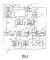
- FIG. 1is a block diagram of an eye protection device constructed in accordance with the present invention.
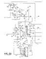
- FIG. 2is a schematic diagram of a control circuit constructed in accordance with the present invention for controlling a shutter assembly.
- FIG. 3is a graph illustrating a positive voltage signal and a negative voltage signal in accordance with the present invention.
- FIG. 4is a front perspective view of the eye protection device.
- FIG. 5is a rear perspective view of the eye protection device.
- FIG. 6is a rear elevational view of the eye protection device.
- FIG. 7is a side elevational view of the eye protection device.
- FIG. 8is a front elevational view of the eye protection device.
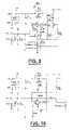
- FIG. 9is a second embodiment of a control circuit constructed in accordance with the present invention for controlling the shutter assembly.
- FIG. 10is a third embodiment of a control circuit constructed in accordance with the present invention for controlling the shutter assembly.
- the eye protection device 10is designed to automatically darken in the presence of an intense light, such as a welding arc.
- the eye protection device 10is preferably adapted to be worn by an individual.
- the eye protection device 10can be implemented in the form of a cassette 11 ( FIGS. 4-8 ) suitable for mounting in a welding helmet (not shown).
- the eye protection device 10is provided with a control circuit 12 , and a shutter assembly 14 .
- the shutter assembly 14is an auto-darkening filter capable of being driven between a clear state and a dark state. In the clear state, an individual can see through the shutter assembly 14 under ambient light conditions. In the dark state, the shutter assembly 14 becomes opaque so that the individual can only see through the shutter assembly 14 in the presence of an intense light, such as a welding arc.
- the switching speed of the eye protection device 10is an important performance attribute of the eye protection device 10 .
- the switching speedis the time period for switching the shutter assembly 14 from the clear state to the dark state.
- a dark state drive signal having a high voltage, e.g. 30 Vis provided to the shutter assembly 14 to enhance the switching speed of the shutter assembly 14 .
- the shutter assembly 14is preferably a liquid crystal display, such as a twisted nematic liquid crystal display.
- the control circuit 12senses the intense light and outputs the dark state drive signal to the shutter assembly 14 to cause the shutter assembly 14 to switch from the clear state to the dark state. If the control circuit 12 senses that no welding arc is present, the control circuit 12 will cause a “clear state” drive signal to be delivered to the shutter assembly 14 .
- control circuit 12is provided with a power supply 16 , a power regulation circuit 20 , a sensor circuit 24 , a weld detect circuit 28 , a positive voltage timer 32 , a negative voltage timer 36 , a positive voltage generator 40 , a negative voltage generator 44 , a shade control circuit 46 , a delay circuit 48 , an oscillator circuit 52 , and a delivery circuit 56 .
- the power supply 16includes a battery power supply 60 , and a solar power supply 64 .
- the solar power supply 64provides electrical power to the sensor circuit 24 via a power line 68 , and electrical power to the power regulation circuit 20 via a power line 72 .
- the battery power supply 60provides electrical power to the power regulation circuit 20 via a power line 74 .
- the power regulation circuit 20allows the solar power supply 64 to power the sensor circuit 24 , and regulates any additional power from the solar power supply 64 to be supplied to the remainder of the control circuit 12 .
- This additional poweris preferably regulated from above the voltage of the battery power supply 60 so that the power generated by the solar power supply 64 will be used before any power from the battery power supply 60 . This reduces the load on the battery power supply 60 and thereby extends the life of the battery power supply 60 .
- the solar cell voltage that assists the rest of the control circuit 12 (non-sensor)must be limited to a predetermined voltage, such as 6.4V.
- a predetermined voltagesuch as 6.4V.
- low current Zener diodesZ 1 and Z 2
- These Zener diodes (Z 1 and Z 2 )need a minimum of 4 uA to 8 uA for their reference voltage to be stable at 1.22V each. For this to happen, first if the eye protection unit 10 is in the clear state, the shade control circuit 46 is off and (if enough light is on the solar power supply 64 ) the current must come from the solar power supply 64 . This is done through R 14 . If there is not enough light the reference will not affect the shade.
- the second stateis if the eye protection unit 10 is in the dark state. In the dark state the reference must be accurate. Some solar power can be used, but to make sure the Zener diodes Z 1 and Z 2 have enough current through them, even at low light, additional current is supplied from the shade control circuit 46 through R 50 . This will insure the Zener diodes have enough current to maintain a stable voltage to the shade control circuit 46 via a line 75 and thus a stable shade.
- the regulation of the solar power supply 64can be implemented in other manners.
- an alternate circuit having a FETis utilized to regulate the solar power supply 64 to maintain the stable reference voltage.
- an op-amp circuitis utilized to regulate the solar power supply 64 to maintain the stable reference voltage.
- the battery power supply 60can be provided with any suitable voltage so as to supply power to the control circuit 12 and the shutter assembly 14 .
- the battery power supply 60can be provided with a voltage in a range from about 2.0 V to about 6.5 V. In a preferred embodiment depicted in FIG. 2 , the battery power supply 60 has about 6 Volts.
- the sensor circuit 24detects the presence of light and outputs a sensor output signal representative of the level of light detected.
- the sensor output signalis output to the weld detect circuit 28 via a signal path 76 .
- the weld detect circuit 28enables the drive signal that will be delivered to the shutter assembly 14 .
- the sensor output signalindicates to the weld detect circuit 28 that an intense light, such as a welding arc is present, the weld detect circuit 28 will cause a dark state drive signal to be delivered to the shutter assembly 14 .
- the weld detect circuit 28will cause a “clear state” drive signal to be delivered to the shutter assembly 14 .
- the dark state drive signalis provided with two components; a high voltage pulse followed by a stable AC waveform.
- the high voltage pulsequickly drives the shutter assembly 14 from the clear state to the dark state.
- the stable AC waveformmaintains the shutter assembly 14 in the dark state.
- the high voltage pulsepreferably has a voltage in a range from about 15 V to about 120 V, and a time period from about 10 microseconds to about 100 milliseconds. In general, the voltage of the high voltage pulse will depend on the maximum voltage ratings of the components utilized to implement the control circuit 12 . In one preferred embodiment, the voltage of the high voltage pulse is about 30 V, and the time period of the high voltage pulse is about 1 ms.
- the high voltage pulseis formed by a positive voltage signal (referenced to ground) synchronized with a negative voltage signal (referenced to ground).
- the positive and negative voltage signalsare labeled in FIG. 3 with the designations “PVS” and “NVS”. In other words, the leading edges of the positive voltage signal and the negative voltage signals are synchronized.
- the shutter assembly 14does not have a ground reference, and therefore, does not differentiate positive or negative. The voltage of the high voltage pulse in the dark state drive signal is thus the difference between the positive voltage signal and the negative voltage signal.
- the positive voltage signalis produced by the positive voltage timer 32 and the positive voltage generator 40 .
- the negative voltage signalis produced by the negative voltage timer 36 and the negative voltage generator 44 .
- the positive voltage timer 32sets the time period of the positive voltage signal.
- the positive voltage generator 40produces the magnitude of the positive voltage signal.
- the negative voltage timer 36sets the time period of the negative voltage signal.
- the negative voltage generator 44produces the magnitude of the negative voltage signal.
- the positive voltage generator 40triples the voltage of the battery power supply 60
- the negative voltage generator 44doubles the voltage of the battery power supply 60 so that the high voltage pulse has a voltage 5 times the voltage of the battery power supply 60 .
- the positive voltage timer 32receives electrical power (via a signal path 79 ) having the increased voltage from the positive voltage generator 40 so that the positive voltage timer 32 can switch components in the positive voltage generator.
- the advantage of using the positive voltage signal and the negative voltage signalis that the cost of manufacturing the control circuit 12 is reduced. That is, electrical components which switch over 18 Volts are more expensive than electrical components which switch below 18 Volts.
- the positive voltage signal and the negative voltage signalonly one more expensive and higher voltage part, i.e. the delivery circuit 56 , is needed to send a voltage higher than 18 Volts to the shutter assembly 14 .
- the weld detect circuit 28When the sensor output signal indicates to the weld detect circuit 28 that an intense light, such as a welding arc is present, the weld detect circuit 28 outputs a signal to the positive voltage timer 32 and the negative voltage timer 36 via signal paths 80 and 84 to cause the positive voltage signal and the negative voltage signal to be fed to the delivery circuit 56 via signal paths 88 and 92 . That is, upon receipt of the signal from the weld detect circuit 28 , the positive voltage timer 32 and the negative voltage timer 36 output respective timing signals to the positive voltage generator 40 and the negative voltage generator 44 via signal paths 96 and 100 . In response thereto, the positive voltage generator 40 and the negative voltage generator 44 output the positive voltage signal and the negative voltage signal to the delivery circuit 56 .
- the delivery circuit 56outputs the positive voltage signal to the shutter assembly 14 on a signal path 104 , and the negative voltage signal to the shutter assembly 14 on a signal path 108 to cause the shutter assembly 14 to switch from the clear state to the dark state.
- the weld detect circuit 28outputs a signal to the delivery circuit 56 via the delay circuit 48 and signal paths 112 and 116 to cause the delivery circuit 56 to enable the stable AC waveform to the shutter assembly 14 .
- the stable AC waveformmaintains the shutter assembly 14 in the dark state.
- the stable AC waveformmaintains the shutter assembly 14 in the dark state.
- the stable AC waveformis preferably a squarewave having a user adjustable magnitude varying from a maximum of about +3.2 V-4 V to a minimum of about ⁇ 3.2V- ⁇ 4 V.
- the stable AC waveformcan be provided with other shapes, such as a sinusoidal shape, however, the efficiency of the circuit 12 will be reduced.
- the stable AC waveformis produced as follows.
- the shade control circuit 46provides a stable DC voltage signal having a magnitude sufficient to maintain the shutter assembly 14 in the dark state to the delivery circuit 56 via a signal path 120 .
- the oscillator circuit 52provides an oscillating signal to the delivery circuit 56 via a signal path 124 to cause the delivery circuit 56 to produce the stable AC waveform.
- the oscillating signalcauses the delivery circuit 56 to periodically switch the polarity of the signal transmitted to the shutter assembly 14 .
- the weld detect circuit 28will cause a “clear state” drive signal to be delivered to the shutter assembly 14 via the delay circuit 48 , the delivery circuit 56 and the signal paths 112 , 116 , 104 and 108 .
- the delay circuit 48delays the submission of the clear state drive signal to the delivery circuit 56 for a predetermined time, thus preventing the shutter assembly 14 from switching to a clear state during brief “off” periods in the weld pulsations that exist with various weld types. Further, once the welding arc is extinguished, the work piece which is being welded may glow brightly for several milliseconds thereafter.
- the delay circuit 48delays the clear state drive signal for desirably between about 0.1 seconds to about 1 seconds, and more desirably between about 0.2 seconds to about 0.4 seconds so as to protect the individual's eyes from the glow from the work piece.
- the delay circuit 48may have a fixed time delay, or may be adjustable by a user so as to be set based on the user's preference.
- the weld detect circuit 28switches power to the oscillator circuit 52 and the shade control circuit 46 via a signal path P 1 to conserve battery power. That is, in the preferred embodiment, the oscillator circuit 52 and the weld detect circuit 28 are only enabled when the weld detect circuit 28 senses the welding arc.
- FIG. 2Shown in FIG. 2 is a schematic diagram of one preferred implementation of the control circuit 12 .
- the sensor circuit 24 of the eye protection device 10includes a pair of spatially disposed light detectors, such as phototransistors D 10 and D 11 , for sensing the welding arc.
- the eye protection device 10can be provided with a plurality of controls for controlling various settings thereof.
- the eye protection device 10can be provided with a first knob 200 and a second knob 202 for adjusting the sensitivity and the shade of the eye protection device 10 .
- the first and second knobs 200 and 202can be connected to any suitable component for adjusting the settings of the eye protection device 10 .
- the first and second knobs 200 and 202can be connected to potentiometers.
- FIG. 5is a rear perspective view of the eye protection device.
- the sensor circuit 24includes one or more phototransistor D 10 and D 11 with the output of each phototransistor D 10 and D 11 coupled to feedback circuits 206 a and 206 b.
- the construction and function of the phototransistors D 10 and D 11are similar.
- the feedback circuits 206 a and 206 bare similar. Thus, only the phototransistor D 10 and the feedback circuit 206 a will be discussed hereinafter for purposes of brevity.
- the output of phototransistor D 10is sent to line 208 .
- a load resistor R 40is connected between line 208 and ground. Additionally, a capacitor C 8 couples line 208 to line 209 .
- Resistor R 10is connected between line 208 and ground.
- Line 209is also connected to the noninverting input of amplifier 210 .
- Amplifier 210is preferably configured as closed loop noninverting amplifier wherein the resistors R 34 , R 33 , R 44 and R 21 form an adjustable feedback loop connected to the inverting input of amplifier 210 as shown. In particular, R 21 is adjustable to permit the sensitivity of the sensor circuit 24 to be adjusted.
- the output of amplifier 210 on line 76serves as the sensor circuit output. Line 76 is connected to the input of the weld detect circuit 28 .
- the solar power supply 64powers the phototransistor D 10 and amplifier 210 via line 68 .
- phototransistor D 10 and amplifier 210will not receive power, thus preventing the phototransistor D 10 and amplifier 210 from draining the battery power supply 60 when the welding helmet is not in use (when not in use, the welding helmet is typically not exposed to intense light).
- the feedback circuit 206 a for the phototransistor D 10comprises a resistor capacitor circuit 216 connected between the emitter of the phototransistor and ground, and a feedback transistor Q 5 having a base coupled to line 218 of the resistor capacitor circuit 216 , a collector coupled to the base of the phototransistor D 10 , and an emitter coupled to the ground via resistor R 42 .
- Phototransistor D 10serves as the weld sensor. It receives an input of incident light 220 and produces an output on line 208 representative of the intensity of the incident light.
- the phototransistor D 10 used in the present inventionis preferably a planar phototransistor configured for a surface mount.
- the planar phototransistoris smaller than conventional metal can phototransistors, thus allowing a reduction in size of the unit in which the sensor circuit is implemented. While the metal can phototransistors used in the sensor circuits of the prior art had a thickness of about 1 ⁇ 2 inch, the planar phototransistors with a surface mount used in the present invention have a thickness of only about 1 ⁇ 4 inch. This reduction is thickness allows the sensor circuit to be implemented into a smaller and sleeker unit.
- the surface mount configuration of the phototransistor D 10allows the phototransistor to be easily affixed to a circuit board.
- the inventor hereinhas found that the TEMT4700 silicon npn phototransistor manufactured by Vishay-Telefunken is an excellent phototransistor for the present invention as it has a smaller size than conventional metal can phototransistors and allows the sensor circuit to maintain a constant signal level without excessive loading or the drawing of excessive current.
- the resistor capacitor circuit 216 and the feedback transistor Q 5 in the phototransistor feedback circuit 206 afunction to adjust the sensitivity of the phototransistor D 10 .
- the resistors R 30 and R 8 and capacitor C 15are chosen to be of a size to provide a relatively large time constant, and therefore a relatively slow response to changes in voltage on line 208 .
- the delayexists because of the time it takes for the voltage on line 218 to charge to an amount sufficiently large to activate Q 5 .
- Exemplary values for R 30 and R 8are 1 M ⁇ and 2 M ⁇ respectively.
- An exemplary value for C 15is 0.1 ⁇ F.
- the signal on line 208if fed into the amplifier 210 .
- the signalis first passed through a high pass circuit formed by capacitors C 8 and C 9 to block the DC component of the detected signal.
- Line 209contains the DC blocked detected signal.
- the current on line 209is diverted to ground via resistor R 10 .
- the sensor circuit 24operates in the presence of both AC welds and DC welds.
- an AC weldalso known as a MIG weld
- the welding lightis pulsating.
- the phototransistor D 10will detect a pulsating light signal.
- the frequency of the pulsationsis often 120 Hz.
- a DC weldalso known as a TIG weld
- the welding lightis substantially continuous, with the exception of a small AC component.
- the phototransistorwill produce a pulsating output on line 208 .
- the variations in the voltage signal due to the pulseswill be passed through the capacitors C 8 and C 9 to line 209 and fed into the amplifier 210 .
- the amplifier 210will then provide gain for the signal on line 209 which is sufficient to trigger the delivery of the “dark state” drive signal to the shutter assembly 14 .
- the phototransistor D 10When a DC weld is present, the phototransistor D 10 will quickly produce an output on line 208 catching the rising edge of the DC weld. This sudden rise in voltage on line 208 will be passed through to the amplifier 210 causing a signal on line 76 sufficient to trigger the delivery of a “dark state” drive signal to the shutter assembly 400 . Thereafter, capacitors C 8 and C 9 will block the DC component of the DC weld, allowing only the AC variations in the DC weld to pass through to the amplifier 210 .
- a non-reactive elemente.g., resistor R 49 , is positioned in parallel with the high-pass filter circuit formed by the capacitors C 8 and C 9 .
- the non-reactive elementprovides a DC bias to the input of the amplifier 210 to aid in the detection of the DC weld. That is, the brighter the light being generated from the weld becomes, the more sensitive the sensor circuit 24 becomes.
- R 49can have a value of 10 M ohm.
- the amplifier 210can be a closed loop, noninverting amplifier as described above.
- the amplifier 210can be provided with a feed-back loop formed by R 34 , R 33 , R 44 and R 21 .
- R 21is preferably an adjustable resistor so that the gain of the amplifier 210 and thus the sensitivity of the sensor circuit 24 , can be adjusted by the user. Suitable values for R 34 , R 33 , R 44 and R 21 have been found to be 1 M ohm, 2 M ohm, 392 k ohm and 1 M ohm.
- the sensor circuit 24is also provided with an OR logical circuit 224 receiving the outputs from the circuits 206 a and 206 b.
- the OR logical circuit 224permits the highest voltage level from the circuits 206 a and 206 b to be passed.
- the output of the amplifier 210is fed into the weld detect circuit 28 .
- the weld detect circuit 28is provided with an electronic switch, an example of which is shown in FIG. 2 as the FET Q 9 , a delay circuit 230 and a switching circuit 232 .
- the delay circuit 230can be formed of a RC circuit and serves to prevent inadvertent switching of the shutter assembly 14 from the dark state to the clear state. That is, the light received by the sensor circuit 24 from the welding arc can be a pulsating signal caused by sputtering of the weld.
- the amplifier 210receives a signal of sufficient magnitude, the output of the amplifier 210 goes high. The high signal is fed to the gate of the FET Q 9 . FET Q 9 then turns on and thereby shorts a capacitor C 10 to ground. Once the intensity of the light detected by the sensor circuit 24 decreases, capacitor C 10 will begin charging through R 26 until the next pulse of intense light is provided to the sensor circuit 24 .
- the time period of the RC circuit formed by the capacitor C 10 and a resistor R 26is selected to maintain the capacitor C 10 in a “low” state between pulses to maintain a stable low signal to the switching circuit 232 .
- the “low” signalis provided to a switch input “C” of the switching circuit 232 .
- Thiscauses the switching circuit 232 to switch between the Z 1 and the Z 0 inputs.
- a high signalis applied to the Z 0 input and the ground reference is applied to the Z 1 input.
- the delay circuit 48is provided with an electronic switch as represented by transistor Q 8 , and an RC circuit as represented by R 38 and C 13 . The high signal switches on the transistor Q 8 causing the capacitor C 13 to charge.
- the delay circuit 48provides a time delay when the control circuit 12 switches from the dark state to the clear state. That is, when the welding stops the workpiece is still glowing brightly.
- the time delay of the delay circuit 48is selected such that the user's eyes will be protected until the glow of the workpiece is diminished.
- the time delay of the delay circuit 48can vary widely based on user preference. However, suitable time periods range from about 0.2 seconds to about 0.4 seconds. Suitable values for the resistor R 38 and the capacitor C 13 are 4.3 M ohm and 0.047 micro farads.
- the positive voltage timer 32is formed by resistors R 23 , R 48 , transistor Q 10 and capacitor C 20 .
- the negative voltage timer 36is formed by resistors R 28 , R 35 , transistor Q 7 and capacitor C 11 .
- the positive and negative voltage timers 32 and 36serve to properly bias the inputs of the positive and negative voltage generators 40 and 44 to generate the high voltage pulse.
- the emitter of the transistor Q 8is connected to the capacitor C 12 via the line 116 .
- the capacitor C 12is connected to the base of transistors Q 7 and Q 10 .
- the transistors Q 7 and Q 10short the capacitors C 11 and C 20 , which then have to recharge causing the time frame in which the positive and negative voltage generators 40 and 44 produce the high voltage pulse. This also causes low signals to be provided to switching circuits U 4 and U 5 via lines 96 and 100 .
- the positive voltage generator 40is also provided with at least two capacitors C 2 and C 3 , and a directional control circuit 244 .
- the switching circuit U 4has a plurality of switches X, Y and Z for switching the positive voltage generator between a charging state and a discharging state.
- Each of the capacitors C 2 and C 3are connected to the switching circuit U 4 and a reference voltage to establish charging of the capacitors C 2 and C 3 in the charging state of the switching circuit U 4 .
- the all of the switches of the switching circuit U 4switch to the discharging state.
- the capacitors C 2 and C 3are stacked to sum the voltage accumulated on the capacitors. That is, a positive lead of the capacitor C 2 is connected to a negative lead of the capacitor C 3 through the switch X. Assuming that the voltage reference is 6 V, this would cause a 12 V potential to exist across the stacked capacitors C 2 and C 3 . Further, the negative lead of the capacitor C 2 is connected to the reference voltage, e.g., 6 V, through the switch Y so that the positive voltage signal, e.g., +18 V, exists from the ground reference to the positive lead of the capacitor C 3 .
- the directional control circuit 244permits the flow of current between the negative leads of the capacitors C 2 and C 3 and the reference voltage in the charging state of the switching circuit U 4 , and prevents the flow of current between the negative leads of the capacitors C 2 and C 3 in the discharging state of the switching circuit U 4 so that the positive voltage signal is generated.
- the positive voltage signalis then provided to the delivery circuit 56 via lines 248 and 88 through the switch Z.
- the directional control circuit 244includes at least two diodes, as designated by the reference numeral D 2 .
- D 2the directional control circuit 244 has been shown and described as the diodes D 2 , it should be understood that the directional control circuit 244 could be implemented in other manners.
- the directional control circuit 244can be implemented as any device having a P-N junction, such as a transistor, or an enhanced MOSFET.
- capacitors C 2 and C 3can vary widely depending on the 1) output voltage, 2) load, and 3) length of time for the voltage to switch the shutter assembly 14 .
- the capacitors C 2 and C 3can be 2.2 micro farad capacitors.
- the switching circuit U 4is preferably 1) an integrated circuit having a plurality of electronically controlled switches, or 2) separate electronically controlled switches.
- the negative voltage generator 44is constructed in a similar manner as the positive voltage generator 40 , except as discussed hereinafter.
- the negative voltage generator 44is provided with a directional control circuit 250 permitting the flow of current between the negative leads of the capacitors C 4 and C 5 and the reference voltage in the charging state of the switching circuit U 5 , and preventing the flow of current between the negative leads of the capacitors and the reference voltage in the discharging state of the switching circuit U 5 .
- the positive lead of the capacitor C 4is connected to ground in the discharging state of the switching circuit such that the negative voltage signal is produced between the ground reference and the negative lead of the capacitor C 5 .
- the negative voltage signalis output to the delivery circuit 56 through switch Z of switching circuit U 5 via lines 252 and 92 .
- a high signalis output to the positive and negative voltage generators 40 and 44 via the lines 96 and 100 .
- the high signalswitches the switching circuits U 4 and U 5 from the discharging state to the charging state to turn off the positive and negative voltage signals.
- a voltage signalis transmitted to the delivery circuit 56 from the shade control 46 through switch X of switching circuit U 3 and via lines 256 , 120 and 88 to provide the stable AC waveform as discussed above.
- the weld detect circuit 28switches power to the oscillator circuit 52 and the shade control circuit 46 via a signal path P 1 to conserve battery power. That is, in the preferred embodiment, the oscillator circuit 52 and the shade control circuit 46 are only enabled when the weld detect circuit 28 senses the welding arc.
- the “B” input of the switching circuit 232 of the weld detect circuit 28receives a signal on the line 116 when the high signal from the Z output of the switching circuit 232 switches on the transistor Q 8 causing the capacitor C 13 to charge.
- the signal on the line 116switches to a “low” state thereby turning off the transistor Q 8 .
- Thispermits the capacitor C 13 to discharge through the resistor R 38 causing a low state signal to be delivered on the line 116 after a predetermined time period.
- the low state signalis received by the “A” and “B” inputs of the switching circuit 232 and thereby causes a “low” state signal to be output by the “X” and “Y” outputs. This causes the shutter assembly 14 to switch from the dark state to the clear state and also disables power to the shade control circuit 46 and the oscillator circuit 52 to conserve battery power.
- the power regulation circuit 20allows the solar power supply 64 to power the sensor circuit 24 , and regulates any additional power from the solar power supply 64 to be supplied to the remainder of the control circuit 12 .
- This additional poweris preferably regulated from above the voltage of the battery power supply 60 so that the power generated by the solar power supply 64 will be used before any power from the battery power supply 60 . This reduces the load on the battery power supply 60 and thereby extends the life of the battery power supply 60 .
- the shutter assembly 14 and the control circuit 12can be implemented in a cassette connectable to a welding helmet, or integrated into the welding helmet.
- the user controlscan be on the cassette or separate from the cassette.
- the user controlscan be implemented as a “pig-tail.”
Landscapes
- Physics & Mathematics (AREA)
- General Physics & Mathematics (AREA)
- Spectroscopy & Molecular Physics (AREA)
- Health & Medical Sciences (AREA)
- Ophthalmology & Optometry (AREA)
- Engineering & Computer Science (AREA)
- Biomedical Technology (AREA)
- Heart & Thoracic Surgery (AREA)
- Vascular Medicine (AREA)
- Life Sciences & Earth Sciences (AREA)
- Animal Behavior & Ethology (AREA)
- General Health & Medical Sciences (AREA)
- Public Health (AREA)
- Veterinary Medicine (AREA)
- Arc Welding Control (AREA)
Abstract
Description
Claims (7)
Priority Applications (1)
| Application Number | Priority Date | Filing Date | Title |
|---|---|---|---|
| US11/707,298US7659495B2 (en) | 2001-05-05 | 2007-02-19 | Auto darkening eye protection device having a regulated solar power supply |
Applications Claiming Priority (4)
| Application Number | Priority Date | Filing Date | Title |
|---|---|---|---|
| US28876001P | 2001-05-05 | 2001-05-05 | |
| US10/139,837US6841772B1 (en) | 2001-05-05 | 2002-05-03 | Eye-protection device having dual high voltage switching |
| US11/035,805US7180047B2 (en) | 2001-05-05 | 2005-01-10 | Eye-protection device having dual high voltage switching |
| US11/707,298US7659495B2 (en) | 2001-05-05 | 2007-02-19 | Auto darkening eye protection device having a regulated solar power supply |
Related Parent Applications (1)
| Application Number | Title | Priority Date | Filing Date |
|---|---|---|---|
| US11/035,805DivisionUS7180047B2 (en) | 2001-05-05 | 2005-01-10 | Eye-protection device having dual high voltage switching |
Publications (2)
| Publication Number | Publication Date |
|---|---|
| US20070145234A1 US20070145234A1 (en) | 2007-06-28 |
| US7659495B2true US7659495B2 (en) | 2010-02-09 |
Family
ID=33554733
Family Applications (3)
| Application Number | Title | Priority Date | Filing Date |
|---|---|---|---|
| US10/139,837Expired - LifetimeUS6841772B1 (en) | 2001-05-05 | 2002-05-03 | Eye-protection device having dual high voltage switching |
| US11/035,805Expired - LifetimeUS7180047B2 (en) | 2001-05-05 | 2005-01-10 | Eye-protection device having dual high voltage switching |
| US11/707,298Expired - Fee RelatedUS7659495B2 (en) | 2001-05-05 | 2007-02-19 | Auto darkening eye protection device having a regulated solar power supply |
Family Applications Before (2)
| Application Number | Title | Priority Date | Filing Date |
|---|---|---|---|
| US10/139,837Expired - LifetimeUS6841772B1 (en) | 2001-05-05 | 2002-05-03 | Eye-protection device having dual high voltage switching |
| US11/035,805Expired - LifetimeUS7180047B2 (en) | 2001-05-05 | 2005-01-10 | Eye-protection device having dual high voltage switching |
Country Status (1)
| Country | Link |
|---|---|
| US (3) | US6841772B1 (en) |
Cited By (3)
| Publication number | Priority date | Publication date | Assignee | Title |
|---|---|---|---|---|
| US20090276931A1 (en)* | 2003-08-11 | 2009-11-12 | Hamilton Thomas J | Eye-Protection Device Having Dual High Voltage Switching |
| US20140001343A1 (en)* | 2011-03-18 | 2014-01-02 | Otos Wing Co., Ltd. | Antiglare apparatus having a self-diagnosis mode |
| US20140021337A1 (en)* | 2011-04-14 | 2014-01-23 | Otos Wing Co., Ltd. | Multifunctional digital antiglare device |
Families Citing this family (10)
| Publication number | Priority date | Publication date | Assignee | Title |
|---|---|---|---|---|
| US6881939B1 (en) | 2001-05-05 | 2005-04-19 | Jackson Products, Inc. | Microprocessor based automatically dimmable eye protection device |
| WO2005002480A1 (en)* | 2003-07-03 | 2005-01-13 | Lightswitch Safety Systems, Inc. | Multi-stage sensor for an auto-darkening lens for use in welding and method |
| JP4297103B2 (en)* | 2005-02-17 | 2009-07-15 | セイコーエプソン株式会社 | ELECTRO-OPTICAL DEVICE, MANUFACTURING METHOD THEREOF, AND ELECTRONIC DEVICE |
| US7812279B2 (en)* | 2006-03-23 | 2010-10-12 | Monzyk Doug J | Welding flash protection apparatus |
| US9519158B2 (en)* | 2013-10-10 | 2016-12-13 | John Jason Brudz | Tactical lighting unit with synchronized eye protection |
| US10251786B2 (en)* | 2013-11-21 | 2019-04-09 | Optrel Holding AG | Method and apparatus for controlling opening of an auto-darkening filter in an eye protection device |
| CN104682867B (en)* | 2014-12-30 | 2023-07-28 | 宁夏小牛自动化设备股份有限公司 | Welding detection method and detection equipment for crystalline silicon solar cell |
| CN106419346A (en)* | 2016-11-07 | 2017-02-22 | 四川唯诺家私有限公司 | Folding screen with eye health-care function |
| CN110974536B (en)* | 2019-12-30 | 2022-02-22 | 江苏江翔光电科技有限公司 | Control circuit of automatic light-changing welding mask |
| FI129978B (en)* | 2020-10-19 | 2022-12-15 | Kemppi Oy | Auto-darkening lcd filter glass element |
Citations (67)
| Publication number | Priority date | Publication date | Assignee | Title |
|---|---|---|---|---|
| GB325586A (en) | 1928-11-22 | 1930-02-24 | British Thomson Houston Co Ltd | Improvements relating to devices for protecting a person from the radiations of an electric arc |
| US2423320A (en) | 1944-07-29 | 1947-07-01 | Jr Samuel C Hurley | Welder's helmet |
| US2548230A (en) | 1946-06-27 | 1951-04-10 | Molyneux & Aspinwall Inc | Welding mask |
| US2761046A (en) | 1953-02-16 | 1956-08-28 | Herrick James Elder | Automatic arc welding viewing mechanism |
| US3137784A (en) | 1961-02-27 | 1964-06-16 | Kasemann Erwin | Device for protecting the eyes of welders |
| US3159844A (en) | 1962-11-09 | 1964-12-08 | Samuel C Halpert | Electromagnetically controlled hood device for welding and cutting |
| US3245315A (en) | 1962-09-05 | 1966-04-12 | Alvin M Marks | Electro-optic responsive flashblindness controlling device |
| US3575491A (en) | 1968-10-16 | 1971-04-20 | Rca Corp | Decreasing response time of liquid crystals |
| US3731986A (en) | 1971-04-22 | 1973-05-08 | Int Liquid Xtal Co | Display devices utilizing liquid crystal light modulation |
| DE2315308A1 (en) | 1972-03-27 | 1973-10-11 | Aga Ab | DEVICE FOR PROTECTING THE HUMAN EYE AGAINST RADIATION |
| US3873804A (en) | 1972-04-14 | 1975-03-25 | Mack Gordon | Welding helmet with eye piece control |
| US3881808A (en) | 1973-12-07 | 1975-05-06 | Motorola Inc | Liquid crystal light control device having a high transmission efficiency |
| US3881809A (en) | 1972-03-10 | 1975-05-06 | Hoffmann La Roche | Reflection system for liquid crystal displays |
| US3890628A (en) | 1973-10-23 | 1975-06-17 | Motorola Inc | Liquid crystal light control device and circuit |
| US3918796A (en) | 1971-02-09 | 1975-11-11 | Hoffmann La Roche | Liquid-crystal non-linear light modulators using electric and magnetic fields |
| US3967881A (en) | 1974-04-04 | 1976-07-06 | Matsushita Electric Industrial Co., Ltd. | Liquid crystal display |
| US4039803A (en) | 1976-04-08 | 1977-08-02 | Mack Gordon | Electro-optic welding helmet lens assembly |
| SE7608690L (en) | 1975-03-07 | 1978-02-04 | Hornell Ake | OPTICAL FILTER |
| US4071912A (en) | 1974-12-02 | 1978-02-07 | Revue Thommen Ag | Light filter for welder's mask |
| USRE29684E (en) | 1973-12-26 | 1978-06-27 | Welding helmet with eye piece control | |
| US4155122A (en) | 1975-12-02 | 1979-05-22 | Revue Thommen Ag | Light shield for welder's mask |
| US4237557A (en) | 1979-07-30 | 1980-12-09 | Mack Gordon | Control system for welding helmet liquid crystal light shutter |
| US4240709A (en) | 1978-04-24 | 1980-12-23 | Esab Aktiebolag | Multiple layer protective glass, particularly a protective glass for a welding shield |
| US4279474A (en) | 1980-03-25 | 1981-07-21 | Belgorod Barry M | Spectacle lens having continuously variable controlled density and fast response time |
| US4328490A (en) | 1979-06-29 | 1982-05-04 | Tokyo Shibaura Denki Kabushiki Kaisha | Liquid crystal display device with low battery indication |
| US4385806A (en) | 1978-06-08 | 1983-05-31 | Fergason James L | Liquid crystal display with improved angle of view and response times |
| FR2530039A1 (en) | 1982-07-06 | 1984-01-13 | Cuvelier Antoine | Safety (protective) glasses having automatically adjustable transmission using liquid crystals |
| US4435047A (en) | 1981-09-16 | 1984-03-06 | Manchester R & D Partnership | Encapsulated liquid crystal and method |
| US4436376A (en) | 1980-02-13 | 1984-03-13 | Fergason James L | Light modulator, demodulator and method of communication employing the same |
| JPS5992276A (en) | 1982-11-17 | 1984-05-28 | 川崎重工業株式会社 | Motorcycle cowling mounting structure |
| JPS59111102A (en) | 1982-12-16 | 1984-06-27 | Nippon Denso Co Ltd | Glare shielding type reflecting mirror |
| US4540243A (en) | 1981-02-17 | 1985-09-10 | Fergason James L | Method and apparatus for converting phase-modulated light to amplitude-modulated light and communication method and apparatus employing the same |
| EP0157744A1 (en) | 1984-02-24 | 1985-10-09 | Peter Toth | Optical filter for protective welding lens assemblies |
| US4556289A (en) | 1983-03-21 | 1985-12-03 | Manchester R & D Partnership | Low birefringence encapsulated liquid crystal and optical shutter using same |
| US4560239A (en) | 1984-02-29 | 1985-12-24 | Amnon Katz | Liquid crystal active light shield |
| US4582396A (en) | 1983-05-09 | 1986-04-15 | Tektronix, Inc. | Field sequential color display system using optical retardation |
| USRE32521E (en) | 1978-06-08 | 1987-10-13 | Fergason James L | Light demodulator and method of communication employing the same |
| US4710694A (en) | 1986-06-02 | 1987-12-01 | Acme Electric Corporation | Microprocessor controlled battery charger |
| US4759608A (en) | 1985-12-31 | 1988-07-26 | Yang Jong P | Automatic liquid crystal light-shutter |
| US4785226A (en)* | 1985-10-21 | 1988-11-15 | Casio Computer Co., Ltd. | Powder supply device with solar cell |
| US4813766A (en) | 1988-03-02 | 1989-03-21 | Raytheon Company | Optical time delay apparatus |
| US4821292A (en) | 1987-06-03 | 1989-04-11 | General Electric Company | Adaptive limiter/detector which changes time constant upon detection of dotting pattern |
| US4863244A (en) | 1988-03-11 | 1989-09-05 | Optrel Ag | Electro-optic welding lens assembly |
| EP0335056A1 (en) | 1986-10-09 | 1989-10-04 | Optrel Ag | Light filter with automatic optical transmission control |
| US4877310A (en) | 1988-08-04 | 1989-10-31 | Xerox Corporation | Electronically variable MTF filter for image sensor arrays |
| EP0349665A1 (en) | 1988-07-07 | 1990-01-10 | Optrel Ag | An electro-optic welding lens assembly |
| US4901074A (en) | 1987-12-31 | 1990-02-13 | Whirlpool Corporation | Glass membrane keyboard switch assembly for domestic appliance |
| US4928181A (en) | 1988-11-21 | 1990-05-22 | Philip Morris Incorporated | Methods and apparatus for optically enhancing selected features in an input image |
| WO1990014809A1 (en) | 1989-06-05 | 1990-12-13 | Hörnell Elektrooptik Ab | A welder's helmet |
| US5015086A (en) | 1989-04-17 | 1991-05-14 | Seiko Epson Corporation | Electronic sunglasses |
| US5074647A (en) | 1989-12-07 | 1991-12-24 | Optical Shields, Inc. | Liquid crystal lens assembly for eye protection |
| US5113270A (en) | 1988-10-19 | 1992-05-12 | Fergason James L | Variable density light control apparatus |
| US5184156A (en) | 1991-11-12 | 1993-02-02 | Reliant Laser Corporation | Glasses with color-switchable, multi-layered lenses |
| US5208688A (en) | 1991-02-08 | 1993-05-04 | Osd Envizion Company | Eye protection device for welding helmets |
| US5248880A (en) | 1991-03-25 | 1993-09-28 | Osd Envizion Company | Detector system for detecting the occurrence of welding |
| US5252817A (en) | 1991-03-25 | 1993-10-12 | Osd Envizion Company | Detector system for detecting the occurrence of welding using detector feedback |
| US5347383A (en) | 1989-06-12 | 1994-09-13 | Osd Envizion Company | High speed, low power driving circuit for liquid crystal shutter |
| US5377032A (en) | 1993-02-05 | 1994-12-27 | Osd Envizion Company | Electro-optic light shutter and frame assembly with integrated switching mechanism |
| US5420502A (en) | 1992-12-21 | 1995-05-30 | Schweitzer, Jr.; Edmund O. | Fault indicator with optically-isolated remote readout circuit |
| US5519522A (en) | 1993-08-11 | 1996-05-21 | Fergason; Jeffrey K. | Eye protection device for welding helmets and the like with hot mirror and indium tin oxide layer |
| US5671035A (en) | 1995-06-07 | 1997-09-23 | Barnes; Elwood E. | Light intensity reduction apparatus and method |
| US5751258A (en) | 1991-03-25 | 1998-05-12 | Osd Envizion, Inc. | Liquid crystal lens driver electronics for eye protection, high speed shuttering with consistent performance |
| WO1998057606A1 (en)* | 1997-06-18 | 1998-12-23 | Optrel Ag | Active electrooptic filter device |
| US6067129A (en) | 1996-03-15 | 2000-05-23 | Osd Envizion, Inc. | Welding lens with integrated display and method |
| US6070264A (en) | 1999-04-09 | 2000-06-06 | Jackson Products, Inc. | Welding helmet having auto-darkening and manually adjustable lens shade control |
| US6552316B1 (en) | 1998-12-29 | 2003-04-22 | Otos Co., Ltd. | Glare protecting device utilizing both optical and non-optical detectors and method of controlling thereof |
| US6614409B1 (en) | 1999-11-23 | 2003-09-02 | Otos Co., Ltd. | Glare shielding device of welding helmet and method of controlling the same |
Family Cites Families (5)
| Publication number | Priority date | Publication date | Assignee | Title |
|---|---|---|---|---|
| US29684A (en)* | 1860-08-21 | Coupling for belts | ||
| US32521A (en)* | 1861-06-11 | W S Kirkham | Lock and knob-latch | |
| US2761048A (en) | 1953-06-25 | 1956-08-28 | Ohio Crankshaft Co | High-frequency inductor |
| CA1021078A (en) | 1972-09-19 | 1977-11-15 | Sharp Kabushiki Kaisha | Drive system for liquid crystal display units |
| FR2451097A1 (en)* | 1979-02-07 | 1980-10-03 | Terasaki Denki Sangyo Kk | ELECTRIC AIR CIRCUIT SWITCH, MECHANISM AND HOUSING |
- 2002
- 2002-05-03USUS10/139,837patent/US6841772B1/ennot_activeExpired - Lifetime
- 2005
- 2005-01-10USUS11/035,805patent/US7180047B2/ennot_activeExpired - Lifetime
- 2007
- 2007-02-19USUS11/707,298patent/US7659495B2/ennot_activeExpired - Fee Related
Patent Citations (72)
| Publication number | Priority date | Publication date | Assignee | Title |
|---|---|---|---|---|
| GB325586A (en) | 1928-11-22 | 1930-02-24 | British Thomson Houston Co Ltd | Improvements relating to devices for protecting a person from the radiations of an electric arc |
| US2423320A (en) | 1944-07-29 | 1947-07-01 | Jr Samuel C Hurley | Welder's helmet |
| US2548230A (en) | 1946-06-27 | 1951-04-10 | Molyneux & Aspinwall Inc | Welding mask |
| US2761046A (en) | 1953-02-16 | 1956-08-28 | Herrick James Elder | Automatic arc welding viewing mechanism |
| US3137784A (en) | 1961-02-27 | 1964-06-16 | Kasemann Erwin | Device for protecting the eyes of welders |
| US3245315A (en) | 1962-09-05 | 1966-04-12 | Alvin M Marks | Electro-optic responsive flashblindness controlling device |
| US3159844A (en) | 1962-11-09 | 1964-12-08 | Samuel C Halpert | Electromagnetically controlled hood device for welding and cutting |
| US3575491A (en) | 1968-10-16 | 1971-04-20 | Rca Corp | Decreasing response time of liquid crystals |
| US3918796A (en) | 1971-02-09 | 1975-11-11 | Hoffmann La Roche | Liquid-crystal non-linear light modulators using electric and magnetic fields |
| US3731986A (en) | 1971-04-22 | 1973-05-08 | Int Liquid Xtal Co | Display devices utilizing liquid crystal light modulation |
| US3881809A (en) | 1972-03-10 | 1975-05-06 | Hoffmann La Roche | Reflection system for liquid crystal displays |
| DE2315308A1 (en) | 1972-03-27 | 1973-10-11 | Aga Ab | DEVICE FOR PROTECTING THE HUMAN EYE AGAINST RADIATION |
| US3873804A (en) | 1972-04-14 | 1975-03-25 | Mack Gordon | Welding helmet with eye piece control |
| US3890628A (en) | 1973-10-23 | 1975-06-17 | Motorola Inc | Liquid crystal light control device and circuit |
| US3881808A (en) | 1973-12-07 | 1975-05-06 | Motorola Inc | Liquid crystal light control device having a high transmission efficiency |
| USRE29684E (en) | 1973-12-26 | 1978-06-27 | Welding helmet with eye piece control | |
| US3967881A (en) | 1974-04-04 | 1976-07-06 | Matsushita Electric Industrial Co., Ltd. | Liquid crystal display |
| US4071912A (en) | 1974-12-02 | 1978-02-07 | Revue Thommen Ag | Light filter for welder's mask |
| SE7608690L (en) | 1975-03-07 | 1978-02-04 | Hornell Ake | OPTICAL FILTER |
| US4155122A (en) | 1975-12-02 | 1979-05-22 | Revue Thommen Ag | Light shield for welder's mask |
| US4039803A (en) | 1976-04-08 | 1977-08-02 | Mack Gordon | Electro-optic welding helmet lens assembly |
| US4240709A (en) | 1978-04-24 | 1980-12-23 | Esab Aktiebolag | Multiple layer protective glass, particularly a protective glass for a welding shield |
| US4385806A (en) | 1978-06-08 | 1983-05-31 | Fergason James L | Liquid crystal display with improved angle of view and response times |
| USRE32521E (en) | 1978-06-08 | 1987-10-13 | Fergason James L | Light demodulator and method of communication employing the same |
| USRE32521F1 (en) | 1978-06-08 | 1990-09-18 | James L Fergason | Light modulator demodulator and method of communication employing the same |
| US4328490A (en) | 1979-06-29 | 1982-05-04 | Tokyo Shibaura Denki Kabushiki Kaisha | Liquid crystal display device with low battery indication |
| US4237557A (en) | 1979-07-30 | 1980-12-09 | Mack Gordon | Control system for welding helmet liquid crystal light shutter |
| US4436376A (en) | 1980-02-13 | 1984-03-13 | Fergason James L | Light modulator, demodulator and method of communication employing the same |
| US4279474A (en) | 1980-03-25 | 1981-07-21 | Belgorod Barry M | Spectacle lens having continuously variable controlled density and fast response time |
| US4540243B1 (en) | 1981-02-17 | 1990-09-18 | James L Fergason | |
| US4540243A (en) | 1981-02-17 | 1985-09-10 | Fergason James L | Method and apparatus for converting phase-modulated light to amplitude-modulated light and communication method and apparatus employing the same |
| US4435047A (en) | 1981-09-16 | 1984-03-06 | Manchester R & D Partnership | Encapsulated liquid crystal and method |
| FR2530039A1 (en) | 1982-07-06 | 1984-01-13 | Cuvelier Antoine | Safety (protective) glasses having automatically adjustable transmission using liquid crystals |
| JPS5992276A (en) | 1982-11-17 | 1984-05-28 | 川崎重工業株式会社 | Motorcycle cowling mounting structure |
| US4664479A (en) | 1982-12-16 | 1987-05-12 | Nippondenso Co., Ltd. | Dynamic scattering, guest host, non-glaring reflector |
| JPS59111102A (en) | 1982-12-16 | 1984-06-27 | Nippon Denso Co Ltd | Glare shielding type reflecting mirror |
| US4556289A (en) | 1983-03-21 | 1985-12-03 | Manchester R & D Partnership | Low birefringence encapsulated liquid crystal and optical shutter using same |
| US4582396A (en) | 1983-05-09 | 1986-04-15 | Tektronix, Inc. | Field sequential color display system using optical retardation |
| US4728173A (en) | 1984-02-24 | 1988-03-01 | Peter Toth | Optical filter for protective welding lens assemblies |
| EP0157744A1 (en) | 1984-02-24 | 1985-10-09 | Peter Toth | Optical filter for protective welding lens assemblies |
| US4560239A (en) | 1984-02-29 | 1985-12-24 | Amnon Katz | Liquid crystal active light shield |
| US4785226A (en)* | 1985-10-21 | 1988-11-15 | Casio Computer Co., Ltd. | Powder supply device with solar cell |
| US4759608A (en) | 1985-12-31 | 1988-07-26 | Yang Jong P | Automatic liquid crystal light-shutter |
| US4710694A (en) | 1986-06-02 | 1987-12-01 | Acme Electric Corporation | Microprocessor controlled battery charger |
| EP0335056A1 (en) | 1986-10-09 | 1989-10-04 | Optrel Ag | Light filter with automatic optical transmission control |
| US4821292A (en) | 1987-06-03 | 1989-04-11 | General Electric Company | Adaptive limiter/detector which changes time constant upon detection of dotting pattern |
| US4901074A (en) | 1987-12-31 | 1990-02-13 | Whirlpool Corporation | Glass membrane keyboard switch assembly for domestic appliance |
| US4813766A (en) | 1988-03-02 | 1989-03-21 | Raytheon Company | Optical time delay apparatus |
| US4863244A (en) | 1988-03-11 | 1989-09-05 | Optrel Ag | Electro-optic welding lens assembly |
| EP0349665A1 (en) | 1988-07-07 | 1990-01-10 | Optrel Ag | An electro-optic welding lens assembly |
| US4877310A (en) | 1988-08-04 | 1989-10-31 | Xerox Corporation | Electronically variable MTF filter for image sensor arrays |
| US5113270A (en) | 1988-10-19 | 1992-05-12 | Fergason James L | Variable density light control apparatus |
| US4928181A (en) | 1988-11-21 | 1990-05-22 | Philip Morris Incorporated | Methods and apparatus for optically enhancing selected features in an input image |
| US5015086A (en) | 1989-04-17 | 1991-05-14 | Seiko Epson Corporation | Electronic sunglasses |
| WO1990014809A1 (en) | 1989-06-05 | 1990-12-13 | Hörnell Elektrooptik Ab | A welder's helmet |
| US5347383A (en) | 1989-06-12 | 1994-09-13 | Osd Envizion Company | High speed, low power driving circuit for liquid crystal shutter |
| US5074647A (en) | 1989-12-07 | 1991-12-24 | Optical Shields, Inc. | Liquid crystal lens assembly for eye protection |
| US5208688A (en) | 1991-02-08 | 1993-05-04 | Osd Envizion Company | Eye protection device for welding helmets |
| US5248880A (en) | 1991-03-25 | 1993-09-28 | Osd Envizion Company | Detector system for detecting the occurrence of welding |
| US5252817A (en) | 1991-03-25 | 1993-10-12 | Osd Envizion Company | Detector system for detecting the occurrence of welding using detector feedback |
| US5751258A (en) | 1991-03-25 | 1998-05-12 | Osd Envizion, Inc. | Liquid crystal lens driver electronics for eye protection, high speed shuttering with consistent performance |
| US5184156A (en) | 1991-11-12 | 1993-02-02 | Reliant Laser Corporation | Glasses with color-switchable, multi-layered lenses |
| US5420502A (en) | 1992-12-21 | 1995-05-30 | Schweitzer, Jr.; Edmund O. | Fault indicator with optically-isolated remote readout circuit |
| US5377032A (en) | 1993-02-05 | 1994-12-27 | Osd Envizion Company | Electro-optic light shutter and frame assembly with integrated switching mechanism |
| US5519522A (en) | 1993-08-11 | 1996-05-21 | Fergason; Jeffrey K. | Eye protection device for welding helmets and the like with hot mirror and indium tin oxide layer |
| US5671035A (en) | 1995-06-07 | 1997-09-23 | Barnes; Elwood E. | Light intensity reduction apparatus and method |
| US6067129A (en) | 1996-03-15 | 2000-05-23 | Osd Envizion, Inc. | Welding lens with integrated display and method |
| WO1998057606A1 (en)* | 1997-06-18 | 1998-12-23 | Optrel Ag | Active electrooptic filter device |
| US6270223B1 (en)* | 1997-06-18 | 2001-08-07 | Optrel Ag | Active electro-optical filter device and glare-protection device |
| US6552316B1 (en) | 1998-12-29 | 2003-04-22 | Otos Co., Ltd. | Glare protecting device utilizing both optical and non-optical detectors and method of controlling thereof |
| US6070264A (en) | 1999-04-09 | 2000-06-06 | Jackson Products, Inc. | Welding helmet having auto-darkening and manually adjustable lens shade control |
| US6614409B1 (en) | 1999-11-23 | 2003-09-02 | Otos Co., Ltd. | Glare shielding device of welding helmet and method of controlling the same |
Cited By (4)
| Publication number | Priority date | Publication date | Assignee | Title |
|---|---|---|---|---|
| US20090276931A1 (en)* | 2003-08-11 | 2009-11-12 | Hamilton Thomas J | Eye-Protection Device Having Dual High Voltage Switching |
| US7868278B2 (en)* | 2003-08-11 | 2011-01-11 | Jackson Products, Inc. | Eye-protection device having dual high voltage switching |
| US20140001343A1 (en)* | 2011-03-18 | 2014-01-02 | Otos Wing Co., Ltd. | Antiglare apparatus having a self-diagnosis mode |
| US20140021337A1 (en)* | 2011-04-14 | 2014-01-23 | Otos Wing Co., Ltd. | Multifunctional digital antiglare device |
Also Published As
| Publication number | Publication date |
|---|---|
| US7180047B2 (en) | 2007-02-20 |
| US6841772B1 (en) | 2005-01-11 |
| US20050122440A1 (en) | 2005-06-09 |
| US20070145234A1 (en) | 2007-06-28 |
Similar Documents
| Publication | Publication Date | Title |
|---|---|---|
| US7659495B2 (en) | Auto darkening eye protection device having a regulated solar power supply | |
| US7868278B2 (en) | Eye-protection device having dual high voltage switching | |
| US6881939B1 (en) | Microprocessor based automatically dimmable eye protection device | |
| US7358472B2 (en) | Low power phototransistor-based welding helmet providing reduced sensitivity to low intensity light and sharp phototransistor response to high intensity light | |
| AU599481B2 (en) | An electro-optic welding lens assembly | |
| US5248880A (en) | Detector system for detecting the occurrence of welding | |
| US4620322A (en) | Electro-optic welding lens assembly | |
| US20070056073A1 (en) | Modular auto-darkening welding filter | |
| GB2360844A (en) | Controlling a glare shielding device for welding helmets | |
| JPH05508244A (en) | Detection system for detecting welding occurrence using detector feedback | |
| US5347383A (en) | High speed, low power driving circuit for liquid crystal shutter | |
| US6815652B1 (en) | Low power phototransistor-based welding helmet providing reduced sensitivity to low intensity light and sharp phototransistor response to high intensity light | |
| JPH0650345B2 (en) | Devices for controlling the flow of electricity | |
| EP0623227B1 (en) | Liquid crystal lens circuit | |
| KR100381547B1 (en) | Glare shielding device of welding helmet and control method thereof | |
| JP3114748B2 (en) | Output control device for welding power supply | |
| GB2255166A (en) | Light device | |
| KR970061190A (en) | Automatic adjustment of dust sensor sensitivity of vacuum cleaner |
Legal Events
| Date | Code | Title | Description |
|---|---|---|---|
| FEPP | Fee payment procedure | Free format text:PAYOR NUMBER ASSIGNED (ORIGINAL EVENT CODE: ASPN); ENTITY STATUS OF PATENT OWNER: LARGE ENTITY | |
| STCF | Information on status: patent grant | Free format text:PATENTED CASE | |
| AS | Assignment | Owner name:KIMBERLY-CLARK CORPORATION, TEXAS Free format text:MERGER;ASSIGNOR:JACKSON PRODUCTS, INC.;REEL/FRAME:023905/0370 Effective date:20091231 Owner name:KIMBERLY-CLARK CORPORATION,TEXAS Free format text:MERGER;ASSIGNOR:JACKSON PRODUCTS, INC.;REEL/FRAME:023905/0370 Effective date:20091231 | |
| AS | Assignment | Owner name:KIMBERLY-CLARK WORLDWIDE, INC., WISCONSIN Free format text:DECREE OF DISTRIBUTION;ASSIGNOR:KIMBERLY-CLARK CORPORATION;REEL/FRAME:023963/0123 Effective date:20091231 Owner name:KIMBERLY-CLARK WORLDWIDE, INC.,WISCONSIN Free format text:DECREE OF DISTRIBUTION;ASSIGNOR:KIMBERLY-CLARK CORPORATION;REEL/FRAME:023963/0123 Effective date:20091231 | |
| AS | Assignment | Owner name:JACKSON PRODUCTS, INC.,MISSOURI Free format text:ASSIGNMENT OF ASSIGNORS INTEREST;ASSIGNOR:HAMILTON, THOMAS J;REEL/FRAME:024369/0452 Effective date:20020801 | |
| FPAY | Fee payment | Year of fee payment:4 | |
| AS | Assignment | Owner name:KIMBERLY-CLARK WORLDWIDE, INC., WISCONSIN Free format text:NAME CHANGE;ASSIGNOR:KIMBERLY-CLARK WORLDWIDE, INC.;REEL/FRAME:034880/0704 Effective date:20150101 | |
| FPAY | Fee payment | Year of fee payment:8 | |
| FEPP | Fee payment procedure | Free format text:MAINTENANCE FEE REMINDER MAILED (ORIGINAL EVENT CODE: REM.); ENTITY STATUS OF PATENT OWNER: LARGE ENTITY | |
| LAPS | Lapse for failure to pay maintenance fees | Free format text:PATENT EXPIRED FOR FAILURE TO PAY MAINTENANCE FEES (ORIGINAL EVENT CODE: EXP.); ENTITY STATUS OF PATENT OWNER: LARGE ENTITY | |
| STCH | Information on status: patent discontinuation | Free format text:PATENT EXPIRED DUE TO NONPAYMENT OF MAINTENANCE FEES UNDER 37 CFR 1.362 | |
| FP | Lapsed due to failure to pay maintenance fee | Effective date:20220209 |