US7659181B2 - Sub-micron space liner and filler process - Google Patents
Sub-micron space liner and filler processDownload PDFInfo
- Publication number
- US7659181B2 US7659181B2US11/557,014US55701406AUS7659181B2US 7659181 B2US7659181 B2US 7659181B2US 55701406 AUS55701406 AUS 55701406AUS 7659181 B2US7659181 B2US 7659181B2
- Authority
- US
- United States
- Prior art keywords
- liner
- depositing
- substrate
- trench
- recess
- Prior art date
- Legal status (The legal status is an assumption and is not a legal conclusion. Google has not performed a legal analysis and makes no representation as to the accuracy of the status listed.)
- Expired - Lifetime, expires
Links
Images


Classifications
- H—ELECTRICITY
- H01—ELECTRIC ELEMENTS
- H01L—SEMICONDUCTOR DEVICES NOT COVERED BY CLASS H10
- H01L21/00—Processes or apparatus adapted for the manufacture or treatment of semiconductor or solid state devices or of parts thereof
- H01L21/70—Manufacture or treatment of devices consisting of a plurality of solid state components formed in or on a common substrate or of parts thereof; Manufacture of integrated circuit devices or of parts thereof
- H01L21/71—Manufacture of specific parts of devices defined in group H01L21/70
- H01L21/76—Making of isolation regions between components
- H01L21/762—Dielectric regions, e.g. EPIC dielectric isolation, LOCOS; Trench refilling techniques, SOI technology, use of channel stoppers
- H01L21/76224—Dielectric regions, e.g. EPIC dielectric isolation, LOCOS; Trench refilling techniques, SOI technology, use of channel stoppers using trench refilling with dielectric materials
Definitions
- This inventionrelates generally to the field of integrated circuit fabrication, and more specifically to the deposition and processing of spin-on dielectric materials.
- Trench isolationis the practice of creating trenches in the substrate in order to separate electrical components on the chip. The trenches are filled with an insulator that will prevent cross-talk between transistors.
- Shallow Trench Isolationis becoming more prevalent in the design of integrated circuits.
- the trench widthis becoming increasingly smaller with successive generations. The size can vary, but a trench less than a micron wide has become quite common.
- STIshrinks the area needed to isolate transistors from each other.
- STIalso offers smaller channel width encroachment and better planarity than technologies used for larger process nodes.
- STI trenchesare typically filled with oxide, but how that is done varies. They can be filled by chemical vapor deposition (CVD), such as high-density plasma chemical vapor deposition (HDP CVD) using tetraethyl orthosilicate (TEOS) as a precursor with or without ozone.
- CVDchemical vapor deposition
- HDP CVDhigh-density plasma chemical vapor deposition
- TEOStetraethyl orthosilicate
- CVDdeposits the material from the outside of the trench inwards, leading to pinching at the upper corners. This leads to problems such as the creation of voids, areas where the filler does not accumulate, or to seams where the growth from the sides of the edges meets. Such seams can create inconsistencies in subsequent processing, such as planarization or other etch steps.
- HDP CVD methodscan also result in undesired erosion of underlying features.
- spin-on depositionentails dripping a liquid precursor onto the wafer surface in a predetermined amount.
- the waferis subjected to rapid spinning (e.g., up to 6000 rpm).
- the spinninguniformly distributes the liquid on the surface by centrifugal forces.
- the liquidfills low points and automatically planarizes the surface.
- the coatingis baked in order to solidify the material. While spin-on can be more expensive and difficult to implement, it is seen as the long-range solution for the deposition of dielectric materials because of its ability to fill with no seam, void, or erosion problems.
- a method for creating a shallow trenchcomprises etching a trench on a wafer.
- the methodcomprises depositing a liner on surfaces of the trench, filling the trench with a dielectric material, and densifying the dielectric material with a process that will cause the liner to expand.
- a method of densifying liquid dielectric materialbegins with curing a substrate in a curing chamber in a steam ambient environment. While the substrate is in the chamber, the temperature of the chamber is ramped up to a target temperature. The substrate is then annealed at a temperature within a range of the target temperature.
- a amorphous silicon layerlines a trench.
- the trenchis filled with a dielectric filler.
- the lineris then expanded while the filler is contracted.
- an amorphous silicon layerlines a trench.
- the trenchis filled with a dielectric filler.
- the lineris then expanded while the filler is contracted.
- FIG. 1is a schematic, cross-sectional side view of the substrate with a thin “pad oxide” grown over the surface of the substrate, a thicker layer of silicon nitride (Si 3 N 4 ), and a photoresist mask in accordance with a starting point for preferred embodiments of the present invention.
- FIG. 2is a schematic, cross-sectional side view of the substrate of FIG. 1 after a trench has been formed with a reactive ion etch (RIE).
- RIEreactive ion etch
- FIG. 3is a schematic, cross-sectional side view of the substrate of FIG. 2 with thin oxide, nitride, and amorphous silicon layers lining the trench.
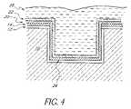
- FIG. 4is a schematic, cross-sectional side view of the substrate of FIG. 3 with a layer of spin-on dielectric material filling the trench.
- FIG. 5is a schematic, cross-sectional side view of the substrate of FIG. 4 after a curing and densification process.
- FIG. 6is a schematic, cross-sectional side view of the substrate of FIG. 5 after chemical mechanical polishing (CMP) the oxide down to the top nitride surface.
- CMPchemical mechanical polishing
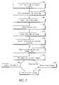
- FIG. 7is a flow chart of a process for shallow trench isolation in accordance with the preferred embodiment.
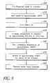
- FIG. 8is a flow chart of a process for densification of spin-on dielectric in accordance with the preferred embodiment of the present invention.
- SODspin-on dielectric
- a liner materialthat expands irreversibly when oxidized.
- a nitride layeris deposited to protect the active area of the trench.
- An expandable lineris deposited over the nitride liner before the trench is filled with a dielectric material. When the dielectric material is densified, the liner expands. The dielectric material reduces in size significantly as the material is densified. The expanding liner serves to evenly compress the dielectric material. In this manner, the combination of the liner and the densification process yields excellent bulk density in sub-micron spaces.
- the liner materialis preferably easily deposited in small spaces and irreversibly expanded when oxidized.
- the lineris amorphous silicon. As amorphous silicon oxidizes into silicon oxide, it expands. Other materials that expand upon oxidation, such as polysilicon, could also be used.
- the densification of the materials within sub-micron spacesis also helpful to the proper filling of the space.
- the waferis cured in a steam chamber. While the wafer is in the chamber, the temperature is increased. After the temperature reaches the target, the wafer anneal continues at a temperature plateau.
- the densification processhas the benefit of densifying the spin-on material sufficiently without damaging any of the surrounding materials. A beneficial result of this densification process is the matching of wet etch resistance in small and large features.
- An introductory stepis the creation of a sub-micron space, such as a trench for shallow trench isolation (STI).
- a semiconductor substrate 10e.g., a silicon wafer
- a thin “pad” oxide 12is thermally grown on the substrate.
- a thick layer of a silicon nitride 14preferably Si 3 N 4
- the nitride 14is preferably formed by chemical vapor deposition (CVD).
- This nitride layer 14acts as a stop for the chemical mechanical polishing (CMP) process.
- Exemplary thickness rangesare between about 30 ⁇ and 100 ⁇ for the pad oxide 12 and between about 200 ⁇ and 1500 ⁇ for the nitride layer 14 .
- a photoresist mask 16is applied to the substrate 10 in order to etch the trench.
- Photoresistis applied on the surface of the wafer.
- a reticle that blocks ultraviolet (UV) radiationis then placed over the wafer.
- the photoresistis then selectively exposed to UV radiation.
- the developing solutionwashes away either exposed or unexposed regions.
- the photoresist mask 16 of FIG. 2is removed by conventional resist strip process.
- a trenchcan be etched in two primary ways, isotropically or anisotropically.
- the anisotropic methodis directional and produces relatively straight, vertical sidewalls.
- One type of anisotropic etchis known as reactive ion etch (RIE).
- RIEreactive ion etch
- FIG. 2this method is quite accurate and straight; however, it damages sidewalls 18 of the trench, which define edges of transistor active areas.
- the sidewalls 18are preferably oxidized, forming a thin oxide layer 24 , in order to repair the damage from the prior RIE.
- an insulating oxygen barrierin the illustrated embodiment comprising another nitride layer 20 , is deposited in the trench, preferably by CVD.
- This layercan range in thickness of preferably between about 10 angstroms ( ⁇ ) and 300 ⁇ , more preferably between about 20 ⁇ and 200 ⁇ , and most preferably between about 30 ⁇ and 150 ⁇ .
- the nitride layer 20both protects the active area and acts as an oxygen barrier between the semiconductor layer and the filler materials.
- a thin expandable liner layer 22is formed in the trench.
- This liner layer 22can be formed in several ways, but the layer is preferably deposited using CVD.
- the liner materialpreferably expands during a densification process described below.
- the linerpreferably comprises amorphous silicon with a thickness of between about 20 ⁇ and 200 ⁇ , more preferably between 25 ⁇ and 150 ⁇ , most preferably between 50 ⁇ and 100 ⁇ .
- the lineris completely oxidized during the densification process described below. Because amorphous silicon is easy to apply using CVD and expands relatively uniformly upon oxidation, it makes an excellent liner layer 22 . Additionally, amorphous silicon makes a high quality oxide when oxidized.
- a spin-on deposition processis preferably used to deposit a dielectric material 26 into the remaining space in the trench, as shown in FIG. 4 .
- the thickness of this layer 26will vary based upon the size of the trench, but in the illustrated embodiment the thickness of the material is preferably between 2500 ⁇ and 5500 ⁇ , more preferably between 3000 ⁇ and 4500 ⁇ .
- Spin-on depositionuses liquid materials placed on a wafer. The wafer is then rapidly spun, which spreads the liquid uniformly over the surface of the wafer after filling the low points on the wafer.
- An example of a spin-on materialis SpinfilTM made by Clariant (Japan) K.K.—Life Science & Electronic Chemicals of Tokyo, Japan. However, the skilled practitioner will appreciate that many dielectric materials can be used for these purposes.
- TEOS CVDTEOS
- amorphous silicon linercould also be beneficial for this process.
- the amorphous silicon linerwould expand upon oxidation, compressing the TEOS filler. Skilled practitioners will appreciate that several deposition processes could be used to fill the trench.
- Clariantthe manufacturer of the spin-on dielectric (SOD) material, was found unsatisfactory for the purposes of such small spaces.
- Clariant's SpinfilTM SOD materialbased upon perhydrosilazane (SiH 2 NH), has a recommended baking recipe as follows:
- the densification processmust also be balanced by the need for the densification process to be mild enough to avoid oxidizing the nitride layer in addition to the SOD material and the amorphous silicon layer. If the nitride layer is oxidized, the semiconductor sidewalls that define the edges of transistor active areas could also be subsequently oxidized, thereby consuming critical transistor real estate. Also, preferably, the materials within the trench should not significantly shrink away from the walls much.
- a preferred embodiment of a densification processis shown in flow chart form in FIG. 8 .
- 200 a prepared waferis placed in a chamber.
- the waferis preferably heated 210 to an initial temperature of between about 200° C. and 600° C., more preferably between 300° C. and 500° C., most preferably between 350° C. and 450° C. in the chamber.
- steamis then turned on 220 in the chamber.
- the heatramps 230 up to a target temperature between approximately 800° C. and 1200° C., more preferably between 900° C. and 1100° C., and most preferably between 950° C. and 1050° C.
- the increase of the temperature in the chamberis stopped 240 when it gets to this target temperature.
- the temperaturecan increase approximately between about 3° C. per minute to 25° C. per minute, more preferably between about 8° C. and 20° C.
- the waferis in an oxidizing environment, preferably an ambient steam environment.
- the waferis annealed 250 for approximately 10 to 40 minutes, more preferably between 15 min and 35 min, at the temperature plateau on steady state.
- the waferis annealed in a second oxidizing environment, preferably in a dry oxygen (O 2 ) environment.
- O 2dry oxygen
- FIG. 5shows the trench and surrounding area after the densification process.
- a linear volume decreaseof preferably about 7% to 25%, or more preferably between about 12% and 18%, takes place.
- the volume of the spin-on dielectric materialwill shrink linearly by approximately 15% as it turns into a layer of silicon oxide 32 .
- the processwill oxidize both the SOD material and the amorphous silicon liner. As the SOD material oxidizes and shrinks, the preferred amorphous silicon layer will expand as it turns into a layer of liner silicon oxide 30 . If the thickness of the amorphous silicon layer is selected properly, the entirety of the layer will be consumed during the oxidation.
- the nitride liner 20 below the linerwill not be oxidized because the oxidation process is not that aggressive, and furthermore the liner 20 preferably getters excess oxidant. Both the SOD material and the liner will become forms of silicon oxide in the densification process. However, the filler silicon oxide 32 that was the SOD material may etch faster than the liner silicon oxide 30 that was the amorphous silicon liner.
- the expandable liner 22 of FIG. 4serves to compress the dielectric material evenly.
- the liner's functionsinclude compressing the dielectric materials evenly and acting as a getter of oxygen for the dielectric material during the densification process.
- a CMP or other etchback processcan be used to remove undesired materials on top of the wafer.
- the consistent and slow etch rates in the layers of silicon oxide 30 , 32substantially reduces any recess formed at the top of the trench.
- the nitride layer 20 in the trenchremains in the trench after the densification process to protect the active areas adjacent to the trench.
- the liner and the densification processyield two silicon oxide layers that have a neglible vertical wet etch rate gradient.
- the wet etch rateis substantially consistent from the top to the bottom of the trench in each of the layer.
- a narrower trenchwill have a bigger gradient.
- the even compression by the linercreates substantial uniformity of wet etch rate gradients in the densified dielectric material from trench to trench, even when one trench is significantly narrower.
- a trench with a width of wwill have a substantially similar wet etch rate gradient in the filler silicon oxide 32 as a trench with a width of 3 w, 5 w, or even 10 w.
- the vertical etch rate gradient of two trenches of widths varying by an order of magnitudeis within 5%, more preferably within 2%. This consistency is helpful when performing etches, CMPs, and wet cleans across an entire wafer.
- the filler materialdoes not have a seam as would result if the trench were filled using CVD process such as ozone TEOS. This avoids problems with subsequent processing, including planarizations and etches.
- FIG. 6shows the structure after the process is completed and the wafer has been through etching and a wet clean. It can be seen that there a substantially reduced recess on the top of the shallow trench.
- the nitride liner 20is not oxidized beneath the silicon oxide.
- the first, thinner liner oxide layer 30is a thermal oxide formed from the amorphous silicon liner.
- the second filler oxide layer 32is the thicker layer of silicon oxide, which is a spin-on dielectric. It typically has a higher wet etch rate than that of the thermal oxide in small features.
Landscapes
- Engineering & Computer Science (AREA)
- Physics & Mathematics (AREA)
- Condensed Matter Physics & Semiconductors (AREA)
- General Physics & Mathematics (AREA)
- Manufacturing & Machinery (AREA)
- Computer Hardware Design (AREA)
- Microelectronics & Electronic Packaging (AREA)
- Power Engineering (AREA)
- Element Separation (AREA)
Abstract
Description
SixNyHz+H2O→SiO2+H2+NH3
Claims (23)
Priority Applications (1)
| Application Number | Priority Date | Filing Date | Title |
|---|---|---|---|
| US11/557,014US7659181B2 (en) | 2004-02-19 | 2006-11-06 | Sub-micron space liner and filler process |
Applications Claiming Priority (3)
| Application Number | Priority Date | Filing Date | Title |
|---|---|---|---|
| US10/782,997US7112513B2 (en) | 2004-02-19 | 2004-02-19 | Sub-micron space liner and densification process |
| US11/497,665US7622769B2 (en) | 2004-02-19 | 2006-08-01 | Isolation trench |
| US11/557,014US7659181B2 (en) | 2004-02-19 | 2006-11-06 | Sub-micron space liner and filler process |
Related Parent Applications (1)
| Application Number | Title | Priority Date | Filing Date |
|---|---|---|---|
| US11/497,665ContinuationUS7622769B2 (en) | 2004-02-19 | 2006-08-01 | Isolation trench |
Publications (2)
| Publication Number | Publication Date |
|---|---|
| US20070059899A1 US20070059899A1 (en) | 2007-03-15 |
| US7659181B2true US7659181B2 (en) | 2010-02-09 |
Family
ID=34861117
Family Applications (3)
| Application Number | Title | Priority Date | Filing Date |
|---|---|---|---|
| US10/782,997Expired - LifetimeUS7112513B2 (en) | 2004-02-19 | 2004-02-19 | Sub-micron space liner and densification process |
| US11/497,665Expired - LifetimeUS7622769B2 (en) | 2004-02-19 | 2006-08-01 | Isolation trench |
| US11/557,014Expired - LifetimeUS7659181B2 (en) | 2004-02-19 | 2006-11-06 | Sub-micron space liner and filler process |
Family Applications Before (2)
| Application Number | Title | Priority Date | Filing Date |
|---|---|---|---|
| US10/782,997Expired - LifetimeUS7112513B2 (en) | 2004-02-19 | 2004-02-19 | Sub-micron space liner and densification process |
| US11/497,665Expired - LifetimeUS7622769B2 (en) | 2004-02-19 | 2006-08-01 | Isolation trench |
Country Status (1)
| Country | Link |
|---|---|
| US (3) | US7112513B2 (en) |
Cited By (1)
| Publication number | Priority date | Publication date | Assignee | Title |
|---|---|---|---|---|
| US20150014807A1 (en)* | 2013-07-10 | 2015-01-15 | Taiwan Semiconductor Manufacturing Company, Ltd. | Method of forming a shallow trench isolation structure |
Families Citing this family (49)
| Publication number | Priority date | Publication date | Assignee | Title |
|---|---|---|---|---|
| US7141483B2 (en) | 2002-09-19 | 2006-11-28 | Applied Materials, Inc. | Nitrous oxide anneal of TEOS/ozone CVD for improved gapfill |
| US7456116B2 (en)* | 2002-09-19 | 2008-11-25 | Applied Materials, Inc. | Gap-fill depositions in the formation of silicon containing dielectric materials |
| US7431967B2 (en)* | 2002-09-19 | 2008-10-07 | Applied Materials, Inc. | Limited thermal budget formation of PMD layers |
| US7101785B2 (en)* | 2003-07-22 | 2006-09-05 | Infineon Technologies Ag | Formation of a contact in a device, and the device including the contact |
| US20070212847A1 (en)* | 2004-08-04 | 2007-09-13 | Applied Materials, Inc. | Multi-step anneal of thin films for film densification and improved gap-fill |
| US7642171B2 (en) | 2004-08-04 | 2010-01-05 | Applied Materials, Inc. | Multi-step anneal of thin films for film densification and improved gap-fill |
| TWI238489B (en)* | 2004-12-09 | 2005-08-21 | Promos Technologies Inc | A method for forming a shallow trench isolation structure with reduced stress |
| US7273796B2 (en)* | 2005-03-23 | 2007-09-25 | Micron Technology, Inc. | Methods of forming trench isolation in the fabrication of integrated circuitry and methods of fabricating integrated circuitry |
| DE102005039667A1 (en)* | 2005-08-22 | 2007-03-01 | Infineon Technologies Ag | Producing a low aspect ratio structure and buried strap for a trench DRAM forms and fills trench in semiconductor substrate with initial and sacrificial layers and selectively removes especially at sidewalls |
| US7375004B2 (en)* | 2006-03-10 | 2008-05-20 | Micron Technology, Inc. | Method of making an isolation trench and resulting isolation trench |
| US20070224772A1 (en)* | 2006-03-21 | 2007-09-27 | Freescale Semiconductor, Inc. | Method for forming a stressor structure |
| CN101079391B (en)* | 2006-05-26 | 2012-01-25 | 中芯国际集成电路制造(上海)有限公司 | Method for semiconductor part with high clearance filling capability |
| US20070298583A1 (en)* | 2006-06-27 | 2007-12-27 | Macronix International Co., Ltd. | Method for forming a shallow trench isolation region |
| US7968425B2 (en) | 2006-07-14 | 2011-06-28 | Micron Technology, Inc. | Isolation regions |
| US7919800B2 (en) | 2007-02-26 | 2011-04-05 | Micron Technology, Inc. | Capacitor-less memory cells and cell arrays |
| US20080227267A1 (en)* | 2007-03-14 | 2008-09-18 | Theodorus Gerardus Maria Oosterlaken | Stop mechanism for trench reshaping process |
| KR100972675B1 (en)* | 2008-01-10 | 2010-07-27 | 주식회사 하이닉스반도체 | Device Separator Formation Method of Semiconductor Device |
| KR100945927B1 (en)* | 2008-03-05 | 2010-03-05 | 주식회사 하이닉스반도체 | Manufacturing Method of Semiconductor Memory Device |
| KR101436564B1 (en)* | 2008-05-07 | 2014-09-02 | 한국에이에스엠지니텍 주식회사 | Forming method of amorphous silicone thin film |
| US7655532B1 (en)* | 2008-07-25 | 2010-02-02 | Taiwan Semiconductor Manufacturing Company, Ltd. | STI film property using SOD post-treatment |
| US8963241B1 (en) | 2009-11-13 | 2015-02-24 | Maxim Integrated Products, Inc. | Integrated MOS power transistor with poly field plate extension for depletion assist |
| US8987818B1 (en) | 2009-11-13 | 2015-03-24 | Maxim Integrated Products, Inc. | Integrated MOS power transistor with thin gate oxide and low gate charge |
| US8946851B1 (en) | 2009-11-13 | 2015-02-03 | Maxim Integrated Products, Inc. | Integrated MOS power transistor with thin gate oxide and low gate charge |
| US20110115019A1 (en)* | 2009-11-13 | 2011-05-19 | Maxim Integrated Products, Inc. | Cmos compatible low gate charge lateral mosfet |
| US8969958B1 (en) | 2009-11-13 | 2015-03-03 | Maxim Integrated Products, Inc. | Integrated MOS power transistor with body extension region for poly field plate depletion assist |
| US20110115018A1 (en)* | 2009-11-13 | 2011-05-19 | Maxim Integrated Products, Inc. | Mos power transistor |
| US8048755B2 (en) | 2010-02-08 | 2011-11-01 | Micron Technology, Inc. | Resistive memory and methods of processing resistive memory |
| US8349653B2 (en) | 2010-06-02 | 2013-01-08 | Maxim Integrated Products, Inc. | Use of device assembly for a generalization of three-dimensional metal interconnect technologies |
| US10672748B1 (en) | 2010-06-02 | 2020-06-02 | Maxim Integrated Products, Inc. | Use of device assembly for a generalization of three-dimensional heterogeneous technologies integration |
| JP5490753B2 (en)* | 2010-07-29 | 2014-05-14 | 東京エレクトロン株式会社 | Trench filling method and film forming system |
| US7947551B1 (en)* | 2010-09-28 | 2011-05-24 | Taiwan Semiconductor Manufacturing Company, Ltd. | Method of forming a shallow trench isolation structure |
| JP5675331B2 (en)* | 2010-12-27 | 2015-02-25 | 東京エレクトロン株式会社 | How to fill trench |
| JP5977002B2 (en)* | 2011-08-25 | 2016-08-24 | 東京エレクトロン株式会社 | Trench filling method and semiconductor integrated circuit device manufacturing method |
| KR102002782B1 (en) | 2012-09-10 | 2019-07-23 | 삼성전자주식회사 | Method of manufacturing for Semiconductor device using expandable material |
| US9117878B2 (en)* | 2012-12-11 | 2015-08-25 | United Microelectronics Corp. | Method for manufacturing shallow trench isolation |
| US9018108B2 (en) | 2013-01-25 | 2015-04-28 | Applied Materials, Inc. | Low shrinkage dielectric films |
| US20150064929A1 (en)* | 2013-09-05 | 2015-03-05 | United Microelectronics Corp. | Method of gap filling |
| US9209040B2 (en)* | 2013-10-11 | 2015-12-08 | Taiwan Semiconductor Manufacturing Co., Ltd. | Amorphorus silicon insertion for STI-CMP planarity improvement |
| US9406544B1 (en)* | 2015-06-12 | 2016-08-02 | Lam Research Corporation | Systems and methods for eliminating seams in atomic layer deposition of silicon dioxide film in gap fill applications |
| KR102404642B1 (en)* | 2015-07-17 | 2022-06-03 | 삼성전자주식회사 | Semiconductor Device and Method of fabricating the same |
| US9871100B2 (en)* | 2015-07-29 | 2018-01-16 | Taiwan Semiconductor Manufacturing Co., Ltd. | Trench structure of semiconductor device having uneven nitrogen distribution liner |
| US9786496B2 (en) | 2015-08-17 | 2017-10-10 | Lam Research Corporation | Method of densifying films in semiconductor device |
| US9935000B2 (en) | 2016-02-29 | 2018-04-03 | Intel Corporation | Slit stress modulation in semiconductor substrates |
| CN110246842A (en)* | 2018-03-08 | 2019-09-17 | 联华电子股份有限公司 | A method of making semiconductor element |
| CN110707045B (en)* | 2018-10-09 | 2023-05-12 | 联华电子股份有限公司 | Method for manufacturing semiconductor element |
| US20200203216A1 (en)* | 2018-12-24 | 2020-06-25 | Xia Tai Xin Semiconductor (Qing Dao) Ltd. | Method of forming semiconductor structure |
| CN114334791B (en)* | 2020-09-30 | 2024-10-25 | 长鑫存储技术有限公司 | Method for forming semiconductor structure and semiconductor structure |
| CN115863413A (en)* | 2023-03-01 | 2023-03-28 | 通威微电子有限公司 | Method for manufacturing trench oxide layer and semiconductor device |
| US20250046708A1 (en)* | 2023-08-04 | 2025-02-06 | Nanya Technology Corporation | Semiconductor device with protection layer and method for fabricating the same |
Citations (30)
| Publication number | Priority date | Publication date | Assignee | Title |
|---|---|---|---|---|
| US4855804A (en) | 1987-11-17 | 1989-08-08 | Motorola, Inc. | Multilayer trench isolation process and structure |
| US5087586A (en) | 1991-07-03 | 1992-02-11 | Micron Technology, Inc. | Process for creating fully-recessed field isolation regions by oxidizing a selectively-grown epitaxial silicon layer |
| US5190889A (en) | 1991-12-09 | 1993-03-02 | Motorola, Inc. | Method of forming trench isolation structure with germanium silicate filling |
| US5387540A (en) | 1993-09-30 | 1995-02-07 | Motorola Inc. | Method of forming trench isolation structure in an integrated circuit |
| US5447884A (en) | 1994-06-29 | 1995-09-05 | International Business Machines Corporation | Shallow trench isolation with thin nitride liner |
| US5492858A (en) | 1994-04-20 | 1996-02-20 | Digital Equipment Corporation | Shallow trench isolation process for high aspect ratio trenches |
| US5702976A (en) | 1995-10-24 | 1997-12-30 | Micron Technology, Inc. | Shallow trench isolation using low dielectric constant insulator |
| US5869384A (en) | 1997-03-17 | 1999-02-09 | Taiwan Semiconductor Manufacturing Company, Ltd. | Trench filling method employing silicon liner layer and gap filling silicon oxide trench fill layer |
| US5926717A (en) | 1996-12-10 | 1999-07-20 | Advanced Micro Devices, Inc. | Method of making an integrated circuit with oxidizable trench liner |
| US5943585A (en) | 1997-12-19 | 1999-08-24 | Advanced Micro Devices, Inc. | Trench isolation structure having low K dielectric spacers arranged upon an oxide liner incorporated with nitrogen |
| US6027982A (en) | 1999-02-05 | 2000-02-22 | Chartered Semiconductor Manufacturing Ltd. | Method to form shallow trench isolation structures with improved isolation fill and surface planarity |
| US6037238A (en) | 1999-01-04 | 2000-03-14 | Vanguard International Semiconductor Corporation | Process to reduce defect formation occurring during shallow trench isolation formation |
| US6046487A (en) | 1997-01-28 | 2000-04-04 | International Business Machines Corporation | Shallow trench isolation with oxide-nitride/oxynitride liner |
| US6180490B1 (en) | 1999-05-25 | 2001-01-30 | Chartered Semiconductor Manufacturing Ltd. | Method of filling shallow trenches |
| US6187651B1 (en) | 1998-05-07 | 2001-02-13 | Samsung Electronics Co., Ltd. | Methods of forming trench isolation regions using preferred stress relieving layers and techniques to inhibit the occurrence of voids |
| US6316331B1 (en) | 2000-10-13 | 2001-11-13 | Vanguard International Semiconductor Corp. | Method of making dishing-free insulator in trench isolation |
| US20020022326A1 (en) | 1999-11-11 | 2002-02-21 | Mitsubishi Denki Kabushiki Kaisha | Semiconductor device and method of manufacturing the same |
| US20020064937A1 (en) | 2000-11-30 | 2002-05-30 | Jae-Hak Kim | Methods of manufacturing integrated circuit devices in which a spin on glass insulation layer is dissolved so as to recess the spin on glass insulation layer from the upper surface of a pattern |
| US6461937B1 (en) | 1999-01-11 | 2002-10-08 | Samsung Electronics Co., Ltd. | Methods of forming trench isolation regions having recess-inhibiting layers therein that protect against overetching |
| US6500726B2 (en) | 2000-08-01 | 2002-12-31 | Samsung Electronics Co., Ltd. | Shallow trench isolation type semiconductor device and method of forming the same |
| US20030022522A1 (en) | 2001-07-13 | 2003-01-30 | Yukio Nishiyama | Method for manufacturing semiconductor device |
| US6518148B1 (en) | 2001-09-06 | 2003-02-11 | Taiwan Semiconductor Manufacturing Company, Ltd | Method for protecting STI structures with low etching rate liners |
| US6576558B1 (en) | 2002-10-02 | 2003-06-10 | Taiwan Semiconductor Manufacturing Company | High aspect ratio shallow trench using silicon implanted oxide |
| US6657276B1 (en) | 2001-12-10 | 2003-12-02 | Advanced Micro Devices, Inc. | Shallow trench isolation (STI) region with high-K liner and method of formation |
| US6699799B2 (en) | 2001-05-09 | 2004-03-02 | Samsung Electronics Co., Ltd. | Method of forming a semiconductor device |
| US20040099928A1 (en) | 2002-11-27 | 2004-05-27 | Nunan Thomas K. | Composite dielectric with improved etch selectivity for high voltage mems structures |
| US20050026443A1 (en)* | 2003-08-01 | 2005-02-03 | Goo Ju-Seon | Method for forming a silicon oxide layer using spin-on glass |
| US6956276B2 (en) | 2000-12-27 | 2005-10-18 | Kabushiki Kaisha Toshiba | Semiconductor device with an L-shaped/reversed L-shaped gate side-wall insulating film |
| US7176104B1 (en) | 2004-06-08 | 2007-02-13 | Integrated Device Technology, Inc. | Method for forming shallow trench isolation structure with deep oxide region |
| US7271463B2 (en) | 2004-12-10 | 2007-09-18 | Micron Technology, Inc. | Trench insulation structures including an oxide liner that is thinner along the walls of the trench than along the base |
Family Cites Families (2)
| Publication number | Priority date | Publication date | Assignee | Title |
|---|---|---|---|---|
| US5067588A (en)* | 1990-04-09 | 1991-11-26 | R. D. Werner Co., Inc. | Ladder lash |
| US6037937A (en)* | 1997-12-04 | 2000-03-14 | Nortel Networks Corporation | Navigation tool for graphical user interface |
- 2004
- 2004-02-19USUS10/782,997patent/US7112513B2/ennot_activeExpired - Lifetime
- 2006
- 2006-08-01USUS11/497,665patent/US7622769B2/ennot_activeExpired - Lifetime
- 2006-11-06USUS11/557,014patent/US7659181B2/ennot_activeExpired - Lifetime
Patent Citations (31)
| Publication number | Priority date | Publication date | Assignee | Title |
|---|---|---|---|---|
| US4855804A (en) | 1987-11-17 | 1989-08-08 | Motorola, Inc. | Multilayer trench isolation process and structure |
| US5087586A (en) | 1991-07-03 | 1992-02-11 | Micron Technology, Inc. | Process for creating fully-recessed field isolation regions by oxidizing a selectively-grown epitaxial silicon layer |
| US5190889A (en) | 1991-12-09 | 1993-03-02 | Motorola, Inc. | Method of forming trench isolation structure with germanium silicate filling |
| US5387540A (en) | 1993-09-30 | 1995-02-07 | Motorola Inc. | Method of forming trench isolation structure in an integrated circuit |
| US5492858A (en) | 1994-04-20 | 1996-02-20 | Digital Equipment Corporation | Shallow trench isolation process for high aspect ratio trenches |
| US5447884A (en) | 1994-06-29 | 1995-09-05 | International Business Machines Corporation | Shallow trench isolation with thin nitride liner |
| US5702976A (en) | 1995-10-24 | 1997-12-30 | Micron Technology, Inc. | Shallow trench isolation using low dielectric constant insulator |
| US5926717A (en) | 1996-12-10 | 1999-07-20 | Advanced Micro Devices, Inc. | Method of making an integrated circuit with oxidizable trench liner |
| US6046487A (en) | 1997-01-28 | 2000-04-04 | International Business Machines Corporation | Shallow trench isolation with oxide-nitride/oxynitride liner |
| US5869384A (en) | 1997-03-17 | 1999-02-09 | Taiwan Semiconductor Manufacturing Company, Ltd. | Trench filling method employing silicon liner layer and gap filling silicon oxide trench fill layer |
| US5943585A (en) | 1997-12-19 | 1999-08-24 | Advanced Micro Devices, Inc. | Trench isolation structure having low K dielectric spacers arranged upon an oxide liner incorporated with nitrogen |
| US6187651B1 (en) | 1998-05-07 | 2001-02-13 | Samsung Electronics Co., Ltd. | Methods of forming trench isolation regions using preferred stress relieving layers and techniques to inhibit the occurrence of voids |
| US6037238A (en) | 1999-01-04 | 2000-03-14 | Vanguard International Semiconductor Corporation | Process to reduce defect formation occurring during shallow trench isolation formation |
| US6461937B1 (en) | 1999-01-11 | 2002-10-08 | Samsung Electronics Co., Ltd. | Methods of forming trench isolation regions having recess-inhibiting layers therein that protect against overetching |
| US6717231B2 (en) | 1999-01-11 | 2004-04-06 | Samsung Electronics Co., Ltd. | Trench isolation regions having recess-inhibiting layers therein that protect against overetching |
| US6027982A (en) | 1999-02-05 | 2000-02-22 | Chartered Semiconductor Manufacturing Ltd. | Method to form shallow trench isolation structures with improved isolation fill and surface planarity |
| US6180490B1 (en) | 1999-05-25 | 2001-01-30 | Chartered Semiconductor Manufacturing Ltd. | Method of filling shallow trenches |
| US20020022326A1 (en) | 1999-11-11 | 2002-02-21 | Mitsubishi Denki Kabushiki Kaisha | Semiconductor device and method of manufacturing the same |
| US6500726B2 (en) | 2000-08-01 | 2002-12-31 | Samsung Electronics Co., Ltd. | Shallow trench isolation type semiconductor device and method of forming the same |
| US6316331B1 (en) | 2000-10-13 | 2001-11-13 | Vanguard International Semiconductor Corp. | Method of making dishing-free insulator in trench isolation |
| US20020064937A1 (en) | 2000-11-30 | 2002-05-30 | Jae-Hak Kim | Methods of manufacturing integrated circuit devices in which a spin on glass insulation layer is dissolved so as to recess the spin on glass insulation layer from the upper surface of a pattern |
| US6956276B2 (en) | 2000-12-27 | 2005-10-18 | Kabushiki Kaisha Toshiba | Semiconductor device with an L-shaped/reversed L-shaped gate side-wall insulating film |
| US6699799B2 (en) | 2001-05-09 | 2004-03-02 | Samsung Electronics Co., Ltd. | Method of forming a semiconductor device |
| US20030022522A1 (en) | 2001-07-13 | 2003-01-30 | Yukio Nishiyama | Method for manufacturing semiconductor device |
| US6518148B1 (en) | 2001-09-06 | 2003-02-11 | Taiwan Semiconductor Manufacturing Company, Ltd | Method for protecting STI structures with low etching rate liners |
| US6657276B1 (en) | 2001-12-10 | 2003-12-02 | Advanced Micro Devices, Inc. | Shallow trench isolation (STI) region with high-K liner and method of formation |
| US6576558B1 (en) | 2002-10-02 | 2003-06-10 | Taiwan Semiconductor Manufacturing Company | High aspect ratio shallow trench using silicon implanted oxide |
| US20040099928A1 (en) | 2002-11-27 | 2004-05-27 | Nunan Thomas K. | Composite dielectric with improved etch selectivity for high voltage mems structures |
| US20050026443A1 (en)* | 2003-08-01 | 2005-02-03 | Goo Ju-Seon | Method for forming a silicon oxide layer using spin-on glass |
| US7176104B1 (en) | 2004-06-08 | 2007-02-13 | Integrated Device Technology, Inc. | Method for forming shallow trench isolation structure with deep oxide region |
| US7271463B2 (en) | 2004-12-10 | 2007-09-18 | Micron Technology, Inc. | Trench insulation structures including an oxide liner that is thinner along the walls of the trench than along the base |
Non-Patent Citations (3)
| Title |
|---|
| Advertisement entitled "Polysilazane SODs Spinfir(TM) 400 Series for STI/PMD Application," May 2004. |
| Advertisement entitled "Polysilazane SODs Spinfir™ 400 Series for STI/PMD Application," May 2004. |
| Peters, Laura, "Choices and challenges for shallow trench isolation," Semiconductor International, Website www.ree-electronics.com, Apr. 1, 1999, 6 pages. |
Cited By (4)
| Publication number | Priority date | Publication date | Assignee | Title |
|---|---|---|---|---|
| US20150014807A1 (en)* | 2013-07-10 | 2015-01-15 | Taiwan Semiconductor Manufacturing Company, Ltd. | Method of forming a shallow trench isolation structure |
| US8975155B2 (en)* | 2013-07-10 | 2015-03-10 | Taiwan Semiconductor Manufacturing Company, Ltd. | Method of forming a shallow trench isolation structure |
| US9209243B2 (en) | 2013-07-10 | 2015-12-08 | Taiwan Semiconductor Manufacturing Company, Ltd. | Method of forming a shallow trench isolation structure |
| KR101615814B1 (en) | 2013-07-10 | 2016-04-26 | 타이완 세미콘덕터 매뉴팩쳐링 컴퍼니 리미티드 | Method of forming a shallow trench isolation structure |
Also Published As
| Publication number | Publication date |
|---|---|
| US20050186755A1 (en) | 2005-08-25 |
| US20060267131A1 (en) | 2006-11-30 |
| US7622769B2 (en) | 2009-11-24 |
| US7112513B2 (en) | 2006-09-26 |
| US20070059899A1 (en) | 2007-03-15 |
Similar Documents
| Publication | Publication Date | Title |
|---|---|---|
| US7659181B2 (en) | Sub-micron space liner and filler process | |
| US7919829B2 (en) | Liner for shallow trench isolation | |
| US7416987B2 (en) | Semiconductor device and method of fabricating the same | |
| US7501691B2 (en) | Trench insulation structures including an oxide liner and oxidation barrier | |
| US6048775A (en) | Method to make shallow trench isolation structure by HDP-CVD and chemical mechanical polish processes | |
| US7682927B2 (en) | Method of manufacturing semiconductor device | |
| KR20090067576A (en) | Trench embedding method and formation method of device isolation structure using same | |
| US6787409B2 (en) | Method of forming trench isolation without grooving | |
| US6331472B1 (en) | Method for forming shallow trench isolation | |
| KR100567022B1 (en) | Device isolation film formation method using trench of semiconductor device | |
| US20050255668A1 (en) | Method of fabricating shallow trench isolation structure | |
| US6602759B2 (en) | Shallow trench isolation for thin silicon/silicon-on-insulator substrates by utilizing polysilicon | |
| US6214695B1 (en) | Method of manufacturing semiconductor device | |
| US6060394A (en) | Method for forming shallow trench isolation with global planarization | |
| US6103581A (en) | Method for producing shallow trench isolation structure | |
| KR100677998B1 (en) | Shallow Trench Isolation Method for Semiconductor Devices | |
| US6869857B2 (en) | Method to achieve STI planarization | |
| KR100381849B1 (en) | Trench isolation method | |
| US20020137305A1 (en) | Fabrication method of shallow trench isolation | |
| US7314809B2 (en) | Method for forming a shallow trench isolation structure with reduced stress | |
| US20010053583A1 (en) | Shallow trench isolation formation process using a sacrificial layer | |
| KR100508865B1 (en) | Method for fabricating trench of semiconductor device | |
| KR20020051351A (en) | Method for isolating semiconductor devices |
Legal Events
| Date | Code | Title | Description |
|---|---|---|---|
| FEPP | Fee payment procedure | Free format text:PAYOR NUMBER ASSIGNED (ORIGINAL EVENT CODE: ASPN); ENTITY STATUS OF PATENT OWNER: LARGE ENTITY | |
| STCF | Information on status: patent grant | Free format text:PATENTED CASE | |
| CC | Certificate of correction | ||
| FPAY | Fee payment | Year of fee payment:4 | |
| AS | Assignment | Owner name:U.S. BANK NATIONAL ASSOCIATION, AS COLLATERAL AGENT, CALIFORNIA Free format text:SECURITY INTEREST;ASSIGNOR:MICRON TECHNOLOGY, INC.;REEL/FRAME:038669/0001 Effective date:20160426 Owner name:U.S. BANK NATIONAL ASSOCIATION, AS COLLATERAL AGEN Free format text:SECURITY INTEREST;ASSIGNOR:MICRON TECHNOLOGY, INC.;REEL/FRAME:038669/0001 Effective date:20160426 | |
| AS | Assignment | Owner name:MORGAN STANLEY SENIOR FUNDING, INC., AS COLLATERAL AGENT, MARYLAND Free format text:PATENT SECURITY AGREEMENT;ASSIGNOR:MICRON TECHNOLOGY, INC.;REEL/FRAME:038954/0001 Effective date:20160426 Owner name:MORGAN STANLEY SENIOR FUNDING, INC., AS COLLATERAL Free format text:PATENT SECURITY AGREEMENT;ASSIGNOR:MICRON TECHNOLOGY, INC.;REEL/FRAME:038954/0001 Effective date:20160426 | |
| AS | Assignment | Owner name:U.S. BANK NATIONAL ASSOCIATION, AS COLLATERAL AGENT, CALIFORNIA Free format text:CORRECTIVE ASSIGNMENT TO CORRECT THE REPLACE ERRONEOUSLY FILED PATENT #7358718 WITH THE CORRECT PATENT #7358178 PREVIOUSLY RECORDED ON REEL 038669 FRAME 0001. ASSIGNOR(S) HEREBY CONFIRMS THE SECURITY INTEREST;ASSIGNOR:MICRON TECHNOLOGY, INC.;REEL/FRAME:043079/0001 Effective date:20160426 Owner name:U.S. BANK NATIONAL ASSOCIATION, AS COLLATERAL AGEN Free format text:CORRECTIVE ASSIGNMENT TO CORRECT THE REPLACE ERRONEOUSLY FILED PATENT #7358718 WITH THE CORRECT PATENT #7358178 PREVIOUSLY RECORDED ON REEL 038669 FRAME 0001. ASSIGNOR(S) HEREBY CONFIRMS THE SECURITY INTEREST;ASSIGNOR:MICRON TECHNOLOGY, INC.;REEL/FRAME:043079/0001 Effective date:20160426 | |
| FPAY | Fee payment | Year of fee payment:8 | |
| AS | Assignment | Owner name:JPMORGAN CHASE BANK, N.A., AS COLLATERAL AGENT, ILLINOIS Free format text:SECURITY INTEREST;ASSIGNORS:MICRON TECHNOLOGY, INC.;MICRON SEMICONDUCTOR PRODUCTS, INC.;REEL/FRAME:047540/0001 Effective date:20180703 Owner name:JPMORGAN CHASE BANK, N.A., AS COLLATERAL AGENT, IL Free format text:SECURITY INTEREST;ASSIGNORS:MICRON TECHNOLOGY, INC.;MICRON SEMICONDUCTOR PRODUCTS, INC.;REEL/FRAME:047540/0001 Effective date:20180703 | |
| AS | Assignment | Owner name:MICRON TECHNOLOGY, INC., IDAHO Free format text:RELEASE BY SECURED PARTY;ASSIGNOR:U.S. BANK NATIONAL ASSOCIATION, AS COLLATERAL AGENT;REEL/FRAME:047243/0001 Effective date:20180629 | |
| AS | Assignment | Owner name:MICRON TECHNOLOGY, INC., IDAHO Free format text:RELEASE BY SECURED PARTY;ASSIGNOR:MORGAN STANLEY SENIOR FUNDING, INC., AS COLLATERAL AGENT;REEL/FRAME:050937/0001 Effective date:20190731 | |
| AS | Assignment | Owner name:MICRON SEMICONDUCTOR PRODUCTS, INC., IDAHO Free format text:RELEASE BY SECURED PARTY;ASSIGNOR:JPMORGAN CHASE BANK, N.A., AS COLLATERAL AGENT;REEL/FRAME:051028/0001 Effective date:20190731 Owner name:MICRON TECHNOLOGY, INC., IDAHO Free format text:RELEASE BY SECURED PARTY;ASSIGNOR:JPMORGAN CHASE BANK, N.A., AS COLLATERAL AGENT;REEL/FRAME:051028/0001 Effective date:20190731 | |
| MAFP | Maintenance fee payment | Free format text:PAYMENT OF MAINTENANCE FEE, 12TH YEAR, LARGE ENTITY (ORIGINAL EVENT CODE: M1553); ENTITY STATUS OF PATENT OWNER: LARGE ENTITY Year of fee payment:12 |