US7656358B2 - Antenna operable at two frequency bands simultaneously - Google Patents
Antenna operable at two frequency bands simultaneouslyDownload PDFInfo
- Publication number
- US7656358B2 US7656358B2US11/931,610US93161007AUS7656358B2US 7656358 B2US7656358 B2US 7656358B2US 93161007 AUS93161007 AUS 93161007AUS 7656358 B2US7656358 B2US 7656358B2
- Authority
- US
- United States
- Prior art keywords
- antenna
- radiating
- array
- elements
- radiation
- Prior art date
- Legal status (The legal status is an assumption and is not a legal conclusion. Google has not performed a legal analysis and makes no representation as to the accuracy of the status listed.)
- Expired - Fee Related, expires
Links
- 230000005855radiationEffects0.000claimsdescription86
- 230000008878couplingEffects0.000claimsdescription35
- 238000010168coupling processMethods0.000claimsdescription35
- 238000005859coupling reactionMethods0.000claimsdescription35
- 230000013011matingEffects0.000claimsdescription6
- 230000010287polarizationEffects0.000description52
- 238000000034methodMethods0.000description17
- 230000001902propagating effectEffects0.000description13
- 238000005516engineering processMethods0.000description12
- 238000003491arrayMethods0.000description10
- 238000004519manufacturing processMethods0.000description10
- 230000005540biological transmissionEffects0.000description9
- 238000005388cross polarizationMethods0.000description8
- 230000005284excitationEffects0.000description8
- 230000007246mechanismEffects0.000description8
- 230000009977dual effectEffects0.000description7
- 230000008901benefitEffects0.000description6
- 230000006870functionEffects0.000description6
- 230000008569processEffects0.000description5
- 230000000694effectsEffects0.000description4
- 230000001965increasing effectEffects0.000description4
- 239000002184metalSubstances0.000description4
- 230000003068static effectEffects0.000description4
- 230000005672electromagnetic fieldEffects0.000description3
- 230000033001locomotionEffects0.000description3
- 239000000463materialSubstances0.000description3
- 239000011159matrix materialSubstances0.000description3
- 230000010363phase shiftEffects0.000description3
- 239000004033plasticSubstances0.000description3
- 230000009467reductionEffects0.000description3
- 230000009286beneficial effectEffects0.000description2
- 230000015572biosynthetic processEffects0.000description2
- 230000001413cellular effectEffects0.000description2
- 238000004891communicationMethods0.000description2
- 230000005670electromagnetic radiationEffects0.000description2
- 239000012212insulatorSubstances0.000description2
- 239000000758substrateSubstances0.000description2
- 239000004809TeflonSubstances0.000description1
- 229920006362Teflon®Polymers0.000description1
- 230000006978adaptationEffects0.000description1
- 230000008859changeEffects0.000description1
- 239000004020conductorSubstances0.000description1
- 238000010276constructionMethods0.000description1
- 238000001125extrusionMethods0.000description1
- 238000001914filtrationMethods0.000description1
- 230000001939inductive effectEffects0.000description1
- 238000003780insertionMethods0.000description1
- 230000037431insertionEffects0.000description1
- 238000009434installationMethods0.000description1
- 230000010354integrationEffects0.000description1
- 230000001788irregularEffects0.000description1
- 230000005404monopoleEffects0.000description1
- 230000003094perturbing effectEffects0.000description1
- 230000004044responseEffects0.000description1
- 238000007493shaping processMethods0.000description1
- 230000008054signal transmissionEffects0.000description1
Images


Classifications
- H—ELECTRICITY
- H01—ELECTRIC ELEMENTS
- H01Q—ANTENNAS, i.e. RADIO AERIALS
- H01Q13/00—Waveguide horns or mouths; Slot antennas; Leaky-waveguide antennas; Equivalent structures causing radiation along the transmission path of a guided wave
- H—ELECTRICITY
- H01—ELECTRIC ELEMENTS
- H01Q—ANTENNAS, i.e. RADIO AERIALS
- H01Q13/00—Waveguide horns or mouths; Slot antennas; Leaky-waveguide antennas; Equivalent structures causing radiation along the transmission path of a guided wave
- H01Q13/02—Waveguide horns
- H01Q13/0233—Horns fed by a slotted waveguide array
- H—ELECTRICITY
- H01—ELECTRIC ELEMENTS
- H01Q—ANTENNAS, i.e. RADIO AERIALS
- H01Q21/00—Antenna arrays or systems
- H01Q21/06—Arrays of individually energised antenna units similarly polarised and spaced apart
- H01Q21/061—Two dimensional planar arrays
- H01Q21/064—Two dimensional planar arrays using horn or slot aerials
Definitions
- the general field of the inventionrelates to a unique antenna arrangement for radiating and receiving electromagnetic radiation at two frequency bands simultaneously.
- an antennaconsists of a radiating element made of conductors that generate radiating electromagnetic field in response to an applied electric and the associated magnetic field.
- the processis bi-directional, i.e., when placed in an electromagnetic field, the field will induce an alternating current in the antenna and a voltage would be generated between the antenna's terminals or structure.
- the feed network, or transmission networkconveys the signal between the antenna and the transceiver (source or receiver).
- the feeding networkmay include antenna coupling networks and/or waveguides.
- An antenna arrayrefers to two or more antennas coupled to a common source or load so as to produce a directional radiation pattern. The spatial relationship between individual antennas contributes to the directivity of the antenna.
- DBSDirect Broadcast Satellite
- Fixed DBSreception is accomplished with a directional antenna aimed at a geostationary satellite.
- the antennaIn mobile DBS, the antenna is situated on a moving vehicle (earth bound, marine, or airborne). In such a situation, as the vehicle moves, the antenna needs to be continuously aimed at the satellite.
- Various mechanismsare used to cause the antenna to track the satellite during motion, such as a motorized mechanism and/or use of phase-shift antenna arrays. Further general information about mobile DBS can be found in, e.g., U.S. Pat. No. 6,529,706, which is incorporated herein by reference.
- phased array designin which each element of the array has a phase shifter and amplifier connected thereto.
- a typical array design for planar arraysuses either micro-strip technology or slotted waveguide technology (see, e.g., U.S. Pat. No. 5,579,019).
- micro-strip technologyantenna efficiency greatly diminishes as the size of the antenna increases.
- slotted waveguide technologythe systems incorporate complex components and bends, and very narrow slots, the dimensions and geometry of all of which have to be tightly controlled during the manufacturing process.
- the phase shifters and amplifiersare used to provide two-dimensional, hemispherical coverage.
- phase shiftersare costly and, particularly if the phased array incorporates many elements, the overall antenna cost can be quite high.
- phase shiftersrequire separate, complex control circuitry, which translates into unreasonable cost and system complexity.
- GBSGlobal Broadcast Service
- GBSGlobal Broadcast Service
- the GBS systemdeveloped by the Space Technology Branch of Communication-Electronics Command's Space and Terrestrial Communications Directorate uses a slotted waveguide antenna with a mechanized tracking system. While that antenna is said to have a low profile—extending to a height of “only” 14 inches without the radome (radar dome)—its size may be acceptable for military applications, but not acceptable for consumer applications, e.g., for private automobiles. For consumer applications the antenna should be of such a low profile as not to degrade the aesthetic appearance of the vehicle and not to significantly increase its drag coefficient.
- phase shifters of known systemsinherently add loss to the respective systems (e.g., 3 dB losses or more), thus requiring a substantial increase in antenna size in order to compensate for the loss.
- the sizemight reach 4 feet by 4 feet, which is impractical for consumer applications.
- Embodiments of the present inventionprovide an antenna capable of simultaneously operating at two frequency bands.
- the antennaincludes a square waveguide cavity, at least one radiating element, a plurality of second radiating elements, and a radiation source.
- the square waveguide cavityhas a top surface, bottom surface, and four sidewalls.
- the at least one radiating elementis optimized for operation at a first frequency band and is provided on the top surface symmetrically about the waveguide cavity's diagonal.
- the plurality of second radiating elementsare each optimized for operation at a second band of frequencies, and are provided on the top surface symmetrically about the waveguide cavity's diagonal.
- the radiation sourceis coupling a planar wave into the waveguide cavity through one of the sidewalls.
- the antennaalso includes a second radiation source coupling a second planar wave into the waveguide cavity from another one of the sidewalls.
- the antennaalso includes a third radiation source coupling a third planar wave into the waveguide cavity from a third one of the sidewalls and a fourth radiation source coupling a fourth planar wave into the waveguide cavity from a fourth one of the sidewalls.
- the at least one radiating elementincludes an array of n ⁇ n elements, each of which is symmetrical with respect to two axes residing on the same plane and extending normally to each other from the center of each of the n ⁇ n elements.
- the plurality of second radiating elementsmay be arranged at an L-shape about the array of n ⁇ n elements.
- Each of the n ⁇ n elementsmay include a conductive cone having size optimized for coupling RF energy at the first frequency band.
- Each of the plurality of second radiating elementsmay include a conductive cone having size optimized for coupling RF energy at the second frequency band.
- the radiation sourceis optimized for operating with the n ⁇ n array and further includes a second radiation source optimized for operating with the plurality of second radiating elements.
- each of the n ⁇ n elementsare sized to couple energy at Ka frequency band, and each of the second radiating elements is sized to couple energy at Ku frequency band.
- the cavityincludes a first height at area under the n ⁇ n array and a second height, smaller than the first height, at area under that second radiating elements.
- the first heightmay be optimized for guising wave energy at the first frequency band while the second height is optimized for guiding wave energy at the second frequency band.
- the radiation sourcecouples energy through first and second sidewalls
- the second radiation sourcecouples energy through a third and fourth ones of the sidewalls.
- each of the radiation source and second radiation courseincludes a pair of mating conductive element and radiation reflector configured such that radiation energy emitted from the conductive element is reflected by the reflector to couple a planar wave into the cavity through one of the sidewalls.
- the conductive elementincludes one of: metallic pin, metallic pin with counter reflector, a movable radiating pin, multiple radiating pins, microstrip patch, and microstrip array.
- the antennaalso includes waveguide extensions, each coupled between one of the sidewalls and one of the pair of mating conductive element and radiation reflector.
- each of the radiation source and second radiation courseincludes a conductive element and a radiation reflector.
- the radiation reflectoris configured such that radiation energy emitted from the conductive element is reflected by the reflector to thereby couple a planar wave into the cavity.
- the antennaalso includes waveguide extensions that are each coupled between one of the sidewalls and one of the pair of mating conductive element and radiation reflector.
- FIGS. 1A and 1Bdepict an example of an antenna according to an embodiment of the invention.
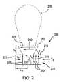
- FIG. 2illustrates a cross section of an antenna according to the embodiment of FIGS. 1A and 1B .
- FIG. 3Adepicts an embodiment of an antenna that may be used to transmit/receive two waves of cross polarization.
- FIG. 3Bdepicts a cross section similar to that of FIG. 2 , except that the arrangement enables excitation of two orthogonal polarizations from the same face.
- FIG. 4depicts an antenna according to another embodiment of the invention.
- FIG. 5depicts another embodiment of an antenna according to the subject invention.
- FIG. 6illustrates an embodiment optimized for operation at two different frequencies and optionally two different polarizations.
- FIG. 7depicts an embodiment of the invention using a radiating element having flared sidewalls.
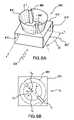
- FIG. 8Adepicts an embodiment of an antenna optimized for circularly polarized radiation.
- FIG. 8Bis a top view of the embodiment of FIG. 8A .
- FIG. 8Cdepicts another embodiment of an antenna optimized for circularly polarized radiation.
- FIG. 8Dillustrate a top view of a square circularly polarizing radiating element
- FIG. 8Eillustrates a top view of a cross-shaped circularly polarizing radiating element.
- FIG. 9illustrates a linear antenna array according to an embodiment of the invention.
- FIG. 10provides a cross-section of the embodiment of FIG. 9 .
- FIG. 11illustrates a linear array fed by a sectorial horn as a source, according to an embodiment of the invention.
- FIG. 12Aillustrates an example of a two-dimensional array according to an embodiment of the invention
- FIG. 12Billustrates a two-dimensional array according to another embodiment of the invention configured for operation with two sources.
- FIG. 12Cis a top view of the array illustrated in FIG. 12B .
- FIG. 13illustrates and example of a circular array antenna according to an embodiment of the invention.
- FIG. 14is a top view of another embodiment of a circular array antenna of the invention.
- FIG. 15illustrates a process of designing a Cartesian coordinate array according to an embodiment of the invention.
- FIGS. 16 and 16 A- 16 Eillustrate embodiments of an RF Source reflector feed for planer wave in near field regime of the electromagnetic field, according to the invention.
- FIG. 17illustrate another embodiment of an RF feed that includes several different collection pins, which corresponds to different beam locations (MultiBeam feed arrangement)
- FIG. 18illustrates an embodiment having dual-feed arrangement, for the benefit of generating dual polarization, multiple beam antenna.
- the Two orthogonal feedseach excites the array from a different face and thus generates dual orthogonal polarizations.
- FIG. 19illustrates the principle of beam tilt/scanning over the diagonal of a symmetrical array, with dual polarization capabilities.
- FIGS. 20A-20Cillustrate an embodiment wherein the inventive reflector feed is utilized for an array operating in two frequencies of different bands.
- Thisis the mixed array concept which employs two set of elements, one for each band, where the high band elements are in frequency cutoff for the lower frequency band, and situated in two square array formation. The smaller square array formation on the upper right hand corner is being fed at the lower frequency and its elements can support the higher band as well.
- FIGS. 20D and 20Eillustrate variations for the reflector feeds for the mixed array concept.
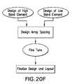
- FIG. 20Fillustrates a flow chart for the design of a mixed array antenna.
- FIGS. 21A and 21Billustrate another embodiment of the invention enabling simultaneous dual polarization with wide-angle reception, and easily installable antenna.
- FIG. 22illustrates an example of a reflector feed according to an embodiment of the invention, using a horn as an RF source.
- FIG. 23illustrates an example of a patch radiation source which may be used with the reflector feed of the invention.
- Various embodiments of the inventionare generally directed to radiating elements and antenna structures and systems incorporating the radiating element.
- the various embodiments described hereinmay be used, for example, in connection with stationary and/or mobile platforms.
- the various antennas and techniques described hereinmay have other applications not specifically mentioned herein.
- Mobile applicationsmay include, for example, mobile DBS or VSAT integrated into land, sea, or airborne vehicles.
- the various techniquesmay also be used for two-way communication and/or other receive-only applications.
- a radiating elementwhich is used in single or in an array to form an antenna.
- the radiating structuremay take on various shapes, selected according to the particular purpose and application in which the antenna will be used.
- the shape of the radiating element or the array of elementscan be designed so as to control the phase and amplitude of the signal, and the shape and directionality of the radiating/receiving beam. Further, the shape can be used to change the gain of the antenna.
- the disclosed radiating elementsare easy to manufacture and require relatively loose manufacturing tolerances; however, they provide high gain and wide bandwidth.
- linear or circular polarizationcan be designed into the radiating element.
- the directionality of the antennamay be steered, thereby enabling it to track a satellite from a moving platform, or to be used with multiple satellites or targets, depending on the application, by enabling multi-beam operation.
- an antenna structuremay be generally described as a planar-fed, open waveguide antenna.
- the antennamay use a single radiating element or an array of elements structured as a linear array, a two-dimensional array, a circular array, etc.
- the antennauses a unique open wave extension as a radiating element of the array.
- the extension radiating elementis constructed so that it couples the wave energy directly from the wave guide.
- the elementmay be extruded from the top of a multi-mode waveguide, and may be fed using a planar wave excitation into a closed common planar waveguide section.
- the element(s)may be extruded from one side of the planar waveguide.
- the radiating elementsmay have any of a number of geometric shapes including, without limitation, a cross, a rectangle, a cone, a cylinder, or other shapes.
- FIGS. 1A and 1Bdepict an example of an antenna 100 according to an embodiment of the invention.
- FIG. 1Adepicts a perspective view, while FIG. 1B depicts a top elevation.
- the antenna 100comprises a single radiating element 105 coupled to waveguide 110 .
- the radiating element 105 and waveguide 110together form an antenna 100 having a beam shape that is generally hemispherical, but the shape may be controlled by the geometry of radiating element 105 , as will be explained further below.
- the waveguidemay be any conventional waveguide, and in this example is shown as having a parallel plate cavity using a simple rectangular geometry having a single opening 115 serving as the wave port/excitation port, via which the wave energy 120 is transmitted.
- the waveguideis shown superimposed over Cartesian coordinates, wherein the wave energy within the waveguide propagates in the Y-direction, while the energy emanating from or received by the radiating element 105 propagates generally in the Z-direction.
- the height of the waveguide h wis generally defined by the frequency and may be set between 0.1 ⁇ and 0.5 ⁇ . For best results the height of the waveguide h w is generally set in the range 0.33 ⁇ to 0.25 ⁇ .
- the width of the waveguide W Wmay be chosen independently of the frequency, and is generally selected in consideration of the physical size limitations and gain requirements. Increasing width would lead to increased gain, but for some applications size considerations may dictate reducing the total size of the antenna, which would require limiting the width.
- the length of the waveguide L wis also chosen independently of the frequency, and is also selected based on size and gain considerations. However, in embodiments where the backside 125 is close, it serves as a cavity boundary, and the length L y from the cavity boundary 125 to the center of the element 105 should be chosen in relation to the frequency. That is, where the backside 125 is closed, if some part of the propagating wave 120 continues to propagate passed the element 105 , the remainder would be reflected from the backside 125 . Therefore, the length Ly should be set so as to ensure that the reflection is in phase with the propagating wave.
- the radiating element 105is in a cone shape, but other shapes may be used, as will be described later with respect to other embodiments.
- the radiating elementis physically coupled directly to the waveguide, over an aperture 140 in the waveguide.
- the aperture 140serves as the coupling aperture for coupling the wave energy between the waveguide and the radiating element.
- the upper opening, 145 , of the radiating elementis referred to herein as the radiating aperture.
- the height h e of the radiating element 105effects the phase of the energy that hits the upper surface 130 of the waveguide 110 .
- the heightis generally set to approximately 0.25 ⁇ 0 in order to have the reflected wave in phase.
- the lower radius r of the radiating elementaffects the coupling efficiency and the total area ⁇ r 2 defines the gain of the antenna.
- the angle ⁇(and correspondingly radius R) defines the beam's shape and may be 90° or less. As angle ⁇ is made to be less than 90°, i.e., R>r, the beam's shape narrows, thereby providing more directionality to the antenna 100 .
- FIG. 2illustrates a cross section of an antenna according to the embodiment of FIGS. 1A and 1B .
- the cross section of FIG. 2is a schematic illustration that may be used to assist the reader in understanding of the operation of the antenna 200 .
- waveguide 210has a wave port 215 through which a radiating wave is transmitted.
- the radiating element 205is provided over the coupling port 240 of the waveguide 210 and has an upper radiating port 245 .
- the wave frontis schematically illustrated as arrows 250 , entering via wave port 215 and propagating in the direction Vt.
- the wavereaches the coupling port 240 , at least part of its energy is coupled into the radiating element 205 by assuming an orthogonal propagation direction, as schematically illustrated by bent arrow 255 .
- the coupled energythen propagates along radiating element 205 , as shown by arrows 260 , and finally is radiated at a directionality as illustrated by broken line 270 .
- the remaining energy, if any,continues to propagate until it hits the cavity boundary 225 . It then reflects and reverses direction as shown by arrow Vr. Therefore, the distance Ly should be made to ensure that the reflecting wave returns in phase with the propagating wave.
- transmission of wave energyis implemented by the following steps: generating from a transmission port a planar electromagnetic wave at a face of a waveguide cavity; propagating the wave inside the cavity in a propagation direction; coupling energy from the propagating wave onto a radiating element by redirecting at least part of the wave to propagate along the radiating element in a direction orthogonal (or other angle) to the propagation direction; and radiating the wave energy from the radiating element to free space.
- the method of receiving the radiation energyis completely symmetrical in the reverse order.
- the methodproceeds by coupling wave energy onto the radiating element; propagating the wave along the radiating element in a propagation direction; coupling energy from the propagating wave onto a cavity by redirecting the wave to propagate along the cavity in a direction orthogonal to the propagation direction; and collecting the wave energy at a receiving port.
- FIG. 3Adepicts an embodiment of an antenna that may be used to transmit/receive two waves of cross polarization.
- two excitation ports, 315 and 315 ′are provided on the waveguide.
- a first wave, 320of a first polarization enters the waveguide cavity via port 315
- another wave 320 ′of different polarization, enters the waveguide cavity via port 315 ′.
- Both wavesare radiated via radiating aperture 345 , while maintaining their orthogonal polarization.
- FIGS. 1A and 1Bmay also be used to transmit/receive two waves of cross polarization. This is explained with respect to FIG. 3B .
- FIG. 3Bshows a cross section similar to that of FIG. 2 , except that the height of the waveguide h w is set to about ⁇ /2.
- the originating wavehas vertical polarization, such as shown in FIG. 2
- the transmitted wavewill assume a horizontal polarization, as shown in FIG. 2 .
- the originating wavehas a horizontal polarization, as shown in FIG. 3
- the waveis coupled to the radiating element 305 and is radiated with a horizontal polarization that is orthogonal to the wave shown in FIG.
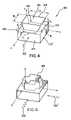
- FIG. 4depicts an antenna according to another embodiment of the invention.
- Antenna 400comprises radiating element 405 coupled to waveguide 410 , over coupling port 440 .
- the radiating element 405has generally a polygon cross-section.
- the height h e of the element 405may be selected as in the previous embodiments, e.g., 0.25 ⁇ .
- the bottom width w L of the elementdetermines the coupling efficiency of the element, while the bottom length L L defines the lowest frequency at which the antenna can operate at.
- the area of the radiating aperture 445i.e., w u ⁇ L u defines the gain of the antenna.
- the angle ⁇defines the beam's shape and may be 90° or less.
- wave 420having a first polarization, enters via the single excitation port 415 .
- another excitation portmay be provided, for example, instead of cavity boundary 415 ′.
- a second wavemay be coupled, having an orthogonal polarization to wave 420 .
- FIG. 5depicts another embodiment of an antenna according to the subject invention.
- the embodiment of FIG. 5is optimized for operation at two orthogonal polarizations.
- the radiating element 505has a cross-section in the shape of a cross that is formed by two superimposed rectangles. In this manner, one rectangle is optimized for radiating wave 520 , while the other rectangle is optimized for radiating wave 520 ′.
- Waves 520 and 520 ′have orthogonal linear polarization.
- the two superimposed rectangles forming the cross-shapehave the same length, so as to operate two waves of similar frequency, but cross-polarization.
- FIG. 6illustrates an embodiment optimized for operation at two different frequencies and optionally two different polarizations.
- the radiating element of FIG. 6has a cross-section in the shape of a cross formed by superimposed rectangles having different lengths. That is, length L 1 is optimized for operation in the frequency of wave 620 , while wave L 2 is optimized for operation at frequency of wave 620 ′. Waves 620 and 620 ′ may be cross-polarized.
- the intersecting waveguides forming the crossmay also be constructed using a centrally located ridge in each waveguide, with the dimensional parameters of the ridge along with L 1 and L 2 optimized to provide broadband frequency operation.
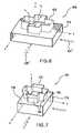
- FIG. 7depicts an embodiment of the invention using a radiating element 705 having flared sidewalls.
- Each elementcomprises a lower perpendicular section and an upper flared section.
- the sides 702 of the perpendicular sectiondefine planes which are perpendicular to the upper surface 730 of the waveguide 710 , where the coupling aperture (not shown) is provided.
- the sides 704 of the flared sectiondefine planes which are angularly offset from, and non-perpendicular to the plane defined by the upper surface 730 of the waveguide 710 .
- the element 705 of FIG. 7is similar to the elements shown in FIGS. 5 and 6 , in that it is optimized for operating with two waves having similar or different frequencies and optionally at cross polarization. However, by introducing the flare on the sidewalls, the design of the coupling aperture can be made independently of the design of the radiating aperture. This is similar to the case illustrated in the previous embodiments where the sidewalls are provided at an angle ⁇ less than 90°.
- wide band capabilitiesmay be provided by a wideband XPD (cross polar discrimination), circular polarization element.
- a wideband XPDcross polar discrimination
- One difficulty in generating a circular polarization waveis the need for a complicated feed network using hybrids, or feeding the element from two orthogonal points. Another possibility is using corner-fed or slot elements. Current technology using these methods negatively impacts the bandwidth needed for good cross-polarization performance, as well as the cost and complexity of the system.
- Alternate solutions usually applied in waveguide antennase.g., horns
- an external polarizere.g., metallic or dielectric
- FIG. 8Adepicts an embodiment of an antenna 800 optimized for circularly polarized radiation. That is, when a planar wave 820 is fed to the waveguide 810 , upon coupling to the radiating element 805 slots 890 would introduce a phase shift to the planar wave so as to introduce circular polarization so that the radiating wave would be circularly polarized. As shown, the slots 890 are provided at 45° alignments to the excitation port 815 . Consequently, if a second planar wave, 820 ′ is introduced via port 815 ′, the radiating element 805 would produce two wave of orthogonal circular polarization.
- FIG. 8Bis a top view of the embodiment of FIG. 8A .
- the following polarization control schemeis presented.
- a planar waveis generated and caused to propagate in the waveguide's cavity, as shown by arrow Vt.
- a circular polarizationis introduced to the planar wave by perturbing the cone element's fields and introducing a phase shift of 90 degrees between the two orthogonal E field components (e.g., the components that are parallel to the slot and the components that are perpendicular to the slot Vx, Vy). This creates a circularly polarized field. This is accomplished without effecting the operation of the array into which the circular polarization element is incorporated.
- the perturbationis in a 45 degree relationship to the polarized field that is propagating in the cavity just beneath the element.
- FIG. 8Cdepicts another embodiment of an antenna optimized for circularly polarized radiation.
- the thickness of the slotshould be sufficiently large so as to cause the perturbation in the wave. It is recommended to be in the order of 0.05-0.1 ⁇ .
- the size of the slots and the area A delimited between themshould be such that the effective dielectric constant generated is higher than that of the remaining area of the radiating element, so that the component Vy propagates at a slower rate than the component Vx, to thereby provide a circularly polarized wave of Vx+jVy.
- FIG. 8Cdepicts another embodiment of an antenna optimized for circularly polarized radiation.
- FIG. 8Cdepicts another embodiment of an antenna optimized for circularly polarized radiation.
- the radiating element 805is a cone similar to that of the embodiment of FIG. 1A .
- a retarder 891 in the form of a piece of material, e.g. Teflon, having higher dielectric constant than airis inserted to occupy an area similar to that of the slots and area A of FIG. 8B .
- FIG. 8Dillustrate a top view of a square circularly polarizing radiating element
- FIG. 8Eillustrates a top view of a cross-shaped circularly polarizing radiating element.
- Some advantages of this featuremay include, without limitation: (1) an integrated polarizer; (2) cross polar discrimination (XPD) greater than 30 dB; (3) adaptability to a relatively flat antenna; (4) very low cost; (5) simple control; (6) wideband operation; and (6) the ability to be excited to generate simultaneous dual polarization.
- Some adaptations of this featureinclude, without limitation: (1) a technology platform for any planar antenna needing a circular polarization wideband field; (2) DBS fixed and mobile antennas; (3) VSAT antenna systems; and (4) fixed point-to-point and point-to-multipoint links.
- FIG. 9illustrates a linear antenna array according to an embodiment of the invention.
- the linear arrayhas 1 ⁇ m radiating element, where in this example 1 ⁇ 3 array is shown.
- radiating elements 905 1 , 905 2 , and 905 3are provided on a single waveguide 910 .
- cone-shaped radiating elementsare used, but any shape can be used, including any of the shapes disclosed above.
- FIG. 10provides a cross-section of the embodiment of FIG. 9 .
- the wave 1020propagates inside the cavity of waveguide 1010 in direction Vt, and part of its energy is coupled to each of the radiating elements as in the previous embodiments.
- each radiating elementcan be controlled by the geometry, as explained above with respect to a single element. Also, as explained above, the distance Ly from the back of the cavity to the last element in the array should be configured so that a reflective wave, if any, would be reflected in phase with the traveling wave. If each radiating element couples sufficient amount of energy so that no energy is left to reflect from the back of the cavity, then the resulting configuration provides a traveling wave. If, on the other hand, some energy remains and it is reflected in phase from the back of the cavity, a standing wave results.
- FIG. 11illustrates a linear array 1100 fed by a sectoral horn 1190 as a source, according to an embodiment of the invention.
- rectangular radiating elements 1105are used, although other shapes may be used.
- the feedis provided using an H-plan sectoral horn 1190 , but other means may be used for wave feed.
- the spacing Spcan be used to introduce a static tilt to the beam.
- a linear arraymay be constructed using radiating elements incorporating any of the shapes disclosed herein, such as conical, rectangular, cross-shaped, etc.
- the shape of the array elementsmay be chosen, at least in part, on the desired polarization characteristics, frequency, and radiation pattern of the antenna.
- the number, distribution and spacing of the elementsmay be chosen to construct an array having specific characteristics, as will be explained further below.
- FIG. 12Aillustrates an example of a two-dimensional array 1200 according to an embodiment of the invention.
- the array of FIG. 12Ais constructed by a waveguide 1210 having an n ⁇ m radiating elements 1205 .
- the resulting arrayis a linear array.
- the radiating elementsmay be of any shape designed so as to provide the required performance.
- the array of FIG. 12Amay be used for polarized radiation and may also be fed from two orthogonal directions to provide a cross-polarization, as explained above. Also, by providing proper feeding, beam steering and the generation of multiple simultaneous beams can be enabled, as will be explained below.
- the example of the rectangular cone array antenna 1200 shown in FIG. 12Ais a based on the use of a cone element 1205 as the basic component of the array.
- the antenna 1200is being excited by a plane wave source 1208 , which may be formed as a slotted waveguide array, microstrip, or any other feed, and having a feed coupler 1295 (e.g. coaxial connector).
- a slotted waveguide array feedis used and the slots on the feed 1208 (not shown), are situated on the wider dimension of the waveguide 1210 , thus exciting a vertical polarized plane wave.
- the wavethen propagates into the cavity, where on the top surface 1230 of the cavity the cone elements 1205 are situated on a rectangular grid of designed fixed spacing along the X and Y dimensions.
- the spacingis calculated to either provide a boresignt radiation or tilted radiation.
- Each cone 1205couple a portion of the energy of the propagating wave, and excite the upper aperture of the cone 1205 , once the wave has reached all the cones in the array, each of the cones function as a source for the far field of the antenna.
- Pencil Beam radiation patternIn the far field of the antenna, one gets a Pencil Beam radiation pattern, with a gain value that is proportional to the number of elements in the array, the spacing between them, and related to the amplitude and phase of their excitations.
- the wave energyis coupled to the array without the need to elaborate waveguide network.
- an array of 4 ⁇ 4 elementswould require a waveguide network having 16 individual waveguides arranged in a manifold leading to the port.
- the feeding networkis eliminating by coupling the wave energy directly from the cavity to the radiating elements.
- FIG. 12Billustrates a two-dimensional array according to another embodiment of the invention configured for operation with two sources.
- FIG. 12Cis a top view of the array illustrated in FIG. 12B .
- the waveguide base and radiating elementsare the same as in FIG. 12A , except that two faces of the waveguide are provided with sources 1204 and 1206 .
- sources 1204 and 1206are provided, but other sources may be used.
- source 1204radiates a wave having vertical polarization, as exemplified by arrows 1214 .
- the waveassumes a horizontal polarization in the Y direction, as exemplified by arrows 1218 .
- source 1206radiates a planar wave, which is also vertically polarized, however upon coupling to the radiating elements assumes a horizontal polarization in the X direction. Consequently, the antenna array of FIG. 12B can operate at two cross polarization radiations. Moreover, each source 1204 and 1206 may operate at different frequency.
- Each of sources 1204 and 1206is constructed of a pin source 1224 and 1226 and a curved reflector 1234 and 1236 .
- the curve of the reflectorsis designed to provide the required planar wave to propagate into the cavity of the waveguide.
- Focusing reflectors 1254 and 1256are provided to focus the transmission from the pins 1204 and 1206 towards the curved reflectors 1234 and 1236 .
- a circular array antennacan be constructed using a circular waveguide base and radiating elements of any of the shapes disclosed herein.
- the circular array antennamay also be characterized as a “flat reflector antenna.”
- high antenna efficiencyhas not been provided in a 2-D structure. High efficiencies can presently only be achieved in offset reflector antennas (which are 3-D structures).
- the 3-D structuresare bulky and also only provide limited beam scanning capabilities. Other technologies such as phased arrays or 2-D mechanical scanning antennas are typically large and expensive, and have low reliability.
- the circular array antenna described hereinprovides a low-cost, easily manufactured antenna, which enables built-in scanning capabilities over a wide range of scanning angles. Accordingly, a circular cavity waveguide antenna is provided having high aperture efficiency by enabling propagation of electromagnetic energy through air within the antenna elements (the cross sections of which can be cones, crosses, rectangles, other polygons, etc.).
- the elementsare situated and arranged on the constant phase curves of the propagating wave. In the case of a cylindrical cavity reflector, the elements are arranged on pseudo arcs.
- the cavity back wall cross-section functionparabolic shape or other
- the structuremay be fed by a cylindrical pin (e.g., monopole type) source that generates a cylindrical wave.
- a cylindrical pine.g., monopole type
- the conescouple the energy at each point along the constant phase curves, and by carefully controlling the cone radii and height, one can control the amount of energy coupled, changing both the phase and amplitude of the field at the aperture of the cone. Similar mechanism can be applied to any shape of element.
- FIG. 13illustrates and example of a circular array antenna 1300 according to an embodiment of the invention.
- the base of the antennais a circularly-shaped waveguide 1310 .
- a plurality of radiating elements 1305are arranged on top of the waveguide.
- the cone-shaped radiating elementsare used, but other shapes may also be used, including the circular-polarization inducing elements.
- the radiating elements 1305are arranged in arcs about a central axis. The shape of the arcs depends on the feed and the desired characteristics of radiation.
- the antennais fed by an omni-directional feed, in this case a single metallic pin 1395 placed at the edge of the plate, which is energize by a coaxial cable 1390 , e.g.
- a 50′ ⁇ coaxial lineThis feed generates a cylindrical wave that propagates inside the cavity.
- the radiating elements 1305are arranged along fixed-phase arcs so as to couple the energy of the wave and radiate it to the air. Since the wave in the waveguide propagates in free space and is coupled directly to the radiating elements, there is very little insertion loss. Also, since the wave is confined to the circular cavity, most of the energy can be used for radiation if the elements are carefully placed. This enables high gain and high efficiency of the antenna well in excess of that achieved by other flat antenna embodiments and offset reflector antennas.
- FIG. 14is a top view of another embodiment of a circular array antenna 1400 of the invention.
- This embodimentalso uses a circular waveguide 1410 , but the radiating elements 1405 are arranged in different shape arcs, which are symmetrical about the central axis.
- the feedmay also be in the form of a pin 1495 provided at the edge of the axis, defining the boresight.
- the various array antennascan enable beam scanning.
- the sourcein order to scan the beam of a circular waveguide the source can be placed in different angular locations along the circumference of the circular cavity, thus creating a phase distribution along previously constant phase curves. At each curve there will be a linear phase distribution in both the X and Y directions, which in turn will tilt the beam in the Theta and Phi directions.
- Thisachieves an efficient thin, low-cost, built-in scanning antenna array.
- Arranging a set of feeds located on an arcenables a multi-beam antenna configuration, which simplifies beam scanning without the need for typical phase shifters.
- Some advantages of this aspect of the inventionmay include, without limitation: (1) a 2-D structure which is flat and thin; (2) extremely low cost and low mechanical tolerances fit for mass production; (3) built-in reflector and feed arrangement, which enables wide-beam scanning without the need for expensive phase shifters or complicated feeding networks; (4) scalable to any frequency; (5) can work in multi-frequency operation such as two-way or one-way applications; (6) can accommodate high-power applications.
- Some associated applicationsmay include, without limitation: (1) one-way DBS mobile or fixed antenna system; (2) two-way mobile IP antenna system (3) mobile, fixed, and/or military SATCOM applications; (4) point-to-point or point-to-multipoint high frequency (up to approximately 100 GHz) band systems; (5) antennas for cellular base stations; (6) radar systems.
- FIG. 15illustrates a process of designing an array according to an embodiment of the invention.
- the parameters desired gain, G, efficiency, ⁇ , and frequency, f 0are provided as input into the gain equation to obtain the required effective area Aeff.
- the desired static tilt angles ( ⁇ 0 x, ⁇ 0 y) of the beam along y and x directionare provide as input, so as to determine the spacing of the elements along the x and y directions (see description relating to FIG. 10 ).
- the beamcan be statically tilted to any direction in (r, ⁇ ) space.
- Step 1535if the radiating element chosen is circular, the lower radius is determined at Step 1540 , i.e., the radius of the coupling aperture, and using the height determined at Step 1545 (e.g., 0.3 ⁇ ) the upper radius, i.e., the radiating aperture, is generated at Step 1550 .
- the lower radius and length of the elementi.e., the area of the coupling aperture, are determined.
- the heightis selected based on the wavelength at step 1565 . If flare is desired, the upper width and length may be tuned to obtain the proper characteristics as desired.
- a rectangular metal waveguideis used as the base for the antenna.
- the radiating element(s)may be formed by extrusion on a side of the waveguide.
- Each radiating elementmay be open at its top to provide the radiating aperture and at the bottom to provide the coupling aperture, while the sides of the element comprise metal extruded from the waveguide.
- Energy traveling within the waveguideis radiated through the element and outwardly from the element through the open top of the element.
- the entire waveguide-radiating element(s) structureis made of plastic using any conventional plastic fabrication technique, and is then coated with metal. In this way a simple manufacturing technique provides an inexpensive and light antenna.
- An advantage of the array designis the relatively high efficiency (up to about 80-90% efficiency in certain situations) of the resulting antenna.
- the wavespropagate through free space and the extruded elements do not require great precision in the manufacturing process.
- the antenna costsare relatively low.
- the radiating elements of the subject inventionneed not be resonant thus their dimensions and tolerances may be relaxed.
- the open waveguide elementsallow for wide bandwidth and the antenna may be adapted to a wide range of frequencies.
- the resulting antennamay be particularly well-suited for high-frequency operation. Further, the resulting antenna has the capability for an end-fire design, thus enabling a very efficient performance for low-elevation beam peaks.
- a number of wave sourcesmay be incorporated into any of the embodiments of the inventive antenna.
- a linear phased array micro-strip antennamay be incorporated.
- the phase of the planar wave exciting the radiating arraycan be controlled, and thus the main beam orientation of the antenna may be changed accordingly.
- a linear passive switched Butler matrix array antennamay be incorporated.
- a passive linear phased arraymay be constructed using Butler matrix technology.
- the different beamsmay be generated by switching between different inputs to the Butler matrix.
- a planar waveguide reflector antennamay be used. This feed may have multi-feed points arranged about the focal point of the planar reflector to control the beam scan of the antenna.
- the multi-feed pointscan be arranged to correspond to the satellites selected for reception in a stationary or mobile DBS system.
- the reflectormay have a parabolic curve design to provide a cavity confined structure.
- one-dimensional beam steeringis achieved (e.g., elevation) while the other dimension (e.g., azimuth beam steering) is realized by rotation of the antenna, if required.
- the subject inventionprovides advantageous feed mechanisms that may be used in conjunction with the various inventive radiating elements described herein, or in conjunction with a conventional antenna using, e.g., micro-strip array, slotted cavity, or any other conventional radiating elements. Since the type of radiating elements used in conjunction with the innovative feed mechanism is not material, the radiating elements will not be explicitly illustrated in some of the figures relating to the feed mechanism, but rather “x” marks will be used instead to illustrate their presence.
- FIG. 16illustrates an embodiment of an RF feed according to an embodiment of the invention.
- a two dimensional array antenna 1600is bounded at sides 1620 , 1625 , and 1630 , to define cavity 1660 , which receives radiation from side 1635 .
- Antenna 1600has a plurality of radiating elements 1605 , the location of each of which is generally indicates by “x”, which may be of any conventional type, or of any of the inventive radiating elements described herein.
- the embodiment of FIG. 16illustrates a single point feed arrangement, so it has a single radiating source and a single beam.
- radiation pin 1615is provided in the area between open (feed) side 1635 and reflector 1610 .
- the radiating pin 1615radiates energy so as to generate a planar wave front at the entry face 1635 to the cavity 1660 , propagating in a direction and with phase and amplitude distribution that is according to the design of the reflector 1610 and the location of the pin.
- the radiation directionis boresight, as shown in FIG. 16 . If the pin is moved to the left along arrow L, the beam would tilt to the right and, conversely, if the pin is moved to the right the beam would tilt to the left. That is, beam tilt may be controlled by the location of the radiating pin. Thus, for example, by mechanically moving the radiating pin, one can control the beam tilt.
- the reflector 1610is made of an RF reflective material, such as metal or plastic coated with metallic layer, and is designed as a function f(x,y) so as to generate the desired beam shape, i.e., aperture, which includes amplitude and phase.
- FIG. 16Aillustrate a reflector that may follow a parabolic or cylindrical function
- FIG. 16Billustrates a reflector that follows a 3-dimensional, toroidal shape.
- an optional counter reflector 1640is used so as to have the radiation from the pin reflected back towards the reflector 1610 , generating a focusing effect. While the counter reflector is not necessary, it provides an improved performance.
- FIG. 16the reflector 1610 is shown extending from one side of the antenna.
- the feeding-reflector arrangementmay be “folded” under the antenna.
- FIGS. 16C and 16DAn example is illustrated in FIGS. 16C and 16D .
- FIG. 16Cillustrate a perspective view from under the antenna, showing the folded feed-reflector arrangement, while FIG. 16D illustrate a cross-section along line A-A of FIG. 16C .
- the feed couplere.g., a coaxial connector 1645
- the transmission linee.g., coaxial cable 1644 .
- This arrangementprovides the same radiation characteristics as that of FIG. 16 , except that the total area of the device is reduced.
- FIG. 16Eillustrates an embodiment of the innovative reflector feed used in conjunction with a patch array.
- the RF cavity 1660is similar to that of FIG. 16 , and similarly has end wall 1630 opposite the curved reflector 1610 .
- a radiation source, such as radiating pin 1615is coupled to a transmission line, e.g., coaxial cable, 1644 via coupler 1645 .
- the top part of the cavity 1660is covered with an insulator 1680 .
- Conductive patches 1605are provided on top of the insulator 1680 , serving as radiating elements. Energy from the cavity 1660 is coupled to the radiating patches via conductive pins 1607 extending from each patch into the cavity 1660 .
- FIG. 17illustrate an embodiment of an RF feed that is similar to that of FIG. 16 , except that multiple RF radiation pins 1715 are used.
- the absolute location of each pindetermines the beam tilt generated by radiation from that pin.
- each pin locationthere is a distinct beam location in space.
- each pin locationwill scan the beam in a plane that is parallel to the axis upon which the pins are arranged. Therefore, if the pins are energized serially, one obtains a beam scan in the direction between sides 1720 and 1725 . On the other hand, one may energize all of the pins simultaneously, resulting in the following.
- one main beam pinis used in conjunction with two or more very close side pins, so as to shape the main beam. This is termed beam shaping.
- the energy to the adjacent beamsis weighted, thereby improving the beam slop and thus improving interference satellite rejection or any other needed rejection, or shape the beam to a desired shape.
- one or more pinsare fed at any given time, each pin corresponding to one beam tilted at a designed angle so as to point to a particular location in the sky, i.e., each pin corresponding to one satellite in the sky.
- FIG. 18illustrate an embodiment having dual-feed arrangement.
- two reflectors 1810 and 1820are used to provide dual polarization radiation into the cavity of array elements 1805 .
- the resulting beamis therefore scanned along the diagonal D as illustrated.
- one sideis fed horizontal polarization and the other vertical polarization, one may generate circularly polarized radiation.
- FIG. 19illustrates the principle of beam tilt/scanning over the diagonal of a symmetrical array 1900 .
- radiating pin 1915generates a plane wave 1917 of horizontal polarization, which propagates into the array as shown by arrow H.
- Radiating pin 1955generates a plane wave 1957 of vertical polarization, which propagates into the array as shown by arrow V.
- a 90 degrees phaseis introduce between the horizontal and vertical polarized waves. This is done prior to feeding the pins 1915 and 1955 by, for example, using a hybrid or other electrical element illustrated generically as D.
- wave fronts arriving at elements that are placed symmetrically about the diagonalare also summed up due to the symmetry.
- the distance traveled by wavefront V to element 1980is d V
- the distance traveled by wave front V to element 1985is 2d V
- the distance traveled by wave front V to element 1985is 2d V
- the radiating elementsshould have a symmetrical geometry, e.g., circular or square, and their distribution over the array should be symmetrical about the diagonal.
- FIGS. 20A and 20Billustrate an embodiment wherein the inventive reflector feed is utilized for an array operating in two frequencies of different bands.
- this arraycan simultaneously operate at two frequencies that are vastly different, for example one at Ka band, while another at Ku band.
- radiating elements 2005are optimized to operate at one frequency, e.g., at Ka band
- radiating elements 2003are optimized to operate at the other frequency, e.g., at Ku band.
- the radiating elements 2005form one array that is symmetrical about diagonal D
- the radiating elements 2003form a second array also symmetrical about diagonal D.
- the radiating elements 2005are fed from reflector feeds 2010 and 2012
- radiating elements 2003are fed from reflector feed 2014 and 2016 . It should be appreciated that in the cross-section image of FIG. 20B the reflector feeds are folded, while in the top elevation of FIG. 20A the reflectors are not folded.
- FIG. 20Cis a basic cross section of the unit cell of the mixed array concept, according to an embodiment of the invention.
- the higher band elements 2005are designed first, so as to have the ability to couple the high band energy propagating inside the waveguide structure 2060 .
- the lower diameter of elements 2005presents frequency cutoff conditions, basically filtering the low frequency energy that propagates inside cavity 2060 without interruption or coupling to elements 2005 .
- the low band elementscan couple and support both the high and low frequency bands, and couple the energy for both bands, thus enabling the use of the whole area for the higher band, and the use of only the lower frequency array for the lower band.
- the height h HB of the cavity 2060 at the area where the high band elements are providedis designed for the frequency at the high band, while the height h LB of the cavity 2060 is higher and designed according to the frequency of the low band.
- the distance between elements, dx HBis designed to be equal or lower than the high band wavelength ⁇ g HB
- the length dx LBis designed to be equal or lower than the low band wavelength ⁇ g LB , wherein ⁇ g corresponds to the wavelength ⁇ 0 as transformed in the cavity 2060 .
- the diameter d r , of the opening of the high band cones 2005are designed to present a short for the wavelength of the low band, thereby operating as a cutoff or filter.
- both high band array and low band arrayare square arrays that can produce a standard radiation pattern.
- the low frequency band gain and radiation patternsare governed only by the low frequency band array, but the high band gain and radiation pattern and frequency beam scanning is governed by both the high band and low band arrays and is weighted by controlling the spacing and cone size on both the high and low band arrays. In fact by doing so we mitigate the frequency scanning effects on the high band.
- FIGS. 20D and 20Eillustrate variations for the reflector feeds for the mixed array concept.
- the feed for both the high band and low bandis done from the same side, i.e., reflector feed 2010 is used for both high and low bands for one polarization, while reflector feed 2012 is used for both high and low bands for the other polarization.
- FIG. 20Eillustrate symmetrical reflector feeding arrangement, wherein the same size reflector feeds are provided about all four corners of the array.
- the location of the RF source with respect to the reflectordetermines the tilt of the beam. Therefore, one may use different sources at different locations to have beams tilted at different angles. For example, in FIG. 20D five sources, here in the form of pins, are used so have the array point to five different satellites. The sources and the distances between them are designed so that, in this example, the array may be used for digital television transmission using SAT 99 , SAT 101 (at boresight), SAT 103 , SAT 110 , and SAT 119 .
- FIG. 20 Fillustrates a flow chart for the design of a mixed array antenna.
- the radiating elements for the high and low bandsare designed according to the design embodiment described above.
- the spacing of the high and low band elementsare determined so as to provide maximum efficiency.
- fine-tuningis done in favor of the high band.
- the high band radiation patternis a superposition of the pattern generated by the high band array and the low band array.
- the low band arraygenerates a grating lobe pattern in the high band, that is summed up with the pattern generated by the high band array and helps reduce the frequency scanning effect.
- the design and layoutis then finalized by providing the reflector or other type of RF feed.
- FIGS. 21A and 21Billustrate another embodiment of the invention enabling simultaneous dual polarization with wide-angle reception in one direction with a very short but wide form factor which presents a small form factor for the human eye.
- the antenna of FIGS. 21A and 21Bis beneficial in that it can be easily attached inconspicuously and need not be aimed precisely.
- the antenna of FIGS. 21A and 21Bmay beneficially utilize circularly polarizing elements such as, for example, the one illustrated in FIG. 8C , in conjunction with the inventive reflector feed. In this example, two long antennas 2100 and 2101 are made abutting each other.
- Antenna 2100utilizes elements 2105 which provide, e.g., right hand circular polarization (RHCP), while antenna 2101 utilizes elements 2103 which provide counter circular polarization, i.e., left hand circular polarization (LHCP).
- Antenna 2100utilizes reflector feed 2110 with radiating pin 2117
- antenna 2101utilizes reflector feed 2112 with radiating pin 2115 .
- FIG. 21Athe reflector feed is shown extending from the side of the antennas, while in FIG. 21B the reflector feed is folded.
- FIG. 22illustrates an example of a reflector feed using a horn as an RF source.
- the arrayis constructed using a cavity 2260 having an insulating layer 2280 provided on its top, and patch radiating elements 2205 are provided on top of the insulating layer.
- the cavity 2260is fed by reflector feed 2210 having a horn 2215 as an RF radiating source.
- the horn 2215is fed with an RF energy by RF source 2245 in a conventional manner.
- FIG. 23illustrates an example of a patch radiation source which may be used with the reflector feed of the invention.
- the path feed of FIG. 23may be used in any reflector feed constructed according to the invention.
- the patch radiation source of FIG. 23is constructed of an insulating substrate 2310 having a conductive patch 2305 provided on one face thereof. The path is fed by a conductive trace 2325 .
- the patch radiation sourceis affixed to the antenna so that the conductive patch faces the reflector.
- a conductive layer 2320is provided on the backside of the substrate 2310 . This functions to prevent any radiation from the patch to propagate directly into the cavity. In essence the conductive layer 2320 functions similarly to the counter reflector of FIG. 16 .
- an antenna systemmay be integrated into a mobile platform such as an automobile. Because the platform is moving and existing satellite systems are fixed with respect to the earth (geostationary), the receiving antenna should be able to track a signal coming from a satellite.
- a beam steering mechanismis preferably built into the system.
- the beam steering elementallows coverage over a two-dimensional, hemispherical space.
- a one-dimensional electrical scane.g., phased array or switched feeds
- mechanical rotationmay be used.
- the walls of a plurality of radiating elementsmay be mechanically rotated (e.g., by a motor) over a range of angles defined by the element wall in relation to the non-extruded surface of the waveguide.
- the rotationmay be achieved for a range of angles to achieve a 360 degree azimuth range and an elevation range of from about 20-70 degrees.
- a two-dimensional lens scanmay be incorporated.
- the antenna arraymay be designed to radiate at a fixed angle and a lens may be situated to interfere with the radiation.
- the lensis situated outwardly from the radiating elements.
- the lenshas a saw-tooth configuration.
- a radiated beammay be steered in a certain direction by controlling the movement of the lens.
- Superimposition of another lens orthogonal to the firstmay allow two-dimensional scanning.
- onemay use an irregularly shaped lens (which provides the equivalent of the movement of the two separate lenses) and then rotate the irregular lens to achieve two-dimensional scanning.
- Some advantages of the inventionmay include, without limitation: (1) a two-dimensional structure which is flat and thin; (2) potential for extremely low cost and low mechanical tolerances fit for mass production; (3) built-in reflector and feed arrangement, which enables wide beam scanning without the need for expensive phase shifters or complicated feeding networks; (4) scalable to any frequency; (5) capability for multi-frequency operation in both two-way or one-way applications; (6) ability to accommodate high-power applications because of the simple low-loss structure with the absence of small dimension gaps.
- Some associated applicationsmay include, without limitation: (1) one-way DBS mobile or fixed antenna system; (2) two-way mobile IP antenna system (3) mobile, fixed, and/or military SATCOM applications; (4) point-to-point or point-to-multipoint high frequency (up to approximately 100 GHz) band systems; (5) antennas for cellular base stations; (6) radar systems.
Landscapes
- Variable-Direction Aerials And Aerial Arrays (AREA)
- Waveguide Aerials (AREA)
- Aerials With Secondary Devices (AREA)
Abstract
Description
Claims (20)
Priority Applications (2)
| Application Number | Priority Date | Filing Date | Title |
|---|---|---|---|
| US11/931,610US7656358B2 (en) | 2006-05-24 | 2007-10-31 | Antenna operable at two frequency bands simultaneously |
| PCT/US2007/024027WO2008069908A2 (en) | 2006-11-17 | 2007-11-16 | An antenna operable at two frequency bands simultaneously |
Applications Claiming Priority (6)
| Application Number | Priority Date | Filing Date | Title |
|---|---|---|---|
| US80818706P | 2006-05-24 | 2006-05-24 | |
| US85979906P | 2006-11-17 | 2006-11-17 | |
| US85966706P | 2006-11-17 | 2006-11-17 | |
| US89045607P | 2007-02-16 | 2007-02-16 | |
| US11/695,913US7466281B2 (en) | 2006-05-24 | 2007-04-03 | Integrated waveguide antenna and array |
| US11/931,610US7656358B2 (en) | 2006-05-24 | 2007-10-31 | Antenna operable at two frequency bands simultaneously |
Related Parent Applications (1)
| Application Number | Title | Priority Date | Filing Date |
|---|---|---|---|
| US11/695,913Continuation-In-PartUS7466281B2 (en) | 2006-05-24 | 2007-04-03 | Integrated waveguide antenna and array |
Publications (2)
| Publication Number | Publication Date |
|---|---|
| US20080111755A1 US20080111755A1 (en) | 2008-05-15 |
| US7656358B2true US7656358B2 (en) | 2010-02-02 |
Family
ID=39492791
Family Applications (1)
| Application Number | Title | Priority Date | Filing Date |
|---|---|---|---|
| US11/931,610Expired - Fee RelatedUS7656358B2 (en) | 2006-05-24 | 2007-10-31 | Antenna operable at two frequency bands simultaneously |
Country Status (2)
| Country | Link |
|---|---|
| US (1) | US7656358B2 (en) |
| WO (1) | WO2008069908A2 (en) |
Cited By (138)
| Publication number | Priority date | Publication date | Assignee | Title |
|---|---|---|---|---|
| US20080303739A1 (en)* | 2007-06-07 | 2008-12-11 | Thomas Edward Sharon | Integrated multi-beam antenna receiving system with improved signal distribution |
| US20100149061A1 (en)* | 2008-12-12 | 2010-06-17 | Haziza Dedi David | Integrated waveguide cavity antenna and reflector dish |
| US9236652B2 (en) | 2012-08-21 | 2016-01-12 | Raytheon Company | Broadband array antenna enhancement with spatially engineered dielectrics |
| US9667317B2 (en) | 2015-06-15 | 2017-05-30 | At&T Intellectual Property I, L.P. | Method and apparatus for providing security using network traffic adjustments |
| US9674711B2 (en) | 2013-11-06 | 2017-06-06 | At&T Intellectual Property I, L.P. | Surface-wave communications and methods thereof |
| US9685992B2 (en) | 2014-10-03 | 2017-06-20 | At&T Intellectual Property I, L.P. | Circuit panel network and methods thereof |
| US9705610B2 (en) | 2014-10-21 | 2017-07-11 | At&T Intellectual Property I, L.P. | Transmission device with impairment compensation and methods for use therewith |
| US9705561B2 (en) | 2015-04-24 | 2017-07-11 | At&T Intellectual Property I, L.P. | Directional coupling device and methods for use therewith |
| US9722318B2 (en) | 2015-07-14 | 2017-08-01 | At&T Intellectual Property I, L.P. | Method and apparatus for coupling an antenna to a device |
| US9729197B2 (en) | 2015-10-01 | 2017-08-08 | At&T Intellectual Property I, L.P. | Method and apparatus for communicating network management traffic over a network |
| US9735833B2 (en) | 2015-07-31 | 2017-08-15 | At&T Intellectual Property I, L.P. | Method and apparatus for communications management in a neighborhood network |
| US9742462B2 (en) | 2014-12-04 | 2017-08-22 | At&T Intellectual Property I, L.P. | Transmission medium and communication interfaces and methods for use therewith |
| US9742521B2 (en) | 2014-11-20 | 2017-08-22 | At&T Intellectual Property I, L.P. | Transmission device with mode division multiplexing and methods for use therewith |
| US9749013B2 (en) | 2015-03-17 | 2017-08-29 | At&T Intellectual Property I, L.P. | Method and apparatus for reducing attenuation of electromagnetic waves guided by a transmission medium |
| US9749053B2 (en) | 2015-07-23 | 2017-08-29 | At&T Intellectual Property I, L.P. | Node device, repeater and methods for use therewith |
| US9748626B2 (en) | 2015-05-14 | 2017-08-29 | At&T Intellectual Property I, L.P. | Plurality of cables having different cross-sectional shapes which are bundled together to form a transmission medium |
| US9769020B2 (en) | 2014-10-21 | 2017-09-19 | At&T Intellectual Property I, L.P. | Method and apparatus for responding to events affecting communications in a communication network |
| US9768833B2 (en) | 2014-09-15 | 2017-09-19 | At&T Intellectual Property I, L.P. | Method and apparatus for sensing a condition in a transmission medium of electromagnetic waves |
| US9769128B2 (en) | 2015-09-28 | 2017-09-19 | At&T Intellectual Property I, L.P. | Method and apparatus for encryption of communications over a network |
| US9780834B2 (en) | 2014-10-21 | 2017-10-03 | At&T Intellectual Property I, L.P. | Method and apparatus for transmitting electromagnetic waves |
| US9787412B2 (en) | 2015-06-25 | 2017-10-10 | At&T Intellectual Property I, L.P. | Methods and apparatus for inducing a fundamental wave mode on a transmission medium |
| US9793954B2 (en) | 2015-04-28 | 2017-10-17 | At&T Intellectual Property I, L.P. | Magnetic coupling device and methods for use therewith |
| US9793951B2 (en) | 2015-07-15 | 2017-10-17 | At&T Intellectual Property I, L.P. | Method and apparatus for launching a wave mode that mitigates interference |
| US9793955B2 (en) | 2015-04-24 | 2017-10-17 | At&T Intellectual Property I, Lp | Passive electrical coupling device and methods for use therewith |
| US9800327B2 (en) | 2014-11-20 | 2017-10-24 | At&T Intellectual Property I, L.P. | Apparatus for controlling operations of a communication device and methods thereof |
| US9820146B2 (en) | 2015-06-12 | 2017-11-14 | At&T Intellectual Property I, L.P. | Method and apparatus for authentication and identity management of communicating devices |
| US9838896B1 (en) | 2016-12-09 | 2017-12-05 | At&T Intellectual Property I, L.P. | Method and apparatus for assessing network coverage |
| US9838078B2 (en) | 2015-07-31 | 2017-12-05 | At&T Intellectual Property I, L.P. | Method and apparatus for exchanging communication signals |
| US9847566B2 (en) | 2015-07-14 | 2017-12-19 | At&T Intellectual Property I, L.P. | Method and apparatus for adjusting a field of a signal to mitigate interference |
| US9847850B2 (en) | 2014-10-14 | 2017-12-19 | At&T Intellectual Property I, L.P. | Method and apparatus for adjusting a mode of communication in a communication network |
| US9853342B2 (en) | 2015-07-14 | 2017-12-26 | At&T Intellectual Property I, L.P. | Dielectric transmission medium connector and methods for use therewith |
| US9860075B1 (en) | 2016-08-26 | 2018-01-02 | At&T Intellectual Property I, L.P. | Method and communication node for broadband distribution |
| US9866309B2 (en) | 2015-06-03 | 2018-01-09 | At&T Intellectual Property I, Lp | Host node device and methods for use therewith |
| US9865911B2 (en) | 2015-06-25 | 2018-01-09 | At&T Intellectual Property I, L.P. | Waveguide system for slot radiating first electromagnetic waves that are combined into a non-fundamental wave mode second electromagnetic wave on a transmission medium |
| US9866276B2 (en) | 2014-10-10 | 2018-01-09 | At&T Intellectual Property I, L.P. | Method and apparatus for arranging communication sessions in a communication system |
| US9871282B2 (en) | 2015-05-14 | 2018-01-16 | At&T Intellectual Property I, L.P. | At least one transmission medium having a dielectric surface that is covered at least in part by a second dielectric |
| US9871558B2 (en) | 2014-10-21 | 2018-01-16 | At&T Intellectual Property I, L.P. | Guided-wave transmission device and methods for use therewith |
| US9871283B2 (en) | 2015-07-23 | 2018-01-16 | At&T Intellectual Property I, Lp | Transmission medium having a dielectric core comprised of plural members connected by a ball and socket configuration |
| US9876571B2 (en) | 2015-02-20 | 2018-01-23 | At&T Intellectual Property I, Lp | Guided-wave transmission device with non-fundamental mode propagation and methods for use therewith |
| US9876264B2 (en) | 2015-10-02 | 2018-01-23 | At&T Intellectual Property I, Lp | Communication system, guided wave switch and methods for use therewith |
| US9876605B1 (en) | 2016-10-21 | 2018-01-23 | At&T Intellectual Property I, L.P. | Launcher and coupling system to support desired guided wave mode |
| US9882257B2 (en) | 2015-07-14 | 2018-01-30 | At&T Intellectual Property I, L.P. | Method and apparatus for launching a wave mode that mitigates interference |
| US9887447B2 (en) | 2015-05-14 | 2018-02-06 | At&T Intellectual Property I, L.P. | Transmission medium having multiple cores and methods for use therewith |
| US9893795B1 (en) | 2016-12-07 | 2018-02-13 | At&T Intellectual Property I, Lp | Method and repeater for broadband distribution |
| US9906269B2 (en) | 2014-09-17 | 2018-02-27 | At&T Intellectual Property I, L.P. | Monitoring and mitigating conditions in a communication network |
| US9904535B2 (en) | 2015-09-14 | 2018-02-27 | At&T Intellectual Property I, L.P. | Method and apparatus for distributing software |
| US9912381B2 (en) | 2015-06-03 | 2018-03-06 | At&T Intellectual Property I, Lp | Network termination and methods for use therewith |
| US9911020B1 (en) | 2016-12-08 | 2018-03-06 | At&T Intellectual Property I, L.P. | Method and apparatus for tracking via a radio frequency identification device |
| US9912027B2 (en) | 2015-07-23 | 2018-03-06 | At&T Intellectual Property I, L.P. | Method and apparatus for exchanging communication signals |
| US9912033B2 (en) | 2014-10-21 | 2018-03-06 | At&T Intellectual Property I, Lp | Guided wave coupler, coupling module and methods for use therewith |
| US9913139B2 (en) | 2015-06-09 | 2018-03-06 | At&T Intellectual Property I, L.P. | Signal fingerprinting for authentication of communicating devices |
| US9917341B2 (en) | 2015-05-27 | 2018-03-13 | At&T Intellectual Property I, L.P. | Apparatus and method for launching electromagnetic waves and for modifying radial dimensions of the propagating electromagnetic waves |
| US9929755B2 (en) | 2015-07-14 | 2018-03-27 | At&T Intellectual Property I, L.P. | Method and apparatus for coupling an antenna to a device |
| US9927517B1 (en) | 2016-12-06 | 2018-03-27 | At&T Intellectual Property I, L.P. | Apparatus and methods for sensing rainfall |
| US9948333B2 (en) | 2015-07-23 | 2018-04-17 | At&T Intellectual Property I, L.P. | Method and apparatus for wireless communications to mitigate interference |
| US9954287B2 (en) | 2014-11-20 | 2018-04-24 | At&T Intellectual Property I, L.P. | Apparatus for converting wireless signals and electromagnetic waves and methods thereof |
| US9954286B2 (en) | 2014-10-21 | 2018-04-24 | At&T Intellectual Property I, L.P. | Guided-wave transmission device with non-fundamental mode propagation and methods for use therewith |
| US20180123254A1 (en)* | 2016-10-28 | 2018-05-03 | Ke Wu | Single-layered end-fire circularly polarized substrate integrated waveguide horn antenna |
| US9967173B2 (en) | 2015-07-31 | 2018-05-08 | At&T Intellectual Property I, L.P. | Method and apparatus for authentication and identity management of communicating devices |
| US9973416B2 (en) | 2014-10-02 | 2018-05-15 | At&T Intellectual Property I, L.P. | Method and apparatus that provides fault tolerance in a communication network |
| US9973940B1 (en) | 2017-02-27 | 2018-05-15 | At&T Intellectual Property I, L.P. | Apparatus and methods for dynamic impedance matching of a guided wave launcher |
| US9991580B2 (en) | 2016-10-21 | 2018-06-05 | At&T Intellectual Property I, L.P. | Launcher and coupling system for guided wave mode cancellation |
| US9999038B2 (en) | 2013-05-31 | 2018-06-12 | At&T Intellectual Property I, L.P. | Remote distributed antenna system |
| US9997819B2 (en) | 2015-06-09 | 2018-06-12 | At&T Intellectual Property I, L.P. | Transmission medium and method for facilitating propagation of electromagnetic waves via a core |
| US9998870B1 (en) | 2016-12-08 | 2018-06-12 | At&T Intellectual Property I, L.P. | Method and apparatus for proximity sensing |
| US10009067B2 (en) | 2014-12-04 | 2018-06-26 | At&T Intellectual Property I, L.P. | Method and apparatus for configuring a communication interface |
| US10020844B2 (en) | 2016-12-06 | 2018-07-10 | T&T Intellectual Property I, L.P. | Method and apparatus for broadcast communication via guided waves |
| US10027397B2 (en) | 2016-12-07 | 2018-07-17 | At&T Intellectual Property I, L.P. | Distributed antenna system and methods for use therewith |
| US10033107B2 (en) | 2015-07-14 | 2018-07-24 | At&T Intellectual Property I, L.P. | Method and apparatus for coupling an antenna to a device |
| US10033108B2 (en) | 2015-07-14 | 2018-07-24 | At&T Intellectual Property I, L.P. | Apparatus and methods for generating an electromagnetic wave having a wave mode that mitigates interference |
| US10044409B2 (en) | 2015-07-14 | 2018-08-07 | At&T Intellectual Property I, L.P. | Transmission medium and methods for use therewith |
| US10051630B2 (en) | 2013-05-31 | 2018-08-14 | At&T Intellectual Property I, L.P. | Remote distributed antenna system |
| US10069185B2 (en) | 2015-06-25 | 2018-09-04 | At&T Intellectual Property I, L.P. | Methods and apparatus for inducing a non-fundamental wave mode on a transmission medium |
| US10069535B2 (en) | 2016-12-08 | 2018-09-04 | At&T Intellectual Property I, L.P. | Apparatus and methods for launching electromagnetic waves having a certain electric field structure |
| US10090606B2 (en) | 2015-07-15 | 2018-10-02 | At&T Intellectual Property I, L.P. | Antenna system with dielectric array and methods for use therewith |
| US10090594B2 (en) | 2016-11-23 | 2018-10-02 | At&T Intellectual Property I, L.P. | Antenna system having structural configurations for assembly |
| US10103422B2 (en) | 2016-12-08 | 2018-10-16 | At&T Intellectual Property I, L.P. | Method and apparatus for mounting network devices |
| US10129057B2 (en) | 2015-07-14 | 2018-11-13 | At&T Intellectual Property I, L.P. | Apparatus and methods for inducing electromagnetic waves on a cable |
| US10135147B2 (en) | 2016-10-18 | 2018-11-20 | At&T Intellectual Property I, L.P. | Apparatus and methods for launching guided waves via an antenna |
| US10135146B2 (en) | 2016-10-18 | 2018-11-20 | At&T Intellectual Property I, L.P. | Apparatus and methods for launching guided waves via circuits |
| US10135145B2 (en) | 2016-12-06 | 2018-11-20 | At&T Intellectual Property I, L.P. | Apparatus and methods for generating an electromagnetic wave along a transmission medium |
| US10139820B2 (en) | 2016-12-07 | 2018-11-27 | At&T Intellectual Property I, L.P. | Method and apparatus for deploying equipment of a communication system |
| US10148016B2 (en) | 2015-07-14 | 2018-12-04 | At&T Intellectual Property I, L.P. | Apparatus and methods for communicating utilizing an antenna array |
| US10170840B2 (en) | 2015-07-14 | 2019-01-01 | At&T Intellectual Property I, L.P. | Apparatus and methods for sending or receiving electromagnetic signals |
| US10168695B2 (en) | 2016-12-07 | 2019-01-01 | At&T Intellectual Property I, L.P. | Method and apparatus for controlling an unmanned aircraft |
| US10178445B2 (en) | 2016-11-23 | 2019-01-08 | At&T Intellectual Property I, L.P. | Methods, devices, and systems for load balancing between a plurality of waveguides |
| US10205655B2 (en) | 2015-07-14 | 2019-02-12 | At&T Intellectual Property I, L.P. | Apparatus and methods for communicating utilizing an antenna array and multiple communication paths |
| US10224634B2 (en) | 2016-11-03 | 2019-03-05 | At&T Intellectual Property I, L.P. | Methods and apparatus for adjusting an operational characteristic of an antenna |
| US10225025B2 (en) | 2016-11-03 | 2019-03-05 | At&T Intellectual Property I, L.P. | Method and apparatus for detecting a fault in a communication system |
| US10243784B2 (en) | 2014-11-20 | 2019-03-26 | At&T Intellectual Property I, L.P. | System for generating topology information and methods thereof |
| US10243270B2 (en) | 2016-12-07 | 2019-03-26 | At&T Intellectual Property I, L.P. | Beam adaptive multi-feed dielectric antenna system and methods for use therewith |
| US10264586B2 (en) | 2016-12-09 | 2019-04-16 | At&T Mobility Ii Llc | Cloud-based packet controller and methods for use therewith |
| US10291334B2 (en) | 2016-11-03 | 2019-05-14 | At&T Intellectual Property I, L.P. | System for detecting a fault in a communication system |
| US10298293B2 (en) | 2017-03-13 | 2019-05-21 | At&T Intellectual Property I, L.P. | Apparatus of communication utilizing wireless network devices |
| US10305190B2 (en) | 2016-12-01 | 2019-05-28 | At&T Intellectual Property I, L.P. | Reflecting dielectric antenna system and methods for use therewith |
| US10312567B2 (en) | 2016-10-26 | 2019-06-04 | At&T Intellectual Property I, L.P. | Launcher with planar strip antenna and methods for use therewith |
| US10320586B2 (en) | 2015-07-14 | 2019-06-11 | At&T Intellectual Property I, L.P. | Apparatus and methods for generating non-interfering electromagnetic waves on an insulated transmission medium |
| US10326494B2 (en) | 2016-12-06 | 2019-06-18 | At&T Intellectual Property I, L.P. | Apparatus for measurement de-embedding and methods for use therewith |
| US10326689B2 (en) | 2016-12-08 | 2019-06-18 | At&T Intellectual Property I, L.P. | Method and system for providing alternative communication paths |
| US10340573B2 (en) | 2016-10-26 | 2019-07-02 | At&T Intellectual Property I, L.P. | Launcher with cylindrical coupling device and methods for use therewith |
| US10340600B2 (en) | 2016-10-18 | 2019-07-02 | At&T Intellectual Property I, L.P. | Apparatus and methods for launching guided waves via plural waveguide systems |
| US10341142B2 (en) | 2015-07-14 | 2019-07-02 | At&T Intellectual Property I, L.P. | Apparatus and methods for generating non-interfering electromagnetic waves on an uninsulated conductor |
| US10340603B2 (en) | 2016-11-23 | 2019-07-02 | At&T Intellectual Property I, L.P. | Antenna system having shielded structural configurations for assembly |
| US10340601B2 (en) | 2016-11-23 | 2019-07-02 | At&T Intellectual Property I, L.P. | Multi-antenna system and methods for use therewith |
| US10340983B2 (en) | 2016-12-09 | 2019-07-02 | At&T Intellectual Property I, L.P. | Method and apparatus for surveying remote sites via guided wave communications |
| US10355367B2 (en) | 2015-10-16 | 2019-07-16 | At&T Intellectual Property I, L.P. | Antenna structure for exchanging wireless signals |
| US10359749B2 (en) | 2016-12-07 | 2019-07-23 | At&T Intellectual Property I, L.P. | Method and apparatus for utilities management via guided wave communication |
| US10361489B2 (en) | 2016-12-01 | 2019-07-23 | At&T Intellectual Property I, L.P. | Dielectric dish antenna system and methods for use therewith |
| US10374316B2 (en) | 2016-10-21 | 2019-08-06 | At&T Intellectual Property I, L.P. | System and dielectric antenna with non-uniform dielectric |
| US10382976B2 (en) | 2016-12-06 | 2019-08-13 | At&T Intellectual Property I, L.P. | Method and apparatus for managing wireless communications based on communication paths and network device positions |
| US10389029B2 (en) | 2016-12-07 | 2019-08-20 | At&T Intellectual Property I, L.P. | Multi-feed dielectric antenna system with core selection and methods for use therewith |
| US10389037B2 (en) | 2016-12-08 | 2019-08-20 | At&T Intellectual Property I, L.P. | Apparatus and methods for selecting sections of an antenna array and use therewith |
| US10411356B2 (en) | 2016-12-08 | 2019-09-10 | At&T Intellectual Property I, L.P. | Apparatus and methods for selectively targeting communication devices with an antenna array |
| US10439290B2 (en) | 2015-07-14 | 2019-10-08 | At&T Intellectual Property I, L.P. | Apparatus and methods for wireless communications |
| US10439675B2 (en) | 2016-12-06 | 2019-10-08 | At&T Intellectual Property I, L.P. | Method and apparatus for repeating guided wave communication signals |
| US10446936B2 (en) | 2016-12-07 | 2019-10-15 | At&T Intellectual Property I, L.P. | Multi-feed dielectric antenna system and methods for use therewith |
| US10498044B2 (en) | 2016-11-03 | 2019-12-03 | At&T Intellectual Property I, L.P. | Apparatus for configuring a surface of an antenna |
| US10511346B2 (en) | 2015-07-14 | 2019-12-17 | At&T Intellectual Property I, L.P. | Apparatus and methods for inducing electromagnetic waves on an uninsulated conductor |
| US10530505B2 (en) | 2016-12-08 | 2020-01-07 | At&T Intellectual Property I, L.P. | Apparatus and methods for launching electromagnetic waves along a transmission medium |
| US10535928B2 (en) | 2016-11-23 | 2020-01-14 | At&T Intellectual Property I, L.P. | Antenna system and methods for use therewith |
| US10547348B2 (en) | 2016-12-07 | 2020-01-28 | At&T Intellectual Property I, L.P. | Method and apparatus for switching transmission mediums in a communication system |
| US10601494B2 (en) | 2016-12-08 | 2020-03-24 | At&T Intellectual Property I, L.P. | Dual-band communication device and method for use therewith |
| US10637149B2 (en) | 2016-12-06 | 2020-04-28 | At&T Intellectual Property I, L.P. | Injection molded dielectric antenna and methods for use therewith |
| US10650940B2 (en) | 2015-05-15 | 2020-05-12 | At&T Intellectual Property I, L.P. | Transmission medium having a conductive material and methods for use therewith |
| US10694379B2 (en) | 2016-12-06 | 2020-06-23 | At&T Intellectual Property I, L.P. | Waveguide system with device-based authentication and methods for use therewith |
| US10727577B2 (en) | 2018-03-29 | 2020-07-28 | At&T Intellectual Property I, L.P. | Exchange of wireless signals guided by a transmission medium and methods thereof |
| US10727599B2 (en) | 2016-12-06 | 2020-07-28 | At&T Intellectual Property I, L.P. | Launcher with slot antenna and methods for use therewith |
| US10755542B2 (en) | 2016-12-06 | 2020-08-25 | At&T Intellectual Property I, L.P. | Method and apparatus for surveillance via guided wave communication |
| US10777873B2 (en) | 2016-12-08 | 2020-09-15 | At&T Intellectual Property I, L.P. | Method and apparatus for mounting network devices |
| US10790593B2 (en) | 2015-07-14 | 2020-09-29 | At&T Intellectual Property I, L.P. | Method and apparatus including an antenna comprising a lens and a body coupled to a feedline having a structure that reduces reflections of electromagnetic waves |
| US10797781B2 (en) | 2015-06-03 | 2020-10-06 | At&T Intellectual Property I, L.P. | Client node device and methods for use therewith |
| US10811767B2 (en) | 2016-10-21 | 2020-10-20 | At&T Intellectual Property I, L.P. | System and dielectric antenna with convex dielectric radome |
| US10819035B2 (en) | 2016-12-06 | 2020-10-27 | At&T Intellectual Property I, L.P. | Launcher with helical antenna and methods for use therewith |
| US10916969B2 (en) | 2016-12-08 | 2021-02-09 | At&T Intellectual Property I, L.P. | Method and apparatus for providing power using an inductive coupling |
| US10938108B2 (en) | 2016-12-08 | 2021-03-02 | At&T Intellectual Property I, L.P. | Frequency selective multi-feed dielectric antenna system and methods for use therewith |
| US11133595B2 (en)* | 2018-12-28 | 2021-09-28 | Samsung Electronics Co., Ltd. | Antenna module using metal bezel and electronic device including thereof |
| US11695218B2 (en) | 2020-05-11 | 2023-07-04 | Nokia Solutions And Networks Oy | Antenna arrangement |
| US11831346B2 (en) | 2021-03-29 | 2023-11-28 | Pathfinder Digital, LLC | Adaptable, reconfigurable mobile very small aperture (VSAT) satellite communication terminal using an electronically scanned array (ESA) |
Families Citing this family (25)
| Publication number | Priority date | Publication date | Assignee | Title |
|---|---|---|---|---|
| WO2011143491A1 (en)* | 2010-05-12 | 2011-11-17 | Rftelligent, Inc. | Radio frequency patch antennas for wireless communications |
| US11456532B2 (en) | 2016-05-04 | 2022-09-27 | California Institute Of Technology | Modular optical phased array |
| US10382140B2 (en) | 2016-06-07 | 2019-08-13 | California Institute Of Technology | Optical sparse phased array receiver |
| JP6603804B2 (en) | 2016-07-15 | 2019-11-06 | シャープ株式会社 | Scanning antenna |
| US11181782B2 (en) | 2016-07-19 | 2021-11-23 | Sharp Kabushiki Kaisha | Liquid crystal panel and scanning antenna |
| WO2018021310A1 (en)* | 2016-07-28 | 2018-02-01 | シャープ株式会社 | Scanning antenna |
| US10815426B2 (en) | 2016-08-17 | 2020-10-27 | Sharp Kabushiki Kaisha | Liquid crystal cell for scanning antenna and method of producing liquid crystal cell for scanning antenna |
| CN109642145B (en) | 2016-08-26 | 2022-01-07 | 夏普株式会社 | Sealing material composition, liquid crystal cell, and method for producing liquid crystal cell |
| US10770486B2 (en) | 2016-10-06 | 2020-09-08 | Sharp Kabushiki Kaisha | Method of producing liquid crystal cell, and liquid crystal cell |
| US11249369B2 (en) | 2016-10-07 | 2022-02-15 | California Institute Of Technology | Integrated optical phased arrays with optically enhanced elements |
| US10795188B2 (en) | 2016-10-07 | 2020-10-06 | California Institute Of Technology | Thermally enhanced fast optical phase shifter |
| WO2018148758A1 (en) | 2017-02-13 | 2018-08-16 | California Institute Of Technology | Passive matrix addressing of optical phased arrays |
| JP7175278B2 (en)* | 2017-03-09 | 2022-11-18 | カリフォルニア インスティチュート オブ テクノロジー | coprime optical transceiver array |
| EP3593408A4 (en)* | 2017-03-09 | 2020-12-23 | California Institute of Technology | ARRANGEMENT OF OPTICAL CO-PRIME TRANSCEIVER |
| JP6758481B2 (en) | 2017-03-23 | 2020-09-23 | シャープ株式会社 | Liquid crystal cell and scanning antenna |
| WO2019013117A1 (en) | 2017-07-14 | 2019-01-17 | シャープ株式会社 | Sealing material composition, liquid crystal cell and scanning antenna |
| US11581642B2 (en) | 2017-08-10 | 2023-02-14 | Sharp Kabushiki Kaisha | Sealing material composition, liquid crystal cell and scanning antenna |
| JP2019125908A (en) | 2018-01-16 | 2019-07-25 | シャープ株式会社 | Liquid crystal cell, and sweep antenna |
| JP2019128541A (en) | 2018-01-26 | 2019-08-01 | シャープ株式会社 | Liquid crystal cell and scanning antenna |
| US11682838B2 (en)* | 2018-06-29 | 2023-06-20 | Nokia Shanghai Bell Co., Ltd. | Multiband antenna structure |
| CN109672022B (en)* | 2019-02-27 | 2024-04-09 | 中国电子科技集团公司第五十四研究所 | Conical horn antenna |
| US11362428B2 (en)* | 2019-09-10 | 2022-06-14 | Bose Corporation | Multi-band slot antenna |
| WO2021054494A1 (en)* | 2019-09-19 | 2021-03-25 | 엘지전자 주식회사 | Broadband antenna mounted on vehicle |
| GB2597269A (en)* | 2020-07-17 | 2022-01-26 | Nokia Shanghai Bell Co Ltd | Antenna apparatus |
| CN114243267A (en)* | 2021-11-16 | 2022-03-25 | 中国电子科技集团公司第三十八研究所 | A Ka-band broadband dual circularly polarized antenna unit and array based on ridge waveguide |
Citations (20)
| Publication number | Priority date | Publication date | Assignee | Title |
|---|---|---|---|---|
| US3818490A (en) | 1972-08-04 | 1974-06-18 | Westinghouse Electric Corp | Dual frequency array |
| US3942180A (en) | 1973-08-31 | 1976-03-02 | Thomson-Csf | Wide-band omnidirectional antenna |
| US4644343A (en) | 1985-09-30 | 1987-02-17 | The Boeing Company | Y-slot waveguide antenna element |
| US4716415A (en)* | 1984-12-06 | 1987-12-29 | Kelly Kenneth C | Dual polarization flat plate antenna |
| US4783665A (en) | 1985-02-28 | 1988-11-08 | Erik Lier | Hybrid mode horn antennas |
| US5173714A (en)* | 1989-05-16 | 1992-12-22 | Arimura Giken Kabushiki Kaisha | Slot array antenna |
| US5793334A (en) | 1996-08-14 | 1998-08-11 | L-3 Communications Corporation | Shrouded horn feed assembly |
| US5943023A (en) | 1995-12-21 | 1999-08-24 | Endgate Corporation | Flared trough waveguide antenna |
| US6020858A (en)* | 1997-04-23 | 2000-02-01 | Toyota Jidosha Kabushiki Kaisha | Flat-plate antenna for use with polarized waves |
| US20030038745A1 (en) | 2001-08-24 | 2003-02-27 | Farzin Lalezari | Antenna apparatus including compound curve antenna structure and feed array |
| US20030122724A1 (en) | 2000-04-18 | 2003-07-03 | Shelley Martin William | Planar array antenna |
| US20040246069A1 (en) | 2002-03-20 | 2004-12-09 | Naofumi Yoneda | Waveguide type ortho mode transducer |
| US6911956B2 (en)* | 2002-05-10 | 2005-06-28 | Mitsumi Electric Co., Ltd. | Array antenna |
| US20050146478A1 (en) | 2004-01-07 | 2005-07-07 | Wang James J. | Vehicle mounted satellite antenna embedded within moonroof or sunroof |
| US20050174290A1 (en) | 2001-04-19 | 2005-08-11 | Chi-Fang Huang | Wireless mobile personal terminal and method of manufacturing printed-on-display antenna for the same |
| US20060055605A1 (en) | 2000-12-14 | 2006-03-16 | Asher Peled | Cavity antenna with reactive surface loading |
| US20080048922A1 (en)* | 2006-05-24 | 2008-02-28 | Haziza Dedi D | Integrated waveguide antenna array |
| US20080117114A1 (en)* | 2006-05-24 | 2008-05-22 | Haziza Dedi David | Apparatus and method for antenna rf feed |
| US20080117113A1 (en)* | 2006-05-24 | 2008-05-22 | Haziza Dedi David | Integrated waveguide cavity antenna and reflector rf feed |
| US7466281B2 (en)* | 2006-05-24 | 2008-12-16 | Wavebender, Inc. | Integrated waveguide antenna and array |
- 2007
- 2007-10-31USUS11/931,610patent/US7656358B2/ennot_activeExpired - Fee Related
- 2007-11-16WOPCT/US2007/024027patent/WO2008069908A2/enactiveApplication Filing
Patent Citations (21)
| Publication number | Priority date | Publication date | Assignee | Title |
|---|---|---|---|---|
| US3818490A (en) | 1972-08-04 | 1974-06-18 | Westinghouse Electric Corp | Dual frequency array |
| US3942180A (en) | 1973-08-31 | 1976-03-02 | Thomson-Csf | Wide-band omnidirectional antenna |
| US4716415A (en)* | 1984-12-06 | 1987-12-29 | Kelly Kenneth C | Dual polarization flat plate antenna |
| US4783665A (en) | 1985-02-28 | 1988-11-08 | Erik Lier | Hybrid mode horn antennas |
| US4644343A (en) | 1985-09-30 | 1987-02-17 | The Boeing Company | Y-slot waveguide antenna element |
| US5173714A (en)* | 1989-05-16 | 1992-12-22 | Arimura Giken Kabushiki Kaisha | Slot array antenna |
| US5943023A (en) | 1995-12-21 | 1999-08-24 | Endgate Corporation | Flared trough waveguide antenna |
| US5793334A (en) | 1996-08-14 | 1998-08-11 | L-3 Communications Corporation | Shrouded horn feed assembly |
| US6020858A (en)* | 1997-04-23 | 2000-02-01 | Toyota Jidosha Kabushiki Kaisha | Flat-plate antenna for use with polarized waves |
| US20030122724A1 (en) | 2000-04-18 | 2003-07-03 | Shelley Martin William | Planar array antenna |
| US20060055605A1 (en) | 2000-12-14 | 2006-03-16 | Asher Peled | Cavity antenna with reactive surface loading |
| US20050174290A1 (en) | 2001-04-19 | 2005-08-11 | Chi-Fang Huang | Wireless mobile personal terminal and method of manufacturing printed-on-display antenna for the same |
| US20030038745A1 (en) | 2001-08-24 | 2003-02-27 | Farzin Lalezari | Antenna apparatus including compound curve antenna structure and feed array |
| US20040246069A1 (en) | 2002-03-20 | 2004-12-09 | Naofumi Yoneda | Waveguide type ortho mode transducer |
| US6911956B2 (en)* | 2002-05-10 | 2005-06-28 | Mitsumi Electric Co., Ltd. | Array antenna |
| US20050146478A1 (en) | 2004-01-07 | 2005-07-07 | Wang James J. | Vehicle mounted satellite antenna embedded within moonroof or sunroof |
| US20080048922A1 (en)* | 2006-05-24 | 2008-02-28 | Haziza Dedi D | Integrated waveguide antenna array |
| US20080117114A1 (en)* | 2006-05-24 | 2008-05-22 | Haziza Dedi David | Apparatus and method for antenna rf feed |
| US20080117113A1 (en)* | 2006-05-24 | 2008-05-22 | Haziza Dedi David | Integrated waveguide cavity antenna and reflector rf feed |
| US7466281B2 (en)* | 2006-05-24 | 2008-12-16 | Wavebender, Inc. | Integrated waveguide antenna and array |
| US20090058747A1 (en)* | 2006-05-24 | 2009-03-05 | Wavebender, Inc. | Integrated waveguide antenna and array |
Non-Patent Citations (6)
| Title |
|---|
| International Search Report for PCT Application No. PCT/US07/08418 dated Jul. 8, 2008. |
| International Search Report for PCT Application No. PCT/US07/12004 dated Jul. 7, 2008. |
| International Search Report for PCT Application No. PCT/US07/24027 dated May 14, 2008. |
| International Search Report for PCT Application No. PCT/US07/24028 dated May 20, 2008. |
| International Search Report for PCT Application No. PCT/US07/24029 dated May 14, 2008. |
| International Search Report for PCT Application No. PCT/US07/24047 dated May 2, 2008. |
Cited By (169)
| Publication number | Priority date | Publication date | Assignee | Title |
|---|---|---|---|---|
| US20080303739A1 (en)* | 2007-06-07 | 2008-12-11 | Thomas Edward Sharon | Integrated multi-beam antenna receiving system with improved signal distribution |
| US20100149061A1 (en)* | 2008-12-12 | 2010-06-17 | Haziza Dedi David | Integrated waveguide cavity antenna and reflector dish |
| US8743004B2 (en) | 2008-12-12 | 2014-06-03 | Dedi David HAZIZA | Integrated waveguide cavity antenna and reflector dish |
| US9236652B2 (en) | 2012-08-21 | 2016-01-12 | Raytheon Company | Broadband array antenna enhancement with spatially engineered dielectrics |
| US10051630B2 (en) | 2013-05-31 | 2018-08-14 | At&T Intellectual Property I, L.P. | Remote distributed antenna system |
| US9999038B2 (en) | 2013-05-31 | 2018-06-12 | At&T Intellectual Property I, L.P. | Remote distributed antenna system |
| US9674711B2 (en) | 2013-11-06 | 2017-06-06 | At&T Intellectual Property I, L.P. | Surface-wave communications and methods thereof |
| US9768833B2 (en) | 2014-09-15 | 2017-09-19 | At&T Intellectual Property I, L.P. | Method and apparatus for sensing a condition in a transmission medium of electromagnetic waves |
| US10063280B2 (en) | 2014-09-17 | 2018-08-28 | At&T Intellectual Property I, L.P. | Monitoring and mitigating conditions in a communication network |
| US9906269B2 (en) | 2014-09-17 | 2018-02-27 | At&T Intellectual Property I, L.P. | Monitoring and mitigating conditions in a communication network |
| US9973416B2 (en) | 2014-10-02 | 2018-05-15 | At&T Intellectual Property I, L.P. | Method and apparatus that provides fault tolerance in a communication network |
| US9685992B2 (en) | 2014-10-03 | 2017-06-20 | At&T Intellectual Property I, L.P. | Circuit panel network and methods thereof |
| US9866276B2 (en) | 2014-10-10 | 2018-01-09 | At&T Intellectual Property I, L.P. | Method and apparatus for arranging communication sessions in a communication system |
| US9847850B2 (en) | 2014-10-14 | 2017-12-19 | At&T Intellectual Property I, L.P. | Method and apparatus for adjusting a mode of communication in a communication network |
| US9871558B2 (en) | 2014-10-21 | 2018-01-16 | At&T Intellectual Property I, L.P. | Guided-wave transmission device and methods for use therewith |
| US9960808B2 (en) | 2014-10-21 | 2018-05-01 | At&T Intellectual Property I, L.P. | Guided-wave transmission device and methods for use therewith |
| US9954286B2 (en) | 2014-10-21 | 2018-04-24 | At&T Intellectual Property I, L.P. | Guided-wave transmission device with non-fundamental mode propagation and methods for use therewith |
| US9912033B2 (en) | 2014-10-21 | 2018-03-06 | At&T Intellectual Property I, Lp | Guided wave coupler, coupling module and methods for use therewith |
| US9769020B2 (en) | 2014-10-21 | 2017-09-19 | At&T Intellectual Property I, L.P. | Method and apparatus for responding to events affecting communications in a communication network |
| US9876587B2 (en) | 2014-10-21 | 2018-01-23 | At&T Intellectual Property I, L.P. | Transmission device with impairment compensation and methods for use therewith |
| US9705610B2 (en) | 2014-10-21 | 2017-07-11 | At&T Intellectual Property I, L.P. | Transmission device with impairment compensation and methods for use therewith |
| US9780834B2 (en) | 2014-10-21 | 2017-10-03 | At&T Intellectual Property I, L.P. | Method and apparatus for transmitting electromagnetic waves |
| US9800327B2 (en) | 2014-11-20 | 2017-10-24 | At&T Intellectual Property I, L.P. | Apparatus for controlling operations of a communication device and methods thereof |
| US9742521B2 (en) | 2014-11-20 | 2017-08-22 | At&T Intellectual Property I, L.P. | Transmission device with mode division multiplexing and methods for use therewith |
| US9954287B2 (en) | 2014-11-20 | 2018-04-24 | At&T Intellectual Property I, L.P. | Apparatus for converting wireless signals and electromagnetic waves and methods thereof |
| US10243784B2 (en) | 2014-11-20 | 2019-03-26 | At&T Intellectual Property I, L.P. | System for generating topology information and methods thereof |
| US9749083B2 (en) | 2014-11-20 | 2017-08-29 | At&T Intellectual Property I, L.P. | Transmission device with mode division multiplexing and methods for use therewith |
| US9742462B2 (en) | 2014-12-04 | 2017-08-22 | At&T Intellectual Property I, L.P. | Transmission medium and communication interfaces and methods for use therewith |
| US10009067B2 (en) | 2014-12-04 | 2018-06-26 | At&T Intellectual Property I, L.P. | Method and apparatus for configuring a communication interface |
| US9876570B2 (en) | 2015-02-20 | 2018-01-23 | At&T Intellectual Property I, Lp | Guided-wave transmission device with non-fundamental mode propagation and methods for use therewith |
| US9876571B2 (en) | 2015-02-20 | 2018-01-23 | At&T Intellectual Property I, Lp | Guided-wave transmission device with non-fundamental mode propagation and methods for use therewith |
| US9749013B2 (en) | 2015-03-17 | 2017-08-29 | At&T Intellectual Property I, L.P. | Method and apparatus for reducing attenuation of electromagnetic waves guided by a transmission medium |
| US10224981B2 (en) | 2015-04-24 | 2019-03-05 | At&T Intellectual Property I, Lp | Passive electrical coupling device and methods for use therewith |
| US9793955B2 (en) | 2015-04-24 | 2017-10-17 | At&T Intellectual Property I, Lp | Passive electrical coupling device and methods for use therewith |
| US9705561B2 (en) | 2015-04-24 | 2017-07-11 | At&T Intellectual Property I, L.P. | Directional coupling device and methods for use therewith |
| US9831912B2 (en) | 2015-04-24 | 2017-11-28 | At&T Intellectual Property I, Lp | Directional coupling device and methods for use therewith |
| US9793954B2 (en) | 2015-04-28 | 2017-10-17 | At&T Intellectual Property I, L.P. | Magnetic coupling device and methods for use therewith |
| US9887447B2 (en) | 2015-05-14 | 2018-02-06 | At&T Intellectual Property I, L.P. | Transmission medium having multiple cores and methods for use therewith |
| US9748626B2 (en) | 2015-05-14 | 2017-08-29 | At&T Intellectual Property I, L.P. | Plurality of cables having different cross-sectional shapes which are bundled together to form a transmission medium |
| US9871282B2 (en) | 2015-05-14 | 2018-01-16 | At&T Intellectual Property I, L.P. | At least one transmission medium having a dielectric surface that is covered at least in part by a second dielectric |
| US10650940B2 (en) | 2015-05-15 | 2020-05-12 | At&T Intellectual Property I, L.P. | Transmission medium having a conductive material and methods for use therewith |
| US9917341B2 (en) | 2015-05-27 | 2018-03-13 | At&T Intellectual Property I, L.P. | Apparatus and method for launching electromagnetic waves and for modifying radial dimensions of the propagating electromagnetic waves |
| US9967002B2 (en) | 2015-06-03 | 2018-05-08 | At&T Intellectual I, Lp | Network termination and methods for use therewith |
| US10797781B2 (en) | 2015-06-03 | 2020-10-06 | At&T Intellectual Property I, L.P. | Client node device and methods for use therewith |
| US10812174B2 (en) | 2015-06-03 | 2020-10-20 | At&T Intellectual Property I, L.P. | Client node device and methods for use therewith |
| US9866309B2 (en) | 2015-06-03 | 2018-01-09 | At&T Intellectual Property I, Lp | Host node device and methods for use therewith |
| US9935703B2 (en) | 2015-06-03 | 2018-04-03 | At&T Intellectual Property I, L.P. | Host node device and methods for use therewith |
| US10050697B2 (en) | 2015-06-03 | 2018-08-14 | At&T Intellectual Property I, L.P. | Host node device and methods for use therewith |
| US9912381B2 (en) | 2015-06-03 | 2018-03-06 | At&T Intellectual Property I, Lp | Network termination and methods for use therewith |
| US9912382B2 (en) | 2015-06-03 | 2018-03-06 | At&T Intellectual Property I, Lp | Network termination and methods for use therewith |
| US9997819B2 (en) | 2015-06-09 | 2018-06-12 | At&T Intellectual Property I, L.P. | Transmission medium and method for facilitating propagation of electromagnetic waves via a core |
| US9913139B2 (en) | 2015-06-09 | 2018-03-06 | At&T Intellectual Property I, L.P. | Signal fingerprinting for authentication of communicating devices |
| US9820146B2 (en) | 2015-06-12 | 2017-11-14 | At&T Intellectual Property I, L.P. | Method and apparatus for authentication and identity management of communicating devices |
| US9667317B2 (en) | 2015-06-15 | 2017-05-30 | At&T Intellectual Property I, L.P. | Method and apparatus for providing security using network traffic adjustments |
| US10069185B2 (en) | 2015-06-25 | 2018-09-04 | At&T Intellectual Property I, L.P. | Methods and apparatus for inducing a non-fundamental wave mode on a transmission medium |
| US9865911B2 (en) | 2015-06-25 | 2018-01-09 | At&T Intellectual Property I, L.P. | Waveguide system for slot radiating first electromagnetic waves that are combined into a non-fundamental wave mode second electromagnetic wave on a transmission medium |
| US9787412B2 (en) | 2015-06-25 | 2017-10-10 | At&T Intellectual Property I, L.P. | Methods and apparatus for inducing a fundamental wave mode on a transmission medium |
| US10587048B2 (en) | 2015-07-14 | 2020-03-10 | At&T Intellectual Property I, L.P. | Apparatus and methods for communicating utilizing an antenna array |
| US10566696B2 (en) | 2015-07-14 | 2020-02-18 | At&T Intellectual Property I, L.P. | Apparatus and methods for generating an electromagnetic wave having a wave mode that mitigates interference |
| US9929755B2 (en) | 2015-07-14 | 2018-03-27 | At&T Intellectual Property I, L.P. | Method and apparatus for coupling an antenna to a device |
| US11189930B2 (en) | 2015-07-14 | 2021-11-30 | At&T Intellectual Property I, L.P. | Apparatus and methods for sending or receiving electromagnetic signals |
| US9882257B2 (en) | 2015-07-14 | 2018-01-30 | At&T Intellectual Property I, L.P. | Method and apparatus for launching a wave mode that mitigates interference |
| US11177981B2 (en) | 2015-07-14 | 2021-11-16 | At&T Intellectual Property I, L.P. | Apparatus and methods for generating non-interfering electromagnetic waves on an uninsulated conductor |
| US10819542B2 (en) | 2015-07-14 | 2020-10-27 | At&T Intellectual Property I, L.P. | Apparatus and methods for inducing electromagnetic waves on a cable |
| US9722318B2 (en) | 2015-07-14 | 2017-08-01 | At&T Intellectual Property I, L.P. | Method and apparatus for coupling an antenna to a device |
| US9847566B2 (en) | 2015-07-14 | 2017-12-19 | At&T Intellectual Property I, L.P. | Method and apparatus for adjusting a field of a signal to mitigate interference |
| US10741923B2 (en) | 2015-07-14 | 2020-08-11 | At&T Intellectual Property I, L.P. | Method and apparatus for coupling an antenna to a device |
| US11658422B2 (en) | 2015-07-14 | 2023-05-23 | At&T Intellectual Property I, L.P. | Apparatus and methods for sending or receiving electromagnetic signals |
| US10686496B2 (en) | 2015-07-14 | 2020-06-16 | At&T Intellecutal Property I, L.P. | Method and apparatus for coupling an antenna to a device |
| US10594597B2 (en) | 2015-07-14 | 2020-03-17 | At&T Intellectual Property I, L.P. | Apparatus and methods for communicating utilizing an antenna array and multiple communication paths |
| US10594039B2 (en) | 2015-07-14 | 2020-03-17 | At&T Intellectual Property I, L.P. | Apparatus and methods for sending or receiving electromagnetic signals |
| US11212138B2 (en) | 2015-07-14 | 2021-12-28 | At&T Intellectual Property I, L.P. | Apparatus and methods for generating non-interfering electromagnetic waves on an insulated transmission medium |
| US10129057B2 (en) | 2015-07-14 | 2018-11-13 | At&T Intellectual Property I, L.P. | Apparatus and methods for inducing electromagnetic waves on a cable |
| US10790593B2 (en) | 2015-07-14 | 2020-09-29 | At&T Intellectual Property I, L.P. | Method and apparatus including an antenna comprising a lens and a body coupled to a feedline having a structure that reduces reflections of electromagnetic waves |
| US9853342B2 (en) | 2015-07-14 | 2017-12-26 | At&T Intellectual Property I, L.P. | Dielectric transmission medium connector and methods for use therewith |
| US10511346B2 (en) | 2015-07-14 | 2019-12-17 | At&T Intellectual Property I, L.P. | Apparatus and methods for inducing electromagnetic waves on an uninsulated conductor |
| US10469107B2 (en) | 2015-07-14 | 2019-11-05 | At&T Intellectual Property I, L.P. | Apparatus and methods for transmitting wireless signals |
| US10439290B2 (en) | 2015-07-14 | 2019-10-08 | At&T Intellectual Property I, L.P. | Apparatus and methods for wireless communications |
| US10033107B2 (en) | 2015-07-14 | 2018-07-24 | At&T Intellectual Property I, L.P. | Method and apparatus for coupling an antenna to a device |
| US10033108B2 (en) | 2015-07-14 | 2018-07-24 | At&T Intellectual Property I, L.P. | Apparatus and methods for generating an electromagnetic wave having a wave mode that mitigates interference |
| US10044409B2 (en) | 2015-07-14 | 2018-08-07 | At&T Intellectual Property I, L.P. | Transmission medium and methods for use therewith |
| US10382072B2 (en) | 2015-07-14 | 2019-08-13 | At&T Intellectual Property I, L.P. | Method and apparatus for coupling an antenna to a device |
| US10341142B2 (en) | 2015-07-14 | 2019-07-02 | At&T Intellectual Property I, L.P. | Apparatus and methods for generating non-interfering electromagnetic waves on an uninsulated conductor |
| US10320586B2 (en) | 2015-07-14 | 2019-06-11 | At&T Intellectual Property I, L.P. | Apparatus and methods for generating non-interfering electromagnetic waves on an insulated transmission medium |
| US12052119B2 (en) | 2015-07-14 | 2024-07-30 | At & T Intellectual Property I, L.P. | Apparatus and methods generating non-interfering electromagnetic waves on an uninsulated conductor |
| US10305545B2 (en) | 2015-07-14 | 2019-05-28 | At&T Intellectual Property I, L.P. | Method and apparatus for coupling an antenna to a device |
| US10205655B2 (en) | 2015-07-14 | 2019-02-12 | At&T Intellectual Property I, L.P. | Apparatus and methods for communicating utilizing an antenna array and multiple communication paths |
| US10170840B2 (en) | 2015-07-14 | 2019-01-01 | At&T Intellectual Property I, L.P. | Apparatus and methods for sending or receiving electromagnetic signals |
| US10148016B2 (en) | 2015-07-14 | 2018-12-04 | At&T Intellectual Property I, L.P. | Apparatus and methods for communicating utilizing an antenna array |
| US9793951B2 (en) | 2015-07-15 | 2017-10-17 | At&T Intellectual Property I, L.P. | Method and apparatus for launching a wave mode that mitigates interference |
| US10090606B2 (en) | 2015-07-15 | 2018-10-02 | At&T Intellectual Property I, L.P. | Antenna system with dielectric array and methods for use therewith |
| US9912027B2 (en) | 2015-07-23 | 2018-03-06 | At&T Intellectual Property I, L.P. | Method and apparatus for exchanging communication signals |
| US9948333B2 (en) | 2015-07-23 | 2018-04-17 | At&T Intellectual Property I, L.P. | Method and apparatus for wireless communications to mitigate interference |
| US9749053B2 (en) | 2015-07-23 | 2017-08-29 | At&T Intellectual Property I, L.P. | Node device, repeater and methods for use therewith |
| US9806818B2 (en) | 2015-07-23 | 2017-10-31 | At&T Intellectual Property I, Lp | Node device, repeater and methods for use therewith |
| US9871283B2 (en) | 2015-07-23 | 2018-01-16 | At&T Intellectual Property I, Lp | Transmission medium having a dielectric core comprised of plural members connected by a ball and socket configuration |
| US9967173B2 (en) | 2015-07-31 | 2018-05-08 | At&T Intellectual Property I, L.P. | Method and apparatus for authentication and identity management of communicating devices |
| US9735833B2 (en) | 2015-07-31 | 2017-08-15 | At&T Intellectual Property I, L.P. | Method and apparatus for communications management in a neighborhood network |
| US9838078B2 (en) | 2015-07-31 | 2017-12-05 | At&T Intellectual Property I, L.P. | Method and apparatus for exchanging communication signals |
| US9904535B2 (en) | 2015-09-14 | 2018-02-27 | At&T Intellectual Property I, L.P. | Method and apparatus for distributing software |
| US9769128B2 (en) | 2015-09-28 | 2017-09-19 | At&T Intellectual Property I, L.P. | Method and apparatus for encryption of communications over a network |
| US9729197B2 (en) | 2015-10-01 | 2017-08-08 | At&T Intellectual Property I, L.P. | Method and apparatus for communicating network management traffic over a network |
| US9876264B2 (en) | 2015-10-02 | 2018-01-23 | At&T Intellectual Property I, Lp | Communication system, guided wave switch and methods for use therewith |
| US10355367B2 (en) | 2015-10-16 | 2019-07-16 | At&T Intellectual Property I, L.P. | Antenna structure for exchanging wireless signals |
| US9860075B1 (en) | 2016-08-26 | 2018-01-02 | At&T Intellectual Property I, L.P. | Method and communication node for broadband distribution |
| US10135147B2 (en) | 2016-10-18 | 2018-11-20 | At&T Intellectual Property I, L.P. | Apparatus and methods for launching guided waves via an antenna |
| US10340600B2 (en) | 2016-10-18 | 2019-07-02 | At&T Intellectual Property I, L.P. | Apparatus and methods for launching guided waves via plural waveguide systems |
| US10135146B2 (en) | 2016-10-18 | 2018-11-20 | At&T Intellectual Property I, L.P. | Apparatus and methods for launching guided waves via circuits |
| US9991580B2 (en) | 2016-10-21 | 2018-06-05 | At&T Intellectual Property I, L.P. | Launcher and coupling system for guided wave mode cancellation |
| US10811767B2 (en) | 2016-10-21 | 2020-10-20 | At&T Intellectual Property I, L.P. | System and dielectric antenna with convex dielectric radome |
| US9876605B1 (en) | 2016-10-21 | 2018-01-23 | At&T Intellectual Property I, L.P. | Launcher and coupling system to support desired guided wave mode |
| US10374316B2 (en) | 2016-10-21 | 2019-08-06 | At&T Intellectual Property I, L.P. | System and dielectric antenna with non-uniform dielectric |
| US10312567B2 (en) | 2016-10-26 | 2019-06-04 | At&T Intellectual Property I, L.P. | Launcher with planar strip antenna and methods for use therewith |
| US10340573B2 (en) | 2016-10-26 | 2019-07-02 | At&T Intellectual Property I, L.P. | Launcher with cylindrical coupling device and methods for use therewith |
| US10530060B2 (en)* | 2016-10-28 | 2020-01-07 | Huawei Technologies Canada Co., Ltd | Single-layered end-fire circularly polarized substrate integrated waveguide horn antenna |
| US20180123254A1 (en)* | 2016-10-28 | 2018-05-03 | Ke Wu | Single-layered end-fire circularly polarized substrate integrated waveguide horn antenna |
| US10291334B2 (en) | 2016-11-03 | 2019-05-14 | At&T Intellectual Property I, L.P. | System for detecting a fault in a communication system |
| US10224634B2 (en) | 2016-11-03 | 2019-03-05 | At&T Intellectual Property I, L.P. | Methods and apparatus for adjusting an operational characteristic of an antenna |
| US10498044B2 (en) | 2016-11-03 | 2019-12-03 | At&T Intellectual Property I, L.P. | Apparatus for configuring a surface of an antenna |
| US10225025B2 (en) | 2016-11-03 | 2019-03-05 | At&T Intellectual Property I, L.P. | Method and apparatus for detecting a fault in a communication system |
| US10340601B2 (en) | 2016-11-23 | 2019-07-02 | At&T Intellectual Property I, L.P. | Multi-antenna system and methods for use therewith |
| US10340603B2 (en) | 2016-11-23 | 2019-07-02 | At&T Intellectual Property I, L.P. | Antenna system having shielded structural configurations for assembly |
| US10535928B2 (en) | 2016-11-23 | 2020-01-14 | At&T Intellectual Property I, L.P. | Antenna system and methods for use therewith |
| US10178445B2 (en) | 2016-11-23 | 2019-01-08 | At&T Intellectual Property I, L.P. | Methods, devices, and systems for load balancing between a plurality of waveguides |
| US10090594B2 (en) | 2016-11-23 | 2018-10-02 | At&T Intellectual Property I, L.P. | Antenna system having structural configurations for assembly |
| US10361489B2 (en) | 2016-12-01 | 2019-07-23 | At&T Intellectual Property I, L.P. | Dielectric dish antenna system and methods for use therewith |
| US10305190B2 (en) | 2016-12-01 | 2019-05-28 | At&T Intellectual Property I, L.P. | Reflecting dielectric antenna system and methods for use therewith |
| US10727599B2 (en) | 2016-12-06 | 2020-07-28 | At&T Intellectual Property I, L.P. | Launcher with slot antenna and methods for use therewith |
| US10819035B2 (en) | 2016-12-06 | 2020-10-27 | At&T Intellectual Property I, L.P. | Launcher with helical antenna and methods for use therewith |
| US10439675B2 (en) | 2016-12-06 | 2019-10-08 | At&T Intellectual Property I, L.P. | Method and apparatus for repeating guided wave communication signals |
| US10694379B2 (en) | 2016-12-06 | 2020-06-23 | At&T Intellectual Property I, L.P. | Waveguide system with device-based authentication and methods for use therewith |
| US10020844B2 (en) | 2016-12-06 | 2018-07-10 | T&T Intellectual Property I, L.P. | Method and apparatus for broadcast communication via guided waves |
| US10135145B2 (en) | 2016-12-06 | 2018-11-20 | At&T Intellectual Property I, L.P. | Apparatus and methods for generating an electromagnetic wave along a transmission medium |
| US10755542B2 (en) | 2016-12-06 | 2020-08-25 | At&T Intellectual Property I, L.P. | Method and apparatus for surveillance via guided wave communication |
| US9927517B1 (en) | 2016-12-06 | 2018-03-27 | At&T Intellectual Property I, L.P. | Apparatus and methods for sensing rainfall |
| US10637149B2 (en) | 2016-12-06 | 2020-04-28 | At&T Intellectual Property I, L.P. | Injection molded dielectric antenna and methods for use therewith |
| US10326494B2 (en) | 2016-12-06 | 2019-06-18 | At&T Intellectual Property I, L.P. | Apparatus for measurement de-embedding and methods for use therewith |
| US10382976B2 (en) | 2016-12-06 | 2019-08-13 | At&T Intellectual Property I, L.P. | Method and apparatus for managing wireless communications based on communication paths and network device positions |
| US10027397B2 (en) | 2016-12-07 | 2018-07-17 | At&T Intellectual Property I, L.P. | Distributed antenna system and methods for use therewith |
| US10547348B2 (en) | 2016-12-07 | 2020-01-28 | At&T Intellectual Property I, L.P. | Method and apparatus for switching transmission mediums in a communication system |
| US10139820B2 (en) | 2016-12-07 | 2018-11-27 | At&T Intellectual Property I, L.P. | Method and apparatus for deploying equipment of a communication system |
| US10359749B2 (en) | 2016-12-07 | 2019-07-23 | At&T Intellectual Property I, L.P. | Method and apparatus for utilities management via guided wave communication |
| US10168695B2 (en) | 2016-12-07 | 2019-01-01 | At&T Intellectual Property I, L.P. | Method and apparatus for controlling an unmanned aircraft |
| US10389029B2 (en) | 2016-12-07 | 2019-08-20 | At&T Intellectual Property I, L.P. | Multi-feed dielectric antenna system with core selection and methods for use therewith |
| US10243270B2 (en) | 2016-12-07 | 2019-03-26 | At&T Intellectual Property I, L.P. | Beam adaptive multi-feed dielectric antenna system and methods for use therewith |
| US9893795B1 (en) | 2016-12-07 | 2018-02-13 | At&T Intellectual Property I, Lp | Method and repeater for broadband distribution |
| US10446936B2 (en) | 2016-12-07 | 2019-10-15 | At&T Intellectual Property I, L.P. | Multi-feed dielectric antenna system and methods for use therewith |
| US9998870B1 (en) | 2016-12-08 | 2018-06-12 | At&T Intellectual Property I, L.P. | Method and apparatus for proximity sensing |
| US10389037B2 (en) | 2016-12-08 | 2019-08-20 | At&T Intellectual Property I, L.P. | Apparatus and methods for selecting sections of an antenna array and use therewith |
| US10069535B2 (en) | 2016-12-08 | 2018-09-04 | At&T Intellectual Property I, L.P. | Apparatus and methods for launching electromagnetic waves having a certain electric field structure |
| US10326689B2 (en) | 2016-12-08 | 2019-06-18 | At&T Intellectual Property I, L.P. | Method and system for providing alternative communication paths |
| US10777873B2 (en) | 2016-12-08 | 2020-09-15 | At&T Intellectual Property I, L.P. | Method and apparatus for mounting network devices |
| US9911020B1 (en) | 2016-12-08 | 2018-03-06 | At&T Intellectual Property I, L.P. | Method and apparatus for tracking via a radio frequency identification device |
| US10411356B2 (en) | 2016-12-08 | 2019-09-10 | At&T Intellectual Property I, L.P. | Apparatus and methods for selectively targeting communication devices with an antenna array |
| US10530505B2 (en) | 2016-12-08 | 2020-01-07 | At&T Intellectual Property I, L.P. | Apparatus and methods for launching electromagnetic waves along a transmission medium |
| US10601494B2 (en) | 2016-12-08 | 2020-03-24 | At&T Intellectual Property I, L.P. | Dual-band communication device and method for use therewith |
| US10103422B2 (en) | 2016-12-08 | 2018-10-16 | At&T Intellectual Property I, L.P. | Method and apparatus for mounting network devices |
| US10938108B2 (en) | 2016-12-08 | 2021-03-02 | At&T Intellectual Property I, L.P. | Frequency selective multi-feed dielectric antenna system and methods for use therewith |
| US10916969B2 (en) | 2016-12-08 | 2021-02-09 | At&T Intellectual Property I, L.P. | Method and apparatus for providing power using an inductive coupling |
| US9838896B1 (en) | 2016-12-09 | 2017-12-05 | At&T Intellectual Property I, L.P. | Method and apparatus for assessing network coverage |
| US10340983B2 (en) | 2016-12-09 | 2019-07-02 | At&T Intellectual Property I, L.P. | Method and apparatus for surveying remote sites via guided wave communications |
| US10264586B2 (en) | 2016-12-09 | 2019-04-16 | At&T Mobility Ii Llc | Cloud-based packet controller and methods for use therewith |
| US9973940B1 (en) | 2017-02-27 | 2018-05-15 | At&T Intellectual Property I, L.P. | Apparatus and methods for dynamic impedance matching of a guided wave launcher |
| US10298293B2 (en) | 2017-03-13 | 2019-05-21 | At&T Intellectual Property I, L.P. | Apparatus of communication utilizing wireless network devices |
| US10727577B2 (en) | 2018-03-29 | 2020-07-28 | At&T Intellectual Property I, L.P. | Exchange of wireless signals guided by a transmission medium and methods thereof |
| US11133595B2 (en)* | 2018-12-28 | 2021-09-28 | Samsung Electronics Co., Ltd. | Antenna module using metal bezel and electronic device including thereof |
| US11831072B2 (en) | 2018-12-28 | 2023-11-28 | Samsung Electronics Co., Ltd. | Antenna module using metal bezel and electronic device including thereof |
| US11695218B2 (en) | 2020-05-11 | 2023-07-04 | Nokia Solutions And Networks Oy | Antenna arrangement |
| US11831346B2 (en) | 2021-03-29 | 2023-11-28 | Pathfinder Digital, LLC | Adaptable, reconfigurable mobile very small aperture (VSAT) satellite communication terminal using an electronically scanned array (ESA) |
Also Published As
| Publication number | Publication date |
|---|---|
| WO2008069908A3 (en) | 2008-07-31 |
| US20080111755A1 (en) | 2008-05-15 |
| WO2008069908A2 (en) | 2008-06-12 |
| WO2008069908A9 (en) | 2008-09-25 |
Similar Documents
| Publication | Publication Date | Title |
|---|---|---|
| US7656358B2 (en) | Antenna operable at two frequency bands simultaneously | |
| US7847749B2 (en) | Integrated waveguide cavity antenna and reflector RF feed | |
| US7656359B2 (en) | Apparatus and method for antenna RF feed | |
| US7961153B2 (en) | Integrated waveguide antenna and array | |
| US20190229427A1 (en) | Integrated waveguide cavity antenna and reflector dish | |
| US7554505B2 (en) | Integrated waveguide antenna array | |
| CN101584080A (en) | Integrated waveguide antenna array | |
| US8284102B2 (en) | Displaced feed parallel plate antenna | |
| US6011520A (en) | Geodesic slotted cylindrical antenna | |
| CN101479887A (en) | Integrated waveguide antenna and array | |
| JPH07106847A (en) | Leaky Waveguide Slot Array Antenna | |
| JP3113510B2 (en) | Elliptical beam antenna device | |
| Mei et al. | A low-profile and beam-steerable transmitarray antenna: Design, fabrication, and measurement [antenna applications corner] | |
| JP4027775B2 (en) | Slot array antenna | |
| US6930647B2 (en) | Semicircular radial antenna | |
| JPH0366844B2 (en) | ||
| JP7654330B2 (en) | Antenna Device | |
| Debbarma et al. | Beam Steering Performance of an X-Band Offset Parabolic Cylindrical Reflector Fed by Triple-Mode Horn Integrated With Risley Prism and Phase Correcting Dielectric Lens | |
| JPH10327014A (en) | Antenna device | |
| Ettorre et al. | Comparison of multi-beam pillbox antennas using leaky-wave and slotted waveguide radiating parts for automotive radars at millimeter-waves |
Legal Events
| Date | Code | Title | Description |
|---|---|---|---|
| AS | Assignment | Owner name:WAVEBENDER, INC.,CALIFORNIA Free format text:ASSIGNMENT OF ASSIGNORS INTEREST;ASSIGNOR:HAZIZA, DEDI DAVID;REEL/FRAME:020046/0291 Effective date:20071030 Owner name:WAVEBENDER, INC., CALIFORNIA Free format text:ASSIGNMENT OF ASSIGNORS INTEREST;ASSIGNOR:HAZIZA, DEDI DAVID;REEL/FRAME:020046/0291 Effective date:20071030 | |
| AS | Assignment | Owner name:VENTURE LENDING & LEASING IV, INC. AND VENTURE LEN Free format text:SECURITY INTEREST;ASSIGNOR:WAVEBENDER, INC.;REEL/FRAME:020161/0516 Effective date:20071101 | |
| AS | Assignment | Owner name:VENTURE LENDING & LEASING V, INC.,CALIFORNIA Free format text:SECURITY AGREEMENT;ASSIGNOR:WAVEBENDER, INC.;REEL/FRAME:020190/0687 Effective date:20071101 Owner name:VENTURE LENDING & LEASING IV, INC.,CALIFORNIA Free format text:SECURITY AGREEMENT;ASSIGNOR:WAVEBENDER, INC.;REEL/FRAME:020190/0687 Effective date:20071101 Owner name:VENTURE LENDING & LEASING V, INC., CALIFORNIA Free format text:SECURITY AGREEMENT;ASSIGNOR:WAVEBENDER, INC.;REEL/FRAME:020190/0687 Effective date:20071101 Owner name:VENTURE LENDING & LEASING IV, INC., CALIFORNIA Free format text:SECURITY AGREEMENT;ASSIGNOR:WAVEBENDER, INC.;REEL/FRAME:020190/0687 Effective date:20071101 | |
| STCF | Information on status: patent grant | Free format text:PATENTED CASE | |
| AS | Assignment | Owner name:WAVEBENDER, INC., TEXAS Free format text:RELEASE;ASSIGNORS:VENTURE LENDING & LEASING IV, INC.;VENTURE LEDING & LEASING V, INC.;REEL/FRAME:025966/0872 Effective date:20110117 | |
| FPAY | Fee payment | Year of fee payment:4 | |
| AS | Assignment | Owner name:ORR PARTNERS I, LP, TEXAS Free format text:ASSIGNMENT OF ASSIGNORS INTEREST;ASSIGNOR:WAVEBENDER, INC.;REEL/FRAME:030360/0123 Effective date:20130507 Owner name:ORR PARTNERS, LP, TEXAS Free format text:ASSIGNMENT OF ASSIGNORS INTEREST;ASSIGNOR:WAVEBENDER, INC.;REEL/FRAME:030360/0123 Effective date:20130507 | |
| FEPP | Fee payment procedure | Free format text:MAINTENANCE FEE REMINDER MAILED (ORIGINAL EVENT CODE: REM.) | |
| FEPP | Fee payment procedure | Free format text:7.5 YR SURCHARGE - LATE PMT W/IN 6 MO, SMALL ENTITY (ORIGINAL EVENT CODE: M2555) | |
| MAFP | Maintenance fee payment | Free format text:PAYMENT OF MAINTENANCE FEE, 8TH YR, SMALL ENTITY (ORIGINAL EVENT CODE: M2552) Year of fee payment:8 | |
| FEPP | Fee payment procedure | Free format text:MAINTENANCE FEE REMINDER MAILED (ORIGINAL EVENT CODE: REM.); ENTITY STATUS OF PATENT OWNER: SMALL ENTITY | |
| LAPS | Lapse for failure to pay maintenance fees | Free format text:PATENT EXPIRED FOR FAILURE TO PAY MAINTENANCE FEES (ORIGINAL EVENT CODE: EXP.); ENTITY STATUS OF PATENT OWNER: SMALL ENTITY | |
| STCH | Information on status: patent discontinuation | Free format text:PATENT EXPIRED DUE TO NONPAYMENT OF MAINTENANCE FEES UNDER 37 CFR 1.362 | |
| FP | Lapsed due to failure to pay maintenance fee | Effective date:20220202 |