US7655387B2 - Method to align mask patterns - Google Patents
Method to align mask patternsDownload PDFInfo
- Publication number
- US7655387B2 US7655387B2US10/934,317US93431704AUS7655387B2US 7655387 B2US7655387 B2US 7655387B2US 93431704 AUS93431704 AUS 93431704AUS 7655387 B2US7655387 B2US 7655387B2
- Authority
- US
- United States
- Prior art keywords
- layer
- spacers
- lines
- features
- photoresist
- Prior art date
- Legal status (The legal status is an assumption and is not a legal conclusion. Google has not performed a legal analysis and makes no representation as to the accuracy of the status listed.)
- Active, expires
Links
- 238000000034methodMethods0.000titleclaimsdescription69
- 229920002120photoresistant polymerPolymers0.000claimsabstractdescription70
- 238000000206photolithographyMethods0.000claimsabstractdescription22
- 125000006850spacer groupChemical group0.000claimsdescription128
- 239000000463materialSubstances0.000claimsdescription67
- 239000000758substrateSubstances0.000claimsdescription42
- 238000005530etchingMethods0.000claimsdescription14
- 229910003481amorphous carbonInorganic materials0.000claimsdescription13
- 238000000151depositionMethods0.000claimsdescription12
- XUIMIQQOPSSXEZ-UHFFFAOYSA-NSiliconChemical compound[Si]XUIMIQQOPSSXEZ-UHFFFAOYSA-N0.000claimsdescription9
- 239000006117anti-reflective coatingSubstances0.000claimsdescription9
- 239000010703siliconSubstances0.000claimsdescription9
- 230000000873masking effectEffects0.000claimsdescription8
- 238000000059patterningMethods0.000claimsdescription8
- 229910052710siliconInorganic materials0.000claimsdescription8
- 238000005229chemical vapour depositionMethods0.000claimsdescription5
- 230000000694effectsEffects0.000abstractdescription7
- 239000010410layerSubstances0.000description184
- 239000011295pitchSubstances0.000description57
- 230000015654memoryEffects0.000description13
- 230000008569processEffects0.000description12
- 238000012546transferMethods0.000description9
- 230000003247decreasing effectEffects0.000description8
- 238000009792diffusion processMethods0.000description8
- 230000001681protective effectEffects0.000description8
- 230000005855radiationEffects0.000description7
- 239000011241protective layerSubstances0.000description6
- 239000002253acidSubstances0.000description5
- 238000012545processingMethods0.000description5
- 239000000126substanceSubstances0.000description5
- NBVXSUQYWXRMNV-UHFFFAOYSA-NfluoromethaneChemical compoundFCNBVXSUQYWXRMNV-UHFFFAOYSA-N0.000description4
- 238000004519manufacturing processMethods0.000description4
- 229910052814silicon oxideInorganic materials0.000description4
- OKTJSMMVPCPJKN-UHFFFAOYSA-NCarbonChemical compound[C]OKTJSMMVPCPJKN-UHFFFAOYSA-N0.000description3
- VYPSYNLAJGMNEJ-UHFFFAOYSA-NSilicium dioxideChemical compoundO=[Si]=OVYPSYNLAJGMNEJ-UHFFFAOYSA-N0.000description3
- 239000003990capacitorSubstances0.000description3
- 229910052799carbonInorganic materials0.000description3
- 238000000576coating methodMethods0.000description3
- 230000008021depositionEffects0.000description3
- 239000012212insulatorSubstances0.000description3
- 238000012986modificationMethods0.000description3
- 230000004048modificationEffects0.000description3
- 230000000717retained effectEffects0.000description3
- 238000000926separation methodMethods0.000description3
- 238000003860storageMethods0.000description3
- 102100022717Atypical chemokine receptor 1Human genes0.000description2
- KAKZBPTYRLMSJV-UHFFFAOYSA-NButadieneChemical compoundC=CC=CKAKZBPTYRLMSJV-UHFFFAOYSA-N0.000description2
- 101000678879Homo sapiens Atypical chemokine receptor 1Proteins0.000description2
- ATUOYWHBWRKTHZ-UHFFFAOYSA-NPropaneChemical compoundCCCATUOYWHBWRKTHZ-UHFFFAOYSA-N0.000description2
- 150000007513acidsChemical class0.000description2
- 229910021417amorphous siliconInorganic materials0.000description2
- 238000003491arrayMethods0.000description2
- 230000015572biosynthetic processEffects0.000description2
- 150000001875compoundsChemical class0.000description2
- 239000000470constituentSubstances0.000description2
- 238000011161developmentMethods0.000description2
- 230000006870functionEffects0.000description2
- -1i.e.Polymers0.000description2
- TWNQGVIAIRXVLR-UHFFFAOYSA-Noxo(oxoalumanyloxy)alumaneChemical compoundO=[Al]O[Al]=OTWNQGVIAIRXVLR-UHFFFAOYSA-N0.000description2
- 230000009467reductionEffects0.000description2
- 239000004065semiconductorSubstances0.000description2
- 238000005549size reductionMethods0.000description2
- 238000009966trimmingMethods0.000description2
- RYGMFSIKBFXOCR-UHFFFAOYSA-NCopperChemical compound[Cu]RYGMFSIKBFXOCR-UHFFFAOYSA-N0.000description1
- XPDWGBQVDMORPB-UHFFFAOYSA-NFluoroformChemical compoundFC(F)FXPDWGBQVDMORPB-UHFFFAOYSA-N0.000description1
- 229910052581Si3N4Inorganic materials0.000description1
- NINIDFKCEFEMDL-UHFFFAOYSA-NSulfurChemical compound[S]NINIDFKCEFEMDL-UHFFFAOYSA-N0.000description1
- VZPPHXVFMVZRTE-UHFFFAOYSA-N[Kr]FChemical compound[Kr]FVZPPHXVFMVZRTE-UHFFFAOYSA-N0.000description1
- 238000007792additionMethods0.000description1
- 229910052782aluminiumInorganic materials0.000description1
- XAGFODPZIPBFFR-UHFFFAOYSA-NaluminiumChemical compound[Al]XAGFODPZIPBFFR-UHFFFAOYSA-N0.000description1
- ISQINHMJILFLAQ-UHFFFAOYSA-Nargon hydrofluorideChemical compoundF.[Ar]ISQINHMJILFLAQ-UHFFFAOYSA-N0.000description1
- 238000000231atomic layer depositionMethods0.000description1
- 230000002238attenuated effectEffects0.000description1
- 230000004888barrier functionEffects0.000description1
- 239000001273butaneSubstances0.000description1
- 239000007833carbon precursorSubstances0.000description1
- 230000008859changeEffects0.000description1
- 238000006243chemical reactionMethods0.000description1
- 239000004020conductorSubstances0.000description1
- 229910052802copperInorganic materials0.000description1
- 239000010949copperSubstances0.000description1
- 230000007423decreaseEffects0.000description1
- 238000005137deposition processMethods0.000description1
- 238000013461designMethods0.000description1
- RWRIWBAIICGTTQ-UHFFFAOYSA-NdifluoromethaneChemical compoundFCFRWRIWBAIICGTTQ-UHFFFAOYSA-N0.000description1
- 230000003292diminished effectEffects0.000description1
- TXKMVPPZCYKFAC-UHFFFAOYSA-Ndisulfur monoxideInorganic materialsO=S=STXKMVPPZCYKFAC-UHFFFAOYSA-N0.000description1
- 238000010894electron beam technologyMethods0.000description1
- 238000000609electron-beam lithographyMethods0.000description1
- 230000005669field effectEffects0.000description1
- 150000002430hydrocarbonsChemical class0.000description1
- 238000007654immersionMethods0.000description1
- 229910010272inorganic materialInorganic materials0.000description1
- 239000011147inorganic materialSubstances0.000description1
- 238000005468ion implantationMethods0.000description1
- 150000002500ionsChemical class0.000description1
- 230000000670limiting effectEffects0.000description1
- 230000007257malfunctionEffects0.000description1
- 229910052751metalInorganic materials0.000description1
- 239000002184metalSubstances0.000description1
- 239000000203mixtureSubstances0.000description1
- IJDNQMDRQITEOD-UHFFFAOYSA-Nn-butaneChemical compoundCCCCIJDNQMDRQITEOD-UHFFFAOYSA-N0.000description1
- OFBQJSOFQDEBGM-UHFFFAOYSA-Nn-pentaneNatural productsCCCCCOFBQJSOFQDEBGM-UHFFFAOYSA-N0.000description1
- 238000001127nanoimprint lithographyMethods0.000description1
- 150000004767nitridesChemical class0.000description1
- 230000002093peripheral effectEffects0.000description1
- 238000005498polishingMethods0.000description1
- 239000002243precursorSubstances0.000description1
- 239000001294propaneSubstances0.000description1
- QQONPFPTGQHPMA-UHFFFAOYSA-NpropyleneNatural productsCC=CQQONPFPTGQHPMA-UHFFFAOYSA-N0.000description1
- 125000004805propylene groupChemical group[H]C([H])([H])C([H])([*:1])C([H])([H])[*:2]0.000description1
- MWWATHDPGQKSAR-UHFFFAOYSA-NpropyneChemical compoundCC#CMWWATHDPGQKSAR-UHFFFAOYSA-N0.000description1
- 230000002829reductive effectEffects0.000description1
- 150000003377silicon compoundsChemical class0.000description1
- LIVNPJMFVYWSIS-UHFFFAOYSA-Nsilicon monoxideChemical class[Si-]#[O+]LIVNPJMFVYWSIS-UHFFFAOYSA-N0.000description1
- HQVNEWCFYHHQES-UHFFFAOYSA-Nsilicon nitrideChemical compoundN12[Si]34N5[Si]62N3[Si]51N64HQVNEWCFYHHQES-UHFFFAOYSA-N0.000description1
- 239000002356single layerSubstances0.000description1
- 239000007787solidSubstances0.000description1
- 230000003068static effectEffects0.000description1
- 229910052717sulfurInorganic materials0.000description1
- 239000011593sulfurSubstances0.000description1
- XTQHKBHJIVJGKJ-UHFFFAOYSA-Nsulfur monoxideChemical compoundS=OXTQHKBHJIVJGKJ-UHFFFAOYSA-N0.000description1
- 230000000153supplemental effectEffects0.000description1
- 125000000383tetramethylene groupChemical group[H]C([H])([*:1])C([H])([H])C([H])([H])C([H])([H])[*:2]0.000description1
- 238000005019vapor deposition processMethods0.000description1
- 238000001039wet etchingMethods0.000description1
Images


Classifications
- H—ELECTRICITY
- H01—ELECTRIC ELEMENTS
- H01L—SEMICONDUCTOR DEVICES NOT COVERED BY CLASS H10
- H01L23/00—Details of semiconductor or other solid state devices
- H01L23/48—Arrangements for conducting electric current to or from the solid state body in operation, e.g. leads, terminal arrangements ; Selection of materials therefor
- H01L23/50—Arrangements for conducting electric current to or from the solid state body in operation, e.g. leads, terminal arrangements ; Selection of materials therefor for integrated circuit devices, e.g. power bus, number of leads
- H—ELECTRICITY
- H01—ELECTRIC ELEMENTS
- H01L—SEMICONDUCTOR DEVICES NOT COVERED BY CLASS H10
- H01L21/00—Processes or apparatus adapted for the manufacture or treatment of semiconductor or solid state devices or of parts thereof
- H01L21/02—Manufacture or treatment of semiconductor devices or of parts thereof
- H01L21/027—Making masks on semiconductor bodies for further photolithographic processing not provided for in group H01L21/18 or H01L21/34
- H01L21/033—Making masks on semiconductor bodies for further photolithographic processing not provided for in group H01L21/18 or H01L21/34 comprising inorganic layers
- H01L21/0334—Making masks on semiconductor bodies for further photolithographic processing not provided for in group H01L21/18 or H01L21/34 comprising inorganic layers characterised by their size, orientation, disposition, behaviour, shape, in horizontal or vertical plane
- H01L21/0337—Making masks on semiconductor bodies for further photolithographic processing not provided for in group H01L21/18 or H01L21/34 comprising inorganic layers characterised by their size, orientation, disposition, behaviour, shape, in horizontal or vertical plane characterised by the process involved to create the mask, e.g. lift-off masks, sidewalls, or to modify the mask, e.g. pre-treatment, post-treatment
- H—ELECTRICITY
- H01—ELECTRIC ELEMENTS
- H01L—SEMICONDUCTOR DEVICES NOT COVERED BY CLASS H10
- H01L21/00—Processes or apparatus adapted for the manufacture or treatment of semiconductor or solid state devices or of parts thereof
- H01L21/02—Manufacture or treatment of semiconductor devices or of parts thereof
- H01L21/027—Making masks on semiconductor bodies for further photolithographic processing not provided for in group H01L21/18 or H01L21/34
- H01L21/033—Making masks on semiconductor bodies for further photolithographic processing not provided for in group H01L21/18 or H01L21/34 comprising inorganic layers
- H01L21/0334—Making masks on semiconductor bodies for further photolithographic processing not provided for in group H01L21/18 or H01L21/34 comprising inorganic layers characterised by their size, orientation, disposition, behaviour, shape, in horizontal or vertical plane
- H01L21/0338—Process specially adapted to improve the resolution of the mask
- H—ELECTRICITY
- H01—ELECTRIC ELEMENTS
- H01L—SEMICONDUCTOR DEVICES NOT COVERED BY CLASS H10
- H01L21/00—Processes or apparatus adapted for the manufacture or treatment of semiconductor or solid state devices or of parts thereof
- H01L21/02—Manufacture or treatment of semiconductor devices or of parts thereof
- H01L21/04—Manufacture or treatment of semiconductor devices or of parts thereof the devices having potential barriers, e.g. a PN junction, depletion layer or carrier concentration layer
- H01L21/18—Manufacture or treatment of semiconductor devices or of parts thereof the devices having potential barriers, e.g. a PN junction, depletion layer or carrier concentration layer the devices having semiconductor bodies comprising elements of Group IV of the Periodic Table or AIIIBV compounds with or without impurities, e.g. doping materials
- H01L21/30—Treatment of semiconductor bodies using processes or apparatus not provided for in groups H01L21/20 - H01L21/26
- H01L21/31—Treatment of semiconductor bodies using processes or apparatus not provided for in groups H01L21/20 - H01L21/26 to form insulating layers thereon, e.g. for masking or by using photolithographic techniques; After treatment of these layers; Selection of materials for these layers
- H01L21/3205—Deposition of non-insulating-, e.g. conductive- or resistive-, layers on insulating layers; After-treatment of these layers
- H01L21/321—After treatment
- H01L21/3213—Physical or chemical etching of the layers, e.g. to produce a patterned layer from a pre-deposited extensive layer
- H01L21/32139—Physical or chemical etching of the layers, e.g. to produce a patterned layer from a pre-deposited extensive layer using masks
- H—ELECTRICITY
- H10—SEMICONDUCTOR DEVICES; ELECTRIC SOLID-STATE DEVICES NOT OTHERWISE PROVIDED FOR
- H10B—ELECTRONIC MEMORY DEVICES
- H10B12/00—Dynamic random access memory [DRAM] devices
- H10B12/01—Manufacture or treatment
- H10B12/09—Manufacture or treatment with simultaneous manufacture of the peripheral circuit region and memory cells
- H—ELECTRICITY
- H01—ELECTRIC ELEMENTS
- H01L—SEMICONDUCTOR DEVICES NOT COVERED BY CLASS H10
- H01L2924/00—Indexing scheme for arrangements or methods for connecting or disconnecting semiconductor or solid-state bodies as covered by H01L24/00
- H01L2924/0001—Technical content checked by a classifier
- H01L2924/0002—Not covered by any one of groups H01L24/00, H01L24/00 and H01L2224/00
- Y—GENERAL TAGGING OF NEW TECHNOLOGICAL DEVELOPMENTS; GENERAL TAGGING OF CROSS-SECTIONAL TECHNOLOGIES SPANNING OVER SEVERAL SECTIONS OF THE IPC; TECHNICAL SUBJECTS COVERED BY FORMER USPC CROSS-REFERENCE ART COLLECTIONS [XRACs] AND DIGESTS
- Y10—TECHNICAL SUBJECTS COVERED BY FORMER USPC
- Y10S—TECHNICAL SUBJECTS COVERED BY FORMER USPC CROSS-REFERENCE ART COLLECTIONS [XRACs] AND DIGESTS
- Y10S438/00—Semiconductor device manufacturing: process
- Y10S438/942—Masking
- Y10S438/948—Radiation resist
- Y10S438/95—Multilayer mask including nonradiation sensitive layer
- Y—GENERAL TAGGING OF NEW TECHNOLOGICAL DEVELOPMENTS; GENERAL TAGGING OF CROSS-SECTIONAL TECHNOLOGIES SPANNING OVER SEVERAL SECTIONS OF THE IPC; TECHNICAL SUBJECTS COVERED BY FORMER USPC CROSS-REFERENCE ART COLLECTIONS [XRACs] AND DIGESTS
- Y10—TECHNICAL SUBJECTS COVERED BY FORMER USPC
- Y10S—TECHNICAL SUBJECTS COVERED BY FORMER USPC CROSS-REFERENCE ART COLLECTIONS [XRACs] AND DIGESTS
- Y10S438/00—Semiconductor device manufacturing: process
- Y10S438/975—Substrate or mask aligning feature
Definitions
- This inventionrelates generally to integrated circuit fabrication and, more particularly, to masking techniques.
- integrated circuitsare continuously being reduced in size.
- the sizes of the constituent features, such as electrical devices and interconnect line widths, that form the integrated circuitsare also constantly being decreased.
- DRAMdynamic random access memories
- SRAMsstatic random access memories
- FEferroelectric memories
- DRAMtypically comprises millions of identical circuit elements, known as memory cells.
- a memory celltypically consists of two electrical devices: a storage capacitor and an access field effect transistor. Each memory cell is an addressable location that can store one bit (binary digit) of data. A bit can be written to a cell through the transistor and read by sensing charge on the storage electrode from the reference electrode side.
- storage capacitiescan be increased by fitting more memory cells into the memory devices.
- Pitchis defined as the distance between an identical point in two neighboring features. These features are typically defined by spaces between adjacent features, which are typically filled by a material, such as an insulator. As a result, pitch can be viewed as the sum of the width of a feature and of the width of the space separating that feature from a neighboring feature. Due to factors such as optics and light or radiation wavelength, however, photolithography techniques each have a minimum pitch below which a particular photolithographic technique cannot reliably form features. Thus, the minimum pitch of a photolithographic technique can limit feature size reduction.
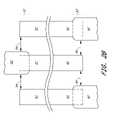
- FIGS. 1A-1Fare one methods proposed for extending the capabilities of photolithographic techniques beyond their minimum pitch. Such a method is illustrated in FIGS. 1A-1F and described in U.S. Pat. No. 5,328,810, issued to Lowrey et al., the entire disclosure of which is incorporated herein by reference.
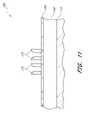
- photolithographyis first used to form a pattern of lines 10 in a photoresist layer overlying a layer 20 of an expendable material and a substrate 30 .
- the patternis then transferred by an etch step (preferably anisotropic) to the layer 20 , forming placeholders, or mandrels, 40 .
- an etch steppreferably anisotropic
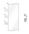
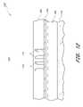
- the photoresist lines 10can be stripped and the mandrels 40 can be isotropically etched to increase the distance between neighboring mandrels 40 , as shown in FIG. 1C .
- a layer 50 of materialis subsequently deposited over the mandrels 40 , as shown in FIG. 1D .
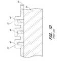
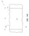
- Spacers 60i.e., material extending or originally formed extending from sidewalls of another material, are then formed on the sides of the mandrels 40 by preferentially etching the spacer material from horizontal surfaces in a directional spacer etch, as shown in FIG. 1E .
- the remaining mandrels 40are then removed, leaving behind the freestanding spacers 60 , which together act as an etch mask for patterning underlying layers, as shown in FIG. 1F .
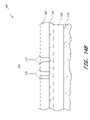
- the same widthnow includes two features and two spaces defined by the spacers 60 .
- the smallest feature size possible with a photolithographic techniqueis effectively decreased.
- pitch doublingthis reduction in pitch is conventionally referred to as pitch “doubling,” or, more generally, pitch “multiplication.” That is, conventionally “multiplication” of pitch by a certain factor actually involves reducing the pitch by that factor.
- pitch “doubling”this reduction in pitch is conventionally referred to as pitch “doubling,” or, more generally, pitch “multiplication.” That is, conventionally “multiplication” of pitch by a certain factor actually involves reducing the pitch by that factor.
- pitch “doubling”pitch “multiplication” of pitch by a certain factor actually involves reducing the pitch by that factor.
- the critical dimension of a mask scheme or circuit designis the scheme's minimum feature dimension. Due to factors such as geometric complexity and different requirements for critical dimensions in different parts of an integrated circuit, typically not all features of the integrated circuit will be pitch multiplied. Consequently, pitch multiplied features will often need to be connected to or otherwise aligned with respect to non-pitch multiplied features in some part of the integrated circuit. Because these non-pitch multiplied features generally have larger critical dimensions than the pitch multiplied features, the margin of error for aligning the non-pitch multiplied features to contact the pitch multiplied features can be small. Moreover, because the critical dimensions of pitch-multiplied lines may be near the resolution and/or overlay limits of many photolithographic techniques, shorting neighboring pitch multiplied features is an ever-present possibility. Such shorts can undesirably cause the integrated circuit to malfunction.
- a methodfor forming an integrated circuit.
- the methodcomprises providing a substrate with an overlying temporary layer and a photodefinable layer overlying the temporary layer.
- a patternis formed in the photodefinable layer and transferred to the temporary layer to form a plurality of placeholders in the temporary layer.
- a blanket layer of spacer materialis then deposited over the plurality of placeholders.
- the spacer materialis selectively removed from horizontal surfaces.
- the placeholdersare selectively removed relative to the spacer material to form a plurality of spacer loops.
- the spacer loopsare etched to form a pattern of separated spacers.
- An other photodefinable layeris formed around and on the same level as the separated spacers.
- Interconnectsare patterned in the other photodefinable layer.
- the interconnectsare wider than the spacers and contact the spacers and are aligned with one long side of the interconnects inset from or collinear with a corresponding long side of the spacers.
- a methodfor semiconductor fabrication.
- the methodcomprises providing a substrate and forming an elongated spacer over the substrate by pitch multiplication.
- a photoresist lineis then formed.
- the photoresist lineis in contact with an end of the spacer in a contact region.
- the spacerforms a boundary for only two faces of the photoresist line in the contact region.
- a processfor fabricating an integrated circuit.
- the processcomprises forming a first plurality of mask lines and forming a photodefinable layer around the mask lines.
- the photodefinable layerhas a thickness less than a height of the mask lines.
- a plurality of featuresis patterned in the photodefinable layer.
- a partially fabricated integrated circuitcomprises a substrate and a first plurality of mask lines overlying the substrate.
- a photodefinable layercontacts the mask lines.
- the photodefinable layerhas a thickness less than a height of the mask lines.
- an integrated circuitcomprises a plurality of interconnects, each having a first portion with a first width in an array region and a second portion with a second width in a periphery region.
- the second widthis larger than the first width.
- An end of each of the second interconnect portionscontacts an end of each of the first interconnect portions.
- One side of each of the second interconnect portions, extending along a length of one of the second interconnect portions,is substantially collinear with or inset from one side of each of the first interconnect portions, extending along a length of one of the first interconnect portions.
- an integrated circuitcomprises a plurality of interconnects each having a first portion and a second portion.
- the first portion of the interconnectsare substantially parallel to each other between first and second spaced planes extending perpendicular to the lines.
- the first portion and the second portioncontact in an overlap region. Only one corner of the second portion protrudes beyond a side of the first portion in the overlap region.
- FIGS. 1A-1Fare schematic, cross-sectional side views of mask lines, formed in accordance with a prior art pitch multiplication method
- FIGS. 2A and 2Bare schematic, top plan views of conductive lines in an integrated circuit
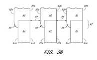
- FIGS. 3A-3Dare schematic, top plan views of a partially formed integrated circuit, in accordance with preferred embodiments of the invention.
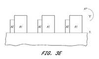
- FIG. 3Eis a schematic, cross-sectional side view the partially formed integrated circuit of FIGS. 3A , 3 B, 3 C or 3 D, in accordance with preferred embodiments of the invention.
- FIGS. 4A-4Bare schematic, top plan and cross-sectional side views, respectively, of a partially formed integrated circuit, in accordance with preferred embodiments of the invention.
- FIG. 5is a schematic, cross-sectional side view of the partially formed memory device of FIGS. 4A-4B after forming lines in a selectively definable layer, in accordance with preferred embodiments of the invention
- FIG. 6is a schematic, cross-sectional side view of the partially formed integrated circuit of FIG. 5 after widening spaces between photoresist lines, in accordance with preferred embodiments of the invention.
- FIG. 7is a schematic, cross-sectional side view of the partially formed integrated circuit of FIG. 6 after etching through a hard mask layer, in accordance with preferred embodiments of the invention.
- FIG. 8is a schematic, cross-sectional side view of the partially formed integrated circuit of FIG. 7 after transferring a pattern from the photoresist and hard mask layers to a temporary layer, in accordance with preferred embodiments of the invention
- FIG. 9is a schematic, cross-sectional side view of the partially formed integrated circuit of FIG. 8 after depositing a blanket layer of a spacer material, in accordance with preferred embodiments of the invention.
- FIG. 10is a schematic, cross-sectional side view of the partially formed integrated circuit of FIG. 9 after a spacer etch, in accordance with preferred embodiments of the invention.
- FIG. 11is a schematic, cross-sectional side view of the partially formed integrated circuit of FIG. 10 after removing remnants of the temporary layer from between spacers, in accordance with preferred embodiments of the invention.
- FIG. 12is a schematic, cross-sectional side view of the partially formed integrated circuit of FIG. 11 after depositing a protective layer, in accordance with preferred embodiments of the invention.
- FIG. 13is a schematic, top plan view of the partially formed integrated circuit of FIG. 12 after patterning the protective layer, in accordance with preferred embodiments of the invention.
- FIGS. 14A-14Bare schematic, top plan and cross-sectional side views of the partially formed integrated circuit of FIG. 13 after etching exposed portions of spacers, in accordance with preferred embodiments of the invention.
- FIGS. 15A-15Bare schematic, top plan and cross-sectional side views of the partially formed integrated circuit of FIG. 13 after removing the protective layer, in accordance with preferred embodiments of the invention.
- FIG. 16is a schematic, cross-sectional side view of the partially formed integrated circuit of FIGS. 15A-15B after depositing a photodefinable layer, in accordance with preferred embodiments of the invention.
- FIGS. 17A-17Bare schematic, top plan and cross-sectional side views of the partially formed integrated circuit of FIG. 16 after patterning the photodefinable layer, in accordance with preferred embodiments of the invention.
- FIG. 18is a schematic, top plan view of the partially formed integrated circuit of FIGS. 17A-17B showing overdevelopment of the photodefinable layer, in accordance with some preferred embodiments of the invention.
- FIG. 19is a schematic, cross-sectional side view of the partially formed integrated circuit of FIGS. 17A-17B after etching through a hard mask layer, in accordance with preferred embodiments of the invention.
- FIG. 20is a schematic, cross-sectional side view of the partially formed integrated circuit of FIG. 18 after etching the additional masking layer, in accordance with preferred embodiments of the invention.
- FIG. 21is a schematic, top plan view of the partially formed integrated circuit of FIG. 20 after forming conductive interconnects in the substrate, in accordance with preferred embodiments of the invention.
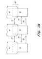
- FIGS. 2A and 2Bshows such an idealized alignment of pitch multiplied lines 91 and non-pitch multiplied lines 92 .
- FIG. 2Ashows an arrangement in which every line 91 is contacted on the same side with a line 92 and
- FIG. 2Bshows an arrangement in which lines 92 contact the lines 91 on alternating sides.
- misalignmentscan occur in the overlap region 93 in which the lines 91 and 92 contact, however.
- the lines 92may all be misaligned in one direction. Because the lines 92 are wider than the space separating the lines 91 , a single line 92 can short two lines 91 if the misalignment is severe.
- Another form of misalignmentcan occur when a line 92 is skewed in one direction, relative to other lines 92 . This can also cause a short if neighboring lines 92 contact. In reality, all these forms of misaligmuents can occur concurrently.
- the tolerances for misalignments of the lines 92 and 91are preferably large.
- the distances 94 between each line 92 and each line 91 and the distances 95 between neighboring lines 92are preferably each maximized to maximize tolerances. More preferably, both of the distances 94 and 95 are maximized.
- a first featuresuch as a line 91
- a second featuresuch as a line 92
- the second featureis aligned so that only one of its sides 92 a extends beyond a corresponding side 91 a of the first feature, as illustrated in FIG. 3A .
- the other side 92 bis shown inset from the corresponding side 91 b of the first feature.
- the corners 96can protrude beyond either side 91 a or 91 b or some corners 96 can protrude beyond the side 91 a and others beyond the side 91 b , since concerns of two neighboring corners 96 shorting are minimized by the alternating arrangement.
- the protruding corner 96can be formed rounded.
- the distance, e.g., distance 94 , between neighboring features, e.g., the lines 91 and 92 , in the overlap region, e.g., region 93can be increased relative to lines 92 without rounding.
- the second featureis preferably formed in photoresist by photolithography.
- the photoresistis preferably formed below the vertical height of the first feature, as illustrated in FIG. 3E for lines 91 and 92 , the lines 91 having a height 97 .
- the first features, such as the lines 91act as walls that permit the second features, such as the lines 92 , to grow, if at all, in only one direction.
- misalignment tolerancescan be increased.
- any misalignmentscan be weighted in one direction, e.g., in the direction of the sides 91 b , while still maintaining an adequate distance 94 between lines 92 and 91 .
- the photoresistcan be overdeveloped to narrow the second features to further minimize the possibility of shorting.
- the overdevelopmentcan include any process which reduces the critical dimension of the lines 92 .
- the overdevelopmentcan include extending the development period and/or performing an additional treatment or technique to controllably remove resist, e.g., partially exposed resist.
- the overdevelopmentcan remove resist in the exposure threshold or “gray” area between the area fully exposed to radiation transmitted through the reticle and lens system and the area that is “dark” or exposed to a light intensisty below the exposure threshold for the resist.
- the first mask featuressuch as the lines 91
- the second mask featuressuch as the lines 92
- the second featuresare preferably patterned in photoresist that overlaps the first features.
- the photoresistis typically patterned by being exposed to radiation through a reticle and then developed.
- radiatione.g., light
- the radiationactivates a photosensitive compound, e.g., a photo-induced acid generator (PAG), which decreases the solubility of the photoresist, e.g., by causing it to polymerize.
- a photosensitive compounde.g., a photo-induced acid generator (PAG)
- PAGphoto-induced acid generator
- Such photoactivated chemicalscan diffuse, thereby causing the lines 92 to expand to areas that are not irradiated. In addition to decreasing the precision with which the lines 92 are formed, this diffusion can also cause the lines 92 to expand, thereby decreasing alignment tolerances by decreasing distances 94 between the lines 91 and 92 .
- the photoresistis preferably formed at a level below the top of the first mask features, such as the lines 91 .
- the photoresistis then patterned to form the second features.
- the first mask featuresact as a wall, only allowing diffusion of photogenerated acid from PAG's in a direction away from those first mask features.
- the misalignment tolerance in the region 93can be increased by an amount approximately equal to the amount that the photogenerated acids would have otherwise diffused to expand the lines 92 . Since diffusion can only occur in one direction, the risk of shorting from diffusion is effectively halved in the overlap region.
- negative photoresistis utilized in particularly advantageous embodiments.
- the rounding effectcan be increased. It will be appreciated that light reaching the photoresist between lines 91 is attenuated due to a shadowing affect caused by the presence of the taller lines 91 . Moreover, this attenuation will increase with increasing distance down the lines 91 away from the ends of the lines 91 .
- the attenuationfurther rounds off and narrows the width of the lines 92 between lines 91 .
- the distances between the wider lines 92 and the neighboring narrower lines 91can be further increased, thereby further increasing misalignment margins.
- a combination of positive and negative photoresistis used, with the positive photoresist used in forming (preferably via a process utilizing spacers) the lines 91 and the negative photoresist using in forming the lines 92 .
- the negative photoresistadvantageously increases the rounding discussed above, while the positive photoresist advantageously allows a higher resolution relative to the negative photoresist.
- FIG. 4Ashows a top view of an integrated circuit 100 , which is preferably a memory chip.
- a central region 102the “array,” is surrounded by a peripheral region 104 , the “periphery.”
- the array 102will typically be densely populated with conducting lines and electrical devices such as transistors and capacitors.
- the electrical devicesform a plurality of memory cells, which are typically arranged in a regular pattern, such as rows.
- pitch multiplicationcan be used to form features such as rows/columns of transistors, capacitors or interconnects in the array 102 , as discussed below.
- the periphery 104typically comprises features larger than those in the array 102 .
- Conventional photolithography, rather than pitch multiplication,is preferably used to pattern features, such as logic circuitry, in the periphery 104 , because the geometric complexity of logic circuits located in the periphery 104 makes using pitch multiplication difficult, whereas the regular grid typical of memory array patterns is conducive to pitch multiplication.
- some devices in the peripheryrequire larger geometries due to electrical constraints, thereby making pitch multiplication less advantageous than conventional photolithography for such devices. It will be appreciated that the periphery 104 and the array 102 are not draw to scale and their relative positions may vary from that depicted.
- a partially formed integrated circuit 100is provided.
- a substrate 110is provided below various masking layers 120 - 160 .
- the layers 120 - 160will be etched to form a mask for patterning the substrate 110 to form various features, as discussed below.
- the materials for the layers 120 - 160 overlying the substrate 110are preferably chosen based upon consideration of the chemistry and process conditions for the various pattern forming and pattern transferring steps discussed herein. Because the layers between a topmost selectively definable layer 120 , which preferably is definable by a lithographic process, and the substrate 110 will preferably function to transfer a pattern derived from the selectively definable layer 120 to the substrate 110 , the layers between the selectively definable layer 120 and the substrate 110 are preferably chosen so that they can be selectively etched relative to other exposed materials. It will be appreciated that a material is considered selectively, or preferentially, etched when the etch rate for that material is at least about 5 times greater, preferably about 10 times greater and, most preferably, at least about 40 times greater than that for surrounding materials.
- the selectively definable layer 120overlies a first hard mask, or etch stop, layer 130 , which overlies a temporary layer 140 , which overlies a second hard mask, or etch stop, layer 150 , which overlies an additional mask layer 160 , which overlies the substrate 110 to be processed (e.g., etched) through a mask.
- the mask through which the substrate 110 is processedis formed in the second hard mask layer 150 or in the additional mask layer 160 .
- both the mask and the underlying substrateare exposed to an etchant, which preferentially etches away the substrate material.
- the etchantsalso wear away the mask materials, albeit at a slower rate.
- the maskcan be worn away by the etchant before the pattern transfer is complete.
- the additional mask layer 160which preferably comprises a thick layer of amorphous carbon, is desirable to prevent the mask pattern from being worn away before the pattern transfer is complete.
- the illustrated embodimentshows the use of the additional mask layer 160 .
- the additional mask layer 160can be omitted in embodiments where the substrate 110 is relatively simple, e.g., where the substrate 110 is a single layer of material and where the depth of the etch is moderate.
- the second hard mask layer 150may be a sufficient mask for transferring a pattern to the substrate 110 .
- the various other layers, such the second hard mask layer 150 itselfmay be omitted and overlying mask layers may be sufficient for the desired pattern transfer.
- the illustrated sequence of layersis particularly advantageous for transferring patterns to difficult to etch substrates, such as a substrate 110 comprising multiple materials or multiple layers of materials, or for forming small and high aspect ratio features.
- the selectively definable layer 120is preferably formed of a photoresist, including any photoresist known in the art.
- the photoresistcan be any photoresist compatible with 13.7 nm, 157 nm, 193 nm, 248 nm or 365 nm wavelength systems, 193 nm wavelength immersion systems or electron beam lithographic systems.
- preferred photoresist materialsinclude argon fluoride (ArF) sensitive photoresist, i.e., photoresist suitable for use with an ArF light source, and krypton fluoride (KrF) sensitive photoresist, i.e., photoresist suitable for use with a KrF light source.
- ArFargon fluoride
- KrFkrypton fluoride
- ArF photoresistsare preferably used with photolithography systems utilizing relatively short wavelength light, e.g., 193 nm.
- KrF photoresistsare preferably used with longer wavelength photolithography systems, such as 248 nm systems.
- the layer 120 and any subsequent resist layerscan be formed of a resist that can be patterned by nano-imprint lithography, e.g., by using a mold or mechanical force to pattern the resist.
- the material for the first hard mask layer 130preferably comprises an inorganic material, and exemplary materials include silicon oxide (SiO 2 ), silicon or a dielectric anti-reflective coating (DARC), such as a silicon-rich silicon oxynitride.
- the first hard mask layer 130is a dielectric anti-reflective coating (DARC).
- the temporary layer 140is preferably formed of amorphous carbon, which offers very high etch selectivity relative to the preferred hard mask materials. More preferably, the amorphous carbon is a form of transparent carbon that is highly transparent to light and which offers further improvements for photo alignment by being transparent to wavelengths of light used for such alignment. Deposition techniques for forming a highly transparent carbon can be found in A. Helmbold, D. Meissner, Thin Solid Films, 283 (1996) 196-203, the entire disclosure of which is incorporated herein by reference.
- DARCsfor the first hard mask layer 130 can be particularly advantageous for forming patterns having pitches near the resolution limits of a photolithographic technique.
- the DARCscan enhance resolution by minimizing light reflections, thus increasing the precision with which photolithography can define the edges of a pattern.
- a bottom anti-reflective coating(BARC) (not shown) can similarly be used in addition to the first hard mask layer 130 to control light reflections.
- the second hard mask layer 150preferably comprises a dielectric anti-reflective coating (DARC) (e.g., a silicon oxynitride), silicon or aluminum oxide (Al 2 O 3 ).
- DARCdielectric anti-reflective coating
- BARCbottom anti-reflective coating
- the additional mask layer 160is preferably formed of amorphous carbon due to its excellent etch selectivity relative to many materials.
- the thicknesses of the layers 120 - 160are preferably chosen depending upon compatibility with the etch chemistries and process conditions described herein. For example, when transferring a pattern from an overlying layer to an underlying layer by selectively etching the underlying layer, materials from both layers are removed to some degree.
- the upper layeris preferably thick enough so that it is not worn away over the course of the pattern transfer.
- the selectively definable layer 120is a photodefinable layer preferably between about 50-300 nm thick and, more preferably, between about 200-250 nm thick.
- the first hard mask layer 130is preferably between about 100-400 nm thick and, more preferably, between about 150-300 nm thick.
- the temporary layer 140is preferably between about 100-200 nm thick and, more preferably, between about 120-150 nm thick.
- the second hard mask layer 150is preferably between about 20-80 nm thick and, more preferably, about 50 nm thick and the additional mask layer 160 is preferably between about 200-500 nm thick and, more preferably, about 300 nm thick.
- various layers discussed hereincan be formed by various methods known to those of skill in the art.
- various vapor deposition processessuch as chemical vapor deposition
- a low temperature chemical vapor deposition processis used to deposit the hard mask layers or any other materials, e.g., spacer material, over the mask layer 160 , where the mask layer 160 is formed of amorphous silicon.
- Such low temperature deposition processesadvantageously prevent chemical or physical disruption of the amorphous carbon layer.
- Spin-on-coating processescan be used to form photodefinable layers.
- amorphous carbon layerscan be formed by chemical vapor deposition using a hydrocarbon compound, or mixtures of such compounds, as carbon precursors.
- Exemplary precursorsinclude propylene, propyne, propane, butane, butylene, butadiene and acetelyne.
- a suitable method for forming amorphous carbon layersis described in U.S. Pat. No. 6,573,030 B1, issued to Fairbairn et al. on Jun. 3, 2003, the entire disclosure of which is incorporated herein by reference.
- the amorphous carbonmay be doped.
- a suitable method for forming doped amorphous carbonis described in U.S. patent application Ser. No. 10/652,174 to Yin et al., the entire disclosure of which is incorporated herein by reference.
- a pattern of spacersis formed by pitch multiplication.
- a pattern comprising spaces or trenches 122 delimited by photodefinable material features 124is formed in the photodefinable layer 120 .
- the trenches 122can be formed by, e.g., photolithography, in which the layer 120 is exposed to radiation through a reticle and then developed. After being developed, the remaining photodefinable material, photoresist in the illustrated embodiment, forms mask features such as the illustrated lines 124 (shown in cross-section only).
- the pitch of the resulting lines 124is equal to the sum of the width of a line 124 and the width of a neighboring space 122 .
- the pitchis preferably at or near the limits of the photolithographic technique used to pattern the photodefinable layer 120 .
- the pitch of the lines 124can be about 100 nm.
- the pitchmay be at the minimum pitch of the photolithographic technique and the spacer pattern discussed below can advantageously have a pitch below the minimum pitch of the photolithographic technique.
- the spaces 122can optionally be widened or narrowed to a desired dimension.
- the spacers 122can be widened by etching the photoresist lines 124 , to form modified spaces 122 a and lines 124 a .
- the photoresist lines 124are preferably etched using an isotropic etch, such as a sulfur oxide plasma, e.g., a plasma comprising SO 2 , O 2 , N 2 and Ar.
- the extent of the etchis preferably selected so that the widths' of the lines 124 a are substantially equal to the desired spacing between the later-formed spacers 175 , as will be appreciated from the discussion of FIGS. 9-11 below.
- this etchallows the lines 124 a to be narrower than would otherwise be possible using the photolithographic technique used to pattern the photodefinable layer 120 .
- the etchcan smooth the edges of the lines 124 a , thus improving the uniformity of those lines.
- the spaces between the spaces 122can be narrowed by expanding the lines 124 to a desired size. For example, additional material can be deposited over the lines 124 or the lines 124 can be chemically reacted to form a material having a larger volume to increase their size.
- the pattern in the (modified) photodefinable layer 120is preferably transferred to the temporary layer 140 to allow for deposition of a layer 170 of spacer material ( FIG. 9 ).
- the temporary layer 140is preferably formed of a material that can withstand the process conditions for spacer material deposition and etch, discussed below. In other embodiments where the deposition of spacer material is compatible with the photodefinable layer 120 , the temporary layer 140 can be omitted and the spacer material can be deposited directly on the photo-defined features 124 or the modified photodefined features 124 a of the photodefinable layer 120 itself.
- the material forming the temporary layer 140is preferably selected such that it can be selectively removed relative to the material for the spacers 175 ( FIG. 10 ) and the underlying etch stop layer 150 .
- the layer 140is preferably formed of amorphous carbon.
- the pattern in the photodefinable layer 120is preferably first transferred to the hard mask layer 130 , as shown in FIG. 7 .
- This transferis preferably accomplished using an anisotropic etch, such as an etch using a fluorocarbon plasma, although a wet (isotropic) etch may also be suitable if the hard mask layer 130 is thin.
- Preferred fluorocarbon plasma etch chemistriesinclude CF 4 , CFH 3 , CF 2 H 2 and CF 3 H.
- the pattern in the photodefinable layer 120is then transferred to the temporary layer 140 , as shown in FIG. 8 , preferably using a SO 2 -containing plasma, e.g., a plasma containing SO 2 , O 2 and Ar.
- a SO 2 -containing plasmae.g., a plasma containing SO 2 , O 2 and Ar.
- the SO 2 -containing plasmacan etch carbon of the preferred temporary layer 140 at a rate greater than 20 times and, more preferably, greater than 40 times the rate that the hard mask layer 130 is etched.
- a suitable SO 2 -containing plasmais described in U.S. patent application Ser. No. 10/931,772 to Abatchev et al., filed Aug. 31, 2004, entitled Critical Dimension Control, the entire disclosure of which is incorporate herein by reference.
- the SO 2 -containing plasmacan simultaneously etch the temporary layer 140 and also remove the photodefinable layer 120 .
- the resulting lines 124 bconstitute the placeholders or mandrels along which a pattern of spacers 175 ( FIG. 10 ) will be formed.
- a layer 170 of spacer materialis preferably blanket deposited conformally over exposed surfaces, including the hard mask layer 130 , the hard mask 150 and the sidewalls of the temporary layer 140 .
- the hard mask layer 130can be removed before depositing the layer 170 .
- the spacer materialcan be any material that can act as a mask for transferring a pattern to the underlying substrate 110 , or that otherwise can allow processing of underlying structures through the mask being formed.
- the spacer materialpreferably: 1) can be deposited with good step coverage; 2) can be deposited at a temperature compatible with the temporary layer 140 ; 3) can be selectively etched relative to the temporary layer 140 and any layer underlying the temporary layer 140 .
- Preferred materialsinclude silicon oxides and nitrides.
- the spacer materialis preferably deposited by chemical vapor deposition or atomic layer deposition.
- the layer 170is preferably deposited to a thickness of between about 20-60 nm and, more preferably, about 20-50 nm.
- the step coverageis about 80% or greater and, more preferably, about 90% or greater.
- the spacer layer 170is then subjected to an anisotropic etch to remove spacer material from horizontal surfaces 180 of the partially formed integrated circuit 100 .
- an etchalso known as a spacer etch, can be performed using HBr/Cl plasma.
- the etchincludes a physical component and preferably can also include a chemical component and can be, e.g., a reactive ion etch (RIE), such as a Cl 2 , HBr etch.
- RIEreactive ion etch
- Such an etchcan be performed, for example, using a LAM TCP9400 flowing about 0-50 sccm Cl 2 and about 0-200 sccm HBr at about 7-60 mTorr pressure with about 300-1000 W top power and about 50-250 W bottom power.
- the hard mask layer 130 (if still present) and the temporary layer 140are next removed to leave freestanding spacers 175 .
- the temporary layer 140is selectively removed, preferably using a sulfur-containing plasma etch such as an etch using SO 2 .
- the pitch of the spacers 175is roughly half that of the photoresist lines 124 and spaces 122 ( FIG. 5 ) originally formed by photolithography.
- spacers 175 having a pitch of about 100 nm or lesscan be formed. It will be appreciated that because the spacers 175 are formed on the sidewalls of the features or lines 124 b , the spacers 175 generally follow the outline of the pattern of features or lines 124 a in the photodefinable layer 120 and, so, typically form a closed loop.
- the loops formed by the spacers 175are separated into individual lines. This separation is preferably accomplished by an etch that for each loop forms two separate lines of spacers 175 corresponding to two separate conductive paths in the substrate 110 . It will be appreciated that more than two lines can be formed, if desired, by etching the spacers 175 at more than two locations.
- a protective maskis preferably formed over parts of the lines to be retained and the exposed, unprotected parts of the spacer loops are then etched. The protective mask is then removed to leave a plurality of electrically separated lines.
- a protective material forming a second protective layer 300is preferably deposited around and over the spacers 175 and the parts of the layers 150 and 160 .
- the protective materialis preferably a photodefinable material such as photoresist.
- an anti-reflective coating(not shown) can be provided under the layer 300 , e.g., directly above the substrate 110 , to improve photolithography results.
- the photoresist and the anti-reflective coatingcan be deposited using various methods known in the art, including spin-on-coating processes.
- a protective mask 310is subsequently patterned in the second protective layer 300 , e.g., by photolithography, to protect desired parts of the underlying spacers 175 from a subsequent etch.
- portions of the loopsare exposed for etching in at least two separate locations.
- the exposed portions of the loopsare preferably the ends of the loops formed by the spacers 175 , as illustrated.
- the protective layer 300can be formed of any material that can be selectively removed, e.g., relative to the spacers 175 , the layers 150 - 160 and the substrate 110 .
- the protective mask 310can be formed in another material, e.g., photoresist, overlying the layer 300 .
- FIG. 14Ashows a side view of the resulting structure, taken along the vertical plane 14 B of FIG. 14A .
- the protective materialis preferably selectively removed.
- the partially formed integrated circuit 100can be subjected to an ash process to remove the protective material.
- the spacers 175are not attacked during this removal step and that the layer 160 is protected by the second hard mask layer 150 .
- a plurality of individual mask lines 320are formed.
- FIG. 15Ashows a top plan view of the resultant structure and
- FIG. 15Bshows a cross-sectional side view taken along the vertical plane 15 B of FIG. 15A .
- a second patternis stitched or overlapped with the pattern of spacers 320 .
- the second patternis overlaid on the spacers 320 to pattern features that will contact the features defined by the spacers 320 .
- a photodefinable layer 400is preferably formed around the spacers 320 , as shown in FIG. 16 .
- the photodefinable layer 400preferably has a height below the level of the spacers 320 .
- the photodefinable layer 400is formed of photoresist and, more preferably, negative photoresist.
- the photoresistcan be deposited to the desired height using a scan coating method, such as that commercially available from Tokyo Electron Limited (TEL) of Tokyo, Japan.
- a relatively thick layer of photoresistcan be deposited and then etched back to the desired height.
- the etch backdoes not activate PAG's or otherwise detrimentally effect the photoresist for subsequent exposure and development steps.
- the photodefinable layer 400is preferably about 80% or less and, more preferably, about 75-50% of the height of the spacers 320 .
- a pattern corresponding to line extensions or contacts to features to be defined by the spacers 320is next formed in the photodefinable layer 400 .
- the photodefinable layer 400can be patterned using any photolithographic technique, including the same photolithographic technique used to pattern the photodefinable layer 120 .
- the photodefinable layer 400is patterned using a higher resolution technique than the photodefinable layer 120 .
- the photodefinable layer 400can be patterned using 193 nm photolithography to form features having a pitch of about 140 nm.
- the photodefinable layer 400is patterned using a lithographic technique that allows patterning with a pitch less than that of the spacers 320 .
- lithographic techniquethat allows patterning with a pitch less than that of the spacers 320 .
- electron beam lithographywhich has high resolution but relatively poor alignment capabilities, can be used to pattern the photodefinable layer 400 .
- a pattern of features 410is formed in the photodefinable layer 400 .
- the features 410can be used to pattern features of different sizes than the spacers 320 , including landing pads, local interconnects, etc.
- the features 410preferably overlap the pattern of spacers 320 to ultimately form interconnects that contact interconnects formed using the spacers 320 .
- the features 410function as interconnect masking structures.
- the interconnects formed using the features 410have a larger critical dimension than those formed using the spacers 320 .
- FIG. 17Ashows a top plan view of the resulting structure, with elongated photodefined features 410 and spacers 320 .
- the spacers 320each have two opposing sides, one labeled 320 a and the other unlabeled, that extend the length of the spacers 320 .
- the shape of the features 410correspond to the location of light reaching the photoresist layer 400 ( FIG. 16 ), where the photoresist layer 400 comprises negative photoresist.
- the photoresist layer 400comprises positive photoresist
- lightis directed to all areas of the partially fabricated integrated circuit 100 , except for the location of the features 410 .
- the shape of the features 410 in the reticlecan be rectangular, with sharp corners, while still advantageously forming rounded corners. More preferably, the reticle is shaped to ensure rounding of the corners, especially where positive photoresist is used.
- the reticlecan be positioned so that the features 410 align with one of their long sides 410 a inset from the corresponding long sides 320 a of the spacers 320 to ensure that the sides 410 a do not extend beyond the sides 320 a .
- the sides 410 amay be further inset from the sides 320 a or may be collinear with the sides 320 a .
- a targeted or desired position of the sides 410 ais collinear with or slightly inset from the sides 320 a .
- the photodefined features 410contact only one side of each of the spacers 320 .
- the photodefined features 410contact the unlabeled sides of the spacers 320 , but not the sides 320 a.
- FIG. 17Bshows a cross-sectional side view of the partially fabricated integrated circuit 100 , taken along the vertical plane 17 B of FIG. 17A .
- the features 410may be larger than desired (solid line) or may be positioned beyond the sides 410 a .
- the photoresist layer 400can be overdeveloped to further narrow those features to a desired size (dotted line) and/or position.
- the pattern of features 410 and spacers 320can next be transferred to the additional mask layer 160 .
- the additional mask layer 160comprises a material having good etch selectivity to the material(s) of the substrate 110 , and vice versa, to allow for an effective transfer and later mask removal.
- the hard mask layer 150 overlying the additional mask layer 160is first etched ( FIG. 19 ).
- the hard mask layer 150is preferably anisotropically etched, preferably using a fluorocarbon plasma. Alternatively, an isotropic etch may be used if the hard mask layer 150 is relatively thin. While not shown, it will be understood that in the array region 102 , the hard mask 150 remains only directly under the spacers 320 .
- the additional mask layer 160is then anisotropically etched, preferably using a SO 2 -containing plasma, which can simultaneously remove the features 410 .
- FIG. 20shows a schematic side view of the resulting partially formed integrated circuit 100 in the region of overlap between the two patterns.
- the pattern in the additional mask layer 160can then be transferred to the substrate 110 .
- the pattern transfercan be readily accomplished using conventional etches appropriate for the material or materials of the substrate 110 .
- the substrate 110comprises a conductor suitable for acting as electrical interconnects between electrical devices.
- the substratecomprises doped silicon or a metal layer, such as an aluminum or copper layer.
- the mask lines 320 and 410can directly correspond to the desired placement of interconnects in the substrate 110 .
- FIG. 21shows a resulting structure, with interconnects 420 formed in the partially formed integrated circuit 100 .
- the substratecan be an insulator and the location of mask features can correspond to the desired location of insulators in an integrated circuit.
- the spacers 320block photogenerated chemicals, such as acid from PAG's, from diffusing in one direction, the features 410 are prevented from growing in that direction in the region of contact with the spacers 320 .
- the misalignment toleranceespecially in the direction in which diffusion is blocked, may be thought of as increasing by the amount that the features 410 would have otherwise expanded.
- the rounding of the cornersdue partially to shadowing from the taller spacers extending above the second resist layer, also increases the misalignment tolerance by increasing the distance between the spacers 320 and the features 410 .
- any misalignmentcan be weighted in that direction, since further expansion in that direction is minimized, especially where the photoresist is overdeveloped.
- the features 410preferably contact the spacers 320 both at butting ends and from the side, a relatively high contact area can be achieved.
- the spacers 320form a boundary for exactly two faces of the features 410 , e.g., line end faces and on one side of the features 320 .
- a high contact areacan advantageously be maintained even after trimming by overdevelopment. For example, if the features 410 were centered on the spacers 320 , trimming may leave the features 410 only contacting the spacers 320 ends. The off-set positioning above, however, allows the features 410 to contact the spacers 320 both at butting ends and from the side, thereby increasing the contact area between those two parts.
- transferring a pattern from a first level to a second levelinvolves forming features in the second level that generally correspond to features on the first level.
- the path of lines in the second levelwill generally follow the path of lines on the first level and the location of other features on the second level will correspond to the location of similar features on the first level.
- the precise shapes and sizes of featurescan vary from the first level to the second level, however.
- the sizes of and relative spacings between the features forming the transferred patterncan be enlarged or diminished relative to the pattern on the first level, while still resembling the same initial “pattern.”
- the transferred patternis still considered to be the same pattern as the initial pattern.
- forming spacers around mask featurescan change the pattern.
- the pitch of the spacers 320can be more than doubled.
- further pitch multiplicationcan be accomplished by forming additional spacers around the spacers 320 , then removing the spacers 320 , then forming spacers around the spacers that were formerly around the spacers the 175, and so on.
- An exemplary method for further pitch multiplicationis discussed in U.S. Pat. No. 5,328,810 to Lowrey et al.
- the spacers 320 or the features 410can each be spaced at varying distances to each other. Moreover, while all are illustrated contacting the spacers 320 from the same side, some of the features 410 can be positioned on different, e.g., sides. Moreover, while illustrated parallel over their entire lengths for illustrate, the distance between the spacers 320 can vary over some or all of their lengths. Preferably, however, the spacers 320 , and resulting interconnects 420 , are parallel over some distance, e.g., between first and second planes 500 and 502 extending perpendicular to the spacers 320 ( FIGS. 18 and 21 ).
- the illustrated spacers 320are preferably parallel in the array region 102 of a DRAM to connect the tightly packed memory cells in that array region.
- various parts of the spacers 320can be formed at angles relative to other parts of the spacers 320 .
- parts of the features 410can be formed at angles relative to the spacers 320 or to other parts of the features 410 .
- the features 410can diverge away from the points of contact with the spacers 320 to allow for increased separation between those features.
- more than two patternscan be consolidated on a mask layer before transferring the consolidated pattern to the substrate.
- additional mask layerscan be deposited above the layer 150 .
- patterns corresponding to landing pads and additional interconnectscan be transferred to a supplemental mask layer (not shown) overlying the hard mask layer 150 and then an overlying photodefinable layer (not shown) can be patterned and the pattern transferred to underlying layers.
- the substrate 110can then be processed through the resulting mask pattern.
- processing through the various mask layerscan involve subjecting layers underlying the mask layers to any semiconductor fabrication process.
- processingcan involve ion implantation, diffusion doping, depositing, or wet etching, etc. through the mask layers and onto underlying layers.
- the mask layerscan be used as a stop or barrier for chemical mechanical polishing (CMP) or CMP can be performed on the mask layers to allow for both planarizing of the mask layers and etching of the underlying layers.
- CMPchemical mechanical polishing
- features formed by pitch multiplication or employing spacers on soft or hard masksare “stitched” or aligned with features formed by a masking technique with a lower resolution.
- pitch multiplied mask featuresare made to contact features formed by conventional photolithography.
- the pitch multiplied featurespreferably have a pitch below the minimum pitch of the photolithographic technique used for patterning the other features.
- the preferred embodimentscan be used to form any integrated circuit, they are particularly advantageously applied to form devices having arrays of electrical devices, including logic or gate arrays and volatile and non-volatile memory devices such as DRAM, ROM or flash memory.
Landscapes
- Engineering & Computer Science (AREA)
- Manufacturing & Machinery (AREA)
- Physics & Mathematics (AREA)
- Condensed Matter Physics & Semiconductors (AREA)
- General Physics & Mathematics (AREA)
- Computer Hardware Design (AREA)
- Microelectronics & Electronic Packaging (AREA)
- Power Engineering (AREA)
- Inorganic Chemistry (AREA)
- Chemical & Material Sciences (AREA)
- Internal Circuitry In Semiconductor Integrated Circuit Devices (AREA)
- Semiconductor Memories (AREA)
- Exposure And Positioning Against Photoresist Photosensitive Materials (AREA)
Abstract
Description
Claims (17)
Priority Applications (5)
| Application Number | Priority Date | Filing Date | Title |
|---|---|---|---|
| US10/934,317US7655387B2 (en) | 2004-09-02 | 2004-09-02 | Method to align mask patterns |
| US11/472,130US7435536B2 (en) | 2004-09-02 | 2006-06-20 | Method to align mask patterns |
| US11/691,192US7455956B2 (en) | 2004-09-02 | 2007-03-26 | Method to align mask patterns |
| US12/636,317US8338085B2 (en) | 2004-09-02 | 2009-12-11 | Method to align mask patterns |
| US13/725,695US8674512B2 (en) | 2004-09-02 | 2012-12-21 | Method to align mask patterns |
Applications Claiming Priority (1)
| Application Number | Priority Date | Filing Date | Title |
|---|---|---|---|
| US10/934,317US7655387B2 (en) | 2004-09-02 | 2004-09-02 | Method to align mask patterns |
Related Child Applications (3)
| Application Number | Title | Priority Date | Filing Date |
|---|---|---|---|
| US11/472,130DivisionUS7435536B2 (en) | 2004-09-02 | 2006-06-20 | Method to align mask patterns |
| US11/691,192ContinuationUS7455956B2 (en) | 2004-09-02 | 2007-03-26 | Method to align mask patterns |
| US12/636,317ContinuationUS8338085B2 (en) | 2004-09-02 | 2009-12-11 | Method to align mask patterns |
Publications (2)
| Publication Number | Publication Date |
|---|---|
| US20060046201A1 US20060046201A1 (en) | 2006-03-02 |
| US7655387B2true US7655387B2 (en) | 2010-02-02 |
Family
ID=35943694
Family Applications (5)
| Application Number | Title | Priority Date | Filing Date |
|---|---|---|---|
| US10/934,317Active2027-11-15US7655387B2 (en) | 2004-09-02 | 2004-09-02 | Method to align mask patterns |
| US11/472,130Expired - LifetimeUS7435536B2 (en) | 2004-09-02 | 2006-06-20 | Method to align mask patterns |
| US11/691,192Expired - LifetimeUS7455956B2 (en) | 2004-09-02 | 2007-03-26 | Method to align mask patterns |
| US12/636,317Expired - LifetimeUS8338085B2 (en) | 2004-09-02 | 2009-12-11 | Method to align mask patterns |
| US13/725,695Expired - LifetimeUS8674512B2 (en) | 2004-09-02 | 2012-12-21 | Method to align mask patterns |
Family Applications After (4)
| Application Number | Title | Priority Date | Filing Date |
|---|---|---|---|
| US11/472,130Expired - LifetimeUS7435536B2 (en) | 2004-09-02 | 2006-06-20 | Method to align mask patterns |
| US11/691,192Expired - LifetimeUS7455956B2 (en) | 2004-09-02 | 2007-03-26 | Method to align mask patterns |
| US12/636,317Expired - LifetimeUS8338085B2 (en) | 2004-09-02 | 2009-12-11 | Method to align mask patterns |
| US13/725,695Expired - LifetimeUS8674512B2 (en) | 2004-09-02 | 2012-12-21 | Method to align mask patterns |
Country Status (1)
| Country | Link |
|---|---|
| US (5) | US7655387B2 (en) |
Cited By (7)
| Publication number | Priority date | Publication date | Assignee | Title |
|---|---|---|---|---|
| US20080261395A1 (en)* | 2007-04-20 | 2008-10-23 | Stefan Blawid | Semiconductor Device, Method for Manufacturing Semiconductor Devices and Mask Systems Used in the Manufacturing of Semiconductor Devices |
| US20090035584A1 (en)* | 2007-07-30 | 2009-02-05 | Micron Technology, Inc. | Methods for device fabrication using pitch reduction and associated structures |
| US20090163031A1 (en)* | 2007-12-24 | 2009-06-25 | Hynix Semiconductor Inc. | Method for Manufacturing Semiconductor Device |
| US20100092890A1 (en)* | 2004-09-02 | 2010-04-15 | Micron Technology, Inc. | Method to align mask patterns |
| US8158476B2 (en) | 2005-03-28 | 2012-04-17 | Micron Technology, Inc. | Integrated circuit fabrication |
| US9553082B2 (en) | 2006-04-25 | 2017-01-24 | Micron Technology, Inc. | Process for improving critical dimension uniformity of integrated circuit arrays |
| US10515801B2 (en) | 2007-06-04 | 2019-12-24 | Micron Technology, Inc. | Pitch multiplication using self-assembling materials |
Families Citing this family (97)
| Publication number | Priority date | Publication date | Assignee | Title |
|---|---|---|---|---|
| US7151040B2 (en) | 2004-08-31 | 2006-12-19 | Micron Technology, Inc. | Methods for increasing photo alignment margins |
| US7910288B2 (en)* | 2004-09-01 | 2011-03-22 | Micron Technology, Inc. | Mask material conversion |
| US7547945B2 (en) | 2004-09-01 | 2009-06-16 | Micron Technology, Inc. | Transistor devices, transistor structures and semiconductor constructions |
| US7115525B2 (en)* | 2004-09-02 | 2006-10-03 | Micron Technology, Inc. | Method for integrated circuit fabrication using pitch multiplication |
| JP2006186562A (en)* | 2004-12-27 | 2006-07-13 | Sanyo Electric Co Ltd | Video signal processor |
| WO2006070474A1 (en)* | 2004-12-28 | 2006-07-06 | Spansion Llc | Process for producing semiconductor device |
| US7253118B2 (en)* | 2005-03-15 | 2007-08-07 | Micron Technology, Inc. | Pitch reduced patterns relative to photolithography features |
| US7390746B2 (en)* | 2005-03-15 | 2008-06-24 | Micron Technology, Inc. | Multiple deposition for integration of spacers in pitch multiplication process |
| US7384849B2 (en) | 2005-03-25 | 2008-06-10 | Micron Technology, Inc. | Methods of forming recessed access devices associated with semiconductor constructions |
| US7429536B2 (en) | 2005-05-23 | 2008-09-30 | Micron Technology, Inc. | Methods for forming arrays of small, closely spaced features |
| US7560390B2 (en)* | 2005-06-02 | 2009-07-14 | Micron Technology, Inc. | Multiple spacer steps for pitch multiplication |
| US7396781B2 (en)* | 2005-06-09 | 2008-07-08 | Micron Technology, Inc. | Method and apparatus for adjusting feature size and position |
| US7541632B2 (en)* | 2005-06-14 | 2009-06-02 | Micron Technology, Inc. | Relaxed-pitch method of aligning active area to digit line |
| US7888721B2 (en) | 2005-07-06 | 2011-02-15 | Micron Technology, Inc. | Surround gate access transistors with grown ultra-thin bodies |
| US7282401B2 (en) | 2005-07-08 | 2007-10-16 | Micron Technology, Inc. | Method and apparatus for a self-aligned recessed access device (RAD) transistor gate |
| US7768051B2 (en)* | 2005-07-25 | 2010-08-03 | Micron Technology, Inc. | DRAM including a vertical surround gate transistor |
| US7413981B2 (en) | 2005-07-29 | 2008-08-19 | Micron Technology, Inc. | Pitch doubled circuit layout |
| US8123968B2 (en)* | 2005-08-25 | 2012-02-28 | Round Rock Research, Llc | Multiple deposition for integration of spacers in pitch multiplication process |
| US7867851B2 (en) | 2005-08-30 | 2011-01-11 | Micron Technology, Inc. | Methods of forming field effect transistors on substrates |
| US7816262B2 (en) | 2005-08-30 | 2010-10-19 | Micron Technology, Inc. | Method and algorithm for random half pitched interconnect layout with constant spacing |
| US7696567B2 (en) | 2005-08-31 | 2010-04-13 | Micron Technology, Inc | Semiconductor memory device |
| US7829262B2 (en)* | 2005-08-31 | 2010-11-09 | Micron Technology, Inc. | Method of forming pitch multipled contacts |
| US7687342B2 (en)* | 2005-09-01 | 2010-03-30 | Micron Technology, Inc. | Method of manufacturing a memory device |
| US7776744B2 (en) | 2005-09-01 | 2010-08-17 | Micron Technology, Inc. | Pitch multiplication spacers and methods of forming the same |
| US7557032B2 (en)* | 2005-09-01 | 2009-07-07 | Micron Technology, Inc. | Silicided recessed silicon |
| US7393789B2 (en)* | 2005-09-01 | 2008-07-01 | Micron Technology, Inc. | Protective coating for planarization |
| US7572572B2 (en) | 2005-09-01 | 2009-08-11 | Micron Technology, Inc. | Methods for forming arrays of small, closely spaced features |
| US7416943B2 (en)* | 2005-09-01 | 2008-08-26 | Micron Technology, Inc. | Peripheral gate stacks and recessed array gates |
| US7759197B2 (en)* | 2005-09-01 | 2010-07-20 | Micron Technology, Inc. | Method of forming isolated features using pitch multiplication |
| US20070090385A1 (en)* | 2005-10-21 | 2007-04-26 | Semiconductor Energy Laboratory Co., Ltd. | Semiconductor device |
| US7538858B2 (en)* | 2006-01-11 | 2009-05-26 | Micron Technology, Inc. | Photolithographic systems and methods for producing sub-diffraction-limited features |
| US7700441B2 (en) | 2006-02-02 | 2010-04-20 | Micron Technology, Inc. | Methods of forming field effect transistors, methods of forming field effect transistor gates, methods of forming integrated circuitry comprising a transistor gate array and circuitry peripheral to the gate array, and methods of forming integrated circuitry comprising a transistor gate array including first gates and second grounded isolation gates |
| US7842558B2 (en)* | 2006-03-02 | 2010-11-30 | Micron Technology, Inc. | Masking process for simultaneously patterning separate regions |
| US7476933B2 (en)* | 2006-03-02 | 2009-01-13 | Micron Technology, Inc. | Vertical gated access transistor |
| US7579278B2 (en)* | 2006-03-23 | 2009-08-25 | Micron Technology, Inc. | Topography directed patterning |
| US7902074B2 (en) | 2006-04-07 | 2011-03-08 | Micron Technology, Inc. | Simplified pitch doubling process flow |
| US8003310B2 (en)* | 2006-04-24 | 2011-08-23 | Micron Technology, Inc. | Masking techniques and templates for dense semiconductor fabrication |
| US7795149B2 (en) | 2006-06-01 | 2010-09-14 | Micron Technology, Inc. | Masking techniques and contact imprint reticles for dense semiconductor fabrication |
| US7723009B2 (en) | 2006-06-02 | 2010-05-25 | Micron Technology, Inc. | Topography based patterning |
| US8852851B2 (en) | 2006-07-10 | 2014-10-07 | Micron Technology, Inc. | Pitch reduction technology using alternating spacer depositions during the formation of a semiconductor device and systems including same |
| US7602001B2 (en) | 2006-07-17 | 2009-10-13 | Micron Technology, Inc. | Capacitorless one transistor DRAM cell, integrated circuitry comprising an array of capacitorless one transistor DRAM cells, and method of forming lines of capacitorless one transistor DRAM cells |
| KR20080012055A (en)* | 2006-08-02 | 2008-02-11 | 주식회사 하이닉스반도체 | How to form a mask pattern |
| US7772632B2 (en) | 2006-08-21 | 2010-08-10 | Micron Technology, Inc. | Memory arrays and methods of fabricating memory arrays |
| US7611980B2 (en) | 2006-08-30 | 2009-11-03 | Micron Technology, Inc. | Single spacer process for multiplying pitch by a factor greater than two and related intermediate IC structures |
| US7589995B2 (en) | 2006-09-07 | 2009-09-15 | Micron Technology, Inc. | One-transistor memory cell with bias gate |
| US7666578B2 (en)* | 2006-09-14 | 2010-02-23 | Micron Technology, Inc. | Efficient pitch multiplication process |
| US8129289B2 (en)* | 2006-10-05 | 2012-03-06 | Micron Technology, Inc. | Method to deposit conformal low temperature SiO2 |
| US7807575B2 (en)* | 2006-11-29 | 2010-10-05 | Micron Technology, Inc. | Methods to reduce the critical dimension of semiconductor devices |
| US7772048B2 (en)* | 2007-02-23 | 2010-08-10 | Freescale Semiconductor, Inc. | Forming semiconductor fins using a sacrificial fin |
| US7790360B2 (en)* | 2007-03-05 | 2010-09-07 | Micron Technology, Inc. | Methods of forming multiple lines |
| KR100849190B1 (en)* | 2007-03-19 | 2008-07-30 | 주식회사 하이닉스반도체 | Method of forming fine pattern of semiconductor device |
| US7794614B2 (en)* | 2007-05-29 | 2010-09-14 | Qimonda Ag | Methods for generating sublithographic structures |
| US7709390B2 (en)* | 2007-05-31 | 2010-05-04 | Micron Technology, Inc. | Methods of isolating array features during pitch doubling processes and semiconductor device structures having isolated array features |
| US8642474B2 (en)* | 2007-07-10 | 2014-02-04 | Advanced Micro Devices, Inc. | Spacer lithography |
| US8563229B2 (en)* | 2007-07-31 | 2013-10-22 | Micron Technology, Inc. | Process of semiconductor fabrication with mask overlay on pitch multiplied features and associated structures |
| US7737039B2 (en) | 2007-11-01 | 2010-06-15 | Micron Technology, Inc. | Spacer process for on pitch contacts and related structures |
| US7659208B2 (en) | 2007-12-06 | 2010-02-09 | Micron Technology, Inc | Method for forming high density patterns |
| US7790531B2 (en) | 2007-12-18 | 2010-09-07 | Micron Technology, Inc. | Methods for isolating portions of a loop of pitch-multiplied material and related structures |
| US8030218B2 (en) | 2008-03-21 | 2011-10-04 | Micron Technology, Inc. | Method for selectively modifying spacing between pitch multiplied structures |
| JP5536985B2 (en)* | 2008-04-14 | 2014-07-02 | 株式会社東芝 | Semiconductor device manufacturing method and pattern dimension setting program |
| US7989307B2 (en) | 2008-05-05 | 2011-08-02 | Micron Technology, Inc. | Methods of forming isolated active areas, trenches, and conductive lines in semiconductor structures and semiconductor structures including the same |
| US10151981B2 (en) | 2008-05-22 | 2018-12-11 | Micron Technology, Inc. | Methods of forming structures supported by semiconductor substrates |
| US8076208B2 (en) | 2008-07-03 | 2011-12-13 | Micron Technology, Inc. | Method for forming transistor with high breakdown voltage using pitch multiplication technique |
| US8101497B2 (en)* | 2008-09-11 | 2012-01-24 | Micron Technology, Inc. | Self-aligned trench formation |
| US8492282B2 (en)* | 2008-11-24 | 2013-07-23 | Micron Technology, Inc. | Methods of forming a masking pattern for integrated circuits |
| US8247302B2 (en) | 2008-12-04 | 2012-08-21 | Micron Technology, Inc. | Methods of fabricating substrates |
| US8273634B2 (en) | 2008-12-04 | 2012-09-25 | Micron Technology, Inc. | Methods of fabricating substrates |
| US8796155B2 (en) | 2008-12-04 | 2014-08-05 | Micron Technology, Inc. | Methods of fabricating substrates |
| US8138092B2 (en)* | 2009-01-09 | 2012-03-20 | Lam Research Corporation | Spacer formation for array double patterning |
| US8268543B2 (en) | 2009-03-23 | 2012-09-18 | Micron Technology, Inc. | Methods of forming patterns on substrates |
| US9330934B2 (en) | 2009-05-18 | 2016-05-03 | Micron Technology, Inc. | Methods of forming patterns on substrates |
| FR2960657B1 (en)* | 2010-06-01 | 2013-02-22 | Commissariat Energie Atomique | LOW-DEPENDENT LITHOGRAPHY METHOD |
| FR2960700B1 (en)* | 2010-06-01 | 2012-05-18 | Commissariat Energie Atomique | LITHOGRAPHY METHOD FOR REALIZING VIAS-CONNECTED CONDUCTOR NETWORKS |
| US8518788B2 (en) | 2010-08-11 | 2013-08-27 | Micron Technology, Inc. | Methods of forming a plurality of capacitors |
| KR101692407B1 (en)* | 2010-08-19 | 2017-01-04 | 삼성전자주식회사 | Method of forming a line pattern structure |
| US8455341B2 (en) | 2010-09-02 | 2013-06-04 | Micron Technology, Inc. | Methods of forming features of integrated circuitry |
| US8575032B2 (en) | 2011-05-05 | 2013-11-05 | Micron Technology, Inc. | Methods of forming a pattern on a substrate |
| US8420542B2 (en) | 2011-05-27 | 2013-04-16 | International Business Machines Corporation | Method of patterned image reversal |
| US9076680B2 (en) | 2011-10-18 | 2015-07-07 | Micron Technology, Inc. | Integrated circuitry, methods of forming capacitors, and methods of forming integrated circuitry comprising an array of capacitors and circuitry peripheral to the array |
| US9177794B2 (en) | 2012-01-13 | 2015-11-03 | Micron Technology, Inc. | Methods of patterning substrates |
| US8728940B2 (en) | 2012-01-26 | 2014-05-20 | Micron Technology, Inc. | Memory arrays and methods of forming same |
| US9006911B2 (en)* | 2012-05-16 | 2015-04-14 | Nanya Technology Corporation | Method for forming patterns of dense conductor lines and their contact pads, and memory array having dense conductor lines and contact pads |
| US8629048B1 (en) | 2012-07-06 | 2014-01-14 | Micron Technology, Inc. | Methods of forming a pattern on a substrate |
| US9177797B2 (en)* | 2013-12-04 | 2015-11-03 | Taiwan Semiconductor Manufacturing Company, Ltd. | Lithography using high selectivity spacers for pitch reduction |
| US9406511B2 (en)* | 2014-07-10 | 2016-08-02 | Taiwan Semiconductor Manufacturing Company, Ltd. | Self-aligned double patterning |
| KR102290460B1 (en)* | 2014-08-25 | 2021-08-19 | 삼성전자주식회사 | Semiconductor device and method of manufacturing the same |
| US9530689B2 (en)* | 2015-04-13 | 2016-12-27 | GlobalFoundries, Inc. | Methods for fabricating integrated circuits using multi-patterning processes |
| KR102341458B1 (en) | 2015-04-15 | 2021-12-20 | 삼성전자주식회사 | Method for fabricating semiconductor device |
| KR102403736B1 (en)* | 2015-11-02 | 2022-05-30 | 삼성전자주식회사 | Semiconductor device and method of manufacturing the same |
| US20170170016A1 (en)* | 2015-12-14 | 2017-06-15 | Globalfoundries Inc. | Multiple patterning method for substrate |
| US10262941B2 (en) | 2016-04-22 | 2019-04-16 | Globalfoundries Inc. | Devices and methods for forming cross coupled contacts |
| US9882028B2 (en)* | 2016-06-29 | 2018-01-30 | International Business Machines Corporation | Pitch split patterning for semiconductor devices |
| US10727045B2 (en)* | 2017-09-29 | 2020-07-28 | Taiwan Semiconductor Manufacturing Company, Ltd. | Method for manufacturing a semiconductor device |
| US10818505B2 (en)* | 2018-08-15 | 2020-10-27 | Taiwan Semiconductor Manufacturing Co., Ltd. | Self-aligned double patterning process and semiconductor structure formed using thereof |
| CN110634879B (en)* | 2019-09-25 | 2021-12-10 | 上海华虹宏力半导体制造有限公司 | Method for forming semiconductor device |
| CN110854075B (en) | 2019-11-13 | 2022-10-18 | 上海华力集成电路制造有限公司 | CMOS device manufacturing method |
| EP4095886A1 (en) | 2019-12-05 | 2022-11-30 | Microsoft Technology Licensing, LLC | Method of fabricating a hollow wall for controlling directional deposition of material |
Citations (145)
| Publication number | Priority date | Publication date | Assignee | Title |
|---|---|---|---|---|
| US4234362A (en) | 1978-11-03 | 1980-11-18 | International Business Machines Corporation | Method for forming an insulator between layers of conductive material |
| US4419809A (en) | 1981-12-30 | 1983-12-13 | International Business Machines Corporation | Fabrication process of sub-micrometer channel length MOSFETs |
| US4432132A (en) | 1981-12-07 | 1984-02-21 | Bell Telephone Laboratories, Incorporated | Formation of sidewall oxide layers by reactive oxygen ion etching to define submicron features |
| US4502914A (en) | 1982-11-13 | 1985-03-05 | International Business Machines Corporation | Method of making structures with dimensions in the sub-micrometer range |
| US4508579A (en) | 1981-03-30 | 1985-04-02 | International Business Machines Corporation | Lateral device structures using self-aligned fabrication techniques |
| US4570325A (en) | 1983-12-16 | 1986-02-18 | Kabushiki Kaisha Toshiba | Manufacturing a field oxide region for a semiconductor device |
| US4648937A (en) | 1985-10-30 | 1987-03-10 | International Business Machines Corporation | Method of preventing asymmetric etching of lines in sub-micrometer range sidewall images transfer |
| US4716131A (en) | 1983-11-28 | 1987-12-29 | Nec Corporation | Method of manufacturing semiconductor device having polycrystalline silicon layer with metal silicide film |
| US4776922A (en) | 1987-10-30 | 1988-10-11 | International Business Machines Corporation | Formation of variable-width sidewall structures |
| US4838991A (en) | 1987-10-30 | 1989-06-13 | International Business Machines Corporation | Process for defining organic sidewall structures |
| EP0227303A3 (en) | 1985-11-25 | 1989-11-29 | Plessey Overseas Limited | Method of manufacturing semiconductor devices having side-wall isolation |
| US5013680A (en) | 1990-07-18 | 1991-05-07 | Micron Technology, Inc. | Process for fabricating a DRAM array having feature widths that transcend the resolution limit of available photolithography |
| US5047117A (en) | 1990-09-26 | 1991-09-10 | Micron Technology, Inc. | Method of forming a narrow self-aligned, annular opening in a masking layer |
| US5053105A (en) | 1990-07-19 | 1991-10-01 | Micron Technology, Inc. | Process for creating an etch mask suitable for deep plasma etches employing self-aligned silicidation of a metal layer masked with a silicon dioxide template |
| US5117027A (en) | 1990-10-31 | 1992-05-26 | Huls Aktiengesellschaft | Process for the preparation of organosilanes containing methacryloyloxy or acryloyloxy groups |
| EP0491408A2 (en) | 1990-11-20 | 1992-06-24 | Consorzio per la Ricerca sulla Microelettronica nel Mezzogiorno - CoRiMMe | Process for making planarized sub-micrometric trenches in integrated circuits |
| US5328810A (en) | 1990-05-07 | 1994-07-12 | Micron Technology, Inc. | Method for reducing, by a factor or 2-N, the minimum masking pitch of a photolithographic process |
| US5330879A (en) | 1992-07-16 | 1994-07-19 | Micron Technology, Inc. | Method for fabrication of close-tolerance lines and sharp emission tips on a semiconductor wafer |
| US5470661A (en) | 1993-01-07 | 1995-11-28 | International Business Machines Corporation | Diamond-like carbon films from a hydrocarbon helium plasma |
| US5514885A (en) | 1986-10-09 | 1996-05-07 | Myrick; James J. | SOI methods and apparatus |
| US5670794A (en) | 1994-10-07 | 1997-09-23 | Micron Technology, Inc. | Thin film transistors |
| US5753546A (en) | 1995-06-30 | 1998-05-19 | Hyundai Electronics Industries Co., Ltd. | Method for fabricating metal oxide field effect transistors |
| US5789320A (en) | 1996-04-23 | 1998-08-04 | International Business Machines Corporation | Plating of noble metal electrodes for DRAM and FRAM |
| US5795830A (en) | 1995-06-06 | 1998-08-18 | International Business Machines Corporation | Reducing pitch with continuously adjustable line and space dimensions |
| US5830332A (en) | 1995-01-26 | 1998-11-03 | International Business Machines Corporation | Sputter deposition of hydrogenated amorphous carbon film and applications thereof |
| KR19990001440A (en) | 1997-06-14 | 1999-01-15 | 문정환 | Wiring Formation Method of Semiconductor Device |
| US5899746A (en) | 1995-09-08 | 1999-05-04 | Sony Corporation | Method of forming pattern |
| US5998256A (en) | 1996-11-01 | 1999-12-07 | Micron Technology, Inc. | Semiconductor processing methods of forming devices on a substrate, forming device arrays on a substrate, forming conductive lines on a substrate, and forming capacitor arrays on a substrate, and integrated circuitry |
| US6004862A (en) | 1998-01-20 | 1999-12-21 | Advanced Micro Devices, Inc. | Core array and periphery isolation technique |
| US6010946A (en) | 1996-08-21 | 2000-01-04 | Nec Corporation | Semiconductor device with isolation insulating film tapered and method of manufacturing the same |
| US6042998A (en) | 1993-09-30 | 2000-03-28 | The University Of New Mexico | Method and apparatus for extending spatial frequencies in photolithography images |
| US6057573A (en) | 1998-05-27 | 2000-05-02 | Vanguard International Semiconductor Corporation | Design for high density memory with relaxed metal pitch |
| US6063688A (en) | 1997-09-29 | 2000-05-16 | Intel Corporation | Fabrication of deep submicron structures and quantum wire transistors using hard-mask transistor width definition |
| US6071789A (en) | 1998-11-10 | 2000-06-06 | Vanguard International Semiconductor Corporation | Method for simultaneously fabricating a DRAM capacitor and metal interconnections |
| US6110837A (en) | 1999-04-28 | 2000-08-29 | Worldwide Semiconductor Manufacturing Corp. | Method for forming a hard mask of half critical dimension |
| US6143476A (en) | 1997-12-12 | 2000-11-07 | Applied Materials Inc | Method for high temperature etching of patterned layers using an organic mask stack |
| US6211044B1 (en) | 1999-04-12 | 2001-04-03 | Advanced Micro Devices | Process for fabricating a semiconductor device component using a selective silicidation reaction |
| US20010005631A1 (en) | 1999-12-14 | 2001-06-28 | Jin-Won Kim | Method for manufacturing an electrode of a capacitor |
| US6288454B1 (en) | 1999-05-13 | 2001-09-11 | Lsi Logic Corporation | Semiconductor wafer having a layer-to-layer alignment mark and method for fabricating the same |
| US6291334B1 (en) | 1997-12-19 | 2001-09-18 | Applied Materials, Inc. | Etch stop layer for dual damascene process |
| US6297554B1 (en) | 2000-03-10 | 2001-10-02 | United Microelectronics Corp. | Dual damascene interconnect structure with reduced parasitic capacitance |
| US6335257B1 (en) | 2000-09-29 | 2002-01-01 | Vanguard International Semiconductor Corporation | Method of making pillar-type structure on semiconductor substrate |
| US20020004298A1 (en) | 1996-08-29 | 2002-01-10 | Matsushita Electric Industrial Co., Ltd. | Method of forming interlayer insulating film |
| US6348380B1 (en) | 2000-08-25 | 2002-02-19 | Micron Technology, Inc. | Use of dilute steam ambient for improvement of flash devices |
| US6362057B1 (en) | 1999-10-26 | 2002-03-26 | Motorola, Inc. | Method for forming a semiconductor device |
| US20020045308A1 (en) | 1996-11-01 | 2002-04-18 | Werner Juengling | Semiconductor processing methods of forming a plurality of capacitors on a substrate, bit line contacts and method of forming bit line contacts |
| US6383907B1 (en) | 1999-09-08 | 2002-05-07 | Sony Corporation | Process for fabricating a semiconductor device |
| US20020063110A1 (en) | 2000-11-30 | 2002-05-30 | Cantell Marc W. | Etching of hard masks |
| US20020068243A1 (en) | 2000-12-04 | 2002-06-06 | Jiunn-Ren Hwang | Method of forming opening in wafer layer |
| US6423474B1 (en) | 2000-03-21 | 2002-07-23 | Micron Technology, Inc. | Use of DARC and BARC in flash memory processing |
| US20020127810A1 (en) | 2000-05-29 | 2002-09-12 | Fujitsu Limited | Semiconductor device and method for fabricating the same |
| US6455372B1 (en) | 2000-08-14 | 2002-09-24 | Micron Technology, Inc. | Nucleation for improved flash erase characteristics |
| US6475867B1 (en) | 2001-04-02 | 2002-11-05 | Advanced Micro Devices, Inc. | Method of forming integrated circuit features by oxidation of titanium hard mask |
| WO2002099864A1 (en) | 2001-05-31 | 2002-12-12 | Infineon Technologies, Ag | Method for removing polysilane from a semiconductor without stripping |
| US20030006410A1 (en) | 2000-03-01 | 2003-01-09 | Brian Doyle | Quantum wire gate device and method of making same |
| US6514884B2 (en) | 1998-02-06 | 2003-02-04 | Semiconductor Process Laboratory Co., Ltd. | Method for reforming base surface, method for manufacturing semiconductor device and equipment for manufacturing the same |
| US6522584B1 (en) | 2001-08-02 | 2003-02-18 | Micron Technology, Inc. | Programming methods for multi-level flash EEPROMs |
| US20030044722A1 (en) | 2001-08-28 | 2003-03-06 | Yi-Yu Hsu | Process for improving critical dimension uniformity |
| US6534243B1 (en) | 2000-10-23 | 2003-03-18 | Advanced Micro Devices, Inc. | Chemical feature doubling process |
| US6548396B2 (en) | 1998-07-23 | 2003-04-15 | Applied Materials, Inc. | Method of producing an interconnect structure for an integrated circuit |
| US6559017B1 (en) | 2002-06-13 | 2003-05-06 | Advanced Micro Devices, Inc. | Method of using amorphous carbon as spacer material in a disposable spacer process |
| US6566280B1 (en) | 2002-08-26 | 2003-05-20 | Intel Corporation | Forming polymer features on a substrate |
| US6573030B1 (en) | 2000-02-17 | 2003-06-03 | Applied Materials, Inc. | Method for depositing an amorphous carbon layer |
| US20030109102A1 (en) | 2001-10-24 | 2003-06-12 | Hiroshi Kujirai | Method of manufacturing semiconductor device and semiconductor device |
| US20030119307A1 (en) | 2001-12-26 | 2003-06-26 | Applied Materials, Inc. | Method of forming a dual damascene structure |
| US20030127426A1 (en) | 2002-01-07 | 2003-07-10 | Macronix International Co., Ltd. | Method for pitch reduction |
| US6602779B1 (en) | 2002-05-13 | 2003-08-05 | Taiwan Semiconductor Manufacturing Co., Ltd | Method for forming low dielectric constant damascene structure while employing carbon doped silicon oxide planarizing stop layer |
| US20030157436A1 (en) | 2002-02-20 | 2003-08-21 | Dirk Manger | Method for forming a hard mask in a layer on a planar device |
| US6632741B1 (en) | 2000-07-19 | 2003-10-14 | International Business Machines Corporation | Self-trimming method on looped patterns |
| US20030207207A1 (en) | 2002-05-03 | 2003-11-06 | Weimin Li | Method of fabricating a semiconductor multilevel interconnect structure |
| US20030207584A1 (en) | 2002-05-01 | 2003-11-06 | Swaminathan Sivakumar | Patterning tighter and looser pitch geometries |
| US20030216050A1 (en) | 2002-05-17 | 2003-11-20 | International Business Machines Corporation | Method of forming active devices of different gatelengths using lithographic printed gate images of same length |
| US20030230234A1 (en) | 2002-06-14 | 2003-12-18 | Dong-Seok Nam | Method of forming fine patterns of semiconductor device |
| US6667237B1 (en) | 2000-10-12 | 2003-12-23 | Vram Technologies, Llc | Method and apparatus for patterning fine dimensions |
| WO2004001799A2 (en) | 2002-06-20 | 2003-12-31 | Applied Materials, Inc. | Method for fabricating a gate structure of a field effect transistor |
| US20040000534A1 (en) | 2002-06-28 | 2004-01-01 | Infineon Technologies North America Corp. | Hardmask of amorphous carbon-hydrogen (a-C:H) layers with tunable etch resistivity |
| US6673684B1 (en) | 2002-07-31 | 2004-01-06 | Advanced Micro Devices, Inc. | Use of diamond as a hard mask material |
| WO2004003977A2 (en) | 2002-06-27 | 2004-01-08 | Advanced Micro Devices, Inc. | Method of defining the dimensions of circuit elements by using spacer deposition techniques |
| US20040018738A1 (en) | 2002-07-22 | 2004-01-29 | Wei Liu | Method for fabricating a notch gate structure of a field effect transistor |
| US20040017989A1 (en) | 2002-07-23 | 2004-01-29 | So Daniel W. | Fabricating sub-resolution structures in planar lightwave devices |
| US6686245B1 (en) | 2002-12-20 | 2004-02-03 | Motorola, Inc. | Vertical MOSFET with asymmetric gate structure |
| US20040023475A1 (en) | 2002-07-31 | 2004-02-05 | Advanced Micro Devices, Inc. | Method for reducing pattern deformation and photoresist poisoning in semiconductor device fabrication |
| US20040023502A1 (en) | 2002-08-02 | 2004-02-05 | Applied Materials Inc. | Undoped and fluorinated amorphous carbon film as pattern mask for metal etch |
| US6689695B1 (en) | 2002-06-28 | 2004-02-10 | Taiwan Semiconductor Manufacturing Company | Multi-purpose composite mask for dual damascene patterning |
| US20040041189A1 (en) | 2002-08-29 | 2004-03-04 | Voshell Thomas W. | Random access memory device utilizing a vertically oriented select transistor |
| US6706571B1 (en) | 2002-10-22 | 2004-03-16 | Advanced Micro Devices, Inc. | Method for forming multiple structures in a semiconductor device |
| US20040053475A1 (en) | 2002-09-18 | 2004-03-18 | Gian Sharma | Method for forming a sublithographic opening in a semiconductor process |
| US6709807B2 (en) | 1999-12-02 | 2004-03-23 | Axcelis Technologies, Inc. | Process for reducing edge roughness in patterned photoresist |
| US20040079988A1 (en) | 2002-10-28 | 2004-04-29 | Sandisk Corporation | Flash memory cell arrays having dual control gates per memory cell charge storage element |
| US6734107B2 (en) | 2002-06-12 | 2004-05-11 | Macronix International Co., Ltd. | Pitch reduction in semiconductor fabrication |
| US6744094B2 (en) | 2001-08-24 | 2004-06-01 | Micron Technology Inc. | Floating gate transistor with horizontal gate layers stacked next to vertical body |
| US20040106257A1 (en) | 2002-04-12 | 2004-06-03 | Matsushita Electric Industrial Co., Ltd. | Method for fabricating semiconductor device |
| EP1357433A3 (en) | 2002-04-23 | 2004-06-23 | Hewlett-Packard Company | Method of fabricating sub-lithographic sized line and space patterns |
| US6773998B1 (en) | 2003-05-20 | 2004-08-10 | Advanced Micro Devices, Inc. | Modified film stack and patterning strategy for stress compensation and prevention of pattern distortion in amorphous carbon gate patterning |
| US6794699B2 (en) | 2002-08-29 | 2004-09-21 | Micron Technology Inc | Annular gate and technique for fabricating an annular gate |
| US6800930B2 (en) | 2002-07-31 | 2004-10-05 | Micron Technology, Inc. | Semiconductor dice having back side redistribution layer accessed using through-silicon vias, and assemblies |
| US20040235255A1 (en) | 2003-05-21 | 2004-11-25 | Renesas Technology Corp. | Method of manufacturing semiconductor device capable of suppressing impurity concentration reduction in doped channel region arising from formation of gate insulating film |
| US6835662B1 (en) | 2003-07-14 | 2004-12-28 | Advanced Micro Devices, Inc. | Partially de-coupled core and periphery gate module process |
| US6867116B1 (en) | 2003-11-10 | 2005-03-15 | Macronix International Co., Ltd. | Fabrication method of sub-resolution pitch for integrated circuits |
| US6875703B1 (en) | 2004-01-20 | 2005-04-05 | International Business Machines Corporation | Method for forming quadruple density sidewall image transfer (SIT) structures |
| US20050074949A1 (en) | 2003-10-01 | 2005-04-07 | Dongbu Electronics Co., Ltd. | Semiconductor device and a method for fabricating the semiconductor device |
| WO2005034215A1 (en) | 2003-09-30 | 2005-04-14 | Infineon Technologies Ag | Method for the production of a hard mask and hard mask arrangement |
| US6893972B2 (en) | 2001-08-31 | 2005-05-17 | Infineon Technologies Ag | Process for sidewall amplification of resist structures and for the production of structures having reduced structure size |
| US20050112886A1 (en) | 2001-12-28 | 2005-05-26 | Kabushiki Kaisha Toshiba | Light-emitting device and method for manufacturing the same |
| US20050142497A1 (en) | 2003-12-26 | 2005-06-30 | Samsung Electronics Co., Ltd. | Method of forming a pattern in a semiconductor device and method of forming a gate using the same |
| US20050153562A1 (en) | 2004-01-08 | 2005-07-14 | Toshiharu Furukawa | Method of independent P and N gate length control of FET device made by sidewall image transfer technique |
| US20050164454A1 (en) | 2004-01-27 | 2005-07-28 | Micron Technology, Inc. | Selective epitaxy vertical integrated circuit components and methods |
| US20050167394A1 (en) | 2004-01-30 | 2005-08-04 | Wei Liu | Techniques for the use of amorphous carbon (APF) for various etch and litho integration scheme |
| US20050272259A1 (en) | 2004-06-08 | 2005-12-08 | Macronix International Co., Ltd. | Method of pitch dimension shrinkage |
| US20060003182A1 (en) | 2004-07-01 | 2006-01-05 | Lane Richard H | Method for forming controlled geometry hardmasks including subresolution elements and resulting structures |
| US20060024945A1 (en) | 2004-07-29 | 2006-02-02 | Hynix Semiconductor, Inc. | Method for fabricating semiconductor device using amorphous carbon layer as sacrificial hard mask |
| US20060024940A1 (en) | 2004-07-28 | 2006-02-02 | International Business Machines Corporation | Borderless contact structures |
| US20060046161A1 (en) | 2004-08-31 | 2006-03-02 | Zhiping Yin | Prevention of photoresist scumming |
| US20060046201A1 (en) | 2004-09-02 | 2006-03-02 | Sandhu Gurtej S | Method to align mask patterns |
| US20060046484A1 (en) | 2004-09-02 | 2006-03-02 | Abatchev Mirzafer K | Method for integrated circuit fabrication using pitch multiplication |
| US20060046200A1 (en) | 2004-09-01 | 2006-03-02 | Abatchev Mirzafer K | Mask material conversion |
| US20060046422A1 (en) | 2004-08-31 | 2006-03-02 | Micron Technology, Inc. | Methods for increasing photo alignment margins |
| US7015124B1 (en) | 2003-04-28 | 2006-03-21 | Advanced Micro Devices, Inc. | Use of amorphous carbon for gate patterning |
| US20060083996A1 (en) | 2004-10-11 | 2006-04-20 | Ho-Chul Kim | Apparatus for exposing a substrate, photomask and modified illuminating system of the apparatus, and method of forming a pattern on a substrate using the apparatus |
| US7074668B1 (en) | 2004-12-16 | 2006-07-11 | Hynix Semiconductor Inc. | Capacitor of semiconductor device and method for forming the same |
| US20060172540A1 (en) | 2005-02-03 | 2006-08-03 | Jeffrey Marks | Reduction of feature critical dimensions using multiple masks |
| US20060189150A1 (en) | 2005-02-23 | 2006-08-24 | Hynix Semiconductor Inc. | Composition for an organic hard mask and method for forming a pattern on a semiconductor device using the same |
| US20060211260A1 (en) | 2005-03-15 | 2006-09-21 | Luan Tran | Pitch reduced patterns relative to photolithography features |
| US20060216923A1 (en) | 2005-03-28 | 2006-09-28 | Tran Luan C | Integrated circuit fabrication |
| US20060231900A1 (en) | 2005-04-19 | 2006-10-19 | Ji-Young Lee | Semiconductor device having fine contacts and method of fabricating the same |
| US20060263699A1 (en) | 2005-05-23 | 2006-11-23 | Mirzafer Abatchev | Methods for forming arrays of a small, closely spaced features |
| US20060267075A1 (en) | 2005-05-26 | 2006-11-30 | Micron Technology, Inc. | Multi-state memory cell |
| US20060273456A1 (en) | 2005-06-02 | 2006-12-07 | Micron Technology, Inc., A Corporation | Multiple spacer steps for pitch multiplication |
| US20060281266A1 (en) | 2005-06-09 | 2006-12-14 | Wells David H | Method and apparatus for adjusting feature size and position |
| US20070026672A1 (en) | 2005-07-29 | 2007-02-01 | Micron Technology, Inc. | Pitch doubled circuit layout |
| US20070048674A1 (en) | 2005-09-01 | 2007-03-01 | Wells David H | Methods for forming arrays of small, closely spaced features |
| US20070045712A1 (en) | 2005-09-01 | 2007-03-01 | Haller Gordon A | Memory cell layout and process flow |
| US20070049035A1 (en) | 2005-08-31 | 2007-03-01 | Tran Luan C | Method of forming pitch multipled contacts |
| US20070049032A1 (en) | 2005-09-01 | 2007-03-01 | Mirzafer Abatchev | Protective coating for planarization |
| US20070049040A1 (en) | 2005-03-15 | 2007-03-01 | Micron Technology, Inc., A Corporation | Multiple deposition for integration of spacers in pitch multiplication process |
| US20070050748A1 (en) | 2005-08-30 | 2007-03-01 | Micron Technology, Inc., A Corporation | Method and algorithm for random half pitched interconnect layout with constant spacing |
| US20070049011A1 (en) | 2005-09-01 | 2007-03-01 | Micron Technology, Inc., A Corporation | Method of forming isolated features using pitch multiplication |
| US20070049030A1 (en) | 2005-09-01 | 2007-03-01 | Sandhu Gurtej S | Pitch multiplication spacers and methods of forming the same |
| US7208379B2 (en) | 2004-11-29 | 2007-04-24 | Texas Instruments Incorporated | Pitch multiplication process |
| US20070210449A1 (en) | 2006-03-07 | 2007-09-13 | Dirk Caspary | Memory device and an array of conductive lines and methods of making the same |
| US20070215960A1 (en) | 2004-03-19 | 2007-09-20 | The Regents Of The University Of California | Methods for Fabrication of Positional and Compositionally Controlled Nanostructures on Substrate |
| US7288445B2 (en) | 2001-06-21 | 2007-10-30 | International Business Machines Corporation | Double gated transistor and method of fabrication |
| US7291560B2 (en) | 2005-08-01 | 2007-11-06 | Infineon Technologies Ag | Method of production pitch fractionizations in semiconductor technology |
| US20070275309A1 (en) | 2006-05-24 | 2007-11-29 | Synopsys, Inc. | Patterning A Single Integrated Circuit Layer Using Multiple Masks And Multiple Masking Layers |
| US20080054350A1 (en) | 2006-09-06 | 2008-03-06 | International Business Machines Corporation | Vertical field effect transistor arrays and methods for fabrication thereof |
Family Cites Families (46)
| Publication number | Priority date | Publication date | Assignee | Title |
|---|---|---|---|---|
| EP0238690B1 (en) | 1986-03-27 | 1991-11-06 | International Business Machines Corporation | Process for forming sidewalls |
| DD280851A1 (en) | 1989-03-27 | 1990-07-18 | Dresden Forschzentr Mikroelek | METHOD OF MAKING TRENCH MEMORY CELLS |
| US5052105A (en)* | 1990-06-05 | 1991-10-01 | Hutchinson Technology, Inc. | Micro-cable interconnect |
| JPH05343370A (en) | 1992-06-10 | 1993-12-24 | Toshiba Corp | Method of forming fine pattern |
| DE4236609A1 (en) | 1992-10-29 | 1994-05-05 | Siemens Ag | Method for forming a structure in the surface of a substrate - with an auxiliary structure laterally bounding an initial masking structure, followed by selective removal of masking structure using the auxiliary structure as an etching mask |
| KR970007173B1 (en) | 1994-07-14 | 1997-05-03 | 현대전자산업 주식회사 | Fine pattern formation method |
| JPH0855920A (en) | 1994-08-15 | 1996-02-27 | Toshiba Corp | Method for manufacturing semiconductor device |
| JPH0855908A (en) | 1994-08-17 | 1996-02-27 | Toshiba Corp | Semiconductor device |
| TW329539B (en) | 1996-07-05 | 1998-04-11 | Mitsubishi Electric Corp | The semiconductor device and its manufacturing method |
| US5895740A (en) | 1996-11-13 | 1999-04-20 | Vanguard International Semiconductor Corp. | Method of forming contact holes of reduced dimensions by using in-situ formed polymeric sidewall spacers |
| KR100247862B1 (en) | 1997-12-11 | 2000-03-15 | 윤종용 | Semiconductor device and manufacturing method thereof |
| JP2000019709A (en)* | 1998-07-03 | 2000-01-21 | Hitachi Ltd | Semiconductor device and pattern forming method |
| US6020255A (en) | 1998-07-13 | 2000-02-01 | Taiwan Semiconductor Manufacturing Company | Dual damascene interconnect process with borderless contact |
| US6204187B1 (en) | 1999-01-06 | 2001-03-20 | Infineon Technologies North America, Corp. | Contact and deep trench patterning |
| JP2000307084A (en) | 1999-04-23 | 2000-11-02 | Hitachi Ltd | Semiconductor integrated circuit device and method of manufacturing the same |
| JP2000357736A (en) | 1999-06-15 | 2000-12-26 | Toshiba Corp | Semiconductor device and manufacturing method thereof |
| US6456372B1 (en)* | 2000-03-31 | 2002-09-24 | General Motors Corporation | Steering aligning apparatus and method |
| US6531357B2 (en)* | 2000-08-17 | 2003-03-11 | Kabushiki Kaisha Toshiba | Method of manufacturing a semiconductor device |
| SE517275C2 (en)* | 2000-09-20 | 2002-05-21 | Obducat Ab | Wet etching of substrate involves arranging on the substrate a passivating substance comprising active substance reacting with component contained in etchant to form etch protecting compound |
| JP3406302B2 (en) | 2001-01-16 | 2003-05-12 | 株式会社半導体先端テクノロジーズ | Method of forming fine pattern, method of manufacturing semiconductor device, and semiconductor device |
| US6486066B2 (en)* | 2001-02-02 | 2002-11-26 | Matrix Semiconductor, Inc. | Method of generating integrated circuit feature layout for improved chemical mechanical polishing |
| US6809368B2 (en)* | 2001-04-11 | 2004-10-26 | International Business Machines Corporation | TTO nitride liner for improved collar protection and TTO reliability |
| US7045383B2 (en) | 2001-09-19 | 2006-05-16 | BAE Systems Information and Ovonyx, Inc | Method for making tapered opening for programmable resistance memory element |
| JP3927783B2 (en)* | 2001-10-16 | 2007-06-13 | 新光電気工業株式会社 | Semiconductor parts |
| US6620715B1 (en) | 2002-03-29 | 2003-09-16 | Cypress Semiconductor Corp. | Method for forming sub-critical dimension structures in an integrated circuit |
| US6818141B1 (en) | 2002-06-10 | 2004-11-16 | Advanced Micro Devices, Inc. | Application of the CVD bilayer ARC as a hard mask for definition of the subresolution trench features between polysilicon wordlines |
| US6500756B1 (en) | 2002-06-28 | 2002-12-31 | Advanced Micro Devices, Inc. | Method of forming sub-lithographic spaces between polysilicon lines |
| KR100480610B1 (en) | 2002-08-09 | 2005-03-31 | 삼성전자주식회사 | Forming method for fine patterns using silicon oxide layer |
| JP3580803B2 (en)* | 2002-08-09 | 2004-10-27 | 沖電気工業株式会社 | Semiconductor device |
| US20040035255A1 (en) | 2002-08-23 | 2004-02-26 | Rion John D. | Nailer's pliers |
| JP4034164B2 (en) | 2002-10-28 | 2008-01-16 | 富士通株式会社 | Method for manufacturing fine pattern and method for manufacturing semiconductor device |
| US6916594B2 (en) | 2002-12-30 | 2005-07-12 | Hynix Semiconductor Inc. | Overcoating composition for photoresist and method for forming photoresist pattern using the same |
| US7068283B2 (en)* | 2003-07-21 | 2006-06-27 | Etron Technology, Inc. | Gamma correction only gain/offset control system and method for display controller |
| JP2005150333A (en) | 2003-11-14 | 2005-06-09 | Sony Corp | Method of manufacturing semiconductor device |
| US7098105B2 (en) | 2004-05-26 | 2006-08-29 | Micron Technology, Inc. | Methods for forming semiconductor structures |
| US6955961B1 (en) | 2004-05-27 | 2005-10-18 | Macronix International Co., Ltd. | Method for defining a minimum pitch in an integrated circuit beyond photolithographic resolution |
| US7442976B2 (en) | 2004-09-01 | 2008-10-28 | Micron Technology, Inc. | DRAM cells with vertical transistors |
| US7298004B2 (en) | 2004-11-30 | 2007-11-20 | Infineon Technologies Ag | Charge-trapping memory cell and method for production |
| JP4175325B2 (en)* | 2005-01-18 | 2008-11-05 | 日本電気株式会社 | rack |
| JP2006351861A (en) | 2005-06-16 | 2006-12-28 | Toshiba Corp | Manufacturing method of semiconductor device |
| KR101200938B1 (en) | 2005-09-30 | 2012-11-13 | 삼성전자주식회사 | Method for forming patterns of semiconductor device |
| US7244638B2 (en) | 2005-09-30 | 2007-07-17 | Infineon Technologies Ag | Semiconductor memory device and method of production |
| KR100672123B1 (en) | 2006-02-02 | 2007-01-19 | 주식회사 하이닉스반도체 | Method of forming fine pattern of semiconductor device |
| US7351666B2 (en) | 2006-03-17 | 2008-04-01 | International Business Machines Corporation | Layout and process to contact sub-lithographic structures |
| US20080292991A1 (en) | 2007-05-24 | 2008-11-27 | Advanced Micro Devices, Inc. | High fidelity multiple resist patterning |
| US7851135B2 (en) | 2007-11-30 | 2010-12-14 | Hynix Semiconductor Inc. | Method of forming an etching mask pattern from developed negative and positive photoresist layers |
- 2004
- 2004-09-02USUS10/934,317patent/US7655387B2/enactiveActive
- 2006
- 2006-06-20USUS11/472,130patent/US7435536B2/ennot_activeExpired - Lifetime
- 2007
- 2007-03-26USUS11/691,192patent/US7455956B2/ennot_activeExpired - Lifetime
- 2009
- 2009-12-11USUS12/636,317patent/US8338085B2/ennot_activeExpired - Lifetime
- 2012
- 2012-12-21USUS13/725,695patent/US8674512B2/ennot_activeExpired - Lifetime
Patent Citations (152)
| Publication number | Priority date | Publication date | Assignee | Title |
|---|---|---|---|---|
| US4234362A (en) | 1978-11-03 | 1980-11-18 | International Business Machines Corporation | Method for forming an insulator between layers of conductive material |
| US4508579A (en) | 1981-03-30 | 1985-04-02 | International Business Machines Corporation | Lateral device structures using self-aligned fabrication techniques |
| US4432132A (en) | 1981-12-07 | 1984-02-21 | Bell Telephone Laboratories, Incorporated | Formation of sidewall oxide layers by reactive oxygen ion etching to define submicron features |
| US4419809A (en) | 1981-12-30 | 1983-12-13 | International Business Machines Corporation | Fabrication process of sub-micrometer channel length MOSFETs |
| US4502914A (en) | 1982-11-13 | 1985-03-05 | International Business Machines Corporation | Method of making structures with dimensions in the sub-micrometer range |
| US4716131A (en) | 1983-11-28 | 1987-12-29 | Nec Corporation | Method of manufacturing semiconductor device having polycrystalline silicon layer with metal silicide film |
| US4570325A (en) | 1983-12-16 | 1986-02-18 | Kabushiki Kaisha Toshiba | Manufacturing a field oxide region for a semiconductor device |
| US4648937A (en) | 1985-10-30 | 1987-03-10 | International Business Machines Corporation | Method of preventing asymmetric etching of lines in sub-micrometer range sidewall images transfer |
| EP0227303A3 (en) | 1985-11-25 | 1989-11-29 | Plessey Overseas Limited | Method of manufacturing semiconductor devices having side-wall isolation |
| US5514885A (en) | 1986-10-09 | 1996-05-07 | Myrick; James J. | SOI methods and apparatus |
| US4776922A (en) | 1987-10-30 | 1988-10-11 | International Business Machines Corporation | Formation of variable-width sidewall structures |
| US4838991A (en) | 1987-10-30 | 1989-06-13 | International Business Machines Corporation | Process for defining organic sidewall structures |
| US5328810A (en) | 1990-05-07 | 1994-07-12 | Micron Technology, Inc. | Method for reducing, by a factor or 2-N, the minimum masking pitch of a photolithographic process |
| US5013680A (en) | 1990-07-18 | 1991-05-07 | Micron Technology, Inc. | Process for fabricating a DRAM array having feature widths that transcend the resolution limit of available photolithography |
| US5053105A (en) | 1990-07-19 | 1991-10-01 | Micron Technology, Inc. | Process for creating an etch mask suitable for deep plasma etches employing self-aligned silicidation of a metal layer masked with a silicon dioxide template |
| US5047117A (en) | 1990-09-26 | 1991-09-10 | Micron Technology, Inc. | Method of forming a narrow self-aligned, annular opening in a masking layer |
| US5117027A (en) | 1990-10-31 | 1992-05-26 | Huls Aktiengesellschaft | Process for the preparation of organosilanes containing methacryloyloxy or acryloyloxy groups |
| EP0491408A2 (en) | 1990-11-20 | 1992-06-24 | Consorzio per la Ricerca sulla Microelettronica nel Mezzogiorno - CoRiMMe | Process for making planarized sub-micrometric trenches in integrated circuits |
| US5330879A (en) | 1992-07-16 | 1994-07-19 | Micron Technology, Inc. | Method for fabrication of close-tolerance lines and sharp emission tips on a semiconductor wafer |
| US5470661A (en) | 1993-01-07 | 1995-11-28 | International Business Machines Corporation | Diamond-like carbon films from a hydrocarbon helium plasma |
| US6042998A (en) | 1993-09-30 | 2000-03-28 | The University Of New Mexico | Method and apparatus for extending spatial frequencies in photolithography images |
| US5670794A (en) | 1994-10-07 | 1997-09-23 | Micron Technology, Inc. | Thin film transistors |
| US5830332A (en) | 1995-01-26 | 1998-11-03 | International Business Machines Corporation | Sputter deposition of hydrogenated amorphous carbon film and applications thereof |
| US5795830A (en) | 1995-06-06 | 1998-08-18 | International Business Machines Corporation | Reducing pitch with continuously adjustable line and space dimensions |
| US5753546A (en) | 1995-06-30 | 1998-05-19 | Hyundai Electronics Industries Co., Ltd. | Method for fabricating metal oxide field effect transistors |
| US5899746A (en) | 1995-09-08 | 1999-05-04 | Sony Corporation | Method of forming pattern |
| US5789320A (en) | 1996-04-23 | 1998-08-04 | International Business Machines Corporation | Plating of noble metal electrodes for DRAM and FRAM |
| US6010946A (en) | 1996-08-21 | 2000-01-04 | Nec Corporation | Semiconductor device with isolation insulating film tapered and method of manufacturing the same |
| US20020004298A1 (en) | 1996-08-29 | 2002-01-10 | Matsushita Electric Industrial Co., Ltd. | Method of forming interlayer insulating film |
| US5998256A (en) | 1996-11-01 | 1999-12-07 | Micron Technology, Inc. | Semiconductor processing methods of forming devices on a substrate, forming device arrays on a substrate, forming conductive lines on a substrate, and forming capacitor arrays on a substrate, and integrated circuitry |
| US20020045308A1 (en) | 1996-11-01 | 2002-04-18 | Werner Juengling | Semiconductor processing methods of forming a plurality of capacitors on a substrate, bit line contacts and method of forming bit line contacts |
| KR19990001440A (en) | 1997-06-14 | 1999-01-15 | 문정환 | Wiring Formation Method of Semiconductor Device |
| US6063688A (en) | 1997-09-29 | 2000-05-16 | Intel Corporation | Fabrication of deep submicron structures and quantum wire transistors using hard-mask transistor width definition |
| US6143476A (en) | 1997-12-12 | 2000-11-07 | Applied Materials Inc | Method for high temperature etching of patterned layers using an organic mask stack |
| US6291334B1 (en) | 1997-12-19 | 2001-09-18 | Applied Materials, Inc. | Etch stop layer for dual damascene process |
| US6004862A (en) | 1998-01-20 | 1999-12-21 | Advanced Micro Devices, Inc. | Core array and periphery isolation technique |
| US6514884B2 (en) | 1998-02-06 | 2003-02-04 | Semiconductor Process Laboratory Co., Ltd. | Method for reforming base surface, method for manufacturing semiconductor device and equipment for manufacturing the same |
| US6057573A (en) | 1998-05-27 | 2000-05-02 | Vanguard International Semiconductor Corporation | Design for high density memory with relaxed metal pitch |
| US6548396B2 (en) | 1998-07-23 | 2003-04-15 | Applied Materials, Inc. | Method of producing an interconnect structure for an integrated circuit |
| US6071789A (en) | 1998-11-10 | 2000-06-06 | Vanguard International Semiconductor Corporation | Method for simultaneously fabricating a DRAM capacitor and metal interconnections |
| US6211044B1 (en) | 1999-04-12 | 2001-04-03 | Advanced Micro Devices | Process for fabricating a semiconductor device component using a selective silicidation reaction |
| US6110837A (en) | 1999-04-28 | 2000-08-29 | Worldwide Semiconductor Manufacturing Corp. | Method for forming a hard mask of half critical dimension |
| US6288454B1 (en) | 1999-05-13 | 2001-09-11 | Lsi Logic Corporation | Semiconductor wafer having a layer-to-layer alignment mark and method for fabricating the same |
| US6383907B1 (en) | 1999-09-08 | 2002-05-07 | Sony Corporation | Process for fabricating a semiconductor device |
| US6362057B1 (en) | 1999-10-26 | 2002-03-26 | Motorola, Inc. | Method for forming a semiconductor device |
| US6709807B2 (en) | 1999-12-02 | 2004-03-23 | Axcelis Technologies, Inc. | Process for reducing edge roughness in patterned photoresist |
| US20010005631A1 (en) | 1999-12-14 | 2001-06-28 | Jin-Won Kim | Method for manufacturing an electrode of a capacitor |
| US6573030B1 (en) | 2000-02-17 | 2003-06-03 | Applied Materials, Inc. | Method for depositing an amorphous carbon layer |
| US20030006410A1 (en) | 2000-03-01 | 2003-01-09 | Brian Doyle | Quantum wire gate device and method of making same |
| US7183597B2 (en) | 2000-03-01 | 2007-02-27 | Intel Corporation | Quantum wire gate device and method of making same |
| US6297554B1 (en) | 2000-03-10 | 2001-10-02 | United Microelectronics Corp. | Dual damascene interconnect structure with reduced parasitic capacitance |
| US6423474B1 (en) | 2000-03-21 | 2002-07-23 | Micron Technology, Inc. | Use of DARC and BARC in flash memory processing |
| US20020127810A1 (en) | 2000-05-29 | 2002-09-12 | Fujitsu Limited | Semiconductor device and method for fabricating the same |
| US6632741B1 (en) | 2000-07-19 | 2003-10-14 | International Business Machines Corporation | Self-trimming method on looped patterns |
| US6455372B1 (en) | 2000-08-14 | 2002-09-24 | Micron Technology, Inc. | Nucleation for improved flash erase characteristics |
| US6348380B1 (en) | 2000-08-25 | 2002-02-19 | Micron Technology, Inc. | Use of dilute steam ambient for improvement of flash devices |
| US6395613B1 (en) | 2000-08-30 | 2002-05-28 | Micron Technology, Inc. | Semiconductor processing methods of forming a plurality of capacitors on a substrate, bit line contacts and method of forming bit line contacts |
| US6335257B1 (en) | 2000-09-29 | 2002-01-01 | Vanguard International Semiconductor Corporation | Method of making pillar-type structure on semiconductor substrate |
| US6667237B1 (en) | 2000-10-12 | 2003-12-23 | Vram Technologies, Llc | Method and apparatus for patterning fine dimensions |
| US6534243B1 (en) | 2000-10-23 | 2003-03-18 | Advanced Micro Devices, Inc. | Chemical feature doubling process |
| US20020063110A1 (en) | 2000-11-30 | 2002-05-30 | Cantell Marc W. | Etching of hard masks |
| US20020068243A1 (en) | 2000-12-04 | 2002-06-06 | Jiunn-Ren Hwang | Method of forming opening in wafer layer |
| US6475867B1 (en) | 2001-04-02 | 2002-11-05 | Advanced Micro Devices, Inc. | Method of forming integrated circuit features by oxidation of titanium hard mask |
| WO2002099864A1 (en) | 2001-05-31 | 2002-12-12 | Infineon Technologies, Ag | Method for removing polysilane from a semiconductor without stripping |
| US7288445B2 (en) | 2001-06-21 | 2007-10-30 | International Business Machines Corporation | Double gated transistor and method of fabrication |
| US6522584B1 (en) | 2001-08-02 | 2003-02-18 | Micron Technology, Inc. | Programming methods for multi-level flash EEPROMs |
| US6744094B2 (en) | 2001-08-24 | 2004-06-01 | Micron Technology Inc. | Floating gate transistor with horizontal gate layers stacked next to vertical body |
| US20030044722A1 (en) | 2001-08-28 | 2003-03-06 | Yi-Yu Hsu | Process for improving critical dimension uniformity |
| US6893972B2 (en) | 2001-08-31 | 2005-05-17 | Infineon Technologies Ag | Process for sidewall amplification of resist structures and for the production of structures having reduced structure size |
| US20030109102A1 (en) | 2001-10-24 | 2003-06-12 | Hiroshi Kujirai | Method of manufacturing semiconductor device and semiconductor device |
| US20030119307A1 (en) | 2001-12-26 | 2003-06-26 | Applied Materials, Inc. | Method of forming a dual damascene structure |
| US20050112886A1 (en) | 2001-12-28 | 2005-05-26 | Kabushiki Kaisha Toshiba | Light-emitting device and method for manufacturing the same |
| US20030127426A1 (en) | 2002-01-07 | 2003-07-10 | Macronix International Co., Ltd. | Method for pitch reduction |
| US20030157436A1 (en) | 2002-02-20 | 2003-08-21 | Dirk Manger | Method for forming a hard mask in a layer on a planar device |
| US20040106257A1 (en) | 2002-04-12 | 2004-06-03 | Matsushita Electric Industrial Co., Ltd. | Method for fabricating semiconductor device |
| EP1357433A3 (en) | 2002-04-23 | 2004-06-23 | Hewlett-Packard Company | Method of fabricating sub-lithographic sized line and space patterns |
| US20030207584A1 (en) | 2002-05-01 | 2003-11-06 | Swaminathan Sivakumar | Patterning tighter and looser pitch geometries |
| US20030207207A1 (en) | 2002-05-03 | 2003-11-06 | Weimin Li | Method of fabricating a semiconductor multilevel interconnect structure |
| US6602779B1 (en) | 2002-05-13 | 2003-08-05 | Taiwan Semiconductor Manufacturing Co., Ltd | Method for forming low dielectric constant damascene structure while employing carbon doped silicon oxide planarizing stop layer |
| US20030216050A1 (en) | 2002-05-17 | 2003-11-20 | International Business Machines Corporation | Method of forming active devices of different gatelengths using lithographic printed gate images of same length |
| US6734107B2 (en) | 2002-06-12 | 2004-05-11 | Macronix International Co., Ltd. | Pitch reduction in semiconductor fabrication |
| US6559017B1 (en) | 2002-06-13 | 2003-05-06 | Advanced Micro Devices, Inc. | Method of using amorphous carbon as spacer material in a disposable spacer process |
| US20030230234A1 (en) | 2002-06-14 | 2003-12-18 | Dong-Seok Nam | Method of forming fine patterns of semiconductor device |
| WO2004001799A2 (en) | 2002-06-20 | 2003-12-31 | Applied Materials, Inc. | Method for fabricating a gate structure of a field effect transistor |
| US6924191B2 (en) | 2002-06-20 | 2005-08-02 | Applied Materials, Inc. | Method for fabricating a gate structure of a field effect transistor |
| US20040043623A1 (en) | 2002-06-20 | 2004-03-04 | Wei Liu | Method for fabricating a gate structure of a field effect transistor |
| WO2004003977A2 (en) | 2002-06-27 | 2004-01-08 | Advanced Micro Devices, Inc. | Method of defining the dimensions of circuit elements by using spacer deposition techniques |
| US20040000534A1 (en) | 2002-06-28 | 2004-01-01 | Infineon Technologies North America Corp. | Hardmask of amorphous carbon-hydrogen (a-C:H) layers with tunable etch resistivity |
| US6689695B1 (en) | 2002-06-28 | 2004-02-10 | Taiwan Semiconductor Manufacturing Company | Multi-purpose composite mask for dual damascene patterning |
| US20040018738A1 (en) | 2002-07-22 | 2004-01-29 | Wei Liu | Method for fabricating a notch gate structure of a field effect transistor |
| US20040017989A1 (en) | 2002-07-23 | 2004-01-29 | So Daniel W. | Fabricating sub-resolution structures in planar lightwave devices |
| US6800930B2 (en) | 2002-07-31 | 2004-10-05 | Micron Technology, Inc. | Semiconductor dice having back side redistribution layer accessed using through-silicon vias, and assemblies |
| US20050186705A1 (en) | 2002-07-31 | 2005-08-25 | Jackson Timothy L. | Semiconductor dice having backside redistribution layer accessed using through-silicon vias, methods |
| US6962867B2 (en) | 2002-07-31 | 2005-11-08 | Microntechnology, Inc. | Methods of fabrication of semiconductor dice having back side redistribution layer accessed using through-silicon vias and assemblies thereof |
| US20040023475A1 (en) | 2002-07-31 | 2004-02-05 | Advanced Micro Devices, Inc. | Method for reducing pattern deformation and photoresist poisoning in semiconductor device fabrication |
| US6673684B1 (en) | 2002-07-31 | 2004-01-06 | Advanced Micro Devices, Inc. | Use of diamond as a hard mask material |
| US20040023502A1 (en) | 2002-08-02 | 2004-02-05 | Applied Materials Inc. | Undoped and fluorinated amorphous carbon film as pattern mask for metal etch |
| US6566280B1 (en) | 2002-08-26 | 2003-05-20 | Intel Corporation | Forming polymer features on a substrate |
| US6794699B2 (en) | 2002-08-29 | 2004-09-21 | Micron Technology Inc | Annular gate and technique for fabricating an annular gate |
| US20040041189A1 (en) | 2002-08-29 | 2004-03-04 | Voshell Thomas W. | Random access memory device utilizing a vertically oriented select transistor |
| US20040053475A1 (en) | 2002-09-18 | 2004-03-18 | Gian Sharma | Method for forming a sublithographic opening in a semiconductor process |
| US6706571B1 (en) | 2002-10-22 | 2004-03-16 | Advanced Micro Devices, Inc. | Method for forming multiple structures in a semiconductor device |
| US20040079988A1 (en) | 2002-10-28 | 2004-04-29 | Sandisk Corporation | Flash memory cell arrays having dual control gates per memory cell charge storage element |
| US6686245B1 (en) | 2002-12-20 | 2004-02-03 | Motorola, Inc. | Vertical MOSFET with asymmetric gate structure |
| US7015124B1 (en) | 2003-04-28 | 2006-03-21 | Advanced Micro Devices, Inc. | Use of amorphous carbon for gate patterning |
| US6773998B1 (en) | 2003-05-20 | 2004-08-10 | Advanced Micro Devices, Inc. | Modified film stack and patterning strategy for stress compensation and prevention of pattern distortion in amorphous carbon gate patterning |
| US20040235255A1 (en) | 2003-05-21 | 2004-11-25 | Renesas Technology Corp. | Method of manufacturing semiconductor device capable of suppressing impurity concentration reduction in doped channel region arising from formation of gate insulating film |
| US6835662B1 (en) | 2003-07-14 | 2004-12-28 | Advanced Micro Devices, Inc. | Partially de-coupled core and periphery gate module process |
| WO2005034215A1 (en) | 2003-09-30 | 2005-04-14 | Infineon Technologies Ag | Method for the production of a hard mask and hard mask arrangement |
| US20050074949A1 (en) | 2003-10-01 | 2005-04-07 | Dongbu Electronics Co., Ltd. | Semiconductor device and a method for fabricating the semiconductor device |
| US6867116B1 (en) | 2003-11-10 | 2005-03-15 | Macronix International Co., Ltd. | Fabrication method of sub-resolution pitch for integrated circuits |
| US20050142497A1 (en) | 2003-12-26 | 2005-06-30 | Samsung Electronics Co., Ltd. | Method of forming a pattern in a semiconductor device and method of forming a gate using the same |
| US20050153562A1 (en) | 2004-01-08 | 2005-07-14 | Toshiharu Furukawa | Method of independent P and N gate length control of FET device made by sidewall image transfer technique |
| US6875703B1 (en) | 2004-01-20 | 2005-04-05 | International Business Machines Corporation | Method for forming quadruple density sidewall image transfer (SIT) structures |
| US20050164454A1 (en) | 2004-01-27 | 2005-07-28 | Micron Technology, Inc. | Selective epitaxy vertical integrated circuit components and methods |
| US20050167394A1 (en) | 2004-01-30 | 2005-08-04 | Wei Liu | Techniques for the use of amorphous carbon (APF) for various etch and litho integration scheme |
| US20070215960A1 (en) | 2004-03-19 | 2007-09-20 | The Regents Of The University Of California | Methods for Fabrication of Positional and Compositionally Controlled Nanostructures on Substrate |
| US7183205B2 (en) | 2004-06-08 | 2007-02-27 | Macronix International Co., Ltd. | Method of pitch dimension shrinkage |
| US20050272259A1 (en) | 2004-06-08 | 2005-12-08 | Macronix International Co., Ltd. | Method of pitch dimension shrinkage |
| US20060003182A1 (en) | 2004-07-01 | 2006-01-05 | Lane Richard H | Method for forming controlled geometry hardmasks including subresolution elements and resulting structures |
| US20060024940A1 (en) | 2004-07-28 | 2006-02-02 | International Business Machines Corporation | Borderless contact structures |
| US20060024945A1 (en) | 2004-07-29 | 2006-02-02 | Hynix Semiconductor, Inc. | Method for fabricating semiconductor device using amorphous carbon layer as sacrificial hard mask |
| US20060046161A1 (en) | 2004-08-31 | 2006-03-02 | Zhiping Yin | Prevention of photoresist scumming |
| US20060046422A1 (en) | 2004-08-31 | 2006-03-02 | Micron Technology, Inc. | Methods for increasing photo alignment margins |
| US20060046200A1 (en) | 2004-09-01 | 2006-03-02 | Abatchev Mirzafer K | Mask material conversion |
| US20060046201A1 (en) | 2004-09-02 | 2006-03-02 | Sandhu Gurtej S | Method to align mask patterns |
| US20060046484A1 (en) | 2004-09-02 | 2006-03-02 | Abatchev Mirzafer K | Method for integrated circuit fabrication using pitch multiplication |
| US20060083996A1 (en) | 2004-10-11 | 2006-04-20 | Ho-Chul Kim | Apparatus for exposing a substrate, photomask and modified illuminating system of the apparatus, and method of forming a pattern on a substrate using the apparatus |
| US7208379B2 (en) | 2004-11-29 | 2007-04-24 | Texas Instruments Incorporated | Pitch multiplication process |
| US7074668B1 (en) | 2004-12-16 | 2006-07-11 | Hynix Semiconductor Inc. | Capacitor of semiconductor device and method for forming the same |
| US20060172540A1 (en) | 2005-02-03 | 2006-08-03 | Jeffrey Marks | Reduction of feature critical dimensions using multiple masks |
| US20060189150A1 (en) | 2005-02-23 | 2006-08-24 | Hynix Semiconductor Inc. | Composition for an organic hard mask and method for forming a pattern on a semiconductor device using the same |
| US20060211260A1 (en) | 2005-03-15 | 2006-09-21 | Luan Tran | Pitch reduced patterns relative to photolithography features |
| US20070049040A1 (en) | 2005-03-15 | 2007-03-01 | Micron Technology, Inc., A Corporation | Multiple deposition for integration of spacers in pitch multiplication process |
| US20060216923A1 (en) | 2005-03-28 | 2006-09-28 | Tran Luan C | Integrated circuit fabrication |
| US20060231900A1 (en) | 2005-04-19 | 2006-10-19 | Ji-Young Lee | Semiconductor device having fine contacts and method of fabricating the same |
| US20060263699A1 (en) | 2005-05-23 | 2006-11-23 | Mirzafer Abatchev | Methods for forming arrays of a small, closely spaced features |
| US20060267075A1 (en) | 2005-05-26 | 2006-11-30 | Micron Technology, Inc. | Multi-state memory cell |
| US20060273456A1 (en) | 2005-06-02 | 2006-12-07 | Micron Technology, Inc., A Corporation | Multiple spacer steps for pitch multiplication |
| US20060281266A1 (en) | 2005-06-09 | 2006-12-14 | Wells David H | Method and apparatus for adjusting feature size and position |
| US20070026672A1 (en) | 2005-07-29 | 2007-02-01 | Micron Technology, Inc. | Pitch doubled circuit layout |
| US7291560B2 (en) | 2005-08-01 | 2007-11-06 | Infineon Technologies Ag | Method of production pitch fractionizations in semiconductor technology |
| US20070050748A1 (en) | 2005-08-30 | 2007-03-01 | Micron Technology, Inc., A Corporation | Method and algorithm for random half pitched interconnect layout with constant spacing |
| US20070049035A1 (en) | 2005-08-31 | 2007-03-01 | Tran Luan C | Method of forming pitch multipled contacts |
| US20070049032A1 (en) | 2005-09-01 | 2007-03-01 | Mirzafer Abatchev | Protective coating for planarization |
| US20070049011A1 (en) | 2005-09-01 | 2007-03-01 | Micron Technology, Inc., A Corporation | Method of forming isolated features using pitch multiplication |
| US20070049030A1 (en) | 2005-09-01 | 2007-03-01 | Sandhu Gurtej S | Pitch multiplication spacers and methods of forming the same |
| US20070045712A1 (en) | 2005-09-01 | 2007-03-01 | Haller Gordon A | Memory cell layout and process flow |
| US20070048674A1 (en) | 2005-09-01 | 2007-03-01 | Wells David H | Methods for forming arrays of small, closely spaced features |
| US20070210449A1 (en) | 2006-03-07 | 2007-09-13 | Dirk Caspary | Memory device and an array of conductive lines and methods of making the same |
| US20070275309A1 (en) | 2006-05-24 | 2007-11-29 | Synopsys, Inc. | Patterning A Single Integrated Circuit Layer Using Multiple Masks And Multiple Masking Layers |
| US20080054350A1 (en) | 2006-09-06 | 2008-03-06 | International Business Machines Corporation | Vertical field effect transistor arrays and methods for fabrication thereof |
Non-Patent Citations (10)
| Title |
|---|
| "U.S. Appl. No. 11/543,515; Filed Oct. 24, 2006, MICRON Ref. No. 2005-1173.00/US." |
| Bergeron, et al., "Resolution Enhancement Techniques for the 90nm Technology Node and Beyond," Future Fab International, Issue 15, Jul. 11, 2003, 4 pages. |
| Bhave et al., "Developer-soluble Gap fill materials for patterning metal trenches in Via-first Dual Damascene process," preprint of Proceedings of SPIE: Advances in Resist Technology and Processing XXI, vol. 5376, John L. Sturtevant, editor, 2004, 8 pages. |
| Bruek, S.R.J., "Optical and interferometric lithography-Nanotechnology enablers," Proceedings of the IEEE, vol. 93, No. 10, Oct. 2005, pp. 1704-1721. |
| Choi et al., "Sublithographic nanofabrication technology for nanocatalysts and DNA chips," J.Vac. Sci. Technol., pp. 2951-2955 (Nov./Dec. 2003). |
| Chung et al., "Nanoscale Multi-Line Patterning Using Sidewall Structure," Jpn., J. App.. Phys. vol. 41 (2002) Pt. 1, No. 6B, pp. 4410-4414. |
| Chung et al., "Pattern multiplication method and the uniformity of nanoscale multiple lines*," J.Vac.Sci.Technol. B21(4), Jul./Aug. 2003, pp. 1491-1495. |
| Ex Parte Cantell, unpublished decision of the Board of Patent Appeals and Interferences, Mar. 4, 2005. |
| Joubert et al., "Nanometer scale linewidth control during etching of polysilicon gates in high-density plasmas," Microelectronic Engineering 69 (2003), pp. 350-357. |
| Sheats et al., "Microlithography: Science and Technology," Marcel Dekkar, Inc., pp. 104-105 (1998). |
Cited By (19)
| Publication number | Priority date | Publication date | Assignee | Title |
|---|---|---|---|---|
| US20100092890A1 (en)* | 2004-09-02 | 2010-04-15 | Micron Technology, Inc. | Method to align mask patterns |
| US8674512B2 (en) | 2004-09-02 | 2014-03-18 | Micron Technology, Inc. | Method to align mask patterns |
| US8338085B2 (en)* | 2004-09-02 | 2012-12-25 | Micron Technology, Inc. | Method to align mask patterns |
| US9147608B2 (en) | 2005-03-28 | 2015-09-29 | Micron Technology, Inc. | Integrated circuit fabrication |
| US9412594B2 (en) | 2005-03-28 | 2016-08-09 | Micron Technology, Inc. | Integrated circuit fabrication |
| US8158476B2 (en) | 2005-03-28 | 2012-04-17 | Micron Technology, Inc. | Integrated circuit fabrication |
| US8859362B2 (en) | 2005-03-28 | 2014-10-14 | Micron Technology, Inc. | Integrated circuit fabrication |
| US8507341B2 (en) | 2005-03-28 | 2013-08-13 | Micron Technology, Inc. | Integrated circuit fabrication |
| US9553082B2 (en) | 2006-04-25 | 2017-01-24 | Micron Technology, Inc. | Process for improving critical dimension uniformity of integrated circuit arrays |
| US20080261395A1 (en)* | 2007-04-20 | 2008-10-23 | Stefan Blawid | Semiconductor Device, Method for Manufacturing Semiconductor Devices and Mask Systems Used in the Manufacturing of Semiconductor Devices |
| US8018070B2 (en)* | 2007-04-20 | 2011-09-13 | Qimonda Ag | Semiconductor device, method for manufacturing semiconductor devices and mask systems used in the manufacturing of semiconductor devices |
| US10515801B2 (en) | 2007-06-04 | 2019-12-24 | Micron Technology, Inc. | Pitch multiplication using self-assembling materials |
| US20090035584A1 (en)* | 2007-07-30 | 2009-02-05 | Micron Technology, Inc. | Methods for device fabrication using pitch reduction and associated structures |
| US8980756B2 (en)* | 2007-07-30 | 2015-03-17 | Micron Technology, Inc. | Methods for device fabrication using pitch reduction |
| US10522348B2 (en) | 2007-07-30 | 2019-12-31 | Micron Technology, Inc. | Methods for device fabrication using pitch reduction |
| US11348788B2 (en) | 2007-07-30 | 2022-05-31 | Micron Technology, Inc. | Methods for device fabrication using pitch reduction |
| US12400857B2 (en) | 2007-07-30 | 2025-08-26 | Micron Technology, Inc. | Methods of forming electronic devices using pitch reduction |
| US20090163031A1 (en)* | 2007-12-24 | 2009-06-25 | Hynix Semiconductor Inc. | Method for Manufacturing Semiconductor Device |
| US8242021B2 (en)* | 2007-12-24 | 2012-08-14 | Hynix Semiconductor Inc. | Method for manufacturing semiconductor device |
Also Published As
| Publication number | Publication date |
|---|---|
| US20100092890A1 (en) | 2010-04-15 |
| US8338085B2 (en) | 2012-12-25 |
| US20060046201A1 (en) | 2006-03-02 |
| US20130105976A1 (en) | 2013-05-02 |
| US20070190463A1 (en) | 2007-08-16 |
| US20060240362A1 (en) | 2006-10-26 |
| US7435536B2 (en) | 2008-10-14 |
| US7455956B2 (en) | 2008-11-25 |
| US8674512B2 (en) | 2014-03-18 |
Similar Documents
| Publication | Publication Date | Title |
|---|---|---|
| US7655387B2 (en) | Method to align mask patterns | |
| US7115525B2 (en) | Method for integrated circuit fabrication using pitch multiplication | |
| US9412591B2 (en) | Process of semiconductor fabrication with mask overlay on pitch multiplied features and associated structures | |
| US9035416B2 (en) | Efficient pitch multiplication process | |
| US7151040B2 (en) | Methods for increasing photo alignment margins | |
| US7253118B2 (en) | Pitch reduced patterns relative to photolithography features | |
| US8865598B2 (en) | Method for positioning spacers in pitch multiplication |
Legal Events
| Date | Code | Title | Description |
|---|---|---|---|
| AS | Assignment | Owner name:MICRON TECHNOLOGY, INC., IDAHO Free format text:ASSIGNMENT OF ASSIGNORS INTEREST;ASSIGNORS:SANDHU, GURTEJ S.;CHANCE, RANDAL W.;RERICHA, WILLIAM T.;REEL/FRAME:015402/0578;SIGNING DATES FROM 20041109 TO 20041116 Owner name:MICRON TECHNOLOGY, INC.,IDAHO Free format text:ASSIGNMENT OF ASSIGNORS INTEREST;ASSIGNORS:SANDHU, GURTEJ S.;CHANCE, RANDAL W.;RERICHA, WILLIAM T.;SIGNING DATES FROM 20041109 TO 20041116;REEL/FRAME:015402/0578 | |
| FEPP | Fee payment procedure | Free format text:PAYER NUMBER DE-ASSIGNED (ORIGINAL EVENT CODE: RMPN); ENTITY STATUS OF PATENT OWNER: LARGE ENTITY | |
| STCF | Information on status: patent grant | Free format text:PATENTED CASE | |
| CC | Certificate of correction | ||
| CC | Certificate of correction | ||
| FEPP | Fee payment procedure | Free format text:PAYER NUMBER DE-ASSIGNED (ORIGINAL EVENT CODE: RMPN); ENTITY STATUS OF PATENT OWNER: LARGE ENTITY Free format text:PAYOR NUMBER ASSIGNED (ORIGINAL EVENT CODE: ASPN); ENTITY STATUS OF PATENT OWNER: LARGE ENTITY | |
| FPAY | Fee payment | Year of fee payment:4 | |
| AS | Assignment | Owner name:U.S. BANK NATIONAL ASSOCIATION, AS COLLATERAL AGENT, CALIFORNIA Free format text:SECURITY INTEREST;ASSIGNOR:MICRON TECHNOLOGY, INC.;REEL/FRAME:038669/0001 Effective date:20160426 Owner name:U.S. BANK NATIONAL ASSOCIATION, AS COLLATERAL AGEN Free format text:SECURITY INTEREST;ASSIGNOR:MICRON TECHNOLOGY, INC.;REEL/FRAME:038669/0001 Effective date:20160426 | |
| AS | Assignment | Owner name:MORGAN STANLEY SENIOR FUNDING, INC., AS COLLATERAL AGENT, MARYLAND Free format text:PATENT SECURITY AGREEMENT;ASSIGNOR:MICRON TECHNOLOGY, INC.;REEL/FRAME:038954/0001 Effective date:20160426 Owner name:MORGAN STANLEY SENIOR FUNDING, INC., AS COLLATERAL Free format text:PATENT SECURITY AGREEMENT;ASSIGNOR:MICRON TECHNOLOGY, INC.;REEL/FRAME:038954/0001 Effective date:20160426 | |
| AS | Assignment | Owner name:U.S. BANK NATIONAL ASSOCIATION, AS COLLATERAL AGENT, CALIFORNIA Free format text:CORRECTIVE ASSIGNMENT TO CORRECT THE REPLACE ERRONEOUSLY FILED PATENT #7358718 WITH THE CORRECT PATENT #7358178 PREVIOUSLY RECORDED ON REEL 038669 FRAME 0001. ASSIGNOR(S) HEREBY CONFIRMS THE SECURITY INTEREST;ASSIGNOR:MICRON TECHNOLOGY, INC.;REEL/FRAME:043079/0001 Effective date:20160426 Owner name:U.S. BANK NATIONAL ASSOCIATION, AS COLLATERAL AGEN Free format text:CORRECTIVE ASSIGNMENT TO CORRECT THE REPLACE ERRONEOUSLY FILED PATENT #7358718 WITH THE CORRECT PATENT #7358178 PREVIOUSLY RECORDED ON REEL 038669 FRAME 0001. ASSIGNOR(S) HEREBY CONFIRMS THE SECURITY INTEREST;ASSIGNOR:MICRON TECHNOLOGY, INC.;REEL/FRAME:043079/0001 Effective date:20160426 | |
| FPAY | Fee payment | Year of fee payment:8 | |
| AS | Assignment | Owner name:JPMORGAN CHASE BANK, N.A., AS COLLATERAL AGENT, ILLINOIS Free format text:SECURITY INTEREST;ASSIGNORS:MICRON TECHNOLOGY, INC.;MICRON SEMICONDUCTOR PRODUCTS, INC.;REEL/FRAME:047540/0001 Effective date:20180703 Owner name:JPMORGAN CHASE BANK, N.A., AS COLLATERAL AGENT, IL Free format text:SECURITY INTEREST;ASSIGNORS:MICRON TECHNOLOGY, INC.;MICRON SEMICONDUCTOR PRODUCTS, INC.;REEL/FRAME:047540/0001 Effective date:20180703 | |
| AS | Assignment | Owner name:MICRON TECHNOLOGY, INC., IDAHO Free format text:RELEASE BY SECURED PARTY;ASSIGNOR:U.S. BANK NATIONAL ASSOCIATION, AS COLLATERAL AGENT;REEL/FRAME:047243/0001 Effective date:20180629 | |
| AS | Assignment | Owner name:MICRON TECHNOLOGY, INC., IDAHO Free format text:RELEASE BY SECURED PARTY;ASSIGNOR:MORGAN STANLEY SENIOR FUNDING, INC., AS COLLATERAL AGENT;REEL/FRAME:050937/0001 Effective date:20190731 | |
| AS | Assignment | Owner name:MICRON TECHNOLOGY, INC., IDAHO Free format text:RELEASE BY SECURED PARTY;ASSIGNOR:JPMORGAN CHASE BANK, N.A., AS COLLATERAL AGENT;REEL/FRAME:051028/0001 Effective date:20190731 Owner name:MICRON SEMICONDUCTOR PRODUCTS, INC., IDAHO Free format text:RELEASE BY SECURED PARTY;ASSIGNOR:JPMORGAN CHASE BANK, N.A., AS COLLATERAL AGENT;REEL/FRAME:051028/0001 Effective date:20190731 | |
| MAFP | Maintenance fee payment | Free format text:PAYMENT OF MAINTENANCE FEE, 12TH YEAR, LARGE ENTITY (ORIGINAL EVENT CODE: M1553); ENTITY STATUS OF PATENT OWNER: LARGE ENTITY Year of fee payment:12 |