US7653763B2 - Subsystem boot and peripheral data transfer architecture for a subsystem of a system-on- chip - Google Patents
Subsystem boot and peripheral data transfer architecture for a subsystem of a system-on- chipDownload PDFInfo
- Publication number
- US7653763B2 US7653763B2US10/469,529US46952903AUS7653763B2US 7653763 B2US7653763 B2US 7653763B2US 46952903 AUS46952903 AUS 46952903AUS 7653763 B2US7653763 B2US 7653763B2
- Authority
- US
- United States
- Prior art keywords
- subsystem
- processor
- dma
- boot code
- data
- Prior art date
- Legal status (The legal status is an assumption and is not a legal conclusion. Google has not performed a legal analysis and makes no representation as to the accuracy of the status listed.)
- Expired - Fee Related, expires
Links
Images


Classifications
- G—PHYSICS
- G06—COMPUTING OR CALCULATING; COUNTING
- G06F—ELECTRIC DIGITAL DATA PROCESSING
- G06F13/00—Interconnection of, or transfer of information or other signals between, memories, input/output devices or central processing units
- G06F13/14—Handling requests for interconnection or transfer
- G06F13/20—Handling requests for interconnection or transfer for access to input/output bus
- G06F13/28—Handling requests for interconnection or transfer for access to input/output bus using burst mode transfer, e.g. direct memory access DMA, cycle steal
- G—PHYSICS
- G06—COMPUTING OR CALCULATING; COUNTING
- G06F—ELECTRIC DIGITAL DATA PROCESSING
- G06F13/00—Interconnection of, or transfer of information or other signals between, memories, input/output devices or central processing units
- G06F13/14—Handling requests for interconnection or transfer
- G06F13/16—Handling requests for interconnection or transfer for access to memory bus
- G06F13/1605—Handling requests for interconnection or transfer for access to memory bus based on arbitration
- G06F13/161—Handling requests for interconnection or transfer for access to memory bus based on arbitration with latency improvement
- G06F13/1621—Handling requests for interconnection or transfer for access to memory bus based on arbitration with latency improvement by maintaining request order
- G—PHYSICS
- G06—COMPUTING OR CALCULATING; COUNTING
- G06F—ELECTRIC DIGITAL DATA PROCESSING
- G06F13/00—Interconnection of, or transfer of information or other signals between, memories, input/output devices or central processing units
- G06F13/14—Handling requests for interconnection or transfer
- G06F13/16—Handling requests for interconnection or transfer for access to memory bus
- G06F13/1668—Details of memory controller
- G06F13/1673—Details of memory controller using buffers
- G—PHYSICS
- G06—COMPUTING OR CALCULATING; COUNTING
- G06F—ELECTRIC DIGITAL DATA PROCESSING
- G06F13/00—Interconnection of, or transfer of information or other signals between, memories, input/output devices or central processing units
- G06F13/14—Handling requests for interconnection or transfer
- G06F13/36—Handling requests for interconnection or transfer for access to common bus or bus system
- G06F13/362—Handling requests for interconnection or transfer for access to common bus or bus system with centralised access control
- G06F13/364—Handling requests for interconnection or transfer for access to common bus or bus system with centralised access control using independent requests or grants, e.g. using separated request and grant lines
- G—PHYSICS
- G06—COMPUTING OR CALCULATING; COUNTING
- G06F—ELECTRIC DIGITAL DATA PROCESSING
- G06F21/00—Security arrangements for protecting computers, components thereof, programs or data against unauthorised activity
- G06F21/70—Protecting specific internal or peripheral components, in which the protection of a component leads to protection of the entire computer
- G06F21/71—Protecting specific internal or peripheral components, in which the protection of a component leads to protection of the entire computer to assure secure computing or processing of information
- G06F21/72—Protecting specific internal or peripheral components, in which the protection of a component leads to protection of the entire computer to assure secure computing or processing of information in cryptographic circuits
- G—PHYSICS
- G06—COMPUTING OR CALCULATING; COUNTING
- G06F—ELECTRIC DIGITAL DATA PROCESSING
- G06F2213/00—Indexing scheme relating to interconnection of, or transfer of information or other signals between, memories, input/output devices or central processing units
- G06F2213/0038—System on Chip
Definitions
- the present inventionrelates to the field of integrated circuits. More specifically, the present invention relates to the provision of multi-channel data transfer services and a boot architecture using a DMA in a subsystem of a system on a chip (SOC) design.
- SOCsystem on a chip
- a subsystem processorIn the operation of these smaller designs, or subsystems, a subsystem processor will be responsible for the function of the subsystem. Such a subsystem processor will typically have in its address space instructions to operate the subsystem processor. During the initialization process of a subsystem in a SOC, frequently it is desirable to have a system level processor provide the instructions that operate the subsystem processor. The provision of the instructions to operate the subsystem processor should be done in as efficient a manner as possible.
- DMADirect Memory Access
- FIG. 1illustrates an overview of a system on-chip including an on-chip bus and a number of subsystems coupled to the on-chip bus, in accordance with one embodiment
- FIG. 2illustrates an architecture of a subsystem of an SOC design, in accordance with one embodiment
- FIG. 3illustrates a flow diagram of the boot control state machine, in accordance with one embodiment
- FIG. 4illustrates memory usage for data segments and descriptors, in accordance with one embodiment
- FIG. 5illustrates an exemplar descriptor, in accordance with one embodiment
- FIG. 6illustrates a peripheral device, including data FIFOs, in accordance with one embodiment
- FIG. 7illustrates a block diagram of a DMA architecture, in accordance with one embodiment
- FIG. 8illustrates a set of registers providing descriptor locations for data associated with peripheral devices, in accordance with one embodiment
- FIG. 9illustrates a flow diagram for a DMA incorporating descriptor write back logic, in accordance with one embodiment.
- the present inventionprovides a unique architecture for the design of a subsystem with a Direct Memory Access (DMA) device that advantageously provides multiple data channel support as well as the ability to load instructions for a subsystem processor while doing so in a manner designed to reduce the hardware required and reducing the load on a subsystem processor.
- DMADirect Memory Access
- FIG. 1wherein a block diagram illustrating an overview of a SOC 100 including control processor 102 , memory 104 , a subsystem containing a DMA 200 incorporated with the teachings of the present invention, and other subsystems 108 , in accordance with one embodiment, is shown.
- control processor 102 , memory 104 , DMA subsystem 200 and other subsystems 108are coupled to each other via on-chip bus 110 , and communicate with each other in accordance with a predetermined bus protocol.
- the on-chip bus and the bus protocolis the on-chip bus described in co-pending U.S. application Ser. No.
- FIG. 2shows a subsystem designed in accordance with one embodiment of the present invention.
- subsystem processor 210a Digital Signal Processor (DSP), and a direct memory access (DMA) device 220 will use the subsystem bus 280 to transfer information to/from peripheral devices 232 - 236 260 and data memory 240 .
- Peripheral devicesmay be any peripheral devices that can be serviced by the subsystem processor 210 .
- peripheral devicesare voice units for capturing voice information.
- Instruction memory 250contains instructions for execution by the subsystem processor 210 .
- Data Transfer Unit (DTU) 260is employed to facilitate receipt of, among other things, commands from a control processor 102 for the SOC design 100 .
- DTUData Transfer Unit
- the subsystem processor 210in this case a Digital Signal Processor (DSP), is the master of the control over access to the two shown memory banks 240 250 .
- the subsystem processoris a network processor responsible for the framing and deframing of network packets.
- the subsystem processoris a general purpose subsystem processor which depending on the control code may operationally function as a DSP, a network processor or other application specific processor.
- the instruction memory 250contains information for the operation of the subsystem processor 210 (e.g. processor execution code) and the data memory 240 contains data store for use in the processing of data going to and from the peripherals 232 - 236 260 .
- the DMA device 220has control over access to the memory arrays 240 250 and the subsystem bus 280 .
- the DMA device 220will detect its entrance to a DMA reset state, as part of the subsystem reset 310 .
- this subsystem DMA reset statecan result from the subsystem being powered on.
- the control processor 102controls the subsystem DMA reset state entrance.
- the DMA device 220upon reset, will await notification by the DTU 260 of the subsystem that a data packet has been received by the DTU 260 .
- the data packetcontains configuration information that is directed to the DMA device 220 320 .
- the data packetis received by the DTU 260 from a control processor 102 .
- the data packetis received by the DTU from another subsystem 108 of the SOC design 100 .
- subsystems 108may otherwise be any one of a broad range of subsystems known in the art or to be developed.
- the DMA device 220will retrieve the data packet from the DTU 260 and extract from the data packet information on the location of boot code for the subsystem 200 330 .
- the location of the boot codecan be divided among multiple data packets.
- the location of the boot codeis a location that is external to the subsystem 200 .
- the boot codeis located in another subsystem 108 of the SOC 100 .
- the boot codeis of a type that particularizes the functionalities of a general purpose subsystem processor.
- the boot codeis located in the memory 104 of the SOC design.
- memory 104may otherwise be any one of a broad range of volatile or non-volatile storage units known in the art or to be developed.
- the memory 104is a storage unit with multiple access paths, which is the subject matter of the aforementioned co-pending and incorporated by reference U.S. patent application Ser. No. 10/086,938.
- the DMA device 220After determining the external subsystem location for the boot code, the DMA device 220 will transfer the boot code from the identified location, through the DTU 260 , to a memory unit of the subsystem 340 . In one embodiment, the boot code will be transferred to an instruction memory device 250 . After the boot code has been transferred, the DMA 220 will then transfer control of the DMA 220 to the subsystem processor 210 . In one embodiment, transfer of control to the subsystem processor 210 is performed by the DMA 220 interrupting the subsystem processor 210 . In another embodiment, the control processor 102 is also interrupted by the DMA 220 upon transfer of the DMA control to the subsystem processor 210 .
- the memory unit of the subsystem used to store the boot codeis located such that, once the transfer of control for the subsystem 200 is made to the subsystem processor 210 , the subsystem processor 210 can begin processing the loaded boot code.
- the location of the stored boot codeis such that no information on the location of the boot code is provided to the subsystem processor 210 when it is interrupted and transferred control.
- the location where the boot code is storedis at a fixed reset location in the memory space of the subsystem processor 210 .
- the locationis stored at a variable location in the memory space of the subsystem processor 210 . In this case, upon interrupt of the subsystem processor 210 , the location of the boot code is provided to the subsystem processor 210 .
- the boot codeis a portion of the complete subsystem processor 210 code.
- the subsystem processor 210will execute the boot code in an attempt to perform basic subsystem 200 diagnostic to ensure the proper function of a portion of the subsystem 210 .
- the subsystem processor 210will then transfer, through the DTU 260 , additional operating code for the operation of the subsystem processor 210 .
- the boot codeis the complete subsystem processor 210 code.
- the subsystem described hereinmay accommodate peripheral devices for a variety of different functionalities including but not limited to voice devices, video devices and data devices.
- the subsystem operating instructions that are to be loaded during the subsystem initializationcan be dependant on the type of subsystem devices to be used.
- the current architectureadvantageously allows a generic subsystem to be developed.
- Another advantage of the present inventionis the ability to have a single DMA that operates on behalf of a number of peripheral devices while still maintaining proper DMA response.
- DMA processingBy limiting the DMA processing to a signal engine which interleaves processing of each channel, significant control logic, such as would be required for multiple DMA engines, can be saved.
- peripheral devices 232 - 236 260are serviced by the single DMA engine 220 . While certain peripheral devices, and their corresponding data, are not sensitive to the amount of time between processing of data by a DMA device, there are certain types of applications that are so sensitive.
- the peripheral devicesmay be voice units for capturing voice data. Voice data is such that it frequently requires real time processing to avoid discontinuities in the communication.
- the present DMA architectureadvantageously provides the ability to prevent a channel from not being timely serviced.
- FIGS. 4-6are used to illustrate an example of a system configured in accordance with one embodiment of the present invention.
- FIG. 4shows a view of a data memory device 240 containing several segments of data from two peripheral devices 232 - 234 . Each segment represents a portion of data to be transferred to or from the peripheral device. For example, segment 1 . 1 indicates segment 1 of peripheral device 1 , whereas segment 1 . 2 indicates segment 2 of peripheral device 1 .
- FIG. 6shows a block diagram of an exemplar peripheral device 232 , including input FIFO 232 A and output FIFO 232 B queues for data being transferred to or from the peripheral device. By incorporating such queues on the peripheral devices, DMA usage of the subsystem data bus 280 can be reduced.
- FIG. 5shows one embodiment of a descriptor for segment 1 . 2 in the data memory device of FIG. 4 .
- the descriptorcontains a configuration register 510 , peripheral device address 525 , next descriptor address 530 , start 540 and end 550 addresses for the location of the described segment in data memory 240 , and the location of the beginning address of the location in the system memory 104 for the transfer of the data segment.
- configuration register bits 510 for the descriptorare meant to describe any configuration abilities of DMA descriptors now known or to be developed.
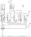
- FIG. 7shows a DMA engine, to be described more fully below, consistent with the present invention.
- the DMA enginecontains a register block 710 containing registers 712 for each channel in the subsystem where each channel represents a peripheral device 232 - 236 .
- the register blockcontain registers for 16 channels.
- FIG. 8shows a set of registers for one embodiment of the register block shown in FIG. 7 712 .
- Each registercontains a pointer to a location of the current processed descriptor for a channel.
- the DMAdetermines, based on the information contained in the register block, where to look for the appropriate descriptor.
- the register blockwill contain an active descriptor 714 providing the active descriptor information for the data being processed.
- a descriptorsimilar to that shown in FIG. 5 , will be loaded in DMA engine to facilitate processing of that channel. From the descriptor shown in FIG. 5 , the location of the data segment described by the descriptor 500 is from start location D898F000 to end location D898FFF as provided by registers 540 550 in the descriptor 500 .
- Descriptor 500advantageously contains the next descriptor address 530 in the memory space 240 of the next descriptor to be processed for the channel.
- FIG. 9shows a flow diagram indication one embodiment of the interleaving of the present invention.
- a subsystem processorprior to usage of the DMA, a subsystem processor will initialize each channel for use. For example, in one embodiment, the subsystem processor 210 will set active bits in the configuration register 510 for all channels to inactive. In one embodiment, when a channel is ready for processing, the subsystem processor 210 will load the descriptors for the channel and activate the channel 910 . The DMA engine 220 will then process the first descriptor. That is, the DMA engine 220 will begin transferring the data from the appropriate source location to the appropriate destination location.
- the DMA engine 220is meant to describe a broad range of DMA engines known in the art or to be developed.
- the method of transferring data from source to destinationwill not be described further.
- the datais transferred until either the descriptor is completely processed 940 or a segment subset (burst) length is processed 950 . If the segment subset length is reached, then the location where the current transfer ends is updated and saved 960 .
- the D898F000assume that after starting the initial processing of the D898F000, 64 bytes are transferred until the segment subset size is met. In this case, the next byte to be transferred would be D898F080.
- this new addressis saved to the start address 540 for the channel and thus the descriptor is updated.
- This descriptoris then saved 960 such that when the descriptor is loaded when this channel is to be further processed, the proper starting location will be loaded.
- a descriptor for the next channel active for processingas indicated in one embodiment by an active bit in the configuration register, will be fetched 920 and processing begins by the DMA engine on the segment represented by the newly loaded descriptor 930 .
- the next descriptor address 530is saved so that the next descriptor can be fetched and processed when the channel is next serviced 980 .
- the end address for the segment, D898FFFF 550is processed.
- the address of the next descriptor for the current channelis obtained from the next descriptor address field 530 of the current descriptor. In the embodiment shown, address 29872200 is then saved 980 . If a descriptor has completed its processing 940 , and there are no more descriptors available for the channel 970 , the channel is deactivated by the DMA engine 990 .
- the present inventionadvantageously reduces the required interaction of the subsystem processor in the ongoing operation of the DMA.
- the subsystem processoris provided with additional bandwidth for handling other subsystem functionality, while at the same time, the subsystem is only burdened with the circuitry for a single DMA engine.
- FIG. 7a block diagram of one embodiment of a DMA consistent with the present invention is shown.
- the DMAis notified of a subsystem DMA reset via reset signal 762 .
- a boot control state machine 760assumes control of the bus.
- the boot state machine 760waits for a notification 764 from the DTU 260 that a configuration packet has been received.
- the boot control 760then reads the configuration packet from the DTU 260 and, in accordance with the location information therein, sets up DMA registers for transfer of boot code from a location outside of the subsystem 200 to the instruction memory 250 .
- boot control logic 760Upon completion of the transfer of the boot code, boot control logic 760 notifies control processor 102 of the completion and relinquishes control of the subsystem bus 280 to the subsystem processor. In response to this notification, the control processor 102 can take the subsystem processor 210 out of its reset state.
- the descriptor write back logic 750interacts with the read/write control 730 to perform the saving the of the descriptor information as previously discussed. With the exception of the interaction of the read/write control 730 and address generation 740 required to aid in the aforementioned advantageous functions described herein, these portions perform there functions know in the art and will not be described further.
Landscapes
- Engineering & Computer Science (AREA)
- Theoretical Computer Science (AREA)
- Physics & Mathematics (AREA)
- General Engineering & Computer Science (AREA)
- General Physics & Mathematics (AREA)
- Computer Hardware Design (AREA)
- Mathematical Physics (AREA)
- Computer Security & Cryptography (AREA)
- Software Systems (AREA)
- Bus Control (AREA)
- Storage Device Security (AREA)
Abstract
Description
Claims (20)
Priority Applications (1)
| Application Number | Priority Date | Filing Date | Title |
|---|---|---|---|
| US10/469,529US7653763B2 (en) | 2001-02-28 | 2002-02-28 | Subsystem boot and peripheral data transfer architecture for a subsystem of a system-on- chip |
Applications Claiming Priority (3)
| Application Number | Priority Date | Filing Date | Title |
|---|---|---|---|
| US27243901P | 2001-02-28 | 2001-02-28 | |
| US10/469,529US7653763B2 (en) | 2001-02-28 | 2002-02-28 | Subsystem boot and peripheral data transfer architecture for a subsystem of a system-on- chip |
| PCT/US2002/006331WO2002069157A1 (en) | 2001-02-28 | 2002-02-28 | A subsystem boot and peripheral data transfer architecture for a subsystem of a system-on-chip |
Publications (2)
| Publication Number | Publication Date |
|---|---|
| US20040186930A1 US20040186930A1 (en) | 2004-09-23 |
| US7653763B2true US7653763B2 (en) | 2010-01-26 |
Family
ID=23039795
Family Applications (7)
| Application Number | Title | Priority Date | Filing Date |
|---|---|---|---|
| US10/086,938AbandonedUS20020161978A1 (en) | 2001-02-28 | 2002-02-28 | Multi-service system-on-chip including on-chip memory with multiple access path |
| US10/469,529Expired - Fee RelatedUS7653763B2 (en) | 2001-02-28 | 2002-02-28 | Subsystem boot and peripheral data transfer architecture for a subsystem of a system-on- chip |
| US10/469,467Expired - Fee RelatedUS7436954B2 (en) | 2001-02-28 | 2002-02-28 | Security system with an intelligent DMA controller |
| US10/086,953Expired - Fee RelatedUS7095752B2 (en) | 2001-02-28 | 2002-02-28 | On-chip inter-subsystem communication including concurrent data traffic routing |
| US10/086,665Expired - LifetimeUS7096292B2 (en) | 2001-02-28 | 2002-02-28 | On-chip inter-subsystem communication |
| US11/422,373Expired - LifetimeUS7243179B2 (en) | 2001-02-28 | 2006-06-06 | On-chip inter-subsystem communication |
| US11/424,787Expired - Fee RelatedUS7349424B2 (en) | 2001-02-28 | 2006-06-16 | On-chip inter-subsystem communication including concurrent data traffic routing |
Family Applications Before (1)
| Application Number | Title | Priority Date | Filing Date |
|---|---|---|---|
| US10/086,938AbandonedUS20020161978A1 (en) | 2001-02-28 | 2002-02-28 | Multi-service system-on-chip including on-chip memory with multiple access path |
Family Applications After (5)
| Application Number | Title | Priority Date | Filing Date |
|---|---|---|---|
| US10/469,467Expired - Fee RelatedUS7436954B2 (en) | 2001-02-28 | 2002-02-28 | Security system with an intelligent DMA controller |
| US10/086,953Expired - Fee RelatedUS7095752B2 (en) | 2001-02-28 | 2002-02-28 | On-chip inter-subsystem communication including concurrent data traffic routing |
| US10/086,665Expired - LifetimeUS7096292B2 (en) | 2001-02-28 | 2002-02-28 | On-chip inter-subsystem communication |
| US11/422,373Expired - LifetimeUS7243179B2 (en) | 2001-02-28 | 2006-06-06 | On-chip inter-subsystem communication |
| US11/424,787Expired - Fee RelatedUS7349424B2 (en) | 2001-02-28 | 2006-06-16 | On-chip inter-subsystem communication including concurrent data traffic routing |
Country Status (3)
| Country | Link |
|---|---|
| US (7) | US20020161978A1 (en) |
| AU (1) | AU2002252173A1 (en) |
| WO (3) | WO2002069157A1 (en) |
Families Citing this family (53)
| Publication number | Priority date | Publication date | Assignee | Title |
|---|---|---|---|---|
| US20020161978A1 (en)* | 2001-02-28 | 2002-10-31 | George Apostol | Multi-service system-on-chip including on-chip memory with multiple access path |
| US6816938B2 (en)* | 2001-03-27 | 2004-11-09 | Synopsys, Inc. | Method and apparatus for providing a modular system on-chip interface |
| US7039750B1 (en)* | 2001-07-24 | 2006-05-02 | Plx Technology, Inc. | On-chip switch fabric |
| JP3996010B2 (en)* | 2002-08-01 | 2007-10-24 | 株式会社日立製作所 | Storage network system, management apparatus, management method and program |
| US7107381B2 (en)* | 2002-11-20 | 2006-09-12 | Pmc-Sierra, Inc. | Flexible data transfer to and from external device of system-on-chip |
| US20040225707A1 (en)* | 2003-05-09 | 2004-11-11 | Chong Huai-Ter Victor | Systems and methods for combining a slow data stream and a fast data stream into a single fast data stream |
| US7065602B2 (en)* | 2003-07-01 | 2006-06-20 | International Business Machines Corporation | Circuit and method for pipelined insertion |
| DE10337699B4 (en)* | 2003-08-16 | 2006-01-12 | Phoenix Contact Gmbh & Co. Kg | Method and device for transmitting data over a bus network using the broadcast principle |
| US7091743B2 (en)* | 2003-10-07 | 2006-08-15 | International Business Machines Corporation | Data acknowledgment using impedance mismatching |
| TWI269165B (en) | 2004-03-30 | 2006-12-21 | Infortrend Technology Inc | Dispatching of service requests in redundant storage virtualization subsystems |
| JP4212508B2 (en)* | 2004-04-14 | 2009-01-21 | 株式会社東芝 | Packet generator |
| JP4222251B2 (en)* | 2004-04-27 | 2009-02-12 | ソニー株式会社 | Bus arbitration apparatus and bus arbitration method |
| WO2006030650A1 (en)* | 2004-09-16 | 2006-03-23 | Nec Corporation | Information processing device having a plurality of processing units sharing a resource |
| US7269682B2 (en)* | 2005-08-11 | 2007-09-11 | P.A. Semi, Inc. | Segmented interconnect for connecting multiple agents in a system |
| US7467295B2 (en)* | 2005-10-07 | 2008-12-16 | International Business Machines Corporation | Determining a boot image based on a requesting client address |
| EP1801700B1 (en)* | 2005-12-23 | 2013-06-26 | Texas Instruments Inc. | Method and systems to restrict usage of a DMA channel |
| EP1971925A4 (en)* | 2005-12-23 | 2009-01-07 | Texas Instruments Inc | Methods and systems to restrict usage of a dma channel |
| US20080077720A1 (en)* | 2006-09-27 | 2008-03-27 | Blaise Fanning | Isochronous memory access with variable channel priorities and timers |
| US8122078B2 (en) | 2006-10-06 | 2012-02-21 | Calos Fund, LLC | Processor with enhanced combined-arithmetic capability |
| US7870313B2 (en)* | 2007-02-27 | 2011-01-11 | Integrated Device Technology, Inc. | Method and structure to support system resource access of a serial device implementating a lite-weight protocol |
| US8094677B2 (en)* | 2007-02-27 | 2012-01-10 | Integrated Device Technology, Inc. | Multi-bus structure for optimizing system performance of a serial buffer |
| US20080209089A1 (en)* | 2007-02-27 | 2008-08-28 | Integrated Device Technology, Inc. | Packet-Based Parallel Interface Protocol For A Serial Buffer Having A Parallel Processor Port |
| US8185899B2 (en)* | 2007-03-07 | 2012-05-22 | International Business Machines Corporation | Prediction based priority scheduling |
| US8204225B2 (en)* | 2007-07-23 | 2012-06-19 | Savi Technology, Inc. | Method and apparatus for providing security in a radio frequency identification system |
| US20090055639A1 (en)* | 2007-08-20 | 2009-02-26 | Kimmo Kuusilinna | Methods and system for modular device booting |
| IL187038A0 (en)* | 2007-10-30 | 2008-02-09 | Sandisk Il Ltd | Secure data processing for unaligned data |
| US7966271B2 (en)* | 2008-05-12 | 2011-06-21 | Microsoft Corporation | Device influenced table formatting |
| US20100125717A1 (en)* | 2008-11-17 | 2010-05-20 | Mois Navon | Synchronization Controller For Multiple Multi-Threaded Processors |
| US20110093099A1 (en)* | 2009-10-16 | 2011-04-21 | Newport Controls | Controller system adapted for spa |
| US20110179212A1 (en)* | 2010-01-20 | 2011-07-21 | Charles Andrew Hartman | Bus arbitration for sideband signals |
| US8307138B2 (en)* | 2010-07-12 | 2012-11-06 | Arm Limited | Apparatus and method for controlling issuing of transaction requests |
| US8904115B2 (en) | 2010-09-28 | 2014-12-02 | Texas Instruments Incorporated | Cache with multiple access pipelines |
| GB2493340A (en)* | 2011-07-28 | 2013-02-06 | St Microelectronics Res & Dev | Address mapping of boot transactions between dies in a system in package |
| WO2013100783A1 (en) | 2011-12-29 | 2013-07-04 | Intel Corporation | Method and system for control signalling in a data path module |
| US9658975B2 (en)* | 2012-07-31 | 2017-05-23 | Silicon Laboratories Inc. | Data transfer manager |
| CN103518205B (en)* | 2013-03-27 | 2016-08-10 | 华为技术有限公司 | Method and automation equipment for restricting operation authority |
| US10331583B2 (en) | 2013-09-26 | 2019-06-25 | Intel Corporation | Executing distributed memory operations using processing elements connected by distributed channels |
| US20160300232A1 (en)* | 2013-11-13 | 2016-10-13 | Rakuten, Inc. | Monitoring assistance device |
| US9939869B2 (en) | 2015-03-13 | 2018-04-10 | Qualcomm Incorporated | Methods and systems for coordination of operating states amongst multiple SOCs within a computing device |
| US10303631B2 (en) | 2016-03-17 | 2019-05-28 | International Business Machines Corporation | Self-moderating bus arbitration architecture |
| US11086816B2 (en) | 2017-09-28 | 2021-08-10 | Intel Corporation | Processors, methods, and systems for debugging a configurable spatial accelerator |
| WO2019144267A1 (en)* | 2018-01-23 | 2019-08-01 | 深圳市大疆创新科技有限公司 | Chip, processor, computer system, and mobile device |
| IL315283A (en) | 2018-03-30 | 2024-10-01 | Google Llc | Mediation parts of transactions in ritualistic channels attributed to connection |
| WO2019191431A1 (en) | 2018-03-30 | 2019-10-03 | Provino Technologies, Inc. | PROTOCOL LEVEL CONTROL FOR SYSTEM ON A CHIP (SoC) AGENT RESET AND POWER MANAGEMENT |
| US11307873B2 (en) | 2018-04-03 | 2022-04-19 | Intel Corporation | Apparatus, methods, and systems for unstructured data flow in a configurable spatial accelerator with predicate propagation and merging |
| US10891240B2 (en) | 2018-06-30 | 2021-01-12 | Intel Corporation | Apparatus, methods, and systems for low latency communication in a configurable spatial accelerator |
| US11200186B2 (en) | 2018-06-30 | 2021-12-14 | Intel Corporation | Apparatuses, methods, and systems for operations in a configurable spatial accelerator |
| US10678724B1 (en) | 2018-12-29 | 2020-06-09 | Intel Corporation | Apparatuses, methods, and systems for in-network storage in a configurable spatial accelerator |
| US10915471B2 (en) | 2019-03-30 | 2021-02-09 | Intel Corporation | Apparatuses, methods, and systems for memory interface circuit allocation in a configurable spatial accelerator |
| US10817291B2 (en) | 2019-03-30 | 2020-10-27 | Intel Corporation | Apparatuses, methods, and systems for swizzle operations in a configurable spatial accelerator |
| US11037050B2 (en) | 2019-06-29 | 2021-06-15 | Intel Corporation | Apparatuses, methods, and systems for memory interface circuit arbitration in a configurable spatial accelerator |
| US12086080B2 (en) | 2020-09-26 | 2024-09-10 | Intel Corporation | Apparatuses, methods, and systems for a configurable accelerator having dataflow execution circuits |
| CN114385528B (en) | 2020-10-16 | 2024-11-29 | 瑞昱半导体股份有限公司 | Direct memory access controller, electronic device using the same, and method of operating the same |
Citations (49)
| Publication number | Priority date | Publication date | Assignee | Title |
|---|---|---|---|---|
| US4352952A (en) | 1978-06-12 | 1982-10-05 | Motorola Inc. | Data security module |
| US4697262A (en) | 1984-12-20 | 1987-09-29 | Siemens Aktiengesellschaft | Digital carrier channel bus interface module for a multiplexer having a cross-connect bus system |
| US5185864A (en) | 1989-06-16 | 1993-02-09 | International Business Machines Corporation | Interrupt handling for a computing system with logical devices and interrupt reset |
| US5197130A (en) | 1989-12-29 | 1993-03-23 | Supercomputer Systems Limited Partnership | Cluster architecture for a highly parallel scalar/vector multiprocessor system |
| US5222223A (en) | 1989-02-03 | 1993-06-22 | Digital Equipment Corporation | Method and apparatus for ordering and queueing multiple memory requests |
| US5224166A (en) | 1992-08-11 | 1993-06-29 | International Business Machines Corporation | System for seamless processing of encrypted and non-encrypted data and instructions |
| US5353417A (en)* | 1991-05-28 | 1994-10-04 | International Business Machines Corp. | Personal computer with bus interface controller coupled directly with local processor and input/output data buses and for anticipating memory control changes on arbitration for bus access |
| US5388261A (en)* | 1992-09-30 | 1995-02-07 | Apple Computer, Inc. | Apparatus and method for handling frame overruns in a digital signal processing system |
| US5606668A (en) | 1993-12-15 | 1997-02-25 | Checkpoint Software Technologies Ltd. | System for securing inbound and outbound data packet flow in a computer network |
| US5657472A (en) | 1995-03-31 | 1997-08-12 | Sun Microsystems, Inc. | Memory transaction execution system and method for multiprocessor system having independent parallel transaction queues associated with each processor |
| US5668813A (en) | 1995-07-17 | 1997-09-16 | Nat Semiconductor Corp | Dynamic synchronization code detection window |
| US5799207A (en) | 1995-03-28 | 1998-08-25 | Industrial Technology Research Institute | Non-blocking peripheral access architecture having a register configure to indicate a path selection for data transfer between a master, memory, and an I/O device |
| US5812799A (en) | 1995-06-07 | 1998-09-22 | Microunity Systems Engineering, Inc. | Non-blocking load buffer and a multiple-priority memory system for real-time multiprocessing |
| US5848367A (en)* | 1996-09-13 | 1998-12-08 | Sony Corporation | System and method for sharing a non-volatile memory element as a boot device |
| US5905876A (en) | 1996-12-16 | 1999-05-18 | Intel Corporation | Queue ordering for memory and I/O transactions in a multiple concurrent transaction computer system |
| US6021201A (en) | 1997-01-07 | 2000-02-01 | Intel Corporation | Method and apparatus for integrated ciphering and hashing |
| US6028939A (en) | 1997-01-03 | 2000-02-22 | Redcreek Communications, Inc. | Data security system and method |
| US6034542A (en) | 1997-10-14 | 2000-03-07 | Xilinx, Inc. | Bus structure for modularized chip with FPGA modules |
| US6058474A (en)* | 1997-01-24 | 2000-05-02 | Texas Instruments Incorporated | Method and apparatus for DMA boot loading a microprocessor without an internal ROM |
| US6081852A (en)* | 1996-04-26 | 2000-06-27 | Texas Instruments Incorporated | Packet data transferring system for autonomously operating a DMA by autonomous boot mode select signal wherein the DMA is enabled to at least one program control list |
| US6118462A (en) | 1997-07-01 | 2000-09-12 | Memtrax Llc | Computer system controller having internal memory and external memory control |
| US6122690A (en) | 1997-06-05 | 2000-09-19 | Mentor Graphics Corporation | On-chip bus architecture that is both processor independent and scalable |
| US6185520B1 (en) | 1998-05-22 | 2001-02-06 | 3Com Corporation | Method and system for bus switching data transfers |
| WO2001018997A1 (en) | 1999-09-10 | 2001-03-15 | Fantasma Networks, Inc. | Baseband wireless network for isochronous communication |
| US6247084B1 (en)* | 1997-10-08 | 2001-06-12 | Lsi Logic Corporation | Integrated circuit with unified memory system and dual bus architecture |
| US20010026439A1 (en) | 1998-08-31 | 2001-10-04 | Micron Technology, Inc. | Structure and method for an electronic assembly |
| US6317803B1 (en) | 1996-03-29 | 2001-11-13 | Intel Corporation | High-throughput interconnect having pipelined and non-pipelined bus transaction modes |
| US6321285B1 (en) | 1997-05-27 | 2001-11-20 | Fusion Micromedia Corporation | Bus arrangements for interconnection of discrete and/or integrated modules in a digital system and associated method |
| US6321318B1 (en)* | 1997-12-31 | 2001-11-20 | Texas Instruments Incorporated | User-configurable on-chip program memory system |
| US20010049726A1 (en) | 2000-06-02 | 2001-12-06 | Guillaume Comeau | Data path engine |
| US6347344B1 (en) | 1998-10-14 | 2002-02-12 | Hitachi, Ltd. | Integrated multimedia system with local processor, data transfer switch, processing modules, fixed functional unit, data streamer, interface unit and multiplexer, all integrated on multimedia processor |
| US20020069354A1 (en)* | 2000-02-03 | 2002-06-06 | Fallon James J. | Systems and methods for accelerated loading of operating systems and application programs |
| US6473810B1 (en)* | 1998-09-28 | 2002-10-29 | Texas Instruments Incorporated | Circuits, systems, and methods for efficient wake up of peripheral component interconnect controller |
| USRE37980E1 (en) | 1996-12-31 | 2003-02-04 | Compaq Computer Corporation | Bus-to-bus bridge in computer system, with fast burst memory range |
| US6549965B1 (en)* | 1998-04-29 | 2003-04-15 | Stmicroelectronics Limited | Microcomputer with interrupt packets |
| US6557078B1 (en) | 2000-02-21 | 2003-04-29 | Hewlett Packard Development Company, L.P. | Cache chain structure to implement high bandwidth low latency cache memory subsystem |
| US6560160B1 (en) | 2000-11-13 | 2003-05-06 | Agilent Technologies, Inc. | Multi-port memory that sequences port accesses |
| US20030188118A1 (en)* | 2000-09-27 | 2003-10-02 | Jackson Gregor Said | System and method to improve speed and reduce memory allocation for set top box boot-up |
| US20030189573A1 (en) | 1999-08-27 | 2003-10-09 | Dahlen Eric J. | Method and apparatus for command translation and enforcement of ordering of commands |
| US6675243B1 (en)* | 1999-03-17 | 2004-01-06 | Adaptec, Inc. | Methods and apparatus for implementing a device side advanced serial protocol |
| US6681270B1 (en) | 1999-12-07 | 2004-01-20 | Texas Instruments Incorporated | Effective channel priority processing for transfer controller with hub and ports |
| US20040128144A1 (en)* | 1998-09-25 | 2004-07-01 | Johnson Christopher Sean | Prompt management method supporting multiple languages in a system having a multi-bus structure and controlled by remotely generated commands |
| US6784890B1 (en) | 1998-03-02 | 2004-08-31 | Intel Corporation | Accelerated graphics port expedite cycle throttling control mechanism |
| US20040172490A1 (en)* | 2001-04-11 | 2004-09-02 | Mark Stadler | Reduced-overhead dma |
| US20040250056A1 (en)* | 2003-06-03 | 2004-12-09 | Christopher Chang | System boot method |
| US7020763B2 (en)* | 2000-03-08 | 2006-03-28 | Sun Microsystems, Inc. | Computer processing architecture having a scalable number of processing paths and pipelines |
| US7035966B2 (en)* | 2001-08-30 | 2006-04-25 | Micron Technology, Inc. | Processing system with direct memory transfer |
| US7237105B2 (en)* | 2003-05-07 | 2007-06-26 | International Business Machines Corporation | Startup system and method using boot code |
| US7296143B2 (en)* | 2004-06-22 | 2007-11-13 | Lenovo (Singapore) Pte. Ltd. | Method and system for loading processor boot code from serial flash memory |
Family Cites Families (8)
| Publication number | Priority date | Publication date | Assignee | Title |
|---|---|---|---|---|
| US4245306A (en)* | 1978-12-21 | 1981-01-13 | Burroughs Corporation | Selection of addressed processor in a multi-processor network |
| KR0181471B1 (en)* | 1990-07-27 | 1999-05-15 | 윌리암 피.브레이든 | Computer data routing system |
| US5535417A (en)* | 1993-09-27 | 1996-07-09 | Hitachi America, Inc. | On-chip DMA controller with host computer interface employing boot sequencing and address generation schemes |
| US5920566A (en)* | 1997-06-30 | 1999-07-06 | Sun Microsystems, Inc. | Routing in a multi-layer distributed network element |
| US6312285B1 (en)* | 1999-02-25 | 2001-11-06 | Molex Incorporated | Panel mounting system for electrical connectors |
| US20020161978A1 (en)* | 2001-02-28 | 2002-10-31 | George Apostol | Multi-service system-on-chip including on-chip memory with multiple access path |
| US6677786B2 (en)* | 2001-02-28 | 2004-01-13 | Brecis Communications Corporation | Multi-service processor clocking system |
| US7107381B2 (en)* | 2002-11-20 | 2006-09-12 | Pmc-Sierra, Inc. | Flexible data transfer to and from external device of system-on-chip |
- 2002
- 2002-02-28USUS10/086,938patent/US20020161978A1/ennot_activeAbandoned
- 2002-02-28WOPCT/US2002/006331patent/WO2002069157A1/ennot_activeApplication Discontinuation
- 2002-02-28WOPCT/US2002/006383patent/WO2002069158A1/ennot_activeApplication Discontinuation
- 2002-02-28AUAU2002252173Apatent/AU2002252173A1/ennot_activeAbandoned
- 2002-02-28USUS10/469,529patent/US7653763B2/ennot_activeExpired - Fee Related
- 2002-02-28USUS10/469,467patent/US7436954B2/ennot_activeExpired - Fee Related
- 2002-02-28WOPCT/US2002/006384patent/WO2002069115A2/ennot_activeApplication Discontinuation
- 2002-02-28USUS10/086,953patent/US7095752B2/ennot_activeExpired - Fee Related
- 2002-02-28USUS10/086,665patent/US7096292B2/ennot_activeExpired - Lifetime
- 2006
- 2006-06-06USUS11/422,373patent/US7243179B2/ennot_activeExpired - Lifetime
- 2006-06-16USUS11/424,787patent/US7349424B2/ennot_activeExpired - Fee Related
Patent Citations (50)
| Publication number | Priority date | Publication date | Assignee | Title |
|---|---|---|---|---|
| US4352952A (en) | 1978-06-12 | 1982-10-05 | Motorola Inc. | Data security module |
| US4697262A (en) | 1984-12-20 | 1987-09-29 | Siemens Aktiengesellschaft | Digital carrier channel bus interface module for a multiplexer having a cross-connect bus system |
| US5222223A (en) | 1989-02-03 | 1993-06-22 | Digital Equipment Corporation | Method and apparatus for ordering and queueing multiple memory requests |
| US5185864A (en) | 1989-06-16 | 1993-02-09 | International Business Machines Corporation | Interrupt handling for a computing system with logical devices and interrupt reset |
| US5197130A (en) | 1989-12-29 | 1993-03-23 | Supercomputer Systems Limited Partnership | Cluster architecture for a highly parallel scalar/vector multiprocessor system |
| US5353417A (en)* | 1991-05-28 | 1994-10-04 | International Business Machines Corp. | Personal computer with bus interface controller coupled directly with local processor and input/output data buses and for anticipating memory control changes on arbitration for bus access |
| US5224166A (en) | 1992-08-11 | 1993-06-29 | International Business Machines Corporation | System for seamless processing of encrypted and non-encrypted data and instructions |
| US5388261A (en)* | 1992-09-30 | 1995-02-07 | Apple Computer, Inc. | Apparatus and method for handling frame overruns in a digital signal processing system |
| US5606668A (en) | 1993-12-15 | 1997-02-25 | Checkpoint Software Technologies Ltd. | System for securing inbound and outbound data packet flow in a computer network |
| US5799207A (en) | 1995-03-28 | 1998-08-25 | Industrial Technology Research Institute | Non-blocking peripheral access architecture having a register configure to indicate a path selection for data transfer between a master, memory, and an I/O device |
| US5657472A (en) | 1995-03-31 | 1997-08-12 | Sun Microsystems, Inc. | Memory transaction execution system and method for multiprocessor system having independent parallel transaction queues associated with each processor |
| US5812799A (en) | 1995-06-07 | 1998-09-22 | Microunity Systems Engineering, Inc. | Non-blocking load buffer and a multiple-priority memory system for real-time multiprocessing |
| US5668813A (en) | 1995-07-17 | 1997-09-16 | Nat Semiconductor Corp | Dynamic synchronization code detection window |
| US6317803B1 (en) | 1996-03-29 | 2001-11-13 | Intel Corporation | High-throughput interconnect having pipelined and non-pipelined bus transaction modes |
| US6081852A (en)* | 1996-04-26 | 2000-06-27 | Texas Instruments Incorporated | Packet data transferring system for autonomously operating a DMA by autonomous boot mode select signal wherein the DMA is enabled to at least one program control list |
| US5848367A (en)* | 1996-09-13 | 1998-12-08 | Sony Corporation | System and method for sharing a non-volatile memory element as a boot device |
| US5905876A (en) | 1996-12-16 | 1999-05-18 | Intel Corporation | Queue ordering for memory and I/O transactions in a multiple concurrent transaction computer system |
| USRE37980E1 (en) | 1996-12-31 | 2003-02-04 | Compaq Computer Corporation | Bus-to-bus bridge in computer system, with fast burst memory range |
| US6028939A (en) | 1997-01-03 | 2000-02-22 | Redcreek Communications, Inc. | Data security system and method |
| US6021201A (en) | 1997-01-07 | 2000-02-01 | Intel Corporation | Method and apparatus for integrated ciphering and hashing |
| US6778667B1 (en) | 1997-01-07 | 2004-08-17 | Intel Corporation | Method and apparatus for integrated ciphering and hashing |
| US6058474A (en)* | 1997-01-24 | 2000-05-02 | Texas Instruments Incorporated | Method and apparatus for DMA boot loading a microprocessor without an internal ROM |
| US6321285B1 (en) | 1997-05-27 | 2001-11-20 | Fusion Micromedia Corporation | Bus arrangements for interconnection of discrete and/or integrated modules in a digital system and associated method |
| US6122690A (en) | 1997-06-05 | 2000-09-19 | Mentor Graphics Corporation | On-chip bus architecture that is both processor independent and scalable |
| US6118462A (en) | 1997-07-01 | 2000-09-12 | Memtrax Llc | Computer system controller having internal memory and external memory control |
| US6247084B1 (en)* | 1997-10-08 | 2001-06-12 | Lsi Logic Corporation | Integrated circuit with unified memory system and dual bus architecture |
| US6034542A (en) | 1997-10-14 | 2000-03-07 | Xilinx, Inc. | Bus structure for modularized chip with FPGA modules |
| US6321318B1 (en)* | 1997-12-31 | 2001-11-20 | Texas Instruments Incorporated | User-configurable on-chip program memory system |
| US6784890B1 (en) | 1998-03-02 | 2004-08-31 | Intel Corporation | Accelerated graphics port expedite cycle throttling control mechanism |
| US6549965B1 (en)* | 1998-04-29 | 2003-04-15 | Stmicroelectronics Limited | Microcomputer with interrupt packets |
| US6185520B1 (en) | 1998-05-22 | 2001-02-06 | 3Com Corporation | Method and system for bus switching data transfers |
| US20010026439A1 (en) | 1998-08-31 | 2001-10-04 | Micron Technology, Inc. | Structure and method for an electronic assembly |
| US20040128144A1 (en)* | 1998-09-25 | 2004-07-01 | Johnson Christopher Sean | Prompt management method supporting multiple languages in a system having a multi-bus structure and controlled by remotely generated commands |
| US6473810B1 (en)* | 1998-09-28 | 2002-10-29 | Texas Instruments Incorporated | Circuits, systems, and methods for efficient wake up of peripheral component interconnect controller |
| US6347344B1 (en) | 1998-10-14 | 2002-02-12 | Hitachi, Ltd. | Integrated multimedia system with local processor, data transfer switch, processing modules, fixed functional unit, data streamer, interface unit and multiplexer, all integrated on multimedia processor |
| US6675243B1 (en)* | 1999-03-17 | 2004-01-06 | Adaptec, Inc. | Methods and apparatus for implementing a device side advanced serial protocol |
| US20030189573A1 (en) | 1999-08-27 | 2003-10-09 | Dahlen Eric J. | Method and apparatus for command translation and enforcement of ordering of commands |
| WO2001018997A1 (en) | 1999-09-10 | 2001-03-15 | Fantasma Networks, Inc. | Baseband wireless network for isochronous communication |
| US6681270B1 (en) | 1999-12-07 | 2004-01-20 | Texas Instruments Incorporated | Effective channel priority processing for transfer controller with hub and ports |
| US20020069354A1 (en)* | 2000-02-03 | 2002-06-06 | Fallon James J. | Systems and methods for accelerated loading of operating systems and application programs |
| US6557078B1 (en) | 2000-02-21 | 2003-04-29 | Hewlett Packard Development Company, L.P. | Cache chain structure to implement high bandwidth low latency cache memory subsystem |
| US7020763B2 (en)* | 2000-03-08 | 2006-03-28 | Sun Microsystems, Inc. | Computer processing architecture having a scalable number of processing paths and pipelines |
| US20010049726A1 (en) | 2000-06-02 | 2001-12-06 | Guillaume Comeau | Data path engine |
| US20030188118A1 (en)* | 2000-09-27 | 2003-10-02 | Jackson Gregor Said | System and method to improve speed and reduce memory allocation for set top box boot-up |
| US6560160B1 (en) | 2000-11-13 | 2003-05-06 | Agilent Technologies, Inc. | Multi-port memory that sequences port accesses |
| US20040172490A1 (en)* | 2001-04-11 | 2004-09-02 | Mark Stadler | Reduced-overhead dma |
| US7035966B2 (en)* | 2001-08-30 | 2006-04-25 | Micron Technology, Inc. | Processing system with direct memory transfer |
| US7237105B2 (en)* | 2003-05-07 | 2007-06-26 | International Business Machines Corporation | Startup system and method using boot code |
| US20040250056A1 (en)* | 2003-06-03 | 2004-12-09 | Christopher Chang | System boot method |
| US7296143B2 (en)* | 2004-06-22 | 2007-11-13 | Lenovo (Singapore) Pte. Ltd. | Method and system for loading processor boot code from serial flash memory |
Also Published As
| Publication number | Publication date |
|---|---|
| US7436954B2 (en) | 2008-10-14 |
| US20060221931A1 (en) | 2006-10-05 |
| US7096292B2 (en) | 2006-08-22 |
| US20020161978A1 (en) | 2002-10-31 |
| US20020159474A1 (en) | 2002-10-31 |
| AU2002252173A1 (en) | 2002-09-12 |
| US7243179B2 (en) | 2007-07-10 |
| US20060212632A1 (en) | 2006-09-21 |
| WO2002069115A2 (en) | 2002-09-06 |
| WO2002069158A1 (en) | 2002-09-06 |
| US7349424B2 (en) | 2008-03-25 |
| US7095752B2 (en) | 2006-08-22 |
| WO2002069115A3 (en) | 2002-10-31 |
| WO2002069157A1 (en) | 2002-09-06 |
| US20040186930A1 (en) | 2004-09-23 |
| US20020161959A1 (en) | 2002-10-31 |
| US20050259823A1 (en) | 2005-11-24 |
Similar Documents
| Publication | Publication Date | Title |
|---|---|---|
| US7653763B2 (en) | Subsystem boot and peripheral data transfer architecture for a subsystem of a system-on- chip | |
| US6754735B2 (en) | Single descriptor scatter gather data transfer to or from a host processor | |
| US6701405B1 (en) | DMA handshake protocol | |
| US6954806B2 (en) | Data transfer apparatus and method | |
| US6356960B1 (en) | Microprocessor having an on-chip CPU fetching a debugging routine from a memory in an external debugging device in response to a control signal received through a debugging port | |
| US6473808B1 (en) | High performance communication controller for processing high speed data streams wherein execution of a task can be skipped if it involves fetching information from external memory bank | |
| US7496699B2 (en) | DMA descriptor queue read and cache write pointer arrangement | |
| US6301657B1 (en) | System and method for booting a computer | |
| US5752076A (en) | Dynamic programming of bus master channels by intelligent peripheral devices using communication packets | |
| US7512724B1 (en) | Multi-thread peripheral processing using dedicated peripheral bus | |
| JPH11338734A (en) | Computer system and method of operating the computer system | |
| US20030110364A1 (en) | Receiving data from interleaved multiple concurrent transactions in a FIFO memory | |
| WO2001006377A1 (en) | Multi-cast dma - a method for reducing bandwidth and processing overhead in digital systems | |
| KR20070049676A (en) | Method and apparatus for sending memory pre-fetch commands over a bus | |
| EP0464848B1 (en) | Structure for enabling direct memory-to-memory transfer | |
| JP2000010818A (en) | Computer system and method for operating the computer system | |
| US6687763B2 (en) | ATAPI command receiving method | |
| US6230215B1 (en) | On-demand transfer engine | |
| JP2000207247A (en) | Computer system and method of operating the computer system | |
| US6401191B1 (en) | System and method for remotely executing code | |
| EP1267269A2 (en) | Apparatus and method for distribution of signals from a high level data link controller to multiple digital signal processor cores | |
| US20070127484A1 (en) | Data transfer operations and buffer memories | |
| JP2000020488A (en) | Computer system and method for operating the same | |
| US6766383B1 (en) | Packet-based direct memory access | |
| US7194573B1 (en) | CAM-based search engine devices having advanced search and learn instruction handling |
Legal Events
| Date | Code | Title | Description |
|---|---|---|---|
| AS | Assignment | Owner name:BRECIS COMMUNICATIONS, CALIFORNIA Free format text:EMPLOYEE INVENTION ASSIGNMENT AND CONFIDENTIALITY AGREEMENT;ASSIGNOR:GREWAL, HARSIMRAN S.;REEL/FRAME:013119/0098 Effective date:19981116 | |
| AS | Assignment | Owner name:BRECIS COMMUICATIONS, CALIFORNIA Free format text:ASSIGNMENT OF ASSIGNORS INTEREST;ASSIGNORS:GADKARI, MILEEND;APOSTOL JR., GEORGE;REEL/FRAME:013118/0937 Effective date:20020530 | |
| AS | Assignment | Owner name:TRANSAMERICA TECHNOLOGY FINANCE CORPORATION, CONNE Free format text:SECURITY AGREEMENT;ASSIGNOR:BRECIS COMMUNICATIONS CORPORATION;REEL/FRAME:014172/0322 Effective date:20030613 | |
| AS | Assignment | Owner name:BRECIS COMMUNICATIONS CORPORATION, CALIFORNIA Free format text:ASSIGNMENT OF ASSIGNORS INTEREST;ASSIGNORS:GADKARI, MILEEND;APOSTOL, GEORGE JR.;REEL/FRAME:014936/0955 Effective date:20030827 Owner name:BRECIS COMMUNICATIONS CORPORATION, CALIFORNIA Free format text:EMPLOYEE INVENTION ASSIGNMENT AND CONFIDENTIALITY AGREEMENT AND CETIFICATE OF AMENDMENT OF ARTICLES OF INCORPORATION;ASSIGNOR:GREWAL, HARSIMARAN S.;REEL/FRAME:014940/0473 Effective date:19981116 | |
| AS | Assignment | Owner name:CAVIUM ACQUISITION CORP., CALIFORNIA Free format text:ASSIGNMENT OF ASSIGNORS INTEREST;ASSIGNOR:BRECIS COMMUNICATIONS CORPORATION;REEL/FRAME:015117/0933 Effective date:20040815 | |
| AS | Assignment | Owner name:BRECIS COMMUNICATIONS CORPORATION, CALIFORNIA Free format text:RELEASE OF SECURITY AGREEMENT;ASSIGNOR:TRANSAMERICA TECHNOLOGY FINANCE CORPORATION;REEL/FRAME:015271/0223 Effective date:20040304 | |
| AS | Assignment | Owner name:BRECIS COMMUNICATIONS CORP., CALIFORNIA Free format text:TERMINATION OF SECURITY AGREEMENT;ASSIGNOR:TRANSAMERICA TECHNOLOGY FINANCE CORPORATION;REEL/FRAME:016824/0393 Effective date:20040722 | |
| AS | Assignment | Owner name:CAVIUM NETWORKS, INC., CALIFORNIA Free format text:MERGER;ASSIGNOR:CAVIUM ACQUISITION CORP.;REEL/FRAME:019340/0001 Effective date:20070516 | |
| STCF | Information on status: patent grant | Free format text:PATENTED CASE | |
| CC | Certificate of correction | ||
| AS | Assignment | Owner name:CAVIUM, INC., CALIFORNIA Free format text:MERGER;ASSIGNOR:CAVIUM NETWORKS, INC.;REEL/FRAME:026632/0672 Effective date:20110617 | |
| FEPP | Fee payment procedure | Free format text:PAT HOLDER NO LONGER CLAIMS SMALL ENTITY STATUS, ENTITY STATUS SET TO UNDISCOUNTED (ORIGINAL EVENT CODE: STOL); ENTITY STATUS OF PATENT OWNER: LARGE ENTITY | |
| REFU | Refund | Free format text:REFUND - SURCHARGE, PETITION TO ACCEPT PYMT AFTER EXP, UNINTENTIONAL (ORIGINAL EVENT CODE: R2551); ENTITY STATUS OF PATENT OWNER: LARGE ENTITY | |
| FPAY | Fee payment | Year of fee payment:4 | |
| AS | Assignment | Owner name:JPMORGAN CHASE BANK, N.A., AS COLLATERAL AGENT, ILLINOIS Free format text:SECURITY AGREEMENT;ASSIGNORS:CAVIUM, INC.;CAVIUM NETWORKS LLC;REEL/FRAME:039715/0449 Effective date:20160816 Owner name:JPMORGAN CHASE BANK, N.A., AS COLLATERAL AGENT, IL Free format text:SECURITY AGREEMENT;ASSIGNORS:CAVIUM, INC.;CAVIUM NETWORKS LLC;REEL/FRAME:039715/0449 Effective date:20160816 | |
| FPAY | Fee payment | Year of fee payment:8 | |
| AS | Assignment | Owner name:CAVIUM, INC, CALIFORNIA Free format text:RELEASE BY SECURED PARTY;ASSIGNOR:JP MORGAN CHASE BANK, N.A., AS COLLATERAL AGENT;REEL/FRAME:046496/0001 Effective date:20180706 Owner name:QLOGIC CORPORATION, CALIFORNIA Free format text:RELEASE BY SECURED PARTY;ASSIGNOR:JP MORGAN CHASE BANK, N.A., AS COLLATERAL AGENT;REEL/FRAME:046496/0001 Effective date:20180706 Owner name:CAVIUM NETWORKS LLC, CALIFORNIA Free format text:RELEASE BY SECURED PARTY;ASSIGNOR:JP MORGAN CHASE BANK, N.A., AS COLLATERAL AGENT;REEL/FRAME:046496/0001 Effective date:20180706 | |
| AS | Assignment | Owner name:CAVIUM, LLC, CALIFORNIA Free format text:CERTIFICATE OF CONVERSION AND CERTIFICATE OF FORMATION;ASSIGNOR:CAVIUM, INC.;REEL/FRAME:047185/0422 Effective date:20180921 | |
| AS | Assignment | Owner name:CAVIUM INTERNATIONAL, CAYMAN ISLANDS Free format text:ASSIGNMENT OF ASSIGNORS INTEREST;ASSIGNOR:CAVIUM, LLC;REEL/FRAME:051948/0807 Effective date:20191231 | |
| AS | Assignment | Owner name:MARVELL ASIA PTE, LTD., SINGAPORE Free format text:ASSIGNMENT OF ASSIGNORS INTEREST;ASSIGNOR:CAVIUM INTERNATIONAL;REEL/FRAME:053179/0320 Effective date:20191231 | |
| FEPP | Fee payment procedure | Free format text:MAINTENANCE FEE REMINDER MAILED (ORIGINAL EVENT CODE: REM.); ENTITY STATUS OF PATENT OWNER: LARGE ENTITY | |
| LAPS | Lapse for failure to pay maintenance fees | Free format text:PATENT EXPIRED FOR FAILURE TO PAY MAINTENANCE FEES (ORIGINAL EVENT CODE: EXP.); ENTITY STATUS OF PATENT OWNER: LARGE ENTITY | |
| STCH | Information on status: patent discontinuation | Free format text:PATENT EXPIRED DUE TO NONPAYMENT OF MAINTENANCE FEES UNDER 37 CFR 1.362 | |
| FP | Lapsed due to failure to pay maintenance fee | Effective date:20220126 |