US7649483B1 - Communication driver - Google Patents
Communication driverDownload PDFInfo
- Publication number
- US7649483B1 US7649483B1US12/004,200US420007AUS7649483B1US 7649483 B1US7649483 B1US 7649483B1US 420007 AUS420007 AUS 420007AUS 7649483 B1US7649483 B1US 7649483B1
- Authority
- US
- United States
- Prior art keywords
- converters
- sets
- outputs
- signal
- ones
- Prior art date
- Legal status (The legal status is an assumption and is not a legal conclusion. Google has not performed a legal analysis and makes no representation as to the accuracy of the status listed.)
- Expired - Fee Related
Links
Images


Classifications
- H—ELECTRICITY
- H04—ELECTRIC COMMUNICATION TECHNIQUE
- H04L—TRANSMISSION OF DIGITAL INFORMATION, e.g. TELEGRAPHIC COMMUNICATION
- H04L25/00—Baseband systems
- H04L25/02—Details ; arrangements for supplying electrical power along data transmission lines
- H04L25/0264—Arrangements for coupling to transmission lines
- H04L25/0272—Arrangements for coupling to multiple lines, e.g. for differential transmission
- H—ELECTRICITY
- H03—ELECTRONIC CIRCUITRY
- H03M—CODING; DECODING; CODE CONVERSION IN GENERAL
- H03M1/00—Analogue/digital conversion; Digital/analogue conversion
- H03M1/66—Digital/analogue converters
- H03M1/661—Improving the reconstruction of the analogue output signal beyond the resolution of the digital input signal, e.g. by interpolation, by curve-fitting, by smoothing
- H—ELECTRICITY
- H04—ELECTRIC COMMUNICATION TECHNIQUE
- H04L—TRANSMISSION OF DIGITAL INFORMATION, e.g. TELEGRAPHIC COMMUNICATION
- H04L25/00—Baseband systems
- H04L25/02—Details ; arrangements for supplying electrical power along data transmission lines
- H04L25/03—Shaping networks in transmitter or receiver, e.g. adaptive shaping networks
- H04L25/03828—Arrangements for spectral shaping; Arrangements for providing signals with specified spectral properties
- H04L25/03834—Arrangements for spectral shaping; Arrangements for providing signals with specified spectral properties using pulse shaping
- H—ELECTRICITY
- H03—ELECTRONIC CIRCUITRY
- H03M—CODING; DECODING; CODE CONVERSION IN GENERAL
- H03M1/00—Analogue/digital conversion; Digital/analogue conversion
- H03M1/66—Digital/analogue converters
- H03M1/74—Simultaneous conversion
- H03M1/742—Simultaneous conversion using current sources as quantisation value generators
Definitions
- Non-Provisional patent application Ser. No. 10/191,924, filed Jul. 8, 2002(now U.S. Pat. No. 6,844,837), which is a continuation-in-part of U.S. Non-Provisional patent application Ser. No. 09/920,241, filed Aug. 1, 2001, and is a continuation-in-part of U.S. Non-Provisional patent application Ser. No. 09/737,474, filed Dec. 18, 2000 (now U.S. Pat. No. 6,462,688), and U.S. Non-Provisional patent application Ser. No. 10/972,143, filed Oct. 25, 2004, is a continuation-in-part of U.S. Non-Provisional patent application Ser. No. 09/737,743, filed Dec.
- the present inventionrelates generally to data communication. More particularly, the present invention relates to a Class B line driver for communication channels such as those present in an Ethernet network.
- a digital-to-analog converter(hereinafter a DAC) is generally an electronic circuit that receives an n-bit codeword from an interface and generates an analog voltage or current that is proportional to the codeword.
- DACDigital-To-Analog Converter
- the DAC of the U.S. Pat. No. 5,663,728 patentemploys a waveform shaping circuit to control the rise and fall times of each component waveform so that the analog waveform rising and falling edges settle to within a desired error bound of a linear output ramp.
- U.S. Pat. No. 5,936,450entitled A Waveshaping Circuit Using Digitally Controlled Weighted Current Summing, issued on Aug. 10, 1999, the contents of which are hereby incorporated by reference, discloses a waveshaping circuit.
- the waveshaping circuit of the U.S. Pat. No. 5,936,450 patentincludes a controller and a current summing circuit controlled by the controller.
- the current summing circuitryselectively sinks combinations of component currents in response to a sequence of control signal sets to generate an output current signal having a desired waveform.
- a signal outputmay include the output of a DAC and/or the output of one or more signal components within a DAC.
- a signal componentmay correspond to an individual bit of a codeword.
- One conventional methodgenerates a signal output with a slew rate controlled current source, as shown in FIG. 1 .
- the voltage V measured across a resistor Ris shown in FIG. 2 .
- the waveform Vincludes sharp transition areas (e.g., corners) 1 , 2 and 3 , which may introduce electromagnetic interference. Such interference may inhibit accurate signal processing.
- FIG. 3Another circuit which generates an output signal employs a current mirror 10 having an RC filter, as illustrated in FIG. 3 .
- a current source Idrives the current mirror 10 .
- Current mirror 10includes a first transistor 11 and a second transistor 12 .
- Transistors 11 and 12are preferably CMOS transistors.
- the first transistor 11includes gate-to-drain feedback, and is coupled to transistors 12 through the RC filter.
- the RC filterlimits rise and fall times of the input signal I.
- the R and C componentsare typically process and/or temperature dependent. Such dependence causes variation in the output waveform as shown in FIG. 4 .
- the dashed lines in FIG. 4represent arbitrary output responses due to temperature and/or process variation. A stable output signal is difficult to obtain with such a circuit.
- FIG. 5depicts a D/A circuit capable of producing such multi-level signals.
- the D/A circuit of FIG. 5employs a DAC 32 , a low pass filter 34 , an operational amplifier 36 , a transistor 38 , and a resistor 39 .
- Each level of a multilevel input signalis provided to DAC 32 for conversion to an analog signal.
- the LPF 34determines the rise time of the output of the DAC 32 , and the output is passed to operational amplifier 36 . This construction presents two problems.
- FIG. 24shows a waveform produced by the D/A circuit of FIG. 5 where DAC 32 has four levels. Because the bandwidth of the circuit is a function of the signal level provided to the non-inverting input of operational amplifier 36 , the slew rate differs for each signal level. Referring to FIG. 24 for example, the bandwidth for the transition from the 0 signal level to the 1 signal level is low, resulting in a low slew rate and a long rise time t 1 . In contrast, the bandwidth for the transition from the 2 signal level to the 3 signal level is high, resulting in a high slew rate and a short rise time t 2 .
- An Ethernet controllerincludes a decoder, and T sets of transmit circuits. Each set of transmit circuits receives one of T decoded signals from the decoder, and includes a digital-to-analog converter (DAC) that provides a transmit output signal, and a replica circuit that provides a replica output signal.
- Each DACincludes N current sources arranged in parallel and differentially, and M delay elements. Each current source includes a control input. A sum of outputs of the N current sources forms each transmit output signal. An input of the first delay element and the control input of the first current source receive a decoded signal. An input of an mth delay element is in communication with an output of an m ⁇ 1th delay element. The output of each delay element controls a corresponding control input of a current source. A sum of the transmit output signals forms an accumulated output signal.
- FIG. 1is a diagram of a conventional circuit, which includes a slew rate controlled current source.
- FIG. 2is a graphical depiction of a waveshape corresponding to an output of the FIG. 1 circuit.
- FIG. 3is a view of a conventional circuit including a current mirror having an RC filter.
- FIG. 4is a graphical depiction of a waveshape corresponding to an output of the FIG. 3 circuit.
- FIG. 5is a schematic block diagram of a D/A circuit.
- FIG. 6is a graphical depiction of a waveshape having smooth transition areas.
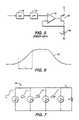
- FIG. 7is a circuit diagram of a current source according to the present invention.
- FIG. 8is a graphical depiction of current components of the current source illustrated in FIG. 6 .
- FIG. 9is a graphical depiction of a resultant output waveshape from the current source illustrated in FIGS. 6 and 7 .
- FIG. 10is a graphical depiction of a waveform template, and a waveshape that fits within the template.
- FIG. 11is a circuit diagram of a current source according to the present invention.
- FIGS. 12 a - 12 care graphical depictions of waveshapes generated by the current source of FIG. 10 .
- FIG. 13is a circuit diagram of a current source according to the present invention.
- FIG. 14is a circuit diagram of a current source having variable delay elements according to the present invention.
- FIG. 15 ais a graphical depiction of a waveform generated with uniform delay elements.
- FIG. 15 bis a graphical depiction of a waveform generated with non-uniform delay elements.
- FIG. 16is a circuit diagram of a current source including a plurality of differential transistor pairs according to the present invention.
- FIG. 17is a circuit diagram of an alternative embodiment according to the present invention.
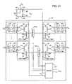
- FIG. 18is a high-level schematic diagram illustrating a communication channel in connection with which the method and apparatus of the present invention may be used;
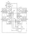
- FIG. 19is a detailed schematic diagram illustrating one embodiment of a transceiver according to the principles of the present invention.
- FIG. 20is a detailed schematic diagram illustrating a second embodiment of a transceiver according to the principles of the present invention.
- FIG. 21is a detailed schematic diagram illustrating a third embodiment of a transceiver according to the principles of the present invention.
- FIG. 22shows detail of a DAC according to some implementations.
- FIG. 23is a detailed schematic diagram illustrating a fourth embodiment of a transceiver according to the principles of the present invention.
- FIG. 24shows a waveform produced by the D/A circuit of FIG. 5 .
- FIG. 25shows a waveform produced by the circuit of FIG. 21 .
- FIG. 26shows detail of a converter according to one implementation.
- FIG. 27is a detailed schematic diagram illustrating a fifth embodiment of a transceiver according to the principles of the present invention.
- FIG. 28shows detail of converter according to one implementation.
- FIG. 29shows detail of a DAC according to some implementations.
- FIG. 30is a functional block diagram of a transceiver
- FIG. 31is a circuit diagram illustrating baseline correction to an active summer
- FIG. 32is a circuit diagram illustrating error correction.
- FIG. 33is a circuit diagram illustrating a summer that receives a transmitter signal, a replica transmitter signal and an output of a voltage to current converter.
- FIG. 34is a circuit diagram illustrating a summer that receives a transmitter signal, a replica transmitter signal and an output of a charge pump.
- the present inventionwill be described with respect to circuits and methods for shaping waveforms, and in particular, to a digital-to-analog converter (DAC) employing such a waveshaping circuit.
- DACdigital-to-analog converter
- the present inventionis not limited to applications involving DACs, but also may be applied to other applications, such as signal processing, systems to control signal rise/fall time, signal storage, communications, etc.
- the present inventionis particularly suited to applications in the read channel of a hard disk drive, many other applications will suggest themselves to persons of skill in the electrical engineering arts.
- the present inventionis particularly suitable for use with the structure described in U.S. patent application Ser. No. 09/737,743, entitled “Active Replica Transformer Hybrid,” filed concurrently herewith, the contents of which are incorporated herein by reference.
- FIG. 6illustrates a desired signal output 20 .
- the output waveform 20includes smooth transition areas, which reduce noise such as electromagnetic interference.
- a preferred rise time (“T r ”) for a DACis 3-5 nanoseconds (ns).
- current source 30includes a plurality of current sources.
- current source 30may include current sources I 1 , I 2 , I 3 and I 4 .
- Current sources I 1 , I 2 , I 3 and I 4each preferably generate a respective current I n , where n is 1, 2, 3 or so forth.
- the signals Inare preferably equal in magnitude and form, and may include a signal delay.
- current sources I neach generate a linear ramp. For example, consider a signal I 1 , which includes a linearly rising edge starting at time t 0 .
- Current I 2mirrors current I 1 , except that I 2 includes a linearly rising edge starting at time t 0 + ⁇ t.
- the variable ⁇ trepresents an amount of delay time.
- Current I 3mirrors currents I 1 and I 2 , except that current I 3 includes a linearly rising edge starting at time t 0 +2 ⁇ t.
- current I 4mirrors currents I 1 , I 2 , and I 3 , except that its linearly rising edge starts at time t 0 +3 ⁇ t.
- the relative waveform components for currents I 1 , I 2 , I 3 and I 4are shown in FIG. 8 .
- Waveform 10approximates the desired output signal shown in FIG. 6 .
- waveform I 0has many desirable properties.
- 10has selectable transition areas (corners). The transition areas can be smooth, or sharp, by selectively adjusting the length of ⁇ t.
- waveform I 0accommodates arbitrary rise/fall times.
- the waveform I 0can also be adjusted by varying ⁇ t to fit within specified requirements.
- waveform I 0can be adjusted to fit within a template 40 , for example, as provided by the IEEE standard waveform shape.
- 10has been optimized to produce low electromagnetic interference and to fit within the IEEE template 40 .
- the delay variable ⁇ tis preferably controlled using a delay-locked loop or is controlled by reference to an external clock. As such, ⁇ t can be precisely regulated. A waveform which is independent of temperature and/or process considerations can then be generated.
- a signalis produced from current source 50 , which includes a plurality of current sources I 1 through In. Each of the plurality of current sources generates a replica signal I.
- input signal Iis preferably a square waveform.
- the signal Iis delayed by ⁇ t from each subsequent current source, after the initial current source I 1 . For example, 12 is delayed by ⁇ t, and In is delayed by n ⁇ t.
- the currentsare summed (or mixed) in a known manner to produce an output which approximates a linear ramp.
- FIG. 12 billustrates the resultant waveshape 10 , which includes a stair-step pattern.
- a linear rampas shown in FIG. 12 c , is approximated as the length of the delay variable ⁇ t is decreased.
- FIG. 13A circuit diagram of the current source 50 is shown in FIG. 13 .
- Current source 50includes a plurality of transistor pairs 52 - 56 , where pair 56 represents the nth transistor pair.
- a current source 51drives transistor pair 52 .
- Transistor pair 52includes a transistor 52 a communicating with a transistor 52 b .
- Transistor 52 ais preferably configured with gate-to-drain feedback.
- the gate of transistor 52 bis biased so as to operate in an “on” state.
- the gate/drain of transistor 52 acommunicates with the gates of transistors 53 a , 54 a , 55 a and 56 a .
- the drains of transistors 53 a - 56 aeach communicates with an output Io.
- the gates of transistors 53 b - 56 beach communicates with an input waveform Iin (e.g., a square signal), some through delay elements.
- Iine.g., a square signal
- the gate of transistor 54 bcommunicates with waveform Iin through delay element d 1 .
- the gate of transistor 55 bcommunicates with waveform Iin through delay element d 2 and delay element d 1 .
- the gate of transistor 56 bcommunicates with waveform Iin through each of the delay elements d 1 through dn.
- each of delay elements d 1 -dndelays the signal by ⁇ .
- Delay elementscan be realized via known delay locked loops.
- waveform Iinis communicated to the gate of transistor 53 b , which turns on the transistor pair 53 .
- a signal I 1which is proportional to the waveform Iin, is output at Io.
- Waveform Iinis also communicated to delay element d 1 , which delays the waveform by ⁇ seconds. After A seconds, delay element d 1 communicates the delayed waveform to the gate of 54 b , which turns on the transistor pair 54 .
- a signal I 2which is proportional to Iin, is output at Io.
- the resultant waveform Ioincludes the sum (or mixture) of signals I 1 and I 2 .
- the input waveform Iinis respectively delayed before communicating with the gates of transistors 55 b and 56 b .
- Transistor pairs 55 and 56are activated (e.g., turned on) and respectively supply current I 3 and In, which are added to the resultant waveform 1 .
- the current source 50as shown in FIG. 11 , is therefore realized.
- VGS-VT-VDSequals a small number of current sources with negative VDS.
- a further current source 60is shown in FIG. 14 .
- the current source 60is configured in the same manner as the current source 50 shown in FIG. 13 , except that the delay elements may include variable delays.
- the same components with respect to FIG. 13are labeled with their same reference numerals in FIG. 14 .
- delay elements Aare non-uniform throughout the circuit. For example, ⁇ may involve a longer delay than ⁇ n ⁇ 1, and so forth. Non-uniform delays may be employed to generate a smooth waveform. Multiple delay-locked-loops are preferably used to achieve different delay times.
- FIG. 15 aan output waveform processed with uniform delay elements is shown in FIG. 15 a .
- a stair step waveformis produced, which may approximate a linear ramp, particularly as the variable A is decreased in length (e.g., time).
- the amount of delayis varied with respect to individual delay elements as shown in FIG. 15 b .
- the approximated waveshape of FIG. 15 bis smooth (e.g., includes smooth transition areas) in comparison to the approximated linear waveshape of FIG. 15 b .
- Eight steps(or corresponding current sources) are employed in a preferred embodiment for a Gigabit channel.
- the number of levelsmay be varied according to need or design without deviating from the scope of the present invention.
- FIG. 16A further embodiment of a current source is illustrated in FIG. 16 .
- the illustrated current source 70includes a plurality of differential transistor pairs 72 - 74 , where 74 represents the nth differential transistor pair.
- a bias current I Bis supplied to the gate of transistors 72 c , 73 c and 74 c .
- An input waveform Iinis communicated to the gates of 72 a , 72 b , 73 a , 73 b , 74 a and 74 b .
- the input waveform Iinis delayed through delay elements d 1 and d 1 +dn, respectively.
- Buffers B 1 -BNare optionally included in the circuit 70 to buffer the input signal Iin.
- a differential output (Io+, Io ⁇ )is accordingly produced.
- FIG. 16 current sourceincludes constant power dissipation. Also, the circuit provides matching capabilities, for example, for use in an Ethernet channel.
- FIG. 17depicts a schematic diagram of another embodiment according to the present invention which operates in Class B wherein one DAC is provided for each level of the multilevel input signal.
- DACs 42 , 44 , . . . 46may be provided with corresponding LPFs 43 , 45 , 4 m .
- a circuit according to FIG. 13supplies each DAC with a control current to provide a stair step output which defines the rise time.
- each DACsince each DAC receives control current, and not input current, the transistors which supply each DAC may be smaller than those used in the FIG. 13 embodiment. Additionally, since the control signal determines the rise time of the output of each DAC, the LPFs merely produce a smoother output.
- multilevel input signal D 0 , D 1 , . . . Dnis provided to the parallel DACs 42 , 44 , . . . 46 .
- the number of DACsmay be varied depending on the application.
- This embodimentsolves two problems. First, by providing the FIG. 17 circuit with a staircase waveform, for example, from FIG. 14 , an LPF merely smoothes the staircase waveform rather than defines rise time. Second, since the DACs are disposed in parallel, there will be no variations in rise time because each DAC has substantially the same current passing therethrough; that is there will be no bandwidth variation with resultant differences in rise time.
- the DACsmay also be controlled by any appropriate circuitry, such as a decoder disposed prior to the DACs which would, in effect, select which DACs are activated by proper application of the input signals.
- a resistor laddermay supply the multilevel signal to the DACs of FIG. 17 rather than the transistors depicted in FIG. 13 .
- This subtractioncan be accomplished by generating a signal (referred to as a replica signal) which substantially replicates the transmitted signal, and canceling or subtracting the generated replica signal from the composite signal V TX at the output terminals of the transceiver.
- the replica signalis generated as two single-ended voltages, such as V TXR + and V TXR ⁇ , whereas the composite signal present at the output terminals of the transceiver is a differential signal. Consequently, in order to cancel the replica signal from the composite signal to thereby obtain the received signal, the two single-ended voltage signals must first be converted to a differential signal that can then be subtracted from the composite signal. This conversion, however, requires additional circuitry which adds to the cost and complexity of the transceiver.
- Ethernet controllerfor use in general purpose computers, printers, routers, etc. it is to be understood that the present invention may find applicability in other fields such as Internet communications, telecommunications, or any processor-to-processor applications using full-duplex communication.
- an Ethernet communication channel 140comprises a first Ethernet transceiver 142 , a second Ethernet transceiver 144 , and a two-wire interconnection 146 between the first Ethernet transceiver 142 and the second Ethernet transceiver 144 .
- the two-wire interconnection 146may comprise a single twisted-pair of a Category 5 cable in accordance with IEEE gigabit transmission standard No. 802.3ab.
- the Ethernet transceivers 142 and 144may be substantially identical, only one of them is described herein.
- the Ethernet transceiver 142has a controlled current source 148 , which is used to inject into the Ethernet transceiver 142 a control current I TX , which corresponds to a signal to be transmitted from the Ethernet transceiver 142 to the Ethernet transceiver 144 .
- Ethernet transceiver 142also has a termination resistance 150 and a first coil 152 of a center-tap transformer 154 .
- the center-tap transformer 154also has a second coil 156 coupled to the two-wire interconnection 146 to provide signals transmitted by the first Ethernet transceiver 142 to the second Ethernet transceiver 144 .
- the center-tap transformer 154serves to couple AC voltage signals between the Ethernet transceivers 142 and 144 while effectively decoupling the Ethernet transceiver 142 from the Ethernet transceiver 144 with respect to DC voltage signals.
- a pair of terminals 158 , 160is provided to measure a voltage V TX present across the resistor 150 as a result of both signals transmitted by the Ethernet transceiver 142 and signals received by the Ethernet transceiver 142 from the Ethernet transceiver 144 via the two-wire interconnection 146 .
- the voltage V TXthus comprises a composite differential signal that includes a differential transmission signal component and a differential receive signal component.
- the differential receive signal component of the composite differential signal V TXis determined in accordance with the present invention by subtracting a replica of the differential transmission signal component from the composite differential signal V TX .
- the Ethernet transceiver 142includes the termination resistance 150 , the center-tap transformer 154 , and an integrated circuit 162 containing communications circuitry for implementing the functionality of the Ethernet transceiver 142 .
- an exemplary embodiment of such Ethernet transceiver communications circuitryis illustrated in the schematic of FIG. 19 .
- an integrated circuit 170has a pair of output terminals 172 , 174 , which are coupled to terminals 76 , 78 , respectively, of the winding 152 of the center-tap transformer 154 .
- Current in the winding 152 of the center-tap transformer 154induces a proportional current in the secondary winding (not shown in FIG. 19 ) of the center-tap transformer 154 , and that proportional current is communicated over the two-wire interconnection 146 ( FIG. 18 ) to another Ethernet transceiver coupled thereto.
- a termination resistance 80is Also coupled between the output terminals 172 , 174 is a termination resistance 80 , which, in the illustrated embodiment of FIG. 19 , comprises a pair of termination resistors 82 , 84 .
- the termination resistors 82 , 84have resistance values to substantially match the 100 ohm characteristic impedance of Category 5 cable in accordance with established standards for Ethernet connections.
- the integrated circuit 170also includes a transmission signal replicator 86 or other suitable circuitry for generating first and second single-ended replica transmission signals V TXR + and V TXR ⁇ , which together substantially comprise a replica of the differential transmission component of the composite differential signal V TX .
- the transmission signal replicator 86comprises a pair of metal-oxide semiconductor (MOS) transistors 88 , 90 .
- the transistor 88is coupled between the output terminal 172 and one end of a resistor 92 , the other end of the resistor 92 being coupled to ground.
- the transistor 90is coupled between the output terminal 174 and one end of a resistor 94 , the other end of which is coupled to ground.
- the gate of each transistor 88 , 90is coupled to and driven by the output of a respective operational amplifier 96 , 98 .
- the operational amplifier 96has a non-inverting input 100 and an inverting input 102 .
- the inverting input 102 of the operational amplifier 96receives a feedback signal from the junction of the source of the transistor 88 and the resistor 92 .
- the operational amplifier 98has a non-inverting input 104 and an inverting input 106 , which receives a feedback signal from the junction of the source of the transistor 90 and the resistor 94 .
- a differential control voltage signalis applied between the non-inverting input 100 of the operational amplifier 96 and the non-inverting input 104 of the operational amplifier 98 .
- This differential control voltage signalwhen subjected to the voltage-to-current conversion brought about by the transmission signal replicator 86 , provides the differential transmit signal component at the output terminals 172 , 174 .
- the feedback signal to the inverting input 102 of the operational amplifier 96comprises a first single-ended replica transmit signal V TXR+
- the feedback signal to the inverting input 106 of the operational amplifier 98comprises a second replica transmit signal V TXR ⁇ .
- the single-ended replica transmit signals V TXR+ and V TXR ⁇are converted to a differential replica transmit signal by a converter circuit 107 , which comprises respective differential operational amplifiers 108 , 110 , each provided with suitable input and feedback resistors, as shown in FIG. 19 .
- the outputs of the differential operational amplifiers 108 and 110are coupled to a differential active summer 112 , which, in the embodiment of FIG. 19 , comprises a differential operational amplifier 114 with feedback resistors 116 , 118 .
- the composite differential signal V TXis coupled to the differential active summer 112 through a further differential operational amplifier 120 arranged in a unity-gain configuration, with input resistors 122 , 124 , output resistors 126 , 128 , and feedback resistors 130 , 132 .
- This unity-gain operational amplifiersimply provides a delay in the composite differential signal V TX which preferably substantially matches the delay introduced in the replica transmission signals V TXR+ and V TXR ⁇ by the operational amplifiers 108 and 110 .
- the various input, output, and feedback resistance values associated with the operational amplifiers 108 , 110 , and 120may be selected to ensure that these delays are substantially equal to one another.
- FIG. 20An alternative embodiment of a communications circuit in accordance with the present invention is shown in the schematic diagram of FIG. 20 . Because the transmission signal replicator 86 and the differential active summer 112 in the embodiment of FIG. 20 are identical to those in the embodiment of FIG. 19 , the details of those sub-circuits are omitted from the description of the embodiment of FIG. 20 .
- the embodiment of FIG. 20differs from the embodiment of FIG. 19 in the structure of the sub-circuit provided for converting the single-ended replica transmission signals V TXR+ and V TXR ⁇ into a differential replica transmission signal V TXR .
- a converter circuit 240is coupled to the transmission signal replicator 86 and to the differential active summer 112 to produce the differential replica transmission signal V TXR from the single-ended replica transmission signals V TXR+ and V TXR ⁇ .
- Converter circuit 240includes an operational amplifier 242 , input resistors 244 , feedback resistors 248 , and output resistors 246 .
- the embodiment of FIG. 20includes a unity-gain differential operational amplifier 150 , which provides a delay in the differential composite signal V TX to substantially match the delay introduced in the differential replica transmission signal V TXR by the converter circuit 240 .
- the differential operational amplifier 150is preferably provided with input, output, and feedback resistors having resistance values which give the differential operational amplifier 150 a unity-gain value. Accordingly, the differential active summer 112 receives as input the delayed differential composite signal V TX and the delayed differential replica transmission signal V TXR and subtracts the latter signal from the former to produce at an output of the differential active summer 112 a differential receive signal which comprises the composite differential signal minus the differential replica transmission signal and thus corresponds to the signal received by the transceiver 170 .
- the simplification of the converter circuit 240 in the embodiment of FIG. 20is made possible by the fact that the single-ended replica transmission signals V TXR+ and V TXR ⁇ produced by the transmission signal replicator 86 in the illustrated embodiment are characterized by the feature that when V TXR+ is asserted then V TXR ⁇ is zero (or ground), and when V TXR ⁇ is asserted then V TXR+ is zero (or ground). It is because the single-ended replica transmission signals V TXR+ and V TXR ⁇ have this characteristic that the two differential operational amplifiers 108 and 110 of the converter circuit 107 in the embodiment of FIG. 19 can be replaced by the single differential operational amplifier 142 in the converter circuit 240 of the embodiment of FIG. 20 .
- This reduction in components in the converter circuit 240provides not only substantial simplification of the integrated circuit 170 as a whole, but it also reduces the well-recognized manufacturing problem of component mismatch, such as between the two differential operational amplifiers 108 and 110 of the embodiment of FIG. 19 , for example, and improves common-mode rejection, which, in turn, results in overall improved performance of the transceiver 142 .
- integrated circuit 170comprises m differential pairs of voltage-to-current converters (VCC) 113 .
- VCC 113comprises a voltage buffer comprising an operational amplifier 36 , a transistor 38 , and a resistor 39 .
- the inverting input of each operational amplifier 36receives a feedback signal from a node 109 at the junction of the source of a transistor 38 and a resistor 39 .
- each operational amplifier 36receives a control signal generated by a control circuit (CC) 111 comprising a DAC 42 and an optional low-pass filter (LPF) 43 in response to a bit of a digital control signal D.
- CCcontrol circuit
- LPFlow-pass filter
- DAC 42determines the slew rate.
- LPF 43can be implemented as a single-pole filter.
- Each VCC 113generates a bi-level transmit signal component in response to the analog control signal.
- integrated circuit 170includes 8 differential pairs of VCCs, and so is capable of producing a 17-level signal.
- the transmit signal components generated by VCCs 113 aa through 113 amare combined to provide a multi-level signal that forms a first polarity of differential transmit signal V T , which appears at terminals 172 , 174 as a component of composite signal V TX .
- the transmit signal components generated by VCCs 113 ba through 113 bmare combined to provide a multi-level signal that forms a second polarity of signal V T .
- Composite signal V TXis fed to a differential active summer 115 , which can be implemented in a manner similar to summer 112 of FIG. 19 .
- Summer 115also receives replicas of the transmit signal components produced by each VCC 113 .
- FIG. 21shows a waveform produced by the circuit of FIG. 21 . Because each level of the transmit signal is generated independently by similar circuits, the slew rates are the same for each signal level. Consequently, as shown in FIG. 25 , the rise time t for each signal level is the same.
- FIG. 21Another feature of the arrangement of FIG. 21 is the provision of an accurate replica of the transmit signal components produced by the VCCs.
- the current that generates a replica of a transmit signal component at a node 109is the very same current that generates the transmit signal component.
- the replica signal produced by a VCC 113is unaffected by process and temperature variations, and so is a very accurate replica of the transmit signal component generated by that VCC 113 .
- node 109is a low-impedance node, the replica signal can be tapped at node 109 with very little disturbance to the transmit signal component.
- VCC 113 amis paired with VCC 113 bm .
- Each VCC 113 in a differential pairprovides a replica signal component to a converter 107 , which can be implemented as shown in FIG. 19 .
- VCC 113 am and VCC 113 bmprovide replica signal components to converter 107 m .
- Each converterproduces a differential replica signal component based on the single-ended signals received from the VCCs 113 , and provides the differential replica signal components to summer 115 .
- Summer 115obtains the received signal V RCV by subtracting the differential replica signal components from the composite signal V TX that is present at the transceiver output terminals.
- FIG. 26shows detail of a converter 107 a according to one implementation.
- the outputs of VCCs 113 aa and 113 baare coupled through resistors 308 and 310 to a differential operational amplifier 302 having feedback resistors 304 and 306 .
- the outputs of differential operational amplifier 302are supplied to summer 115 .
- the remaining converters 107are similarly implemented and connected to summer 115 .
- Ethernet transceiver communications circuitryis illustrated in the schematic of FIG. 27 .
- the integrated circuit 170 of FIG. 27differs from that of FIG. 21 in that a single converter 307 replaces the multiple converters 107 a through 107 m of FIG. 21 .
- FIG. 28shows detail of converter 307 according to one implementation.
- the outputs of VCCs 113 aa through 113 amare coupled through resistors 408 a through 408 m to one input of a differential operational amplifier 402 having feedback resistors 404 and 406 .
- the outputs of VCCs 113 ba through 113 bmare coupled through resistors 410 a through 410 m to the other input of differential operational amplifier 402 .
- the outputs of differential operational amplifier 402are supplied to summer 115 .
- FIG. 22shows detail of a DAC 42 according to some implementations.
- DAC 42operates as described above for the current source 50 of FIG. 12 .
- DAC 42receives a bit D from decoder 166 , and provides a control current Io to LPF 43 .
- Current Iois a staircase waveform such as those discussed above with reference to FIGS. 15 a and 15 b . Because this control signal determines the rise time of the output of each DAC, the LPFs 43 produce a smoother output.
- This embodimentsolves two problems. First, by providing the LPFs with a staircase waveform, the LPFs merely smooth the staircase waveform rather than define rise time.
- each DAC 42has substantially the same current passing therethrough; that is, there is no bandwidth variation with resultant differences in rise time.
- the DACs 42may also be controlled by any appropriate circuitry, such as a decoder disposed prior to the DACs which would, in effect, select which DACs are activated by proper application of the input signals.
- each DAC 42provides a single-step waveform to a LPF 43 .
- each control circuit 111(formed by a DAC 42 and a LPF 43 ) provides a ramp waveform to one of the voltage-to-current converters 113 , thereby controlling the slew rates of the voltage-to-current converters. Controlling the slew rates in this manner reduces unwanted high-frequency components that would be generated with higher slew rates. Further, because the slew rates are similar for each of the voltage-to-current converters, the bandwidth of the multi-level transmit signal is not dependent on the value of the control signal, resulting in a signal with small and uniform distortion across signal levels.
- FIG. 29shows detail of a DAC 42 according to some implementations.
- DAC 42includes a plurality of current sources 502 a , 502 b through 502 n , and a plurality of delay elements 504 .
- Current source 502 areceives a bit D from decoder 166 , and generates a current in response.
- Delay unit 504 aprovides a delayed signal to a current source 502 b , which provides a delayed current, and so on. The sum of the currents are provided as current Io.
- integrated circuit 170comprises m differential pairs of digital-to-analog converters (DAC) 190 .
- Each DAC 190provides a transmit signal component in response to a bit D of a digital control signal.
- the transmit signal components provided by DACs 190 aa through 190 amare combined to produce a first polarity of differential transmit signal V T , which appears at terminals 172 , 174 as a component of composite signal V TX .
- the transmit signal components provided by DACs 190 ba through 190 bmare combined to produce a second polarity of differential transmit signal V T .
- Signal V TXis also fed to summer 117 .
- Summer 117also receives a replica of the transmit signal components produced by DACs 190 a and 190 b .
- the replicasare produced by DACs 190 ca through 190 cm and DACs 190 da through 190 dm .
- Summer 117subtracts the replica signal V TXR from the composite signal V TX to obtain the receive signal V RCV .
- each DAC 190is implemented as shown in FIG. 22 .
- FIG. 30is a block diagram illustrating principle components for one of the four channels in a preferred gigabit channel configuration for use in an Ethernet network.
- a vertical dashed linedivides analog and digital processing components.
- the analog componentspreferably include a transmitter (“XMTR”) 601 , replica transmitter (“Replica XMTR”) 602 , transmit canceller 603 , baseline correction module 604 , low pass filter (“LPF”) 605 , analog-to-digital converter (“ADC”) 606 , and phase-lock loop (“PLL”) 607 .
- Digital processing componentspreferably include a transmitter encoder 610 , echo module 611 , NEXT cancellers 612 - 614 to assist in removing echoes, synchronization module 615 , FIR (Finite Impulse Response) equalizer 616 and a DFE (Decision Feedback Equalizer) 617 to equalize a receive signal, and a Viterbi module 618 .
- the digital processing componentsalso include baseline correction modules 619 and 620 to correct residual baseline wander.
- a timing recovery module 621 , an error correction detector 622 (described in further detail below), and summing junction 623are also shown.
- the baseline wander canceller 604is preferably decision directed to minimize the error defined by the difference between the equalized value and it's sliced value, as discussed below.
- FIG. 31is a circuit diagram illustrating an active summer.
- Baseline wander current I blis also “summed” by the active resistive summer, as shown in FIG. 31 , to correct baseline wander. Approximately ninety percent (90%) of all system baseline correction can be obtained through the active summer. The remaining baseline residual can be digitally corrected through an equalizer, for example.
- the FIG. 31 topologyallows the current sources (I bl and I cms ) to each have a fixed output voltage, thus, minimizing current deviation due to finite output resistance.
- a summer 700 that receives the transmitter and replica transmitter signalsalso receives an output of a voltage to current converter 702 and/or an output of a charge pump 704 . Additional details can be found in U.S. Pat. No. 6,775,529, which was previously incorporated herein by reference.
Landscapes
- Engineering & Computer Science (AREA)
- Power Engineering (AREA)
- Computer Networks & Wireless Communication (AREA)
- Signal Processing (AREA)
- Physics & Mathematics (AREA)
- Spectroscopy & Molecular Physics (AREA)
- Theoretical Computer Science (AREA)
- Dc Digital Transmission (AREA)
- Analogue/Digital Conversion (AREA)
Abstract
Description
Claims (20)
Priority Applications (2)
| Application Number | Priority Date | Filing Date | Title |
|---|---|---|---|
| US12/004,200US7649483B1 (en) | 2000-05-23 | 2007-12-20 | Communication driver |
| US12/689,066US8009073B2 (en) | 2000-05-23 | 2010-01-18 | Method and apparatus for generating an analog signal having a pre-determined pattern |
Applications Claiming Priority (12)
| Application Number | Priority Date | Filing Date | Title |
|---|---|---|---|
| US20640900P | 2000-05-23 | 2000-05-23 | |
| US21157100P | 2000-06-15 | 2000-06-15 | |
| US09/629,092US6775529B1 (en) | 2000-07-31 | 2000-07-31 | Active resistive summer for a transformer hybrid |
| US09/737,474US6462688B1 (en) | 2000-12-18 | 2000-12-18 | Direct drive programmable high speed power digital-to-analog converter |
| US09/737,743US7194037B1 (en) | 2000-05-23 | 2000-12-18 | Active replica transformer hybrid |
| US09/920,241US7433665B1 (en) | 2000-07-31 | 2001-08-01 | Apparatus and method for converting single-ended signals to a differential signal, and transceiver employing same |
| US10/191,924US6844837B1 (en) | 2000-05-23 | 2002-07-08 | Class B driver |
| US10/972,143US7280060B1 (en) | 2000-05-23 | 2004-10-25 | Communication driver |
| US11/106,497US7095348B1 (en) | 2000-05-23 | 2005-04-15 | Communication driver |
| US11/178,350US7113121B1 (en) | 2000-05-23 | 2005-07-12 | Communication driver |
| US11/432,886US7312739B1 (en) | 2000-05-23 | 2006-05-12 | Communication driver |
| US12/004,200US7649483B1 (en) | 2000-05-23 | 2007-12-20 | Communication driver |
Related Parent Applications (1)
| Application Number | Title | Priority Date | Filing Date |
|---|---|---|---|
| US11/432,886ContinuationUS7312739B1 (en) | 2000-05-23 | 2006-05-12 | Communication driver |
Related Child Applications (1)
| Application Number | Title | Priority Date | Filing Date |
|---|---|---|---|
| US12/689,066ContinuationUS8009073B2 (en) | 2000-05-23 | 2010-01-18 | Method and apparatus for generating an analog signal having a pre-determined pattern |
Publications (1)
| Publication Number | Publication Date |
|---|---|
| US7649483B1true US7649483B1 (en) | 2010-01-19 |
Family
ID=38863300
Family Applications (3)
| Application Number | Title | Priority Date | Filing Date |
|---|---|---|---|
| US11/432,886Expired - Fee RelatedUS7312739B1 (en) | 2000-05-23 | 2006-05-12 | Communication driver |
| US12/004,200Expired - Fee RelatedUS7649483B1 (en) | 2000-05-23 | 2007-12-20 | Communication driver |
| US12/689,066Expired - Fee RelatedUS8009073B2 (en) | 2000-05-23 | 2010-01-18 | Method and apparatus for generating an analog signal having a pre-determined pattern |
Family Applications Before (1)
| Application Number | Title | Priority Date | Filing Date |
|---|---|---|---|
| US11/432,886Expired - Fee RelatedUS7312739B1 (en) | 2000-05-23 | 2006-05-12 | Communication driver |
Family Applications After (1)
| Application Number | Title | Priority Date | Filing Date |
|---|---|---|---|
| US12/689,066Expired - Fee RelatedUS8009073B2 (en) | 2000-05-23 | 2010-01-18 | Method and apparatus for generating an analog signal having a pre-determined pattern |
Country Status (1)
| Country | Link |
|---|---|
| US (3) | US7312739B1 (en) |
Cited By (3)
| Publication number | Priority date | Publication date | Assignee | Title |
|---|---|---|---|---|
| US8880017B1 (en) | 2000-07-31 | 2014-11-04 | Marvell International Ltd. | Active resistive summer for a transformer hybrid |
| US10673606B1 (en)* | 2019-01-22 | 2020-06-02 | Realtek Semiconductor Corp. | High-speed full-duplex transceiver and method thereof |
| US20230125883A1 (en)* | 2020-03-24 | 2023-04-27 | Applied Materials, Inc. | Controller and control techniques for linear accelerator and ion implanter having linear accelarator |
Families Citing this family (11)
| Publication number | Priority date | Publication date | Assignee | Title |
|---|---|---|---|---|
| US7312739B1 (en) | 2000-05-23 | 2007-12-25 | Marvell International Ltd. | Communication driver |
| US7194037B1 (en)* | 2000-05-23 | 2007-03-20 | Marvell International Ltd. | Active replica transformer hybrid |
| US7433665B1 (en) | 2000-07-31 | 2008-10-07 | Marvell International Ltd. | Apparatus and method for converting single-ended signals to a differential signal, and transceiver employing same |
| US7729300B1 (en)* | 2005-08-19 | 2010-06-01 | National Semiconductor Corporation | Class-B transmitter and replica transmitter for gigabit ethernet applications |
| US7714759B1 (en)* | 2008-10-20 | 2010-05-11 | Telefonaktiebolaget Lm Ericsson (Publ) | Low power linear interpolation digital-to-analog conversion |
| DE102009054168A1 (en)* | 2009-11-23 | 2011-05-26 | Marquardt Gmbh | Interface for use in electronic closing system utilized as door closing system for access authorization to transmit data of passenger car, has filter for dimensioning raising edges, where slopes of raising and falling edges are different |
| US9252833B2 (en)* | 2012-05-07 | 2016-02-02 | Broadcom Corporation | Power efficient driver architecture |
| US9484946B2 (en) | 2014-08-25 | 2016-11-01 | Nxp B.V. | Digital-to-analog converter (DAC), method for operating a DAC and transceiver circuit |
| CN105429655B (en)* | 2015-12-29 | 2017-09-08 | 踪念品 | A kind of two lines bus data transtation mission circuit |
| US10212006B2 (en)* | 2016-03-01 | 2019-02-19 | Mediatek Inc. | Feed-forward filtering device and associated method |
| KR102752855B1 (en)* | 2023-12-29 | 2025-01-14 | 주식회사 램쉽 | Echo canceller for asymmetric full-duplex transceiver having function of cancelling echo |
Citations (293)
| Publication number | Priority date | Publication date | Assignee | Title |
|---|---|---|---|---|
| US3297951A (en) | 1963-12-20 | 1967-01-10 | Ibm | Transversal filter having a tapped and an untapped delay line of equal delay, concatenated to effectively provide sub-divided delays along both lines |
| US3500215A (en) | 1965-11-16 | 1970-03-10 | Philips Corp | Filter for bivalent pulse signals |
| US3521170A (en) | 1966-03-05 | 1970-07-21 | Philips Corp | Transversal digital filters having analog to digital converter for analog signals |
| US3543009A (en) | 1966-05-13 | 1970-11-24 | Research Corp | Binary transversal filter systems |
| US3793588A (en) | 1967-05-13 | 1974-02-19 | Philips Corp | Device for the transmission of synchronous pulse signals |
| US3793589A (en) | 1972-06-28 | 1974-02-19 | Gen Electric | Data communication transmitter utilizing vector waveform generation |
| US3973089A (en) | 1973-10-29 | 1976-08-03 | General Electric Company | Adaptive hybrid circuit |
| US4071842A (en) | 1975-08-28 | 1978-01-31 | Bell Telephone Laboratories, Incorporated | Apparatus for analog to digital conversion |
| US4112253A (en) | 1976-07-22 | 1978-09-05 | Siemens Aktiengesellschaft | Device for the transmission of push-pull signals across a two-wire line in full duplex operation |
| US4131767A (en) | 1976-09-07 | 1978-12-26 | Bell Telephone Laboratories, Incorporated | Echo cancellation in two-wire, two-way data transmission systems |
| US4152541A (en) | 1978-02-03 | 1979-05-01 | Burroughs Corporation | Full duplex driver/receiver |
| USRE30111E (en) | 1974-10-15 | 1979-10-09 | Motorola, Inc. | Digital single signal line full duplex method and apparatus |
| US4309673A (en) | 1980-03-10 | 1982-01-05 | Control Data Corporation | Delay lock loop modulator and demodulator |
| US4321753A (en) | 1978-09-01 | 1982-03-30 | Illinois Tool Works Inc. | Electronic gear checker |
| US4362909A (en) | 1979-05-14 | 1982-12-07 | U.S. Philips Corporation | Echo canceler with high-pass filter |
| US4393370A (en) | 1980-04-30 | 1983-07-12 | Nippon Electric Co., Ltd. | Digital to analog converter using matrix of current sources |
| US4393494A (en) | 1979-10-04 | 1983-07-12 | Cselt Centro Studi E Laboratori Telecomunicazioni S.P.A. | Transceiver for full-duplex transmission of digital signals over a common line |
| US4408190A (en) | 1980-06-03 | 1983-10-04 | Tokyo Shibaura Denki Kabushiki Kaisha | Resistorless digital-to-analog converter using cascaded current mirror circuits |
| US4464545A (en) | 1981-07-13 | 1984-08-07 | Bell Telephone Laboratories, Incorporated | Echo canceller |
| US4503421A (en) | 1981-05-27 | 1985-03-05 | Nippon Electric Co., Ltd. | Digital to analog converter |
| US4527126A (en) | 1983-08-26 | 1985-07-02 | Micro Component Technology, Inc. | AC parametric circuit having adjustable delay lock loop |
| US4535206A (en) | 1980-04-09 | 1985-08-13 | At&T Bell Laboratories | Echo cancellation in two-wire full-duplex data transmission with estimation of far-end data components |
| US4591832A (en) | 1984-07-18 | 1986-05-27 | Rca Corporation | Digital-to-analog conversion system as for use in a digital TV receiver |
| US4605826A (en) | 1982-06-23 | 1986-08-12 | Nec Corporation | Echo canceler with cascaded filter structure |
| US4621356A (en) | 1983-07-18 | 1986-11-04 | Scipione Fred J | Communications interface for duplex transmission and reception of data and other signals over telephone lines |
| US4621172A (en) | 1982-12-22 | 1986-11-04 | Nec Corporation | Fast convergence method and system for echo canceller |
| US4626803A (en) | 1985-12-30 | 1986-12-02 | General Electric Company | Apparatus for providing a carrier signal with two digital data streams I-Q modulated thereon |
| US4715064A (en) | 1984-06-22 | 1987-12-22 | Ncr Corporation | Adaptive hybrid circuit |
| US4727566A (en) | 1984-02-01 | 1988-02-23 | Telefonaktiebolaget Lm Ericsson | Method to test the function of an adaptive echo canceller |
| US4746903A (en) | 1985-12-30 | 1988-05-24 | International Business Machines Corporation | Parallel algorithmic digital to analog converter |
| US4816830A (en) | 1987-09-14 | 1989-03-28 | Cooper James C | Waveform shaping apparatus and method |
| US4817081A (en) | 1986-03-28 | 1989-03-28 | At&T And Philips Telecommunications B.V. | Adaptive filter for producing an echo cancellation signal in a transceiver system for duplex digital communication through one single pair of conductors |
| US4868571A (en) | 1986-10-21 | 1989-09-19 | Nec Corporation | Digital to analog converter |
| US4878244A (en) | 1985-09-16 | 1989-10-31 | Northern Telecom Limited | Electronic hybrid circuit |
| US4888762A (en) | 1987-02-17 | 1989-12-19 | Nec Corporation | Echo canceller for bidirectional transmission on two-wire subscriber lines |
| US4894820A (en) | 1987-03-24 | 1990-01-16 | Oki Electric Industry Co., Ltd. | Double-talk detection in an echo canceller |
| US4935919A (en) | 1986-09-16 | 1990-06-19 | Nec Corporation | Full duplex modem having two echo cancellers for a near end echo and a far end echo |
| US4947171A (en) | 1988-03-31 | 1990-08-07 | Deutsche Itt Industries Gmbh | Circuit arrangement for averaging signals during pulse-density D/A or A/D conversion |
| US4970715A (en) | 1987-03-27 | 1990-11-13 | Universal Data Systems, Inc. | Modem with improved remote echo location and cancellation |
| US4972360A (en) | 1988-08-30 | 1990-11-20 | International Business Machines Corp. | Digital filter for a modem sigma-delta analog-to-digital converter |
| US4988960A (en) | 1988-12-21 | 1991-01-29 | Yamaha Corporation | FM demodulation device and FM modulation device employing a CMOS signal delay device |
| US4993045A (en) | 1988-10-31 | 1991-02-12 | Racal Data Communications Inc. | Modem diagnostic loop |
| US4999830A (en) | 1989-09-25 | 1991-03-12 | At&T Bell Laboratories | Communication system analog-to-digital converter using echo information to improve resolution |
| US5018134A (en) | 1987-11-18 | 1991-05-21 | Hitachi, Ltd. | Method for cancelling echo in a transmitter and an apparatus therefor |
| US5043730A (en) | 1988-12-16 | 1991-08-27 | Nakamichi Corporation | Digital-analog conversion circuit with application of voltage biasing for distortion stabilization |
| US5084865A (en) | 1989-02-23 | 1992-01-28 | Nec Corporation | Echo canceller having fir and iir filters for cancelling long tail echoes |
| US5119365A (en) | 1990-12-14 | 1992-06-02 | Ag Communication Systems Corporation | Bi-directional buffer line amplifier |
| US5136260A (en) | 1991-03-08 | 1992-08-04 | Western Digital Corporation | PLL clock synthesizer using current controlled ring oscillator |
| US5148427A (en) | 1990-04-10 | 1992-09-15 | Level One Communications, Inc. | Non-linear echo canceller |
| US5153450A (en) | 1991-07-16 | 1992-10-06 | Samsung Semiconductor, Inc. | Programmable output drive circuit |
| US5164725A (en) | 1992-02-05 | 1992-11-17 | Tritech Microelectronics International Pte Ltd. | Digital to analog converter with current sources paired for canceling error sources |
| US5175764A (en) | 1990-10-18 | 1992-12-29 | Ag Communication Systems Corporation | Enhanced high voltage line interface circuit |
| US5185538A (en) | 1990-06-13 | 1993-02-09 | Mitsubishi Denki Kabushiki Kaisha | Output circuit for semiconductor integrated circuits having controllable load drive capability and operating method thereof |
| US5202528A (en) | 1990-05-14 | 1993-04-13 | Casio Computer Co., Ltd. | Electronic musical instrument with a note detector capable of detecting a plurality of notes sounded simultaneously |
| US5204880A (en) | 1991-04-23 | 1993-04-20 | Level One Communications, Inc. | Differential line driver employing predistortion |
| US5212659A (en) | 1991-10-08 | 1993-05-18 | Crystal Semiconductor | Low precision finite impulse response filter for digital interpolation |
| US5222084A (en) | 1990-06-25 | 1993-06-22 | Nec Corporation | Echo canceler having adaptive digital filter unit associated with delta-sigma modulation circuit |
| US5243346A (en) | 1990-12-19 | 1993-09-07 | Nec Corporation | Digital-to-analog converting device using decoders and parallel-to-serial converters |
| US5243347A (en) | 1992-09-28 | 1993-09-07 | Motorola, Inc. | Monotonic current/resistor digital-to-analog converter and method of operation |
| US5245654A (en) | 1991-10-10 | 1993-09-14 | Cermetek Microelectronics, Inc. | Solid state isolation device using opto-isolators |
| US5245231A (en) | 1991-12-30 | 1993-09-14 | Dell Usa, L.P. | Integrated delay line |
| US5248956A (en) | 1991-04-05 | 1993-09-28 | Center For Innovative Technology | Electronically controllable resistor |
| US5253272A (en) | 1991-03-01 | 1993-10-12 | Amp Incorporated | Digital data transmission system with adaptive predistortion of transmitted pulses |
| US5253249A (en) | 1989-06-29 | 1993-10-12 | Digital Equipment Corporation | Bidirectional transceiver for high speed data system |
| US5254994A (en) | 1991-03-06 | 1993-10-19 | Kabushiki Kaisha Toshiba | Current source cell use in current segment type D and A converter |
| US5267269A (en) | 1991-09-04 | 1993-11-30 | Level One Communications, Inc. | System and method employing predetermined waveforms for transmit equalization |
| US5269313A (en) | 1991-09-09 | 1993-12-14 | Sherwood Medical Company | Filter and method for filtering baseline wander |
| US5272453A (en) | 1992-08-03 | 1993-12-21 | Motorola Inc. | Method and apparatus for switching between gain curves of a voltage controlled oscillator |
| US5280526A (en) | 1992-05-26 | 1994-01-18 | At&T Bell Laboratories | Transformer-less hybrid circuit |
| US5282157A (en) | 1990-09-13 | 1994-01-25 | Telecom Analysis Systems, Inc. | Input impedance derived from a transfer network |
| US5283582A (en) | 1991-12-20 | 1994-02-01 | Texas Instruments Incorporated | Circuitry and method for current input analog to digital conversion |
| US5305379A (en) | 1991-05-22 | 1994-04-19 | Hitachi, Ltd. | Semiconductor integrated device |
| US5307064A (en) | 1991-09-09 | 1994-04-26 | Tekuno Esu Kabushiki Kaisha | Digital-to-analog converter capable of reducing load of low-pass filter |
| US5307405A (en) | 1992-09-25 | 1994-04-26 | Qualcomm Incorporated | Network echo canceller |
| US5323157A (en) | 1993-01-15 | 1994-06-21 | Motorola, Inc. | Sigma-delta digital-to-analog converter with reduced noise |
| US5325400A (en) | 1992-06-04 | 1994-06-28 | The Lan Guys, Inc. | Method and apparatus for predistortion of signals in digital transmission systems |
| US5357145A (en) | 1992-12-22 | 1994-10-18 | National Semiconductor Corporation | Integrated waveshaping circuit using weighted current summing |
| US5365935A (en) | 1991-09-10 | 1994-11-22 | Ralin, Inc. | Portable, multi-channel ECG data monitor/recorder |
| US5367540A (en) | 1992-01-16 | 1994-11-22 | Fujitsu Limited | Transversal filter for use in a digital subscriber line transmission interface |
| US5373147A (en) | 1992-09-16 | 1994-12-13 | International Business Machines Corporation | Apparatus and method for detecting line segment direction |
| US5375147A (en) | 1991-08-21 | 1994-12-20 | Fujitsu Limited | Jitter compensating device |
| US5388123A (en) | 1991-05-10 | 1995-02-07 | Matsushita Electric Industrial Co., Ltd. | Data receiving system |
| US5388092A (en) | 1989-06-27 | 1995-02-07 | Nec Corporation | Echo canceller for two-wire full duplex digital data transmission |
| US5392042A (en) | 1993-08-05 | 1995-02-21 | Martin Marietta Corporation | Sigma-delta analog-to-digital converter with filtration having controlled pole-zero locations, and apparatus therefor |
| US5399996A (en) | 1993-08-16 | 1995-03-21 | At&T Global Information Solutions Company | Circuit and method for minimizing electromagnetic emissions |
| US5418478A (en) | 1993-07-30 | 1995-05-23 | Apple Computer, Inc. | CMOS differential twisted-pair driver |
| US5440515A (en) | 1994-03-08 | 1995-08-08 | Motorola Inc. | Delay locked loop for detecting the phase difference of two signals having different frequencies |
| US5440514A (en) | 1994-03-08 | 1995-08-08 | Motorola Inc. | Write control for a memory using a delay locked loop |
| US5444739A (en) | 1991-09-12 | 1995-08-22 | Matsushita Electric Industrial Co., Ltd. | Equalizer for data receiver apparatus |
| US5465272A (en) | 1994-04-08 | 1995-11-07 | Synoptics Communications, Inc. | Data transmitter baseline wander correction circuit |
| US5471665A (en) | 1994-10-18 | 1995-11-28 | Motorola, Inc. | Differential DC offset compensation circuit |
| US5479124A (en) | 1993-08-20 | 1995-12-26 | Nexgen Microsystems | Slew rate controller for high speed bus |
| US5489873A (en) | 1994-03-03 | 1996-02-06 | Motorola, Inc. | Active low-pass filter |
| US5507036A (en) | 1994-09-30 | 1996-04-09 | Rockwell International | Apparatus with distortion cancelling feed forward signal |
| US5508656A (en) | 1993-12-23 | 1996-04-16 | Sgs-Thomson Microelectronics S.A. | Amplifier with offset correction |
| US5517141A (en) | 1993-11-05 | 1996-05-14 | Motorola, Inc. | Differential high speed track and hold amplifier |
| US5517435A (en) | 1993-03-11 | 1996-05-14 | Nec Corporation | Method of identifying an unknown system with a band-splitting adaptive filter and a device thereof |
| US5521540A (en) | 1992-03-24 | 1996-05-28 | Bull, S.A. | Method and apparatus for multi-range delay control |
| US5537113A (en) | 1992-06-17 | 1996-07-16 | Advantest Corp. | A/D or D/A conversion using distribution of differential waveforms to interleaved converters |
| US5539403A (en) | 1992-06-01 | 1996-07-23 | Matsushita Electric Industrial Co, Ltd | D/A conversion apparatus and A/D conversion apparatus |
| US5539405A (en) | 1993-07-29 | 1996-07-23 | Cirrus Logic, Inc. | DAC achieving monotonicity with equal sources and shift array therefor |
| US5539773A (en) | 1992-02-17 | 1996-07-23 | Thomson Consumer Electronics S.A. | Method and apparatus for ghost cancelling and/or equalizing |
| US5559476A (en) | 1995-05-31 | 1996-09-24 | Cirrus Logic, Inc. | Voltage controlled oscillator including voltage controlled delay circuit with power supply noise isolation |
| US5568142A (en) | 1994-10-20 | 1996-10-22 | Massachusetts Institute Of Technology | Hybrid filter bank analog/digital converter |
| US5568064A (en) | 1995-01-23 | 1996-10-22 | International Business Machines Corporation | Bidirectional transmission line driver/receiver |
| US5572159A (en) | 1994-11-14 | 1996-11-05 | Nexgen, Inc. | Voltage-controlled delay element with programmable delay |
| US5572158A (en) | 1994-02-15 | 1996-11-05 | Rambus, Inc. | Amplifier with active duty cycle correction |
| US5577027A (en) | 1995-04-18 | 1996-11-19 | Intel Corporation | Apparatus and method for effectively eliminating the echo signal of transmitting signal in a modem |
| US5579004A (en) | 1994-11-02 | 1996-11-26 | Advanced Micro Devices, Inc. | Digital interpolation circuit for a digital-to-analog converter circuit |
| US5585795A (en) | 1992-04-06 | 1996-12-17 | Fujitsu Limited | D/A converter including output buffer having a controllable offset voltage |
| US5585802A (en) | 1994-11-02 | 1996-12-17 | Advanced Micro Devices, Inc. | Multi-stage digital to analog conversion circuit and method |
| US5587681A (en) | 1993-10-29 | 1996-12-24 | Plessey Semiconductors Limited | DC restoration circuit |
| US5589788A (en) | 1994-05-12 | 1996-12-31 | Hewlett-Packard Company | Timing adjustment circuit |
| US5596439A (en) | 1995-08-01 | 1997-01-21 | Viasat, Inc. | Self-interference cancellation for two-party relayed communication |
| US5600321A (en) | 1995-06-07 | 1997-02-04 | Advanced Micro Devices Inc. | High speed, low power CMOS D/A converter for wave synthesis in network |
| US5613233A (en) | 1994-09-30 | 1997-03-18 | Rockwell International Corp. | Apparatus with distortion cancelling feedback signal |
| US5625357A (en) | 1995-02-16 | 1997-04-29 | Advanced Micro Devices, Inc. | Current steering semi-digital reconstruction filter |
| US5629652A (en) | 1996-05-09 | 1997-05-13 | Analog Devices | Band-switchable, low-noise voltage controlled oscillator (VCO) for use with low-q resonator elements |
| US5648738A (en) | 1994-11-01 | 1997-07-15 | Cirrus Logic, Inc. | Read channel having auto-zeroing and offset compensation, and power-down between servo fields |
| US5651029A (en) | 1995-05-16 | 1997-07-22 | Myson Technology, Inc. | Apparatus for transmitting an output with predetermined frequency response to an unshielded twisted-pair media and waveform shaping circuit and method employed therein |
| US5659609A (en) | 1994-09-05 | 1997-08-19 | Fujitsu Limited | Echo canceller and waveform-distortion compensation device |
| US5663728A (en) | 1995-05-18 | 1997-09-02 | Hughes Aircraft Company | Digital-to-analog converted (DAC) and method that set waveform rise and fall times to produce an analog waveform that approximates a piecewise linear waveform to reduce spectral distortion |
| US5666354A (en) | 1995-12-20 | 1997-09-09 | International Business Machines Corporation | CMOS bi-directional differential link |
| US5684482A (en) | 1996-03-06 | 1997-11-04 | Ian A. Galton | Spectral shaping of circuit errors in digital-to-analog converters |
| US5687330A (en) | 1993-06-18 | 1997-11-11 | Digital Equipment Corporation | Semiconductor process, power supply and temperature compensated system bus integrated interface architecture with precision receiver |
| US5696796A (en) | 1995-06-07 | 1997-12-09 | Comsat Corporation | Continuously variable if sampling method for digital data transmission |
| US5703541A (en) | 1995-06-05 | 1997-12-30 | Mitsubishi Denki Kabushiki Kaisha | Ring oscillator with two inverters per unit inverter circuit |
| US5719515A (en) | 1993-09-27 | 1998-02-17 | Sgs-Thomson Microelectronics S.A. | Digital delay line |
| US5726583A (en) | 1996-07-19 | 1998-03-10 | Kaplinsky; Cecil H. | Programmable dynamic line-termination circuit |
| US5745564A (en) | 1995-01-26 | 1998-04-28 | Northern Telecom Limited | Echo cancelling arrangement |
| US5757219A (en) | 1996-01-31 | 1998-05-26 | Analogic Corporation | Apparatus for and method of autozeroing the input of a charge-to-voltage converter |
| US5757298A (en) | 1996-02-29 | 1998-05-26 | Hewlett-Packard Co. | Method and apparatus for error compensation using a non-linear digital-to-analog converter |
| US5760726A (en) | 1996-08-23 | 1998-06-02 | Motorola, Inc. | Digital-to-analog converter with dynamic matching and bit splitting |
| US5790060A (en) | 1996-09-11 | 1998-08-04 | Harris Corporation | Digital-to-analog converter having enhanced current steering and associated method |
| US5790658A (en) | 1996-10-28 | 1998-08-04 | Advanced Micro Devices, Inc. | High performance echo canceller for high speed modem |
| US5796725A (en) | 1994-08-31 | 1998-08-18 | Nec Corporation | Echo canceller capable of cancelling an echo signal at a high speed |
| US5798661A (en) | 1996-02-09 | 1998-08-25 | Advanced Micro Devices, Inc. | Method for continuous waveform synthesis |
| US5798664A (en) | 1995-04-07 | 1998-08-25 | Nec Corporation | Offset cancelling amplifier circuit having Miller integrator as offset detector |
| US5812597A (en) | 1994-09-21 | 1998-09-22 | Tut Systems, Inc. | Circuit for preventing base line wander of digital signals in a network receiver |
| US5821892A (en) | 1996-11-20 | 1998-10-13 | Texas Instruments Incorporated | Digital to analog conversion system |
| US5822426A (en) | 1995-06-06 | 1998-10-13 | International Business Machines Corporation | Balanced hybrid circuit |
| US5825819A (en) | 1996-04-23 | 1998-10-20 | Motorola, Inc. | Asymmetrical digital subscriber line (ADSL) line driver circuit |
| US5834860A (en) | 1992-11-25 | 1998-11-10 | Sgs-Thomson Microelectronics Ltd. | Controlled impedance transistor switch circuit |
| US5838186A (en) | 1994-09-21 | 1998-11-17 | Mitsubishi Denki Kabushiki Kaisha | Signal output circuit with reduced noise in output signal |
| US5838177A (en) | 1997-01-06 | 1998-11-17 | Micron Technology, Inc. | Adjustable output driver circuit having parallel pull-up and pull-down elements |
| US5841809A (en) | 1996-06-03 | 1998-11-24 | Fujitsu Limimited | Access line termination unit |
| US5841386A (en) | 1996-01-18 | 1998-11-24 | Texas Instruments Incorporated | Simple high resolution monolithic DAC for the tuning of an external VCXO (voltage controlled quartz oscillator) |
| US5844439A (en) | 1996-03-13 | 1998-12-01 | Integrated Circuit Systems, Inc. | DC restoration circuit for multi-level transmission signals |
| US5859552A (en) | 1995-10-06 | 1999-01-12 | Lsi Logic Corporation | Programmable slew rate control circuit for output buffer |
| US5864587A (en) | 1995-06-06 | 1999-01-26 | Lsi Logic Corporation | Differential signal receiver |
| US5880615A (en) | 1996-12-10 | 1999-03-09 | Intel Corporation | Method and apparatus for detecting differential threshold levels while compensating for baseline wander |
| US5887059A (en) | 1996-01-30 | 1999-03-23 | Advanced Micro Devices, Inc. | System and method for performing echo cancellation in a communications network employing a mixed mode LMS adaptive balance filter |
| US5892701A (en) | 1996-08-14 | 1999-04-06 | Tamarack Microelectronics, Inc. | Silicon filtering buffer apparatus and the method of operation thereof |
| US5894496A (en) | 1996-09-16 | 1999-04-13 | Ericsson Inc. | Method and apparatus for detecting and compensating for undesired phase shift in a radio transceiver |
| US5898340A (en) | 1996-11-20 | 1999-04-27 | Chatterjee; Manjirnath A. | High power efficiency audio amplifier with digital audio and volume inputs |
| US5930686A (en) | 1993-05-05 | 1999-07-27 | Marconi Electronic Systems Limited | Integrated transceiver circuit packaged component |
| US5936450A (en) | 1997-03-21 | 1999-08-10 | National Semiconductor Corporation | Waveshaping circuit using digitally controlled weighted current summing |
| US5940442A (en) | 1997-01-30 | 1999-08-17 | National Semioonductor Corporation | High speed data receiver |
| US5940498A (en) | 1996-06-14 | 1999-08-17 | Siemens Aktiengesellschaft | Electronic voice circuit configuration |
| US5949362A (en) | 1997-08-22 | 1999-09-07 | Harris Corporation | Digital-to-analog converter including current cell matrix with enhanced linearity and associated methods |
| US5963069A (en) | 1995-10-16 | 1999-10-05 | Altera Corporation | System for distributing clocks using a delay lock loop in a programmable logic circuit |
| US5982317A (en) | 1997-04-18 | 1999-11-09 | Jesper Steensgaard-Madsen | Oversampled digital-to-analog converter based on nonlinear separation and linear recombination |
| US5999044A (en) | 1998-04-13 | 1999-12-07 | Credence Systems Corporation | Differential driver having multiple output voltage ranges |
| EP0800278B1 (en) | 1996-04-04 | 1999-12-08 | Mitel Semiconductor Limited | An error correction circuit |
| US6005370A (en) | 1998-01-26 | 1999-12-21 | Physio-Control Manufacturing Corporation | Automatic rate control for defibrillator capacitor charging |
| US6014048A (en) | 1998-05-27 | 2000-01-11 | Advanced Micro Devices, Inc. | Clock generator with multiple feedback paths including a delay locked loop path |
| US6037812A (en) | 1998-05-18 | 2000-03-14 | National Semiconductor Corporation | Delay locked loop (DLL) based clock synthesis |
| US6038266A (en) | 1998-09-30 | 2000-03-14 | Lucent Technologies, Inc. | Mixed mode adaptive analog receive architecture for data communications |
| US6043766A (en) | 1997-12-10 | 2000-03-28 | National Semiconductor Corporation | Distributive encoder for encoding error signals which represent signal peak errors in data signals for identifying erroneous signal baseline, peak and equalization conditions |
| US6044489A (en) | 1997-12-10 | 2000-03-28 | National Semiconductor Corporation | Data signal baseline error detector |
| US6047346A (en) | 1998-02-02 | 2000-04-04 | Rambus Inc. | System for adjusting slew rate on an output of a drive circuit by enabling a plurality of pre-drivers and a plurality of output drivers |
| US6046607A (en) | 1994-11-21 | 2000-04-04 | Yamaha Corporation | Logic circuit controlled by a plurality of clock signals |
| US6049706A (en) | 1998-10-21 | 2000-04-11 | Parkervision, Inc. | Integrated frequency translation and selectivity |
| US6052076A (en) | 1998-10-14 | 2000-04-18 | Western Digital Corporation | Digital-to-analog converter having high resolution and high bandwidth |
| US6057716A (en) | 1998-04-07 | 2000-05-02 | Credence Systems Corporation | Inhibitable continuously-terminated differential drive circuit for an integrated circuit tester |
| WO2000028663A2 (en) | 1998-11-09 | 2000-05-18 | Broadcom Corporation | Fir filter structure with low latency for gigabit ethernet applications |
| WO2000028691A2 (en) | 1998-11-09 | 2000-05-18 | Broadcom Corporation, Et Al. | Multi-pair gigabit ethernet transceiver |
| US6067327A (en) | 1997-09-18 | 2000-05-23 | International Business Machines Corporation | Data transmitter and method therefor |
| US6087968A (en) | 1997-04-16 | 2000-07-11 | U.S. Philips Corporation | Analog to digital converter comprising an asynchronous sigma delta modulator and decimating digital filter |
| US6094082A (en) | 1998-05-18 | 2000-07-25 | National Semiconductor Corporation | DLL calibrated switched current delay interpolator |
| US6100830A (en) | 1998-01-08 | 2000-08-08 | Fujitsu Microelectronics Europe Gmbh | Differential switching circuitry |
| US6121831A (en) | 1999-05-12 | 2000-09-19 | Level One Communications, Inc. | Apparatus and method for removing offset in a gain circuit |
| US6137328A (en) | 1998-05-29 | 2000-10-24 | Hyundai Electronics Industries Co., Ltd. | Clock phase correction circuit |
| US6140857A (en) | 1999-03-29 | 2000-10-31 | Intel Corporation | Method and apparatus for reducing baseline wander |
| US6148025A (en) | 1998-04-17 | 2000-11-14 | Lucent Technologies, Inc. | System and method for compensating for baseline wander |
| US6150856A (en) | 1999-04-30 | 2000-11-21 | Micron Technology, Inc. | Delay lock loops, signal locking methods and methods of implementing delay lock loops |
| US6154784A (en) | 1998-06-10 | 2000-11-28 | Lsi Logic Corporation | Current mode ethernet transmitter |
| US6163579A (en) | 1998-03-04 | 2000-12-19 | Analog Devices, Inc. | Broadband modem transformer hybird |
| US6163283A (en) | 1998-01-08 | 2000-12-19 | Fujitsu Microelectronics Europe Gmbh | Thermometer coding circuitry |
| US6163289A (en) | 1997-09-23 | 2000-12-19 | Philips Electronics North America Corp. | Differential voltage digital-to-analog converter |
| US6166572A (en) | 1997-06-13 | 2000-12-26 | Oki Electric Industry Co., Ltd. | Voltage-controlled delay line, direct phase controlled voltage-controlled oscillator, clock/data recovery circuit, and clock/data recovery apparatus |
| US6173019B1 (en) | 1997-12-10 | 2001-01-09 | National Semiconductor Corporation | Control loop for data signal baseline correction |
| US6172634B1 (en) | 1998-02-25 | 2001-01-09 | Lucent Technologies Inc. | Methods and apparatus for providing analog-fir-based line-driver with pre-equalization |
| US6177896B1 (en) | 1998-03-13 | 2001-01-23 | Hyundai Electronics Industries Co., Ltd. | Oversampling digital/analog converter |
| US6185263B1 (en) | 1998-11-09 | 2001-02-06 | Broadcom Corporation | Adaptively configurable class-A/class-B transmit DAC for transceiver emission and power consumption control |
| US6188282B1 (en) | 1999-10-08 | 2001-02-13 | Ericsson Inc. | Differential amplifier with reduced even order non-linearity and associated methods |
| US6191719B1 (en) | 1997-08-25 | 2001-02-20 | Broadcom Corporation | Digital to analog converter with reduced ringing |
| US6192226B1 (en) | 1998-12-21 | 2001-02-20 | Motorola, Inc. | Carrier squelch processing system and apparatus |
| US6201841B1 (en) | 1994-12-07 | 2001-03-13 | Fujitsu Limited | Distortion compensating device |
| US6201831B1 (en) | 1998-11-13 | 2001-03-13 | Broadcom Corporation | Demodulator for a multi-pair gigabit transceiver |
| US6201490B1 (en) | 1997-11-14 | 2001-03-13 | Yamaha Corporation | DA conversion apparatus to reduce transient noise upon switching of analog signals |
| US6204788B1 (en) | 1998-08-25 | 2001-03-20 | Matsushita Electric Industrial Co., Ltd. | Digital/analog conversion apparatus |
| US6211716B1 (en) | 1999-05-28 | 2001-04-03 | Kendin Communications, Inc. | Baseline wander compensation circuit and method |
| US6215429B1 (en) | 1998-02-10 | 2001-04-10 | Lucent Technologies, Inc. | Distributed gain for audio codec |
| US6223061B1 (en) | 1997-07-25 | 2001-04-24 | Cleveland Medical Devices Inc. | Apparatus for low power radio communications |
| US6236346B1 (en) | 1998-01-08 | 2001-05-22 | Fujitsu Limited | Cell array circuitry |
| US6236645B1 (en) | 1998-03-09 | 2001-05-22 | Broadcom Corporation | Apparatus for, and method of, reducing noise in a communications system |
| US6236345B1 (en) | 1998-04-24 | 2001-05-22 | U.S. Philips Corporation | Video rate D/A converter with sigma-delta modulator |
| US6249249B1 (en) | 1998-05-14 | 2001-06-19 | Kabushiki Kaisha Toshiba | Active array antenna system |
| US6249164B1 (en) | 1998-09-25 | 2001-06-19 | International Business Machines Corporation | Delay circuit arrangement for use in a DAC/driver waveform generator with phase lock rise time control |
| US6259957B1 (en) | 1997-04-04 | 2001-07-10 | Cirrus Logic, Inc. | Circuits and methods for implementing audio Codecs and systems using the same |
| US6259745B1 (en) | 1998-10-30 | 2001-07-10 | Broadcom Corporation | Integrated Gigabit Ethernet transmitter architecture |
| US6259012B1 (en) | 2000-03-02 | 2001-07-10 | Hoshino Gakki Kabushiki Kaisha | Structure for confirming the adjusted position of a drum pedal |
| US6259680B1 (en) | 1997-10-01 | 2001-07-10 | Adtran, Inc. | Method and apparatus for echo cancellation |
| US6266367B1 (en) | 1998-05-28 | 2001-07-24 | 3Com Corporation | Combined echo canceller and time domain equalizer |
| US6271782B1 (en) | 1998-08-06 | 2001-08-07 | Jesper Steensgaard-Madsen | Delta-sigma A/D converter |
| US6275098B1 (en) | 1999-10-01 | 2001-08-14 | Lsi Logic Corporation | Digitally calibrated bandgap reference |
| US6288592B1 (en)* | 1998-01-21 | 2001-09-11 | Gennum Corporation | Cable driver with controlled linear rise and fall |
| US6289068B1 (en) | 1998-06-22 | 2001-09-11 | Xilinx, Inc. | Delay lock loop with clock phase shifter |
| US6288604B1 (en) | 1998-02-03 | 2001-09-11 | Broadcom Corporation | CMOS amplifier providing automatic offset cancellation |
| US6295012B1 (en) | 1999-08-25 | 2001-09-25 | Broadcom Corporation | CMOS DAC with high impedance differential current drivers |
| US6298046B1 (en) | 1998-08-28 | 2001-10-02 | Rc Networks | Adjustable balancing circuit for an adaptive hybrid and method of adjusting the same |
| US6307490B1 (en) | 1999-09-30 | 2001-10-23 | The Engineering Consortium, Inc. | Digital to analog converter trim apparatus and method |
| US6309077B1 (en) | 1999-01-12 | 2001-10-30 | Cornell Research Foundation Inc. | Motion amplification based sensors |
| US6313775B1 (en) | 1999-09-03 | 2001-11-06 | Nokia Mobile Phones Limited | Delta-sigma modulator with two-step quantization, and method for using two-step quantization in delta-sigma modulation |
| US20010050585A1 (en) | 2000-01-18 | 2001-12-13 | Larrie Carr | Digital delay line with synchronous control |
| US6333959B1 (en) | 2000-04-25 | 2001-12-25 | Winbond Electronics Corporation | Cross feedback latch-type bi-directional shift register in a delay lock loop circuit |
| US6339390B1 (en) | 2000-10-04 | 2002-01-15 | Scott R. Velazquez | Adaptive parallel processing analog and digital converter |
| US6340940B1 (en) | 2000-07-18 | 2002-01-22 | Cirrus Logic, Inc. | Digital to analog conversion circuits and methods utilizing single-bit delta-SIGMA modulators and multiple-bit digital to analog converters |
| US6346899B1 (en) | 1998-12-04 | 2002-02-12 | Asahi Kasei Kabushiki Kaisha | Analog current mode D/A converter using transconductors |
| US6351229B1 (en) | 2000-09-05 | 2002-02-26 | Texas Instruments Incorporated | Density-modulated dynamic dithering circuits and method for delta-sigma converter |
| USRE37619E1 (en) | 1996-01-05 | 2002-04-02 | Analog Devices, Inc. | Skewless differential switch and DAC employing the same |
| US6370190B1 (en) | 1998-09-15 | 2002-04-09 | 3Com Technologies | Data receiver including hybrid decision feedback equalizer |
| US6369734B2 (en) | 1998-02-10 | 2002-04-09 | Intel Corporation | Method and apparatus for increasing linearity and reducing noise coupling in a digital to analog converter |
| US6373908B2 (en) | 1998-11-11 | 2002-04-16 | Broadcom Corporation | Adaptive electronic transmission signal cancellation apparatus for full duplex communication |
| US6373417B1 (en) | 1999-02-23 | 2002-04-16 | Cirrus Logic, Inc. | Digital to analog converter using level and timing control signals to cancel noise |
| US6377683B1 (en) | 1998-05-29 | 2002-04-23 | 3Com Corporation | Low complexity frequency domain echo canceller for DMT transceivers |
| US6377640B2 (en) | 1997-07-31 | 2002-04-23 | Stanford Syncom, Inc. | Means and method for a synchronous network communications system |
| US6385442B1 (en) | 1998-03-04 | 2002-05-07 | Symbol Technologies, Inc. | Multiphase receiver and oscillator |
| US6385238B1 (en) | 1997-12-03 | 2002-05-07 | Kabushiki Kaisha Toshiba | Adaptive equalization and baseline wander correction circuit |
| US20020061087A1 (en) | 2000-11-21 | 2002-05-23 | Stephen Williams | Apparatus and method for acquiring phase lock timing recovery in a partial response maximum likelihood (PRML) channel |
| US6408032B1 (en) | 1998-09-30 | 2002-06-18 | Pmc-Sierra Ltd. | Transmit baseline wander correction technique |
| US6415003B1 (en) | 1998-09-11 | 2002-07-02 | National Semiconductor Corporation | Digital baseline wander correction circuit |
| US20020084857A1 (en) | 2000-10-23 | 2002-07-04 | Samsung Electronics Co., Ltd. | Delay locked loop for improving high frequency characteristics and yield |
| US6421377B1 (en) | 1998-05-13 | 2002-07-16 | Globespanvirata, Inc. | System and method for echo cancellation over asymmetric spectra |
| US6433608B1 (en) | 2001-01-02 | 2002-08-13 | Realtek Semi-Conductor Co., Ltd. | Device and method for correcting the baseline wandering of transmitting signals |
| US6441761B1 (en) | 1999-12-08 | 2002-08-27 | Texas Instruments Incorporated | High speed, high resolution digital-to-analog converter with off-line sigma delta conversion and storage |
| US6452428B1 (en) | 1999-11-23 | 2002-09-17 | Intel Corporation | Slew rate control circuit |
| US20020136321A1 (en) | 1998-10-30 | 2002-09-26 | Chan Kevin T. | Reduction of aggregate EMI emissions of multiple transmitters |
| US6462688B1 (en) | 2000-12-18 | 2002-10-08 | Marvell International, Ltd. | Direct drive programmable high speed power digital-to-analog converter |
| US6469988B1 (en)* | 1999-07-08 | 2002-10-22 | Conexant Systems, Inc. | Low-level circuit implementation of signal flow graphs for real-time signal processing of high-speed digital signals |
| US6476746B2 (en) | 1999-12-08 | 2002-11-05 | Texas Instruments Incorporated | Cellular base station having a high speed, high resolution digital-to-analog converter with off-line sigma delta conversion and storage |
| US6476749B1 (en) | 1998-12-21 | 2002-11-05 | Bell Canada | High speed analog-to-digital converter and digital-to-analog converter |
| US6477200B1 (en) | 1998-11-09 | 2002-11-05 | Broadcom Corporation | Multi-pair gigabit ethernet transceiver |
| US6476476B1 (en) | 2001-08-16 | 2002-11-05 | Amkor Technology, Inc. | Integrated circuit package including pin and barrel interconnects |
| US20020181601A1 (en) | 2001-03-21 | 2002-12-05 | Chin-Wen Huang | Receiver with baseline wander correction and correction method thereof |
| US6492922B1 (en) | 2000-12-14 | 2002-12-10 | Xilinx Inc. | Anti-aliasing filter with automatic cutoff frequency adaptation |
| US6501402B2 (en) | 2001-05-09 | 2002-12-31 | Broadcom Corporation | Digital-to-analogue converter using an array of current sources |
| US6509857B1 (en) | 1999-10-25 | 2003-01-21 | Texas Instruments Incorporated | Digital-to-analog converting method and digital-to-analog converter |
| US6509854B1 (en) | 1997-03-16 | 2003-01-21 | Hitachi, Ltd. | DA conversion circuit |
| US6531973B2 (en) | 2000-09-11 | 2003-03-11 | Broadcom Corporation | Sigma-delta digital-to-analog converter |
| US6535987B1 (en) | 1998-07-31 | 2003-03-18 | Stmicroelectronics S.A. | Amplifier with a fan-out variable in time |
| US6539072B1 (en) | 1997-02-06 | 2003-03-25 | Rambus, Inc. | Delay locked loop circuitry for clock delay adjustment |
| US6556677B1 (en) | 1999-05-27 | 2003-04-29 | William Christopher Hardy | Single-ended echo cancellation system and method |
| US6563870B1 (en) | 1997-12-22 | 2003-05-13 | Infineon Technologies Ag | Nonlinear echo compensator |
| US6570931B1 (en) | 1999-12-31 | 2003-05-27 | Intel Corporation | Switched voltage adaptive slew rate control and spectrum shaping transmitter for high speed digital transmission |
| US6577114B1 (en) | 2000-07-31 | 2003-06-10 | Marvell International, Ltd. | Calibration circuit |
| US6576746B2 (en) | 1998-10-13 | 2003-06-10 | Immunomedics, Inc. | Site-specific labeling of disulfide-containing targeting vectors |
| US6583742B1 (en) | 1998-02-26 | 2003-06-24 | Wolfson Microelectronics Limited | Digital to analogue converter with dynamic element matching |
| US6606489B2 (en) | 2001-02-14 | 2003-08-12 | Rf Micro Devices, Inc. | Differential to single-ended converter with large output swing |
| US6608743B1 (en) | 1999-10-19 | 2003-08-19 | Nec Corporation | Delay locked loop, synchronizing method for the same and semiconductor device equipped with the same |
| US20030174660A1 (en) | 2000-06-20 | 2003-09-18 | Thomas Blon | Circuit arrangement for the analogue suppression of echos |
| US6633178B2 (en) | 2001-09-28 | 2003-10-14 | Intel Corporation | Apparatus and method for power efficient line driver |
| US20040005015A1 (en) | 1998-10-30 | 2004-01-08 | Chan Kevin T. | Method and system for a reduced emissions direct drive transmitter for unshielded twisted pair (UTP) applications |
| US6687286B1 (en) | 1999-12-17 | 2004-02-03 | Agere Systems, Inc. | Programmable transmitter circuit for coupling to an ethernet or fast ethernet |
| US6714825B1 (en) | 1998-11-12 | 2004-03-30 | Matsushita Electric Industrial Co., Ltd. | Multi-channel audio reproducing device |
| US6721379B1 (en) | 1998-09-25 | 2004-04-13 | International Business Machines Corporation | DAC/Driver waveform generator with phase lock rise time control |
| US6731748B1 (en) | 1998-11-30 | 2004-05-04 | Qualcomm Incorporated | Audio interface for satellite user terminals |
| US20040091071A1 (en) | 2002-11-07 | 2004-05-13 | Realtek Semiconductor Corp. | Demodulation apparatus for a network transceiver and method thereof |
| US20040090981A1 (en) | 2002-11-07 | 2004-05-13 | Realtek Semiconductor Corp. | Initialization method for a network system |
| US6744931B2 (en) | 1992-04-09 | 2004-06-01 | Olympus Optical Co., Ltd. | Image processing apparatus |
| US6751202B1 (en) | 1999-04-30 | 2004-06-15 | 3Com Corporation | Filtered transmit cancellation in a full-duplex modem data access arrangement (DAA) |
| US6765931B1 (en) | 1999-04-13 | 2004-07-20 | Broadcom Corporation | Gateway with voice |
| US20040141569A1 (en) | 1999-10-20 | 2004-07-22 | Agazzi Oscar E. | Method, apparatus and system for high-speed transmission on fiber optic channel |
| US6775529B1 (en) | 2000-07-31 | 2004-08-10 | Marvell International Ltd. | Active resistive summer for a transformer hybrid |
| US20040208312A1 (en) | 1997-09-16 | 2004-10-21 | Kozo Okuda | Echo canceling method, echo canceller, and voice switch |
| US6823028B1 (en) | 2000-05-12 | 2004-11-23 | National Semiconductor Corporation | Digitally controlled automatic gain control system for use in an analog front-end of a receiver |
| DE102004017497A1 (en) | 2003-04-14 | 2004-11-25 | Realtek Semiconductor Corp. | amplifier circuit |
| US6844837B1 (en) | 2000-05-23 | 2005-01-18 | Marvell International Ltd. | Class B driver |
| US6864726B2 (en) | 2003-06-17 | 2005-03-08 | Intel Corporation | Output signal control from a DAC-driven amplifier-based driver |
| US6870881B1 (en) | 2000-08-24 | 2005-03-22 | Marvell International Ltd. | Feedforward equalizer for DFE based detector |
| US6882216B2 (en) | 2003-06-24 | 2005-04-19 | Realtek Semiconductor Corp. | On-chip high-pass filter with large time constant |
| US6980644B1 (en) | 2000-05-12 | 2005-12-27 | National Semiconductor Corporation | System and method for adapting an analog echo canceller in a transceiver front end |
Family Cites Families (36)
| Publication number | Priority date | Publication date | Assignee | Title |
|---|---|---|---|---|
| JPS5748827Y2 (en) | 1977-06-06 | 1982-10-26 | ||
| JPS58111415U (en) | 1982-01-26 | 1983-07-29 | 新田 博 | Nut with long groove |
| JPS61235550A (en) | 1985-04-10 | 1986-10-20 | Nisshin Steel Co Ltd | Method for controlling plating deposition in meniscus coating method |
| JPH0697831B2 (en) | 1985-11-27 | 1994-11-30 | 神鋼電機株式会社 | Skew structure linear pulse motor |
| JPS62159925U (en) | 1986-03-27 | 1987-10-12 | ||
| JPS63300700A (en) | 1987-05-30 | 1988-12-07 | Akai Electric Co Ltd | Time difference correcting device for audio system |
| JPH0629853Y2 (en) | 1988-03-29 | 1994-08-10 | 株式会社高岳製作所 | Insulation spacer for high voltage insulated wire |
| JPH0698731B2 (en) | 1990-02-09 | 1994-12-07 | 新日本製鐵株式会社 | Polyolefin coated steel |
| JP2508352B2 (en) | 1990-03-22 | 1996-06-19 | 三菱電機株式会社 | amplifier |
| JPH04293306A (en) | 1991-03-22 | 1992-10-16 | Mitsubishi Electric Corp | Amplifier |
| JP3409053B2 (en) | 1991-05-29 | 2003-05-19 | Necエレクトロニクス株式会社 | Composite differential amplifier |
| DE4206262A1 (en) | 1992-02-28 | 1993-09-02 | Kiefel Hochfrequenz Paul | METHOD FOR WELDING HALOGEN-FREE THERMOPLASTIC FILMS |
| JPH06276182A (en) | 1993-03-22 | 1994-09-30 | Fujitsu Denso Ltd | Full duplex communication control system |
| US5444410A (en)* | 1993-06-30 | 1995-08-22 | National Semiconductor Corporation | Controlled-transitioni-time line driver |
| US5439862A (en) | 1993-10-21 | 1995-08-08 | Kemp; Richard A. | Oligomerization catalyst and process |
| JP3336388B2 (en) | 1993-11-05 | 2002-10-21 | 株式会社日立製作所 | Semiconductor integrated circuit |
| JP3273704B2 (en) | 1994-11-09 | 2002-04-15 | 新日本製鐵株式会社 | Mold width change control method for continuous casting equipment |
| JPH0955770A (en) | 1995-08-17 | 1997-02-25 | Minsei Kagi Kofun Yugenkoshi | Apparatus for transmitting pre-determined frequency response output to unshielded twisted pair medium, waveform shaping circuit therefor and method thereof |
| JPH09270707A (en) | 1996-04-03 | 1997-10-14 | Rohm Co Ltd | Digital/analog converter and controller using the converter |
| JP3344904B2 (en) | 1996-10-21 | 2002-11-18 | 沖電気工業株式会社 | Limiter amplifier |
| EP0863640A3 (en)* | 1997-03-04 | 2005-09-21 | Texas Instruments Incorporated | Improved physical layer interface device |
| CA2649659A1 (en) | 1998-03-09 | 1999-09-16 | Broadcom Corporation | Gigabit ethernet transceiver |
| ATE412289T1 (en) | 1998-10-30 | 2008-11-15 | Broadcom Corp | CABLE MODEM SYSTEM |
| EP1131893B1 (en) | 1998-11-09 | 2004-08-04 | Broadcom Corporation | Forward error corrector |
| DE69936064T2 (en) | 1998-12-07 | 2008-01-10 | Broadcom Corp., Irvine | JITTERARM PLL TAKE RECOVERY SYSTEM HIGH PHASE RESOLUTION |
| JP2001177409A (en) | 1999-12-16 | 2001-06-29 | Philips Japan Ltd | D/a converter |
| US7095348B1 (en) | 2000-05-23 | 2006-08-22 | Marvell International Ltd. | Communication driver |
| US7312739B1 (en) | 2000-05-23 | 2007-12-25 | Marvell International Ltd. | Communication driver |
| US7194037B1 (en)* | 2000-05-23 | 2007-03-20 | Marvell International Ltd. | Active replica transformer hybrid |
| US7280060B1 (en) | 2000-05-23 | 2007-10-09 | Marvell International Ltd. | Communication driver |
| US7113121B1 (en) | 2000-05-23 | 2006-09-26 | Marvell International Ltd. | Communication driver |
| US7433665B1 (en) | 2000-07-31 | 2008-10-07 | Marvell International Ltd. | Apparatus and method for converting single-ended signals to a differential signal, and transceiver employing same |
| US7606547B1 (en) | 2000-07-31 | 2009-10-20 | Marvell International Ltd. | Active resistance summer for a transformer hybrid |
| US6468032B2 (en) | 2000-12-18 | 2002-10-22 | Pratt & Whitney Canada Corp. | Further cooling of pre-swirl flow entering cooled rotor aerofoils |
| JP4293306B2 (en) | 2003-11-04 | 2009-07-08 | ナスニックス株式会社 | Attractor ties |
| JP4351109B2 (en) | 2004-04-12 | 2009-10-28 | 旭ファイバーグラス株式会社 | Inorganic fiber mat |
- 2006
- 2006-05-12USUS11/432,886patent/US7312739B1/ennot_activeExpired - Fee Related
- 2007
- 2007-12-20USUS12/004,200patent/US7649483B1/ennot_activeExpired - Fee Related
- 2010
- 2010-01-18USUS12/689,066patent/US8009073B2/ennot_activeExpired - Fee Related
Patent Citations (308)
| Publication number | Priority date | Publication date | Assignee | Title |
|---|---|---|---|---|
| US3297951A (en) | 1963-12-20 | 1967-01-10 | Ibm | Transversal filter having a tapped and an untapped delay line of equal delay, concatenated to effectively provide sub-divided delays along both lines |
| US3500215A (en) | 1965-11-16 | 1970-03-10 | Philips Corp | Filter for bivalent pulse signals |
| US3521170A (en) | 1966-03-05 | 1970-07-21 | Philips Corp | Transversal digital filters having analog to digital converter for analog signals |
| US3543009A (en) | 1966-05-13 | 1970-11-24 | Research Corp | Binary transversal filter systems |
| US3793588A (en) | 1967-05-13 | 1974-02-19 | Philips Corp | Device for the transmission of synchronous pulse signals |
| US3793589A (en) | 1972-06-28 | 1974-02-19 | Gen Electric | Data communication transmitter utilizing vector waveform generation |
| US3973089A (en) | 1973-10-29 | 1976-08-03 | General Electric Company | Adaptive hybrid circuit |
| USRE30111E (en) | 1974-10-15 | 1979-10-09 | Motorola, Inc. | Digital single signal line full duplex method and apparatus |
| US4071842A (en) | 1975-08-28 | 1978-01-31 | Bell Telephone Laboratories, Incorporated | Apparatus for analog to digital conversion |
| US4112253A (en) | 1976-07-22 | 1978-09-05 | Siemens Aktiengesellschaft | Device for the transmission of push-pull signals across a two-wire line in full duplex operation |
| US4131767A (en) | 1976-09-07 | 1978-12-26 | Bell Telephone Laboratories, Incorporated | Echo cancellation in two-wire, two-way data transmission systems |
| US4152541A (en) | 1978-02-03 | 1979-05-01 | Burroughs Corporation | Full duplex driver/receiver |
| US4321753A (en) | 1978-09-01 | 1982-03-30 | Illinois Tool Works Inc. | Electronic gear checker |
| US4362909A (en) | 1979-05-14 | 1982-12-07 | U.S. Philips Corporation | Echo canceler with high-pass filter |
| US4393494A (en) | 1979-10-04 | 1983-07-12 | Cselt Centro Studi E Laboratori Telecomunicazioni S.P.A. | Transceiver for full-duplex transmission of digital signals over a common line |
| US4309673A (en) | 1980-03-10 | 1982-01-05 | Control Data Corporation | Delay lock loop modulator and demodulator |
| US4535206A (en) | 1980-04-09 | 1985-08-13 | At&T Bell Laboratories | Echo cancellation in two-wire full-duplex data transmission with estimation of far-end data components |
| US4393370A (en) | 1980-04-30 | 1983-07-12 | Nippon Electric Co., Ltd. | Digital to analog converter using matrix of current sources |
| US4408190A (en) | 1980-06-03 | 1983-10-04 | Tokyo Shibaura Denki Kabushiki Kaisha | Resistorless digital-to-analog converter using cascaded current mirror circuits |
| US4503421A (en) | 1981-05-27 | 1985-03-05 | Nippon Electric Co., Ltd. | Digital to analog converter |
| US4464545A (en) | 1981-07-13 | 1984-08-07 | Bell Telephone Laboratories, Incorporated | Echo canceller |
| US4605826A (en) | 1982-06-23 | 1986-08-12 | Nec Corporation | Echo canceler with cascaded filter structure |
| US4621172A (en) | 1982-12-22 | 1986-11-04 | Nec Corporation | Fast convergence method and system for echo canceller |
| US4621356A (en) | 1983-07-18 | 1986-11-04 | Scipione Fred J | Communications interface for duplex transmission and reception of data and other signals over telephone lines |
| US4527126A (en) | 1983-08-26 | 1985-07-02 | Micro Component Technology, Inc. | AC parametric circuit having adjustable delay lock loop |
| US4727566A (en) | 1984-02-01 | 1988-02-23 | Telefonaktiebolaget Lm Ericsson | Method to test the function of an adaptive echo canceller |
| US4715064A (en) | 1984-06-22 | 1987-12-22 | Ncr Corporation | Adaptive hybrid circuit |
| US4591832A (en) | 1984-07-18 | 1986-05-27 | Rca Corporation | Digital-to-analog conversion system as for use in a digital TV receiver |
| US4878244A (en) | 1985-09-16 | 1989-10-31 | Northern Telecom Limited | Electronic hybrid circuit |
| US4626803A (en) | 1985-12-30 | 1986-12-02 | General Electric Company | Apparatus for providing a carrier signal with two digital data streams I-Q modulated thereon |
| US4746903A (en) | 1985-12-30 | 1988-05-24 | International Business Machines Corporation | Parallel algorithmic digital to analog converter |
| US4817081A (en) | 1986-03-28 | 1989-03-28 | At&T And Philips Telecommunications B.V. | Adaptive filter for producing an echo cancellation signal in a transceiver system for duplex digital communication through one single pair of conductors |
| US4935919A (en) | 1986-09-16 | 1990-06-19 | Nec Corporation | Full duplex modem having two echo cancellers for a near end echo and a far end echo |
| US4868571A (en) | 1986-10-21 | 1989-09-19 | Nec Corporation | Digital to analog converter |
| US4888762A (en) | 1987-02-17 | 1989-12-19 | Nec Corporation | Echo canceller for bidirectional transmission on two-wire subscriber lines |
| US4894820A (en) | 1987-03-24 | 1990-01-16 | Oki Electric Industry Co., Ltd. | Double-talk detection in an echo canceller |
| US4970715A (en) | 1987-03-27 | 1990-11-13 | Universal Data Systems, Inc. | Modem with improved remote echo location and cancellation |
| US4816830A (en) | 1987-09-14 | 1989-03-28 | Cooper James C | Waveform shaping apparatus and method |
| US5018134A (en) | 1987-11-18 | 1991-05-21 | Hitachi, Ltd. | Method for cancelling echo in a transmitter and an apparatus therefor |
| US4947171A (en) | 1988-03-31 | 1990-08-07 | Deutsche Itt Industries Gmbh | Circuit arrangement for averaging signals during pulse-density D/A or A/D conversion |
| US4972360A (en) | 1988-08-30 | 1990-11-20 | International Business Machines Corp. | Digital filter for a modem sigma-delta analog-to-digital converter |
| US4993045A (en) | 1988-10-31 | 1991-02-12 | Racal Data Communications Inc. | Modem diagnostic loop |
| US5043730A (en) | 1988-12-16 | 1991-08-27 | Nakamichi Corporation | Digital-analog conversion circuit with application of voltage biasing for distortion stabilization |
| US4988960A (en) | 1988-12-21 | 1991-01-29 | Yamaha Corporation | FM demodulation device and FM modulation device employing a CMOS signal delay device |
| US5084865A (en) | 1989-02-23 | 1992-01-28 | Nec Corporation | Echo canceller having fir and iir filters for cancelling long tail echoes |
| US5388092A (en) | 1989-06-27 | 1995-02-07 | Nec Corporation | Echo canceller for two-wire full duplex digital data transmission |
| US5253249A (en) | 1989-06-29 | 1993-10-12 | Digital Equipment Corporation | Bidirectional transceiver for high speed data system |
| US4999830A (en) | 1989-09-25 | 1991-03-12 | At&T Bell Laboratories | Communication system analog-to-digital converter using echo information to improve resolution |
| US5148427A (en) | 1990-04-10 | 1992-09-15 | Level One Communications, Inc. | Non-linear echo canceller |
| US5202528A (en) | 1990-05-14 | 1993-04-13 | Casio Computer Co., Ltd. | Electronic musical instrument with a note detector capable of detecting a plurality of notes sounded simultaneously |
| US5185538A (en) | 1990-06-13 | 1993-02-09 | Mitsubishi Denki Kabushiki Kaisha | Output circuit for semiconductor integrated circuits having controllable load drive capability and operating method thereof |
| US5222084A (en) | 1990-06-25 | 1993-06-22 | Nec Corporation | Echo canceler having adaptive digital filter unit associated with delta-sigma modulation circuit |
| US5282157A (en) | 1990-09-13 | 1994-01-25 | Telecom Analysis Systems, Inc. | Input impedance derived from a transfer network |
| US5175764A (en) | 1990-10-18 | 1992-12-29 | Ag Communication Systems Corporation | Enhanced high voltage line interface circuit |
| US5119365A (en) | 1990-12-14 | 1992-06-02 | Ag Communication Systems Corporation | Bi-directional buffer line amplifier |
| US5243346A (en) | 1990-12-19 | 1993-09-07 | Nec Corporation | Digital-to-analog converting device using decoders and parallel-to-serial converters |
| US5253272A (en) | 1991-03-01 | 1993-10-12 | Amp Incorporated | Digital data transmission system with adaptive predistortion of transmitted pulses |
| US5254994A (en) | 1991-03-06 | 1993-10-19 | Kabushiki Kaisha Toshiba | Current source cell use in current segment type D and A converter |
| US5136260A (en) | 1991-03-08 | 1992-08-04 | Western Digital Corporation | PLL clock synthesizer using current controlled ring oscillator |
| US5248956A (en) | 1991-04-05 | 1993-09-28 | Center For Innovative Technology | Electronically controllable resistor |
| US5204880A (en) | 1991-04-23 | 1993-04-20 | Level One Communications, Inc. | Differential line driver employing predistortion |
| US5388123A (en) | 1991-05-10 | 1995-02-07 | Matsushita Electric Industrial Co., Ltd. | Data receiving system |
| US5305379A (en) | 1991-05-22 | 1994-04-19 | Hitachi, Ltd. | Semiconductor integrated device |
| US5153450A (en) | 1991-07-16 | 1992-10-06 | Samsung Semiconductor, Inc. | Programmable output drive circuit |
| US5375147A (en) | 1991-08-21 | 1994-12-20 | Fujitsu Limited | Jitter compensating device |
| US5267269A (en) | 1991-09-04 | 1993-11-30 | Level One Communications, Inc. | System and method employing predetermined waveforms for transmit equalization |
| US5269313A (en) | 1991-09-09 | 1993-12-14 | Sherwood Medical Company | Filter and method for filtering baseline wander |
| US5307064A (en) | 1991-09-09 | 1994-04-26 | Tekuno Esu Kabushiki Kaisha | Digital-to-analog converter capable of reducing load of low-pass filter |
| US5365935A (en) | 1991-09-10 | 1994-11-22 | Ralin, Inc. | Portable, multi-channel ECG data monitor/recorder |
| US5444739A (en) | 1991-09-12 | 1995-08-22 | Matsushita Electric Industrial Co., Ltd. | Equalizer for data receiver apparatus |
| US5212659A (en) | 1991-10-08 | 1993-05-18 | Crystal Semiconductor | Low precision finite impulse response filter for digital interpolation |
| US5245654A (en) | 1991-10-10 | 1993-09-14 | Cermetek Microelectronics, Inc. | Solid state isolation device using opto-isolators |
| US5283582A (en) | 1991-12-20 | 1994-02-01 | Texas Instruments Incorporated | Circuitry and method for current input analog to digital conversion |
| US5245231A (en) | 1991-12-30 | 1993-09-14 | Dell Usa, L.P. | Integrated delay line |
| US5367540A (en) | 1992-01-16 | 1994-11-22 | Fujitsu Limited | Transversal filter for use in a digital subscriber line transmission interface |
| US5164725A (en) | 1992-02-05 | 1992-11-17 | Tritech Microelectronics International Pte Ltd. | Digital to analog converter with current sources paired for canceling error sources |
| US5539773A (en) | 1992-02-17 | 1996-07-23 | Thomson Consumer Electronics S.A. | Method and apparatus for ghost cancelling and/or equalizing |
| US5521540A (en) | 1992-03-24 | 1996-05-28 | Bull, S.A. | Method and apparatus for multi-range delay control |
| US5585795A (en) | 1992-04-06 | 1996-12-17 | Fujitsu Limited | D/A converter including output buffer having a controllable offset voltage |
| US6744931B2 (en) | 1992-04-09 | 2004-06-01 | Olympus Optical Co., Ltd. | Image processing apparatus |
| US5280526C1 (en) | 1992-05-26 | 2001-05-01 | Paradyne Corp | Transformer-less hybrid circuit |
| US5280526A (en) | 1992-05-26 | 1994-01-18 | At&T Bell Laboratories | Transformer-less hybrid circuit |
| US5539403A (en) | 1992-06-01 | 1996-07-23 | Matsushita Electric Industrial Co, Ltd | D/A conversion apparatus and A/D conversion apparatus |
| US5325400A (en) | 1992-06-04 | 1994-06-28 | The Lan Guys, Inc. | Method and apparatus for predistortion of signals in digital transmission systems |
| US5537113A (en) | 1992-06-17 | 1996-07-16 | Advantest Corp. | A/D or D/A conversion using distribution of differential waveforms to interleaved converters |
| US5272453A (en) | 1992-08-03 | 1993-12-21 | Motorola Inc. | Method and apparatus for switching between gain curves of a voltage controlled oscillator |
| US5373147A (en) | 1992-09-16 | 1994-12-13 | International Business Machines Corporation | Apparatus and method for detecting line segment direction |
| US5307405A (en) | 1992-09-25 | 1994-04-26 | Qualcomm Incorporated | Network echo canceller |
| US5243347A (en) | 1992-09-28 | 1993-09-07 | Motorola, Inc. | Monotonic current/resistor digital-to-analog converter and method of operation |
| US5834860A (en) | 1992-11-25 | 1998-11-10 | Sgs-Thomson Microelectronics Ltd. | Controlled impedance transistor switch circuit |
| US5357145A (en) | 1992-12-22 | 1994-10-18 | National Semiconductor Corporation | Integrated waveshaping circuit using weighted current summing |
| US5323157A (en) | 1993-01-15 | 1994-06-21 | Motorola, Inc. | Sigma-delta digital-to-analog converter with reduced noise |
| US5517435A (en) | 1993-03-11 | 1996-05-14 | Nec Corporation | Method of identifying an unknown system with a band-splitting adaptive filter and a device thereof |
| US5930686A (en) | 1993-05-05 | 1999-07-27 | Marconi Electronic Systems Limited | Integrated transceiver circuit packaged component |
| US5687330A (en) | 1993-06-18 | 1997-11-11 | Digital Equipment Corporation | Semiconductor process, power supply and temperature compensated system bus integrated interface architecture with precision receiver |
| US5539405A (en) | 1993-07-29 | 1996-07-23 | Cirrus Logic, Inc. | DAC achieving monotonicity with equal sources and shift array therefor |
| US5418478A (en) | 1993-07-30 | 1995-05-23 | Apple Computer, Inc. | CMOS differential twisted-pair driver |
| US5392042A (en) | 1993-08-05 | 1995-02-21 | Martin Marietta Corporation | Sigma-delta analog-to-digital converter with filtration having controlled pole-zero locations, and apparatus therefor |
| US5399996A (en) | 1993-08-16 | 1995-03-21 | At&T Global Information Solutions Company | Circuit and method for minimizing electromagnetic emissions |
| US5479124A (en) | 1993-08-20 | 1995-12-26 | Nexgen Microsystems | Slew rate controller for high speed bus |
| US5719515A (en) | 1993-09-27 | 1998-02-17 | Sgs-Thomson Microelectronics S.A. | Digital delay line |
| US5587681A (en) | 1993-10-29 | 1996-12-24 | Plessey Semiconductors Limited | DC restoration circuit |
| US5517141A (en) | 1993-11-05 | 1996-05-14 | Motorola, Inc. | Differential high speed track and hold amplifier |
| US5508656A (en) | 1993-12-23 | 1996-04-16 | Sgs-Thomson Microelectronics S.A. | Amplifier with offset correction |
| US5572158A (en) | 1994-02-15 | 1996-11-05 | Rambus, Inc. | Amplifier with active duty cycle correction |
| US5489873A (en) | 1994-03-03 | 1996-02-06 | Motorola, Inc. | Active low-pass filter |
| US5440514A (en) | 1994-03-08 | 1995-08-08 | Motorola Inc. | Write control for a memory using a delay locked loop |
| US5440515A (en) | 1994-03-08 | 1995-08-08 | Motorola Inc. | Delay locked loop for detecting the phase difference of two signals having different frequencies |
| US5465272A (en) | 1994-04-08 | 1995-11-07 | Synoptics Communications, Inc. | Data transmitter baseline wander correction circuit |
| US5589788A (en) | 1994-05-12 | 1996-12-31 | Hewlett-Packard Company | Timing adjustment circuit |
| US5796725A (en) | 1994-08-31 | 1998-08-18 | Nec Corporation | Echo canceller capable of cancelling an echo signal at a high speed |
| US5659609A (en) | 1994-09-05 | 1997-08-19 | Fujitsu Limited | Echo canceller and waveform-distortion compensation device |
| US5812597A (en) | 1994-09-21 | 1998-09-22 | Tut Systems, Inc. | Circuit for preventing base line wander of digital signals in a network receiver |
| US5838186A (en) | 1994-09-21 | 1998-11-17 | Mitsubishi Denki Kabushiki Kaisha | Signal output circuit with reduced noise in output signal |
| US5613233A (en) | 1994-09-30 | 1997-03-18 | Rockwell International Corp. | Apparatus with distortion cancelling feedback signal |
| US5507036A (en) | 1994-09-30 | 1996-04-09 | Rockwell International | Apparatus with distortion cancelling feed forward signal |
| US5471665A (en) | 1994-10-18 | 1995-11-28 | Motorola, Inc. | Differential DC offset compensation circuit |
| US5568142A (en) | 1994-10-20 | 1996-10-22 | Massachusetts Institute Of Technology | Hybrid filter bank analog/digital converter |
| US5648738A (en) | 1994-11-01 | 1997-07-15 | Cirrus Logic, Inc. | Read channel having auto-zeroing and offset compensation, and power-down between servo fields |
| US5579004A (en) | 1994-11-02 | 1996-11-26 | Advanced Micro Devices, Inc. | Digital interpolation circuit for a digital-to-analog converter circuit |
| US5585802A (en) | 1994-11-02 | 1996-12-17 | Advanced Micro Devices, Inc. | Multi-stage digital to analog conversion circuit and method |
| US5572159A (en) | 1994-11-14 | 1996-11-05 | Nexgen, Inc. | Voltage-controlled delay element with programmable delay |
| US6046607A (en) | 1994-11-21 | 2000-04-04 | Yamaha Corporation | Logic circuit controlled by a plurality of clock signals |
| US6201841B1 (en) | 1994-12-07 | 2001-03-13 | Fujitsu Limited | Distortion compensating device |
| US5568064A (en) | 1995-01-23 | 1996-10-22 | International Business Machines Corporation | Bidirectional transmission line driver/receiver |
| US5745564A (en) | 1995-01-26 | 1998-04-28 | Northern Telecom Limited | Echo cancelling arrangement |
| US5625357A (en) | 1995-02-16 | 1997-04-29 | Advanced Micro Devices, Inc. | Current steering semi-digital reconstruction filter |
| US5798664A (en) | 1995-04-07 | 1998-08-25 | Nec Corporation | Offset cancelling amplifier circuit having Miller integrator as offset detector |
| US5577027A (en) | 1995-04-18 | 1996-11-19 | Intel Corporation | Apparatus and method for effectively eliminating the echo signal of transmitting signal in a modem |
| US5651029A (en) | 1995-05-16 | 1997-07-22 | Myson Technology, Inc. | Apparatus for transmitting an output with predetermined frequency response to an unshielded twisted-pair media and waveform shaping circuit and method employed therein |
| US5663728A (en) | 1995-05-18 | 1997-09-02 | Hughes Aircraft Company | Digital-to-analog converted (DAC) and method that set waveform rise and fall times to produce an analog waveform that approximates a piecewise linear waveform to reduce spectral distortion |
| US5559476A (en) | 1995-05-31 | 1996-09-24 | Cirrus Logic, Inc. | Voltage controlled oscillator including voltage controlled delay circuit with power supply noise isolation |
| US5703541A (en) | 1995-06-05 | 1997-12-30 | Mitsubishi Denki Kabushiki Kaisha | Ring oscillator with two inverters per unit inverter circuit |
| US5822426A (en) | 1995-06-06 | 1998-10-13 | International Business Machines Corporation | Balanced hybrid circuit |
| US5864587A (en) | 1995-06-06 | 1999-01-26 | Lsi Logic Corporation | Differential signal receiver |
| US5696796A (en) | 1995-06-07 | 1997-12-09 | Comsat Corporation | Continuously variable if sampling method for digital data transmission |
| US5600321A (en) | 1995-06-07 | 1997-02-04 | Advanced Micro Devices Inc. | High speed, low power CMOS D/A converter for wave synthesis in network |
| US5596439A (en) | 1995-08-01 | 1997-01-21 | Viasat, Inc. | Self-interference cancellation for two-party relayed communication |
| US5859552A (en) | 1995-10-06 | 1999-01-12 | Lsi Logic Corporation | Programmable slew rate control circuit for output buffer |
| US5963069A (en) | 1995-10-16 | 1999-10-05 | Altera Corporation | System for distributing clocks using a delay lock loop in a programmable logic circuit |
| US5666354A (en) | 1995-12-20 | 1997-09-09 | International Business Machines Corporation | CMOS bi-directional differential link |
| USRE37619E1 (en) | 1996-01-05 | 2002-04-02 | Analog Devices, Inc. | Skewless differential switch and DAC employing the same |
| US5841386A (en) | 1996-01-18 | 1998-11-24 | Texas Instruments Incorporated | Simple high resolution monolithic DAC for the tuning of an external VCXO (voltage controlled quartz oscillator) |
| US5887059A (en) | 1996-01-30 | 1999-03-23 | Advanced Micro Devices, Inc. | System and method for performing echo cancellation in a communications network employing a mixed mode LMS adaptive balance filter |
| US5757219A (en) | 1996-01-31 | 1998-05-26 | Analogic Corporation | Apparatus for and method of autozeroing the input of a charge-to-voltage converter |
| US5798661A (en) | 1996-02-09 | 1998-08-25 | Advanced Micro Devices, Inc. | Method for continuous waveform synthesis |
| US5757298A (en) | 1996-02-29 | 1998-05-26 | Hewlett-Packard Co. | Method and apparatus for error compensation using a non-linear digital-to-analog converter |
| US5684482A (en) | 1996-03-06 | 1997-11-04 | Ian A. Galton | Spectral shaping of circuit errors in digital-to-analog converters |
| US5844439A (en) | 1996-03-13 | 1998-12-01 | Integrated Circuit Systems, Inc. | DC restoration circuit for multi-level transmission signals |
| EP0800278B1 (en) | 1996-04-04 | 1999-12-08 | Mitel Semiconductor Limited | An error correction circuit |
| US5825819A (en) | 1996-04-23 | 1998-10-20 | Motorola, Inc. | Asymmetrical digital subscriber line (ADSL) line driver circuit |
| US5629652A (en) | 1996-05-09 | 1997-05-13 | Analog Devices | Band-switchable, low-noise voltage controlled oscillator (VCO) for use with low-q resonator elements |
| US5841809A (en) | 1996-06-03 | 1998-11-24 | Fujitsu Limimited | Access line termination unit |
| US5940498A (en) | 1996-06-14 | 1999-08-17 | Siemens Aktiengesellschaft | Electronic voice circuit configuration |
| US5726583A (en) | 1996-07-19 | 1998-03-10 | Kaplinsky; Cecil H. | Programmable dynamic line-termination circuit |
| US5892701A (en) | 1996-08-14 | 1999-04-06 | Tamarack Microelectronics, Inc. | Silicon filtering buffer apparatus and the method of operation thereof |
| US5760726A (en) | 1996-08-23 | 1998-06-02 | Motorola, Inc. | Digital-to-analog converter with dynamic matching and bit splitting |
| US5790060A (en) | 1996-09-11 | 1998-08-04 | Harris Corporation | Digital-to-analog converter having enhanced current steering and associated method |
| US5894496A (en) | 1996-09-16 | 1999-04-13 | Ericsson Inc. | Method and apparatus for detecting and compensating for undesired phase shift in a radio transceiver |
| US5790658A (en) | 1996-10-28 | 1998-08-04 | Advanced Micro Devices, Inc. | High performance echo canceller for high speed modem |
| US5898340A (en) | 1996-11-20 | 1999-04-27 | Chatterjee; Manjirnath A. | High power efficiency audio amplifier with digital audio and volume inputs |
| US5821892A (en) | 1996-11-20 | 1998-10-13 | Texas Instruments Incorporated | Digital to analog conversion system |
| US5880615A (en) | 1996-12-10 | 1999-03-09 | Intel Corporation | Method and apparatus for detecting differential threshold levels while compensating for baseline wander |
| US5838177A (en) | 1997-01-06 | 1998-11-17 | Micron Technology, Inc. | Adjustable output driver circuit having parallel pull-up and pull-down elements |
| US5940442A (en) | 1997-01-30 | 1999-08-17 | National Semioonductor Corporation | High speed data receiver |
| US6539072B1 (en) | 1997-02-06 | 2003-03-25 | Rambus, Inc. | Delay locked loop circuitry for clock delay adjustment |
| US6509854B1 (en) | 1997-03-16 | 2003-01-21 | Hitachi, Ltd. | DA conversion circuit |
| US5936450A (en) | 1997-03-21 | 1999-08-10 | National Semiconductor Corporation | Waveshaping circuit using digitally controlled weighted current summing |
| US6259957B1 (en) | 1997-04-04 | 2001-07-10 | Cirrus Logic, Inc. | Circuits and methods for implementing audio Codecs and systems using the same |
| US6087968A (en) | 1997-04-16 | 2000-07-11 | U.S. Philips Corporation | Analog to digital converter comprising an asynchronous sigma delta modulator and decimating digital filter |
| US5982317A (en) | 1997-04-18 | 1999-11-09 | Jesper Steensgaard-Madsen | Oversampled digital-to-analog converter based on nonlinear separation and linear recombination |
| US6166572A (en) | 1997-06-13 | 2000-12-26 | Oki Electric Industry Co., Ltd. | Voltage-controlled delay line, direct phase controlled voltage-controlled oscillator, clock/data recovery circuit, and clock/data recovery apparatus |
| US6223061B1 (en) | 1997-07-25 | 2001-04-24 | Cleveland Medical Devices Inc. | Apparatus for low power radio communications |
| US6377640B2 (en) | 1997-07-31 | 2002-04-23 | Stanford Syncom, Inc. | Means and method for a synchronous network communications system |
| US5949362A (en) | 1997-08-22 | 1999-09-07 | Harris Corporation | Digital-to-analog converter including current cell matrix with enhanced linearity and associated methods |
| US6191719B1 (en) | 1997-08-25 | 2001-02-20 | Broadcom Corporation | Digital to analog converter with reduced ringing |
| US20040208312A1 (en) | 1997-09-16 | 2004-10-21 | Kozo Okuda | Echo canceling method, echo canceller, and voice switch |
| US6067327A (en) | 1997-09-18 | 2000-05-23 | International Business Machines Corporation | Data transmitter and method therefor |
| US6163289A (en) | 1997-09-23 | 2000-12-19 | Philips Electronics North America Corp. | Differential voltage digital-to-analog converter |
| US20020009057A1 (en) | 1997-10-01 | 2002-01-24 | Blackwell Steven R. | Method and apparatus for echo cancellation |
| US6259680B1 (en) | 1997-10-01 | 2001-07-10 | Adtran, Inc. | Method and apparatus for echo cancellation |
| US6201490B1 (en) | 1997-11-14 | 2001-03-13 | Yamaha Corporation | DA conversion apparatus to reduce transient noise upon switching of analog signals |
| US6385238B1 (en) | 1997-12-03 | 2002-05-07 | Kabushiki Kaisha Toshiba | Adaptive equalization and baseline wander correction circuit |
| US6044489A (en) | 1997-12-10 | 2000-03-28 | National Semiconductor Corporation | Data signal baseline error detector |
| US6043766A (en) | 1997-12-10 | 2000-03-28 | National Semiconductor Corporation | Distributive encoder for encoding error signals which represent signal peak errors in data signals for identifying erroneous signal baseline, peak and equalization conditions |
| US6173019B1 (en) | 1997-12-10 | 2001-01-09 | National Semiconductor Corporation | Control loop for data signal baseline correction |
| US6563870B1 (en) | 1997-12-22 | 2003-05-13 | Infineon Technologies Ag | Nonlinear echo compensator |
| US6100830A (en) | 1998-01-08 | 2000-08-08 | Fujitsu Microelectronics Europe Gmbh | Differential switching circuitry |
| US6236346B1 (en) | 1998-01-08 | 2001-05-22 | Fujitsu Limited | Cell array circuitry |
| US6163283A (en) | 1998-01-08 | 2000-12-19 | Fujitsu Microelectronics Europe Gmbh | Thermometer coding circuitry |
| US6288592B1 (en)* | 1998-01-21 | 2001-09-11 | Gennum Corporation | Cable driver with controlled linear rise and fall |
| US6005370A (en) | 1998-01-26 | 1999-12-21 | Physio-Control Manufacturing Corporation | Automatic rate control for defibrillator capacitor charging |
| US6047346A (en) | 1998-02-02 | 2000-04-04 | Rambus Inc. | System for adjusting slew rate on an output of a drive circuit by enabling a plurality of pre-drivers and a plurality of output drivers |
| US6288604B1 (en) | 1998-02-03 | 2001-09-11 | Broadcom Corporation | CMOS amplifier providing automatic offset cancellation |
| US6369734B2 (en) | 1998-02-10 | 2002-04-09 | Intel Corporation | Method and apparatus for increasing linearity and reducing noise coupling in a digital to analog converter |
| US6215429B1 (en) | 1998-02-10 | 2001-04-10 | Lucent Technologies, Inc. | Distributed gain for audio codec |
| US6172634B1 (en) | 1998-02-25 | 2001-01-09 | Lucent Technologies Inc. | Methods and apparatus for providing analog-fir-based line-driver with pre-equalization |
| US6583742B1 (en) | 1998-02-26 | 2003-06-24 | Wolfson Microelectronics Limited | Digital to analogue converter with dynamic element matching |
| US6385442B1 (en) | 1998-03-04 | 2002-05-07 | Symbol Technologies, Inc. | Multiphase receiver and oscillator |
| US6163579A (en) | 1998-03-04 | 2000-12-19 | Analog Devices, Inc. | Broadband modem transformer hybird |
| US6236645B1 (en) | 1998-03-09 | 2001-05-22 | Broadcom Corporation | Apparatus for, and method of, reducing noise in a communications system |
| US6177896B1 (en) | 1998-03-13 | 2001-01-23 | Hyundai Electronics Industries Co., Ltd. | Oversampling digital/analog converter |
| US6057716A (en) | 1998-04-07 | 2000-05-02 | Credence Systems Corporation | Inhibitable continuously-terminated differential drive circuit for an integrated circuit tester |
| US5999044A (en) | 1998-04-13 | 1999-12-07 | Credence Systems Corporation | Differential driver having multiple output voltage ranges |
| US6148025A (en) | 1998-04-17 | 2000-11-14 | Lucent Technologies, Inc. | System and method for compensating for baseline wander |
| US6236345B1 (en) | 1998-04-24 | 2001-05-22 | U.S. Philips Corporation | Video rate D/A converter with sigma-delta modulator |
| US6421377B1 (en) | 1998-05-13 | 2002-07-16 | Globespanvirata, Inc. | System and method for echo cancellation over asymmetric spectra |
| US6249249B1 (en) | 1998-05-14 | 2001-06-19 | Kabushiki Kaisha Toshiba | Active array antenna system |
| US6037812A (en) | 1998-05-18 | 2000-03-14 | National Semiconductor Corporation | Delay locked loop (DLL) based clock synthesis |
| US6094082A (en) | 1998-05-18 | 2000-07-25 | National Semiconductor Corporation | DLL calibrated switched current delay interpolator |
| US6014048A (en) | 1998-05-27 | 2000-01-11 | Advanced Micro Devices, Inc. | Clock generator with multiple feedback paths including a delay locked loop path |
| US6266367B1 (en) | 1998-05-28 | 2001-07-24 | 3Com Corporation | Combined echo canceller and time domain equalizer |
| US6137328A (en) | 1998-05-29 | 2000-10-24 | Hyundai Electronics Industries Co., Ltd. | Clock phase correction circuit |
| US6377683B1 (en) | 1998-05-29 | 2002-04-23 | 3Com Corporation | Low complexity frequency domain echo canceller for DMT transceivers |
| US6154784A (en) | 1998-06-10 | 2000-11-28 | Lsi Logic Corporation | Current mode ethernet transmitter |
| US6289068B1 (en) | 1998-06-22 | 2001-09-11 | Xilinx, Inc. | Delay lock loop with clock phase shifter |
| US6535987B1 (en) | 1998-07-31 | 2003-03-18 | Stmicroelectronics S.A. | Amplifier with a fan-out variable in time |
| US6271782B1 (en) | 1998-08-06 | 2001-08-07 | Jesper Steensgaard-Madsen | Delta-sigma A/D converter |
| US6204788B1 (en) | 1998-08-25 | 2001-03-20 | Matsushita Electric Industrial Co., Ltd. | Digital/analog conversion apparatus |
| US6298046B1 (en) | 1998-08-28 | 2001-10-02 | Rc Networks | Adjustable balancing circuit for an adaptive hybrid and method of adjusting the same |
| US6415003B1 (en) | 1998-09-11 | 2002-07-02 | National Semiconductor Corporation | Digital baseline wander correction circuit |
| US6370190B1 (en) | 1998-09-15 | 2002-04-09 | 3Com Technologies | Data receiver including hybrid decision feedback equalizer |
| US6721379B1 (en) | 1998-09-25 | 2004-04-13 | International Business Machines Corporation | DAC/Driver waveform generator with phase lock rise time control |
| US6249164B1 (en) | 1998-09-25 | 2001-06-19 | International Business Machines Corporation | Delay circuit arrangement for use in a DAC/driver waveform generator with phase lock rise time control |
| US6408032B1 (en) | 1998-09-30 | 2002-06-18 | Pmc-Sierra Ltd. | Transmit baseline wander correction technique |
| US6038266A (en) | 1998-09-30 | 2000-03-14 | Lucent Technologies, Inc. | Mixed mode adaptive analog receive architecture for data communications |
| US6576746B2 (en) | 1998-10-13 | 2003-06-10 | Immunomedics, Inc. | Site-specific labeling of disulfide-containing targeting vectors |
| US6052076A (en) | 1998-10-14 | 2000-04-18 | Western Digital Corporation | Digital-to-analog converter having high resolution and high bandwidth |
| US6049706A (en) | 1998-10-21 | 2000-04-11 | Parkervision, Inc. | Integrated frequency translation and selectivity |
| US6421534B1 (en) | 1998-10-21 | 2002-07-16 | Parkervision, Inc. | Integrated frequency translation and selectivity |
| US6332004B1 (en) | 1998-10-30 | 2001-12-18 | Broadcom Corporation | Analog discrete-time filtering for unshielded twisted pair data communication |
| US6411647B1 (en) | 1998-10-30 | 2002-06-25 | Broadcom Corporation | Fully integrated ethernet transmitter architecture with interpolating filtering |
| US6389077B1 (en) | 1998-10-30 | 2002-05-14 | Broadcom Corporation | Adaptively configurable class-A/class-B transmit DAC for transceiver emission and power consumption control |
| US20040105504A1 (en) | 1998-10-30 | 2004-06-03 | Chan Kevin T. | Adaptively configurable class-A/class-B transmit DAC for transceiver emission and power consumption control |
| US20020136321A1 (en) | 1998-10-30 | 2002-09-26 | Chan Kevin T. | Reduction of aggregate EMI emissions of multiple transmitters |
| US20030002570A1 (en) | 1998-10-30 | 2003-01-02 | Chan Kevin T. | Fully integrated ethernet transmitter architecture with interpolating filtering |
| US6690742B2 (en) | 1998-10-30 | 2004-02-10 | Broadcom Corporation | Adaptively configurable class-A/class-B transmit DAC for transceiver emission and power consumption control |
| US6259745B1 (en) | 1998-10-30 | 2001-07-10 | Broadcom Corporation | Integrated Gigabit Ethernet transmitter architecture |
| US20040005015A1 (en) | 1998-10-30 | 2004-01-08 | Chan Kevin T. | Method and system for a reduced emissions direct drive transmitter for unshielded twisted pair (UTP) applications |
| US6594304B2 (en) | 1998-10-30 | 2003-07-15 | Broadcom Corporation | Adaptive configurable class-A/class-B transmit DAC for transceiver emission and power consumption control |
| US6185263B1 (en) | 1998-11-09 | 2001-02-06 | Broadcom Corporation | Adaptively configurable class-A/class-B transmit DAC for transceiver emission and power consumption control |
| WO2000028691A2 (en) | 1998-11-09 | 2000-05-18 | Broadcom Corporation, Et Al. | Multi-pair gigabit ethernet transceiver |
| US6477200B1 (en) | 1998-11-09 | 2002-11-05 | Broadcom Corporation | Multi-pair gigabit ethernet transceiver |
| WO2000028691A3 (en) | 1998-11-09 | 2000-11-23 | Broadcom Corp | Multi-pair gigabit ethernet transceiver |
| WO2000028663A3 (en) | 1998-11-09 | 2000-08-17 | Broadcom Corp | Fir filter structure with low latency for gigabit ethernet applications |
| WO2000028663A2 (en) | 1998-11-09 | 2000-05-18 | Broadcom Corporation | Fir filter structure with low latency for gigabit ethernet applications |
| US6744831B2 (en) | 1998-11-11 | 2004-06-01 | Broadcom Corporation | Adaptive electronic transmission signal cancellation apparatus for full duplex communication |
| US20050025266A1 (en) | 1998-11-11 | 2005-02-03 | Chan Kevin T. | Adaptive electronic transmission signal cancellation apparatus for full duplex communication |
| US6373908B2 (en) | 1998-11-11 | 2002-04-16 | Broadcom Corporation | Adaptive electronic transmission signal cancellation apparatus for full duplex communication |
| US6714825B1 (en) | 1998-11-12 | 2004-03-30 | Matsushita Electric Industrial Co., Ltd. | Multi-channel audio reproducing device |
| US6201831B1 (en) | 1998-11-13 | 2001-03-13 | Broadcom Corporation | Demodulator for a multi-pair gigabit transceiver |
| US6731748B1 (en) | 1998-11-30 | 2004-05-04 | Qualcomm Incorporated | Audio interface for satellite user terminals |
| US6346899B1 (en) | 1998-12-04 | 2002-02-12 | Asahi Kasei Kabushiki Kaisha | Analog current mode D/A converter using transconductors |
| US6476749B1 (en) | 1998-12-21 | 2002-11-05 | Bell Canada | High speed analog-to-digital converter and digital-to-analog converter |
| US6192226B1 (en) | 1998-12-21 | 2001-02-20 | Motorola, Inc. | Carrier squelch processing system and apparatus |
| US6309077B1 (en) | 1999-01-12 | 2001-10-30 | Cornell Research Foundation Inc. | Motion amplification based sensors |
| US6373417B1 (en) | 1999-02-23 | 2002-04-16 | Cirrus Logic, Inc. | Digital to analog converter using level and timing control signals to cancel noise |
| US6140857A (en) | 1999-03-29 | 2000-10-31 | Intel Corporation | Method and apparatus for reducing baseline wander |
| US6765931B1 (en) | 1999-04-13 | 2004-07-20 | Broadcom Corporation | Gateway with voice |
| US6751202B1 (en) | 1999-04-30 | 2004-06-15 | 3Com Corporation | Filtered transmit cancellation in a full-duplex modem data access arrangement (DAA) |
| US6150856A (en) | 1999-04-30 | 2000-11-21 | Micron Technology, Inc. | Delay lock loops, signal locking methods and methods of implementing delay lock loops |
| US6121831A (en) | 1999-05-12 | 2000-09-19 | Level One Communications, Inc. | Apparatus and method for removing offset in a gain circuit |
| US6556677B1 (en) | 1999-05-27 | 2003-04-29 | William Christopher Hardy | Single-ended echo cancellation system and method |
| US6211716B1 (en) | 1999-05-28 | 2001-04-03 | Kendin Communications, Inc. | Baseline wander compensation circuit and method |
| US6469988B1 (en)* | 1999-07-08 | 2002-10-22 | Conexant Systems, Inc. | Low-level circuit implementation of signal flow graphs for real-time signal processing of high-speed digital signals |
| US6295012B1 (en) | 1999-08-25 | 2001-09-25 | Broadcom Corporation | CMOS DAC with high impedance differential current drivers |
| US6313775B1 (en) | 1999-09-03 | 2001-11-06 | Nokia Mobile Phones Limited | Delta-sigma modulator with two-step quantization, and method for using two-step quantization in delta-sigma modulation |
| US6307490B1 (en) | 1999-09-30 | 2001-10-23 | The Engineering Consortium, Inc. | Digital to analog converter trim apparatus and method |
| US6275098B1 (en) | 1999-10-01 | 2001-08-14 | Lsi Logic Corporation | Digitally calibrated bandgap reference |
| US6188282B1 (en) | 1999-10-08 | 2001-02-13 | Ericsson Inc. | Differential amplifier with reduced even order non-linearity and associated methods |
| US6608743B1 (en) | 1999-10-19 | 2003-08-19 | Nec Corporation | Delay locked loop, synchronizing method for the same and semiconductor device equipped with the same |
| US20040141569A1 (en) | 1999-10-20 | 2004-07-22 | Agazzi Oscar E. | Method, apparatus and system for high-speed transmission on fiber optic channel |
| US6509857B1 (en) | 1999-10-25 | 2003-01-21 | Texas Instruments Incorporated | Digital-to-analog converting method and digital-to-analog converter |
| US6452428B1 (en) | 1999-11-23 | 2002-09-17 | Intel Corporation | Slew rate control circuit |
| US6441761B1 (en) | 1999-12-08 | 2002-08-27 | Texas Instruments Incorporated | High speed, high resolution digital-to-analog converter with off-line sigma delta conversion and storage |
| US6476746B2 (en) | 1999-12-08 | 2002-11-05 | Texas Instruments Incorporated | Cellular base station having a high speed, high resolution digital-to-analog converter with off-line sigma delta conversion and storage |
| US6687286B1 (en) | 1999-12-17 | 2004-02-03 | Agere Systems, Inc. | Programmable transmitter circuit for coupling to an ethernet or fast ethernet |
| US6570931B1 (en) | 1999-12-31 | 2003-05-27 | Intel Corporation | Switched voltage adaptive slew rate control and spectrum shaping transmitter for high speed digital transmission |
| US20010050585A1 (en) | 2000-01-18 | 2001-12-13 | Larrie Carr | Digital delay line with synchronous control |
| US6259012B1 (en) | 2000-03-02 | 2001-07-10 | Hoshino Gakki Kabushiki Kaisha | Structure for confirming the adjusted position of a drum pedal |
| US6333959B1 (en) | 2000-04-25 | 2001-12-25 | Winbond Electronics Corporation | Cross feedback latch-type bi-directional shift register in a delay lock loop circuit |
| US6980644B1 (en) | 2000-05-12 | 2005-12-27 | National Semiconductor Corporation | System and method for adapting an analog echo canceller in a transceiver front end |
| US6823028B1 (en) | 2000-05-12 | 2004-11-23 | National Semiconductor Corporation | Digitally controlled automatic gain control system for use in an analog front-end of a receiver |
| US6844837B1 (en) | 2000-05-23 | 2005-01-18 | Marvell International Ltd. | Class B driver |
| US20030174660A1 (en) | 2000-06-20 | 2003-09-18 | Thomas Blon | Circuit arrangement for the analogue suppression of echos |
| US6340940B1 (en) | 2000-07-18 | 2002-01-22 | Cirrus Logic, Inc. | Digital to analog conversion circuits and methods utilizing single-bit delta-SIGMA modulators and multiple-bit digital to analog converters |
| US6577114B1 (en) | 2000-07-31 | 2003-06-10 | Marvell International, Ltd. | Calibration circuit |
| US6775529B1 (en) | 2000-07-31 | 2004-08-10 | Marvell International Ltd. | Active resistive summer for a transformer hybrid |
| US6870881B1 (en) | 2000-08-24 | 2005-03-22 | Marvell International Ltd. | Feedforward equalizer for DFE based detector |
| US6351229B1 (en) | 2000-09-05 | 2002-02-26 | Texas Instruments Incorporated | Density-modulated dynamic dithering circuits and method for delta-sigma converter |
| US6816097B2 (en) | 2000-09-11 | 2004-11-09 | Broadcom Corporation | System and method for performing digital-to-analog conversion using a sigma-delta modulator |
| US6531973B2 (en) | 2000-09-11 | 2003-03-11 | Broadcom Corporation | Sigma-delta digital-to-analog converter |
| US6339390B1 (en) | 2000-10-04 | 2002-01-15 | Scott R. Velazquez | Adaptive parallel processing analog and digital converter |
| US20020084857A1 (en) | 2000-10-23 | 2002-07-04 | Samsung Electronics Co., Ltd. | Delay locked loop for improving high frequency characteristics and yield |
| US20020061087A1 (en) | 2000-11-21 | 2002-05-23 | Stephen Williams | Apparatus and method for acquiring phase lock timing recovery in a partial response maximum likelihood (PRML) channel |
| US6492922B1 (en) | 2000-12-14 | 2002-12-10 | Xilinx Inc. | Anti-aliasing filter with automatic cutoff frequency adaptation |
| US6462688B1 (en) | 2000-12-18 | 2002-10-08 | Marvell International, Ltd. | Direct drive programmable high speed power digital-to-analog converter |
| US6433608B1 (en) | 2001-01-02 | 2002-08-13 | Realtek Semi-Conductor Co., Ltd. | Device and method for correcting the baseline wandering of transmitting signals |
| US6606489B2 (en) | 2001-02-14 | 2003-08-12 | Rf Micro Devices, Inc. | Differential to single-ended converter with large output swing |
| US20020181601A1 (en) | 2001-03-21 | 2002-12-05 | Chin-Wen Huang | Receiver with baseline wander correction and correction method thereof |
| US6501402B2 (en) | 2001-05-09 | 2002-12-31 | Broadcom Corporation | Digital-to-analogue converter using an array of current sources |
| US6476476B1 (en) | 2001-08-16 | 2002-11-05 | Amkor Technology, Inc. | Integrated circuit package including pin and barrel interconnects |
| US6633178B2 (en) | 2001-09-28 | 2003-10-14 | Intel Corporation | Apparatus and method for power efficient line driver |
| US20040090981A1 (en) | 2002-11-07 | 2004-05-13 | Realtek Semiconductor Corp. | Initialization method for a network system |
| US20040091071A1 (en) | 2002-11-07 | 2004-05-13 | Realtek Semiconductor Corp. | Demodulation apparatus for a network transceiver and method thereof |
| DE102004017497A1 (en) | 2003-04-14 | 2004-11-25 | Realtek Semiconductor Corp. | amplifier circuit |
| US6864726B2 (en) | 2003-06-17 | 2005-03-08 | Intel Corporation | Output signal control from a DAC-driven amplifier-based driver |
| US6882216B2 (en) | 2003-06-24 | 2005-04-19 | Realtek Semiconductor Corp. | On-chip high-pass filter with large time constant |
Non-Patent Citations (184)
| Title |
|---|
| Abidi et al; "FA 7.2: The Future of CMOS Wireless Transceivers"; Feb. 7, 1997, pp. 118-119, 440. |
| Abidi, "TP 11.1: Direct-Conversion Radio Transceivers for Digital Communications" 1995. |
| American National Standard, "Fibre Distributed Data interface (FDDI)-Token Ring Twisted Pair Layer Medium Dependent (TP-PMD)", Sep. 25, 1995. |
| American National Standard, "Fibre Distributed Data interface (FDDI)—Token Ring Twisted Pair Layer Medium Dependent (TP-PMD)", Sep. 25, 1995. |
| Azadet et al; "A Gigabit Transceiver Chip Set for UTP CA-6 Cables in Digital CMOS Technology"; Feb. 2000; IEEE Int. Solid State Circuits Conference. |
| Azadet, Kamran Nicole, Chris; "Low-Power Equalizer Architectures for High-Speed Modems"; Oct. 1998; pp. 118-126. |
| Baird et al; "A Mixed Signal 120M s PRML Solutions for DVD Systems", 1999. |
| Baker, "An Adaptive Cable Equalizer for Serial Digital Rates to 400Mb/s", Feb. 1996. |
| Banu et al; "A BiCMOS Double-Low-IF Receiver for GSM", 1997, pp. 521-524. |
| Bertolaccini, Mario et al; "A Precision Baseline Offset and Drift Corrector for Low-Frequency Applications", IEEE Transactions on Instrumentation and Measurement, vol. IM-34, No. 3, Sep. 1985, pp. 405-412. |
| Chan et al; A 100 Mb/s CMOS 100Base-T4 Fast Ethernet Transceiver for Category 3, 4 and 5 UTP, IEEE Int. Solid State Circuits Conf. 1998. |
| Chang et al; "A CMOS Channel-Select Filter for a Direct-Conversion Wireless Receiver", 1996, pp. 62-63; IEEE Symposium on VLSI Circuits. |
| Chang et al; Large Suspended Inductors on Silicon and Their Use in a 1-mum CMOS RF Amplifier, May 1993, pp. 246-248. |
| Chang et al; Large Suspended Inductors on Silicon and Their Use in a 1-μm CMOS RF Amplifier, May 1993, pp. 246-248. |
| Chien et al; "TP 12.4: A 900-MHz Local Oscillator using a DLL-based Frequency Multiplier Technique for PCS Applications"; IEEE ISSCC Feb. 2000; pp. 202-203, 458. |
| Chien, "Delay Based Monolithic CMOS Frequency Synthesizer for Portable Wireless Applications", May 20, 1998. |
| Chien, "Low-Noise Local Oscillator Design Techniques using DLL-based Frequency Multiplier for Wireless Applications", 2000 Spring. |
| Chien, "Monolithic CMOS Frequency Synthesizer for Cellular Applications", Mar. 12-13; 9 pages. |
| Chin et al; "A 10-b 125 MHz CMOS digital-to-analog (DAC) with threshold-voltage compensated current sources", Nov. 1994, pp. 1374-1380. |
| Cho et al; "A Single-chip CMOS Direct Conversion Transceiver for 900 MHz Spread-Spectrum Digital Cordless Telephones"; 1999, 10 pages. |
| Craninckx et al: "A 1.8-GHz Low-Phase-Noise CMOS VCO Using Optimized Hollow Spiral Inductors"; 1997, pp. 736-744. |
| Craninckx et al; "A 1.8-GHz Low-Phase-Noise Voltage-Controlled Oscillator with Prescaler"; 1995, pp. 1474-1482; IEEE JSSC. |
| Dally et al; "Digital Systems Engineering", cover and pp. 390-391. |
| Dally et al; "High Performance Electrical Signaling". |
| Dauphinee et al; "SP 23.7: A Balanced 1.5 GHz Voltage Controlled Oscillator with an Integrated LC Resonator", 1997, pp. 390-391, 491. |
| Davies; "Digital Generation of Low-Frequency Sine Waves", Jun. 1969, pp. 97-105. |
| Dec et al; "MP 4.8: A 1.9 GHz Micromachine-Based Low-Phase-Noise CMOS VCO"; 1999, pp. 80-81, 449. |
| Dehng et al; "A Fast-Lock Mixed-Mode DLL Using a 2-b SAR Algorithm"; IEEE Journal of Solid State Circuits, vol. 36, No. 10, Oct. 2001; p. 1464-1471. |
| Dehng et al; "Clock-Deskaw Buffer Using a SAR-Controlled Delay-Locked Loop"; IEEE Journal of Solid State Circuits; Aug. 2000; vol. 35. No. 8; p. 1128-1136. |
| Dolle, "A Dynamic Line-Termiantion Circuit for Multireceiver Nets", Dec. 1993, pp. 1370-1373. |
| DP83220 CDL "Twisted Pair FDDI Transceiver Device", Oct. 1992. |
| Dunning, Jim, "An All-Digital Phase-Locked Loop with 50-Cycle Lock Time Suitable for High-Performance Microprocessors", IEEE Journal of Solid-State Circuits, vol. 30, No. 4, Apr. 1995, pp. 412-422. |
| Efendovich et al; "Multifrequency Zero-Jitter Delay-Locked Loop", Jan. 1994, 67-70. |
| Eto et al; "A 333 MHz, 20mW, 18ps Resolution Digital DLL using Current-controlled Delay with Parallel Variables Resistor DAC (PVR-DAC)"; Aug. 28-30, 2000, pp. 349-350. |
| Everitt et al; "A 10/100Mb/s CMOS Ethernet Transceiver for 10BaseT, 10BaseTX and 100BaseFX", Feb. 1998, IEEE ISSCC. |
| Everitt, James et al; "A CMOS Transceiver for 10-Mb/s and 100-Mb/s Ethernet", IEEE Journal of Solid-State Circuits, vol. 33, No. 12, Dec. 1998, pp. 2169-2177. |
| Falconer; "Echo Cancellation in Two Wire Full Duplex With Estimation of Far-End Data Components"; Aug. 13, 1985. |
| Farjad-rad, et al; "4.5 A 0.2-2GHz 12mW Multiplying DLL for Low-Jitter Clock Synthesis in Highly Integrated Data Communication Chip", IEEE ISSCC 2000. |
| Fournier et al; "A 130-MHz 8-b CMOS video DAC for HDTV applications"; Jul. 1991, pp. 1073-1077; IEEE Journal of Solid State Circuits. |
| Fuad Surial Atiya et al; "An Operational Amplifier Circulator Based on the Weighted Summer", Jun. 1975. |
| Gabara; "On-Chip Terminating Registers for High Speed ECL-CMOS Interfaces", 1992, pp. 292-295. |
| Gardner, "Charge-Pump Phase-Lock Loops", Nov. 1980, pp. 1849-1858. |
| Garlepp et al; "A Portable Digital DLL Architecture for CMOS Interface Circuits", 1998 Symposium on VLSI Circuits Digest of Technical Papers, pp. 214-215; IEEE. |
| Gawargy; "Electronic Hybrid Circuit"; Oct. 31, 1989. |
| Gharpurey et al; Modeling and Analysis of Substrate Coupling in Integrated Circuits, Mar. 1996, pp. 344-353; IEEE JSSC. |
| Gigabit Ethernet Alliance; "Gigabit Ethernet 1000Base-T Whitepaper", copyright 1977. |
| Goldberg, "Gigabit Ethernet PHY Chip Sets LAN Speed Record for Copper Story" 6 pages. |
| Goldberg, Lee; "Gigabit Ethernet PHY Chip Sets LAN Speed Records for CopperStory", Tech Insights, Nov. 16, 1998. |
| Gotoh et al; "All-Digital Multi-Phase Delay Locked Loop for Internal Timing Generation in Embedded and/or High-Speed DRAMS"; IEEE Symposium on VLSI Circuits, 1997. |
| Gray et al, "Analysis and Design of Analog Integrated Circuits", Fourth Edition, pp. 217-221. |
| Gray et al; "Analysis and Design of Analog Integrated Circuits", 1997. |
| Gray et al; "Analysis and Design of Analog Integrated Circuits", pp. 270 and 274. |
| Gray et al; "Future Directions in Silicon ICs for RF Personal Communications", 1995, pp. 83-90. |
| H4000 Digital Ethernet Transceiver Technical Manual, Distributed Systems, Chapter 3, pp. 3-1 to 3-11, copyright 1982 by Digital Equipment Corporation. |
| Hajimiri et al; "Phase Noise in Multi-Gigahertz CMOS Ring Oscillators", 1998, 49-52; IEEE Custom Integrated Circuits Conference. |
| Hamasaki et al; "A 3-V, 22-mV Multibit Current Mode SigmaDelta DAC with 100 dB Dynamic Range"; Dec. 1996, pp. 1888-1894. |
| Hamasaki et al; "A 3-V, 22-mV Multibit Current Mode ΣΔ DAC with 100 dB Dynamic Range"; Dec. 1996, pp. 1888-1894. |
| Harald et al; "Design of a 10-bit 100 MSamples/s BiCMOS D/A Converter", 1996, pp. 730-733. |
| He et al; "A DSP Receiver for 1000 Base-T PHY", Feb. 2001; IEEE Solid State Circuits Conf. |
| Heliums et al; "An ADSL Integrated Active Hybrid Circuit". |
| Hellwarth et al; "Digital-to-analog Converter having Common-mode Isolation and Differential Output"; IBM Journal of Research & Development; Jan. 1973. |
| Henriques et al; "A CMOS Steering-Current Multiplying Digital-to-Analog Converter"; 1995, pp. 145-155. |
| Hester et al; "CODEC for Echo-Canceling Full-Rate ADSL Modems"; Dec. 1999. |
| Horowitz et al; "High-Speed Electrical Signaling: Overview and Limitations", 1998, p. 12-24; IEEE. |
| Hu et al; "A Monolithic 480 Mb/s Parallel AGC/Decision/Clock-Recovery Circuit in 1.2-mum CMOS"; Dec. 1993, pp. 1314-1320. |
| Hu et al; "A Monolithic 480 Mb/s Parallel AGC/Decision/Clock-Recovery Circuit in 1.2-μm CMOS"; Dec. 1993, pp. 1314-1320. |
| Hung et al; "A 1.24-GHz Monolithic CMOS VCO with Phase Noise of 137 dBc/Hz at a 3-MHz Offset"; 1999, pp. 111-113. |
| IEEE Standards 802.3: Part 3 Carrier Sense Multiple Access with Collision Detection (CSMA/CD) Access Method and Physical Dextion; Mar. 8, 2002, pp. 1-1538. |
| IEEE Standards 802.3ab-2002, "Part 3: Carrier sense multiple access with collision detection (CSMA/CD) access method and physical layer specifications", pp. 147-249; Mar. 2002. |
| Intersil, HC-5509B ITU CO/Loop Carrier SLIC, Aug, 2003. |
| Jansen et al; SP 23.8: Silicon Bipolar VCO Family for 1.1 to 2.2 GHz with Fully-Integrated Tank and Tuning Circuits, Feb. 8, 1997, 392-393, 492. |
| Johns et al; "Integrated Circuits for Data Transmission Over Twisted Pair Channels", Mar. 1997, pp. 398-406. |
| Johnson et al; "THAM 11.2: A Variable Delay Line Phase Locked Loop for CPU-Coprocessor Synchronization"; IEEE Solid State Circuits Conf. Feb. 1988; pp. 142-143, 334-335. |
| Jorgensen, Ivan et al; "Design of a 10-bit 100 MSamples/s BICMOS D/A Converter", 1996, pp. 730-733; IEEE. |
| Kelly, N. Patrick et al; "WA 18.5-A Mixed-Signal DFE/FFE Receiver for 100Base-TX Applications", ISSCC 2000/Session 18/Wireline Communications/Paper WA 18.5, 2000 IEEE International Solid-State Circuits Conference, pp. 310-311. 2000. |
| Kelly, N. Patrick et al; "WA 18.5—A Mixed-Signal DFE/FFE Receiver for 100Base-TX Applications", ISSCC 2000/Session 18/Wireline Communications/Paper WA 18.5, 2000 IEEE International Solid-State Circuits Conference, pp. 310-311. 2000. |
| Kim et al; "A 30-MHz Hybrid Analog/Digital Clock Recovery Circuit in 2-um CMOS", 1990, pp. 1385-1394. |
| Kim et al; "A Low-Power Small-Area 7.28-ps-Jitter 1-GHz DLL-Based Clock Generator"; IEEE Journal of Solid State Circuits, Nov. 2002; vol. 37 No. 11; pp. 1414-1420. |
| Kim et al; PLL/DLL System Noise Analysis for Low Jitter Clock Synthesizer Design, 31-34; May 1994; 1994 IEEE; Int. Symposium on Circuits & Systems. |
| Kinget, FP 14.7: A Fully Integrated 2.7V 0.35 mum CMOS VCO for 5 GHz Wireless Applications, Feb. 5, 1998; IEEE. |
| Kinget, FP 14.7: A Fully Integrated 2.7V 0.35 μm CMOS VCO for 5 GHz Wireless Applications, Feb. 5, 1998; IEEE. |
| Knight, Jr. et al; A Self-Terminating Low-Voltage Swing CMOS Output Driver, 1988, 457-464. |
| Koullias et al; "TP 9.2: A 900 MHz Transceiver Chip Set for Dual-Mode Cellular Radio Mobile Terminals", 1993, pp. 140-141, 278. |
| Lam et al; "WP 23.6: A 2.6 GHz/5.2 GHz CMOS Voltage-Controlled Oscillator", 1999, pp. 402-403, 484. |
| Lee et al; "A 2.5 V CMOS Delay-Locked Loop for an 18 Mbit, 500 Megabytes/s DRAM"; 1994, pp. 1491-1496. |
| Lee et al; "A 3V 10b 100 MS/s Digital-to-Analog Converter for Cable Modem Applications", Aug. 28-30, 2000; pp. 203-205. |
| Lee et al; "A CMOS Serial Link for Fully Duplexed Data Communication", Apr. 1995; IEEE Journal of Solid State Circuits vol. 30 No. 4. |
| Lee et al; "A Fully Integrated Low-Noise 1-GHz Frequency Synthesizer Design for Mobile Communication Application"; May 1997, pp. 760-765; IEEE JSSC. |
| Letham et al; "A high-performance CMOS 70-Mhzpalette/DAC", Dec. 1987, pp. 1041-1047; IEEE JSSC. |
| Liberali et al; "Progress in High-Speed and High-Resolution CMOS Data Converters", Sep. 12-14, 1995, pp. 19-28. |
| Lin et al; "A 10-b, 500-Msample/s CMOS DAC in 0.6mm2"; Dec. 1996; 11 pages; IEEE. |
| Lin et al; "TP 12.5: A 1.4 GHz Differential Low-Noise CMOS Frequency Synthesizer using a Wideband PLL Architecture"; 2000, pp. 204-205, 458. |
| Lin et al; A Register-Controller Symmetrical DLL for Double-Data-Rate DRAM; IEEE Journal Solid State Circuits, Apr. 1999; pp. 565-568. |
| Linear Technology, "High Speed Modem Solutions", InfoCard 20, Linear Technology Corporation. |
| Linear Technology, LT1355/LT1356, Dual and Quad 12MHz, 400V/us Op Amps, Linear Technology Corporation, pp. 1-16. |
| Linear Technology, LT1358/LT1359, Dual and Quad 25MHz, 600V/us Op Amps, Linear Technology Corporation, pp. 1-12. |
| Linear Technology, LT1361/LT1362, Dual and Quad 50MHz, 800V/us Op Amps, Linear Technology Corporation, pp. 1-12. |
| Linear Technology, LT1364/LT1365, Dual and Quad 70MHz, 1000V/us Op Amps, Linear Technology Corporation, pp. 1-12. |
| Linear Technology, LT1813/LT1814, Dual and Quad 3mA, 100MHz, 750V/us Op Amps, Linear Technology Corporation, pp. 1-16. |
| Liu et al; "WP 23.7: A 6.5 GHz Monolithic CMOS Voltage-Controlled Oscillator", 1999, pp. 404-405, 484. |
| Maneatis, John G., FA 8.1: Low-Jitter Process-Independent DLL and PLL Based on Self-Biased Techniques, Nov. 1996, 1723-1732. |
| Mano, "Digital Logic and Computer Design"; Copyright 1979; Prentince Hall. |
| Marshall et al; "TA 8.7: A 2.7V GSM Transceiver ICs with On-Chip Filtering", 1995; IEEE International Solid State Circuits Conference. |
| Miki et al; "An 80-MHz 8-bit CMOS D/A Converter", Dec. 1986, pp. 983-988. |
| Millman et al; "Pulse, Digital, and Switching Waveforms", pp. 674-675. |
| Moon, Yongsam et al; "An All-Analog Multiphase Delay-Locked Loop Using a Replica Delay Line for Wide-Range Operation and Low-Jitter Performance", IEEE Journal of Solid-State Circuits, vol. 35, No. 3, Mar. 2000, pp. 377-384. |
| Mueller, K.H.; "Combining Echo Cancellation and Decision Feedback Equalization", The Bell System Technical Journal, vol. 58, No. 2, Feb. 1979, pp. 491-500. |
| Munshi et al; "Adaptive Impedance Matching"; 69-72. |
| Myson Technology; "MTD214—Ethernet Encoder/Decoder and 10BaseT Transceiver with Built-in Waveform Shaper"; 1997, pp. 1-11. |
| Myson Technology; "MTD972 (Preliminary) 100BaseTX PCS/PMA", 1997, pp. 1-21. |
| Nack et al; "A Constant Slew Rate Ethernet Line Driver", May 2001. |
| Nakamura et al; "A 10-b 70-MS/s CMOS D/A/ converter", Apr. 1991, pp. 637-642. |
| Narayanan et al; "Doppler Estimation Using a Coherent Ultrawide-Band Random Noise Radar", Jun. 2000; IEEE Transactions on Antennas & Propogation. vol. 48 No. 6. |
| Nguyen et al; "Si IC-Compatible Inductors and LC Passive Filters", Aug. 1990, pp. 1028-1031. |
| Niknejad et al; "Analysis and Optimation of Monolithic Inductors and Transformers for RF ICs", 1997, pp. 375-378; IEEE Custom Integrated Circuits Conference. |
| Niknejad et al; "Analysis, Design, and Optimization of Spiral Inductors and Transformers for Si RF IC's", Oct. 1998, pp. 1470-1481. |
| Niknejad et al; Numerically Stable Green Function for Modeling and Analysis of Substrate Coupling in Integrated Circuits, Apr. 1998, 305-315; IEEE. |
| Parameswaran et al; "A New Approach for the Fabrication of Micromechanical Structures", Dec. 6, 1998, pp. 289-307. |
| Park et al; "A Low-Noise, 900 MHz VCO in 0.6 μM CMOS"; May 1999, pp. 586-591. |
| Parker et al; "A Low-Noise 1.6-GHz CMOS PLL with On-Chip Loop Filter"; 1997, pp. 407, 409-410. |
| Phillips, The HC-5502X14X Telephone Subscriber Line Interface Circuits (SLIC), Jan. 1997. |
| Radke et al; "A 14-Bit Current-Mode ΣΔDAC Based Upon Rotated Data Weighted Averaging"; Aug. 2000, pp. 1074-1084. |
| Rao, Sailesh; Short Course: Local Area Networks, International Solid State Circuits Conference; Sailesh Rao; Outline Implementing Gigabit Ethernet Over Cat-5 Twisted-Pair Cabling; Jack Kenny; Signal Processing and Detection in Gigabit Ethernet; 3 pages. |
| Razavi; "Principles of Data Conversion System Design"; Textbook IEEE Press 1995. |
| Razavi; "SP 23.6: A 1.8 GHz CMOS Voltage-Controlled Oscillator"; 1997; pp. 388-389. |
| Regan, "ADSL Line Driver/Receiver Design Guide", Part 1, Feb. 2000; Linear Technology Magazine. |
| Reynolds, "A 320 MHz CMOS triple 8b DAC with on-chip PLL and hardware cursor", Feb. 1994, pp. 50-51. |
| Rofougaran et al; "SP 24.6: A 900 MHz CMOS LC-Oscillator with Quadrature Outputs", 1996. |
| Roo et al; "A CMOS Transceiver Analog Front-end for Gigabit Ethernet over Cat-5 Cables", 2001. |
| Rudell et al; "A 1.9-GHz Wide-Band IF Double Conversion CMOS Receiver for Cordless Telephone Applications", 1997, pp. 2071-2088; IEEE JSSC Dec. 1997; vol. 32 No. 12. |
| Rudell et al; "SA 18.3: A 1.9 GHz Wide-band IF Double Conversion CMOS Integrated Receiver for Cordless Telephone Applications", 1997, pp. 304-305, 476; Feb. 1997. |
| Rudell et al; Recent Developments in High Integration Multi-Standard CMOS Transceivers for Personal Communication Systems, 1998, 149-154; Copyright 1998 ACM. |
| Sato et al; "SP 21.2: A 1.9 GHz Single-Chip IF Transceiver for Digital Cordless Phones", Feb. 10, 1996. |
| Sedra et al, "Microelectronic Circuits", 3rd Edition, 1991; 70 pages. |
| Sedra et al; "Micro-Electronic Circuits", 1982, pp. 95-97 and 243-247. |
| Sedra et al; "Microelectronic Circuits", Third Edition, 1991, pp. 86-92. |
| Sedra et al; "Microelectronic Circuits," Third Edition, Chapter 2: Operational Amplifiers, Section 2.4; pp. 61-63, 1991. |
| Sedra et al; "Microlectronic Circuits", Third Edition, 1991, pp. 48-115. |
| Shoaei et al; "A 3V Low Power 0.25 μm CMOS 100Mb/s Receiver for Fast Ethernet", 2000. |
| Shoval et al; "A CMOS Mixed-Signal 100Mb/s Receive Architecture for Fast Ethernet", 1999. |
| Shoval et al; "WA 18.7—A Combined 10/125 Mbaud Twisted-Pair Line Driver with Programmable Performance/Power Features," 2000, pp. 314-315. |
| Shoval et al; A 100 Mb/s BiCMOS Adaptive Pulse-Shaping Filter, Dec. 1995, 1692-1702. |
| Shui et al; "Mismatch Shaping for a Current-Mode Multibit Delta-Sigma DAC", Mar. 1999; pp. 331-338. |
| Song et al; "FP 12.1: NRZ Timing Recovery Technique for Band-Limited Channels" (Slide Supplement), 1996. |
| Song et al; FP 12.1: NRZ Timing Recovery Technique for Band-Limited channels, 1996; IEEE ISSC; 1996. |
| Song, "Dual Mode Transmitter with Adaptively Controlled Slew Rate and Impedance Supporting Wide Range Data Rates," 2001. |
| Song, Bang-Sup et al; "FP 12.1: NRZ Timing Recovery Technique for Band-Limited Channels", ISSCC 96/Session 12/Serial Data Communications/Paper FP 12.1, 1996 IEEE International Solid State Conference, pp. 194-196. |
| Sonntag et al; "FAM: 11.5: A Monolithic CMOS 10MHz DPLL for Burse-Mode"; IEEE Solid State Circuits Conference; Feb. 1990. |
| Soyuer et al; "A Monolithic 2.3-Gb/s 100-mW Clock and Data Recovery Circuit in Silicon Bipolar Technology", Dec. 1993, pp. 1310-1313. |
| Stephens, "Active Output Impedance for ADLS Line Drivers", Nov. 2002. |
| Stonick et al; An Adaptive PAM-4 5-Gb/s Backplane Transceiver in 0.25-um CMOS; IEEE Journal of Solid-State Circuits, vol. 38, No. 3, Mar. 2003; pp. 436-443. |
| Su et al; "A CMOS OVersampling D/A Converter with a Current-Mode Semidigital Reconstruction Filter", Dec. 1993, pp. 1224-1233. |
| Su et al; "Experimental Results and Modeling Techniques for Substrate Noise in Mixed-Signal Integrated Circuits", Apr. 1993, pp. 420-430. |
| Takakura et al; "A 10 bit 80 MHz glitchless CMOS D/A/ converter", May 1991, pp. 26.5.1-26.5.4; 1991 IEEE Custom Integrated Circuits Conference. |
| Techdictionary.com definition of decoder, Link: http://www.techdictionary.com; 1 page; Dec. 2005. |
| Tham, Joo Leong et al; "A 2.7-V 900 MHz/1.9-GHz Dual-Band Transceiver IC for Digital Wireless Communication", 1999, pp. 286-291. |
| The Authoritative Dictionary of IEEE Standards Sterns 7th Edition, p. 280. |
| The Electrical Engineering Handbook, Chapter 31, "D/A and A/D Converters", Richard C. Dorf, editor, CRC Press, 1993. |
| Tsutomu Kamoto; "An 8-bit 2-ns Monolithic DAC", Feb. 1988. |
| U.S. Appl. No. 09/737,743, filed Dec. 2000, Sutardja. |
| U.S. Appl. No. 09/920,240, filed Aug. 2001, Roo, Pierte. |
| U.S. Appl. No. 09/920,241, filed Aug. 2001, Roo, Pierte. |
| U.S. Appl. No. 60/106,265, filed Oct. 1998, Chan. |
| U.S. Appl. No. 60/107,105, filed Nov. 1998, Chan. |
| U.S. Appl. No. 60/107,702, filed Nov. 1998, Chan. |
| U.S. Appl. No. 60/108,001, filed Nov. 1998, Chan. |
| Uda et al; "125Mbit/s Fiber Optic Transmitter/Receiver with Duplex Connector", Fiber Optic Communications Development Div., NEC Corporation, NEC Engineering, Ltd. and English Language Translation. |
| University of Pennsylvania CSE Digital Logic Lab re decoders. Link: http://www.cse,dmu.ac.uk/˜sexton/WWW/Pages/cs2.html; 3 pages; Dec. 2005. |
| Van de Plassche; "Integrated Analog-to-Digital and Digital-to-Analog Converters—Chapter 6", pp. 211-271. |
| Van der Plas et al; "A 14-Bit Intrinsic Accuracy Q2 Random Walk CMOS DAC", Dec. 1999, pp. 1708-1718. |
| Waizman; "FA 18.5: A Delay Line Loop for Frequency Synthesis of De-Skewed Clock"; Feb. 18, 1994, pp. 298-299. |
| Walker et al; A Two Chip 1.5 GBd Serial Link Interface, Dec. 1992. |
| Wang et al; "WP 23.8: A 9.8 GHz Back-Gate Tuned VCO in 0.35 um CMOS", 1999, pp. 406-407, 484. |
| Wang et al; A 1.2 GHz programmable DLL-Based Frequency Multiplier for Wireless Applications; Dec. 2004. |
| Wang, HongMo; "WP 23.8: A 9.8 GHz Back-Gate Tuned VCO in 0.35μm CMOS", ISSCC99, Session 23, Paper WP 23.8 1999 IEEE International Solid-State Circuits Conference, pp. 406-407, 484; Feb. 1999. |
| Weaver, Jr.; "A Third Method of Generation and Detection of Single-Sideband Signals", Dec. 1956, pp. 1703-1705. |
| Weigandt et al; "Analysis of Timing Jitters in CMOS Ring Oscillators"; pp. 27-30; IEEE Symposium on Circuits & Systems May 1994. |
| Wikner et al; "Modeling of CMOS Digital-to Analog Converters for Telecommunication", May 1999, pp. 489-499. |
| Wu et al; "A low glitch 10-bit 75 MHz CMOS video D/A converter", Jan. 1995, pp. 68-72. |
| Yamaguchi et al; "400Mbit/s Submarine Optical Repeater Using Integrated Circuits", Fujitsu Laboratories Ltd. and English Language Translation. |
| Yee et al; "An Integratable 1-2.5 Gbps Low Jitter CMOS Transceiver with Built in Self Test Capability"; 1999. |
| Young et al; "A Low-Noise RF Voltage-Controlled Oscillator Using On-Chip High-Q Three-Dimensional Coil Inductor and Micromachined Variable Capacitor"; Jun. 8-11, 1998, pp. 128-131. |
| Young et al; "A Micromachined Variable Capacitor for Monolithic Low-Noise VCOS"; 1996, pp. 86-89. |
| Young et al; "Monolithic High-Performance three-Dimensional Coil Inductors for Wireless Communications", 1997. |
Cited By (4)
| Publication number | Priority date | Publication date | Assignee | Title |
|---|---|---|---|---|
| US8880017B1 (en) | 2000-07-31 | 2014-11-04 | Marvell International Ltd. | Active resistive summer for a transformer hybrid |
| US10673606B1 (en)* | 2019-01-22 | 2020-06-02 | Realtek Semiconductor Corp. | High-speed full-duplex transceiver and method thereof |
| US20230125883A1 (en)* | 2020-03-24 | 2023-04-27 | Applied Materials, Inc. | Controller and control techniques for linear accelerator and ion implanter having linear accelarator |
| US12193140B2 (en)* | 2020-03-24 | 2025-01-07 | Applied Materials, Inc. | Controller and control techniques for linear accelerator and ion implanter having linear accelarator |
Also Published As
| Publication number | Publication date |
|---|---|
| US7312739B1 (en) | 2007-12-25 |
| US20100127909A1 (en) | 2010-05-27 |
| US8009073B2 (en) | 2011-08-30 |
Similar Documents
| Publication | Publication Date | Title |
|---|---|---|
| US7649483B1 (en) | Communication driver | |
| US6844837B1 (en) | Class B driver | |
| US7113121B1 (en) | Communication driver | |
| US10313165B2 (en) | Finite impulse response analog receive filter with amplifier-based delay chain | |
| US6823028B1 (en) | Digitally controlled automatic gain control system for use in an analog front-end of a receiver | |
| US7769102B2 (en) | Adaptively configurable class-A/class-B transmit DAC for transceiver emission and power consumption | |
| EP1422878B1 (en) | Gigabit ethernet line driver and hybrid architecture | |
| US8880017B1 (en) | Active resistive summer for a transformer hybrid | |
| US7065133B1 (en) | Receiver architecture using mixed analog and digital signal processing and method of operation | |
| US7095348B1 (en) | Communication driver | |
| US20120201289A1 (en) | Decision feedback equalizer and transceiver | |
| US20110013725A1 (en) | Reduction of aggregate emi emissions of multiple transmitters | |
| US9319061B1 (en) | Apparatus and methods for active termination of digital-to-analog converters | |
| Lin et al. | ADC-DSP-based 10-to-112-Gb/s multi-standard receiver in 7-nm FinFET | |
| US10848151B1 (en) | Driving systems | |
| TWI234955B (en) | Receiver having baseline offset compensation function | |
| US5841821A (en) | Bi-directional low pass filtering method and apparatus | |
| US7761076B1 (en) | Apparatus and method for converting single-ended signals to a differential signal, and transceiver employing same | |
| US6798828B1 (en) | Full duplex gigabit-rate transceiver front-end and method operation | |
| US6975674B1 (en) | System and method for mixed mode equalization of signals | |
| US7280060B1 (en) | Communication driver | |
| Su et al. | A 5 Gb/s voltage-mode transmitter using adaptive time-based de-emphasis | |
| USRE41831E1 (en) | Class B driver | |
| US7031456B2 (en) | Method, device and system for output impedance calibration that invariably maximizes hybrid performance | |
| EP1122922A1 (en) | Line driver with adaptive output impedance |
Legal Events
| Date | Code | Title | Description |
|---|---|---|---|
| STCF | Information on status: patent grant | Free format text:PATENTED CASE | |
| FPAY | Fee payment | Year of fee payment:4 | |
| FPAY | Fee payment | Year of fee payment:8 | |
| AS | Assignment | Owner name:CAVIUM INTERNATIONAL, CAYMAN ISLANDS Free format text:ASSIGNMENT OF ASSIGNORS INTEREST;ASSIGNOR:MARVELL INTERNATIONAL LTD.;REEL/FRAME:052918/0001 Effective date:20191231 | |
| AS | Assignment | Owner name:MARVELL ASIA PTE, LTD., SINGAPORE Free format text:ASSIGNMENT OF ASSIGNORS INTEREST;ASSIGNOR:CAVIUM INTERNATIONAL;REEL/FRAME:053475/0001 Effective date:20191231 | |
| FEPP | Fee payment procedure | Free format text:MAINTENANCE FEE REMINDER MAILED (ORIGINAL EVENT CODE: REM.); ENTITY STATUS OF PATENT OWNER: LARGE ENTITY | |
| LAPS | Lapse for failure to pay maintenance fees | Free format text:PATENT EXPIRED FOR FAILURE TO PAY MAINTENANCE FEES (ORIGINAL EVENT CODE: EXP.); ENTITY STATUS OF PATENT OWNER: LARGE ENTITY | |
| STCH | Information on status: patent discontinuation | Free format text:PATENT EXPIRED DUE TO NONPAYMENT OF MAINTENANCE FEES UNDER 37 CFR 1.362 | |
| FP | Lapsed due to failure to pay maintenance fee | Effective date:20220119 |