US7648895B2 - Vertical CVD apparatus for forming silicon-germanium film - Google Patents
Vertical CVD apparatus for forming silicon-germanium filmDownload PDFInfo
- Publication number
- US7648895B2 US7648895B2US12/341,642US34164208AUS7648895B2US 7648895 B2US7648895 B2US 7648895B2US 34164208 AUS34164208 AUS 34164208AUS 7648895 B2US7648895 B2US 7648895B2
- Authority
- US
- United States
- Prior art keywords
- gas
- supply
- silicon germanium
- germanium film
- mono
- Prior art date
- Legal status (The legal status is an assumption and is not a legal conclusion. Google has not performed a legal analysis and makes no representation as to the accuracy of the status listed.)
- Expired - Fee Related
Links
- LEVVHYCKPQWKOP-UHFFFAOYSA-N[Si].[Ge]Chemical compound[Si].[Ge]LEVVHYCKPQWKOP-UHFFFAOYSA-N0.000titleclaimsabstractdescription69
- 229910000577Silicon-germaniumInorganic materials0.000titleclaimsabstractdescription68
- 238000000034methodMethods0.000claimsabstractdescription114
- 230000008569processEffects0.000claimsabstractdescription94
- 238000006243chemical reactionMethods0.000claimsabstractdescription45
- BLRPTPMANUNPDV-UHFFFAOYSA-NSilaneChemical compound[SiH4]BLRPTPMANUNPDV-UHFFFAOYSA-N0.000claimsabstractdescription43
- 239000000758substrateSubstances0.000claimsabstractdescription42
- 239000000203mixtureSubstances0.000claimsabstractdescription31
- 229910000077silaneInorganic materials0.000claimsabstractdescription9
- 229910000078germaneInorganic materials0.000claimsabstractdescription6
- 239000007789gasSubstances0.000claimsdescription169
- 229910052986germanium hydrideInorganic materials0.000claimsdescription59
- QUZPNFFHZPRKJD-UHFFFAOYSA-NgermaneChemical compound[GeH4]QUZPNFFHZPRKJD-UHFFFAOYSA-N0.000claimsdescription54
- 238000012545processingMethods0.000claimsdescription12
- 239000002019doping agentSubstances0.000claimsdescription9
- 238000005229chemical vapour depositionMethods0.000claimsdescription5
- 239000012535impuritySubstances0.000claimsdescription4
- 235000012431wafersNutrition0.000description77
- 230000000052comparative effectEffects0.000description34
- 229910052732germaniumInorganic materials0.000description27
- GNPVGFCGXDBREM-UHFFFAOYSA-Ngermanium atomChemical compound[Ge]GNPVGFCGXDBREM-UHFFFAOYSA-N0.000description27
- 239000004065semiconductorSubstances0.000description11
- 238000000354decomposition reactionMethods0.000description10
- 230000009257reactivityEffects0.000description7
- 230000008901benefitEffects0.000description5
- UFHFLCQGNIYNRP-UHFFFAOYSA-NHydrogenChemical compound[H][H]UFHFLCQGNIYNRP-UHFFFAOYSA-N0.000description4
- XUIMIQQOPSSXEZ-UHFFFAOYSA-NSiliconChemical compound[Si]XUIMIQQOPSSXEZ-UHFFFAOYSA-N0.000description4
- 238000005259measurementMethods0.000description4
- 229910021420polycrystalline siliconInorganic materials0.000description4
- 229910052710siliconInorganic materials0.000description4
- 239000010703siliconSubstances0.000description4
- 230000004913activationEffects0.000description3
- 230000007423decreaseEffects0.000description3
- PZPGRFITIJYNEJ-UHFFFAOYSA-NdisilaneChemical compound[SiH3][SiH3]PZPGRFITIJYNEJ-UHFFFAOYSA-N0.000description3
- ZOXJGFHDIHLPTG-UHFFFAOYSA-NBoronChemical compound[B]ZOXJGFHDIHLPTG-UHFFFAOYSA-N0.000description2
- XYFCBTPGUUZFHI-UHFFFAOYSA-NPhosphineChemical compoundPXYFCBTPGUUZFHI-UHFFFAOYSA-N0.000description2
- 229910052796boronInorganic materials0.000description2
- 238000010586diagramMethods0.000description2
- FFUAGWLWBBFQJT-UHFFFAOYSA-NhexamethyldisilazaneChemical compoundC[Si](C)(C)N[Si](C)(C)CFFUAGWLWBBFQJT-UHFFFAOYSA-N0.000description2
- BHEPBYXIRTUNPN-UHFFFAOYSA-Nhydridophosphorus(.) (triplet)Chemical compound[PH]BHEPBYXIRTUNPN-UHFFFAOYSA-N0.000description2
- 238000005468ion implantationMethods0.000description2
- 238000004519manufacturing processMethods0.000description2
- 238000012986modificationMethods0.000description2
- 230000004048modificationEffects0.000description2
- 239000010453quartzSubstances0.000description2
- VYPSYNLAJGMNEJ-UHFFFAOYSA-Nsilicon dioxideInorganic materialsO=[Si]=OVYPSYNLAJGMNEJ-UHFFFAOYSA-N0.000description2
- FDNAPBUWERUEDA-UHFFFAOYSA-Nsilicon tetrachlorideChemical compoundCl[Si](Cl)(Cl)ClFDNAPBUWERUEDA-UHFFFAOYSA-N0.000description2
- 238000011144upstream manufacturingMethods0.000description2
- OKTJSMMVPCPJKN-UHFFFAOYSA-NCarbonChemical compound[C]OKTJSMMVPCPJKN-UHFFFAOYSA-N0.000description1
- 229910007264Si2H6Inorganic materials0.000description1
- VOSJXMPCFODQAR-UHFFFAOYSA-Nac1l3fa4Chemical compound[SiH3]N([SiH3])[SiH3]VOSJXMPCFODQAR-UHFFFAOYSA-N0.000description1
- 229910021417amorphous siliconInorganic materials0.000description1
- 230000015572biosynthetic processEffects0.000description1
- 229910052799carbonInorganic materials0.000description1
- 239000000470constituentSubstances0.000description1
- 238000011109contaminationMethods0.000description1
- 230000003247decreasing effectEffects0.000description1
- BUMGIEFFCMBQDG-UHFFFAOYSA-NdichlorosiliconChemical compoundCl[Si]ClBUMGIEFFCMBQDG-UHFFFAOYSA-N0.000description1
- -1disilylamineChemical compound0.000description1
- 238000009826distributionMethods0.000description1
- 238000002474experimental methodMethods0.000description1
- 230000006870functionEffects0.000description1
- 239000011521glassSubstances0.000description1
- 238000010438heat treatmentMethods0.000description1
- 238000009434installationMethods0.000description1
- 239000004973liquid crystal related substanceSubstances0.000description1
- 238000012423maintenanceMethods0.000description1
- 239000000463materialSubstances0.000description1
- 230000007246mechanismEffects0.000description1
- 229910000073phosphorus hydrideInorganic materials0.000description1
- 230000003252repetitive effectEffects0.000description1
- 238000005979thermal decomposition reactionMethods0.000description1
- FAQYAMRNWDIXMY-UHFFFAOYSA-NtrichloroboraneChemical compoundClB(Cl)ClFAQYAMRNWDIXMY-UHFFFAOYSA-N0.000description1
Images


Classifications
- C—CHEMISTRY; METALLURGY
- C23—COATING METALLIC MATERIAL; COATING MATERIAL WITH METALLIC MATERIAL; CHEMICAL SURFACE TREATMENT; DIFFUSION TREATMENT OF METALLIC MATERIAL; COATING BY VACUUM EVAPORATION, BY SPUTTERING, BY ION IMPLANTATION OR BY CHEMICAL VAPOUR DEPOSITION, IN GENERAL; INHIBITING CORROSION OF METALLIC MATERIAL OR INCRUSTATION IN GENERAL
- C23C—COATING METALLIC MATERIAL; COATING MATERIAL WITH METALLIC MATERIAL; SURFACE TREATMENT OF METALLIC MATERIAL BY DIFFUSION INTO THE SURFACE, BY CHEMICAL CONVERSION OR SUBSTITUTION; COATING BY VACUUM EVAPORATION, BY SPUTTERING, BY ION IMPLANTATION OR BY CHEMICAL VAPOUR DEPOSITION, IN GENERAL
- C23C16/00—Chemical coating by decomposition of gaseous compounds, without leaving reaction products of surface material in the coating, i.e. chemical vapour deposition [CVD] processes
- C23C16/22—Chemical coating by decomposition of gaseous compounds, without leaving reaction products of surface material in the coating, i.e. chemical vapour deposition [CVD] processes characterised by the deposition of inorganic material, other than metallic material
- C—CHEMISTRY; METALLURGY
- C23—COATING METALLIC MATERIAL; COATING MATERIAL WITH METALLIC MATERIAL; CHEMICAL SURFACE TREATMENT; DIFFUSION TREATMENT OF METALLIC MATERIAL; COATING BY VACUUM EVAPORATION, BY SPUTTERING, BY ION IMPLANTATION OR BY CHEMICAL VAPOUR DEPOSITION, IN GENERAL; INHIBITING CORROSION OF METALLIC MATERIAL OR INCRUSTATION IN GENERAL
- C23C—COATING METALLIC MATERIAL; COATING MATERIAL WITH METALLIC MATERIAL; SURFACE TREATMENT OF METALLIC MATERIAL BY DIFFUSION INTO THE SURFACE, BY CHEMICAL CONVERSION OR SUBSTITUTION; COATING BY VACUUM EVAPORATION, BY SPUTTERING, BY ION IMPLANTATION OR BY CHEMICAL VAPOUR DEPOSITION, IN GENERAL
- C23C16/00—Chemical coating by decomposition of gaseous compounds, without leaving reaction products of surface material in the coating, i.e. chemical vapour deposition [CVD] processes
- C23C16/44—Chemical coating by decomposition of gaseous compounds, without leaving reaction products of surface material in the coating, i.e. chemical vapour deposition [CVD] processes characterised by the method of coating
- C23C16/455—Chemical coating by decomposition of gaseous compounds, without leaving reaction products of surface material in the coating, i.e. chemical vapour deposition [CVD] processes characterised by the method of coating characterised by the method used for introducing gases into reaction chamber or for modifying gas flows in reaction chamber
- C23C16/45563—Gas nozzles
- C23C16/45578—Elongated nozzles, tubes with holes
- C—CHEMISTRY; METALLURGY
- C23—COATING METALLIC MATERIAL; COATING MATERIAL WITH METALLIC MATERIAL; CHEMICAL SURFACE TREATMENT; DIFFUSION TREATMENT OF METALLIC MATERIAL; COATING BY VACUUM EVAPORATION, BY SPUTTERING, BY ION IMPLANTATION OR BY CHEMICAL VAPOUR DEPOSITION, IN GENERAL; INHIBITING CORROSION OF METALLIC MATERIAL OR INCRUSTATION IN GENERAL
- C23C—COATING METALLIC MATERIAL; COATING MATERIAL WITH METALLIC MATERIAL; SURFACE TREATMENT OF METALLIC MATERIAL BY DIFFUSION INTO THE SURFACE, BY CHEMICAL CONVERSION OR SUBSTITUTION; COATING BY VACUUM EVAPORATION, BY SPUTTERING, BY ION IMPLANTATION OR BY CHEMICAL VAPOUR DEPOSITION, IN GENERAL
- C23C16/00—Chemical coating by decomposition of gaseous compounds, without leaving reaction products of surface material in the coating, i.e. chemical vapour deposition [CVD] processes
- C23C16/44—Chemical coating by decomposition of gaseous compounds, without leaving reaction products of surface material in the coating, i.e. chemical vapour deposition [CVD] processes characterised by the method of coating
- C23C16/46—Chemical coating by decomposition of gaseous compounds, without leaving reaction products of surface material in the coating, i.e. chemical vapour deposition [CVD] processes characterised by the method of coating characterised by the method used for heating the substrate
Definitions
- the present inventionrelates to a vertical CVD apparatus and CVD method for processing a plurality of target substrates all together to form a silicon germanium film, and particularly relates to a technique used for semiconductor processes.
- semiconductor processused herein includes various kinds of processes which are performed to manufacture a semiconductor device or a structure having wiring layers, electrodes, and the like to be connected to a semiconductor device, on a target substrate, such as a semiconductor wafer or a glass substrate used for an LCD (Liquid Crystal Display) or FPD (Flat Panel Display), by forming semiconductor layers, insulating layers, and conductive layers in predetermined patterns on the target substrate.
- Jpn. Pat. Appln. KOKAI Publication No. 2003-77845discloses a method for forming a silicon germanium film on the surface of a semiconductor wafer. This method employs a vertical heat-processing apparatus, which supplies mono-silane (SiH 4 ) gas and mono-germane (GeH 4 ) gas to form a silicon germanium film by CVD.
- FIG. 9is a view showing a conventional vertical CVD apparatus for forming a silicon germanium film, disclosed in the patent publication 1.
- this vertical heat-processing apparatusincludes a reaction container 11 formed of an outer tube 14 and an inner tube 15 .
- a wafer boat 17 for holding semiconductor wafers Wis disposed in the reaction container 11 .
- a heater 16is disposed around the reaction container 11 .
- the reaction container 11is exhausted by an exhaust section 18 .
- injectors 12 a to 12 dwith different lengths for supplying mono-germane are disposed beside the wafer boat 17 in the reaction container 11 .
- An injector 13is disposed at the bottom of the inner tube 15 for supplying a mixture gas prepared by mixing mono-silane and mono-germane. It should be noted that the patent publication 1 includes an error in FIG. 1 , concerning the injectors 12 a to 12 d.
- the source gases supplied from the injectors 12 a to 12 d and 13flow upward within the inner tube 15 , and then enter the gap between the inner tube 15 and outer tube 14 from the top and exhausted from the bottom.
- mono-germaneis higher than mono-silane in decomposition reactivity, so mono-germane is consumed more.
- the wafersend up having larger values in the thickness of a silicon germanium film and germanium concentration, as the position of the wafers is closer to the supply port of the injector 13 . For this reason, this apparatus employs the four injectors 12 a to 12 d with different heights for supplying mono-germane to compensate for a shortfall of germanium on the downstream side.
- An object of the present inventionis to provide a vertical CVD apparatus and CVD method, which allows a silicon germanium film formed to have high inter-substrate uniformity in the film thickness and germanium concentration.
- a vertical CVD apparatusfor processing a plurality of target substrates all together to form a silicon germanium film, the apparatus comprising:
- reaction containerhaving a process field configured to accommodate the target substrates
- a holderconfigured to hold the target substrates stacked at intervals within the reaction container
- a heaterconfigured to heat the process field
- an exhaust systemconfigured to exhaust the reaction container
- a common supply systemincluding a plurality of supply ports disposed at different heights and configured to supply a mixture gas into the process field, the mixture gas comprising a first process gas of a silane family and a second process gas of a germane family;
- a first gas supply circuitconfigured to supply the first process gas into the common supply system
- a second gas supply circuitconfigured to supply the second process gas into the common supply system.
- a vertical CVD method for processing a plurality of target substrates all together to form a silicon germanium filmcomprising:
- a silicon germanium film by CVDon the target substrates within the process field, while setting the process field at a first temperature and a first pressure, and supplying a mixture gas into the process field through a plurality of supply ports disposed at different heights, the mixture gas comprising a first process gas of a silane family and a second process gas of a germane family.
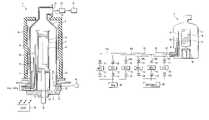
- FIG. 1is a structural view showing a vertical heat-processing apparatus according to a first embodiment of the present invention
- FIG. 2is a piping diagram mainly showing the gas supply section of the apparatus shown in FIG. 1 ;
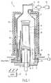
- FIG. 3is a structural view showing a vertical heat-processing apparatus according to a second embodiment of the present invention.
- FIG. 4is a graph showing the relationship of the film thickness of a silicon germanium film and planar uniformity thereof relative to wafer position, in a present example 1;
- FIG. 5is a graph showing the relationship of the germanium concentration in a silicon germanium film and planar uniformity thereof relative to wafer position, in the present example 1;
- FIG. 6is a graph showing the relationship of the film thickness of a silicon germanium film and planar uniformity thereof relative to wafer position, in a comparative example 1 and a comparative example 2;
- FIG. 7is a graph showing the relationship of the germanium concentration in a silicon germanium film and planar uniformity thereof relative to wafer position, in the comparative example 1 and comparative example 2;
- FIG. 8is a graph showing the relationship between the film-formation temperature for a silicon germanium film and electrically equivalent film thickness thereof.
- FIG. 9is a view showing a conventional vertical CVD apparatus for forming a silicon germanium film.
- the apparatus shown in FIG. 9needs to employ as many as four injectors ( 12 a to 12 d ) for mono-germane (five injectors 12 a to 12 d , and 13 , in total).
- injectors 12 a to 12 dfor mono-germane (five injectors 12 a to 12 d , and 13 , in total).
- the apparatus costincreases, and so does the space necessary for installing many gas supply devices.
- FIG. 1is a structural view showing a vertical heat-processing apparatus according to a first embodiment of the present invention.
- FIG. 2is a piping diagram mainly showing the gas supply section of the apparatus shown in FIG. 1 .
- the heat-processing apparatus (film-formation apparatus) 1includes a cylindrical reaction container 2 , which is made of, e.g., quartz and directed vertically.
- the reaction container 2is opened at the bottom to form a load port 21 , around which a flange 22 is integrally formed.
- a lid 3 made of, e.g., quartzis disposed below the reaction container 2 , so that the lid 3 can come into contact with the bottom of the flange 22 to airtightly close the port 21 .
- the lid 3is moved up and down by a boat elevator (not shown) to open and close the port.
- a rotary shaft 31extends through the center of the lid 3 , and supports a substrate holder or wafer boat 4 at the top.
- the wafer boat 4includes three or more, e.g. four, struts 41 .
- the struts 41have grooves (slots) to support a plurality of, e.g., 125, target substrates or semiconductor wafers W stacked at intervals.
- the 125 wafers Wconsist of dummy wafers disposed at the top and bottom sides, and product wafers placed therebetween.
- the bottom of the rotary shaft 31is connected to a motor 32 for rotating the rotary shaft 31 , so that the wafer boat 4 is rotated by the motor 32 .
- a heat-insulating unit 33is disposed on the lid 3 and surrounds the rotary shaft 31 .
- First to third injectors 51 to 53(constituting a common supply system) each having an L-shape are disposed equidistantly in the angular direction to extend through the flange 22 at the bottom of the reaction container 2 , and are used to supply process gases onto the wafers W within the reaction container 2 .
- the injectors 51 to 53have different lengths, such that the gas supply ports at their distal end (tip openings) are positioned at different heights.
- the distal end of the shortest first injector 51is positioned, e.g., near the bottom level of the range for holding wafers W in the wafer boat 4 .
- the distal end of the middle-length second injector 52is positioned, e.g., slightly below the central level of the range for holding wafers W in the wafer boat 4 .
- the distal end of the longest third injector 53is positioned, e.g., between the top level of the range for holding wafers W in the wafer boat 4 and the distal end of the second injector 52 .
- the layout of the injectors 51 to 53is not limited to that shown in FIG. 1 , and their lengths are suitably set based on experimental results or the like.
- the injectors 51 to 53are gathered in one area to be close to each other in the angular direction, so that maintenance can be easily performed.
- FIG. 1shows the injectors to penetrate the flange 22 at different heights, but they penetrate the flange 22 side by side in the horizontal direction.
- the proximal ends of the injectors 51 to 53are respectively connected to gas supply lines 61 to 63 , i.e., gas supply passages.
- the proximal end of the gas supply line 61is connected to gas supply lines 61 a and 61 b .
- the proximal end of the gas supply line 62is connected to gas supply lines 62 a and 62 b .
- the proximal end of the gas supply line 63is connected to gas supply lines 63 a and 63 b .
- the gas supply lines 61 a , 62 a , and 63 aare connected to a supply source 64 of a silane family gas, such as mono-silane gas.
- the gas supply lines 61 b , 62 b , and 63 bare connected to a supply source 65 of a germane family gas, such as mono-germane gas.
- a germane family gassuch as mono-germane gas.
- the mono-germane gasis a gas diluted to 10% by hydrogen gas.
- the gas supply lines 61 a , 62 a , and 63 a for supplying mono-silane gasare respectively provided with mass-flow controllers 71 to 73 used as flow rate regulators disposed thereon.
- the gas supply lines 61 b , 62 b , and 63 b for supplying mono-germane gasare respectively provided with mass-flow controllers 74 to 76 disposed thereon.
- the flow rates of mono-silane gas and mono-germane gascan be adjusted for each of the mixture gases supplied from the injectors 51 to 53 , independently of each other.
- Symbols V 1 to V 12denote valves.
- An exhaust port 23is formed at the top of the reaction container 2 to exhaust the interior of the reaction container 2 .
- the exhaust port 23is connected to an exhaust line 26 provided with a vacuum pump 25 and a pressure regulator 24 to vacuum-exhaust the interior of the reaction container 2 to a desired vacuum level.
- a furnace 35is disposed around the reaction container 2 , and includes a heater 34 for heating up the interior of the reaction container 2 .
- the heater 34is formed of a carbon wire heater, which allows a process to be performed with least contamination, i.e., at high cleanness, and allows temperature to be quickly increased and decreased.
- the film-formation apparatus 1includes a control section 20 formed of a computer.
- the control section 20is configured to activate a process program and read the description of a process recipe stored in a memory (not shown), so as to control the process conditions in accordance with the recipe.
- the control section 20outputs control signals to respectively control the heater 34 , pressure regulator 24 , and gas supply devices (such as valves, mass-flow controllers, etc.) of the gas supply section.
- a film-formation methodperformed in the film-formation apparatus 1 described above.
- a predetermined number of silicon wafers Ware placed and stacked at intervals on a wafer boat 4 , and the wafer boat 4 is then moved up by the boat elevator (not shown). With this operation, the wafer boat 4 is loaded into the reaction container 2 , and the bottom port of the flange 22 is closed by the lid 3 (the state shown in FIG. 1 ).
- the process field within the reaction container 2in which the wafer boat 4 is placed, is stabilized at a process temperature of, e.g., from 350 to 650° C.
- mono-silane gas and mono-germane gas respectively fed from the supply sources 64 and 65are mixed by the gas supply lines 61 to 63 and injectors 51 to 53 , which are used as mixing means.
- the mixture gasesare respectively supplied from the distal end supply ports of the injectors 51 to 53 , used as a common supply system, into the process field within the reaction container 2 .
- the interior of the reaction containeris vacuum-exhausted through the exhaust line 26 , and is adjusted to have a vacuum atmosphere of, e.g., from 10 to 130 Pa by the pressure regulator 24 .
- the injectors 51 to 53are given different mixture ratios between the process gases, i.e., mono-silane gas and mono-germane gas.
- the ratio of mono-silane gas relative to mono-germane gas in the mixture gas([mono-silane gas]/[mono-germane gas]) is set to be lower as the position of the supply ports of the injectors is higher.
- the mono-germane gas in this embodimentis a mono-germane gas diluted to 10% by hydrogen gas, as described above.
- the mono-silane gas and mono-germane gas thus suppliedreact with each other by thermal decomposition in the process field, and a silicon germanium film is thereby formed on the surface of the wafers W.
- the wafer boat 4is rotated by the motor 32 .
- supply of the process gasesis stopped, and the interior of the reaction container 2 is replaced with an inactive gas.
- the wafer boat 4is unloaded from the reaction container 2 , and is transferred to, e.g., an ion-implantation apparatus.
- a carrier impurity elementsuch as phosphorous (P) or boron (B) is implanted into the silicon germanium film.
- Pphosphorous
- Bboron
- the activation energy of mono-germaneis lower and thus the decomposition reactivity thereof is higher. If mono-germane is supplied solely from the bottom into the reaction container 2 , less mono-germane is present at the upper part of the wafer boat 4 .
- the apparatus shown in FIG. 1employs three injectors 51 to 53 with heights different from each other. As a consequence, mono-germane supplied from the injectors 52 and 53 compensates for a shortfall of mono-germane supplied from the lower injector 51 .
- mono-silane gas and mono-germane gasare mixed in advance, and supplied into the reaction container 2 thorough the injectors 51 to 53 .
- mono-germaneWhen mono-germane is supplied into the process field, it has been diluted by mono-silane, which has a higher activation energy and thus a lower decomposition reactivity. In this case, a decomposition reaction of mono-germane is suppressed by mono-silane.
- the number of injectorsis not limited to three, and it may be two, or four or more.
- the number of injectorsis set in accordance with the number of wafers W to be loaded (range for holding wafers W) or inter-substrate uniformity required.
- the structure of the first embodimentallows a high decomposition reactivity of mono-germane to be less influential, in terms of difference in film thickness and germanium concentration between upper and lower wafers. Specifically, if the same inter-substrate uniformity is to be attained, using the comparative structure and the structure of the first embodiment, the structure of the first embodiment requires a smaller number of injectors. In other words, the structure of the first embodiment requires a smaller number of gas line circuits, so the equipment cost and the installation space decrease.
- the process temperatureis the temperature of the process field within the reaction container 2 for accommodating the wafer boat 4 , and, more precisely, it is the set temperature at the center of an array of product wafers in the vertical direction.
- FIG. 3is a structural view showing a vertical heat-processing apparatus according to a second embodiment of the present invention.
- a plurality of injectors with different lengthsare disposed to supply the process gases (the mixture gas) into the process field from a plurality of positions along a direction in which wafers W are arrayed.
- a plurality of holes 81are formed as gas supply ports in a pipe 8 (distribution type injector) along the longitudinal direction thereof, wherein the pipe 8 extends in the vertical direction within the reaction container 2 , as shown in FIG. 3 .
- the holes (gas supply ports) 81are opened in the pipe 8 at positions facing the wafer boat 4 and between each two adjacent wafers W.
- the supply ports 81distribute a mixture gas of mono-silane gas and mono-germane gas into the process field.
- the hole size of the supply port 81may be gradually increased in accordance with its height (i.e., on the downstream side), so that the process gases can be uniformly supplied in the vertical direction.
- the silane family gasis not limited to mono-silane gas, and it may be a gas selected from the following materials: disilane (Si 2 H 6 ), dichloro silane (SiH 2 Cl 2 ), tetrachloro silane (SiCl 4 ), hexachloro silane (Si 2 Cl 6 ), hexaethylamino disilane, hexamethyl disilazane, disilylamine, trisilylamine, and bistertialbutylamino silane.
- a silicon germanium film obtained by the method described abovemay be a poly-silicon germanium film or amorphous silicon germanium film.
- Mono-germane gasmay be diluted or not diluted by hydrogen gas when used as mono-germane gas, as described above.
- the silicon germanium filmis supplied with a carrier impurity element by ion implantation to form a gate electrode.
- the silicon germanium filmmay be doped with phosphorous or boron by supplying a dopant gas, such as phosphine gas or boron trichloride, in film formation.
- a dopant gassuch as phosphine gas or boron trichloride
- the reaction container 2may be additionally provided with a dopant gas supply line or injector 55 , which is connected to a dopant gas supply circuit 56 . With this arrangement, a dopant gas is supplied from below the wafer boat 4 .
- a silicon germanium filmwas formed on the surface of silicon wafers W.
- the supply ports of injectors 51 to 53are set at heights corresponding to slot numbers “ 82 ”, “ 46 ”, and “ 20 ” of a wafer boat 4 .
- the slot numbersdenote slot positions of the wafer boat, in which a slot position is located on a lower side as its number symbol is higher.
- the process conditions for the silicon germanium filmwere set, as follows.
- the mono-germane gas usedwas a gas diluted to 10% by hydrogen gas.
- the wafers with a silicon germanium film formed thereonwere unloaded, and the thickness of the silicon germanium film and planar uniformity and inter-substrate uniformity thereof were measured. Further, the germanium concentration in the silicon germanium film and planar uniformity and inter-substrate uniformity thereof were measured.
- FIG. 4is a graph showing the relationship of the film thickness of a silicon germanium film and planar uniformity thereof relative to wafer position, in the present example 1.
- the horizontal axisdenotes numbers of slot positions of the wafer boat 4 , in which a slot position is located on a lower side as its number symbol is higher.
- the vertical axisdenotes the film thickness (nm) of a silicon germanium film and planar uniformity ( ⁇ %) of the film thickness.
- ⁇denotes a measurement of film thickness (the average value from nine points on the plane), and “ ⁇ ” denotes the planar uniformity thereof.
- FIG. 5is a graph showing the relationship of the germanium concentration in a silicon germanium film and planar uniformity thereof relative to wafer position, in the present example 1.
- the horizontal axisdenotes slot positions (slot numbers) of the wafer boat 4 .
- the vertical axisdenotes the germanium concentration (atm %) in a silicon germanium film and planar uniformity ( ⁇ %) thereof.
- ⁇denotes a measurement of germanium concentration in the film (the average value from five points on the plane), and “ ⁇ ” denotes the planar uniformity thereof.
- ⁇denotes a gas spouting position.
- the measured film thickness of the silicon germanium film on the wafers Wwas within a range of from 70 to 75 nm.
- the planar uniformity of the film thicknesswas within a range of from ⁇ 1.5% to ⁇ 3%, and the inter-substrate uniformity of the film thickness was ⁇ 1.27%.
- Tmaxis the maximum value among measurement points
- Tminis the minimum value among measurement points
- Xis the average value of measured values (of the film thickness or concentration).
- Kmaxis the maximum value among the average values of the film thickness or concentration on all the monitor wafers
- Kminis the minimum value among the average values of the film thickness or concentration on all the monitor wafers
- Yis the average value from all the wafers in terms of the average values on the respective wafers.
- the measured germanium concentration in the silicon germanium film on the wafers Wwas within a range of from 21 to 23 atm %.
- the planar uniformity of the germanium concentrationwas within a range of from ⁇ 1% to ⁇ 2%, and the inter-substrate uniformity of the germanium concentration was ⁇ 2.18%.
- a silicon germanium filmwas formed in the same manner as the present example 1, except that only one injector was disposed in the reaction container 2 .
- the supply port of the injectorwas set at a height slightly lower than the lowest level (slot number 125 ) of the wafer boat 4 . Under these conditions, wafers W were subjected to the film-formation process in the comparative example 1.
- a silicon germanium filmwas formed on wafers W in the same manner as the present example 1, except that two injectors having supply ports at the same height were disposed in the reaction container 2 , and used to separately supply mono-silane gas and mono-germane gas into the process field.
- the film thickness of the silicon germanium film and planar uniformity and inter-substrate uniformity thereofwere measured. Further, the germanium concentration in the silicon germanium film and planar uniformity and inter-substrate uniformity thereof were measured.
- FIG. 6is a graph showing the relationship of the film thickness of a silicon germanium film and planar uniformity thereof relative to wafer position, in the comparative example 1 (CE1) and comparative example (CE2).
- the horizontal axisdenotes slot positions (slot numbers) of the wafer boat 4 .
- the vertical axisdenotes the film thickness (nm) of a silicon germanium film and planar uniformity ( ⁇ %) of the film thickness.
- “ ⁇ ” and “x”denote a film thickness (the average value from nine points on the plane) on the comparative examples 1 and 2, respectively
- ⁇ ” and “ ⁇ ”denote the planar uniformity of the film thickness on the comparative examples 1 and 2, respectively.
- FIG. 7is a graph showing the relationship of the germanium concentration in a silicon germanium film and planar uniformity thereof relative to wafer position, in the comparative example 1 (CE1) and comparative example (CE2).
- the horizontal axisdenotes slot positions (slot numbers) of the wafer boat 4 .
- the vertical axisdenotes the germanium concentration (atm %) in a silicon germanium film and planar uniformity ( ⁇ %) thereof.
- “ ⁇ ” and “x”denote a germanium concentration (the average value from five points on the plane) in the comparative examples 1 and 2, respectively
- “ ⁇ ” and “ ⁇ ”denote the planar uniformity of the germanium concentration in the comparative examples 1 and 2, respectively.
- the measured film thickness of the silicon germanium on the wafers Wwas within a range of from 40 to 55 nm in the comparative example 1 (CE1), and it was within a range of from 40 to 60 nm in the comparative example 2 (CE2).
- the planar uniformity of the film thicknesswas within a range of from +1.2% to ⁇ 2% in the comparative example 1, and it was within a range of from ⁇ 1.2% to ⁇ 1.5% in the comparative example 2.
- the inter-substrate uniformity of the film thicknesswas +10.34% in the comparative example 1, and it was ⁇ 19.89% in the comparative example 2.
- the measured germanium concentration in the silicon germanium on the wafers Wwas within a range of from 15 to 18 atm % in the comparative example 1 (CE1), and it was within a range of from 15 to 22 atm % in the comparative example 2 (CE2).
- the planar uniformity of the germanium concentrationwas within a range of from +0.5% to +10 in the comparative example 1, and it was within a range of from ⁇ 0.5% to ⁇ 2% in the comparative example 2.
- the inter-substrate uniformity of the germanium concentrationwas ⁇ 7.746 in the comparative example 1, and it was ⁇ 15.14% in the comparative example 2.
- the comparative example 1was slightly better in the planar uniformity of the film thickness and germanium concentration, but it was remarkably worse in the inter-substrate uniformity thereof. Since the present example 1 was far better in the inter-substrate uniformity, it has been confirmed that disposing a plurality of injectors to compensate for a shortfall of gas from the upstream side is effective.
- the comparative example 2in which mono-germane gas and mono-silane gas were separately supplied into the reaction container 2 , was worse in the planar uniformity. This was so because the film thickness and germanium concentration were locally very high on the upstream side (near the bottom of the wafer boat 4 ).
- mono-germane gas supplied from an injectoris less diluted, immediately after it is supplied, by mono-silane gas supplied from another injector, and thus the consumption amount of mono-germane is high.
- the mono-germane gasflows upward, it is mixed with the mono-silane gas and the consumption amount is stabilized. It is thought that this mechanism brought about the result shown in FIG. 6 . Accordingly, it has been confirmed that supplying a mixture of mono-germane gas and mono-silane gas is highly advantageous.
- a gate insulating filmwas formed to be 3 mm on a silicon substrate, and a silicon germanium film was then formed in the same manner as the present example 1, except that the process temperature was set at 510° C., 550° C., or 620° C. Then, the electrically equivalent film thickness of the silicon germanium film was determined.
- FIG. 8is a graph showing the relationship between the film-formation temperature for a silicon germanium film and electrically equivalent film thickness thereof.
- FIG. 8also shows the electrically equivalent film thickness of a poly-silicon film. As shown in FIG. 8 , with increase in the film-formation temperature, the electrically equivalent film thickness became smaller. A smaller value of the electrically equivalent film thickness means that depletion of a gate can be more suppressed when a transistor is turned on.
- the film-formation temperature for silicon germaniumis preferably set at, e.g., 350° C. or more. Accordingly, for the film quality of a transistor, a higher temperature is preferably used. Accordingly to the first and second embodiments, even where the film-formation temperature is higher and decomposition of mono-germane is accelerated, a high inter-substrate uniformity in the film thickness and germanium concentration can be maintained. As a consequence, the embodiments are very effective techniques for use in manufacturing semiconductor devices that employ silicon germanium.
Landscapes
- Chemical & Material Sciences (AREA)
- General Chemical & Material Sciences (AREA)
- Chemical Kinetics & Catalysis (AREA)
- Engineering & Computer Science (AREA)
- Materials Engineering (AREA)
- Mechanical Engineering (AREA)
- Metallurgy (AREA)
- Organic Chemistry (AREA)
- Inorganic Chemistry (AREA)
- Chemical Vapour Deposition (AREA)
- Electrodes Of Semiconductors (AREA)
Abstract
Description
The present application is a Divisional application of U.S. Ser. No. 10/965,789, filed Oct. 18, 2004, and is based upon and claims the benefit of priority from prior Japanese Patent Application No. 2003-359634, filed Oct. 20, 2003, the entire contents of which are incorporated herein by reference.
1. Field of the Invention
The present invention relates to a vertical CVD apparatus and CVD method for processing a plurality of target substrates all together to form a silicon germanium film, and particularly relates to a technique used for semiconductor processes. The term “semiconductor process” used herein includes various kinds of processes which are performed to manufacture a semiconductor device or a structure having wiring layers, electrodes, and the like to be connected to a semiconductor device, on a target substrate, such as a semiconductor wafer or a glass substrate used for an LCD (Liquid Crystal Display) or FPD (Flat Panel Display), by forming semiconductor layers, insulating layers, and conductive layers in predetermined patterns on the target substrate.
2. Description of the Related Art
Conventionally, for example, poly-silicon is used for gate electrodes of transistors. Gate electrodes of poly-silicon can be easily depleted, when supplied with a bias voltage. As the thickness of gate insulating films decreases, this becomes prominent, which is one of the causes of device properties being deteriorated. In order to solve this problem, it has been studied to employ silicon germanium, which has a higher dopant activation rate, in place of silicon. For example, Jpn. Pat. Appln. KOKAI Publication No. 2003-77845 (patent publication 1: see FIG. 1 and Paragraph 17) discloses a method for forming a silicon germanium film on the surface of a semiconductor wafer. This method employs a vertical heat-processing apparatus, which supplies mono-silane (SiH4) gas and mono-germane (GeH4) gas to form a silicon germanium film by CVD.
Fourinjectors 12ato12dwith different lengths for supplying mono-germane are disposed beside thewafer boat 17 in thereaction container 11. Aninjector 13 is disposed at the bottom of theinner tube 15 for supplying a mixture gas prepared by mixing mono-silane and mono-germane. It should be noted that the patent publication 1 includes an error inFIG. 1 , concerning theinjectors 12ato12d.
The source gases supplied from theinjectors 12ato12dand13 flow upward within theinner tube 15, and then enter the gap between theinner tube 15 andouter tube 14 from the top and exhausted from the bottom. As compared to mono-silane and mono-germane with each other in decomposition reactivity, mono-germane is higher than mono-silane in decomposition reactivity, so mono-germane is consumed more. Accordingly, if only theinjector 13 is used, the wafers end up having larger values in the thickness of a silicon germanium film and germanium concentration, as the position of the wafers is closer to the supply port of theinjector 13. For this reason, this apparatus employs the fourinjectors 12ato12dwith different heights for supplying mono-germane to compensate for a shortfall of germanium on the downstream side.
An object of the present invention is to provide a vertical CVD apparatus and CVD method, which allows a silicon germanium film formed to have high inter-substrate uniformity in the film thickness and germanium concentration.
According to a first aspect of the present invention, there is provided a vertical CVD apparatus for processing a plurality of target substrates all together to form a silicon germanium film, the apparatus comprising:
a reaction container having a process field configured to accommodate the target substrates;
a holder configured to hold the target substrates stacked at intervals within the reaction container;
a heater configured to heat the process field;
an exhaust system configured to exhaust the reaction container;
a common supply system including a plurality of supply ports disposed at different heights and configured to supply a mixture gas into the process field, the mixture gas comprising a first process gas of a silane family and a second process gas of a germane family;
a first gas supply circuit configured to supply the first process gas into the common supply system; and
a second gas supply circuit configured to supply the second process gas into the common supply system.
According to a second aspect of the present invention, there is provided a vertical CVD method for processing a plurality of target substrates all together to form a silicon germanium film, the method comprising:
placing a holder in a process field within a reaction container, the holder holding the target substrates stacked at intervals; and
forming a silicon germanium film by CVD on the target substrates within the process field, while setting the process field at a first temperature and a first pressure, and supplying a mixture gas into the process field through a plurality of supply ports disposed at different heights, the mixture gas comprising a first process gas of a silane family and a second process gas of a germane family.
Additional objects and advantages of the invention will be set forth in the description which follows, and in part will be obvious from the description, or may be learned by practice of the invention. The objects and advantages of the invention may be realized and obtained by means of the instrumentalities and combinations particularly pointed out hereinafter.
The accompanying drawings, which are incorporated in and constitute a part of the specification, illustrate embodiments of the invention, and together with the general description given above and the detailed description of the embodiments given below, serve to explain the principles of the invention.
In the process of developing the present invention, the inventors studied problems related to the conventional vertical CVD apparatus for forming a silicon germanium film shown inFIG. 9 (disclosed in the patent publication 1). As a result, the inventors have arrived at the findings given below.
According to the apparatus shown inFIG. 9 , looking at two gas supply ports vertically adjacent to each other, mono-germane flowing out of the lower supply port is immediately decomposed at a higher decomposition rate, and thus a wafer closer to the lower supply port consumes a larger amount of mono-germane. As a consequent, the upper and lower wafers differ from each other in film thickness and germanium concentration, resulting in lower inter-substrate uniformity (between wafers).
In order to improve inter-wafer uniformity to attain a high yield, the intervals of supply ports have to be smaller, as the thickness of films used in semiconductor devices decreases. Accordingly, the apparatus shown inFIG. 9 needs to employ as many as four injectors (12ato12d) for mono-germane (fiveinjectors 12ato12d, and13, in total). In this case, with increase in the number of injectors, it is necessary to also respectively increase the number of supply devices for supplying process gases and mass-flow controllers for controlling gas flow rates, by that much. As a consequence, the apparatus cost increases, and so does the space necessary for installing many gas supply devices.
Embodiments of the present invention achieved on the basis of the findings given above will now be described with reference to the accompanying drawings. In the following description, the constituent elements having substantially the same function and arrangement are denoted by the same reference numerals, and a repetitive description will be made only when necessary.
Thewafer boat 4 includes three or more, e.g. four, struts41. Thestruts 41 have grooves (slots) to support a plurality of, e.g., 125, target substrates or semiconductor wafers W stacked at intervals. The 125 wafers W consist of dummy wafers disposed at the top and bottom sides, and product wafers placed therebetween. The bottom of therotary shaft 31 is connected to amotor 32 for rotating therotary shaft 31, so that thewafer boat 4 is rotated by themotor 32. A heat-insulatingunit 33 is disposed on thelid 3 and surrounds therotary shaft 31.
First tothird injectors 51 to53 (constituting a common supply system) each having an L-shape are disposed equidistantly in the angular direction to extend through theflange 22 at the bottom of thereaction container 2, and are used to supply process gases onto the wafers W within thereaction container 2. Theinjectors 51 to53 have different lengths, such that the gas supply ports at their distal end (tip openings) are positioned at different heights. The distal end of the shortestfirst injector 51 is positioned, e.g., near the bottom level of the range for holding wafers W in thewafer boat 4. The distal end of the middle-lengthsecond injector 52 is positioned, e.g., slightly below the central level of the range for holding wafers W in thewafer boat 4. The distal end of the longestthird injector 53 is positioned, e.g., between the top level of the range for holding wafers W in thewafer boat 4 and the distal end of thesecond injector 52. The layout of theinjectors 51 to53 is not limited to that shown inFIG. 1 , and their lengths are suitably set based on experimental results or the like. Theinjectors 51 to53 are gathered in one area to be close to each other in the angular direction, so that maintenance can be easily performed.FIG. 1 shows the injectors to penetrate theflange 22 at different heights, but they penetrate theflange 22 side by side in the horizontal direction.
As shown inFIG. 2 , the proximal ends of theinjectors 51 to53 are respectively connected togas supply lines 61 to63, i.e., gas supply passages. The proximal end of thegas supply line 61 is connected togas supply lines gas supply line 62 is connected togas supply lines gas supply line 63 is connected togas supply lines gas supply lines supply source 64 of a silane family gas, such as mono-silane gas. Thegas supply lines supply source 65 of a germane family gas, such as mono-germane gas. In this embodiment, the mono-germane gas is a gas diluted to 10% by hydrogen gas.
Thegas supply lines flow controllers 71 to73 used as flow rate regulators disposed thereon. Thegas supply lines flow controllers 74 to76 disposed thereon. The flow rates of mono-silane gas and mono-germane gas can be adjusted for each of the mixture gases supplied from theinjectors 51 to53, independently of each other. Symbols V1 to V12 denote valves.
Anexhaust port 23 is formed at the top of thereaction container 2 to exhaust the interior of thereaction container 2. Theexhaust port 23 is connected to anexhaust line 26 provided with avacuum pump 25 and apressure regulator 24 to vacuum-exhaust the interior of thereaction container 2 to a desired vacuum level. Afurnace 35 is disposed around thereaction container 2, and includes aheater 34 for heating up the interior of thereaction container 2. Theheater 34 is formed of a carbon wire heater, which allows a process to be performed with least contamination, i.e., at high cleanness, and allows temperature to be quickly increased and decreased.
Further, the film-formation apparatus1 includes acontrol section 20 formed of a computer. Thecontrol section 20 is configured to activate a process program and read the description of a process recipe stored in a memory (not shown), so as to control the process conditions in accordance with the recipe. Thecontrol section 20 outputs control signals to respectively control theheater 34,pressure regulator 24, and gas supply devices (such as valves, mass-flow controllers, etc.) of the gas supply section.
Next, an explanation will be given of a film-formation method, performed in the film-formation apparatus1 described above. First, a predetermined number of silicon wafers W are placed and stacked at intervals on awafer boat 4, and thewafer boat 4 is then moved up by the boat elevator (not shown). With this operation, thewafer boat 4 is loaded into thereaction container 2, and the bottom port of theflange 22 is closed by the lid3 (the state shown inFIG. 1 ).
Then, the process field within thereaction container 2, in which thewafer boat 4 is placed, is stabilized at a process temperature of, e.g., from 350 to 650° C. Then, mono-silane gas and mono-germane gas respectively fed from thesupply sources gas supply lines 61 to63 andinjectors 51 to53, which are used as mixing means. Then, the mixture gases are respectively supplied from the distal end supply ports of theinjectors 51 to53, used as a common supply system, into the process field within thereaction container 2. Also, the interior of the reaction container is vacuum-exhausted through theexhaust line 26, and is adjusted to have a vacuum atmosphere of, e.g., from 10 to 130 Pa by thepressure regulator 24.
Theinjectors 51 to53 are given different mixture ratios between the process gases, i.e., mono-silane gas and mono-germane gas. The mixture ratio at theinjector 51 is set to be [mono-silane gas]/[mono-germane gas]=1200 sccm/600 sccm. The mixture ratio at theinjector 52 is set to be [mono-silane gas]/[mono-germane gas]=300 sccm/190 sccm. The mixture ratio at theinjector 53 is set to be [mono-silane gas]/[mono-germane gas]=300 sccm/220 sccm. In other words, according to this embodiment, the ratio of mono-silane gas relative to mono-germane gas in the mixture gas ([mono-silane gas]/[mono-germane gas]) is set to be lower as the position of the supply ports of the injectors is higher. It should be noted that, the mono-germane gas in this embodiment is a mono-germane gas diluted to 10% by hydrogen gas, as described above.
The mono-silane gas and mono-germane gas thus supplied react with each other by thermal decomposition in the process field, and a silicon germanium film is thereby formed on the surface of the wafers W. At this time, thewafer boat 4 is rotated by themotor 32. After the film-formation process is performed for a predetermined time, supply of the process gases is stopped, and the interior of thereaction container 2 is replaced with an inactive gas.
Then, thewafer boat 4 is unloaded from thereaction container 2, and is transferred to, e.g., an ion-implantation apparatus. A carrier impurity element, such as phosphorous (P) or boron (B), is implanted into the silicon germanium film. By doing so, a structure is formed in which the silicon germanium film is employed as a gate electrode.
According to the first embodiment, the following advantages can be obtained. Specifically, the activation energy of mono-germane is lower and thus the decomposition reactivity thereof is higher. If mono-germane is supplied solely from the bottom into thereaction container 2, less mono-germane is present at the upper part of thewafer boat 4. In this respect, the apparatus shown inFIG. 1 employs threeinjectors 51 to53 with heights different from each other. As a consequence, mono-germane supplied from theinjectors lower injector 51.
Rather than being separately supplied from each other, mono-silane gas and mono-germane gas are mixed in advance, and supplied into thereaction container 2 thorough theinjectors 51 to53. When mono-germane is supplied into the process field, it has been diluted by mono-silane, which has a higher activation energy and thus a lower decomposition reactivity. In this case, a decomposition reaction of mono-germane is suppressed by mono-silane.
Looking at the respective parts between the distal end supply ports of theinjectors 51 to53, mono-germane in the mixture gas spouted from the supply port of the lower injector (51 or52) is decomposed and consumed while it flows to the upper injector (52 or53). However, since the decomposition reactivity of mono-germane is suppressed, although the lower wafer W still consumes mono-germane more than the upper wafer W does, the difference in consumption amount of mono-germane between lower and upper wafers W becomes smaller. As consequence, it is possible to attain high inter-substrate (between wafers W) uniformity in the film thickness of a silicon germanium film and germanium concentration, thereby improving the yield.
The number of injectors is not limited to three, and it may be two, or four or more. The number of injectors is set in accordance with the number of wafers W to be loaded (range for holding wafers W) or inter-substrate uniformity required.
As a comparative structure, there may be a structure in which mono-silane gas and mono-germane gas are separately supplied into a process field, wherein the mono-silane gas is from the bottom of thereaction container 2, and the mono-germane gas is from a plurality of injectors. As compared to this comparative structure, the structure of the first embodiment allows a high decomposition reactivity of mono-germane to be less influential, in terms of difference in film thickness and germanium concentration between upper and lower wafers. Specifically, if the same inter-substrate uniformity is to be attained, using the comparative structure and the structure of the first embodiment, the structure of the first embodiment requires a smaller number of injectors. In other words, the structure of the first embodiment requires a smaller number of gas line circuits, so the equipment cost and the installation space decrease.
As shown inFIG. 8 described later, the properties of a silicon germanium film improve with higher process temperatures. However, since the decomposition reactivity of mono-germane also increases, as a consequence of the increased the process temperature, the process temperature should not be greatly increased, in practice. In the first embodiment, since mono-germane is diluted with mono-silane, the inter-substrate uniformity remains satisfactory, even where the process temperature is set at 350° C. or more, e.g., 540° C. In recent years, there is a tendency to use a higher process temperature, a larger wafer size, and a larger batch of wafers to be processed; for which the first embodiment is very effective. It should be noted that the process temperature is the temperature of the process field within thereaction container 2 for accommodating thewafer boat 4, and, more precisely, it is the set temperature at the center of an array of product wafers in the vertical direction.
In the first and second embodiments, the silane family gas is not limited to mono-silane gas, and it may be a gas selected from the following materials: disilane (Si2H6), dichloro silane (SiH2Cl2), tetrachloro silane (SiCl4), hexachloro silane (Si2Cl6), hexaethylamino disilane, hexamethyl disilazane, disilylamine, trisilylamine, and bistertialbutylamino silane. A silicon germanium film obtained by the method described above may be a poly-silicon germanium film or amorphous silicon germanium film. Mono-germane gas may be diluted or not diluted by hydrogen gas when used as mono-germane gas, as described above.
In the first embodiment, the silicon germanium film is supplied with a carrier impurity element by ion implantation to form a gate electrode. Alternatively, the silicon germanium film may be doped with phosphorous or boron by supplying a dopant gas, such as phosphine gas or boron trichloride, in film formation. In this case, as shown with a phantom line inFIG. 1 , thereaction container 2 may be additionally provided with a dopant gas supply line orinjector 55, which is connected to a dopantgas supply circuit 56. With this arrangement, a dopant gas is supplied from below thewafer boat 4.
Using the film-formation apparatus1 shown inFIG. 1 , a silicon germanium film was formed on the surface of silicon wafers W. The supply ports ofinjectors 51 to53 are set at heights corresponding to slot numbers “82”, “46”, and “20” of awafer boat 4. The slot numbers denote slot positions of the wafer boat, in which a slot position is located on a lower side as its number symbol is higher. The process conditions for the silicon germanium film were set, as follows.
Set temperature: 540° C.
Set pressure: 47 Pa.
Flow rate ratios ([mono-silane gas]/[mono-germane gas]) at the injectors:
- First injector51: 1200 sccm/600 sccm,
- Second injector52: 300 sccm/190 sccm,
- Third injector53: 300 sccm/200 sccm.
The mono-germane gas used was a gas diluted to 10% by hydrogen gas.
In the present example 1, the wafers with a silicon germanium film formed thereon were unloaded, and the thickness of the silicon germanium film and planar uniformity and inter-substrate uniformity thereof were measured. Further, the germanium concentration in the silicon germanium film and planar uniformity and inter-substrate uniformity thereof were measured.
As shown inFIG. 4 , the measured film thickness of the silicon germanium film on the wafers W was within a range of from 70 to 75 nm. The planar uniformity of the film thickness was within a range of from ±1.5% to ±3%, and the inter-substrate uniformity of the film thickness was ±1.27%. The planar uniformity and inter-substrate uniformity are expressed by the following formulas.
Planar uniformity={(Tmax−Tmin)/2X}×100(%)
Planar uniformity={(Tmax−Tmin)/2X}×100(%)
Where Tmax is the maximum value among measurement points, Tmin is the minimum value among measurement points, and X is the average value of measured values (of the film thickness or concentration).
Inter-substrate uniformity={(Kmax−Kmin)/2Y}×100(%)
Inter-substrate uniformity={(Kmax−Kmin)/2Y}×100(%)
Where Kmax is the maximum value among the average values of the film thickness or concentration on all the monitor wafers, Kmin is the minimum value among the average values of the film thickness or concentration on all the monitor wafers, and Y is the average value from all the wafers in terms of the average values on the respective wafers.
As shown inFIG. 5 , the measured germanium concentration in the silicon germanium film on the wafers W was within a range of from 21 to 23 atm %. The planar uniformity of the germanium concentration was within a range of from ±1% to ±2%, and the inter-substrate uniformity of the germanium concentration was ±2.18%.
A silicon germanium film was formed in the same manner as the present example 1, except that only one injector was disposed in thereaction container 2. The supply port of the injector was set at a height slightly lower than the lowest level (slot number125) of thewafer boat 4. Under these conditions, wafers W were subjected to the film-formation process in the comparative example 1.
A silicon germanium film was formed on wafers W in the same manner as the present example 1, except that two injectors having supply ports at the same height were disposed in thereaction container 2, and used to separately supply mono-silane gas and mono-germane gas into the process field.
Then, for the wafers according to the comparative examples 1 and 2, the film thickness of the silicon germanium film and planar uniformity and inter-substrate uniformity thereof were measured. Further, the germanium concentration in the silicon germanium film and planar uniformity and inter-substrate uniformity thereof were measured.
As shown inFIG. 6 , the measured film thickness of the silicon germanium on the wafers W was within a range of from 40 to 55 nm in the comparative example 1 (CE1), and it was within a range of from 40 to 60 nm in the comparative example 2 (CE2). The planar uniformity of the film thickness was within a range of from +1.2% to ±2% in the comparative example 1, and it was within a range of from ±1.2% to ±1.5% in the comparative example 2. The inter-substrate uniformity of the film thickness was +10.34% in the comparative example 1, and it was ±19.89% in the comparative example 2.
As shown inFIG. 7 , the measured germanium concentration in the silicon germanium on the wafers W was within a range of from 15 to 18 atm % in the comparative example 1 (CE1), and it was within a range of from 15 to 22 atm % in the comparative example 2 (CE2). The planar uniformity of the germanium concentration was within a range of from +0.5% to +10 in the comparative example 1, and it was within a range of from ±0.5% to ±2% in the comparative example 2. The inter-substrate uniformity of the germanium concentration was ±7.746 in the comparative example 1, and it was ±15.14% in the comparative example 2.
As compared to the present example 1, the comparative example 1 was slightly better in the planar uniformity of the film thickness and germanium concentration, but it was remarkably worse in the inter-substrate uniformity thereof. Since the present example 1 was far better in the inter-substrate uniformity, it has been confirmed that disposing a plurality of injectors to compensate for a shortfall of gas from the upstream side is effective.
As compared to the comparative example 1, the comparative example 2, in which mono-germane gas and mono-silane gas were separately supplied into thereaction container 2, was worse in the planar uniformity. This was so because the film thickness and germanium concentration were locally very high on the upstream side (near the bottom of the wafer boat4). Specifically, where mono-germane gas is separately supplied into the process field, mono-germane gas supplied from an injector is less diluted, immediately after it is supplied, by mono-silane gas supplied from another injector, and thus the consumption amount of mono-germane is high. As the mono-germane gas flows upward, it is mixed with the mono-silane gas and the consumption amount is stabilized. It is thought that this mechanism brought about the result shown inFIG. 6 . Accordingly, it has been confirmed that supplying a mixture of mono-germane gas and mono-silane gas is highly advantageous.
A gate insulating film was formed to be 3 mm on a silicon substrate, and a silicon germanium film was then formed in the same manner as the present example 1, except that the process temperature was set at 510° C., 550° C., or 620° C. Then, the electrically equivalent film thickness of the silicon germanium film was determined.
As described above, the film-formation temperature for silicon germanium is preferably set at, e.g., 350° C. or more. Accordingly, for the film quality of a transistor, a higher temperature is preferably used. Accordingly to the first and second embodiments, even where the film-formation temperature is higher and decomposition of mono-germane is accelerated, a high inter-substrate uniformity in the film thickness and germanium concentration can be maintained. As a consequence, the embodiments are very effective techniques for use in manufacturing semiconductor devices that employ silicon germanium.
Additional advantages and modifications will readily occur to those skilled in the art. Therefore, the invention in its broader aspects is not limited to the specific details and representative embodiments shown and described herein. Accordingly, various modifications may be made without departing from the spirit or scope of the general inventive concept as defined by the appended claims and their equivalents.
Claims (14)
1. A vertical CVD method for processing a plurality of target substrates all together to form a silicon germanium film, the method comprising:
placing a holder in a process field within a reaction container, the holder holding the target substrates stacked at intervals; and
forming a silicon germanium film by CVD on the target substrates within the process field, while setting the process field at a first temperature and a first pressure, and supplying a first process gas of a silane family and a second process gas of a germane family into the process field,
wherein said forming a silicon germanium film comprises
preparing a plurality of mixture gases with different ratios of the first process gas relative to the second process gas by mixing the first and second process gases,
supplying the plurality of mixture gases into the process field respectively through a plurality of supply ports disposed at different heights inside the reaction container such that the ratios of the plurality of mixture gases are lower as the supply ports are high in position, and
exhausting gas upward from the process field.
2. The method according toclaim 1 , wherein said forming a silicon germanium film is arranged such that the first temperature is set to be within a range of from 350 to 650° C. and the first pressure is set to be within a range of from 10 to 130 Pa.
3. The method according toclaim 1 , wherein said exhausting gas upward from the process field is performed by use of an exhaust port disposed at a top of the reaction container.
4. The method according toclaim 1 , wherein said forming a silicon germanium film further comprises supplying a dopant gas into the process field, the dopant gas being used for doping the silicon germanium film with a carrier impurity.
5. The method according toclaim 1 , wherein the first process gas is mono-silane (SiH4) gas and the second process gas is mono-germane (GeH4) gas.
6. The method according toclaim 1 , wherein the plurality of supply ports comprise first, second, and third supply ports such that the second supply port is located above the first supply port and the third supply port is located above the second supply port,
the plurality of mixture gases comprise first, second, and third mixture gases respectively with first, second, and third ratios of the first process gas relative to the second process gas such that the second ratio is lower than the first ratio and the third ratio is lower than the second ratio, and
said forming a silicon germanium film is arranged to supply first, second, and third mixture gases respectively through the first, second, and third supply ports.
7. A vertical CVD method for processing a plurality of target substrates all together to form a silicon germanium film in a vertical CVD apparatus,
the apparatus comprising:
a reaction container having a process field configured to accommodate the target substrates;
a holder configured to hold the target substrates stacked at intervals within the reaction container;
a heater configured to heat the process field;
an exhaust system configured to exhaust the reaction container such that gas flows upward inside the process field;
a gas supply system configured to supply a first process gas of a silane family and a second process gas of a germane family into the process field, the gas supply system including a plurality of supply ports disposed at different heights inside the reaction container; and
a control section configured to control an operation of the apparatus,
the method comprising:
placing the holder in the process field within the reaction container, the holder holding the target substrates stacked at intervals; and
forming a silicon germanium film by CVD on the target substrates within the process field, while setting the process field at a first temperature and a first pressure, and supplying the first and second process gases into the process field,
wherein said forming a silicon germanium film is performed under control of the control section and comprises
preparing a plurality of mixture gases with different ratios of the first process gas relative to the second process gas by mixing the first and second process gases,
supplying the plurality of mixture gases into the process field respectively through the plurality of supply ports such that the ratios of the plurality of mixture gases are lower as the supply ports are higher in position, and
exhausting gas upward from the process field.
8. The method according toclaim 7 , wherein the gas supply system comprises a plurality of injectors inserted into the reaction container and respectively having the plurality of supply ports.
9. The method according toclaim 8 , wherein the gas supply system comprises a first gas supply circuit configured to supply the first process gas and including branch lines respectively connected to the plurality of injectors, and a second gas supply circuit configured to supply the second process gas and including branch lines respectively connected to the plurality of injectors, the branch lines of the first and second supply circuits being respectively provided with flow rate regulators, and
said forming a silicon germanium film comprises adjusting the flow rate regulators to set the ratios of the plurality of mixture gases under control of the control section.
10. The method according toclaim 7 , wherein said forming a silicon germanium film is arranged such that the first temperature is set to be within a range of from 350 to 650° C. and the first pressure is set to be within a range of from 10 to 130 Pa.
11. The method according toclaim 7 , wherein said exhausting gas upward from the process field is performed by use of an exhaust port disposed at a top of the reaction container.
12. The method according toclaim 7 , wherein said forming a silicon germanium film further comprises supplying a dopant gas into the process field, the dopant gas being used for doping the silicon germanium film with a carrier impurity.
13. The method according toclaim 7 , wherein the first process gas is a mono-silane (SiH4) gas and the second process gas is mono-germane (GeH4) gas.
14. The method according toclaim 7 , wherein the plurality of supply ports comprise first, second, and third supply ports such that the second supply port is located above the first supply port and the third supply port is located above the second supply port,
the plurality of mixture gases comprise first, second, and third mixture gases respectively with first, second, and third ratios of the first process gas relative to the second process gas such that the second ratio is lower than the first ratio and the third ratio is lower than the second ratio, and
said forming a silicon germanium film is arranged to supply first, second, and third mixture gases respectively through the first, second, and third supply ports.
Priority Applications (1)
| Application Number | Priority Date | Filing Date | Title |
|---|---|---|---|
| US12/341,642US7648895B2 (en) | 2003-10-20 | 2008-12-22 | Vertical CVD apparatus for forming silicon-germanium film |
Applications Claiming Priority (4)
| Application Number | Priority Date | Filing Date | Title |
|---|---|---|---|
| JP2003359634AJP2005123532A (en) | 2003-10-20 | 2003-10-20 | Deposition system and deposition method |
| JP2003-359634 | 2003-10-20 | ||
| US10/965,789US20050181586A1 (en) | 2003-10-20 | 2004-10-18 | Vertical CVD apparatus for forming silicon-germanium film |
| US12/341,642US7648895B2 (en) | 2003-10-20 | 2008-12-22 | Vertical CVD apparatus for forming silicon-germanium film |
Related Parent Applications (1)
| Application Number | Title | Priority Date | Filing Date |
|---|---|---|---|
| US10/965,789DivisionUS20050181586A1 (en) | 2003-10-20 | 2004-10-18 | Vertical CVD apparatus for forming silicon-germanium film |
Publications (2)
| Publication Number | Publication Date |
|---|---|
| US20090104760A1 US20090104760A1 (en) | 2009-04-23 |
| US7648895B2true US7648895B2 (en) | 2010-01-19 |
Family
ID=34615795
Family Applications (2)
| Application Number | Title | Priority Date | Filing Date |
|---|---|---|---|
| US10/965,789AbandonedUS20050181586A1 (en) | 2003-10-20 | 2004-10-18 | Vertical CVD apparatus for forming silicon-germanium film |
| US12/341,642Expired - Fee RelatedUS7648895B2 (en) | 2003-10-20 | 2008-12-22 | Vertical CVD apparatus for forming silicon-germanium film |
Family Applications Before (1)
| Application Number | Title | Priority Date | Filing Date |
|---|---|---|---|
| US10/965,789AbandonedUS20050181586A1 (en) | 2003-10-20 | 2004-10-18 | Vertical CVD apparatus for forming silicon-germanium film |
Country Status (4)
| Country | Link |
|---|---|
| US (2) | US20050181586A1 (en) |
| JP (1) | JP2005123532A (en) |
| KR (1) | KR100907148B1 (en) |
| TW (1) | TW200527518A (en) |
Cited By (273)
| Publication number | Priority date | Publication date | Assignee | Title |
|---|---|---|---|---|
| US11004977B2 (en) | 2017-07-19 | 2021-05-11 | Asm Ip Holding B.V. | Method for depositing a group IV semiconductor and related semiconductor device structures |
| US11001925B2 (en) | 2016-12-19 | 2021-05-11 | Asm Ip Holding B.V. | Substrate processing apparatus |
| US11018002B2 (en) | 2017-07-19 | 2021-05-25 | Asm Ip Holding B.V. | Method for selectively depositing a Group IV semiconductor and related semiconductor device structures |
| US11015245B2 (en) | 2014-03-19 | 2021-05-25 | Asm Ip Holding B.V. | Gas-phase reactor and system having exhaust plenum and components thereof |
| US11022879B2 (en) | 2017-11-24 | 2021-06-01 | Asm Ip Holding B.V. | Method of forming an enhanced unexposed photoresist layer |
| US11031242B2 (en) | 2018-11-07 | 2021-06-08 | Asm Ip Holding B.V. | Methods for depositing a boron doped silicon germanium film |
| USD922229S1 (en) | 2019-06-05 | 2021-06-15 | Asm Ip Holding B.V. | Device for controlling a temperature of a gas supply unit |
| US11049751B2 (en) | 2018-09-14 | 2021-06-29 | Asm Ip Holding B.V. | Cassette supply system to store and handle cassettes and processing apparatus equipped therewith |
| US11056344B2 (en) | 2017-08-30 | 2021-07-06 | Asm Ip Holding B.V. | Layer forming method |
| US11053591B2 (en) | 2018-08-06 | 2021-07-06 | Asm Ip Holding B.V. | Multi-port gas injection system and reactor system including same |
| US11069510B2 (en) | 2017-08-30 | 2021-07-20 | Asm Ip Holding B.V. | Substrate processing apparatus |
| US11081345B2 (en) | 2018-02-06 | 2021-08-03 | Asm Ip Holding B.V. | Method of post-deposition treatment for silicon oxide film |
| US11087997B2 (en) | 2018-10-31 | 2021-08-10 | Asm Ip Holding B.V. | Substrate processing apparatus for processing substrates |
| US11088002B2 (en) | 2018-03-29 | 2021-08-10 | Asm Ip Holding B.V. | Substrate rack and a substrate processing system and method |
| US11094582B2 (en) | 2016-07-08 | 2021-08-17 | Asm Ip Holding B.V. | Selective deposition method to form air gaps |
| US11094546B2 (en) | 2017-10-05 | 2021-08-17 | Asm Ip Holding B.V. | Method for selectively depositing a metallic film on a substrate |
| US11101370B2 (en) | 2016-05-02 | 2021-08-24 | Asm Ip Holding B.V. | Method of forming a germanium oxynitride film |
| US11107676B2 (en) | 2016-07-28 | 2021-08-31 | Asm Ip Holding B.V. | Method and apparatus for filling a gap |
| US11114283B2 (en) | 2018-03-16 | 2021-09-07 | Asm Ip Holding B.V. | Reactor, system including the reactor, and methods of manufacturing and using same |
| US11114294B2 (en) | 2019-03-08 | 2021-09-07 | Asm Ip Holding B.V. | Structure including SiOC layer and method of forming same |
| USD930782S1 (en) | 2019-08-22 | 2021-09-14 | Asm Ip Holding B.V. | Gas distributor |
| US11127617B2 (en) | 2017-11-27 | 2021-09-21 | Asm Ip Holding B.V. | Storage device for storing wafer cassettes for use with a batch furnace |
| US11127589B2 (en) | 2019-02-01 | 2021-09-21 | Asm Ip Holding B.V. | Method of topology-selective film formation of silicon oxide |
| USD931978S1 (en) | 2019-06-27 | 2021-09-28 | Asm Ip Holding B.V. | Showerhead vacuum transport |
| US11139191B2 (en) | 2017-08-09 | 2021-10-05 | Asm Ip Holding B.V. | Storage apparatus for storing cassettes for substrates and processing apparatus equipped therewith |
| US11139308B2 (en) | 2015-12-29 | 2021-10-05 | Asm Ip Holding B.V. | Atomic layer deposition of III-V compounds to form V-NAND devices |
| US11158513B2 (en) | 2018-12-13 | 2021-10-26 | Asm Ip Holding B.V. | Methods for forming a rhenium-containing film on a substrate by a cyclical deposition process and related semiconductor device structures |
| US11164955B2 (en) | 2017-07-18 | 2021-11-02 | Asm Ip Holding B.V. | Methods for forming a semiconductor device structure and related semiconductor device structures |
| US11171025B2 (en) | 2019-01-22 | 2021-11-09 | Asm Ip Holding B.V. | Substrate processing device |
| US11168395B2 (en) | 2018-06-29 | 2021-11-09 | Asm Ip Holding B.V. | Temperature-controlled flange and reactor system including same |
| USD935572S1 (en) | 2019-05-24 | 2021-11-09 | Asm Ip Holding B.V. | Gas channel plate |
| US11205585B2 (en) | 2016-07-28 | 2021-12-21 | Asm Ip Holding B.V. | Substrate processing apparatus and method of operating the same |
| US11217444B2 (en) | 2018-11-30 | 2022-01-04 | Asm Ip Holding B.V. | Method for forming an ultraviolet radiation responsive metal oxide-containing film |
| USD940837S1 (en) | 2019-08-22 | 2022-01-11 | Asm Ip Holding B.V. | Electrode |
| US11222772B2 (en) | 2016-12-14 | 2022-01-11 | Asm Ip Holding B.V. | Substrate processing apparatus |
| US11227789B2 (en) | 2019-02-20 | 2022-01-18 | Asm Ip Holding B.V. | Method and apparatus for filling a recess formed within a substrate surface |
| US11227782B2 (en) | 2019-07-31 | 2022-01-18 | Asm Ip Holding B.V. | Vertical batch furnace assembly |
| US11233133B2 (en) | 2015-10-21 | 2022-01-25 | Asm Ip Holding B.V. | NbMC layers |
| US11230766B2 (en) | 2018-03-29 | 2022-01-25 | Asm Ip Holding B.V. | Substrate processing apparatus and method |
| US11232963B2 (en) | 2018-10-03 | 2022-01-25 | Asm Ip Holding B.V. | Substrate processing apparatus and method |
| US11244825B2 (en) | 2018-11-16 | 2022-02-08 | Asm Ip Holding B.V. | Methods for depositing a transition metal chalcogenide film on a substrate by a cyclical deposition process |
| US11242598B2 (en) | 2015-06-26 | 2022-02-08 | Asm Ip Holding B.V. | Structures including metal carbide material, devices including the structures, and methods of forming same |
| US11251068B2 (en) | 2018-10-19 | 2022-02-15 | Asm Ip Holding B.V. | Substrate processing apparatus and substrate processing method |
| US11251035B2 (en) | 2016-12-22 | 2022-02-15 | Asm Ip Holding B.V. | Method of forming a structure on a substrate |
| US11251040B2 (en) | 2019-02-20 | 2022-02-15 | Asm Ip Holding B.V. | Cyclical deposition method including treatment step and apparatus for same |
| USD944946S1 (en) | 2019-06-14 | 2022-03-01 | Asm Ip Holding B.V. | Shower plate |
| US11270899B2 (en) | 2018-06-04 | 2022-03-08 | Asm Ip Holding B.V. | Wafer handling chamber with moisture reduction |
| US11274369B2 (en) | 2018-09-11 | 2022-03-15 | Asm Ip Holding B.V. | Thin film deposition method |
| US11282698B2 (en) | 2019-07-19 | 2022-03-22 | Asm Ip Holding B.V. | Method of forming topology-controlled amorphous carbon polymer film |
| US11286558B2 (en) | 2019-08-23 | 2022-03-29 | Asm Ip Holding B.V. | Methods for depositing a molybdenum nitride film on a surface of a substrate by a cyclical deposition process and related semiconductor device structures including a molybdenum nitride film |
| US11286562B2 (en) | 2018-06-08 | 2022-03-29 | Asm Ip Holding B.V. | Gas-phase chemical reactor and method of using same |
| US11289326B2 (en) | 2019-05-07 | 2022-03-29 | Asm Ip Holding B.V. | Method for reforming amorphous carbon polymer film |
| US11296189B2 (en) | 2018-06-21 | 2022-04-05 | Asm Ip Holding B.V. | Method for depositing a phosphorus doped silicon arsenide film and related semiconductor device structures |
| US11295980B2 (en) | 2017-08-30 | 2022-04-05 | Asm Ip Holding B.V. | Methods for depositing a molybdenum metal film over a dielectric surface of a substrate by a cyclical deposition process and related semiconductor device structures |
| USD947913S1 (en) | 2019-05-17 | 2022-04-05 | Asm Ip Holding B.V. | Susceptor shaft |
| USD948463S1 (en) | 2018-10-24 | 2022-04-12 | Asm Ip Holding B.V. | Susceptor for semiconductor substrate supporting apparatus |
| USD949319S1 (en) | 2019-08-22 | 2022-04-19 | Asm Ip Holding B.V. | Exhaust duct |
| US11306395B2 (en) | 2017-06-28 | 2022-04-19 | Asm Ip Holding B.V. | Methods for depositing a transition metal nitride film on a substrate by atomic layer deposition and related deposition apparatus |
| US11315794B2 (en) | 2019-10-21 | 2022-04-26 | Asm Ip Holding B.V. | Apparatus and methods for selectively etching films |
| US11339476B2 (en) | 2019-10-08 | 2022-05-24 | Asm Ip Holding B.V. | Substrate processing device having connection plates, substrate processing method |
| US11342216B2 (en) | 2019-02-20 | 2022-05-24 | Asm Ip Holding B.V. | Cyclical deposition method and apparatus for filling a recess formed within a substrate surface |
| US11345999B2 (en) | 2019-06-06 | 2022-05-31 | Asm Ip Holding B.V. | Method of using a gas-phase reactor system including analyzing exhausted gas |
| US11355338B2 (en) | 2019-05-10 | 2022-06-07 | Asm Ip Holding B.V. | Method of depositing material onto a surface and structure formed according to the method |
| US11361990B2 (en) | 2018-05-28 | 2022-06-14 | Asm Ip Holding B.V. | Substrate processing method and device manufactured by using the same |
| US11374112B2 (en) | 2017-07-19 | 2022-06-28 | Asm Ip Holding B.V. | Method for depositing a group IV semiconductor and related semiconductor device structures |
| US11378337B2 (en) | 2019-03-28 | 2022-07-05 | Asm Ip Holding B.V. | Door opener and substrate processing apparatus provided therewith |
| US11387106B2 (en) | 2018-02-14 | 2022-07-12 | Asm Ip Holding B.V. | Method for depositing a ruthenium-containing film on a substrate by a cyclical deposition process |
| US11387120B2 (en) | 2017-09-28 | 2022-07-12 | Asm Ip Holding B.V. | Chemical dispensing apparatus and methods for dispensing a chemical to a reaction chamber |
| US11390946B2 (en) | 2019-01-17 | 2022-07-19 | Asm Ip Holding B.V. | Methods of forming a transition metal containing film on a substrate by a cyclical deposition process |
| US11390950B2 (en) | 2017-01-10 | 2022-07-19 | Asm Ip Holding B.V. | Reactor system and method to reduce residue buildup during a film deposition process |
| US11390945B2 (en) | 2019-07-03 | 2022-07-19 | Asm Ip Holding B.V. | Temperature control assembly for substrate processing apparatus and method of using same |
| US11393690B2 (en) | 2018-01-19 | 2022-07-19 | Asm Ip Holding B.V. | Deposition method |
| US11398382B2 (en) | 2018-03-27 | 2022-07-26 | Asm Ip Holding B.V. | Method of forming an electrode on a substrate and a semiconductor device structure including an electrode |
| US11396702B2 (en) | 2016-11-15 | 2022-07-26 | Asm Ip Holding B.V. | Gas supply unit and substrate processing apparatus including the gas supply unit |
| US11401605B2 (en) | 2019-11-26 | 2022-08-02 | Asm Ip Holding B.V. | Substrate processing apparatus |
| US11411088B2 (en) | 2018-11-16 | 2022-08-09 | Asm Ip Holding B.V. | Methods for forming a metal silicate film on a substrate in a reaction chamber and related semiconductor device structures |
| US11410851B2 (en) | 2017-02-15 | 2022-08-09 | Asm Ip Holding B.V. | Methods for forming a metallic film on a substrate by cyclical deposition and related semiconductor device structures |
| US11417545B2 (en) | 2017-08-08 | 2022-08-16 | Asm Ip Holding B.V. | Radiation shield |
| US11414760B2 (en) | 2018-10-08 | 2022-08-16 | Asm Ip Holding B.V. | Substrate support unit, thin film deposition apparatus including the same, and substrate processing apparatus including the same |
| US11424119B2 (en) | 2019-03-08 | 2022-08-23 | Asm Ip Holding B.V. | Method for selective deposition of silicon nitride layer and structure including selectively-deposited silicon nitride layer |
| US11430674B2 (en) | 2018-08-22 | 2022-08-30 | Asm Ip Holding B.V. | Sensor array, apparatus for dispensing a vapor phase reactant to a reaction chamber and related methods |
| US11430640B2 (en) | 2019-07-30 | 2022-08-30 | Asm Ip Holding B.V. | Substrate processing apparatus |
| US11437241B2 (en) | 2020-04-08 | 2022-09-06 | Asm Ip Holding B.V. | Apparatus and methods for selectively etching silicon oxide films |
| US11443926B2 (en) | 2019-07-30 | 2022-09-13 | Asm Ip Holding B.V. | Substrate processing apparatus |
| US11447864B2 (en) | 2019-04-19 | 2022-09-20 | Asm Ip Holding B.V. | Layer forming method and apparatus |
| US11447861B2 (en) | 2016-12-15 | 2022-09-20 | Asm Ip Holding B.V. | Sequential infiltration synthesis apparatus and a method of forming a patterned structure |
| USD965044S1 (en) | 2019-08-19 | 2022-09-27 | Asm Ip Holding B.V. | Susceptor shaft |
| US11453943B2 (en) | 2016-05-25 | 2022-09-27 | Asm Ip Holding B.V. | Method for forming carbon-containing silicon/metal oxide or nitride film by ALD using silicon precursor and hydrocarbon precursor |
| USD965524S1 (en) | 2019-08-19 | 2022-10-04 | Asm Ip Holding B.V. | Susceptor support |
| US11469098B2 (en) | 2018-05-08 | 2022-10-11 | Asm Ip Holding B.V. | Methods for depositing an oxide film on a substrate by a cyclical deposition process and related device structures |
| US11476109B2 (en) | 2019-06-11 | 2022-10-18 | Asm Ip Holding B.V. | Method of forming an electronic structure using reforming gas, system for performing the method, and structure formed using the method |
| US11473195B2 (en) | 2018-03-01 | 2022-10-18 | Asm Ip Holding B.V. | Semiconductor processing apparatus and a method for processing a substrate |
| US11482533B2 (en) | 2019-02-20 | 2022-10-25 | Asm Ip Holding B.V. | Apparatus and methods for plug fill deposition in 3-D NAND applications |
| US11482412B2 (en) | 2018-01-19 | 2022-10-25 | Asm Ip Holding B.V. | Method for depositing a gap-fill layer by plasma-assisted deposition |
| US11482418B2 (en) | 2018-02-20 | 2022-10-25 | Asm Ip Holding B.V. | Substrate processing method and apparatus |
| US11488854B2 (en) | 2020-03-11 | 2022-11-01 | Asm Ip Holding B.V. | Substrate handling device with adjustable joints |
| US11488819B2 (en) | 2018-12-04 | 2022-11-01 | Asm Ip Holding B.V. | Method of cleaning substrate processing apparatus |
| US11495459B2 (en) | 2019-09-04 | 2022-11-08 | Asm Ip Holding B.V. | Methods for selective deposition using a sacrificial capping layer |
| US11492703B2 (en) | 2018-06-27 | 2022-11-08 | Asm Ip Holding B.V. | Cyclic deposition methods for forming metal-containing material and films and structures including the metal-containing material |
| US11501956B2 (en) | 2012-10-12 | 2022-11-15 | Asm Ip Holding B.V. | Semiconductor reaction chamber showerhead |
| US11501973B2 (en) | 2018-01-16 | 2022-11-15 | Asm Ip Holding B.V. | Method for depositing a material film on a substrate within a reaction chamber by a cyclical deposition process and related device structures |
| US11501968B2 (en) | 2019-11-15 | 2022-11-15 | Asm Ip Holding B.V. | Method for providing a semiconductor device with silicon filled gaps |
| US11499222B2 (en) | 2018-06-27 | 2022-11-15 | Asm Ip Holding B.V. | Cyclic deposition methods for forming metal-containing material and films and structures including the metal-containing material |
| US11499226B2 (en) | 2018-11-02 | 2022-11-15 | Asm Ip Holding B.V. | Substrate supporting unit and a substrate processing device including the same |
| US11515188B2 (en) | 2019-05-16 | 2022-11-29 | Asm Ip Holding B.V. | Wafer boat handling device, vertical batch furnace and method |
| US11515187B2 (en) | 2020-05-01 | 2022-11-29 | Asm Ip Holding B.V. | Fast FOUP swapping with a FOUP handler |
| US11521851B2 (en) | 2020-02-03 | 2022-12-06 | Asm Ip Holding B.V. | Method of forming structures including a vanadium or indium layer |
| US11527400B2 (en) | 2019-08-23 | 2022-12-13 | Asm Ip Holding B.V. | Method for depositing silicon oxide film having improved quality by peald using bis(diethylamino)silane |
| US11527403B2 (en) | 2019-12-19 | 2022-12-13 | Asm Ip Holding B.V. | Methods for filling a gap feature on a substrate surface and related semiconductor structures |
| US11532757B2 (en) | 2016-10-27 | 2022-12-20 | Asm Ip Holding B.V. | Deposition of charge trapping layers |
| US11530876B2 (en) | 2020-04-24 | 2022-12-20 | Asm Ip Holding B.V. | Vertical batch furnace assembly comprising a cooling gas supply |
| US11530483B2 (en) | 2018-06-21 | 2022-12-20 | Asm Ip Holding B.V. | Substrate processing system |
| US11551912B2 (en) | 2020-01-20 | 2023-01-10 | Asm Ip Holding B.V. | Method of forming thin film and method of modifying surface of thin film |
| US11551925B2 (en) | 2019-04-01 | 2023-01-10 | Asm Ip Holding B.V. | Method for manufacturing a semiconductor device |
| USD975665S1 (en) | 2019-05-17 | 2023-01-17 | Asm Ip Holding B.V. | Susceptor shaft |
| US11557474B2 (en) | 2019-07-29 | 2023-01-17 | Asm Ip Holding B.V. | Methods for selective deposition utilizing n-type dopants and/or alternative dopants to achieve high dopant incorporation |
| US11562901B2 (en) | 2019-09-25 | 2023-01-24 | Asm Ip Holding B.V. | Substrate processing method |
| US11572620B2 (en) | 2018-11-06 | 2023-02-07 | Asm Ip Holding B.V. | Methods for selectively depositing an amorphous silicon film on a substrate |
| US11581186B2 (en) | 2016-12-15 | 2023-02-14 | Asm Ip Holding B.V. | Sequential infiltration synthesis apparatus |
| US11587821B2 (en) | 2017-08-08 | 2023-02-21 | Asm Ip Holding B.V. | Substrate lift mechanism and reactor including same |
| US11587815B2 (en) | 2019-07-31 | 2023-02-21 | Asm Ip Holding B.V. | Vertical batch furnace assembly |
| US11587814B2 (en) | 2019-07-31 | 2023-02-21 | Asm Ip Holding B.V. | Vertical batch furnace assembly |
| USD979506S1 (en) | 2019-08-22 | 2023-02-28 | Asm Ip Holding B.V. | Insulator |
| US11594600B2 (en) | 2019-11-05 | 2023-02-28 | Asm Ip Holding B.V. | Structures with doped semiconductor layers and methods and systems for forming same |
| US11594450B2 (en) | 2019-08-22 | 2023-02-28 | Asm Ip Holding B.V. | Method for forming a structure with a hole |
| USD980814S1 (en) | 2021-05-11 | 2023-03-14 | Asm Ip Holding B.V. | Gas distributor for substrate processing apparatus |
| USD980813S1 (en) | 2021-05-11 | 2023-03-14 | Asm Ip Holding B.V. | Gas flow control plate for substrate processing apparatus |
| US11605528B2 (en) | 2019-07-09 | 2023-03-14 | Asm Ip Holding B.V. | Plasma device using coaxial waveguide, and substrate treatment method |
| US11610775B2 (en) | 2016-07-28 | 2023-03-21 | Asm Ip Holding B.V. | Method and apparatus for filling a gap |
| US11610774B2 (en) | 2019-10-02 | 2023-03-21 | Asm Ip Holding B.V. | Methods for forming a topographically selective silicon oxide film by a cyclical plasma-enhanced deposition process |
| USD981973S1 (en) | 2021-05-11 | 2023-03-28 | Asm Ip Holding B.V. | Reactor wall for substrate processing apparatus |
| US11615970B2 (en) | 2019-07-17 | 2023-03-28 | Asm Ip Holding B.V. | Radical assist ignition plasma system and method |
| US11626316B2 (en) | 2019-11-20 | 2023-04-11 | Asm Ip Holding B.V. | Method of depositing carbon-containing material on a surface of a substrate, structure formed using the method, and system for forming the structure |
| US11626308B2 (en) | 2020-05-13 | 2023-04-11 | Asm Ip Holding B.V. | Laser alignment fixture for a reactor system |
| US11629407B2 (en) | 2019-02-22 | 2023-04-18 | Asm Ip Holding B.V. | Substrate processing apparatus and method for processing substrates |
| US11629406B2 (en) | 2018-03-09 | 2023-04-18 | Asm Ip Holding B.V. | Semiconductor processing apparatus comprising one or more pyrometers for measuring a temperature of a substrate during transfer of the substrate |
| US11637011B2 (en) | 2019-10-16 | 2023-04-25 | Asm Ip Holding B.V. | Method of topology-selective film formation of silicon oxide |
| US11637014B2 (en) | 2019-10-17 | 2023-04-25 | Asm Ip Holding B.V. | Methods for selective deposition of doped semiconductor material |
| US11639548B2 (en) | 2019-08-21 | 2023-05-02 | Asm Ip Holding B.V. | Film-forming material mixed-gas forming device and film forming device |
| US11639811B2 (en) | 2017-11-27 | 2023-05-02 | Asm Ip Holding B.V. | Apparatus including a clean mini environment |
| US11646197B2 (en) | 2018-07-03 | 2023-05-09 | Asm Ip Holding B.V. | Method for depositing silicon-free carbon-containing film as gap-fill layer by pulse plasma-assisted deposition |
| US11643724B2 (en) | 2019-07-18 | 2023-05-09 | Asm Ip Holding B.V. | Method of forming structures using a neutral beam |
| US11646205B2 (en) | 2019-10-29 | 2023-05-09 | Asm Ip Holding B.V. | Methods of selectively forming n-type doped material on a surface, systems for selectively forming n-type doped material, and structures formed using same |
| US11644758B2 (en) | 2020-07-17 | 2023-05-09 | Asm Ip Holding B.V. | Structures and methods for use in photolithography |
| US11646204B2 (en) | 2020-06-24 | 2023-05-09 | Asm Ip Holding B.V. | Method for forming a layer provided with silicon |
| US11646184B2 (en) | 2019-11-29 | 2023-05-09 | Asm Ip Holding B.V. | Substrate processing apparatus |
| US11649546B2 (en) | 2016-07-08 | 2023-05-16 | Asm Ip Holding B.V. | Organic reactants for atomic layer deposition |
| US11658035B2 (en) | 2020-06-30 | 2023-05-23 | Asm Ip Holding B.V. | Substrate processing method |
| US11658030B2 (en) | 2017-03-29 | 2023-05-23 | Asm Ip Holding B.V. | Method for forming doped metal oxide films on a substrate by cyclical deposition and related semiconductor device structures |
| US11658029B2 (en) | 2018-12-14 | 2023-05-23 | Asm Ip Holding B.V. | Method of forming a device structure using selective deposition of gallium nitride and system for same |
| US11664199B2 (en) | 2018-10-19 | 2023-05-30 | Asm Ip Holding B.V. | Substrate processing apparatus and substrate processing method |
| US11664267B2 (en) | 2019-07-10 | 2023-05-30 | Asm Ip Holding B.V. | Substrate support assembly and substrate processing device including the same |
| US11664245B2 (en) | 2019-07-16 | 2023-05-30 | Asm Ip Holding B.V. | Substrate processing device |
| US11676812B2 (en) | 2016-02-19 | 2023-06-13 | Asm Ip Holding B.V. | Method for forming silicon nitride film selectively on top/bottom portions |
| US11674220B2 (en) | 2020-07-20 | 2023-06-13 | Asm Ip Holding B.V. | Method for depositing molybdenum layers using an underlayer |
| US11680839B2 (en) | 2019-08-05 | 2023-06-20 | Asm Ip Holding B.V. | Liquid level sensor for a chemical source vessel |
| USD990441S1 (en) | 2021-09-07 | 2023-06-27 | Asm Ip Holding B.V. | Gas flow control plate |
| US11688603B2 (en) | 2019-07-17 | 2023-06-27 | Asm Ip Holding B.V. | Methods of forming silicon germanium structures |
| US11685991B2 (en) | 2018-02-14 | 2023-06-27 | Asm Ip Holding B.V. | Method for depositing a ruthenium-containing film on a substrate by a cyclical deposition process |
| USD990534S1 (en) | 2020-09-11 | 2023-06-27 | Asm Ip Holding B.V. | Weighted lift pin |
| US11705333B2 (en) | 2020-05-21 | 2023-07-18 | Asm Ip Holding B.V. | Structures including multiple carbon layers and methods of forming and using same |
| US11718913B2 (en) | 2018-06-04 | 2023-08-08 | Asm Ip Holding B.V. | Gas distribution system and reactor system including same |
| US11725277B2 (en) | 2011-07-20 | 2023-08-15 | Asm Ip Holding B.V. | Pressure transmitter for a semiconductor processing environment |
| US11725280B2 (en) | 2020-08-26 | 2023-08-15 | Asm Ip Holding B.V. | Method for forming metal silicon oxide and metal silicon oxynitride layers |
| US11735422B2 (en) | 2019-10-10 | 2023-08-22 | Asm Ip Holding B.V. | Method of forming a photoresist underlayer and structure including same |
| US11742189B2 (en) | 2015-03-12 | 2023-08-29 | Asm Ip Holding B.V. | Multi-zone reactor, system including the reactor, and method of using the same |
| US11742198B2 (en) | 2019-03-08 | 2023-08-29 | Asm Ip Holding B.V. | Structure including SiOCN layer and method of forming same |
| US11769682B2 (en) | 2017-08-09 | 2023-09-26 | Asm Ip Holding B.V. | Storage apparatus for storing cassettes for substrates and processing apparatus equipped therewith |
| US11767589B2 (en) | 2020-05-29 | 2023-09-26 | Asm Ip Holding B.V. | Substrate processing device |
| US11776846B2 (en) | 2020-02-07 | 2023-10-03 | Asm Ip Holding B.V. | Methods for depositing gap filling fluids and related systems and devices |
| US11781243B2 (en) | 2020-02-17 | 2023-10-10 | Asm Ip Holding B.V. | Method for depositing low temperature phosphorous-doped silicon |
| US11781221B2 (en) | 2019-05-07 | 2023-10-10 | Asm Ip Holding B.V. | Chemical source vessel with dip tube |
| US11795545B2 (en) | 2014-10-07 | 2023-10-24 | Asm Ip Holding B.V. | Multiple temperature range susceptor, assembly, reactor and system including the susceptor, and methods of using the same |
| US11804388B2 (en) | 2018-09-11 | 2023-10-31 | Asm Ip Holding B.V. | Substrate processing apparatus and method |
| US11802338B2 (en) | 2017-07-26 | 2023-10-31 | Asm Ip Holding B.V. | Chemical treatment, deposition and/or infiltration apparatus and method for using the same |
| US11804364B2 (en) | 2020-05-19 | 2023-10-31 | Asm Ip Holding B.V. | Substrate processing apparatus |
| US11810788B2 (en) | 2016-11-01 | 2023-11-07 | Asm Ip Holding B.V. | Methods for forming a transition metal niobium nitride film on a substrate by atomic layer deposition and related semiconductor device structures |
| US11814747B2 (en) | 2019-04-24 | 2023-11-14 | Asm Ip Holding B.V. | Gas-phase reactor system-with a reaction chamber, a solid precursor source vessel, a gas distribution system, and a flange assembly |
| US11823876B2 (en) | 2019-09-05 | 2023-11-21 | Asm Ip Holding B.V. | Substrate processing apparatus |
| US11821078B2 (en) | 2020-04-15 | 2023-11-21 | Asm Ip Holding B.V. | Method for forming precoat film and method for forming silicon-containing film |
| US11823866B2 (en) | 2020-04-02 | 2023-11-21 | Asm Ip Holding B.V. | Thin film forming method |
| US11827981B2 (en) | 2020-10-14 | 2023-11-28 | Asm Ip Holding B.V. | Method of depositing material on stepped structure |
| US11830730B2 (en) | 2017-08-29 | 2023-11-28 | Asm Ip Holding B.V. | Layer forming method and apparatus |
| US11830738B2 (en) | 2020-04-03 | 2023-11-28 | Asm Ip Holding B.V. | Method for forming barrier layer and method for manufacturing semiconductor device |
| US11828707B2 (en) | 2020-02-04 | 2023-11-28 | Asm Ip Holding B.V. | Method and apparatus for transmittance measurements of large articles |
| US11840761B2 (en) | 2019-12-04 | 2023-12-12 | Asm Ip Holding B.V. | Substrate processing apparatus |
| US11848200B2 (en) | 2017-05-08 | 2023-12-19 | Asm Ip Holding B.V. | Methods for selectively forming a silicon nitride film on a substrate and related semiconductor device structures |
| US11873557B2 (en) | 2020-10-22 | 2024-01-16 | Asm Ip Holding B.V. | Method of depositing vanadium metal |
| US11876356B2 (en) | 2020-03-11 | 2024-01-16 | Asm Ip Holding B.V. | Lockout tagout assembly and system and method of using same |
| USD1012873S1 (en) | 2020-09-24 | 2024-01-30 | Asm Ip Holding B.V. | Electrode for semiconductor processing apparatus |
| US11885023B2 (en) | 2018-10-01 | 2024-01-30 | Asm Ip Holding B.V. | Substrate retaining apparatus, system including the apparatus, and method of using same |
| US11887857B2 (en) | 2020-04-24 | 2024-01-30 | Asm Ip Holding B.V. | Methods and systems for depositing a layer comprising vanadium, nitrogen, and a further element |
| US11885013B2 (en) | 2019-12-17 | 2024-01-30 | Asm Ip Holding B.V. | Method of forming vanadium nitride layer and structure including the vanadium nitride layer |
| US11885020B2 (en) | 2020-12-22 | 2024-01-30 | Asm Ip Holding B.V. | Transition metal deposition method |
| US11891696B2 (en) | 2020-11-30 | 2024-02-06 | Asm Ip Holding B.V. | Injector configured for arrangement within a reaction chamber of a substrate processing apparatus |
| US11898243B2 (en) | 2020-04-24 | 2024-02-13 | Asm Ip Holding B.V. | Method of forming vanadium nitride-containing layer |
| US11901179B2 (en) | 2020-10-28 | 2024-02-13 | Asm Ip Holding B.V. | Method and device for depositing silicon onto substrates |
| US11915929B2 (en) | 2019-11-26 | 2024-02-27 | Asm Ip Holding B.V. | Methods for selectively forming a target film on a substrate comprising a first dielectric surface and a second metallic surface |
| US11923181B2 (en) | 2019-11-29 | 2024-03-05 | Asm Ip Holding B.V. | Substrate processing apparatus for minimizing the effect of a filling gas during substrate processing |
| US11923190B2 (en) | 2018-07-03 | 2024-03-05 | Asm Ip Holding B.V. | Method for depositing silicon-free carbon-containing film as gap-fill layer by pulse plasma-assisted deposition |
| US11929251B2 (en) | 2019-12-02 | 2024-03-12 | Asm Ip Holding B.V. | Substrate processing apparatus having electrostatic chuck and substrate processing method |
| US11939673B2 (en) | 2018-02-23 | 2024-03-26 | Asm Ip Holding B.V. | Apparatus for detecting or monitoring for a chemical precursor in a high temperature environment |
| US11946137B2 (en) | 2020-12-16 | 2024-04-02 | Asm Ip Holding B.V. | Runout and wobble measurement fixtures |
| US11959168B2 (en) | 2020-04-29 | 2024-04-16 | Asm Ip Holding B.V. | Solid source precursor vessel |
| US11961741B2 (en) | 2020-03-12 | 2024-04-16 | Asm Ip Holding B.V. | Method for fabricating layer structure having target topological profile |
| US11967488B2 (en) | 2013-02-01 | 2024-04-23 | Asm Ip Holding B.V. | Method for treatment of deposition reactor |
| USD1023959S1 (en) | 2021-05-11 | 2024-04-23 | Asm Ip Holding B.V. | Electrode for substrate processing apparatus |
| US11976359B2 (en) | 2020-01-06 | 2024-05-07 | Asm Ip Holding B.V. | Gas supply assembly, components thereof, and reactor system including same |
| US11987881B2 (en) | 2020-05-22 | 2024-05-21 | Asm Ip Holding B.V. | Apparatus for depositing thin films using hydrogen peroxide |
| US11986868B2 (en) | 2020-02-28 | 2024-05-21 | Asm Ip Holding B.V. | System dedicated for parts cleaning |
| US11996292B2 (en) | 2019-10-25 | 2024-05-28 | Asm Ip Holding B.V. | Methods for filling a gap feature on a substrate surface and related semiconductor structures |
| US11996309B2 (en) | 2019-05-16 | 2024-05-28 | Asm Ip Holding B.V. | Wafer boat handling device, vertical batch furnace and method |
| US11993847B2 (en) | 2020-01-08 | 2024-05-28 | Asm Ip Holding B.V. | Injector |
| US11996289B2 (en) | 2020-04-16 | 2024-05-28 | Asm Ip Holding B.V. | Methods of forming structures including silicon germanium and silicon layers, devices formed using the methods, and systems for performing the methods |
| US12009224B2 (en) | 2020-09-29 | 2024-06-11 | Asm Ip Holding B.V. | Apparatus and method for etching metal nitrides |
| US12006572B2 (en) | 2019-10-08 | 2024-06-11 | Asm Ip Holding B.V. | Reactor system including a gas distribution assembly for use with activated species and method of using same |
| US12009241B2 (en) | 2019-10-14 | 2024-06-11 | Asm Ip Holding B.V. | Vertical batch furnace assembly with detector to detect cassette |
| US12020934B2 (en) | 2020-07-08 | 2024-06-25 | Asm Ip Holding B.V. | Substrate processing method |
| US12027365B2 (en) | 2020-11-24 | 2024-07-02 | Asm Ip Holding B.V. | Methods for filling a gap and related systems and devices |
| US12025484B2 (en) | 2018-05-08 | 2024-07-02 | Asm Ip Holding B.V. | Thin film forming method |
| US12033885B2 (en) | 2020-01-06 | 2024-07-09 | Asm Ip Holding B.V. | Channeled lift pin |
| US12040200B2 (en) | 2017-06-20 | 2024-07-16 | Asm Ip Holding B.V. | Semiconductor processing apparatus and methods for calibrating a semiconductor processing apparatus |
| US12040184B2 (en) | 2017-10-30 | 2024-07-16 | Asm Ip Holding B.V. | Methods for forming a semiconductor structure and related semiconductor structures |
| US12040199B2 (en) | 2018-11-28 | 2024-07-16 | Asm Ip Holding B.V. | Substrate processing apparatus for processing substrates |
| US12040177B2 (en) | 2020-08-18 | 2024-07-16 | Asm Ip Holding B.V. | Methods for forming a laminate film by cyclical plasma-enhanced deposition processes |
| US12051602B2 (en) | 2020-05-04 | 2024-07-30 | Asm Ip Holding B.V. | Substrate processing system for processing substrates with an electronics module located behind a door in a front wall of the substrate processing system |
| US12051567B2 (en) | 2020-10-07 | 2024-07-30 | Asm Ip Holding B.V. | Gas supply unit and substrate processing apparatus including gas supply unit |
| US12057314B2 (en) | 2020-05-15 | 2024-08-06 | Asm Ip Holding B.V. | Methods for silicon germanium uniformity control using multiple precursors |
| US12074022B2 (en) | 2020-08-27 | 2024-08-27 | Asm Ip Holding B.V. | Method and system for forming patterned structures using multiple patterning process |
| US12087586B2 (en) | 2020-04-15 | 2024-09-10 | Asm Ip Holding B.V. | Method of forming chromium nitride layer and structure including the chromium nitride layer |
| US12106944B2 (en) | 2020-06-02 | 2024-10-01 | Asm Ip Holding B.V. | Rotating substrate support |
| US12107005B2 (en) | 2020-10-06 | 2024-10-01 | Asm Ip Holding B.V. | Deposition method and an apparatus for depositing a silicon-containing material |
| US12112940B2 (en) | 2019-07-19 | 2024-10-08 | Asm Ip Holding B.V. | Method of forming topology-controlled amorphous carbon polymer film |
| US12125700B2 (en) | 2020-01-16 | 2024-10-22 | Asm Ip Holding B.V. | Method of forming high aspect ratio features |
| US12129545B2 (en) | 2020-12-22 | 2024-10-29 | Asm Ip Holding B.V. | Precursor capsule, a vessel and a method |
| US12131885B2 (en) | 2020-12-22 | 2024-10-29 | Asm Ip Holding B.V. | Plasma treatment device having matching box |
| US12148609B2 (en) | 2020-09-16 | 2024-11-19 | Asm Ip Holding B.V. | Silicon oxide deposition method |
| US12154824B2 (en) | 2020-08-14 | 2024-11-26 | Asm Ip Holding B.V. | Substrate processing method |
| US12159788B2 (en) | 2020-12-14 | 2024-12-03 | Asm Ip Holding B.V. | Method of forming structures for threshold voltage control |
| US12169361B2 (en) | 2019-07-30 | 2024-12-17 | Asm Ip Holding B.V. | Substrate processing apparatus and method |
| US12173402B2 (en) | 2018-02-15 | 2024-12-24 | Asm Ip Holding B.V. | Method of forming a transition metal containing film on a substrate by a cyclical deposition process, a method for supplying a transition metal halide compound to a reaction chamber, and related vapor deposition apparatus |
| US12173404B2 (en) | 2020-03-17 | 2024-12-24 | Asm Ip Holding B.V. | Method of depositing epitaxial material, structure formed using the method, and system for performing the method |
| US12195852B2 (en) | 2020-11-23 | 2025-01-14 | Asm Ip Holding B.V. | Substrate processing apparatus with an injector |
| US12211742B2 (en) | 2020-09-10 | 2025-01-28 | Asm Ip Holding B.V. | Methods for depositing gap filling fluid |
| US12209308B2 (en) | 2020-11-12 | 2025-01-28 | Asm Ip Holding B.V. | Reactor and related methods |
| US12217946B2 (en) | 2020-10-15 | 2025-02-04 | Asm Ip Holding B.V. | Method of manufacturing semiconductor device, and substrate treatment apparatus using ether-CAT |
| US12217954B2 (en) | 2020-08-25 | 2025-02-04 | Asm Ip Holding B.V. | Method of cleaning a surface |
| US12218269B2 (en) | 2020-02-13 | 2025-02-04 | Asm Ip Holding B.V. | Substrate processing apparatus including light receiving device and calibration method of light receiving device |
| US12218000B2 (en) | 2020-09-25 | 2025-02-04 | Asm Ip Holding B.V. | Semiconductor processing method |
| USD1060598S1 (en) | 2021-12-03 | 2025-02-04 | Asm Ip Holding B.V. | Split showerhead cover |
| US12221357B2 (en) | 2020-04-24 | 2025-02-11 | Asm Ip Holding B.V. | Methods and apparatus for stabilizing vanadium compounds |
| US12230531B2 (en) | 2018-04-09 | 2025-02-18 | Asm Ip Holding B.V. | Substrate supporting apparatus, substrate processing apparatus including the same, and substrate processing method |
| US12243757B2 (en) | 2020-05-21 | 2025-03-04 | Asm Ip Holding B.V. | Flange and apparatus for processing substrates |
| US12240760B2 (en) | 2016-03-18 | 2025-03-04 | Asm Ip Holding B.V. | Aligned carbon nanotubes |
| US12243747B2 (en) | 2020-04-24 | 2025-03-04 | Asm Ip Holding B.V. | Methods of forming structures including vanadium boride and vanadium phosphide layers |
| US12241158B2 (en) | 2020-07-20 | 2025-03-04 | Asm Ip Holding B.V. | Method for forming structures including transition metal layers |
| US12243742B2 (en) | 2020-04-21 | 2025-03-04 | Asm Ip Holding B.V. | Method for processing a substrate |
| US12247286B2 (en) | 2019-08-09 | 2025-03-11 | Asm Ip Holding B.V. | Heater assembly including cooling apparatus and method of using same |
| US12252785B2 (en) | 2019-06-10 | 2025-03-18 | Asm Ip Holding B.V. | Method for cleaning quartz epitaxial chambers |
| US12255053B2 (en) | 2020-12-10 | 2025-03-18 | Asm Ip Holding B.V. | Methods and systems for depositing a layer |
| US12266524B2 (en) | 2020-06-16 | 2025-04-01 | Asm Ip Holding B.V. | Method for depositing boron containing silicon germanium layers |
| US12272527B2 (en) | 2018-05-09 | 2025-04-08 | Asm Ip Holding B.V. | Apparatus for use with hydrogen radicals and method of using same |
| US12278129B2 (en) | 2020-03-04 | 2025-04-15 | Asm Ip Holding B.V. | Alignment fixture for a reactor system |
| US12276023B2 (en) | 2017-08-04 | 2025-04-15 | Asm Ip Holding B.V. | Showerhead assembly for distributing a gas within a reaction chamber |
| US12288710B2 (en) | 2020-12-18 | 2025-04-29 | Asm Ip Holding B.V. | Wafer processing apparatus with a rotatable table |
| US12322591B2 (en) | 2020-07-27 | 2025-06-03 | Asm Ip Holding B.V. | Thin film deposition process |
| US12378665B2 (en) | 2018-10-26 | 2025-08-05 | Asm Ip Holding B.V. | High temperature coatings for a preclean and etch apparatus and related methods |
| US12406846B2 (en) | 2020-05-26 | 2025-09-02 | Asm Ip Holding B.V. | Method for depositing boron and gallium containing silicon germanium layers |
| US12410515B2 (en) | 2020-01-29 | 2025-09-09 | Asm Ip Holding B.V. | Contaminant trap system for a reactor system |
| US12428726B2 (en) | 2019-10-08 | 2025-09-30 | Asm Ip Holding B.V. | Gas injection system and reactor system including same |
| US12431354B2 (en) | 2020-07-01 | 2025-09-30 | Asm Ip Holding B.V. | Silicon nitride and silicon oxide deposition methods using fluorine inhibitor |
| US12431334B2 (en) | 2020-02-13 | 2025-09-30 | Asm Ip Holding B.V. | Gas distribution assembly |
| US12442082B2 (en) | 2021-05-04 | 2025-10-14 | Asm Ip Holding B.V. | Reactor system comprising a tuning circuit |
Families Citing this family (9)
| Publication number | Priority date | Publication date | Assignee | Title |
|---|---|---|---|---|
| JP2005123532A (en)* | 2003-10-20 | 2005-05-12 | Tokyo Electron Ltd | Deposition system and deposition method |
| WO2007108401A1 (en) | 2006-03-20 | 2007-09-27 | Hitachi Kokusai Electric Inc. | Semiconductor device manufacturing method and substrate processing apparatus |
| US20070238301A1 (en)* | 2006-03-28 | 2007-10-11 | Cabral Stephen H | Batch processing system and method for performing chemical oxide removal |
| JP5067381B2 (en)* | 2009-02-19 | 2012-11-07 | 東京エレクトロン株式会社 | Operation method of heat treatment equipment |
| JP5793398B2 (en)* | 2011-10-28 | 2015-10-14 | 東京エレクトロン株式会社 | Method for forming seed layer and method for forming silicon-containing thin film |
| US9017763B2 (en)* | 2012-12-14 | 2015-04-28 | Taiwan Semiconductor Manufacturing Company, Ltd. | Injector for forming films respectively on a stack of wafers |
| JP6021977B2 (en)* | 2015-03-25 | 2016-11-09 | 株式会社日立国際電気 | Substrate processing apparatus and semiconductor device manufacturing method |
| JP2019047027A (en)* | 2017-09-05 | 2019-03-22 | 株式会社Kokusai Electric | Substrate processing apparatus, method of manufacturing semiconductor device, and program |
| JP7315607B2 (en)* | 2021-03-16 | 2023-07-26 | 株式会社Kokusai Electric | Substrate processing apparatus, substrate processing method, and semiconductor device manufacturing method |
Citations (14)
| Publication number | Priority date | Publication date | Assignee | Title |
|---|---|---|---|---|
| US4675263A (en) | 1984-03-12 | 1987-06-23 | Canon Kabushiki Kaisha | Member having substrate and light-receiving layer of A-Si:Ge film and A-Si film with non-parallel interface with substrate |
| JPH02119126A (en) | 1989-08-25 | 1990-05-07 | Semiconductor Energy Lab Co Ltd | Manufacture of semiconductor device |
| US5249960A (en) | 1991-06-14 | 1993-10-05 | Tokyo Electron Sagami Kabushiki Kaisha | Forced cooling apparatus for heat treatment apparatus |
| US5902102A (en) | 1996-04-16 | 1999-05-11 | Samsung Electronics Co., Ltd. | Diffusion furnace used for semiconductor device manufacturing process |
| US5958140A (en) | 1995-07-27 | 1999-09-28 | Tokyo Electron Limited | One-by-one type heat-processing apparatus |
| KR20000026364A (en) | 1998-10-20 | 2000-05-15 | 윤종용 | Gas injection pipe used in vertical diffusion furnace |
| US20020011465A1 (en) | 2000-05-26 | 2002-01-31 | Hiroyuki Yamamoto | Etching method, processing apparatus and etching apparatus |
| US6345589B1 (en) | 1996-03-29 | 2002-02-12 | Applied Materials, Inc. | Method and apparatus for forming a borophosphosilicate film |
| JP2003045811A (en) | 2001-07-31 | 2003-02-14 | Hitachi Kokusai Electric Inc | Semiconductor device manufacturing method and substrate processing apparatus |
| JP2003077845A (en) | 2001-09-05 | 2003-03-14 | Hitachi Kokusai Electric Inc | Semiconductor device manufacturing method and substrate processing apparatus |
| US20030111013A1 (en) | 2001-12-19 | 2003-06-19 | Oosterlaken Theodorus Gerardus Maria | Method for the deposition of silicon germanium layers |
| JP2003203872A (en) | 2002-01-10 | 2003-07-18 | Hitachi Kokusai Electric Inc | Vertical semiconductor manufacturing apparatus and semiconductor device manufacturing method |
| US20040219735A1 (en) | 2003-03-13 | 2004-11-04 | Brabant Paul D. | Epitaxial semiconductor deposition methods and structures |
| US20050181586A1 (en)* | 2003-10-20 | 2005-08-18 | Masaki Kurokawa | Vertical CVD apparatus for forming silicon-germanium film |
- 2003
- 2003-10-20JPJP2003359634Apatent/JP2005123532A/enactivePending
- 2004
- 2004-10-15TWTW093131427Apatent/TW200527518A/ennot_activeIP Right Cessation
- 2004-10-18USUS10/965,789patent/US20050181586A1/ennot_activeAbandoned
- 2004-10-19KRKR1020040083358Apatent/KR100907148B1/ennot_activeExpired - Fee Related
- 2008
- 2008-12-22USUS12/341,642patent/US7648895B2/ennot_activeExpired - Fee Related
Patent Citations (16)
| Publication number | Priority date | Publication date | Assignee | Title |
|---|---|---|---|---|
| US4675263A (en) | 1984-03-12 | 1987-06-23 | Canon Kabushiki Kaisha | Member having substrate and light-receiving layer of A-Si:Ge film and A-Si film with non-parallel interface with substrate |
| JPH02119126A (en) | 1989-08-25 | 1990-05-07 | Semiconductor Energy Lab Co Ltd | Manufacture of semiconductor device |
| US5249960A (en) | 1991-06-14 | 1993-10-05 | Tokyo Electron Sagami Kabushiki Kaisha | Forced cooling apparatus for heat treatment apparatus |
| US5958140A (en) | 1995-07-27 | 1999-09-28 | Tokyo Electron Limited | One-by-one type heat-processing apparatus |
| US6345589B1 (en) | 1996-03-29 | 2002-02-12 | Applied Materials, Inc. | Method and apparatus for forming a borophosphosilicate film |
| US5902102A (en) | 1996-04-16 | 1999-05-11 | Samsung Electronics Co., Ltd. | Diffusion furnace used for semiconductor device manufacturing process |
| KR20000026364A (en) | 1998-10-20 | 2000-05-15 | 윤종용 | Gas injection pipe used in vertical diffusion furnace |
| US20020011465A1 (en) | 2000-05-26 | 2002-01-31 | Hiroyuki Yamamoto | Etching method, processing apparatus and etching apparatus |
| JP2003045811A (en) | 2001-07-31 | 2003-02-14 | Hitachi Kokusai Electric Inc | Semiconductor device manufacturing method and substrate processing apparatus |
| JP2003077845A (en) | 2001-09-05 | 2003-03-14 | Hitachi Kokusai Electric Inc | Semiconductor device manufacturing method and substrate processing apparatus |
| US20030119288A1 (en) | 2001-09-05 | 2003-06-26 | Hitachi Kokusai Electric Inc. | Method for fabricating a semiconductor device and a substrate processing apparatus |
| US6686281B2 (en) | 2001-09-05 | 2004-02-03 | Hitachi Kokusai Electric Inc. | Method for fabricating a semiconductor device and a substrate processing apparatus |
| US20030111013A1 (en) | 2001-12-19 | 2003-06-19 | Oosterlaken Theodorus Gerardus Maria | Method for the deposition of silicon germanium layers |
| JP2003203872A (en) | 2002-01-10 | 2003-07-18 | Hitachi Kokusai Electric Inc | Vertical semiconductor manufacturing apparatus and semiconductor device manufacturing method |
| US20040219735A1 (en) | 2003-03-13 | 2004-11-04 | Brabant Paul D. | Epitaxial semiconductor deposition methods and structures |
| US20050181586A1 (en)* | 2003-10-20 | 2005-08-18 | Masaki Kurokawa | Vertical CVD apparatus for forming silicon-germanium film |
Cited By (325)
| Publication number | Priority date | Publication date | Assignee | Title |
|---|---|---|---|---|
| US11725277B2 (en) | 2011-07-20 | 2023-08-15 | Asm Ip Holding B.V. | Pressure transmitter for a semiconductor processing environment |
| US11501956B2 (en) | 2012-10-12 | 2022-11-15 | Asm Ip Holding B.V. | Semiconductor reaction chamber showerhead |
| US11967488B2 (en) | 2013-02-01 | 2024-04-23 | Asm Ip Holding B.V. | Method for treatment of deposition reactor |
| US11015245B2 (en) | 2014-03-19 | 2021-05-25 | Asm Ip Holding B.V. | Gas-phase reactor and system having exhaust plenum and components thereof |
| US11795545B2 (en) | 2014-10-07 | 2023-10-24 | Asm Ip Holding B.V. | Multiple temperature range susceptor, assembly, reactor and system including the susceptor, and methods of using the same |
| US11742189B2 (en) | 2015-03-12 | 2023-08-29 | Asm Ip Holding B.V. | Multi-zone reactor, system including the reactor, and method of using the same |
| US11242598B2 (en) | 2015-06-26 | 2022-02-08 | Asm Ip Holding B.V. | Structures including metal carbide material, devices including the structures, and methods of forming same |
| US11233133B2 (en) | 2015-10-21 | 2022-01-25 | Asm Ip Holding B.V. | NbMC layers |
| US11956977B2 (en) | 2015-12-29 | 2024-04-09 | Asm Ip Holding B.V. | Atomic layer deposition of III-V compounds to form V-NAND devices |
| US11139308B2 (en) | 2015-12-29 | 2021-10-05 | Asm Ip Holding B.V. | Atomic layer deposition of III-V compounds to form V-NAND devices |
| US11676812B2 (en) | 2016-02-19 | 2023-06-13 | Asm Ip Holding B.V. | Method for forming silicon nitride film selectively on top/bottom portions |
| US12240760B2 (en) | 2016-03-18 | 2025-03-04 | Asm Ip Holding B.V. | Aligned carbon nanotubes |
| US11101370B2 (en) | 2016-05-02 | 2021-08-24 | Asm Ip Holding B.V. | Method of forming a germanium oxynitride film |
| US11453943B2 (en) | 2016-05-25 | 2022-09-27 | Asm Ip Holding B.V. | Method for forming carbon-containing silicon/metal oxide or nitride film by ALD using silicon precursor and hydrocarbon precursor |
| US11749562B2 (en) | 2016-07-08 | 2023-09-05 | Asm Ip Holding B.V. | Selective deposition method to form air gaps |
| US11094582B2 (en) | 2016-07-08 | 2021-08-17 | Asm Ip Holding B.V. | Selective deposition method to form air gaps |
| US11649546B2 (en) | 2016-07-08 | 2023-05-16 | Asm Ip Holding B.V. | Organic reactants for atomic layer deposition |
| US11610775B2 (en) | 2016-07-28 | 2023-03-21 | Asm Ip Holding B.V. | Method and apparatus for filling a gap |
| US11107676B2 (en) | 2016-07-28 | 2021-08-31 | Asm Ip Holding B.V. | Method and apparatus for filling a gap |
| US11205585B2 (en) | 2016-07-28 | 2021-12-21 | Asm Ip Holding B.V. | Substrate processing apparatus and method of operating the same |
| US11694892B2 (en) | 2016-07-28 | 2023-07-04 | Asm Ip Holding B.V. | Method and apparatus for filling a gap |
| US11532757B2 (en) | 2016-10-27 | 2022-12-20 | Asm Ip Holding B.V. | Deposition of charge trapping layers |
| US11810788B2 (en) | 2016-11-01 | 2023-11-07 | Asm Ip Holding B.V. | Methods for forming a transition metal niobium nitride film on a substrate by atomic layer deposition and related semiconductor device structures |
| US11396702B2 (en) | 2016-11-15 | 2022-07-26 | Asm Ip Holding B.V. | Gas supply unit and substrate processing apparatus including the gas supply unit |
| US11222772B2 (en) | 2016-12-14 | 2022-01-11 | Asm Ip Holding B.V. | Substrate processing apparatus |
| US11970766B2 (en) | 2016-12-15 | 2024-04-30 | Asm Ip Holding B.V. | Sequential infiltration synthesis apparatus |
| US11851755B2 (en) | 2016-12-15 | 2023-12-26 | Asm Ip Holding B.V. | Sequential infiltration synthesis apparatus and a method of forming a patterned structure |
| US11581186B2 (en) | 2016-12-15 | 2023-02-14 | Asm Ip Holding B.V. | Sequential infiltration synthesis apparatus |
| US12000042B2 (en) | 2016-12-15 | 2024-06-04 | Asm Ip Holding B.V. | Sequential infiltration synthesis apparatus and a method of forming a patterned structure |
| US11447861B2 (en) | 2016-12-15 | 2022-09-20 | Asm Ip Holding B.V. | Sequential infiltration synthesis apparatus and a method of forming a patterned structure |
| US11001925B2 (en) | 2016-12-19 | 2021-05-11 | Asm Ip Holding B.V. | Substrate processing apparatus |
| US11251035B2 (en) | 2016-12-22 | 2022-02-15 | Asm Ip Holding B.V. | Method of forming a structure on a substrate |
| US11390950B2 (en) | 2017-01-10 | 2022-07-19 | Asm Ip Holding B.V. | Reactor system and method to reduce residue buildup during a film deposition process |
| US12043899B2 (en) | 2017-01-10 | 2024-07-23 | Asm Ip Holding B.V. | Reactor system and method to reduce residue buildup during a film deposition process |
| US12106965B2 (en) | 2017-02-15 | 2024-10-01 | Asm Ip Holding B.V. | Methods for forming a metallic film on a substrate by cyclical deposition and related semiconductor device structures |
| US11410851B2 (en) | 2017-02-15 | 2022-08-09 | Asm Ip Holding B.V. | Methods for forming a metallic film on a substrate by cyclical deposition and related semiconductor device structures |
| US11658030B2 (en) | 2017-03-29 | 2023-05-23 | Asm Ip Holding B.V. | Method for forming doped metal oxide films on a substrate by cyclical deposition and related semiconductor device structures |
| US11848200B2 (en) | 2017-05-08 | 2023-12-19 | Asm Ip Holding B.V. | Methods for selectively forming a silicon nitride film on a substrate and related semiconductor device structures |
| US12040200B2 (en) | 2017-06-20 | 2024-07-16 | Asm Ip Holding B.V. | Semiconductor processing apparatus and methods for calibrating a semiconductor processing apparatus |
| US11306395B2 (en) | 2017-06-28 | 2022-04-19 | Asm Ip Holding B.V. | Methods for depositing a transition metal nitride film on a substrate by atomic layer deposition and related deposition apparatus |
| US11976361B2 (en) | 2017-06-28 | 2024-05-07 | Asm Ip Holding B.V. | Methods for depositing a transition metal nitride film on a substrate by atomic layer deposition and related deposition apparatus |
| US11164955B2 (en) | 2017-07-18 | 2021-11-02 | Asm Ip Holding B.V. | Methods for forming a semiconductor device structure and related semiconductor device structures |
| US11695054B2 (en) | 2017-07-18 | 2023-07-04 | Asm Ip Holding B.V. | Methods for forming a semiconductor device structure and related semiconductor device structures |
| US11004977B2 (en) | 2017-07-19 | 2021-05-11 | Asm Ip Holding B.V. | Method for depositing a group IV semiconductor and related semiconductor device structures |
| US12363960B2 (en) | 2017-07-19 | 2025-07-15 | Asm Ip Holding B.V. | Method for depositing a Group IV semiconductor and related semiconductor device structures |
| US11018002B2 (en) | 2017-07-19 | 2021-05-25 | Asm Ip Holding B.V. | Method for selectively depositing a Group IV semiconductor and related semiconductor device structures |
| US11374112B2 (en) | 2017-07-19 | 2022-06-28 | Asm Ip Holding B.V. | Method for depositing a group IV semiconductor and related semiconductor device structures |
| US11802338B2 (en) | 2017-07-26 | 2023-10-31 | Asm Ip Holding B.V. | Chemical treatment, deposition and/or infiltration apparatus and method for using the same |
| US12276023B2 (en) | 2017-08-04 | 2025-04-15 | Asm Ip Holding B.V. | Showerhead assembly for distributing a gas within a reaction chamber |
| US11587821B2 (en) | 2017-08-08 | 2023-02-21 | Asm Ip Holding B.V. | Substrate lift mechanism and reactor including same |
| US11417545B2 (en) | 2017-08-08 | 2022-08-16 | Asm Ip Holding B.V. | Radiation shield |
| US11139191B2 (en) | 2017-08-09 | 2021-10-05 | Asm Ip Holding B.V. | Storage apparatus for storing cassettes for substrates and processing apparatus equipped therewith |
| US11769682B2 (en) | 2017-08-09 | 2023-09-26 | Asm Ip Holding B.V. | Storage apparatus for storing cassettes for substrates and processing apparatus equipped therewith |
| US11830730B2 (en) | 2017-08-29 | 2023-11-28 | Asm Ip Holding B.V. | Layer forming method and apparatus |
| US11581220B2 (en) | 2017-08-30 | 2023-02-14 | Asm Ip Holding B.V. | Methods for depositing a molybdenum metal film over a dielectric surface of a substrate by a cyclical deposition process and related semiconductor device structures |
| US11069510B2 (en) | 2017-08-30 | 2021-07-20 | Asm Ip Holding B.V. | Substrate processing apparatus |
| US11295980B2 (en) | 2017-08-30 | 2022-04-05 | Asm Ip Holding B.V. | Methods for depositing a molybdenum metal film over a dielectric surface of a substrate by a cyclical deposition process and related semiconductor device structures |
| US11056344B2 (en) | 2017-08-30 | 2021-07-06 | Asm Ip Holding B.V. | Layer forming method |
| US11387120B2 (en) | 2017-09-28 | 2022-07-12 | Asm Ip Holding B.V. | Chemical dispensing apparatus and methods for dispensing a chemical to a reaction chamber |
| US12033861B2 (en) | 2017-10-05 | 2024-07-09 | Asm Ip Holding B.V. | Method for selectively depositing a metallic film on a substrate |
| US11094546B2 (en) | 2017-10-05 | 2021-08-17 | Asm Ip Holding B.V. | Method for selectively depositing a metallic film on a substrate |
| US12040184B2 (en) | 2017-10-30 | 2024-07-16 | Asm Ip Holding B.V. | Methods for forming a semiconductor structure and related semiconductor structures |
| US11022879B2 (en) | 2017-11-24 | 2021-06-01 | Asm Ip Holding B.V. | Method of forming an enhanced unexposed photoresist layer |
| US11682572B2 (en) | 2017-11-27 | 2023-06-20 | Asm Ip Holdings B.V. | Storage device for storing wafer cassettes for use with a batch furnace |
| US11639811B2 (en) | 2017-11-27 | 2023-05-02 | Asm Ip Holding B.V. | Apparatus including a clean mini environment |
| US11127617B2 (en) | 2017-11-27 | 2021-09-21 | Asm Ip Holding B.V. | Storage device for storing wafer cassettes for use with a batch furnace |
| US11501973B2 (en) | 2018-01-16 | 2022-11-15 | Asm Ip Holding B.V. | Method for depositing a material film on a substrate within a reaction chamber by a cyclical deposition process and related device structures |
| US12119228B2 (en) | 2018-01-19 | 2024-10-15 | Asm Ip Holding B.V. | Deposition method |
| US11482412B2 (en) | 2018-01-19 | 2022-10-25 | Asm Ip Holding B.V. | Method for depositing a gap-fill layer by plasma-assisted deposition |
| US11393690B2 (en) | 2018-01-19 | 2022-07-19 | Asm Ip Holding B.V. | Deposition method |
| US11972944B2 (en) | 2018-01-19 | 2024-04-30 | Asm Ip Holding B.V. | Method for depositing a gap-fill layer by plasma-assisted deposition |
| US11081345B2 (en) | 2018-02-06 | 2021-08-03 | Asm Ip Holding B.V. | Method of post-deposition treatment for silicon oxide film |
| US11735414B2 (en) | 2018-02-06 | 2023-08-22 | Asm Ip Holding B.V. | Method of post-deposition treatment for silicon oxide film |
| US11685991B2 (en) | 2018-02-14 | 2023-06-27 | Asm Ip Holding B.V. | Method for depositing a ruthenium-containing film on a substrate by a cyclical deposition process |
| US11387106B2 (en) | 2018-02-14 | 2022-07-12 | Asm Ip Holding B.V. | Method for depositing a ruthenium-containing film on a substrate by a cyclical deposition process |
| US12173402B2 (en) | 2018-02-15 | 2024-12-24 | Asm Ip Holding B.V. | Method of forming a transition metal containing film on a substrate by a cyclical deposition process, a method for supplying a transition metal halide compound to a reaction chamber, and related vapor deposition apparatus |
| US11482418B2 (en) | 2018-02-20 | 2022-10-25 | Asm Ip Holding B.V. | Substrate processing method and apparatus |
| US11939673B2 (en) | 2018-02-23 | 2024-03-26 | Asm Ip Holding B.V. | Apparatus for detecting or monitoring for a chemical precursor in a high temperature environment |
| US11473195B2 (en) | 2018-03-01 | 2022-10-18 | Asm Ip Holding B.V. | Semiconductor processing apparatus and a method for processing a substrate |
| US11629406B2 (en) | 2018-03-09 | 2023-04-18 | Asm Ip Holding B.V. | Semiconductor processing apparatus comprising one or more pyrometers for measuring a temperature of a substrate during transfer of the substrate |
| US11114283B2 (en) | 2018-03-16 | 2021-09-07 | Asm Ip Holding B.V. | Reactor, system including the reactor, and methods of manufacturing and using same |
| US11398382B2 (en) | 2018-03-27 | 2022-07-26 | Asm Ip Holding B.V. | Method of forming an electrode on a substrate and a semiconductor device structure including an electrode |
| US12020938B2 (en) | 2018-03-27 | 2024-06-25 | Asm Ip Holding B.V. | Method of forming an electrode on a substrate and a semiconductor device structure including an electrode |
| US11088002B2 (en) | 2018-03-29 | 2021-08-10 | Asm Ip Holding B.V. | Substrate rack and a substrate processing system and method |
| US11230766B2 (en) | 2018-03-29 | 2022-01-25 | Asm Ip Holding B.V. | Substrate processing apparatus and method |
| US12230531B2 (en) | 2018-04-09 | 2025-02-18 | Asm Ip Holding B.V. | Substrate supporting apparatus, substrate processing apparatus including the same, and substrate processing method |
| US11469098B2 (en) | 2018-05-08 | 2022-10-11 | Asm Ip Holding B.V. | Methods for depositing an oxide film on a substrate by a cyclical deposition process and related device structures |
| US12025484B2 (en) | 2018-05-08 | 2024-07-02 | Asm Ip Holding B.V. | Thin film forming method |
| US12272527B2 (en) | 2018-05-09 | 2025-04-08 | Asm Ip Holding B.V. | Apparatus for use with hydrogen radicals and method of using same |
| US11908733B2 (en) | 2018-05-28 | 2024-02-20 | Asm Ip Holding B.V. | Substrate processing method and device manufactured by using the same |
| US11361990B2 (en) | 2018-05-28 | 2022-06-14 | Asm Ip Holding B.V. | Substrate processing method and device manufactured by using the same |
| US11270899B2 (en) | 2018-06-04 | 2022-03-08 | Asm Ip Holding B.V. | Wafer handling chamber with moisture reduction |
| US11718913B2 (en) | 2018-06-04 | 2023-08-08 | Asm Ip Holding B.V. | Gas distribution system and reactor system including same |
| US11837483B2 (en) | 2018-06-04 | 2023-12-05 | Asm Ip Holding B.V. | Wafer handling chamber with moisture reduction |
| US11286562B2 (en) | 2018-06-08 | 2022-03-29 | Asm Ip Holding B.V. | Gas-phase chemical reactor and method of using same |
| US11296189B2 (en) | 2018-06-21 | 2022-04-05 | Asm Ip Holding B.V. | Method for depositing a phosphorus doped silicon arsenide film and related semiconductor device structures |
| US11530483B2 (en) | 2018-06-21 | 2022-12-20 | Asm Ip Holding B.V. | Substrate processing system |
| US11814715B2 (en) | 2018-06-27 | 2023-11-14 | Asm Ip Holding B.V. | Cyclic deposition methods for forming metal-containing material and films and structures including the metal-containing material |
| US11499222B2 (en) | 2018-06-27 | 2022-11-15 | Asm Ip Holding B.V. | Cyclic deposition methods for forming metal-containing material and films and structures including the metal-containing material |
| US11492703B2 (en) | 2018-06-27 | 2022-11-08 | Asm Ip Holding B.V. | Cyclic deposition methods for forming metal-containing material and films and structures including the metal-containing material |
| US11952658B2 (en) | 2018-06-27 | 2024-04-09 | Asm Ip Holding B.V. | Cyclic deposition methods for forming metal-containing material and films and structures including the metal-containing material |
| US11168395B2 (en) | 2018-06-29 | 2021-11-09 | Asm Ip Holding B.V. | Temperature-controlled flange and reactor system including same |
| US11923190B2 (en) | 2018-07-03 | 2024-03-05 | Asm Ip Holding B.V. | Method for depositing silicon-free carbon-containing film as gap-fill layer by pulse plasma-assisted deposition |
| US11646197B2 (en) | 2018-07-03 | 2023-05-09 | Asm Ip Holding B.V. | Method for depositing silicon-free carbon-containing film as gap-fill layer by pulse plasma-assisted deposition |
| US11053591B2 (en) | 2018-08-06 | 2021-07-06 | Asm Ip Holding B.V. | Multi-port gas injection system and reactor system including same |
| US11430674B2 (en) | 2018-08-22 | 2022-08-30 | Asm Ip Holding B.V. | Sensor array, apparatus for dispensing a vapor phase reactant to a reaction chamber and related methods |
| US11274369B2 (en) | 2018-09-11 | 2022-03-15 | Asm Ip Holding B.V. | Thin film deposition method |
| US11804388B2 (en) | 2018-09-11 | 2023-10-31 | Asm Ip Holding B.V. | Substrate processing apparatus and method |
| US11049751B2 (en) | 2018-09-14 | 2021-06-29 | Asm Ip Holding B.V. | Cassette supply system to store and handle cassettes and processing apparatus equipped therewith |
| US11885023B2 (en) | 2018-10-01 | 2024-01-30 | Asm Ip Holding B.V. | Substrate retaining apparatus, system including the apparatus, and method of using same |
| US11232963B2 (en) | 2018-10-03 | 2022-01-25 | Asm Ip Holding B.V. | Substrate processing apparatus and method |
| US11414760B2 (en) | 2018-10-08 | 2022-08-16 | Asm Ip Holding B.V. | Substrate support unit, thin film deposition apparatus including the same, and substrate processing apparatus including the same |
| US11664199B2 (en) | 2018-10-19 | 2023-05-30 | Asm Ip Holding B.V. | Substrate processing apparatus and substrate processing method |
| US11251068B2 (en) | 2018-10-19 | 2022-02-15 | Asm Ip Holding B.V. | Substrate processing apparatus and substrate processing method |
| USD948463S1 (en) | 2018-10-24 | 2022-04-12 | Asm Ip Holding B.V. | Susceptor for semiconductor substrate supporting apparatus |
| US12378665B2 (en) | 2018-10-26 | 2025-08-05 | Asm Ip Holding B.V. | High temperature coatings for a preclean and etch apparatus and related methods |
| US11087997B2 (en) | 2018-10-31 | 2021-08-10 | Asm Ip Holding B.V. | Substrate processing apparatus for processing substrates |
| US11735445B2 (en) | 2018-10-31 | 2023-08-22 | Asm Ip Holding B.V. | Substrate processing apparatus for processing substrates |
| US11866823B2 (en) | 2018-11-02 | 2024-01-09 | Asm Ip Holding B.V. | Substrate supporting unit and a substrate processing device including the same |
| US11499226B2 (en) | 2018-11-02 | 2022-11-15 | Asm Ip Holding B.V. | Substrate supporting unit and a substrate processing device including the same |
| US11572620B2 (en) | 2018-11-06 | 2023-02-07 | Asm Ip Holding B.V. | Methods for selectively depositing an amorphous silicon film on a substrate |
| US11031242B2 (en) | 2018-11-07 | 2021-06-08 | Asm Ip Holding B.V. | Methods for depositing a boron doped silicon germanium film |
| US11411088B2 (en) | 2018-11-16 | 2022-08-09 | Asm Ip Holding B.V. | Methods for forming a metal silicate film on a substrate in a reaction chamber and related semiconductor device structures |
| US11798999B2 (en) | 2018-11-16 | 2023-10-24 | Asm Ip Holding B.V. | Methods for forming a metal silicate film on a substrate in a reaction chamber and related semiconductor device structures |
| US11244825B2 (en) | 2018-11-16 | 2022-02-08 | Asm Ip Holding B.V. | Methods for depositing a transition metal chalcogenide film on a substrate by a cyclical deposition process |
| US12040199B2 (en) | 2018-11-28 | 2024-07-16 | Asm Ip Holding B.V. | Substrate processing apparatus for processing substrates |
| US11217444B2 (en) | 2018-11-30 | 2022-01-04 | Asm Ip Holding B.V. | Method for forming an ultraviolet radiation responsive metal oxide-containing film |
| US11488819B2 (en) | 2018-12-04 | 2022-11-01 | Asm Ip Holding B.V. | Method of cleaning substrate processing apparatus |
| US11769670B2 (en) | 2018-12-13 | 2023-09-26 | Asm Ip Holding B.V. | Methods for forming a rhenium-containing film on a substrate by a cyclical deposition process and related semiconductor device structures |
| US11158513B2 (en) | 2018-12-13 | 2021-10-26 | Asm Ip Holding B.V. | Methods for forming a rhenium-containing film on a substrate by a cyclical deposition process and related semiconductor device structures |
| US11658029B2 (en) | 2018-12-14 | 2023-05-23 | Asm Ip Holding B.V. | Method of forming a device structure using selective deposition of gallium nitride and system for same |
| US11390946B2 (en) | 2019-01-17 | 2022-07-19 | Asm Ip Holding B.V. | Methods of forming a transition metal containing film on a substrate by a cyclical deposition process |
| US11959171B2 (en) | 2019-01-17 | 2024-04-16 | Asm Ip Holding B.V. | Methods of forming a transition metal containing film on a substrate by a cyclical deposition process |
| US11171025B2 (en) | 2019-01-22 | 2021-11-09 | Asm Ip Holding B.V. | Substrate processing device |
| US11127589B2 (en) | 2019-02-01 | 2021-09-21 | Asm Ip Holding B.V. | Method of topology-selective film formation of silicon oxide |
| US11798834B2 (en) | 2019-02-20 | 2023-10-24 | Asm Ip Holding B.V. | Cyclical deposition method and apparatus for filling a recess formed within a substrate surface |
| US11251040B2 (en) | 2019-02-20 | 2022-02-15 | Asm Ip Holding B.V. | Cyclical deposition method including treatment step and apparatus for same |
| US12176243B2 (en) | 2019-02-20 | 2024-12-24 | Asm Ip Holding B.V. | Method and apparatus for filling a recess formed within a substrate surface |
| US11615980B2 (en) | 2019-02-20 | 2023-03-28 | Asm Ip Holding B.V. | Method and apparatus for filling a recess formed within a substrate surface |
| US11342216B2 (en) | 2019-02-20 | 2022-05-24 | Asm Ip Holding B.V. | Cyclical deposition method and apparatus for filling a recess formed within a substrate surface |
| US11227789B2 (en) | 2019-02-20 | 2022-01-18 | Asm Ip Holding B.V. | Method and apparatus for filling a recess formed within a substrate surface |
| US11482533B2 (en) | 2019-02-20 | 2022-10-25 | Asm Ip Holding B.V. | Apparatus and methods for plug fill deposition in 3-D NAND applications |
| US12410522B2 (en) | 2019-02-22 | 2025-09-09 | Asm Ip Holding B.V. | Substrate processing apparatus and method for processing substrates |
| US11629407B2 (en) | 2019-02-22 | 2023-04-18 | Asm Ip Holding B.V. | Substrate processing apparatus and method for processing substrates |
| US11114294B2 (en) | 2019-03-08 | 2021-09-07 | Asm Ip Holding B.V. | Structure including SiOC layer and method of forming same |
| US11742198B2 (en) | 2019-03-08 | 2023-08-29 | Asm Ip Holding B.V. | Structure including SiOCN layer and method of forming same |
| US11424119B2 (en) | 2019-03-08 | 2022-08-23 | Asm Ip Holding B.V. | Method for selective deposition of silicon nitride layer and structure including selectively-deposited silicon nitride layer |
| US11901175B2 (en) | 2019-03-08 | 2024-02-13 | Asm Ip Holding B.V. | Method for selective deposition of silicon nitride layer and structure including selectively-deposited silicon nitride layer |
| US11378337B2 (en) | 2019-03-28 | 2022-07-05 | Asm Ip Holding B.V. | Door opener and substrate processing apparatus provided therewith |
| US11551925B2 (en) | 2019-04-01 | 2023-01-10 | Asm Ip Holding B.V. | Method for manufacturing a semiconductor device |
| US11447864B2 (en) | 2019-04-19 | 2022-09-20 | Asm Ip Holding B.V. | Layer forming method and apparatus |
| US11814747B2 (en) | 2019-04-24 | 2023-11-14 | Asm Ip Holding B.V. | Gas-phase reactor system-with a reaction chamber, a solid precursor source vessel, a gas distribution system, and a flange assembly |
| US11781221B2 (en) | 2019-05-07 | 2023-10-10 | Asm Ip Holding B.V. | Chemical source vessel with dip tube |
| US11289326B2 (en) | 2019-05-07 | 2022-03-29 | Asm Ip Holding B.V. | Method for reforming amorphous carbon polymer film |
| US11355338B2 (en) | 2019-05-10 | 2022-06-07 | Asm Ip Holding B.V. | Method of depositing material onto a surface and structure formed according to the method |
| US11996309B2 (en) | 2019-05-16 | 2024-05-28 | Asm Ip Holding B.V. | Wafer boat handling device, vertical batch furnace and method |
| US11515188B2 (en) | 2019-05-16 | 2022-11-29 | Asm Ip Holding B.V. | Wafer boat handling device, vertical batch furnace and method |
| USD947913S1 (en) | 2019-05-17 | 2022-04-05 | Asm Ip Holding B.V. | Susceptor shaft |
| USD975665S1 (en) | 2019-05-17 | 2023-01-17 | Asm Ip Holding B.V. | Susceptor shaft |
| USD935572S1 (en) | 2019-05-24 | 2021-11-09 | Asm Ip Holding B.V. | Gas channel plate |
| USD922229S1 (en) | 2019-06-05 | 2021-06-15 | Asm Ip Holding B.V. | Device for controlling a temperature of a gas supply unit |
| US11453946B2 (en) | 2019-06-06 | 2022-09-27 | Asm Ip Holding B.V. | Gas-phase reactor system including a gas detector |
| US12195855B2 (en) | 2019-06-06 | 2025-01-14 | Asm Ip Holding B.V. | Gas-phase reactor system including a gas detector |
| US11345999B2 (en) | 2019-06-06 | 2022-05-31 | Asm Ip Holding B.V. | Method of using a gas-phase reactor system including analyzing exhausted gas |
| US12252785B2 (en) | 2019-06-10 | 2025-03-18 | Asm Ip Holding B.V. | Method for cleaning quartz epitaxial chambers |
| US11476109B2 (en) | 2019-06-11 | 2022-10-18 | Asm Ip Holding B.V. | Method of forming an electronic structure using reforming gas, system for performing the method, and structure formed using the method |
| US11908684B2 (en) | 2019-06-11 | 2024-02-20 | Asm Ip Holding B.V. | Method of forming an electronic structure using reforming gas, system for performing the method, and structure formed using the method |
| USD944946S1 (en) | 2019-06-14 | 2022-03-01 | Asm Ip Holding B.V. | Shower plate |
| USD931978S1 (en) | 2019-06-27 | 2021-09-28 | Asm Ip Holding B.V. | Showerhead vacuum transport |
| US11390945B2 (en) | 2019-07-03 | 2022-07-19 | Asm Ip Holding B.V. | Temperature control assembly for substrate processing apparatus and method of using same |
| US11746414B2 (en) | 2019-07-03 | 2023-09-05 | Asm Ip Holding B.V. | Temperature control assembly for substrate processing apparatus and method of using same |
| US11605528B2 (en) | 2019-07-09 | 2023-03-14 | Asm Ip Holding B.V. | Plasma device using coaxial waveguide, and substrate treatment method |
| US12107000B2 (en) | 2019-07-10 | 2024-10-01 | Asm Ip Holding B.V. | Substrate support assembly and substrate processing device including the same |
| US11664267B2 (en) | 2019-07-10 | 2023-05-30 | Asm Ip Holding B.V. | Substrate support assembly and substrate processing device including the same |
| US11996304B2 (en) | 2019-07-16 | 2024-05-28 | Asm Ip Holding B.V. | Substrate processing device |
| US11664245B2 (en) | 2019-07-16 | 2023-05-30 | Asm Ip Holding B.V. | Substrate processing device |
| US11688603B2 (en) | 2019-07-17 | 2023-06-27 | Asm Ip Holding B.V. | Methods of forming silicon germanium structures |
| US11615970B2 (en) | 2019-07-17 | 2023-03-28 | Asm Ip Holding B.V. | Radical assist ignition plasma system and method |
| US11643724B2 (en) | 2019-07-18 | 2023-05-09 | Asm Ip Holding B.V. | Method of forming structures using a neutral beam |
| US12129548B2 (en) | 2019-07-18 | 2024-10-29 | Asm Ip Holding B.V. | Method of forming structures using a neutral beam |
| US11282698B2 (en) | 2019-07-19 | 2022-03-22 | Asm Ip Holding B.V. | Method of forming topology-controlled amorphous carbon polymer film |
| US12112940B2 (en) | 2019-07-19 | 2024-10-08 | Asm Ip Holding B.V. | Method of forming topology-controlled amorphous carbon polymer film |
| US11557474B2 (en) | 2019-07-29 | 2023-01-17 | Asm Ip Holding B.V. | Methods for selective deposition utilizing n-type dopants and/or alternative dopants to achieve high dopant incorporation |
| US11443926B2 (en) | 2019-07-30 | 2022-09-13 | Asm Ip Holding B.V. | Substrate processing apparatus |
| US12169361B2 (en) | 2019-07-30 | 2024-12-17 | Asm Ip Holding B.V. | Substrate processing apparatus and method |
| US11430640B2 (en) | 2019-07-30 | 2022-08-30 | Asm Ip Holding B.V. | Substrate processing apparatus |
| US11587814B2 (en) | 2019-07-31 | 2023-02-21 | Asm Ip Holding B.V. | Vertical batch furnace assembly |
| US11587815B2 (en) | 2019-07-31 | 2023-02-21 | Asm Ip Holding B.V. | Vertical batch furnace assembly |
| US11227782B2 (en) | 2019-07-31 | 2022-01-18 | Asm Ip Holding B.V. | Vertical batch furnace assembly |
| US11876008B2 (en) | 2019-07-31 | 2024-01-16 | Asm Ip Holding B.V. | Vertical batch furnace assembly |
| US11680839B2 (en) | 2019-08-05 | 2023-06-20 | Asm Ip Holding B.V. | Liquid level sensor for a chemical source vessel |
| US12247286B2 (en) | 2019-08-09 | 2025-03-11 | Asm Ip Holding B.V. | Heater assembly including cooling apparatus and method of using same |
| USD965524S1 (en) | 2019-08-19 | 2022-10-04 | Asm Ip Holding B.V. | Susceptor support |
| USD965044S1 (en) | 2019-08-19 | 2022-09-27 | Asm Ip Holding B.V. | Susceptor shaft |
| US11639548B2 (en) | 2019-08-21 | 2023-05-02 | Asm Ip Holding B.V. | Film-forming material mixed-gas forming device and film forming device |
| USD940837S1 (en) | 2019-08-22 | 2022-01-11 | Asm Ip Holding B.V. | Electrode |
| US11594450B2 (en) | 2019-08-22 | 2023-02-28 | Asm Ip Holding B.V. | Method for forming a structure with a hole |
| USD949319S1 (en) | 2019-08-22 | 2022-04-19 | Asm Ip Holding B.V. | Exhaust duct |
| USD979506S1 (en) | 2019-08-22 | 2023-02-28 | Asm Ip Holding B.V. | Insulator |
| USD930782S1 (en) | 2019-08-22 | 2021-09-14 | Asm Ip Holding B.V. | Gas distributor |
| US12040229B2 (en) | 2019-08-22 | 2024-07-16 | Asm Ip Holding B.V. | Method for forming a structure with a hole |
| US11527400B2 (en) | 2019-08-23 | 2022-12-13 | Asm Ip Holding B.V. | Method for depositing silicon oxide film having improved quality by peald using bis(diethylamino)silane |
| US11827978B2 (en) | 2019-08-23 | 2023-11-28 | Asm Ip Holding B.V. | Methods for depositing a molybdenum nitride film on a surface of a substrate by a cyclical deposition process and related semiconductor device structures including a molybdenum nitride film |
| US11286558B2 (en) | 2019-08-23 | 2022-03-29 | Asm Ip Holding B.V. | Methods for depositing a molybdenum nitride film on a surface of a substrate by a cyclical deposition process and related semiconductor device structures including a molybdenum nitride film |
| US12033849B2 (en) | 2019-08-23 | 2024-07-09 | Asm Ip Holding B.V. | Method for depositing silicon oxide film having improved quality by PEALD using bis(diethylamino)silane |
| US11898242B2 (en) | 2019-08-23 | 2024-02-13 | Asm Ip Holding B.V. | Methods for forming a polycrystalline molybdenum film over a surface of a substrate and related structures including a polycrystalline molybdenum film |
| US11495459B2 (en) | 2019-09-04 | 2022-11-08 | Asm Ip Holding B.V. | Methods for selective deposition using a sacrificial capping layer |
| US11823876B2 (en) | 2019-09-05 | 2023-11-21 | Asm Ip Holding B.V. | Substrate processing apparatus |
| US11562901B2 (en) | 2019-09-25 | 2023-01-24 | Asm Ip Holding B.V. | Substrate processing method |
| US11610774B2 (en) | 2019-10-02 | 2023-03-21 | Asm Ip Holding B.V. | Methods for forming a topographically selective silicon oxide film by a cyclical plasma-enhanced deposition process |
| US12230497B2 (en) | 2019-10-02 | 2025-02-18 | Asm Ip Holding B.V. | Methods for forming a topographically selective silicon oxide film by a cyclical plasma-enhanced deposition process |
| US12428726B2 (en) | 2019-10-08 | 2025-09-30 | Asm Ip Holding B.V. | Gas injection system and reactor system including same |
| US11339476B2 (en) | 2019-10-08 | 2022-05-24 | Asm Ip Holding B.V. | Substrate processing device having connection plates, substrate processing method |
| US12006572B2 (en) | 2019-10-08 | 2024-06-11 | Asm Ip Holding B.V. | Reactor system including a gas distribution assembly for use with activated species and method of using same |
| US11735422B2 (en) | 2019-10-10 | 2023-08-22 | Asm Ip Holding B.V. | Method of forming a photoresist underlayer and structure including same |
| US12009241B2 (en) | 2019-10-14 | 2024-06-11 | Asm Ip Holding B.V. | Vertical batch furnace assembly with detector to detect cassette |
| US11637011B2 (en) | 2019-10-16 | 2023-04-25 | Asm Ip Holding B.V. | Method of topology-selective film formation of silicon oxide |
| US11637014B2 (en) | 2019-10-17 | 2023-04-25 | Asm Ip Holding B.V. | Methods for selective deposition of doped semiconductor material |
| US11315794B2 (en) | 2019-10-21 | 2022-04-26 | Asm Ip Holding B.V. | Apparatus and methods for selectively etching films |
| US11996292B2 (en) | 2019-10-25 | 2024-05-28 | Asm Ip Holding B.V. | Methods for filling a gap feature on a substrate surface and related semiconductor structures |
| US11646205B2 (en) | 2019-10-29 | 2023-05-09 | Asm Ip Holding B.V. | Methods of selectively forming n-type doped material on a surface, systems for selectively forming n-type doped material, and structures formed using same |
| US11594600B2 (en) | 2019-11-05 | 2023-02-28 | Asm Ip Holding B.V. | Structures with doped semiconductor layers and methods and systems for forming same |
| US12266695B2 (en) | 2019-11-05 | 2025-04-01 | Asm Ip Holding B.V. | Structures with doped semiconductor layers and methods and systems for forming same |
| US11501968B2 (en) | 2019-11-15 | 2022-11-15 | Asm Ip Holding B.V. | Method for providing a semiconductor device with silicon filled gaps |
| US11626316B2 (en) | 2019-11-20 | 2023-04-11 | Asm Ip Holding B.V. | Method of depositing carbon-containing material on a surface of a substrate, structure formed using the method, and system for forming the structure |
| US11915929B2 (en) | 2019-11-26 | 2024-02-27 | Asm Ip Holding B.V. | Methods for selectively forming a target film on a substrate comprising a first dielectric surface and a second metallic surface |
| US11401605B2 (en) | 2019-11-26 | 2022-08-02 | Asm Ip Holding B.V. | Substrate processing apparatus |
| US11923181B2 (en) | 2019-11-29 | 2024-03-05 | Asm Ip Holding B.V. | Substrate processing apparatus for minimizing the effect of a filling gas during substrate processing |
| US11646184B2 (en) | 2019-11-29 | 2023-05-09 | Asm Ip Holding B.V. | Substrate processing apparatus |
| US11929251B2 (en) | 2019-12-02 | 2024-03-12 | Asm Ip Holding B.V. | Substrate processing apparatus having electrostatic chuck and substrate processing method |
| US11840761B2 (en) | 2019-12-04 | 2023-12-12 | Asm Ip Holding B.V. | Substrate processing apparatus |
| US11885013B2 (en) | 2019-12-17 | 2024-01-30 | Asm Ip Holding B.V. | Method of forming vanadium nitride layer and structure including the vanadium nitride layer |
| US11527403B2 (en) | 2019-12-19 | 2022-12-13 | Asm Ip Holding B.V. | Methods for filling a gap feature on a substrate surface and related semiconductor structures |
| US12119220B2 (en) | 2019-12-19 | 2024-10-15 | Asm Ip Holding B.V. | Methods for filling a gap feature on a substrate surface and related semiconductor structures |
| US12033885B2 (en) | 2020-01-06 | 2024-07-09 | Asm Ip Holding B.V. | Channeled lift pin |
| US11976359B2 (en) | 2020-01-06 | 2024-05-07 | Asm Ip Holding B.V. | Gas supply assembly, components thereof, and reactor system including same |
| US11993847B2 (en) | 2020-01-08 | 2024-05-28 | Asm Ip Holding B.V. | Injector |
| US12125700B2 (en) | 2020-01-16 | 2024-10-22 | Asm Ip Holding B.V. | Method of forming high aspect ratio features |
| US11551912B2 (en) | 2020-01-20 | 2023-01-10 | Asm Ip Holding B.V. | Method of forming thin film and method of modifying surface of thin film |
| US12410515B2 (en) | 2020-01-29 | 2025-09-09 | Asm Ip Holding B.V. | Contaminant trap system for a reactor system |
| US11521851B2 (en) | 2020-02-03 | 2022-12-06 | Asm Ip Holding B.V. | Method of forming structures including a vanadium or indium layer |
| US11828707B2 (en) | 2020-02-04 | 2023-11-28 | Asm Ip Holding B.V. | Method and apparatus for transmittance measurements of large articles |
| US11776846B2 (en) | 2020-02-07 | 2023-10-03 | Asm Ip Holding B.V. | Methods for depositing gap filling fluids and related systems and devices |
| US12431334B2 (en) | 2020-02-13 | 2025-09-30 | Asm Ip Holding B.V. | Gas distribution assembly |
| US12218269B2 (en) | 2020-02-13 | 2025-02-04 | Asm Ip Holding B.V. | Substrate processing apparatus including light receiving device and calibration method of light receiving device |
| US11781243B2 (en) | 2020-02-17 | 2023-10-10 | Asm Ip Holding B.V. | Method for depositing low temperature phosphorous-doped silicon |
| US11986868B2 (en) | 2020-02-28 | 2024-05-21 | Asm Ip Holding B.V. | System dedicated for parts cleaning |
| US12278129B2 (en) | 2020-03-04 | 2025-04-15 | Asm Ip Holding B.V. | Alignment fixture for a reactor system |
| US11488854B2 (en) | 2020-03-11 | 2022-11-01 | Asm Ip Holding B.V. | Substrate handling device with adjustable joints |
| US11837494B2 (en) | 2020-03-11 | 2023-12-05 | Asm Ip Holding B.V. | Substrate handling device with adjustable joints |
| US11876356B2 (en) | 2020-03-11 | 2024-01-16 | Asm Ip Holding B.V. | Lockout tagout assembly and system and method of using same |
| US11961741B2 (en) | 2020-03-12 | 2024-04-16 | Asm Ip Holding B.V. | Method for fabricating layer structure having target topological profile |
| US12173404B2 (en) | 2020-03-17 | 2024-12-24 | Asm Ip Holding B.V. | Method of depositing epitaxial material, structure formed using the method, and system for performing the method |
| US11823866B2 (en) | 2020-04-02 | 2023-11-21 | Asm Ip Holding B.V. | Thin film forming method |
| US11830738B2 (en) | 2020-04-03 | 2023-11-28 | Asm Ip Holding B.V. | Method for forming barrier layer and method for manufacturing semiconductor device |
| US11437241B2 (en) | 2020-04-08 | 2022-09-06 | Asm Ip Holding B.V. | Apparatus and methods for selectively etching silicon oxide films |
| US11821078B2 (en) | 2020-04-15 | 2023-11-21 | Asm Ip Holding B.V. | Method for forming precoat film and method for forming silicon-containing film |
| US12087586B2 (en) | 2020-04-15 | 2024-09-10 | Asm Ip Holding B.V. | Method of forming chromium nitride layer and structure including the chromium nitride layer |
| US11996289B2 (en) | 2020-04-16 | 2024-05-28 | Asm Ip Holding B.V. | Methods of forming structures including silicon germanium and silicon layers, devices formed using the methods, and systems for performing the methods |
| US12243742B2 (en) | 2020-04-21 | 2025-03-04 | Asm Ip Holding B.V. | Method for processing a substrate |
| US11898243B2 (en) | 2020-04-24 | 2024-02-13 | Asm Ip Holding B.V. | Method of forming vanadium nitride-containing layer |
| US12130084B2 (en) | 2020-04-24 | 2024-10-29 | Asm Ip Holding B.V. | Vertical batch furnace assembly comprising a cooling gas supply |
| US12243747B2 (en) | 2020-04-24 | 2025-03-04 | Asm Ip Holding B.V. | Methods of forming structures including vanadium boride and vanadium phosphide layers |
| US11887857B2 (en) | 2020-04-24 | 2024-01-30 | Asm Ip Holding B.V. | Methods and systems for depositing a layer comprising vanadium, nitrogen, and a further element |
| US12221357B2 (en) | 2020-04-24 | 2025-02-11 | Asm Ip Holding B.V. | Methods and apparatus for stabilizing vanadium compounds |
| US11530876B2 (en) | 2020-04-24 | 2022-12-20 | Asm Ip Holding B.V. | Vertical batch furnace assembly comprising a cooling gas supply |
| US11959168B2 (en) | 2020-04-29 | 2024-04-16 | Asm Ip Holding B.V. | Solid source precursor vessel |
| US11515187B2 (en) | 2020-05-01 | 2022-11-29 | Asm Ip Holding B.V. | Fast FOUP swapping with a FOUP handler |
| US11798830B2 (en) | 2020-05-01 | 2023-10-24 | Asm Ip Holding B.V. | Fast FOUP swapping with a FOUP handler |
| US12051602B2 (en) | 2020-05-04 | 2024-07-30 | Asm Ip Holding B.V. | Substrate processing system for processing substrates with an electronics module located behind a door in a front wall of the substrate processing system |
| US11626308B2 (en) | 2020-05-13 | 2023-04-11 | Asm Ip Holding B.V. | Laser alignment fixture for a reactor system |
| US12057314B2 (en) | 2020-05-15 | 2024-08-06 | Asm Ip Holding B.V. | Methods for silicon germanium uniformity control using multiple precursors |
| US11804364B2 (en) | 2020-05-19 | 2023-10-31 | Asm Ip Holding B.V. | Substrate processing apparatus |
| US11705333B2 (en) | 2020-05-21 | 2023-07-18 | Asm Ip Holding B.V. | Structures including multiple carbon layers and methods of forming and using same |
| US12243757B2 (en) | 2020-05-21 | 2025-03-04 | Asm Ip Holding B.V. | Flange and apparatus for processing substrates |
| US11987881B2 (en) | 2020-05-22 | 2024-05-21 | Asm Ip Holding B.V. | Apparatus for depositing thin films using hydrogen peroxide |
| US12406846B2 (en) | 2020-05-26 | 2025-09-02 | Asm Ip Holding B.V. | Method for depositing boron and gallium containing silicon germanium layers |
| US11767589B2 (en) | 2020-05-29 | 2023-09-26 | Asm Ip Holding B.V. | Substrate processing device |
| US12106944B2 (en) | 2020-06-02 | 2024-10-01 | Asm Ip Holding B.V. | Rotating substrate support |
| US12266524B2 (en) | 2020-06-16 | 2025-04-01 | Asm Ip Holding B.V. | Method for depositing boron containing silicon germanium layers |
| US11646204B2 (en) | 2020-06-24 | 2023-05-09 | Asm Ip Holding B.V. | Method for forming a layer provided with silicon |
| US11658035B2 (en) | 2020-06-30 | 2023-05-23 | Asm Ip Holding B.V. | Substrate processing method |
| US12431354B2 (en) | 2020-07-01 | 2025-09-30 | Asm Ip Holding B.V. | Silicon nitride and silicon oxide deposition methods using fluorine inhibitor |
| US12020934B2 (en) | 2020-07-08 | 2024-06-25 | Asm Ip Holding B.V. | Substrate processing method |
| US12055863B2 (en) | 2020-07-17 | 2024-08-06 | Asm Ip Holding B.V. | Structures and methods for use in photolithography |
| US11644758B2 (en) | 2020-07-17 | 2023-05-09 | Asm Ip Holding B.V. | Structures and methods for use in photolithography |
| US12241158B2 (en) | 2020-07-20 | 2025-03-04 | Asm Ip Holding B.V. | Method for forming structures including transition metal layers |
| US11674220B2 (en) | 2020-07-20 | 2023-06-13 | Asm Ip Holding B.V. | Method for depositing molybdenum layers using an underlayer |
| US12322591B2 (en) | 2020-07-27 | 2025-06-03 | Asm Ip Holding B.V. | Thin film deposition process |
| US12154824B2 (en) | 2020-08-14 | 2024-11-26 | Asm Ip Holding B.V. | Substrate processing method |
| US12040177B2 (en) | 2020-08-18 | 2024-07-16 | Asm Ip Holding B.V. | Methods for forming a laminate film by cyclical plasma-enhanced deposition processes |
| US12217954B2 (en) | 2020-08-25 | 2025-02-04 | Asm Ip Holding B.V. | Method of cleaning a surface |
| US11725280B2 (en) | 2020-08-26 | 2023-08-15 | Asm Ip Holding B.V. | Method for forming metal silicon oxide and metal silicon oxynitride layers |
| US12074022B2 (en) | 2020-08-27 | 2024-08-27 | Asm Ip Holding B.V. | Method and system for forming patterned structures using multiple patterning process |
| US12211742B2 (en) | 2020-09-10 | 2025-01-28 | Asm Ip Holding B.V. | Methods for depositing gap filling fluid |
| USD990534S1 (en) | 2020-09-11 | 2023-06-27 | Asm Ip Holding B.V. | Weighted lift pin |
| US12148609B2 (en) | 2020-09-16 | 2024-11-19 | Asm Ip Holding B.V. | Silicon oxide deposition method |
| USD1012873S1 (en) | 2020-09-24 | 2024-01-30 | Asm Ip Holding B.V. | Electrode for semiconductor processing apparatus |
| US12218000B2 (en) | 2020-09-25 | 2025-02-04 | Asm Ip Holding B.V. | Semiconductor processing method |
| US12009224B2 (en) | 2020-09-29 | 2024-06-11 | Asm Ip Holding B.V. | Apparatus and method for etching metal nitrides |
| US12107005B2 (en) | 2020-10-06 | 2024-10-01 | Asm Ip Holding B.V. | Deposition method and an apparatus for depositing a silicon-containing material |
| US12051567B2 (en) | 2020-10-07 | 2024-07-30 | Asm Ip Holding B.V. | Gas supply unit and substrate processing apparatus including gas supply unit |
| US11827981B2 (en) | 2020-10-14 | 2023-11-28 | Asm Ip Holding B.V. | Method of depositing material on stepped structure |
| US12217946B2 (en) | 2020-10-15 | 2025-02-04 | Asm Ip Holding B.V. | Method of manufacturing semiconductor device, and substrate treatment apparatus using ether-CAT |
| US11873557B2 (en) | 2020-10-22 | 2024-01-16 | Asm Ip Holding B.V. | Method of depositing vanadium metal |
| US11901179B2 (en) | 2020-10-28 | 2024-02-13 | Asm Ip Holding B.V. | Method and device for depositing silicon onto substrates |
| US12209308B2 (en) | 2020-11-12 | 2025-01-28 | Asm Ip Holding B.V. | Reactor and related methods |
| US12195852B2 (en) | 2020-11-23 | 2025-01-14 | Asm Ip Holding B.V. | Substrate processing apparatus with an injector |
| US12027365B2 (en) | 2020-11-24 | 2024-07-02 | Asm Ip Holding B.V. | Methods for filling a gap and related systems and devices |
| US11891696B2 (en) | 2020-11-30 | 2024-02-06 | Asm Ip Holding B.V. | Injector configured for arrangement within a reaction chamber of a substrate processing apparatus |
| US12255053B2 (en) | 2020-12-10 | 2025-03-18 | Asm Ip Holding B.V. | Methods and systems for depositing a layer |
| US12159788B2 (en) | 2020-12-14 | 2024-12-03 | Asm Ip Holding B.V. | Method of forming structures for threshold voltage control |
| US11946137B2 (en) | 2020-12-16 | 2024-04-02 | Asm Ip Holding B.V. | Runout and wobble measurement fixtures |
| US12288710B2 (en) | 2020-12-18 | 2025-04-29 | Asm Ip Holding B.V. | Wafer processing apparatus with a rotatable table |
| US12129545B2 (en) | 2020-12-22 | 2024-10-29 | Asm Ip Holding B.V. | Precursor capsule, a vessel and a method |
| US11885020B2 (en) | 2020-12-22 | 2024-01-30 | Asm Ip Holding B.V. | Transition metal deposition method |
| US12131885B2 (en) | 2020-12-22 | 2024-10-29 | Asm Ip Holding B.V. | Plasma treatment device having matching box |
| US12442082B2 (en) | 2021-05-04 | 2025-10-14 | Asm Ip Holding B.V. | Reactor system comprising a tuning circuit |
| USD980814S1 (en) | 2021-05-11 | 2023-03-14 | Asm Ip Holding B.V. | Gas distributor for substrate processing apparatus |
| USD1023959S1 (en) | 2021-05-11 | 2024-04-23 | Asm Ip Holding B.V. | Electrode for substrate processing apparatus |
| USD981973S1 (en) | 2021-05-11 | 2023-03-28 | Asm Ip Holding B.V. | Reactor wall for substrate processing apparatus |
| USD980813S1 (en) | 2021-05-11 | 2023-03-14 | Asm Ip Holding B.V. | Gas flow control plate for substrate processing apparatus |
| USD990441S1 (en) | 2021-09-07 | 2023-06-27 | Asm Ip Holding B.V. | Gas flow control plate |
| USD1060598S1 (en) | 2021-12-03 | 2025-02-04 | Asm Ip Holding B.V. | Split showerhead cover |
| US12444599B2 (en) | 2021-12-08 | 2025-10-14 | Asm Ip Holding B.V. | Method for forming an ultraviolet radiation responsive metal oxide-containing film |
Also Published As
| Publication number | Publication date |
|---|---|
| KR100907148B1 (en) | 2009-07-09 |
| US20050181586A1 (en) | 2005-08-18 |
| US20090104760A1 (en) | 2009-04-23 |
| KR20050037954A (en) | 2005-04-25 |
| TW200527518A (en) | 2005-08-16 |
| TWI362063B (en) | 2012-04-11 |
| JP2005123532A (en) | 2005-05-12 |
Similar Documents
| Publication | Publication Date | Title |
|---|---|---|
| US7648895B2 (en) | Vertical CVD apparatus for forming silicon-germanium film | |
| US8002895B2 (en) | Heat processing apparatus for semiconductor process | |
| US7253084B2 (en) | Deposition from liquid sources | |
| US5925188A (en) | Film forming apparatus | |
| US9177799B2 (en) | Semiconductor device manufacturing method and substrate manufacturing method of forming silicon carbide films on the substrate | |
| US6686281B2 (en) | Method for fabricating a semiconductor device and a substrate processing apparatus | |
| US8381677B2 (en) | Prevention of film deposition on PECVD process chamber wall | |
| US8409352B2 (en) | Method of manufacturing semiconductor device, method of manufacturing substrate and substrate processing apparatus | |
| US10903070B2 (en) | Asymmetric wafer bow compensation by chemical vapor deposition | |
| US8808452B2 (en) | Silicon film formation apparatus and method for using same | |
| US20070010072A1 (en) | Uniform batch film deposition process and films so produced | |
| US20100151682A1 (en) | Method of manufacturing semiconductor device and substrate processing apparatus | |
| US20250246486A1 (en) | Station-to-station control of backside bow compensation deposition | |
| KR20250067185A (en) | Asymmetric wafer bow compensation | |
| US20100330781A1 (en) | Substrate processing apparatus , method of manufacturing semiconductor device, and method of manufacturing substrate | |
| US8518488B2 (en) | Method for using apparatus configured to form germanium-containing film | |
| KR0182089B1 (en) | Film forming device | |
| US7273818B2 (en) | Film formation method and apparatus for semiconductor process | |
| US7211514B2 (en) | Heat-processing method for semiconductor process under a vacuum pressure | |
| KR20010053459A (en) | Method and apparatus for forming amorphous and polycrystalline silicon germanium alloy films | |
| KR20060012703A (en) | Thermal Oxide Film Deposition Device Using Single Chamber Chemical Vapor Deposition on Semiconductor Substrate and Its Deposition Method | |
| CN120656944A (en) | Backside sealing of semiconductor substrates | |
| JP2004140320A (en) | Chemical vapor deposition equipment | |
| KR20240042431A (en) | Substrate processing equipment, semiconductor device manufacturing method and program |
Legal Events
| Date | Code | Title | Description |
|---|---|---|---|
| FEPP | Fee payment procedure | Free format text:PAYOR NUMBER ASSIGNED (ORIGINAL EVENT CODE: ASPN); ENTITY STATUS OF PATENT OWNER: LARGE ENTITY | |
| FPAY | Fee payment | Year of fee payment:4 | |
| FEPP | Fee payment procedure | Free format text:MAINTENANCE FEE REMINDER MAILED (ORIGINAL EVENT CODE: REM.) | |
| LAPS | Lapse for failure to pay maintenance fees | Free format text:PATENT EXPIRED FOR FAILURE TO PAY MAINTENANCE FEES (ORIGINAL EVENT CODE: EXP.) | |
| STCH | Information on status: patent discontinuation | Free format text:PATENT EXPIRED DUE TO NONPAYMENT OF MAINTENANCE FEES UNDER 37 CFR 1.362 | |
| FP | Lapsed due to failure to pay maintenance fee | Effective date:20180119 |