US7643755B2 - Optical receiver comprising a receiver photodetector integrated with an imaging array - Google Patents
Optical receiver comprising a receiver photodetector integrated with an imaging arrayDownload PDFInfo
- Publication number
- US7643755B2 US7643755B2US10/964,266US96426604AUS7643755B2US 7643755 B2US7643755 B2US 7643755B2US 96426604 AUS96426604 AUS 96426604AUS 7643755 B2US7643755 B2US 7643755B2
- Authority
- US
- United States
- Prior art keywords
- imaging
- cell
- optical
- imaging cells
- optical receiver
- Prior art date
- Legal status (The legal status is an assumption and is not a legal conclusion. Google has not performed a legal analysis and makes no representation as to the accuracy of the status listed.)
- Expired - Fee Related, expires
Links
Images


Classifications
- H—ELECTRICITY
- H04—ELECTRIC COMMUNICATION TECHNIQUE
- H04B—TRANSMISSION
- H04B10/00—Transmission systems employing electromagnetic waves other than radio-waves, e.g. infrared, visible or ultraviolet light, or employing corpuscular radiation, e.g. quantum communication
- H04B10/11—Arrangements specific to free-space transmission, i.e. transmission through air or vacuum
- H04B10/118—Arrangements specific to free-space transmission, i.e. transmission through air or vacuum specially adapted for satellite communication
Definitions
- Line-of-sight optical communication systemsare becoming increasingly important in a wide variety of applications.
- a typical LSOCcomprises a laser transmitter for transmitting a modulated narrow beam of light through space or the Earth's atmosphere to a photodetector receiver.
- line-of-sight optical communication to and from satellitesis generally faster than radio communication and uses lighter equipment.
- line-of-sight optical communicationis free of spectrum regulation and is less susceptible to eavesdropping than radio.
- the laser beam transmitterscan be modulated at extremely high rates.
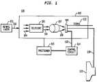
- the high-speed receiver cell 22comprises a fast photodetector and a high-speed amplifier (not shown in FIG. 2 ). When light falling on the receiver cell 22 is sufficiently strong, the cell 22 will be able to detect rapid fluctuations (modulations) in incident optical power.
- the amplifier in the receiver cellcontinuously monitors the output of the fast photodetector and turns the weak fluctuations into a signal sufficiently strong to drive the output line 25 . Further amplification and filtering can be carried out by the output buffer 26 before the signal leaves the chip to become the communication signal 27 .
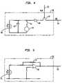
- FIG. 4shows an exemplary integrating circuit 40 which can be located in each imaging cell ( 21 of FIG. 2 ).
- a reset switch 41is first briefly connected, setting a reference voltage 42 across an integration capacitance 43 .
- Light falling on the photodiode 44generates a current which causes a floating node 45 to slowly discharge.
- the accumulated change in the voltage on the floating node 45is proportional to how much light has fallen since the cell was last reset and inversely proportional to the size of the capacitance 43 .
- the total capacitance 43comprises the capacitance of the photodiode 44 , the input capacitance of the amplifier 46 , and various stray capacitances.
- the floating node 45is connected to the input of the amplifier 46 .
- Another embodiment of the inventioncould use silicon photodetectors fabricated in the same substrate as the silicon circuits. Such an imaging array would be more sensitive to visible and near-infrared light than to currently standard communications wavelengths.
Landscapes
- Physics & Mathematics (AREA)
- Astronomy & Astrophysics (AREA)
- General Physics & Mathematics (AREA)
- Electromagnetism (AREA)
- Engineering & Computer Science (AREA)
- Computer Networks & Wireless Communication (AREA)
- Signal Processing (AREA)
- Optical Communication System (AREA)
- Transforming Light Signals Into Electric Signals (AREA)
Abstract
Description
- Each imaging cell integrates the electrical output of its photodetector over a relatively long time period.
- The receiver cell continuously monitors the output of its photodetector and continuously presents an amplified version to the output buffers.
- The imaging cells are sensitive to the distribution of light in space across their surfaces, but respond only to very slow variations with time
- The receiver cell is sensitive to a rapid time variation of the incoming light
- A high-speed data photodetector in the same plane as a tracking detector
- A high-speed data photodetector in the same plane as an acquisition imager
- A high-speed data photodetector fabricated at the center of a tracking detector and not needing to be aligned with a separate tracking detector
- No assembly of a data photodetector and tracking photodetector is necessary
- A separate means to track beam deviation is not necessary
- A separate means to acquire an image of the transmission source is not necessary
- Power-wasting and alignment-tricky beam-splitters are not necessary
- Only a single optical path is used by the receiver
- No precision alignment of multiple optical paths is necessary
- A much reduced component count leads to a simpler, lighter, more reliable and cheaper system
Claims (19)
Priority Applications (3)
| Application Number | Priority Date | Filing Date | Title |
|---|---|---|---|
| US10/964,266US7643755B2 (en) | 2003-10-13 | 2004-10-13 | Optical receiver comprising a receiver photodetector integrated with an imaging array |
| US11/206,555US20060055800A1 (en) | 2002-12-18 | 2005-08-18 | Adaptive solid state image sensor |
| US13/300,135US20120062774A1 (en) | 2003-10-13 | 2011-11-18 | Adaptive solid state image sensor |
Applications Claiming Priority (2)
| Application Number | Priority Date | Filing Date | Title |
|---|---|---|---|
| US51093303P | 2003-10-13 | 2003-10-13 | |
| US10/964,266US7643755B2 (en) | 2003-10-13 | 2004-10-13 | Optical receiver comprising a receiver photodetector integrated with an imaging array |
Related Child Applications (1)
| Application Number | Title | Priority Date | Filing Date |
|---|---|---|---|
| US11/206,555Continuation-In-PartUS20060055800A1 (en) | 2002-12-18 | 2005-08-18 | Adaptive solid state image sensor |
Publications (2)
| Publication Number | Publication Date |
|---|---|
| US20050191062A1 US20050191062A1 (en) | 2005-09-01 |
| US7643755B2true US7643755B2 (en) | 2010-01-05 |
Family
ID=34890381
Family Applications (1)
| Application Number | Title | Priority Date | Filing Date |
|---|---|---|---|
| US10/964,266Expired - Fee RelatedUS7643755B2 (en) | 2002-12-18 | 2004-10-13 | Optical receiver comprising a receiver photodetector integrated with an imaging array |
Country Status (1)
| Country | Link |
|---|---|
| US (1) | US7643755B2 (en) |
Cited By (11)
| Publication number | Priority date | Publication date | Assignee | Title |
|---|---|---|---|---|
| US20090110406A1 (en)* | 2007-10-24 | 2009-04-30 | Terrel Morris | Dynamic optical signal tracking on a detector array in a free space optical communication system |
| US20090202254A1 (en)* | 2008-02-12 | 2009-08-13 | Arun Kumar Majumdar | Wide field-of-view amplified fiber-retro for secure high data rate communications and remote data transfer |
| US20100019154A1 (en)* | 2008-07-28 | 2010-01-28 | Noble Peak Vision Corp. | Imaging apparatus and methods |
| US20100158536A1 (en)* | 2008-10-06 | 2010-06-24 | Astrium Sas | Optical Transceiver Assembly with Transmission-Direction Control |
| US8084739B2 (en) | 2008-07-16 | 2011-12-27 | Infrared Newco., Inc. | Imaging apparatus and methods |
| US8200094B1 (en)* | 2009-04-11 | 2012-06-12 | Applied Micro Circuits Corporation | System and method for free space optical connector alignment |
| US20130216241A1 (en)* | 2012-02-16 | 2013-08-22 | International Business Machines Corporation | Optical receiver using infinite impulse response decision feedback equalization |
| US20150188628A1 (en)* | 2013-12-27 | 2015-07-02 | Charles H. Chalfant, III | Acquisition, Tracking, and Pointing Apparatus for Free Space Optical Communications with Moving Focal Plane Array |
| US20160043801A1 (en)* | 2014-08-11 | 2016-02-11 | Leuze Electronic Gmbh + Co. Kg | Method for Aligning a Sensor Device |
| US20160134367A1 (en)* | 2013-07-01 | 2016-05-12 | Nokia Technologies Oy | Directional optical communications |
| US11196486B2 (en) | 2019-11-14 | 2021-12-07 | Analog Photonics LLC | Array-based free-space optical communication links |
Families Citing this family (11)
| Publication number | Priority date | Publication date | Assignee | Title |
|---|---|---|---|---|
| US20060055800A1 (en)* | 2002-12-18 | 2006-03-16 | Noble Device Technologies Corp. | Adaptive solid state image sensor |
| US7643755B2 (en) | 2003-10-13 | 2010-01-05 | Noble Peak Vision Corp. | Optical receiver comprising a receiver photodetector integrated with an imaging array |
| US7629661B2 (en)* | 2006-02-10 | 2009-12-08 | Noble Peak Vision Corp. | Semiconductor devices with photoresponsive components and metal silicide light blocking structures |
| US20100266290A1 (en)* | 2009-04-15 | 2010-10-21 | Honeywell International Inc. | Laser communication positioning system |
| US8436833B2 (en) | 2009-11-25 | 2013-05-07 | Corning Incorporated | Methods and apparatus for sensing touch events on a display |
| DE102010038479B4 (en)* | 2010-07-27 | 2018-01-04 | Universität Duisburg-Essen | Transmission device for free space transmission of optical signals and associated use |
| US8891977B2 (en)* | 2010-09-29 | 2014-11-18 | Supreme Architecture Ltd. | Receiver chip and method for on-chip multi-node visible light communication |
| CN104160366A (en) | 2011-11-28 | 2014-11-19 | 康宁股份有限公司 | Robust optical touch screen system and method using flat transparent sheet |
| WO2013081894A1 (en) | 2011-11-28 | 2013-06-06 | Corning Incorporated | Optical touch-screen systems and methods using a planar transparent sheet |
| US9880653B2 (en) | 2012-04-30 | 2018-01-30 | Corning Incorporated | Pressure-sensing touch system utilizing total-internal reflection |
| CN106464366A (en)* | 2014-01-10 | 2017-02-22 | 八河流资产有限责任公司 | Diverging Beam Communication System |
Citations (34)
| Publication number | Priority date | Publication date | Assignee | Title |
|---|---|---|---|---|
| US4823402A (en) | 1986-04-21 | 1989-04-18 | Trw Inc. | Agile optical beam steering system |
| US4939369A (en)* | 1988-10-04 | 1990-07-03 | Loral Fairchild Corporation | Imaging and tracking sensor designed with a sandwich structure |
| US5030004A (en)* | 1988-10-14 | 1991-07-09 | British Aerospace Public Limited Company | Process and apparatus for controlling the alignment of a transmit laser beam of a coherent detection optical communications transmitter/receiver terminal |
| JPH05183515A (en) | 1991-12-27 | 1993-07-23 | Mitsubishi Electric Corp | Optical space transmitter |
| US5401952A (en)* | 1991-10-25 | 1995-03-28 | Canon Kabushiki Kaisha | Signal processor having avalanche photodiodes |
| US5447117A (en) | 1987-08-08 | 1995-09-05 | Canon Kabushiki Kaisha | Crystal article, method for producing the same and semiconductor device utilizing the same |
| US5467204A (en) | 1991-12-09 | 1995-11-14 | Sharp Kabushiki Kaisha | Liquid crystal light valve with dual function as both optical-to-electrical and optical-to-optical transducer |
| US5770850A (en) | 1997-04-30 | 1998-06-23 | At&T Corp | Sensor array tracking and detection system having an alignment positioner |
| US5790291A (en) | 1995-12-07 | 1998-08-04 | Lucent Technologies Inc. | Beam steering and tracking of laser communication links by dual-quadrant tracker and photodiode assembly |
| US5953146A (en)* | 1997-01-30 | 1999-09-14 | At&T Corp. | Method and apparatus for tracking alignment in wireless optical communications |
| US6122084A (en)* | 1998-03-03 | 2000-09-19 | At&T Corp. | High dynamic range free-space optical communication receiver |
| US20020039833A1 (en) | 2000-08-04 | 2002-04-04 | Stmicroelectronics S.A. | Forming of quantum dots |
| US20020131121A1 (en)* | 2001-03-13 | 2002-09-19 | Muthu Jeganathan | Transceiver, system, and method for free-space optical communication and tracking |
| US6493490B1 (en) | 2000-12-18 | 2002-12-10 | Terabeam Corporation | Method and apparatus for receiving and aligning an optical communications beam with an integrated |
| US20020196506A1 (en)* | 2001-06-26 | 2002-12-26 | Zyoptics, Inc. | Atmospheric optical data transmission system |
| US20030013218A1 (en) | 2001-07-10 | 2003-01-16 | Motorola, Inc. | Structure and method for fabricating semiconductor structures and devices for detecting chemical reactant |
| US6509992B1 (en) | 1999-09-09 | 2003-01-21 | Nortel Networks Corporation | Free space optical interconnect system tolerant to misalignments and method of operation thereof |
| US6522440B1 (en) | 1999-04-28 | 2003-02-18 | Trw Inc. | Inter-satellite optical link track sensor |
| US20030034501A1 (en)* | 2001-08-16 | 2003-02-20 | Motorola, Inc. | Image sensor with high degree of functional integration |
| US20030067657A1 (en)* | 2001-09-07 | 2003-04-10 | Dimmler Wolfgang M. | Method and apparatus to compensate for atmospheric effects and target motion in laser communication system |
| US6577421B1 (en) | 1999-08-12 | 2003-06-10 | Hughes Electronics Corporation | Alignment system and method for optical satellite communication |
| US20030213915A1 (en)* | 2002-02-05 | 2003-11-20 | Calvin Chao | Photoconductor-on-active-pixel (POAP) sensor utilizing equal-potential pixel electrodes |
| WO2004008537A2 (en) | 2002-07-11 | 2004-01-22 | Qinetiq Limited | Photodetector circuits |
| US20040052465A1 (en)* | 2002-09-12 | 2004-03-18 | Alcatel | Receiver for a free space optics system which is able to evaluate the causes of a reduction of the received power |
| US6731415B1 (en) | 2002-03-28 | 2004-05-04 | Terabeam Corporation | Multi-aperture holographic optical element for use in a free space optical communication system |
| US20040121507A1 (en) | 2002-12-18 | 2004-06-24 | Bude Jeffrey Devin | Semiconductor devices with reduced active region deffects and unique contacting schemes |
| US6768876B1 (en) | 2000-07-28 | 2004-07-27 | Terabeam Corporation | Method and apparatus for tracking an optical communications system |
| US6775480B1 (en) | 1998-09-10 | 2004-08-10 | Nortel Networks Limited | Free space optical interconnect system |
| US20040156640A1 (en) | 2002-11-05 | 2004-08-12 | Dress William B. | Optical fan-out and broadcast interconnect |
| US20040258415A1 (en)* | 2003-06-18 | 2004-12-23 | Boone Bradley G. | Techniques for secure free space laser communications |
| US20050104089A1 (en) | 2002-02-05 | 2005-05-19 | Engelmann Michael G. | Visible/near infrared image sensor |
| US20050191062A1 (en) | 2003-10-13 | 2005-09-01 | Rafferty Conor S. | Optical receiver comprising a receiver photodetector integrated with an imaging array |
| US7292788B2 (en)* | 2003-01-31 | 2007-11-06 | Lockheed Martin Corporation | Multi-beam laser communications system and method |
| US7389052B2 (en)* | 2002-01-30 | 2008-06-17 | Texas Instruments Incorporated | Calibration method for station orientation |
- 2004
- 2004-10-13USUS10/964,266patent/US7643755B2/ennot_activeExpired - Fee Related
Patent Citations (34)
| Publication number | Priority date | Publication date | Assignee | Title |
|---|---|---|---|---|
| US4823402A (en) | 1986-04-21 | 1989-04-18 | Trw Inc. | Agile optical beam steering system |
| US5447117A (en) | 1987-08-08 | 1995-09-05 | Canon Kabushiki Kaisha | Crystal article, method for producing the same and semiconductor device utilizing the same |
| US4939369A (en)* | 1988-10-04 | 1990-07-03 | Loral Fairchild Corporation | Imaging and tracking sensor designed with a sandwich structure |
| US5030004A (en)* | 1988-10-14 | 1991-07-09 | British Aerospace Public Limited Company | Process and apparatus for controlling the alignment of a transmit laser beam of a coherent detection optical communications transmitter/receiver terminal |
| US5401952A (en)* | 1991-10-25 | 1995-03-28 | Canon Kabushiki Kaisha | Signal processor having avalanche photodiodes |
| US5467204A (en) | 1991-12-09 | 1995-11-14 | Sharp Kabushiki Kaisha | Liquid crystal light valve with dual function as both optical-to-electrical and optical-to-optical transducer |
| JPH05183515A (en) | 1991-12-27 | 1993-07-23 | Mitsubishi Electric Corp | Optical space transmitter |
| US5790291A (en) | 1995-12-07 | 1998-08-04 | Lucent Technologies Inc. | Beam steering and tracking of laser communication links by dual-quadrant tracker and photodiode assembly |
| US5953146A (en)* | 1997-01-30 | 1999-09-14 | At&T Corp. | Method and apparatus for tracking alignment in wireless optical communications |
| US5770850A (en) | 1997-04-30 | 1998-06-23 | At&T Corp | Sensor array tracking and detection system having an alignment positioner |
| US6122084A (en)* | 1998-03-03 | 2000-09-19 | At&T Corp. | High dynamic range free-space optical communication receiver |
| US6775480B1 (en) | 1998-09-10 | 2004-08-10 | Nortel Networks Limited | Free space optical interconnect system |
| US6522440B1 (en) | 1999-04-28 | 2003-02-18 | Trw Inc. | Inter-satellite optical link track sensor |
| US6577421B1 (en) | 1999-08-12 | 2003-06-10 | Hughes Electronics Corporation | Alignment system and method for optical satellite communication |
| US6509992B1 (en) | 1999-09-09 | 2003-01-21 | Nortel Networks Corporation | Free space optical interconnect system tolerant to misalignments and method of operation thereof |
| US6768876B1 (en) | 2000-07-28 | 2004-07-27 | Terabeam Corporation | Method and apparatus for tracking an optical communications system |
| US20020039833A1 (en) | 2000-08-04 | 2002-04-04 | Stmicroelectronics S.A. | Forming of quantum dots |
| US6493490B1 (en) | 2000-12-18 | 2002-12-10 | Terabeam Corporation | Method and apparatus for receiving and aligning an optical communications beam with an integrated |
| US20020131121A1 (en)* | 2001-03-13 | 2002-09-19 | Muthu Jeganathan | Transceiver, system, and method for free-space optical communication and tracking |
| US20020196506A1 (en)* | 2001-06-26 | 2002-12-26 | Zyoptics, Inc. | Atmospheric optical data transmission system |
| US20030013218A1 (en) | 2001-07-10 | 2003-01-16 | Motorola, Inc. | Structure and method for fabricating semiconductor structures and devices for detecting chemical reactant |
| US20030034501A1 (en)* | 2001-08-16 | 2003-02-20 | Motorola, Inc. | Image sensor with high degree of functional integration |
| US20030067657A1 (en)* | 2001-09-07 | 2003-04-10 | Dimmler Wolfgang M. | Method and apparatus to compensate for atmospheric effects and target motion in laser communication system |
| US7389052B2 (en)* | 2002-01-30 | 2008-06-17 | Texas Instruments Incorporated | Calibration method for station orientation |
| US20030213915A1 (en)* | 2002-02-05 | 2003-11-20 | Calvin Chao | Photoconductor-on-active-pixel (POAP) sensor utilizing equal-potential pixel electrodes |
| US20050104089A1 (en) | 2002-02-05 | 2005-05-19 | Engelmann Michael G. | Visible/near infrared image sensor |
| US6731415B1 (en) | 2002-03-28 | 2004-05-04 | Terabeam Corporation | Multi-aperture holographic optical element for use in a free space optical communication system |
| WO2004008537A2 (en) | 2002-07-11 | 2004-01-22 | Qinetiq Limited | Photodetector circuits |
| US20040052465A1 (en)* | 2002-09-12 | 2004-03-18 | Alcatel | Receiver for a free space optics system which is able to evaluate the causes of a reduction of the received power |
| US20040156640A1 (en) | 2002-11-05 | 2004-08-12 | Dress William B. | Optical fan-out and broadcast interconnect |
| US20040121507A1 (en) | 2002-12-18 | 2004-06-24 | Bude Jeffrey Devin | Semiconductor devices with reduced active region deffects and unique contacting schemes |
| US7292788B2 (en)* | 2003-01-31 | 2007-11-06 | Lockheed Martin Corporation | Multi-beam laser communications system and method |
| US20040258415A1 (en)* | 2003-06-18 | 2004-12-23 | Boone Bradley G. | Techniques for secure free space laser communications |
| US20050191062A1 (en) | 2003-10-13 | 2005-09-01 | Rafferty Conor S. | Optical receiver comprising a receiver photodetector integrated with an imaging array |
Non-Patent Citations (2)
| Title |
|---|
| Colace et al: "Efficient high-speed near-infrared Ge photodetectors integrated on Si Substrates", Applied Physics Letter, vol. 76, No. 10, Mar. 6, 2000, pp. 1231-1233.* |
| Search Report and Written Opinion from PCT International Application No. PCT/US06/31591 mailed Nov. 2, 2007. |
Cited By (22)
| Publication number | Priority date | Publication date | Assignee | Title |
|---|---|---|---|---|
| US8009991B2 (en)* | 2007-10-24 | 2011-08-30 | Hewlett-Packard Development Company, L.P. | Dynamic optical signal tracking on a detector array in a free space optical communication system |
| US20090110406A1 (en)* | 2007-10-24 | 2009-04-30 | Terrel Morris | Dynamic optical signal tracking on a detector array in a free space optical communication system |
| US20090202254A1 (en)* | 2008-02-12 | 2009-08-13 | Arun Kumar Majumdar | Wide field-of-view amplified fiber-retro for secure high data rate communications and remote data transfer |
| US8301032B2 (en)* | 2008-02-12 | 2012-10-30 | Arun Kumar Majumdar | Wide field-of-view amplified fiber-retro for secure high data rate communications and remote data transfer |
| US8084739B2 (en) | 2008-07-16 | 2011-12-27 | Infrared Newco., Inc. | Imaging apparatus and methods |
| US8294100B2 (en) | 2008-07-16 | 2012-10-23 | Infrared Newco, Inc. | Imaging apparatus and methods |
| US20100019154A1 (en)* | 2008-07-28 | 2010-01-28 | Noble Peak Vision Corp. | Imaging apparatus and methods |
| US8686365B2 (en) | 2008-07-28 | 2014-04-01 | Infrared Newco, Inc. | Imaging apparatus and methods |
| US8588617B2 (en)* | 2008-10-06 | 2013-11-19 | Astrium Sas | Optical transceiver assembly with transmission-direction control |
| US20100158536A1 (en)* | 2008-10-06 | 2010-06-24 | Astrium Sas | Optical Transceiver Assembly with Transmission-Direction Control |
| US8200094B1 (en)* | 2009-04-11 | 2012-06-12 | Applied Micro Circuits Corporation | System and method for free space optical connector alignment |
| US20130214135A1 (en)* | 2012-02-16 | 2013-08-22 | International Business Machines Corporation | Optical receiver using infinite impulse response decision feedback equalization |
| US20130216241A1 (en)* | 2012-02-16 | 2013-08-22 | International Business Machines Corporation | Optical receiver using infinite impulse response decision feedback equalization |
| US8798484B2 (en)* | 2012-02-16 | 2014-08-05 | International Business Machines Corporation | Optical receiver using infinite impulse response decision feedback equalization |
| US8977138B2 (en)* | 2012-02-16 | 2015-03-10 | International Business Machines Corporation | Optical receiver using infinite impulse response decision feedback equalization |
| US20160134367A1 (en)* | 2013-07-01 | 2016-05-12 | Nokia Technologies Oy | Directional optical communications |
| US9692508B2 (en)* | 2013-07-01 | 2017-06-27 | Nokia Technologies Oy | Directional optical communications |
| US20150188628A1 (en)* | 2013-12-27 | 2015-07-02 | Charles H. Chalfant, III | Acquisition, Tracking, and Pointing Apparatus for Free Space Optical Communications with Moving Focal Plane Array |
| US9800332B2 (en)* | 2013-12-27 | 2017-10-24 | Space Photonics, Inc. | Acquisition, tracking, and pointing apparatus for free space optical communications with moving focal plane array |
| US20160043801A1 (en)* | 2014-08-11 | 2016-02-11 | Leuze Electronic Gmbh + Co. Kg | Method for Aligning a Sensor Device |
| US9503184B2 (en)* | 2014-08-11 | 2016-11-22 | Leuze Electronic Gmbh + Co. Kg | Method for aligning a sensor device |
| US11196486B2 (en) | 2019-11-14 | 2021-12-07 | Analog Photonics LLC | Array-based free-space optical communication links |
Also Published As
| Publication number | Publication date |
|---|---|
| US20050191062A1 (en) | 2005-09-01 |
Similar Documents
| Publication | Publication Date | Title |
|---|---|---|
| US7643755B2 (en) | Optical receiver comprising a receiver photodetector integrated with an imaging array | |
| US7230227B2 (en) | Lenslet/detector array assembly for high data rate optical communications | |
| US6414746B1 (en) | 3-D imaging multiple target laser radar | |
| US10931372B2 (en) | Dual-mode imaging receiver | |
| US7397019B1 (en) | Light sensor module, focused light sensor array, and an air vehicle so equipped | |
| US9215386B2 (en) | Detector pixel signal readout circuit using an AC signal component in implementing an event detection mode per pixel | |
| US20020131121A1 (en) | Transceiver, system, and method for free-space optical communication and tracking | |
| US20070076481A1 (en) | Multimode focal plane array with electrically isolated commons for independent sub-array biasing | |
| US20140293263A1 (en) | LIDAR Comprising Polyhedron Transmission and Receiving Scanning Element | |
| CN112491470B (en) | Alignment tracking wireless optical communication device and method using communication optical peripheral part | |
| US11280885B2 (en) | LADAR receiver | |
| JPH10336112A (en) | System and method for optical communication beam tracking and for data receiving from the beam | |
| US5925883A (en) | Staring IR-FPA with CCD-based image motion compensation | |
| CN114859288A (en) | Single photon detection array laser tracking angle measurement and communication distance measurement device and method | |
| US6522440B1 (en) | Inter-satellite optical link track sensor | |
| CN114442109A (en) | Large dynamic range hybrid solid-state lidar system based on transceiver array module | |
| DK2143264T3 (en) | LASER IMPULSE MATRIX DETECTOR WITH QUICK SUMMARY | |
| JP2829898B2 (en) | Optical communication device | |
| US8587776B2 (en) | Miniature laser seeker electro-optics | |
| US20050169646A1 (en) | Lincoln distributed optical receiver array | |
| JP3052906B2 (en) | Spatial optical transmission equipment | |
| Joyner et al. | A CMOS imaging diversity receiver chip with a flip-chip integrated detector array for optical wireless links | |
| US4904086A (en) | Light alignment detection device | |
| Browder et al. | Three-dimensional imaging sensors program | |
| CN114142943B (en) | Single photon ranging tracking and few photon communication integrated receiving device and method |
Legal Events
| Date | Code | Title | Description |
|---|---|---|---|
| AS | Assignment | Owner name:NOBLE DEVICE TECHNOLOGIES CORPORATION, MASSACHUSET Free format text:ASSIGNMENT OF ASSIGNORS INTEREST;ASSIGNORS:RAFFERTY, CONOR S.;KING, CLIFFORD;REEL/FRAME:018791/0888 Effective date:20070111 | |
| AS | Assignment | Owner name:NOBLE PEAK VISION CORP., MASSACHUSETTS Free format text:CHANGE OF NAME;ASSIGNOR:NOBLE DEVICE TECHNOLOGIES CORPORATION;REEL/FRAME:019874/0166 Effective date:20070309 | |
| STCF | Information on status: patent grant | Free format text:PATENTED CASE | |
| CC | Certificate of correction | ||
| AS | Assignment | Owner name:INFRARED NEWCO INC., ARIZONA Free format text:ASSIGNMENT OF ASSIGNORS INTEREST;ASSIGNOR:NOBLEPEAK VISION CORP.;REEL/FRAME:026955/0795 Effective date:20110720 | |
| REMI | Maintenance fee reminder mailed | ||
| FPAY | Fee payment | Year of fee payment:4 | |
| SULP | Surcharge for late payment | ||
| FPAY | Fee payment | Year of fee payment:8 | |
| AS | Assignment | Owner name:SEMIKING LLC, MASSACHUSETTS Free format text:NOTICE OF EXCLUSIVE LICENSE AND PURCHASE OPTION;ASSIGNOR:INFRARED LABORATORIES, INC.;REEL/FRAME:049149/0252 Effective date:20190509 | |
| FEPP | Fee payment procedure | Free format text:MAINTENANCE FEE REMINDER MAILED (ORIGINAL EVENT CODE: REM.); ENTITY STATUS OF PATENT OWNER: SMALL ENTITY | |
| LAPS | Lapse for failure to pay maintenance fees | Free format text:PATENT EXPIRED FOR FAILURE TO PAY MAINTENANCE FEES (ORIGINAL EVENT CODE: EXP.); ENTITY STATUS OF PATENT OWNER: SMALL ENTITY | |
| STCH | Information on status: patent discontinuation | Free format text:PATENT EXPIRED DUE TO NONPAYMENT OF MAINTENANCE FEES UNDER 37 CFR 1.362 | |
| FP | Lapsed due to failure to pay maintenance fee | Effective date:20220105 |