US7643357B2 - System and method for integrating dynamic leakage reduction with write-assisted SRAM architecture - Google Patents
System and method for integrating dynamic leakage reduction with write-assisted SRAM architectureDownload PDFInfo
- Publication number
- US7643357B2 US7643357B2US12/032,798US3279808AUS7643357B2US 7643357 B2US7643357 B2US 7643357B2US 3279808 AUS3279808 AUS 3279808AUS 7643357 B2US7643357 B2US 7643357B2
- Authority
- US
- United States
- Prior art keywords
- voltage
- power line
- write
- pfet
- sub arrays
- Prior art date
- Legal status (The legal status is an assumption and is not a legal conclusion. Google has not performed a legal analysis and makes no representation as to the accuracy of the status listed.)
- Active, expires
Links
- 230000009467reductionEffects0.000titleclaimsabstractdescription25
- 238000000034methodMethods0.000titleclaimsdescription16
- 238000003491arrayMethods0.000claimsabstractdescription41
- 230000000295complement effectEffects0.000claimsdescription6
- 230000003278mimic effectEffects0.000claimsdescription5
- 230000007704transitionEffects0.000claimsdescription3
- 238000010586diagramMethods0.000description12
- 230000008859changeEffects0.000description4
- 238000013459approachMethods0.000description3
- 230000006870functionEffects0.000description3
- 230000004913activationEffects0.000description2
- 230000007423decreaseEffects0.000description2
- 238000005516engineering processMethods0.000description2
- 230000014759maintenance of locationEffects0.000description2
- 238000005457optimizationMethods0.000description2
- 230000001052transient effectEffects0.000description2
- 230000009849deactivationEffects0.000description1
- 230000003247decreasing effectEffects0.000description1
- 230000007812deficiencyEffects0.000description1
- 230000009977dual effectEffects0.000description1
- 230000006872improvementEffects0.000description1
- 239000000463materialSubstances0.000description1
- 229910044991metal oxideInorganic materials0.000description1
- 150000004706metal oxidesChemical class0.000description1
- 230000004048modificationEffects0.000description1
- 238000012986modificationMethods0.000description1
- 239000004065semiconductorSubstances0.000description1
- 238000004513sizingMethods0.000description1
- 230000003068static effectEffects0.000description1
Images


Classifications
- G—PHYSICS
- G11—INFORMATION STORAGE
- G11C—STATIC STORES
- G11C11/00—Digital stores characterised by the use of particular electric or magnetic storage elements; Storage elements therefor
- G11C11/21—Digital stores characterised by the use of particular electric or magnetic storage elements; Storage elements therefor using electric elements
- G11C11/34—Digital stores characterised by the use of particular electric or magnetic storage elements; Storage elements therefor using electric elements using semiconductor devices
- G11C11/40—Digital stores characterised by the use of particular electric or magnetic storage elements; Storage elements therefor using electric elements using semiconductor devices using transistors
- G11C11/41—Digital stores characterised by the use of particular electric or magnetic storage elements; Storage elements therefor using electric elements using semiconductor devices using transistors forming static cells with positive feedback, i.e. cells not needing refreshing or charge regeneration, e.g. bistable multivibrator or Schmitt trigger
- G11C11/413—Auxiliary circuits, e.g. for addressing, decoding, driving, writing, sensing, timing or power reduction
- G11C11/417—Auxiliary circuits, e.g. for addressing, decoding, driving, writing, sensing, timing or power reduction for memory cells of the field-effect type
Definitions
- the present inventionrelates generally to integrated circuit memory devices and, more particularly, to a system and method for integrating dynamic leakage reduction with a write-assisted SRAM architecture.
- RAMrandom access memory
- SRAMstatic RAM
- DRAMdynamic RAM
- RAMis typically used as main memory in a computer environment. RAM is generally volatile, in that once power is turned off, all data stored in the RAM is lost.
- a typical SRAM deviceincludes an array of individual SRAM cells. Each SRAM cell is capable of storing a binary voltage value therein, which voltage value represents a logical data bit (e.g., “0” or “1”).
- One existing configuration for an SRAM cellincludes a pair of cross-coupled devices such as inverters. With CMOS (complementary metal oxide semiconductor) technology, the inverters further include a pull-up PFET (p-channel) transistor connected to a complementary pull-down NFET (n-channel) transistor. The inverters, connected in a cross-coupled configuration, act as a latch that stores the data bit therein so long as power is supplied to the memory array.
- a pair of access transistors or pass gateswhen activated by a word line selectively couples the inverters to a pair of complementary bit lines.
- Other SRAM cell designsmay include a different number of transistors, e.g., 4T, 8T, etc.
- SRAM cellsThe design of SRAM cells has traditionally involved a compromise between the read and write functions of the memory cell to maintain cell stability, read performance and write performance.
- the transistors which make up the cross-coupled latchmust be weak enough to be overdriven during a write operation, while also strong enough to maintain their data value when driving a bit line during a read operation.
- the access transistors that connect the cross-coupled cell nodes to the true and complement bit linesaffect both the stability and performance of the cell.
- a single pair of access transistorsis conventionally used for both read and write access to the cell.
- the gatesare driven to a digital value in order to switch the transistors between an on and off state.
- the optimization of an access for a write operationwould drive the reduction of the on-resistance (R on ) for the device.
- the optimization of an access transistor for a read operationdrives an increase in R on in order to isolate the cell from the bit line capacitance and prevent a cell disturb.
- the systemincludes a plurality of SRAM cells arranged into rows and columns within one or more sub arrays; power line selection circuitry associated with each column of the one or more sub arrays, the power line selection circuitry controlled by a selection signal that selects the associated sub array for a read or write operation, and by a column write signal that selects one of the columns of each of the one or more sub arrays; wherein the power line selection circuitry is configured to locally convert a first voltage, corresponding to a cell supply voltage for a read operation of the SRAM cells, to a second voltage to be supplied to each SRAM cell selected for a write operation thereto, the second voltage being lower than the first voltage so as to facilitate a write function; and wherein the power line selection circuitry is further configured to locally convert the first voltage to a third voltage to be supplied to power lines in unselected sub array
- a method for integrating dynamic leakage reduction with a write-assisted SRAM architectureincludes configuring a plurality of SRAM cells into rows and columns within one or more sub arrays; configuring power line selection circuitry associated with each column of the one or more sub arrays, the power line selection circuitry controlled by a selection signal that selects the associated sub array for a read or write operation, and by a column write signal that selects one of the columns of each of the one or more sub arrays; wherein the power line selection circuitry is configured to locally convert a first voltage, corresponding to a cell supply voltage for a read operation of the SRAM cells, to a second voltage to be supplied to each SRAM cell selected for a write operation thereto, the second voltage being lower than the first voltage so as to facilitate a write function; and wherein the power line selection circuitry is further configured to locally convert the first voltage to a third voltage to be supplied to power lines in unselected sub arrays, the third voltage also being lower than the first voltage so as to facilitate dynamic leakage reduction.
- FIG. 1( a )is a schematic diagram of an existing SRAM system in which the transistor devices are sized so as to optimize the read operation;
- FIG. 1( b )is a schematic diagram of an existing SRAM system in which the transistor devices are sized so as to optimize the write operation;
- FIG. 2is a schematic diagram of an existing SRAM system having separately configured write-assist and leakage savings features
- FIG. 3is a schematic diagram of an SRAM cell, in accordance with an embodiment of the invention.
- FIG. 4is a schematic diagram of a system for integrating dynamic leakage reduction with a write-assisted SRAM architecture, in accordance with an embodiment of the invention
- FIG. 5is a schematic diagram of a system for integrating dynamic leakage reduction with a write-assisted SRAM architecture, in accordance with an alternative embodiment of the invention.
- FIG. 6is a schematic diagram of a system for integrating dynamic leakage reduction with a write-assisted SRAM architecture, in accordance with still an alternative embodiment of the invention.
- the present architectureimproves both a reduced write voltage level and a leakage savings through a common circuit that integrates a write-assist capability (i.e., operation of an SRAM array at selected first and second cell voltage levels, depending on a read or write) with dynamic leakage control.
- a write-assist capabilityi.e., operation of an SRAM array at selected first and second cell voltage levels, depending on a read or write
- dynamic leakage controli.e., operation of an SRAM array at selected first and second cell voltage levels, depending on a read or write
- FIGS. 1( a ) and 1 ( b )there is shown a pair of schematic diagrams illustrating an existing SRAM system in which the transistor devices are sized so as to optimize the read operation, in the case of FIG. 1( a ), and the write operation, in the case of FIG. 1( b ).
- both the pull up transistors (T pu ) and the pull down transistors (T pd ) of the 6T SRAM cellhave a relatively large conductive strength with respect to the access or “pass gate” transistors (T pg ) of the SRAM cell.
- the pull down transistors 104 of the sense amplifier latchhave a relatively large conductive strength
- the write driver switches 106 that couple the write driver data lines (DLTW, DLCW) to the cell bit lines (BLT, BLC)have a relatively small conductive strength.
- FIG. 2is a schematic diagram illustrating one existing approach for implementing a sub array 200 in an SRAM system (e.g., having 64 word lines) including both write-assist circuitry 202 and leakage savings circuitry 204 .
- Each SRAM columnhas its own individual power line with the upper portion 206 thereof coupled to a pair of PFET select transistors, generally depicted at 208 .
- a first of the PFET select transistor pairconnects the power line to the nominal supply or rail voltage (V DD ) for normal read or unselected (and half-selected) operations.
- V DDnominal supply or rail voltage
- the selected SRAM column for writingis connected to an external write power supply (V WR ) through the second of the PFET select transistor pair, wherein the external power supply voltage V WR is lower than the nominal rail voltage V DD .
- V WRmay be a voltage threshold value (V t ) of a PFET/NFET lower than V DD .
- the lower write voltage V WRcould be generated on-chip, but at a cost of increased device area.
- each columnhas unique decode logic 210 for the PFET select transistors pair 208 so that the lower voltage (V WR ) is supplied only to those columns that are actually writing.
- FIG. 2further illustrates the separate leakage savings circuitry 204 coupled between a common terminal 212 of a virtual ground node and ground. More specifically, the circuitry 204 includes a plurality of binary weighted “sleep” NFETs controlled by signals F 1 , F 2 , F 3 , etc., to provide optimum leakage savings without compromising data retention.
- the circuitry 204includes a plurality of binary weighted “sleep” NFETs controlled by signals F 1 , F 2 , F 3 , etc., to provide optimum leakage savings without compromising data retention.
- a “soft” ground nodei.e., terminal 212
- the degree to which the voltage across the SRAM cells is reducedbecomes adjustable in accordance with the control signals applied to the gates of the sleep NFETs.
- each sub array 200 of the systemincludes individual logic devices 208 , 210 for each column.
- FIG. 3An exemplary SRAM cell 300 suitable for use in the architecture is illustrated in FIG. 3 .
- the cell 300is optimized for a read operation, wherein the beta ratio is made larger with respect to conventional designs, and the PFET pull-up devices are also made stronger.
- the threshold voltage V t of the pull up transistors of the cell 300is decreased by about 150 mV with respect to a balanced device while the threshold voltage of the access transistor is increased by about 50 mV with respect to a balanced device.
- the cell 300is configured to provide excellent read stability margins.
- the power line voltage V PL applied to the cell 300will vary, depending upon whether the cell is being read, written to, or the sub array of the cell is not activated.
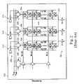
- FIG. 4there is shown a schematic diagram of a system 400 for integrating dynamic leakage reduction with a write-assisted SRAM architecture, in accordance with an embodiment of the invention.
- the SRAM arrayis divided into sub arrays which are independently activated by selection signals “SUBSEL_n”.
- selection signals “SUBSEL_n”For ease of illustration, two such sub arrays are depicted in FIG. 4 (sub array 0 , sub array 1 , selected by sub array decode signals, SUBSEL_ 0 and SUBSEL_ 1 , respectively).
- the number of actual sub arrays in an ASIC compilable SRAMmay vary from 1 to as many as 16, for example.
- the sub arrays 402are further divided into columns that receive power from an individual power line (PL 0 -PL 3 ) coupled to a cell voltage supply (V DD ) through a header PFET Tp.
- the voltage level supplied to the SRAM cells (labeled “MC” in FIG. 4 ) coupled to a given power lineis controlled by both the SUBSEL_n sub array decode signal and by the write lines (WRL 0 -WRL 3 ) decoded from column select addresses. It will be noted that the write lines are common across all sub arrays 402 in order to save area.
- each sub array columnhas a power line selection circuit 404 (transistors Ta, Tr, Tp) responsive to the associated “SUBSEL_n” decode signal and the associated “WRLn” column write line.
- An inverter device 406 associated with each SUBSEL_n inputgenerates a “Pseln” signal on a control line common to each transistor Ta of the power line selection circuits 404 .
- the selection circuit 404passes V DD to the local power line for a read operation, or generates V DD -V t locally and passes it to the power line for a write operation as described more fully below.
- the “WRLn” column write linesare high (which represents a deactivated state) and a given sub array decode signal (e.g., SUBSEL_ 0 ) is enabled so as to discharge the associated “Pseln” (e.g., Psel 0 ) node. This will also discharge the gates of each Tp device in the selected sub array (through conductive NFET Ta) so as to couple the power line to a full V DD voltage.
- a given sub array decode signale.g., SUBSEL_ 0
- any one columnmay be written to without affecting the voltage level of the half-selected columns.
- write decode address circuitry 408is used to select one of the WRLn column write lines to discharge. This isolates the gate of Tp from the grounded Pseln line (through deactivation of NFET Ta) and enables PFET Tr to shunt the gate and drain of Tp. As a result, PFET Tp acts as a diode, thereby enabling the partial discharge of the selected power line and lowering the voltage applied to the cell from V DD in an amount by the threshold voltage of Tp (V DD -V T Tp). Stated another way, the lower write-assist voltage is locally generated from the supply rail voltage V DD , as opposed to providing a separate and possibly off-chip voltage.
- the write decode address circuitry 408 for the write select lines WRLnis shared with all sub arrays to minimize area overhead (as opposed to the system of FIG. 2 where each column of each sub array has decode circuitry 210 ).
- unselected sub arraysare placed in a leakage-savings mode without compromising data retention.
- the Psel lines for unselected sub arraysare driven to V DD , since those SUBSEL signals are low and thus the corresponding inverters 406 drive the Psel lines to V DD .
- the gate of NFET device Ta in unselected write columnsis active to weakly pass V DD , less the threshold voltage of NFET Ta (i.e., V DD -V T Ta) to the gate of header device Tp and decrease its drive. As a result, the voltage on the unselected power lines of unselected sub arrays drops by an amount corresponding to the threshold voltage of NFET Ta.
- Power lines in unselected sub arraysmay see a small change in voltage as common write lines may be activated during write cycles to selected sub arrays.
- the gate voltage of PFET header device Tpmay switch from V DD -V T Ta to V DD -V T Tp. That is, the voltage on the gate of Tp temporarily transitions from the voltage on the Psel line to the cell power line.
- this small transient changeonly lasts during the short WL activation duration.
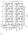
- FIG. 5is a schematic diagram of a system 500 for integrating dynamic leakage reduction with a write-assisted SRAM architecture, in accordance with an alternative embodiment of the invention.
- the embodiment of FIG. 5addresses the change of gate voltage of device Tp for unselected sub arrays while selected sub arrays are writing.
- a diode configured PFET Tp 1is coupled between the inverter 406 and the supply rail V DD .
- the corresponding Pseln linesare driven to V DD -V T Tp 1 for unselected sub arrays, instead of to V DD .
- low V T devicesare used for NFET Ta so that a full V DD -V T Tp 1 voltage is established at the gate of PFET Tp.
- a mimic power lineis associated with dummy cells in order to preserve the ratio between PFET Tp and the leakage for each column.
- PLMmimic power line
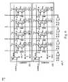
- FIG. 6is a schematic diagram of a system 600 for integrating dynamic leakage reduction with a write-assisted SRAM architecture, in accordance with still an alternative embodiment of the invention.
- the system 600is configured to further assist with the discharge of the cell power lines during write operations.
- the power line selection circuits 604include an additional PFET device Td added between the cell power line and ground, with the gate of Td also coupled to the associated column write line. Upon activation of Td during a write operation, the associated power lines quickly drop to V DD -V T Tp during write operations.
- This additional PFET devicemay be desirable for technologies where cell leakage currents or cell transient write-currents may be too small to discharge the PL node quickly enough to assist the write operation.
- the disclosed SRAM architecture embodimentsachieve about 80% of the leakage reduction benefits of the separately configured sleep footer NFETs in the architecture of FIG. 2 without the area penalty associated therewith.
- write-assist circuits and the sleep-NFETs of the prior artadd about 8% to SRAM area
- the present embodimentsadd only about 2-3% to SRAM area and therefore offer a denser solution with about 80% of the leakage reduction benefits.
- the SRAM architecture embodimentsprovide both improved voltage range and improved reduction in leakage current using a single integrated circuit scheme for write-assist and leakage control, which decreases device complexity and without the use of additional/external voltage supplies.
Landscapes
- Engineering & Computer Science (AREA)
- Microelectronics & Electronic Packaging (AREA)
- Computer Hardware Design (AREA)
- Static Random-Access Memory (AREA)
Abstract
Description
Claims (20)
Priority Applications (1)
| Application Number | Priority Date | Filing Date | Title |
|---|---|---|---|
| US12/032,798US7643357B2 (en) | 2008-02-18 | 2008-02-18 | System and method for integrating dynamic leakage reduction with write-assisted SRAM architecture |
Applications Claiming Priority (1)
| Application Number | Priority Date | Filing Date | Title |
|---|---|---|---|
| US12/032,798US7643357B2 (en) | 2008-02-18 | 2008-02-18 | System and method for integrating dynamic leakage reduction with write-assisted SRAM architecture |
Publications (2)
| Publication Number | Publication Date |
|---|---|
| US20090207650A1 US20090207650A1 (en) | 2009-08-20 |
| US7643357B2true US7643357B2 (en) | 2010-01-05 |
Family
ID=40954963
Family Applications (1)
| Application Number | Title | Priority Date | Filing Date |
|---|---|---|---|
| US12/032,798Active2028-04-30US7643357B2 (en) | 2008-02-18 | 2008-02-18 | System and method for integrating dynamic leakage reduction with write-assisted SRAM architecture |
Country Status (1)
| Country | Link |
|---|---|
| US (1) | US7643357B2 (en) |
Cited By (21)
| Publication number | Priority date | Publication date | Assignee | Title |
|---|---|---|---|---|
| US20090285039A1 (en)* | 2008-05-15 | 2009-11-19 | International Business Machines Corporation | Method and apparatus for locally generating a virtual ground for write assist on column selected sram cells |
| US20100002495A1 (en)* | 2008-07-03 | 2010-01-07 | International Business Machines Corporation | Column Selectable Self-Biasing Virtual Voltages for SRAM Write Assist |
| US20100097844A1 (en)* | 2008-10-22 | 2010-04-22 | Jack Liu | Write-Assist SRAM Cell |
| US20120013319A1 (en)* | 2010-07-14 | 2012-01-19 | Arm Limited | Power control apparatus and method |
| US20120163103A1 (en)* | 2010-12-22 | 2012-06-28 | Hafez Walid M | Memory cell using bti effects in high-k metal gate mos |
| US8363453B2 (en) | 2010-12-03 | 2013-01-29 | International Business Machines Corporation | Static random access memory (SRAM) write assist circuit with leakage suppression and level control |
| US20130194859A1 (en)* | 2012-01-27 | 2013-08-01 | Taiwan Semiconductor Manufacturing Co., Ltd. | Method and apparatus for switching power in a dual rail memory |
| US8520429B2 (en) | 2011-05-05 | 2013-08-27 | International Business Machines Corporation | Data dependent SRAM write assist |
| US8526228B2 (en) | 2012-01-06 | 2013-09-03 | International Business Machines Corporation | 8-transistor SRAM cell design with outer pass-gate diodes |
| US8531871B2 (en) | 2012-01-06 | 2013-09-10 | International Business Machines Corporation | 8-transistor SRAM cell design with Schottky diodes |
| US8619465B2 (en) | 2012-01-06 | 2013-12-31 | International Business Machines Corporation | 8-transistor SRAM cell design with inner pass-gate junction diodes |
| US20140092695A1 (en)* | 2012-10-02 | 2014-04-03 | Taiwan Semiconductor Manufacturing Company Limited | Header circuit for controlling supply voltage of a cell |
| US20140293680A1 (en)* | 2005-08-02 | 2014-10-02 | Renesas Electronics Corporation | Semiconductor memory device for stably reading and writing data |
| DE102012217578B4 (en)* | 2011-12-09 | 2016-07-28 | Globalfoundries Inc. | Fine granular power gating |
| US9548104B1 (en) | 2015-06-30 | 2017-01-17 | International Business Machines Corporation | Boost control to improve SRAM write operation |
| US9570155B2 (en)* | 2015-06-09 | 2017-02-14 | Globalfoundries Inc. | Circuit to improve SRAM stability |
| US9940999B2 (en) | 2016-06-22 | 2018-04-10 | Darryl G. Walker | Semiconductor devices, circuits and methods for read and/or write assist of an SRAM circuit portion based on voltage detection and/or temperature detection circuits |
| US10163524B2 (en) | 2016-06-22 | 2018-12-25 | Darryl G. Walker | Testing a semiconductor device including a voltage detection circuit and temperature detection circuit that can be used to generate read assist and/or write assist in an SRAM circuit portion and method therefor |
| US10446223B1 (en) | 2018-08-29 | 2019-10-15 | Bitfury Group Limited | Data storage apparatus, and related systems and methods |
| US20230080591A1 (en)* | 2021-09-15 | 2023-03-16 | DXCorr Design Inc. | Low standby leakage implementation for static random access memory |
| US11955171B2 (en) | 2021-09-15 | 2024-04-09 | Mavagail Technology, LLC | Integrated circuit device including an SRAM portion having end power select circuits |
Families Citing this family (14)
| Publication number | Priority date | Publication date | Assignee | Title |
|---|---|---|---|---|
| US8395923B2 (en)* | 2008-12-30 | 2013-03-12 | Intel Corporation | Antifuse programmable memory array |
| US8101471B2 (en)* | 2008-12-30 | 2012-01-24 | Intel Corporation | Method of forming programmable anti-fuse element |
| TWI425509B (en)* | 2009-11-17 | 2014-02-01 | Univ Hsiuping Sci & Tech | Dual port sram having a discharging path |
| US20110149667A1 (en)* | 2009-12-23 | 2011-06-23 | Fatih Hamzaoglu | Reduced area memory array by using sense amplifier as write driver |
| US8982659B2 (en)* | 2009-12-23 | 2015-03-17 | Intel Corporation | Bitline floating during non-access mode for memory arrays |
| US9218881B2 (en)* | 2012-10-23 | 2015-12-22 | Sandisk Technologies Inc. | Flash memory blocks with extended data retention |
| US9299396B1 (en) | 2014-07-15 | 2016-03-29 | Altera Corporation | Programmable integrated circuits with in-operation reconfiguration capability |
| US9916874B2 (en) | 2014-08-15 | 2018-03-13 | Taiwan Semiconductor Manufacturing Company, Ltd. | Memory architecture having first and second voltages |
| US11211116B2 (en)* | 2019-09-27 | 2021-12-28 | Taiwan Semiconductor Manufacturing Co., Ltd. | Embedded SRAM write assist circuit |
| KR102742853B1 (en)* | 2020-02-26 | 2024-12-13 | 삼성전자주식회사 | Memory device for reliable write operation and operating method thereof |
| WO2021231384A1 (en)* | 2020-05-14 | 2021-11-18 | Qualcomm Incorporated | Low leakage core power lowering (cpe) write assist scheme |
| US12165700B2 (en)* | 2021-09-29 | 2024-12-10 | Advanced Micro Devices, Inc. | SRAM power savings and write assist |
| WO2025029551A1 (en)* | 2023-08-01 | 2025-02-06 | Google Llc | Driver for a memory-in-pixel display |
| US20250046367A1 (en)* | 2023-08-02 | 2025-02-06 | Taiwan Semiconductor Manufacturing Company, Ltd. | Semiconductor devices and methods of manufacturing thereof |
Citations (11)
| Publication number | Priority date | Publication date | Assignee | Title |
|---|---|---|---|---|
| US4926383A (en) | 1988-02-02 | 1990-05-15 | National Semiconductor Corporation | BiCMOS write-recovery circuit |
| US5058067A (en) | 1990-06-06 | 1991-10-15 | National Semiconductor Corporation | Individual bit line recovery circuits |
| US5715191A (en)* | 1995-10-25 | 1998-02-03 | Matsushita Electric Industrial Co., Ltd. | Static random access memory having variable supply voltages to the memory cells and method of operating thereof |
| US5910922A (en) | 1997-08-05 | 1999-06-08 | Integrated Device Technology, Inc. | Method for testing data retention in a static random access memory using isolated Vcc supply |
| US20030189849A1 (en)* | 2002-04-05 | 2003-10-09 | Muhammad Khellah | Sram array with dynamic voltage for reducing active leakage power |
| US6738305B1 (en) | 2002-07-25 | 2004-05-18 | Taiwan Semiconductor Manufacturing Company | Standby mode circuit design for SRAM standby power reduction |
| US6798688B2 (en)* | 2002-11-29 | 2004-09-28 | International Business Machines Corp. | Storage array such as a SRAM with reduced power requirements |
| US6804143B1 (en) | 2003-04-02 | 2004-10-12 | Cogent Chipware Inc. | Write-assisted SRAM bit cell |
| US20050128790A1 (en) | 2003-12-11 | 2005-06-16 | Texas Instruments Incorporated | Static random access memory device having reduced leakage current during active mode and a method of operating thereof |
| US7113421B2 (en) | 2004-09-15 | 2006-09-26 | Renesas Technology Corp. | Semiconductor integrated circuit device |
| US7515489B2 (en)* | 2007-08-27 | 2009-04-07 | International Business Machines Corporation | SRAM having active write assist for improved operational margins |
- 2008
- 2008-02-18USUS12/032,798patent/US7643357B2/enactiveActive
Patent Citations (11)
| Publication number | Priority date | Publication date | Assignee | Title |
|---|---|---|---|---|
| US4926383A (en) | 1988-02-02 | 1990-05-15 | National Semiconductor Corporation | BiCMOS write-recovery circuit |
| US5058067A (en) | 1990-06-06 | 1991-10-15 | National Semiconductor Corporation | Individual bit line recovery circuits |
| US5715191A (en)* | 1995-10-25 | 1998-02-03 | Matsushita Electric Industrial Co., Ltd. | Static random access memory having variable supply voltages to the memory cells and method of operating thereof |
| US5910922A (en) | 1997-08-05 | 1999-06-08 | Integrated Device Technology, Inc. | Method for testing data retention in a static random access memory using isolated Vcc supply |
| US20030189849A1 (en)* | 2002-04-05 | 2003-10-09 | Muhammad Khellah | Sram array with dynamic voltage for reducing active leakage power |
| US6738305B1 (en) | 2002-07-25 | 2004-05-18 | Taiwan Semiconductor Manufacturing Company | Standby mode circuit design for SRAM standby power reduction |
| US6798688B2 (en)* | 2002-11-29 | 2004-09-28 | International Business Machines Corp. | Storage array such as a SRAM with reduced power requirements |
| US6804143B1 (en) | 2003-04-02 | 2004-10-12 | Cogent Chipware Inc. | Write-assisted SRAM bit cell |
| US20050128790A1 (en) | 2003-12-11 | 2005-06-16 | Texas Instruments Incorporated | Static random access memory device having reduced leakage current during active mode and a method of operating thereof |
| US7113421B2 (en) | 2004-09-15 | 2006-09-26 | Renesas Technology Corp. | Semiconductor integrated circuit device |
| US7515489B2 (en)* | 2007-08-27 | 2009-04-07 | International Business Machines Corporation | SRAM having active write assist for improved operational margins |
Non-Patent Citations (2)
| Title |
|---|
| Bhavnagarwala Azeez J. et al., "A Transregional CMOS SRAM with Single, Logic Vdd and Dynamic Power Rails," IEEE 2004 Symposium on VLSI Circuits Digest of Technical Papers; Jun. 18, 2004; pp. 292-293. |
| Zhang, K. et al., "A 3-GHz 70Mb SRAM in 65nm CMOS Technology with Integrated Column-Based Dynamic Power Supply," International Solid-State Circuits Conference 2005: Session 26, Feb. 9, 2005, pp. 474-475, 611. |
Cited By (40)
| Publication number | Priority date | Publication date | Assignee | Title |
|---|---|---|---|---|
| US9299418B2 (en)* | 2005-08-02 | 2016-03-29 | Renesas Electronics Corporation | Semiconductor memory device for stably reading and writing data |
| US9672900B2 (en) | 2005-08-02 | 2017-06-06 | Renesas Electronics Corporation | Semiconductor memory device for stably reading and writing data |
| US20170236579A1 (en) | 2005-08-02 | 2017-08-17 | Renesas Electronics Corporation | Semiconductor memory device for stably reading and writing data |
| US20140293680A1 (en)* | 2005-08-02 | 2014-10-02 | Renesas Electronics Corporation | Semiconductor memory device for stably reading and writing data |
| US10262707B2 (en) | 2005-08-02 | 2019-04-16 | Renesas Electronics Corporation | Semiconductor memory device for stably reading and writing data |
| US20090285039A1 (en)* | 2008-05-15 | 2009-11-19 | International Business Machines Corporation | Method and apparatus for locally generating a virtual ground for write assist on column selected sram cells |
| US20100002495A1 (en)* | 2008-07-03 | 2010-01-07 | International Business Machines Corporation | Column Selectable Self-Biasing Virtual Voltages for SRAM Write Assist |
| US7817481B2 (en)* | 2008-07-03 | 2010-10-19 | International Business Machines Corporation | Column selectable self-biasing virtual voltages for SRAM write assist |
| US20100097844A1 (en)* | 2008-10-22 | 2010-04-22 | Jack Liu | Write-Assist SRAM Cell |
| US7852661B2 (en)* | 2008-10-22 | 2010-12-14 | Taiwan Semiconductor Manufacturing Company, Ltd. | Write-assist SRAM cell |
| US20120013319A1 (en)* | 2010-07-14 | 2012-01-19 | Arm Limited | Power control apparatus and method |
| US8456140B2 (en)* | 2010-07-14 | 2013-06-04 | Arm Limited | Power control apparatus and method for controlling a supply voltage for an associated circuit |
| TWI502300B (en)* | 2010-07-14 | 2015-10-01 | Advanced Risc Mach Ltd | Power control apparatus and method |
| US8363453B2 (en) | 2010-12-03 | 2013-01-29 | International Business Machines Corporation | Static random access memory (SRAM) write assist circuit with leakage suppression and level control |
| US8681573B2 (en) | 2010-12-22 | 2014-03-25 | Intel Corporation | Programmable/re-programmable device in high-k metal gate MOS |
| US8432751B2 (en)* | 2010-12-22 | 2013-04-30 | Intel Corporation | Memory cell using BTI effects in high-k metal gate MOS |
| US20120163103A1 (en)* | 2010-12-22 | 2012-06-28 | Hafez Walid M | Memory cell using bti effects in high-k metal gate mos |
| US8520429B2 (en) | 2011-05-05 | 2013-08-27 | International Business Machines Corporation | Data dependent SRAM write assist |
| DE102012217578B4 (en)* | 2011-12-09 | 2016-07-28 | Globalfoundries Inc. | Fine granular power gating |
| US8526228B2 (en) | 2012-01-06 | 2013-09-03 | International Business Machines Corporation | 8-transistor SRAM cell design with outer pass-gate diodes |
| US8531871B2 (en) | 2012-01-06 | 2013-09-10 | International Business Machines Corporation | 8-transistor SRAM cell design with Schottky diodes |
| US8619465B2 (en) | 2012-01-06 | 2013-12-31 | International Business Machines Corporation | 8-transistor SRAM cell design with inner pass-gate junction diodes |
| US20130194859A1 (en)* | 2012-01-27 | 2013-08-01 | Taiwan Semiconductor Manufacturing Co., Ltd. | Method and apparatus for switching power in a dual rail memory |
| US9007815B2 (en)* | 2012-01-27 | 2015-04-14 | Taiwan Semiconductor Manufacturing Co., Ltd. | Method and apparatus for switching power in a dual rail memory |
| US9916875B2 (en) | 2012-01-27 | 2018-03-13 | Taiwan Semiconductor Manufacturing Co., Ltd. | Method and apparatus for switching power in a dual rail memory |
| US8988949B2 (en)* | 2012-10-02 | 2015-03-24 | Taiwan Semiconductor Manufacturing Company Limited | Header circuit for controlling supply voltage of a cell |
| US20140092695A1 (en)* | 2012-10-02 | 2014-04-03 | Taiwan Semiconductor Manufacturing Company Limited | Header circuit for controlling supply voltage of a cell |
| US9570155B2 (en)* | 2015-06-09 | 2017-02-14 | Globalfoundries Inc. | Circuit to improve SRAM stability |
| US9548104B1 (en) | 2015-06-30 | 2017-01-17 | International Business Machines Corporation | Boost control to improve SRAM write operation |
| US10163524B2 (en) | 2016-06-22 | 2018-12-25 | Darryl G. Walker | Testing a semiconductor device including a voltage detection circuit and temperature detection circuit that can be used to generate read assist and/or write assist in an SRAM circuit portion and method therefor |
| US10049727B2 (en) | 2016-06-22 | 2018-08-14 | Darryl G. Walker | Semiconductor devices, circuits and methods for read and/or write assist of an SRAM circuit portion based on voltage detection and/or temperature detection circuits |
| US10014049B2 (en) | 2016-06-22 | 2018-07-03 | Darryl G. Walker | Semiconductor devices, circuits and methods for read and/or write assist of an SRAM circuit portion based on voltage detection and/or temperature detection circuits |
| US9940999B2 (en) | 2016-06-22 | 2018-04-10 | Darryl G. Walker | Semiconductor devices, circuits and methods for read and/or write assist of an SRAM circuit portion based on voltage detection and/or temperature detection circuits |
| US10403384B2 (en) | 2016-06-22 | 2019-09-03 | Darryl G. Walker | Testing a semiconductor device including a voltage detection circuit and temperature detection circuit that can be used to generate read assist and/or write assist in an SRAM circuit portion and method therefor |
| US10497430B2 (en) | 2016-06-22 | 2019-12-03 | Samsung Electronics Co., Ltd. | Semiconductor devices, circuits and methods for read and/or write assist of an SRAM circuit portion based on power supply voltage detection circuits |
| US10446223B1 (en) | 2018-08-29 | 2019-10-15 | Bitfury Group Limited | Data storage apparatus, and related systems and methods |
| US20230080591A1 (en)* | 2021-09-15 | 2023-03-16 | DXCorr Design Inc. | Low standby leakage implementation for static random access memory |
| US11915745B2 (en)* | 2021-09-15 | 2024-02-27 | DXCorr Design Inc. | Low standby leakage implementation for static random access memory |
| US11955171B2 (en) | 2021-09-15 | 2024-04-09 | Mavagail Technology, LLC | Integrated circuit device including an SRAM portion having end power select circuits |
| US11972793B2 (en) | 2021-09-15 | 2024-04-30 | Mavagail Technology, LLC | Integrated circuit device including an SRAM portion having end power select circuits |
Also Published As
| Publication number | Publication date |
|---|---|
| US20090207650A1 (en) | 2009-08-20 |
Similar Documents
| Publication | Publication Date | Title |
|---|---|---|
| US7643357B2 (en) | System and method for integrating dynamic leakage reduction with write-assisted SRAM architecture | |
| US7486540B2 (en) | Memory device with improved writing capabilities | |
| US7085175B2 (en) | Word line driver circuit for a static random access memory and method therefor | |
| EP2954528B1 (en) | Write driver for write assistance in memory device | |
| US7957178B2 (en) | Storage cell having buffer circuit for driving the bitline | |
| US8331187B2 (en) | Memory with low power mode for write | |
| US7986571B2 (en) | Low power, single-ended sensing in a multi-port SRAM using pre-discharged bit lines | |
| US8325549B2 (en) | Global bit select circuit interface with simplified write bit line precharging | |
| US8570791B2 (en) | Circuit and method of word line suppression | |
| WO2009032594A1 (en) | Sram bias for read and write | |
| JP7002783B1 (en) | Storage device and its operation method | |
| US9165642B2 (en) | Low voltage dual supply memory cell with two word lines and activation circuitry | |
| US7259986B2 (en) | Circuits and methods for providing low voltage, high performance register files | |
| US7248522B2 (en) | Sense amplifier power-gating technique for integrated circuit memory devices and those devices incorporating embedded dynamic random access memory (DRAM) | |
| US6459611B2 (en) | Low power SRAM memory cell having a single bit line | |
| US8724374B1 (en) | Data-dependent pullup transistor supply and body bias voltage application for a static random access memory (SRAM) cell | |
| US8363454B2 (en) | SRAM bit cell | |
| US7489581B2 (en) | Semiconductor memory | |
| US7577052B2 (en) | Power switching circuit | |
| US9679636B2 (en) | Memory architecture | |
| US12165700B2 (en) | SRAM power savings and write assist | |
| US11462263B2 (en) | Burst-mode memory with column multiplexer | |
| KR20190033961A (en) | Ultra-low voltage memory device and operating method thereof | |
| CN119889387A (en) | Memory device and method of operating the same |
Legal Events
| Date | Code | Title | Description |
|---|---|---|---|
| AS | Assignment | Owner name:INTERNATIONAL BUSINESS MACHINES CORPORATION, NEW Y Free format text:ASSIGNMENT OF ASSIGNORS INTEREST;ASSIGNORS:BRACERAS, GEORGE M.;LAMPHIER, STEVEN H.;PILO, HAROLD;AND OTHERS;REEL/FRAME:020522/0019 Effective date:20080124 | |
| FEPP | Fee payment procedure | Free format text:PAYOR NUMBER ASSIGNED (ORIGINAL EVENT CODE: ASPN); ENTITY STATUS OF PATENT OWNER: LARGE ENTITY | |
| STCF | Information on status: patent grant | Free format text:PATENTED CASE | |
| FPAY | Fee payment | Year of fee payment:4 | |
| AS | Assignment | Owner name:GLOBALFOUNDRIES U.S. 2 LLC, NEW YORK Free format text:ASSIGNMENT OF ASSIGNORS INTEREST;ASSIGNOR:INTERNATIONAL BUSINESS MACHINES CORPORATION;REEL/FRAME:036550/0001 Effective date:20150629 | |
| AS | Assignment | Owner name:GLOBALFOUNDRIES INC., CAYMAN ISLANDS Free format text:ASSIGNMENT OF ASSIGNORS INTEREST;ASSIGNORS:GLOBALFOUNDRIES U.S. 2 LLC;GLOBALFOUNDRIES U.S. INC.;REEL/FRAME:036779/0001 Effective date:20150910 | |
| FPAY | Fee payment | Year of fee payment:8 | |
| AS | Assignment | Owner name:WILMINGTON TRUST, NATIONAL ASSOCIATION, DELAWARE Free format text:SECURITY AGREEMENT;ASSIGNOR:GLOBALFOUNDRIES INC.;REEL/FRAME:049490/0001 Effective date:20181127 | |
| AS | Assignment | Owner name:GLOBALFOUNDRIES U.S. INC., CALIFORNIA Free format text:ASSIGNMENT OF ASSIGNORS INTEREST;ASSIGNOR:GLOBALFOUNDRIES INC.;REEL/FRAME:050122/0001 Effective date:20190821 | |
| AS | Assignment | Owner name:MARVELL INTERNATIONAL LTD., BERMUDA Free format text:ASSIGNMENT OF ASSIGNORS INTEREST;ASSIGNOR:GLOBALFOUNDRIES U.S. INC.;REEL/FRAME:051070/0625 Effective date:20191105 | |
| AS | Assignment | Owner name:CAVIUM INTERNATIONAL, CAYMAN ISLANDS Free format text:ASSIGNMENT OF ASSIGNORS INTEREST;ASSIGNOR:MARVELL INTERNATIONAL LTD.;REEL/FRAME:052918/0001 Effective date:20191231 | |
| AS | Assignment | Owner name:MARVELL ASIA PTE, LTD., SINGAPORE Free format text:ASSIGNMENT OF ASSIGNORS INTEREST;ASSIGNOR:CAVIUM INTERNATIONAL;REEL/FRAME:053475/0001 Effective date:20191231 | |
| AS | Assignment | Owner name:GLOBALFOUNDRIES INC., CAYMAN ISLANDS Free format text:RELEASE BY SECURED PARTY;ASSIGNOR:WILMINGTON TRUST, NATIONAL ASSOCIATION;REEL/FRAME:054636/0001 Effective date:20201117 | |
| MAFP | Maintenance fee payment | Free format text:PAYMENT OF MAINTENANCE FEE, 12TH YEAR, LARGE ENTITY (ORIGINAL EVENT CODE: M1553); ENTITY STATUS OF PATENT OWNER: LARGE ENTITY Year of fee payment:12 |