US7643199B2 - High aperture-ratio top-reflective AM-iMod displays - Google Patents
High aperture-ratio top-reflective AM-iMod displaysDownload PDFInfo
- Publication number
- US7643199B2 US7643199B2US11/765,276US76527607AUS7643199B2US 7643199 B2US7643199 B2US 7643199B2US 76527607 AUS76527607 AUS 76527607AUS 7643199 B2US7643199 B2US 7643199B2
- Authority
- US
- United States
- Prior art keywords
- substrate
- interferometric modulator
- electrode
- forming
- control element
- Prior art date
- Legal status (The legal status is an assumption and is not a legal conclusion. Google has not performed a legal analysis and makes no representation as to the accuracy of the status listed.)
- Expired - Fee Related, expires
Links
- 239000000758substrateSubstances0.000claimsabstractdescription149
- 238000000034methodMethods0.000claimsabstractdescription121
- 239000011159matrix materialSubstances0.000claimsabstractdescription101
- 239000010410layerSubstances0.000claimsdescription224
- 230000008569processEffects0.000claimsdescription59
- 230000003287optical effectEffects0.000claimsdescription27
- 238000004519manufacturing processMethods0.000claimsdescription22
- 229910052710siliconInorganic materials0.000claimsdescription8
- 239000010703siliconSubstances0.000claimsdescription8
- 239000011521glassSubstances0.000claimsdescription7
- 229920006335epoxy gluePolymers0.000claimsdescription5
- 239000012790adhesive layerSubstances0.000claimsdescription4
- 239000012528membraneSubstances0.000claimsdescription3
- 230000008878couplingEffects0.000claimsdescription2
- 238000010168coupling processMethods0.000claimsdescription2
- 238000005859coupling reactionMethods0.000claimsdescription2
- 230000004044responseEffects0.000claimsdescription2
- 230000015572biosynthetic processEffects0.000description26
- 239000000463materialSubstances0.000description24
- 229910052751metalInorganic materials0.000description19
- 239000002184metalSubstances0.000description19
- 238000000151depositionMethods0.000description17
- 238000010586diagramMethods0.000description17
- 229910021417amorphous siliconInorganic materials0.000description10
- 238000005530etchingMethods0.000description10
- 230000008021depositionEffects0.000description9
- XUIMIQQOPSSXEZ-UHFFFAOYSA-NSiliconChemical compound[Si]XUIMIQQOPSSXEZ-UHFFFAOYSA-N0.000description7
- 238000000206photolithographyMethods0.000description7
- PXHVJJICTQNCMI-UHFFFAOYSA-NNickelChemical compound[Ni]PXHVJJICTQNCMI-UHFFFAOYSA-N0.000description6
- 229910052782aluminiumInorganic materials0.000description6
- XAGFODPZIPBFFR-UHFFFAOYSA-NaluminiumChemical compound[Al]XAGFODPZIPBFFR-UHFFFAOYSA-N0.000description6
- 239000004020conductorSubstances0.000description6
- 239000004033plasticSubstances0.000description6
- 239000004065semiconductorSubstances0.000description6
- ZOKXTWBITQBERF-UHFFFAOYSA-NMolybdenumChemical compound[Mo]ZOKXTWBITQBERF-UHFFFAOYSA-N0.000description5
- 230000008901benefitEffects0.000description5
- 230000003750conditioning effectEffects0.000description5
- 229910052750molybdenumInorganic materials0.000description5
- 239000011733molybdenumSubstances0.000description5
- 238000002161passivationMethods0.000description5
- 238000004544sputter depositionMethods0.000description5
- VYZAMTAEIAYCRO-UHFFFAOYSA-NChromiumChemical compound[Cr]VYZAMTAEIAYCRO-UHFFFAOYSA-N0.000description4
- VYPSYNLAJGMNEJ-UHFFFAOYSA-NSilicium dioxideChemical compoundO=[Si]=OVYPSYNLAJGMNEJ-UHFFFAOYSA-N0.000description4
- UMIVXZPTRXBADB-UHFFFAOYSA-NbenzocyclobuteneChemical compoundC1=CC=C2CCC2=C1UMIVXZPTRXBADB-UHFFFAOYSA-N0.000description4
- 229910052804chromiumInorganic materials0.000description4
- 239000011651chromiumSubstances0.000description4
- 230000000873masking effectEffects0.000description4
- 239000012811non-conductive materialSubstances0.000description4
- 238000000623plasma-assisted chemical vapour depositionMethods0.000description4
- 238000004528spin coatingMethods0.000description4
- 239000003990capacitorSubstances0.000description3
- 230000001413cellular effectEffects0.000description3
- 238000005229chemical vapour depositionMethods0.000description3
- 238000004140cleaningMethods0.000description3
- AMGQUBHHOARCQH-UHFFFAOYSA-Nindium;oxotinChemical compound[In].[Sn]=OAMGQUBHHOARCQH-UHFFFAOYSA-N0.000description3
- 230000033001locomotionEffects0.000description3
- 229910052759nickelInorganic materials0.000description3
- 238000002360preparation methodMethods0.000description3
- HQVNEWCFYHHQES-UHFFFAOYSA-Nsilicon nitrideChemical compoundN12[Si]34N5[Si]62N3[Si]51N64HQVNEWCFYHHQES-UHFFFAOYSA-N0.000description3
- 229910052814silicon oxideInorganic materials0.000description3
- 239000002356single layerSubstances0.000description3
- 238000002230thermal chemical vapour depositionMethods0.000description3
- IGELFKKMDLGCJO-UHFFFAOYSA-Nxenon difluorideChemical compoundF[Xe]FIGELFKKMDLGCJO-UHFFFAOYSA-N0.000description3
- 229910000838Al alloyInorganic materials0.000description2
- IJGRMHOSHXDMSA-UHFFFAOYSA-NAtomic nitrogenChemical compoundN#NIJGRMHOSHXDMSA-UHFFFAOYSA-N0.000description2
- 239000004642PolyimideSubstances0.000description2
- NIXOWILDQLNWCW-UHFFFAOYSA-Nacrylic acid groupChemical groupC(C=C)(=O)ONIXOWILDQLNWCW-UHFFFAOYSA-N0.000description2
- 230000008859changeEffects0.000description2
- 239000003989dielectric materialSubstances0.000description2
- 238000005538encapsulationMethods0.000description2
- 239000011810insulating materialSubstances0.000description2
- 238000000059patterningMethods0.000description2
- 229920001721polyimidePolymers0.000description2
- 230000002123temporal effectEffects0.000description2
- 239000010409thin filmSubstances0.000description2
- 230000000007visual effectEffects0.000description2
- IRLPACMLTUPBCL-KQYNXXCUSA-N5'-adenylyl sulfateChemical compoundC1=NC=2C(N)=NC=NC=2N1[C@@H]1O[C@H](COP(O)(=O)OS(O)(=O)=O)[C@@H](O)[C@H]1OIRLPACMLTUPBCL-KQYNXXCUSA-N0.000description1
- HBBGRARXTFLTSG-UHFFFAOYSA-NLithium ionChemical compound[Li+]HBBGRARXTFLTSG-UHFFFAOYSA-N0.000description1
- 239000004952PolyamideSubstances0.000description1
- 229910052581Si3N4Inorganic materials0.000description1
- 229910004205SiNXInorganic materials0.000description1
- 238000013459approachMethods0.000description1
- 238000003491arrayMethods0.000description1
- 238000009638autodisplayMethods0.000description1
- 230000009286beneficial effectEffects0.000description1
- 230000005540biological transmissionEffects0.000description1
- -1but not limited toSubstances0.000description1
- OJIJEKBXJYRIBZ-UHFFFAOYSA-Ncadmium nickelChemical compound[Ni].[Cd]OJIJEKBXJYRIBZ-UHFFFAOYSA-N0.000description1
- UHYPYGJEEGLRJD-UHFFFAOYSA-Ncadmium(2+);selenium(2-)Chemical compound[Se-2].[Cd+2]UHYPYGJEEGLRJD-UHFFFAOYSA-N0.000description1
- 239000000919ceramicSubstances0.000description1
- 239000003086colorantSubstances0.000description1
- 230000003247decreasing effectEffects0.000description1
- 238000004146energy storageMethods0.000description1
- 238000005516engineering processMethods0.000description1
- 230000008020evaporationEffects0.000description1
- 238000001704evaporationMethods0.000description1
- 230000001747exhibiting effectEffects0.000description1
- 238000011049fillingMethods0.000description1
- 239000010408filmSubstances0.000description1
- 238000007373indentationMethods0.000description1
- 238000001746injection mouldingMethods0.000description1
- 239000012212insulatorSubstances0.000description1
- 229910001416lithium ionInorganic materials0.000description1
- 239000007769metal materialSubstances0.000description1
- 150000002739metalsChemical class0.000description1
- 238000005459micromachiningMethods0.000description1
- 229910052757nitrogenInorganic materials0.000description1
- 238000005457optimizationMethods0.000description1
- TWNQGVIAIRXVLR-UHFFFAOYSA-Noxo(oxoalumanyloxy)alumaneChemical compoundO=[Al]O[Al]=OTWNQGVIAIRXVLR-UHFFFAOYSA-N0.000description1
- 238000004806packaging method and processMethods0.000description1
- 239000003973paintSubstances0.000description1
- 229920002647polyamidePolymers0.000description1
- 229910021420polycrystalline siliconInorganic materials0.000description1
- 229920000642polymerPolymers0.000description1
- 230000009467reductionEffects0.000description1
- 230000002040relaxant effectEffects0.000description1
- 230000002441reversible effectEffects0.000description1
- 239000005060rubberSubstances0.000description1
- 238000000926separation methodMethods0.000description1
- 239000007787solidSubstances0.000description1
- 238000003860storageMethods0.000description1
- 238000006467substitution reactionMethods0.000description1
- 238000007666vacuum formingMethods0.000description1
- 210000000707wristAnatomy0.000description1
Images


Classifications
- G—PHYSICS
- G02—OPTICS
- G02B—OPTICAL ELEMENTS, SYSTEMS OR APPARATUS
- G02B26/00—Optical devices or arrangements for the control of light using movable or deformable optical elements
- G02B26/001—Optical devices or arrangements for the control of light using movable or deformable optical elements based on interference in an adjustable optical cavity
Definitions
- Embodiments described hereininclude high-aperture-ratio devices comprising active-matrix elements and interferometric modulators and methods of making thereof.
- Microelectromechanical systemsinclude micro mechanical elements, actuators, and electronics. Micromechanical elements may be created using deposition, etching, and/or other micromachining processes that etch away parts of substrates and/or deposited material layers or that add layers to form electrical and electromechanical devices.
- MEMS deviceOne type of MEMS device is called an interferometric modulator.
- interferometric modulator or interferometric light modulatorrefers to a device that selectively absorbs and/or reflects light using the principles of optical interference.
- an interferometric modulatormay comprise a pair of conductive plates, one or both of which may be transparent and/or reflective in whole or part and capable of relative motion upon application of an appropriate electrical signal.
- one platemay comprise a stationary layer deposited on a substrate and the other plate may comprise a metallic membrane separated from the stationary layer by an air gap.
- the position of one plate in relation to anothercan change the optical interference of light incident on the interferometric modulator.
- Such deviceshave a wide range of applications, and it would be beneficial in the art to utilize and/or modify the characteristics of these types of devices so that their features can be exploited in improving existing products and creating new products that have not yet been developed.
- an interferometric display devicecomprising at least one interferometric modulator configured to modulate incident light; and at least one control element coupled to the interferometric modulator, the at least one control element located behind the at least one interferometric modulator with respect to the incident light.
- the at least one interferometric modulatormay be formed on a first substrate and the at least one control element is formed on a second substrate; and the device may further comprise at least one support configured to define a spacing between the first substrate and the second substrate.
- the first substratemay include glass, and the second substrate may include silicon.
- the at least one interferometric modulatormay comprise a partially light-reflecting electrode; a movable electrode defining an interferometric cavity with the first electrode; and at least one first support between the partially light-reflecting electrode and the movable electrode.
- the at least one control elementmay comprise a transistor and/or an electronic switching element.
- the devicemay further comprise at least one support between the at least one control element and the at least one interferometric modulator.
- the at least one supportmay support the at least one control element behind the at least one interferometric modulator and may comprise a flexible component. An electrical connection between the at least one interferometric modulator and the at least one control element may further be provided.
- the at least one interferometric modulatoris characterized by at least two pixel states and wherein the at least one control element at least partially controls the pixel state of the at least one interferometric modulator.
- the devicemay further comprise at least one color filter configured to modify a color of light emitted from the at least one interferometric modulator.
- at least one second interferometric modulatoris provided and is configured to selectively modulate incident light, wherein the at least one interferometric modulator and the at least one second interferometric modulator are formed on a first substrate, the first substrate comprising a substantially transparent layer that serves as an electrode in common to the at least one interferometric modulator and the at least one second interferometric modulator.
- the transparent layermay be a contiguous non-patterned layer.
- the devicemay further comprise a display comprising the interferometric display device; a processor that is configured to communicate with said display, said processor being configured to process image data; and a memory device that is configured to communicate with said processor.
- the devicemay further comprise a driver circuit configured to send at least one signal to the display, a controller configured to send at least a portion of the image data to the driver circuit, an image source module configured to send said image data to said processor, and/or an input device configured to receive input data and to communicate said input data to said processor.
- the image source modulemay include at least one of a receiver, transceiver, and transmitter.
- a method of manufacturing a display devicecomprises forming a partially light-reflecting electrode over a first substrate; forming a movable electrode over the partially light-reflecting electrode to result in an interferometric cavity; positioning a control element behind the movable electrode with respect to the partially light-reflecting electrode; and electrically connecting the control element to at least one of the partially light-reflecting electrode and the movable electrode.
- the control elementmay comprise a transistor. Electrically connecting may comprise forming a via in a substrate comprising the control element; and forming an electrical connection in the via, the electrical connection coupling the control element and the movable electrode.
- the methodmay further include operatively attaching the control element to the first substrate.
- the control elementmay be formed over a second substrate, further comprising forming an adhesive layer that operatively connects the first substrate to the second substrate, and the adhesive layer may comprise epoxy glue.
- the methodfurther comprises forming a cavity between the partially light-reflecting electrode and the movable electrode, which may comprise removing a sacrificial layer between the partially light-reflecting and movable electrodes and/or supporting the movable electrode with supports over the partially light-reflecting electrode.
- the methodmay further include forming at least one support between the partially light-reflecting electrode and the control element, and the at least one support may be formed between the movable electrode and the control element and may comprise a flexible component.
- a microelectromechanical (MEMS) device fabricated by a method described hereinis provided.
- a devicecomprising means for interferometrically modulating incident light; and means for actively controlling the means for interferometrically modulating incident light, wherein the means for actively controlling is positioned behind the means for interferometrically modulating with respect to the incident light.
- the means for actively controllingmay comprise a transistor.
- the means for actively controllingmay comprise a means for applying a voltage to an electrode of the means for interferometrically modulating incident light.
- a methodcomprising positioning an active matrix element behind an interferometric modulator with respect to light incident upon the interferometric modulator; connecting the active matrix element to the interferometric modulator; and at least partially controlling the optical response of an interferometric modulator with the active matrix element.
- the positioning the active matrix element behind the interferometric modulatormay comprise forming at least a part of an active matrix element over a first substrate; forming at least a part of an interferometric modulator over a second substrate; positioning the first substrate behind the second substrate; and attaching the first substrate to the second substrate.
- the active matrix elementmay comprise a transistor.
- FIG. 1is an isometric view depicting a portion of one embodiment of an interferometric modulator display in which a movable reflective layer of a first interferometric modulator is in a relaxed position and a movable reflective layer of a second interferometric modulator is in an actuated position.
- FIG. 2is a system block diagram illustrating one embodiment of an electronic device incorporating a 3 ⁇ 3 interferometric modulator display.
- FIG. 3is a diagram of movable mirror position versus applied voltage for one exemplary embodiment of an interferometric modulator of FIG. 1 .
- FIG. 4is an illustration of a set of row and column voltages that may be used to drive an interferometric modulator display.
- FIG. 5Aillustrates one exemplary frame of display data in the 3 ⁇ 3 interferometric modulator display of FIG. 2 .
- FIG. 5Billustrates one exemplary timing diagram for row and column signals that may be used to write the frame of FIG. 5A .
- FIGS. 6A and 6Bare system block diagrams illustrating an embodiment of a visual display device comprising a plurality of interferometric modulators.
- FIG. 7Ais a cross section of the device of FIG. 1 .
- FIG. 7Bis a cross section of an alternative embodiment of an interferometric modulator.
- FIG. 7Cis a cross section of another alternative embodiment of an interferometric modulator.
- FIG. 7Dis a cross section of yet another alternative embodiment of an interferometric modulator.
- FIG. 7Eis a cross section of an additional alternative embodiment of an interferometric modulator.
- FIG. 8is a flow diagram illustrating certain steps in an embodiment of a method of making an interferometric modulator.
- FIGS. 9A through 9Gschematically illustrate an embodiment of a method for fabricating an interferometric modulator.
- FIG. 10is a flow diagram illustrating certain steps in an embodiment of a method of making an active matrix element.
- FIGS. 11A through 11Jschematically illustrate an embodiment of a method for fabricating an active matrix element.
- FIG. 12is a flow diagram illustrating certain steps in an embodiment of a method of making a MEMS device.
- FIGS. 13A through 13Cillustrate MEMS devices comprising an active matrix element and an interferometric modulator.
- FIG. 14is a flow diagram illustrating certain steps in an embodiment of a method of making a MEMS device comprising an active matrix element and an interferometric modulator.
- FIGS. 15A through 15Qschematically illustrate an embodiment of a method for fabricating a MEMS device comprising an active matrix element and an interferometric modulator.
- FIGS. 16A through 16Fschematically illustrate an embodiment of a method for fabricating a MEMS device comprising an active matrix element and an interferometric modulator.
- FIG. 17is a flow diagram illustrating certain steps in an embodiment of a method of making a MEMS device comprising an active matrix element and an interferometric modulator.
- FIGS. 18A through 18Billustrate MEMS devices comprising an active matrix element and an interferometric modulator.
- FIG. 19is a flow diagram illustrating certain steps in an embodiment of a method of making a MEMS device comprising an active matrix element and an interferometric modulator.
- FIGS. 20A through 20Hschematically illustrate an embodiment of a method for fabricating a MEMS device comprising an active matrix element and an interferometric modulator.
- the embodimentsmay be implemented in or associated with a variety of electronic devices such as, but not limited to, mobile telephones, wireless devices, personal data assistants (PDAs), hand-held or portable computers, GPS receivers/navigators, cameras, MP3 players, camcorders, game consoles, wrist watches, clocks, calculators, television monitors, flat panel displays, computer monitors, auto displays (e.g., odometer display, etc.), cockpit controls and/or displays, display of camera views (e.g., display of a rear view camera in a vehicle), electronic photographs, electronic billboards or signs, projectors, architectural structures, packaging, and aesthetic structures (e.g., display of images on a piece of jewelry).
- MEMS devices of similar structure to those described hereincan also be used in non-display applications such as in electronic switching devices.
- Pixels of an interferometric modulator displaycan be in a “bright” or “dark” state.
- the temporal modulationrequires a high refresh rate and therefore results in large power consumption.
- Approaches to reduce the power consumption of high-refresh-rate displays utilizing passive-matrix elementscan be achieved by introducing active-matrix elements.
- devices in which the interferometric modulators are adjacent to the active-matrix elementsare characterized by a decreased pixel aperture ratio (or fill factor).
- Spatial modulationrequires a large number of sub-pixels, such that low pixel aperture ratios can reduce the effectiveness in utilizing spatial modulation to achieve levels of grey. Therefore, there is a need for interferometric display devices that include active-matrix elements but achieve a high pixel aperture ratio.
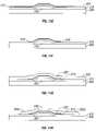
- FIG. 1One interferometric modulator display embodiment comprising an interferometric MEMS display element is illustrated in FIG. 1 .
- the pixelsare in either a bright or dark state.
- the display elementIn the bright (“on” or “open”) state, the display element reflects a large portion of incident visible light to a user.
- the dark (“off” or “closed”) stateWhen in the dark (“off” or “closed”) state, the display element reflects little incident visible light to the user.
- the light reflectance properties of the “on” and “off” statesmay be reversed.
- MEMS pixelscan be configured to reflect predominantly at selected colors, allowing for a color display in addition to black and white.
- FIG. 1is an isometric view depicting two adjacent pixels in a series of pixels of a visual display, wherein each pixel comprises a MEMS interferometric modulator.
- an interferometric modulator displaycomprises a row/column array of these interferometric modulators.
- Each interferometric modulatorincludes a pair of reflective layers positioned at a variable and controllable distance from each other to form a resonant optical gap with at least one variable dimension.
- one of the reflective layersmay be moved between two positions. In the first position, referred to herein as the relaxed position, the movable reflective layer is positioned at a relatively large distance from a fixed partially reflective layer.
- the movable reflective layerIn the second position, referred to herein as the actuated position, the movable reflective layer is positioned more closely adjacent to the partially reflective layer. Incident light that reflects from the two layers interferes constructively or destructively depending on the position of the movable reflective layer, producing either an overall reflective or non-reflective state for each pixel.
- the depicted portion of the pixel array in FIG. 1includes two adjacent interferometric modulators 12 a and 12 b .
- a movable reflective layer 14 ais illustrated in a relaxed position at a predetermined distance from an optical stack 16 a , which includes a partially reflective layer.
- the movable reflective layer 14 bis illustrated in an actuated position adjacent to the optical stack 16 b.
- optical stack 16typically comprise several fused layers, which can include an electrode layer, such as indium tin oxide (ITO), a partially reflective layer, such as chromium, and a transparent dielectric.
- ITOindium tin oxide
- the optical stack 16is thus electrically conductive, partially transparent, and partially reflective, and may be fabricated, for example, by depositing one or more of the above layers onto a transparent substrate 20 .
- the partially reflective layercan be formed from a variety of materials that are partially reflective such as various metals, semiconductors, and dielectrics.
- the partially reflective layercan be formed of one or more layers of materials, and each of the layers can be formed of a single material or a combination of materials.
- the layers of the optical stack 16are patterned into parallel strips, and may form row electrodes in a display device as described further below.
- the movable reflective layers 14 a , 14 bmay be formed as a series of parallel strips of a deposited metal layer or layers (orthogonal to the row electrodes of 16 a , 16 b ) deposited on top of posts 18 and an intervening sacrificial material deposited between the posts 18 . When the sacrificial material is etched away, the movable reflective layers 14 a , 14 b are separated from the optical stacks 16 a , 16 b by a defined gap 19 .
- a highly conductive and reflective materialsuch as aluminum may be used for the reflective layers 14 , and these strips may form column electrodes in a display device.
- the gap 19remains between the movable reflective layer 14 a and optical stack 16 a , with the movable reflective layer 14 a in a mechanically relaxed state, as illustrated by the pixel 12 a in FIG. 1 .
- the capacitor formed at the intersection of the row and column electrodes at the corresponding pixelbecomes charged, and electrostatic forces pull the electrodes together.
- the movable reflective layer 14is deformed and is forced against the optical stack 16 .
- a dielectric layerwithin the optical stack 16 may prevent shorting and control the separation distance between layers 14 and 16 , as illustrated by pixel 12 b on the right in FIG. 1 .
- the behavioris the same regardless of the polarity of the applied potential difference. In this way, row/column actuation that can control the reflective vs. non-reflective pixel states is analogous in many ways to that used in conventional LCD and other display technologies.
- FIGS. 2 through 5Billustrate one exemplary process and system for using an array of interferometric modulators in a display application.
- FIG. 2is a system block diagram illustrating one embodiment of an electronic device that may incorporate aspects of the invention.
- the electronic deviceincludes a processor 21 which may be any general purpose single- or multi-chip microprocessor such as an ARM, Pentium®, Pentium II®, Pentium III®, Pentium IV®, Pentium® Pro, an 8051, a MIPS®, a Power PC®, an ALPHA®, or any special purpose microprocessor such as a digital signal processor, microcontroller, or a programmable gate array.
- the processor 21may be configured to execute one or more software modules.
- the processormay be configured to execute one or more software applications, including a web browser, a telephone application, an email program, or any other software application.
- the processor 21is also configured to communicate with an array driver 22 .
- the array driver 22includes a row driver circuit 24 and a column driver circuit 26 that provide signals to a display array or panel 30 .
- the cross section of the array illustrated in FIG. 1is shown by the lines 1 - 1 in FIG. 2 .
- the row/column actuation protocolmay take advantage of a hysteresis property of these devices illustrated in FIG. 3 . It may require, for example, a 10 volt potential difference to cause a movable layer to deform from the relaxed state to the actuated state. However, when the voltage is reduced from that value, the movable layer maintains its state as the voltage drops back below 10 volts.
- the movable layerdoes not relax completely until the voltage drops below 2 volts.
- a window of applied voltageabout 3 to 7 V in the example illustrated in FIG. 3 , within which the device is stable in either the relaxed or actuated state. This is referred to herein as the “hysteresis window” or “stability window.”
- the row/column actuation protocolcan be designed such that during row strobing, pixels in the strobed row that are to be actuated are exposed to a voltage difference of about 10 volts, and pixels that are to be relaxed are exposed to a voltage difference of close to zero volts.
- each pixelsees a potential difference within the “stability window” of 3-7 volts in this example.
- This featuremakes the pixel design illustrated in FIG. 1 stable under the same applied voltage conditions in either an actuated or relaxed pre-existing state. Since each pixel of the interferometric modulator, whether in the actuated or relaxed state, is essentially a capacitor formed by the fixed and moving reflective layers, this stable state can be held at a voltage within the hysteresis window with almost no power dissipation. Essentially no current flows into the pixel if the applied potential is fixed.
- a display framemay be created by asserting the set of column electrodes in accordance with the desired set of actuated pixels in the first row.
- a row pulseis then applied to the row 1 electrode, actuating the pixels corresponding to the asserted column lines.
- the asserted set of column electrodesis then changed to correspond to the desired set of actuated pixels in the second row.
- a pulseis then applied to the row 2 electrode, actuating the appropriate pixels in row 2 in accordance with the asserted column electrodes.
- the row 1 pixelsare unaffected by the row 2 pulse, and remain in the state they were set to during the row 1 pulse. This may be repeated for the entire series of rows in a sequential fashion to produce the frame.
- the framesare refreshed and/or updated with new display data by continually repeating this process at some desired number of frames per second.
- FIGS. 4 , 5 A, and 5 Billustrate one possible actuation protocol for creating a display frame on the 3 ⁇ 3 array of FIG. 2 .
- FIG. 4illustrates a possible set of column and row voltage levels that may be used for pixels exhibiting the hysteresis curves of FIG. 3 .
- actuating a pixelinvolves setting the appropriate column to ⁇ V bias , and the appropriate row to + ⁇ V, which may correspond to ⁇ 5 volts and +5 volts, respectively. Relaxing the pixel is accomplished by setting the appropriate column to +V bias , and the appropriate row to the same + ⁇ V, producing a zero volt potential difference across the pixel.
- the pixelsare stable in whatever state they were originally in, regardless of whether the column is at +V bias , or ⁇ V bias .
- voltages of opposite polarity than those described abovecan be used, e.g., actuating a pixel can involve setting the appropriate column to +V bias , and the appropriate row to ⁇ V.
- releasing the pixelis accomplished by setting the appropriate column to ⁇ V bias , and the appropriate row to the same ⁇ V, producing a zero volt potential difference across the pixel.
- FIG. 5Bis a timing diagram showing a series of row and column signals applied to the 3 ⁇ 3 array of FIG. 2 which will result in the display arrangement illustrated in FIG. 5A , where actuated pixels are non-reflective.
- the pixelsPrior to writing the frame illustrated in FIG. 5A , the pixels can be in any state, and in this example, all the rows are at 0 volts, and all the columns are at +5 volts. With these applied voltages, all pixels are stable in their existing actuated or relaxed states.
- pixels (1,1), (1,2), (2,2), (3,2) and (3,3)are actuated.
- columns 1 and 2are set to ⁇ 5 volts
- column 3is set to +5 volts. This does not change the state of any pixels, because all the pixels remain in the 3-7 volt stability window.
- Row 1is then strobed with a pulse that goes from 0, up to 5 volts, and back to zero. This actuates the (1,1) and (1,2) pixels and relaxes the (1,3) pixel. No other pixels in the array are affected.
- column 2is set to ⁇ 5 volts
- columns 1 and 3are set to +5 volts.
- Row 3is similarly set by setting columns 2 and 3 to ⁇ 5 volts, and column 1 to +5 volts.
- the row 3 strobesets the row 3 pixels as shown in FIG. 5A .
- the row potentialsare zero, and the column potentials can remain at either +5 or ⁇ 5 volts, and the display is then stable in the arrangement of FIG. 5A . It will be appreciated that the same procedure can be employed for arrays of dozens or hundreds of rows and columns.
- FIGS. 6A and 6Bare system block diagrams illustrating an embodiment of a display device 40 .
- the display device 40can be, for example, a cellular or mobile telephone.
- the same components of display device 40 or slight variations thereofare also illustrative of various types of display devices such as televisions and portable media players.
- the display device 40includes a housing 41 , a display 30 , an antenna 43 , a speaker 45 , an input device 48 , and a microphone 46 .
- the housing 41is generally formed from any of a variety of manufacturing processes as are well known to those of skill in the art, including injection molding and vacuum forming.
- the housing 41may be made from any of a variety of materials, including, but not limited to, plastic, metal, glass, rubber, and ceramic, or a combination thereof.
- the housing 41includes removable portions (not shown) that may be interchanged with other removable portions of different color, or containing different logos, pictures, or symbols.
- the display 30 of exemplary display device 40may be any of a variety of displays, including a bi-stable display, as described herein.
- the display 30includes a flat-panel display, such as plasma, EL, OLED, STN LCD, or TFT LCD as described above, or a non-flat-panel display, such as a CRT or other tube device, as is well known to those of skill in the art.
- the display 30includes an interferometric modulator display, as described herein.
- the components of one embodiment of exemplary display device 40are schematically illustrated in FIG. 6B .
- the illustrated exemplary display device 40includes a housing 41 and can include additional components at least partially enclosed therein.
- the exemplary display device 40includes a network interface 27 that includes an antenna 43 , which is coupled to a transceiver 47 .
- the transceiver 47is connected to a processor 21 , which is connected to conditioning hardware 52 .
- the conditioning hardware 52may be configured to condition a signal (e.g., filter a signal).
- the conditioning hardware 52is connected to a speaker 45 and a microphone 46 .
- the processor 21is also connected to an input device 48 and a driver controller 29 .
- the driver controller 29is coupled to a frame buffer 28 and to an array driver 22 , which in turn is coupled to a display array 30 .
- a power supply 50provides power to all components as required by the particular exemplary display device 40 design.
- the network interface 27includes the antenna 43 and the transceiver 47 so that the exemplary display device 40 can communicate with one or more devices over a network. In one embodiment, the network interface 27 may also have some processing capabilities to relieve requirements of the processor 21 .
- the antenna 43is any antenna known to those of skill in the art for transmitting and receiving signals. In one embodiment, the antenna transmits and receives RE signals according to the IEEE 802.11 standard, including IEEE 802.11(a), (b), or (g). In another embodiment, the antenna transmits and receives RE signals according to the BLUETOOTH standard. In the case of a cellular telephone, the antenna is designed to receive CDMA, GSM, AMPS, or other known signals that are used to communicate within a wireless cell phone network.
- the transceiver 47pre-processes the signals received from the antenna 43 so that they may be received by and further manipulated by the processor 21 .
- the transceiver 47also processes signals received from the processor 21 so that they may be transmitted from the exemplary display device 40 via the antenna 43 .
- the transceiver 47can be replaced by a receiver.
- network interface 27can be replaced by an image source, which can store or generate image data to be sent to the processor 21 .
- the image sourcecan be a digital video disc (DVD) or a hard-disc drive that contains image data, or a software module that generates image data.
- Processor 21generally controls the overall operation of the exemplary display device 40 .
- the processor 21receives data, such as compressed image data from the network interface 27 or an image source, and processes the data into raw image data or into a format that is readily processed into raw image data.
- the processor 21then sends the processed data to the driver controller 29 or to frame buffer 28 for storage.
- Raw datatypically refers to the information that identifies the image characteristics at each location within an image. For example, such image characteristics can include color, saturation, and gray-scale level.
- the processor 21includes a microcontroller, CPU, or logic unit to control operation of the exemplary display device 40 .
- Conditioning hardware 52generally includes amplifiers and filters for transmitting signals to the speaker 45 , and for receiving signals from the microphone 46 .
- Conditioning hardware 52may be discrete components within the exemplary display device 40 , or may be incorporated within the processor 21 or other components.
- the driver controller 29takes the raw image data generated by the processor 21 either directly from the processor 21 or from the frame buffer 28 and reformats the raw image data appropriately for high speed transmission to the array driver 22 . Specifically, the driver controller 29 reformats the raw image data into a data flow having a raster-like format, such that it has a time order suitable for scanning across the display array 30 . Then the driver controller 29 sends the formatted information to the array driver 22 .
- a driver controller 29such as a LCD controller, is often associated with the system processor 21 as a stand-alone Integrated Circuit (IC), such controllers may be implemented in many ways. They may be embedded in the processor 21 as hardware, embedded in the processor 21 as software, or fully integrated in hardware with the array driver 22 .
- the array driver 22receives the formatted information from the driver controller 29 and reformats the video data into a parallel set of waveforms that are applied many times per second to the hundreds and sometimes thousands of leads coming from the display's x-y matrix of pixels.
- driver controller 29is a conventional display controller or a bi-stable display controller (e.g., an interferometric modulator controller).
- array driver 22is a conventional driver or a bi-stable display driver (e.g., an interferometric modulator display).
- a driver controller 29is integrated with the array driver 22 .
- display array 30is a typical display array or a bi-stable display array (e.g., a display including an array of interferometric modulators).
- the input device 48allows a user to control the operation of the exemplary display device 40 .
- input device 48includes a keypad, such as a QWERTY keyboard or a telephone keypad, a button, a switch, a touch-sensitive screen, or a pressure- or heat-sensitive membrane.
- the microphone 46is an input device for the exemplary display device 40 . When the microphone 46 is used to input data to the device, voice commands may be provided by a user for controlling operations of the exemplary display device 40 .
- Power supply 50can include a variety of energy storage devices as are well known in the art.
- power supply 50is a rechargeable battery, such as a nickel-cadmium battery or a lithium ion battery.
- power supply 50is a renewable energy source, a capacitor, or a solar cell including a plastic solar cell, and solar-cell paint.
- power supply 50is configured to receive power from a wall outlet.
- control programmabilityresides, as described above, in a driver controller which can be located in several places in the electronic display system. In some embodiments, control programmability resides in the array driver 22 . Those of skill in the art will recognize that the above-described optimizations may be implemented in any number of hardware and/or software components and in various configurations.
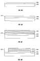
- FIGS. 7A-7Eillustrate five different embodiments of the movable reflective layer 14 and its supporting structures.
- FIG. 7Ais a cross section of the embodiment of FIG. 1 , where a strip of metal material 14 is deposited on orthogonally extending supports 18 .
- FIG. 7Bthe moveable reflective layer 14 is attached to supports at the corners only, on tethers 32 .
- FIG. 7Cthe moveable reflective layer 14 is suspended from a deformable layer 34 , which may comprise a flexible metal.
- the deformable layer 34connects, directly or indirectly, to the substrate 20 around the perimeter of the deformable layer 34 .
- connection postsare herein referred to as support posts.
- the embodiment illustrated in FIG. 7Dhas support post plugs 42 upon which the deformable layer 34 rests.
- the movable reflective layer 14remains suspended over the gap, as in FIGS. 7A-7C , but the deformable layer 34 does not form the support posts by filling holes between the deformable layer 34 and the optical stack 16 . Rather, the support posts are formed of a planarization material, which is used to form support post plugs 42 .
- the embodiment illustrated in FIG. 7Eis based on the embodiment shown in FIG. 7D , but may also be adapted to work with any of the embodiments illustrated in FIGS. 7A-7C , as well as additional embodiments not shown. In the embodiment shown in FIG. 7E , an extra layer of metal or other conductive material has been used to form a bus structure 44 . This allows signal routing along the back of the interferometric modulators, eliminating a number of electrodes that may otherwise have had to be formed on the substrate 20 .
- the interferometric modulatorsfunction as direct-view devices, in which images are viewed from the front side of the transparent substrate 20 , the side opposite to that upon which the modulator is arranged.
- the reflective layer 14optically shields the portions of the interferometric modulator on the side of the reflective layer opposite the substrate 20 , including the deformable layer 34 . This allows the shielded areas to be configured and operated upon without negatively affecting the image quality.
- Such shieldingallows the bus structure 44 in FIG. 7E , which provides the ability to separate the optical properties of the modulator from the electromechanical properties of the modulator, such as addressing and the movements that result from that addressing.
- This separable modulator architectureallows the structural design and materials used for the electromechanical aspects and the optical aspects of the modulator to be selected and to function independently of each other.
- the embodiments shown in FIGS. 7C-7Ehave additional benefits deriving from the decoupling of the optical properties of the reflective layer 14 from its mechanical properties, which are carried out by the deformable layer 34 .
- Thisallows the structural design and materials used for the reflective layer 14 to be optimized with respect to the optical properties, and the structural design and materials used for the deformable layer 34 to be optimized with respect to desired mechanical properties.
- Active-matrix elementscan be used to supply voltages and thereby control the optical state of an interferometric modulator.
- the active-matrix elementsrequire less power consumption than comparable passive-matrix elements. While an active-matrix element may be positioned adjacent to an interferometric modulator, this would result in a decrease in the pixel aperture ratio and may reduce the brightness or the number of grey levels that can be provided by the device. However, by positioning an active-matrix element behind an interferometric modulator with respect to incident light, the active-matrix element may cause minimal to no decrease in the optical aperture ratio and the device may therefore continue to provide enough brightness or the number of grey levels.
- interferometric modulators and active-matrix elementsare formed separately and then appropriately positioned relative to each other. Illustrative methods of separately forming an interferometric modulator and an active-matrix element are described below in FIGS. 8 through 11 .
- FIGS. 12 and 13describe devices in which active-matrix elements are positioned behind interferometric modulators with respect to incident light, in which both the active-matrix element and the interferometric modulators may be separately formed on two substrates.
- FIGS. 14 through 20describe other embodiments in which one or more components of an interferometric modulator and one or more components of an active matrix may be formed on the same substrate.
- FIG. 8is a flow diagram illustrating certain steps in an embodiment of a method of making a MEMS device. Such steps may be present in a process for manufacturing, e.g., interferometric modulators of the general type illustrated in FIGS. 1 and 7 , along with other steps not shown in FIG. 8 .
- FIGS. 9A through 9Gschematically illustrate an embodiment of a method for fabricating a MEMS device using conventional semiconductor manufacturing techniques such as photolithography, deposition, masking, etching (e.g., dry methods such as plasma etch and wet methods), etc.
- Depositionmay include “dry” methods such as chemical vapor deposition (CVD, including plasma-enhanced CVD and thermal CVD) and sputter coating, and wet methods such as spin coating.
- CVDchemical vapor deposition
- thermal CVDthermal CVD
- wet methodssuch as spin coating.
- the process 800begins at step 805 with the formation of an electrically conductive layer 905 over an interferometric modulator (iMoD) substrate 900 .
- the iMoD substrate 900may be a transparent substrate such as glass or plastic and may have been subjected to prior preparation step(s), e.g., cleaning, to facilitate efficient formation of the electrically conductive layer 905 .
- the electrically conductive layer 905can be a single layer structure or a multiple sub-layer structure as described above.
- the layer 905is formed by deposition of an electrically conductive material on the iMoD substrate 900 .
- the electrically conductive layer 905may be formed into electrodes through subsequent patterning and etching not shown in FIG. 8 or 9 .
- the electrically conductive layer 905may be a metal or a semiconductor (such as silicon) doped to have the desired conductivity.
- the electrically conductive layer 905is a multilayer structure comprising a transparent conductor (such as indium tin oxide) or partially reflective layer (such as chromium).
- the process 800continues at step 810 with the formation of a dielectric layer 910 over at least a portion of the electrically conductive layer 905 as shown in FIG. 9B .
- the dielectric layer 910may comprise insulating materials such as silicon oxide and/or aluminum oxide.
- the dielectric layer 910serves to insulate the first electrically conductive layer 905 from an electrically conductive movable layer (such as movable layer 14 of FIGS. 1 and 7 ) in an interferometric modulator.
- the dielectric layer 910may be formed by known deposition methods, such as CVD.
- the optical stack 16 of the resulting deviceincludes both the electrically conductive layer 905 and the dielectric layer 910 .
- the process 800continues at step 815 with the formation of a sacrificial layer 915 as shown in FIG. 9C .
- the sacrificial layer 915may comprise a material etchable by XeF 2 , such as molybdenum or amorphous silicon. Deposition methods such as sputtering, evaporation, or CVD (thermal or plasma enhanced) may be used in forming the sacrificial layer 915 .
- the sacrificial layer 915can be patterned and etched to form one or more support structure apertures 920 , as shown in FIG. 9D . In the embodiment shown in FIG.
- the support structure apertures 920extend entirely through the first sacrificial layer 915 and the dielectric layer 910 to the first electrically conductive layer 905 .
- support structures 925are formed, which in some embodiments can comprise depositing support material into the apertures 920 from FIG. 9D .
- the support structures 925may comprise a non-conductive material.
- the process 800continues at step 825 with the formation of a second electrically conductive layer 930 over the sacrificial layer 915 and, in the illustrated embodiment, over the support structures 925 , as shown in FIG. 9F .
- the second electrically conductive layerwill comprise a movable layer such as the movable layer 14 of an interferometric modulator as shown in FIGS. 1 and 7 . Since the sacrificial layer 915 is still present at this stage of the process 800 , the movable layer is typically not yet movable.
- a partially fabricated MEMS devicee.g.
- the second electrically conductive layer 930may comprise a metal (e.g. aluminum or aluminum alloy). In some embodiments, the second electrically conductive layer 930 comprises aluminum. Forming the electrically conductive layer 930 in step 850 may include one or more deposition steps as well as one or more patterning or masking steps.
- the process 800continues at step 830 where the sacrificial layer 915 is removed (e.g., by etching) as shown in FIG. 9G .
- One or more support structures 925can support the second electrically conductive layer 930 , thereby forming a gap or a cavity 935 .
- the cavity 935is formed between the dielectric layer 910 and the second electrically conductive layer 930 as illustrated in FIG. 9G . Since the sacrificial layer is removed during step 830 of the process 800 , the second electrically conductive layer 930 is typically movable after this stage. After removal of the sacrificial material, the resulting fully or partially fabricated interferometric modulator may be referred to herein as a “released” interferometric modulator.
- the MEMS deviceis controlled by a control element.
- the control elementmay comprise one or more of an electronic switching element and a transistor.
- the control elementmay be an active matrix element, which may comprise one or more of a transistor (e.g., a thin-film transistor), a diode, a MEMS switch, and may further comprise, a semiconductor film comprising one or more of amorphous silicon, polycrystalline silicon, and CdSe. Active matrix elements may be formed by a variety of methods and are not limited to those described herein.
- FIG. 10is a flow diagram illustrating certain steps in an embodiment of a method of making an active matrix element. Such steps may be present in a process for manufacturing, along with other steps not shown in FIG. 10 .
- FIGS. 11A through 11Jschematically illustrate an embodiment of a method for fabricating an active matrix element using conventional semiconductor manufacturing techniques such as photolithography, deposition, masking, etching (e.g., dry methods such as plasma etch and wet methods), etc.
- Depositionmay include “dry” methods such as chemical vapor deposition (CVD, including plasma-enhanced CVD and thermal CVD) and sputter coating, and wet methods such as spin coating.
- CVDchemical vapor deposition
- thermal CVDthermal CVD
- wet methodssuch as spin coating.
- the process 100begins at step 105 with the formation of a metal layer 205 over an active matrix (AM) substrate 200 .
- the AM substrate 200may comprise silicon.
- the metal layer 205may comprises one or more of chromium, molybdenum, aluminum, and an aluminum alloy. As shown in FIG. 11B , a portion of the metal layer 205 can be removed using, for example, a photolithography technique and an etching technique.
- the process 100continues at step 110 with the formation of a dielectric layer 210 over the metal layer 205 as shown in FIG. 11C .
- the dielectric layer 210may comprise insulating materials such as amorphous silicon nitride (SiN x ), silicon oxynitride, nitrogen doped silicon oxide and/or another dielectric material.
- the process 100continues at step 115 with the formation of an active layer 215 as shown in FIG. 11D .
- the active layer 215comprises amorphous silicon.
- the active layer 215 and the dielectric layer 210are deposited together. One or both of these layers can be deposited by, for example, plasma-enhanced chemical vapor deposition.
- the process 100continues at step 120 with the formation of an ohmic contact layer 220 as shown in FIG. 11E .
- the ohmic contact layer 220comprises phosphorus-doped (or n+ doped) amorphous silicon.
- the ohmic contact layer 220comprises n+ doped amorphous silicon.
- a portion of the active layer 215 and the ohmic contact layer 220can be removed using, for example, a photolithography technique and an etch technique, thereby forming a thin-film transistor island, comprising metal layer 205 , a portion of dielectric layer 210 , active layer 215 , and ohmic contact layer 220 .
- the process 100continues at step 125 with the formation of a second metal layer 225 as shown in FIG. 11G .
- the second metal layer 225may comprise, for example, molybdenum, aluminum, or chromium.
- a portion of the second metal layer 225can be removed using, for example, a photolithography and a dry-etch technique.
- the photolithographycan divide the second metal layer 225 into two portions forming a gap 230 in between and thereby forming a drain electrode 225 a and a source electrode 225 b.
- the process 100continues with optional step 130 with the formation of a second dielectric layer 235 as shown in FIG. 11I .
- the second dielectric layer 235may comprise amorphous silicon nitride or amorphous silicon oxide.
- the process 100continues at step 135 with the formation of a passivation layer 240 as shown in FIG. 11J .
- the passivation layer 240may comprise passivation and/or planarization materials such as polyimide, polyamide, acrylic, or BCB (benzocyclobutane).
- the resulting structurecomprising the metal layer 205 , dielectric layer 210 , active layer 215 , ohmic contact layer 220 , drain electrode 225 a , source electrode 225 b , second dielectric layer 235 and passivation layer 240 is one example of what will be referred to herein as an active matrix element 250 .
- an interferometric devicecomprises an interferometric modulator (iMoD) and at least one control element coupled to the iMoD, the at least one control element located behind the at least one iMoD with respect to incident light.
- FIG. 12presents an overview of one method for forming such a device.
- the relative positioning of the components of the devicemay maximize the optical aperture of the iMoD. For example, by constructing the AM element behind the iMoD with respect to the viewer of the iMoD, no or minimal aperture is lost from the iMoD because of the AM element. This is contrary to some possible implementations where the AM element is formed on the same plane as the iMoD and thus takes up some of the available iMoD aperture that could be used for display applications, for example.
- FIG. 12is a flow diagram illustrating certain steps in an embodiment of a method of making a MEMS device including an iMoD and a control element coupled to the iMoD. Such steps may be present in a process for manufacturing, along with other steps not shown in FIG. 12 .
- FIG. 12presents an embodiment in which iMoD devices are formed on a first substrate, AM elements are formed on a second substrate, and the first substrate is attached mechanically and electrically to the second substrate so as to form the final device.
- the process 300begins at step 305 with the providing of a first substrate.
- the first substratemay be a transparent substrate such as glass or plastic and may have been subjected to prior preparation step(s), e.g., cleaning.
- the process 300continues at step 310 with the forming of an interferometric display device.
- the forming of an interferometric display devicecan comprise the process illustrated in FIG. 9 .
- the forming of an interferometric display devicecan comprise only some of the steps of process illustrated in FIG. 9 .
- the forming of an interferometric display devicemay comprise forming all components of the interferometric display device over the first substrate, or alternatively may comprise forming only some of the components of the interferometric display device over the first substrate.
- the process 300continues at step 315 with the providing of a second substrate.
- the second substratemay comprise silicon.
- the process 300continues at step 320 with the forming of an active matrix element.
- the forming of an active matrix elementcan comprise process 100 .
- the forming of an active matrix elementcan comprise only some of the steps of process 100 .
- the forming of an active matrix elementmay comprise forming all components of the active matrix element over the second substrate, or alternatively may comprise forming only some of the components of the active matrix element over the second substrate.
- the process 300continues at step 325 with the attaching the first substrate to the second substrate.
- the substratesmay be attached using one or more of supports, spring-loaded electrodes, conductive epoxy glue, and supports comprising flexible components.
- Supports comprising flexible componentsmay include a tension member to ensure solid contact between layers separated by the support.
- the substratesmay be attached such that the active matrix element is positioned behind the interferometric display device with respect to incident light.
- some of the components of the active matrix elementmay be formed over the first substrate and other active matrix element components over the second substrate.
- some of the components of the interferometric display devicemay be formed over the first substrate and other interferometric display device components may be formed over the second substrate.
- FIG. 13illustrates various configurations for iMoDs coupled to control elements, allowing for separate formation of the iMoDs and the control elements.
- the iMoDs and control elementsmay be directly or indirectly connected by supports. All configurations include an active matrix element behind an interferometric modulator with respect to incident light. It will be understood that the devices shown in FIG. 13 may be formed by other methods in which the control element and the iMoD are not separately formed.
- an iMoDis formed over an iMoD substrate 900 .
- the iMoDmay comprise an electrically conductive layer 905 and a second electrically conductive layer 930 , which may be a movable electrode.
- the iMoDmay further include a dielectric layer 910 , one or more support structures 925 , and/or a cavity 935 .
- the iMoDis formed on the iMoD substrate 900 by the process illustrated in FIG. 9 .
- An active matrix element 250may be formed on an AM substrate 200 . While the active matrix element 250 may be the same as that indicated in FIG.
- An electrical connection 410may connect the active matrix element 250 to the second electrically conductive layer 930 of the iMoD.
- the electrical connection 410may, for example, connect a source electrode 225 b (not shown in FIG. 13 for the sake of clarity) of the active matrix element 250 to the second electrically conductive layer 930 .
- the electrical connection 410may comprise a metal, which may be nickel.
- the devicemay further comprise one or more second supports, which may comprise flexible components.
- the one or more second supportsmay include one or more short supports 405 that are positioned between the second electrically conductive layer 930 and the AM substrate 200 , as, for example, illustrated in FIG. 13A .
- the one or more second supportsmay include one or more long supports 415 that are positioned between the AM substrate 200 and the iMoD substrate 900 , as, for example, illustrated in FIG. 13B .
- the second electrically conductive layer 930 of the iMoDis not supported by the one or more support structures 925 .
- the second electrically conductive layer 930may be connected to a spring hanger 425 .
- the spring hanger 425may also comprise an electrically conductive material.
- the spring hanger 425may be connected to the active matrix element 250 by one or more electrically-conductive supports 420 .
- the iMoDmay be connected to the active matrix element by a support with a flexible component formed either over the iMoD substrate 900 or over the AM substrate 200 .
- Spring-loaded electrodesmay provide strong electrical connections
- components of an interferometric modulatorare formed on one substrate, and components of an active matrix element are formed on another substrate.
- an interferometric modulator and/or an active matrix elementmay not be fully formed on either substrate, but when the two substrates are directly or indirectly attached mechanically and electrically to each other, the device comprises both a fully-formed interferometric modulator and an active matrix element.
- a potential advantage of such arrangementis a reduction in processing steps needed to fabricate the final interferometric modulator device and controlling AM element.
- FIG. 14is a flow diagram illustrating certain steps in an embodiment of a method of making a MEMS device. Such steps may be present in a process for manufacturing, along with other steps not shown in FIG. 14 .
- FIGS. 15A through 15Qschematically illustrate an embodiment of a method for fabricating a MEMS device using conventional semiconductor manufacturing techniques such as photolithography, deposition, masking, etching (e.g., dry methods such as plasma etch and wet methods), etc.
- Depositionmay include “dry” methods such as chemical vapor deposition (CVD, including plasma-enhanced CVD and thermal CVD) and sputter coating, and wet methods such as spin coating.
- CVDchemical vapor deposition
- thermal CVDthermal CVD
- wet methodssuch as spin coating.
- the process 500begins at step 505 with the providing of an active matrix (AM) substrate 200 .
- the AM substrate 200may comprise one or more of a glass substrate, a flexible/plastic substrate, and a silicon substrate with a coated insulator such as silicon oxide or silicon nitride.
- the process 500continues at step 510 with the formation of an active matrix element 250 on the AM substrate 200 , as shown in FIG. 15A . While the active matrix element 250 may be the same as that indicated in FIG. 11 and may be formed by process 100 , because there are several methods and structures may be used, active matrix element 250 need not be formed by process 100 and need not be the active matrix element illustrated in FIG. 11 .
- the process 500continues at step 515 with the formation of a first sacrificial layer 605 , which may be formed over the active matrix element 250 , as shown in FIG. 15B .
- the first sacrificial layer 605may comprise a material etchable by XeF 2 , such as molybdenum or amorphous silicon. Deposition methods such as CVD, sputtering or spin coating may be used in forming the first sacrificial layer 605 .
- the first sacrificial layer 605can be patterned and etched to form one or more first support structure apertures 610 , as shown in FIG. 15C .
- the process 500continues at step 520 with the formation of one or more first support structures 615 , which, in some embodiments, can comprise depositing support material into the first apertures 610 shown in FIG. 15D .
- the one or more first support structures 615may comprise a non-conductive material.
- the first sacrificial layer 605can again be patterned and etched to form an electrical connection aperture 620 , as shown in FIG. 15E .
- the process 500continues at step 525 with the formation of an electrical connection layer 625 , as shown in FIG. 15F .
- the electrical connection layer 625may be formed above the one or more first support structures 615 and/or above the first sacrificial layer 605 .
- the electrical connection layermay comprise a metal, which may be, for example, nickel.
- the electrical connection layer 625can be patterned and etched, such that, for example, the electrical connection layer does not extend past the support structures 615 , as shown in FIG. 15G .
- the process 500continues at step 530 with the formation of a movable electrode 630 , as shown in FIG. 15H .
- the movable electrode 630may comprise an electrically conductive material.
- the moveable electrode 630may be formed on the electrical connection layer 625 .
- the movable electrode 630can be patterned and etched, such that, for example, the electrical connection layer does not extend past the support structures 615 , as shown in FIG. 15I .
- the process 535continues at step 530 with the formation of a second sacrificial layer 635 , which may be formed over the movable electrode 630 , as shown in FIG. 15J .
- the second sacrificial layer 635may comprise a material etchable by XeF 2 , such as molybdenum or amorphous silicon.
- the second sacrificial layer 635can be patterned and etched to form one or more second support structure apertures 640 , as shown in FIG. 15K .
- the process 500continues at step 540 with the formation of one or more second support structures 645 , which, in some embodiments, can comprise depositing support material into the apertures 640 shown in FIG. 15K .
- the one or more second support structures 645may comprise a non-conductive material.
- the first sacrificial layer 605 and/or the second sacrificial layer 635may be removed (e.g., by etching) as shown in FIG. 15M . Both sacrificial layers 605 and 635 may be removed simultaneously.
- the first support structures 615can support the second electrically conductive layer 930 , thereby forming a first cavity 650 .
- the cavity 650is formed between the active matrix element 250 and the electrical connection layer 625 .
- the cavity 650is formed between the active matrix element 250 and the movable electrode 630 .
- an active matrix elementhas been formed (e.g. on a non-transparent silicon substrate) and an iMoD has been partially formed atop the AM element.
- the process 500continues at step 545 with the providing of an iMoD substrate 900 .
- the iMoD substrate 900may be a transparent substrate such as glass or plastic and may have been subjected to prior preparation step(s), e.g., cleaning.
- a planarization layer 655is formed on the iMoD substrate 900 .
- the planarization layer 655may comprise one or more color filters to modify a color of light reflected from the iMoD and/or black masks.
- the process 500continues at step 555 with the formation of an electrode layer 905 , as shown in FIG. 15O .
- the electrode layer 905may comprise a transparent conductive material, such as, for example, indium tin oxide (ITO).
- ITOindium tin oxide
- the electrode layer 905may be formed on the planarization layer 655 .
- the process 500continues at step 560 with the formation of an optical layer 910 , as shown in FIG. 15P .
- the optical layer 910may be a dielectric layer such as an oxide, formed on or over the electrode layer 905 .
- the process 500continues at step 555 with mechanical and electrical attachment of the AM substrate 200 to the iMoD substrate 900 , as shown in FIG. 15Q .
- the attachmentcan be an indirect attachment.
- the second support structures attached to the AM substrate 200may be attached to the optical layer 910 attached to the iMoD substrate 900 .
- Any suitable meansmay be used to attach the substrates.
- componentsare attached using, for example, epoxy glue which may be electrically conductive.
- FIG. 16illustrates an alternative process for manufacturing a MEMS device comprising an interferometric modulator and an active matrix element. Initially, the device may be formed as illustrated in FIG. 15A-15I . The first sacrificial layer 605 may then be removed (e.g., by etching) as shown in FIG. 16A . A third sacrificial layer 705 may be formed over the movable electrode 630 , as shown in FIG. 16B .
- the third sacrificial layer 705can be patterned and etched to form one or more third support structure apertures 710 , as shown in FIG. 16C .
- One or more third support structures 720are formed, which, in some embodiments, can comprise depositing support material into the apertures 710 shown in FIG. 16D .
- the one or more third structures 720may comprise a non-conductive material.
- the third sacrificial layer 705may be removed (e.g., by etching) as shown in FIG. 16E .
- the resulting componentmay then be attached to the iMoD device component of FIG. 15P , as shown in FIG. 16F . Any suitable means may be used to attach the substrates. In some embodiments, components are attached using, for example, epoxy glue.
- Embodiments shown in FIGS. 13 , 15 and 16include devices in which the active matrix elements are connected to the movable electrode of the iMoD and in which the active matrix elements and the non-movable electrodes of the iMoDs are on opposite sides of the movable electrodes of the iMoDs.
- other embodimentsinclude devices in which the active matrix element is connected to the non-movable electrode of the iMoD.
- the active matrix elements and the interferometric modulators of these devicesmay be formed over the same substrate, which may reduce manufacturing steps.
- FIG. 17refers to an embodiment in which active matrix elements and non-movable electrodes are positioned on the same side of the movable electrodes.
- the process 800begins at step 805 with the providing of a first substrate.
- the first substrateis an AM substrate 200 .
- an active matrix element 250is formed over the AM substrate 200 .
- an electrode layer 910is formed over the active matrix element 250 .
- the electrode layer 910is not a common electrode to multiple iMoD pixels.
- a dielectric layer 910is formed on the electrode layer 910 .
- a sacrificial layer 935is formed over the dielectric layer 910 .
- the sacrificial layer 935can be patterned and etched to form one or more support structure apertures and possibly an indentation for the formation of a movable electrode 930 .
- supportsare formed in the one or more support structure apertures.
- the movable electrode 930is formed over the sacrificial layer 935 .
- a second dielectric layer 1000is formed over the movable electrode 930 .
- the dielectric layer 1000may be transparent. In some embodiments, an additional sacrificial layer is formed over the dielectric layer.
- the sacrificial layercan be patterned and etch to form a spring aperture.
- the second dielectric layer 1000may also be etched to form a spring aperture.
- a mechanical spring/common electrode 1100is formed, which may provide a voltage to the movable electrode 930 .
- the mechanical spring/common electrode 1100may comprise nickel and/or aluminum.
- the mechanical spring/common electrode 1100may extend across multiple pixels.
- the AM substrate 200is attached to a second substrate 1050 . Additional supports may be formed between the AM substrate 200 and the second substrate 1050 in order to attach the substrates.
- FIGS. 18A and 18Bshow two MEMS devices in which both the active matrix element 250 and the electrode layer 910 are positioned on the same side of the movable electrode 930 .
- the devicesmay be made by process 800 .
- the bottom electrically conductive layer 905is not shared across pixels, whereas the mechanical spring/common electrode 1100 does extend across pixels.
- incident lightmay enter the device through the second substrate 1050 .
- the mechanical spring/common electrode 1100is a single layer connected to the movable electrode 930 .
- the mechanical spring/common electrode 1100is discontinuous, contacting the movable electrode 930 on each side of the movable electrode 930 .
- the device of FIG. 18Bmay provide the advantage of allowing for more light reflection than the device of FIG. 18A .
- the iMoDsare built in reverse order to that described in FIGS. 8 and 9 .
- An active matrix elementmay be built over an iMoD, or an iMoD may be built over an active matrix element.
- a second encapsulation substrate 1050may be positioned over the iMoD formed over the AM substrate 200 . Incident light may enter through the second substrate 1050 , such that the iMoD and active matrix element are behind the second substrate 1050 with respect to incident light.
- active matrix elementsmay be formed over an iMoD over a single substrate.
- This embodimentmay provide advantages over embodiments in which active matrix elements and iMoDs are separately formed. For example, these embodiments can provide strong electrical contact between the active matrix elements and the iMoD.
- the process 1100begins at step 1105 with the providing of a first substrate.
- the first substratemay be an iMoD substrate 900 .
- an iMoD 950is formed.
- the iMoD 950may be formed over the iMoD substrate 900 .
- the sacrificial layer 916 of the iMoD 950has not been removed, as shown in FIG. 20A .
- An electrode gap 1205may be formed in the movable electrode 930 of the iMoD 950 , as shown in FIG. 20B .
- a second sacrificial layer 1210is formed over the iMoD 950 , as shown in FIG. 20C .
- the second sacrificial layer 1210may comprise the same materials as the sacrificial layer 915 of the iMoD 950 .
- one or more first vias 1215may be formed in the second sacrificial layer 1210 , as shown in FIG. 20D .
- a planarization layer 1220may be formed over the second sacrificial layer 1210 , as shown in FIG. 20E .
- the planarization layer 1220may comprise a polymer with a low dielectric, such as polyimide, acrylic, or BCB (benzocyclobutene).
- the planarization layer 1220may fill the one or more first vias 1215 .
- a second via 1230is formed, as shown in FIG. 20F .
- the second via 1230may be in the planarization layer 1220 and may end at the movable second electrode 930 .
- one or more planarization gaps 1225may be formed in the planarization layer.
- the planarization gaps 1225 and/or the electrode gap 1205may allow an etchant to remove the sacrificial layer 915 of the iMoD 950 and the second sacrificial layer 1210 .
- the sacrificial layer 915 and the second sacrificial layer 1210are removed to form the iMoD cavity 935 and a second cavity 1235 , as shown in FIG. 20G .
- the sacrificial layers 915 and 1210can be removed after the active matrix element 250 is formed.
- an active matrix elementis formed, as shown in FIG. 20H .
- the active matrix elementmay be formed over the planarization layer 1220 .
- the active matrix element 250may not comprise the passivation layer 240 .
- a component of the active matrix elementextends into the second via 1230 to form an electrical connection with the iMoD 950 .
- a source electrode 225 b of the active matrix element 250may contact the movable electrode 930 of the iMoD 950 .
- an encapsulation substrateis formed over the active matrix element 250 .
- a device formed by process 1100provides strong electrical contact between the active matrix element and the iMoD.
Landscapes
- Physics & Mathematics (AREA)
- Spectroscopy & Molecular Physics (AREA)
- General Physics & Mathematics (AREA)
- Optics & Photonics (AREA)
- Mechanical Light Control Or Optical Switches (AREA)
Abstract
Description
Claims (37)
Priority Applications (1)
| Application Number | Priority Date | Filing Date | Title |
|---|---|---|---|
| US11/765,276US7643199B2 (en) | 2007-06-19 | 2007-06-19 | High aperture-ratio top-reflective AM-iMod displays |
Applications Claiming Priority (1)
| Application Number | Priority Date | Filing Date | Title |
|---|---|---|---|
| US11/765,276US7643199B2 (en) | 2007-06-19 | 2007-06-19 | High aperture-ratio top-reflective AM-iMod displays |
Publications (2)
| Publication Number | Publication Date |
|---|---|
| US20080316566A1 US20080316566A1 (en) | 2008-12-25 |
| US7643199B2true US7643199B2 (en) | 2010-01-05 |
Family
ID=40136175
Family Applications (1)
| Application Number | Title | Priority Date | Filing Date |
|---|---|---|---|
| US11/765,276Expired - Fee RelatedUS7643199B2 (en) | 2007-06-19 | 2007-06-19 | High aperture-ratio top-reflective AM-iMod displays |
Country Status (1)
| Country | Link |
|---|---|
| US (1) | US7643199B2 (en) |
Cited By (29)
| Publication number | Priority date | Publication date | Assignee | Title |
|---|---|---|---|---|
| US20090078316A1 (en)* | 2007-09-24 | 2009-03-26 | Qualcomm Incorporated | Interferometric photovoltaic cell |
| US20090101192A1 (en)* | 2007-10-19 | 2009-04-23 | Qualcomm Incorporated | Photovoltaic devices with integrated color interferometric film stacks |
| US20090126777A1 (en)* | 2007-11-16 | 2009-05-21 | Qualcomm Mems Technologies, Inc. | Simultaneous light collection and illumination on an active display |
| US20090159123A1 (en)* | 2007-12-21 | 2009-06-25 | Qualcomm Mems Technologies, Inc. | Multijunction photovoltaic cells |
| US20090293955A1 (en)* | 2007-11-07 | 2009-12-03 | Qualcomm Incorporated | Photovoltaics with interferometric masks |
| US20090323166A1 (en)* | 2008-06-25 | 2009-12-31 | Qualcomm Mems Technologies, Inc. | Backlight displays |
| US20100053148A1 (en)* | 2008-09-02 | 2010-03-04 | Qualcomm Mems Technologies, Inc. | Light turning device with prismatic light turning features |
| US20100085625A1 (en)* | 2007-07-02 | 2010-04-08 | Qualcomm Mems Technologies, Inc. | Electromechanical device with optical function separated from mechanical and electrical function |
| US20100096011A1 (en)* | 2008-10-16 | 2010-04-22 | Qualcomm Mems Technologies, Inc. | High efficiency interferometric color filters for photovoltaic modules |
| US20100096006A1 (en)* | 2008-10-16 | 2010-04-22 | Qualcomm Mems Technologies, Inc. | Monolithic imod color enhanced photovoltaic cell |
| US20100284055A1 (en)* | 2007-10-19 | 2010-11-11 | Qualcomm Mems Technologies, Inc. | Display with integrated photovoltaic device |
| US20100302803A1 (en)* | 2009-05-29 | 2010-12-02 | Qualcomm Mems Technologies, Inc. | Illumination devices and methods of fabrication thereof |
| US20100309572A1 (en)* | 2007-09-14 | 2010-12-09 | Qualcomm Mems Technologies, Inc. | Periodic dimple array |
| US20110026095A1 (en)* | 2007-07-31 | 2011-02-03 | Qualcomm Mems Technologies, Inc. | Devices and methods for enhancing color shift of interferometric modulators |
| US20110075241A1 (en)* | 2009-09-28 | 2011-03-31 | Qualcomm Mems Technologies, Inc. | Interferometric display with interferometric reflector |
| US20110090554A1 (en)* | 2008-07-11 | 2011-04-21 | Qualcomm Mems Technologies, Inc. | Stiction mitigation with integrated mech micro-cantilevers through vertical stress gradient control |
| US20110199350A1 (en)* | 2010-02-12 | 2011-08-18 | Kelce Steven Wilson | Ambient light-compensated reflective display devices and methods related thereto |
| WO2011130718A2 (en) | 2010-04-16 | 2011-10-20 | Flex Lighting Ii, Llc | Front illumination device comprising a film-based lightguide |
| WO2011130715A2 (en) | 2010-04-16 | 2011-10-20 | Flex Lighting Ii, Llc | Illumination device comprising a film-based lightguide |
| US20130162656A1 (en)* | 2011-12-22 | 2013-06-27 | Robert L. Holman | Angled facets for display devices |
| US8659816B2 (en) | 2011-04-25 | 2014-02-25 | Qualcomm Mems Technologies, Inc. | Mechanical layer and methods of making the same |
| US8693084B2 (en) | 2008-03-07 | 2014-04-08 | Qualcomm Mems Technologies, Inc. | Interferometric modulator in transmission mode |
| US8736939B2 (en) | 2011-11-04 | 2014-05-27 | Qualcomm Mems Technologies, Inc. | Matching layer thin-films for an electromechanical systems reflective display device |
| US8797632B2 (en) | 2010-08-17 | 2014-08-05 | Qualcomm Mems Technologies, Inc. | Actuation and calibration of charge neutral electrode of a display device |
| US8817357B2 (en) | 2010-04-09 | 2014-08-26 | Qualcomm Mems Technologies, Inc. | Mechanical layer and methods of forming the same |
| US8964280B2 (en) | 2006-06-30 | 2015-02-24 | Qualcomm Mems Technologies, Inc. | Method of manufacturing MEMS devices providing air gap control |
| US8963159B2 (en) | 2011-04-04 | 2015-02-24 | Qualcomm Mems Technologies, Inc. | Pixel via and methods of forming the same |
| US9057872B2 (en) | 2010-08-31 | 2015-06-16 | Qualcomm Mems Technologies, Inc. | Dielectric enhanced mirror for IMOD display |
| US9134527B2 (en) | 2011-04-04 | 2015-09-15 | Qualcomm Mems Technologies, Inc. | Pixel via and methods of forming the same |
Families Citing this family (19)
| Publication number | Priority date | Publication date | Assignee | Title |
|---|---|---|---|---|
| US7782517B2 (en) | 2007-06-21 | 2010-08-24 | Qualcomm Mems Technologies, Inc. | Infrared and dual mode displays |
| US7847999B2 (en) | 2007-09-14 | 2010-12-07 | Qualcomm Mems Technologies, Inc. | Interferometric modulator display devices |
| EP2203765A1 (en) | 2007-10-23 | 2010-07-07 | Qualcomm Mems Technologies, Inc. | Adjustably transmissive mems-based devices |
| US7715079B2 (en) | 2007-12-07 | 2010-05-11 | Qualcomm Mems Technologies, Inc. | MEMS devices requiring no mechanical support |
| US8164821B2 (en) | 2008-02-22 | 2012-04-24 | Qualcomm Mems Technologies, Inc. | Microelectromechanical device with thermal expansion balancing layer or stiffening layer |
| US7612933B2 (en) | 2008-03-27 | 2009-11-03 | Qualcomm Mems Technologies, Inc. | Microelectromechanical device with spacing layer |
| US7898723B2 (en) | 2008-04-02 | 2011-03-01 | Qualcomm Mems Technologies, Inc. | Microelectromechanical systems display element with photovoltaic structure |
| US7969638B2 (en) | 2008-04-10 | 2011-06-28 | Qualcomm Mems Technologies, Inc. | Device having thin black mask and method of fabricating the same |
| US8023167B2 (en) | 2008-06-25 | 2011-09-20 | Qualcomm Mems Technologies, Inc. | Backlight displays |
| US7746539B2 (en) | 2008-06-25 | 2010-06-29 | Qualcomm Mems Technologies, Inc. | Method for packing a display device and the device obtained thereof |
| JP5151794B2 (en)* | 2008-08-08 | 2013-02-27 | 富士通株式会社 | Optical module, optical module optical control method, optical switch, and optical switch method |
| US7855826B2 (en)* | 2008-08-12 | 2010-12-21 | Qualcomm Mems Technologies, Inc. | Method and apparatus to reduce or eliminate stiction and image retention in interferometric modulator devices |
| US8270056B2 (en) | 2009-03-23 | 2012-09-18 | Qualcomm Mems Technologies, Inc. | Display device with openings between sub-pixels and method of making same |
| US8270062B2 (en) | 2009-09-17 | 2012-09-18 | Qualcomm Mems Technologies, Inc. | Display device with at least one movable stop element |
| US8149496B2 (en)* | 2009-12-22 | 2012-04-03 | Qualcomm Mems Technologies, Inc. | Integrated touch for IMOD displays using back glass |
| US20120274611A1 (en)* | 2011-04-26 | 2012-11-01 | Qualcomm Mems Technologies, Inc. | Thin film transistors (tft) active-matrix imod pixel layout |
| US20130100090A1 (en)* | 2011-10-21 | 2013-04-25 | Qualcomm Mems Technologies, Inc. | Electromechanical systems variable capacitance device |
| US20130335312A1 (en)* | 2012-06-15 | 2013-12-19 | Qualcomm Mems Technologies, Inc. | Integration of thin film switching device with electromechanical systems device |
| CN109148705B (en) | 2018-08-22 | 2020-03-24 | 武汉华星光电技术有限公司 | Preparation method of OLED substrate and OLED substrate |
Citations (167)
| Publication number | Priority date | Publication date | Assignee | Title |
|---|---|---|---|---|
| US3728030A (en) | 1970-06-22 | 1973-04-17 | Cary Instruments | Polarization interferometer |
| US3955190A (en) | 1972-09-11 | 1976-05-04 | Kabushiki Kaisha Suwa Seikosha | Electro-optical digital display |
| US4403248A (en) | 1980-03-04 | 1983-09-06 | U.S. Philips Corporation | Display device with deformable reflective medium |
| US4441791A (en) | 1980-09-02 | 1984-04-10 | Texas Instruments Incorporated | Deformable mirror light modulator |
| US4786128A (en) | 1986-12-02 | 1988-11-22 | Quantum Diagnostics, Ltd. | Device for modulating and reflecting electromagnetic radiation employing electro-optic layer having a variable index of refraction |
| US4859060A (en) | 1985-11-26 | 1989-08-22 | 501 Sharp Kabushiki Kaisha | Variable interferometric device and a process for the production of the same |
| US4954789A (en) | 1989-09-28 | 1990-09-04 | Texas Instruments Incorporated | Spatial light modulator |
| US4956619A (en) | 1988-02-19 | 1990-09-11 | Texas Instruments Incorporated | Spatial light modulator |
| US4982184A (en) | 1989-01-03 | 1991-01-01 | General Electric Company | Electrocrystallochromic display and element |
| US5022745A (en) | 1989-09-07 | 1991-06-11 | Massachusetts Institute Of Technology | Electrostatically deformable single crystal dielectrically coated mirror |
| US5028939A (en) | 1988-08-23 | 1991-07-02 | Texas Instruments Incorporated | Spatial light modulator system |
| US5091983A (en) | 1987-06-04 | 1992-02-25 | Walter Lukosz | Optical modulation apparatus and measurement method |
| US5096279A (en) | 1984-08-31 | 1992-03-17 | Texas Instruments Incorporated | Spatial light modulator and method |
| US5315370A (en) | 1991-10-23 | 1994-05-24 | Bulow Jeffrey A | Interferometric modulator for optical signal processing |
| US5381232A (en) | 1992-05-19 | 1995-01-10 | Akzo Nobel N.V. | Fabry-perot with device mirrors including a dielectric coating outside the resonant cavity |
| US5471341A (en) | 1991-07-17 | 1995-11-28 | Optron Systems, Inc. | Membrane light modulating systems |
| US5526172A (en) | 1993-07-27 | 1996-06-11 | Texas Instruments Incorporated | Microminiature, monolithic, variable electrical signal processor and apparatus including same |
| US5559358A (en) | 1993-05-25 | 1996-09-24 | Honeywell Inc. | Opto-electro-mechanical device or filter, process for making, and sensors made therefrom |
| US5636052A (en) | 1994-07-29 | 1997-06-03 | Lucent Technologies Inc. | Direct view display based on a micromechanical modulation |
| US5646729A (en) | 1993-01-13 | 1997-07-08 | Vaisala Oy | Single-channel gas concentration measurement method and apparatus using a short-resonator Fabry-Perot interferometer |
| US5646768A (en) | 1994-07-29 | 1997-07-08 | Texas Instruments Incorporated | Support posts for micro-mechanical devices |
| US5661592A (en) | 1995-06-07 | 1997-08-26 | Silicon Light Machines | Method of making and an apparatus for a flat diffraction grating light valve |
| US5665997A (en) | 1994-03-31 | 1997-09-09 | Texas Instruments Incorporated | Grated landing area to eliminate sticking of micro-mechanical devices |
| US5710656A (en) | 1996-07-30 | 1998-01-20 | Lucent Technologies Inc. | Micromechanical optical modulator having a reduced-mass composite membrane |
| US5786927A (en) | 1997-03-12 | 1998-07-28 | Lucent Technologies Inc. | Gas-damped micromechanical structure |
| US5808781A (en) | 1996-02-01 | 1998-09-15 | Lucent Technologies Inc. | Method and apparatus for an improved micromechanical modulator |
| US5818095A (en) | 1992-08-11 | 1998-10-06 | Texas Instruments Incorporated | High-yield spatial light modulator with light blocking layer |
| US5825528A (en) | 1995-12-26 | 1998-10-20 | Lucent Technologies Inc. | Phase-mismatched fabry-perot cavity micromechanical modulator |
| US5838484A (en) | 1996-08-19 | 1998-11-17 | Lucent Technologies Inc. | Micromechanical optical modulator with linear operating characteristic |
| US5867302A (en) | 1997-08-07 | 1999-02-02 | Sandia Corporation | Bistable microelectromechanical actuator |
| JPH11211999A (en) | 1998-01-28 | 1999-08-06 | Teijin Ltd | Optical modulating element and display device |
| WO1999052006A3 (en) | 1998-04-08 | 1999-12-29 | Etalon Inc | Interferometric modulation of radiation |
| US6028689A (en) | 1997-01-24 | 2000-02-22 | The United States Of America As Represented By The Secretary Of The Air Force | Multi-motion micromirror |
| US6040937A (en) | 1994-05-05 | 2000-03-21 | Etalon, Inc. | Interferometric modulation |
| US6040840A (en) | 1997-05-28 | 2000-03-21 | Fujitsu Limited | Virtual clay system and its method of simulation |
| US20010003487A1 (en) | 1996-11-05 | 2001-06-14 | Mark W. Miles | Visible spectrum modulator arrays |
| US6262697B1 (en) | 1998-03-20 | 2001-07-17 | Eastman Kodak Company | Display having viewable and conductive images |
| JP2001221913A (en) | 2000-02-08 | 2001-08-17 | Yokogawa Electric Corp | Fabry-Perot filter and infrared gas analyzer |
| US20010028503A1 (en) | 2000-03-03 | 2001-10-11 | Flanders Dale C. | Integrated tunable fabry-perot filter and method of making same |
| US20010043171A1 (en) | 2000-02-24 | 2001-11-22 | Van Gorkom Gerardus Gegorius Petrus | Display device comprising a light guide |
| US6327071B1 (en) | 1998-10-16 | 2001-12-04 | Fuji Photo Film Co., Ltd. | Drive methods of array-type light modulation element and flat-panel display |
| US20020015215A1 (en) | 1994-05-05 | 2002-02-07 | Iridigm Display Corporation, A Delaware Corporation | Interferometric modulation of radiation |
| US20020024711A1 (en) | 1994-05-05 | 2002-02-28 | Iridigm Display Corporation, A Delaware Corporation | Interferometric modulation of radiation |
| JP2002062493A (en) | 2000-08-21 | 2002-02-28 | Canon Inc | Display element using coherent modulation element |
| JP2002062490A (en) | 2000-08-14 | 2002-02-28 | Canon Inc | Interferometric modulator |
| US6356378B1 (en) | 1995-06-19 | 2002-03-12 | Reflectivity, Inc. | Double substrate reflective spatial light modulator |
| US6384952B1 (en) | 1997-03-27 | 2002-05-07 | Mems Optical Inc. | Vertical comb drive actuated deformable mirror device and method |
| US20020054424A1 (en) | 1994-05-05 | 2002-05-09 | Etalon, Inc. | Photonic mems and structures |
| US20020070931A1 (en) | 2000-07-03 | 2002-06-13 | Hiroichi Ishikawa | Optical multilayer structure, optical switching device, and image display |
| JP2002221678A (en) | 2001-01-25 | 2002-08-09 | Seiko Epson Corp | Optical switching device, manufacturing method thereof, and image display device |
| US6433917B1 (en) | 2000-11-22 | 2002-08-13 | Ball Semiconductor, Inc. | Light modulation device and system |
| US6438282B1 (en) | 1998-01-20 | 2002-08-20 | Seiko Epson Corporation | Optical switching device and image display device |
| US6452712B2 (en) | 1995-12-01 | 2002-09-17 | Seiko Epson Corporation | Method of manufacturing spatial light modulator and electronic device employing it |
| US20020146200A1 (en) | 2001-03-16 | 2002-10-10 | Kudrle Thomas David | Electrostatically actuated micro-electro-mechanical devices and method of manufacture |
| US6466354B1 (en) | 2000-09-19 | 2002-10-15 | Silicon Light Machines | Method and apparatus for interferometric modulation of light |
| US20020149828A1 (en) | 1994-05-05 | 2002-10-17 | Miles Mark W. | Controlling micro-electro-mechanical cavities |
| US20030016428A1 (en) | 2001-07-11 | 2003-01-23 | Takahisa Kato | Light deflector, method of manufacturing light deflector, optical device using light deflector, and torsion oscillating member |
| US20030035196A1 (en) | 2001-08-17 | 2003-02-20 | Walker James A. | Optical modulator and method of manufacture thereof |
| US20030043157A1 (en) | 1999-10-05 | 2003-03-06 | Iridigm Display Corporation | Photonic MEMS and structures |
| US20030053078A1 (en) | 2001-09-17 | 2003-03-20 | Mark Missey | Microelectromechanical tunable fabry-perot wavelength monitor with thermal actuators |
| US6556338B2 (en) | 2000-11-03 | 2003-04-29 | Intpax, Inc. | MEMS based variable optical attenuator (MBVOA) |
| US6574033B1 (en) | 2002-02-27 | 2003-06-03 | Iridigm Display Corporation | Microelectromechanical systems device and method for fabricating same |
| US6597490B2 (en) | 1995-09-29 | 2003-07-22 | Coretek, Inc. | Electrically tunable fabry-perot structure utilizing a deformable multi-layer mirror and method of making the same |
| US6608268B1 (en) | 2002-02-05 | 2003-08-19 | Memtronics, A Division Of Cogent Solutions, Inc. | Proximity micro-electro-mechanical system |
| US6632698B2 (en) | 2001-08-07 | 2003-10-14 | Hewlett-Packard Development Company, L.P. | Microelectromechanical device having a stiffened support beam, and methods of forming stiffened support beams in MEMS |
| US20030202265A1 (en) | 2002-04-30 | 2003-10-30 | Reboa Paul F. | Micro-mirror device including dielectrophoretic liquid |
| US20030202266A1 (en) | 2002-04-30 | 2003-10-30 | Ring James W. | Micro-mirror device with light angle amplification |
| US6657832B2 (en) | 2001-04-26 | 2003-12-02 | Texas Instruments Incorporated | Mechanically assisted restoring force support for micromachined membranes |
| JP2003340795A (en) | 2002-05-20 | 2003-12-02 | Sony Corp | Electrostatic drive type mems element and manufacturing method therefor, optical mems element, optical modulator, glv device and laser display |
| US6661561B2 (en) | 2001-03-26 | 2003-12-09 | Creo Inc. | High frequency deformable mirror device |
| US20040008438A1 (en) | 2002-06-04 | 2004-01-15 | Nec Corporation | Tunable filter, manufacturing method thereof and optical switching device comprising the tunable filter |
| US20040008396A1 (en) | 2002-01-09 | 2004-01-15 | The Regents Of The University Of California | Differentially-driven MEMS spatial light modulator |
| US20040027671A1 (en) | 2002-08-09 | 2004-02-12 | Xingtao Wu | Tunable optical filter |
| US20040027701A1 (en) | 2001-07-12 | 2004-02-12 | Hiroichi Ishikawa | Optical multilayer structure and its production method, optical switching device, and image display |
| US6698295B1 (en) | 2000-03-31 | 2004-03-02 | Shipley Company, L.L.C. | Microstructures comprising silicon nitride layer and thin conductive polysilicon layer |
| US20040043552A1 (en) | 2000-12-15 | 2004-03-04 | Strumpell Mark H. | Surface micro-planarization for enhanced optical efficiency and pixel performance in SLM devices |
| US20040051929A1 (en) | 1994-05-05 | 2004-03-18 | Sampsell Jeffrey Brian | Separable modulator |
| US20040058532A1 (en) | 2002-09-20 | 2004-03-25 | Miles Mark W. | Controlling electromechanical behavior of structures within a microelectromechanical systems device |
| US20040075967A1 (en) | 2002-10-21 | 2004-04-22 | Hrl Laboratories, Llc | Variable capacitance membrane actuator for wide band tuning of microstrip resonators and filters |
| US20040080035A1 (en) | 2002-10-24 | 2004-04-29 | Commissariat A L'energie Atomique | Integrated electromechanical microstructure comprising pressure adjusting means in a sealed cavity and pressure adjustment process |
| US20040100594A1 (en) | 2002-11-26 | 2004-05-27 | Reflectivity, Inc., A California Corporation | Spatial light modulators with light absorbing areas |
| US20040100677A1 (en) | 2000-12-07 | 2004-05-27 | Reflectivity, Inc., A California Corporation | Spatial light modulators with light blocking/absorbing areas |
| US20040125282A1 (en) | 2002-12-27 | 2004-07-01 | Wen-Jian Lin | Optical interference color display and optical interference modulator |
| US20040125281A1 (en) | 2002-12-25 | 2004-07-01 | Wen-Jian Lin | Optical interference type of color display |
| US20040145811A1 (en) | 2003-01-29 | 2004-07-29 | Prime View International Co., Ltd. | Optical-interference type reflective panel and method for making the same |
| JP2004212680A (en) | 2002-12-27 | 2004-07-29 | Fuji Photo Film Co Ltd | Optical modulator array and method of manufacturing same |
| US20040147198A1 (en) | 2003-01-29 | 2004-07-29 | Prime View International Co., Ltd. | Optical-interference type display panel and method for making the same |
| JP2004212638A (en) | 2002-12-27 | 2004-07-29 | Fuji Photo Film Co Ltd | Optical modulator and plane display element |
| US20040175577A1 (en) | 2003-03-05 | 2004-09-09 | Prime View International Co., Ltd. | Structure of a light-incidence electrode of an optical interference display plate |
| US6794119B2 (en) | 2002-02-12 | 2004-09-21 | Iridigm Display Corporation | Method for fabricating a structure for a microelectromechanical systems (MEMS) device |
| US20040209195A1 (en) | 2003-04-21 | 2004-10-21 | Wen-Jian Lin | Method for fabricating an interference display unit |
| US20040207897A1 (en) | 2003-04-21 | 2004-10-21 | Wen-Jian Lin | Method for fabricating an interference display unit |
| EP1473581A2 (en) | 2003-04-30 | 2004-11-03 | Hewlett-Packard Development Company, L.P. | Optical interference pixel display with charge control |
| US20040217919A1 (en) | 2003-04-30 | 2004-11-04 | Arthur Piehl | Self-packaged optical interference display device having anti-stiction bumps, integral micro-lens, and reflection-absorbing layers |
| US20050003667A1 (en) | 2003-05-26 | 2005-01-06 | Prime View International Co., Ltd. | Method for fabricating optical interference display cell |
| US6841081B2 (en) | 2003-06-09 | 2005-01-11 | Taiwan Semiconductor Manufacturing Co. Ltd | Method for manufacturing reflective spatial light modulator mirror devices |
| US6844959B2 (en) | 2002-11-26 | 2005-01-18 | Reflectivity, Inc | Spatial light modulators with light absorbing areas |
| US20050036095A1 (en) | 2003-08-15 | 2005-02-17 | Jia-Jiun Yeh | Color-changeable pixels of an optical interference display panel |
| US20050035699A1 (en) | 2003-08-15 | 2005-02-17 | Hsiung-Kuang Tsai | Optical interference display panel |
| US20050046922A1 (en) | 2003-09-03 | 2005-03-03 | Wen-Jian Lin | Interferometric modulation pixels and manufacturing method thereof |
| US20050046919A1 (en) | 2003-08-29 | 2005-03-03 | Sharp Kabushiki Kaisha | Interferometric modulator and display unit |
| US20050046948A1 (en) | 2003-08-26 | 2005-03-03 | Wen-Jian Lin | Interference display cell and fabrication method thereof |
| US6870654B2 (en) | 2003-05-26 | 2005-03-22 | Prime View International Co., Ltd. | Structure of a structure release and a method for manufacturing the same |
| US20050078348A1 (en) | 2003-09-30 | 2005-04-14 | Wen-Jian Lin | Structure of a micro electro mechanical system and the manufacturing method thereof |
| US6882458B2 (en) | 2003-04-21 | 2005-04-19 | Prime View International Co., Ltd. | Structure of an optical interference display cell |
| US6882461B1 (en) | 2004-02-18 | 2005-04-19 | Prime View International Co., Ltd | Micro electro mechanical system display cell and method for fabricating thereof |
| US20050179378A1 (en) | 2004-02-17 | 2005-08-18 | Hiroshi Oooka | Organic electroluminescent display device |
| US6940630B2 (en) | 2003-05-01 | 2005-09-06 | University Of Florida Research Foundation, Inc. | Vertical displacement device |
| US20050195462A1 (en) | 2004-03-05 | 2005-09-08 | Prime View International Co., Ltd. | Interference display plate and manufacturing method thereof |
| US6952303B2 (en) | 2003-08-29 | 2005-10-04 | Prime View International Co., Ltd | Interferometric modulation pixels and manufacturing method thereof |
| JP2005279831A (en) | 2004-03-29 | 2005-10-13 | Sony Corp | Mems element, optical mems element, diffraction type optical mems element and laser display |
| US6958847B2 (en) | 2004-01-20 | 2005-10-25 | Prime View International Co., Ltd. | Structure of an optical interference display unit |
| US20050249966A1 (en) | 2004-05-04 | 2005-11-10 | Ming-Hau Tung | Method of manufacture for microelectromechanical devices |
| US6980350B2 (en) | 2004-03-10 | 2005-12-27 | Prime View International Co., Ltd. | Optical interference reflective element and repairing and manufacturing methods thereof |
| US6983820B2 (en) | 2001-09-07 | 2006-01-10 | Avon Polymer Products Limited | Noise and vibration suppressors |
| US20060007517A1 (en) | 2004-07-09 | 2006-01-12 | Prime View International Co., Ltd. | Structure of a micro electro mechanical system |
| US20060017689A1 (en) | 2003-04-30 | 2006-01-26 | Faase Kenneth J | Light modulator with concentric control-electrode structure |
| US20060017379A1 (en) | 2004-07-23 | 2006-01-26 | Au Optronics Corp. | Dual-sided display |
| US20060024880A1 (en) | 2004-07-29 | 2006-02-02 | Clarence Chui | System and method for micro-electromechanical operation of an interferometric modulator |
| US7006272B2 (en) | 2003-09-26 | 2006-02-28 | Prime View International Co., Ltd. | Color changeable pixel |
| US20060066936A1 (en) | 2004-09-27 | 2006-03-30 | Clarence Chui | Interferometric optical modulator using filler material and method |
| US20060066935A1 (en) | 2004-09-27 | 2006-03-30 | Cummings William J | Process for modifying offset voltage characteristics of an interferometric modulator |
| US20060067649A1 (en) | 2004-09-27 | 2006-03-30 | Ming-Hau Tung | Apparatus and method for reducing slippage between structures in an interferometric modulator |
| US20060065940A1 (en) | 2004-09-27 | 2006-03-30 | Manish Kothari | Analog interferometric modulator device |
| US20060066599A1 (en) | 2004-09-27 | 2006-03-30 | Clarence Chui | Reflective display pixels arranged in non-rectangular arrays |
| US20060067651A1 (en) | 2004-09-27 | 2006-03-30 | Clarence Chui | Photonic MEMS and structures |
| US20060067643A1 (en) | 2004-09-27 | 2006-03-30 | Clarence Chui | System and method for multi-level brightness in interferometric modulation |
| US20060066640A1 (en) | 2004-09-27 | 2006-03-30 | Manish Kothari | Display region architectures |
| US20060066641A1 (en) | 2004-09-27 | 2006-03-30 | Gally Brian J | Method and device for manipulating color in a display |
| US20060077508A1 (en)* | 2004-09-27 | 2006-04-13 | Clarence Chui | Method and device for multistate interferometric light modulation |
| US20060077507A1 (en) | 2004-09-27 | 2006-04-13 | Clarence Chui | Conductive bus structure for interferometric modulator array |
| US20060077152A1 (en) | 2004-09-27 | 2006-04-13 | Clarence Chui | Device and method for manipulation of thermal response in a modulator |
| US20060077516A1 (en) | 2004-09-27 | 2006-04-13 | Manish Kothari | Device having a conductive light absorbing mask and method for fabricating same |
| US20060079048A1 (en) | 2004-09-27 | 2006-04-13 | Sampsell Jeffrey B | Method of making prestructure for MEMS systems |
| US20060077155A1 (en) | 2004-09-27 | 2006-04-13 | Clarence Chui | Reflective display device having viewable display on both sides |
| US20060077156A1 (en) | 2004-09-27 | 2006-04-13 | Clarence Chui | MEMS device having deformable membrane characterized by mechanical persistence |
| US20060077515A1 (en) | 2004-09-27 | 2006-04-13 | Cummings William J | Method and device for corner interferometric modulation |
| EP1122577B1 (en) | 2000-01-26 | 2006-08-02 | Eastman Kodak Company | Spatial light modulator with conformal grating device |
| US7119945B2 (en) | 2004-03-03 | 2006-10-10 | Idc, Llc | Altering temporal response of microelectromechanical elements |
| US7130104B2 (en) | 2004-09-27 | 2006-10-31 | Idc, Llc | Methods and devices for inhibiting tilting of a mirror in an interferometric modulator |
| US20060268388A1 (en) | 1998-04-08 | 2006-11-30 | Miles Mark W | Movable micro-electromechanical device |
| US20060274398A1 (en) | 2005-06-03 | 2006-12-07 | Chen-Jean Chou | Interferometric modulator with internal polarization and drive method |
| US7184202B2 (en) | 2004-09-27 | 2007-02-27 | Idc, Llc | Method and system for packaging a MEMS device |
| US7198873B2 (en) | 2003-11-18 | 2007-04-03 | Asml Netherlands B.V. | Lithographic processing optimization based on hypersampled correlations |
| US20070086078A1 (en) | 2005-02-23 | 2007-04-19 | Pixtronix, Incorporated | Circuits for controlling display apparatus |
| US7221495B2 (en) | 2003-06-24 | 2007-05-22 | Idc Llc | Thin film precursor stack for MEMS manufacturing |
| US20070121118A1 (en) | 2005-05-27 | 2007-05-31 | Gally Brian J | White interferometric modulators and methods for forming the same |
| US20070189654A1 (en) | 2006-01-13 | 2007-08-16 | Lasiter Jon B | Interconnect structure for MEMS device |
| US20070194630A1 (en) | 2006-02-23 | 2007-08-23 | Marc Mignard | MEMS device having a layer movable at asymmetric rates |
| US20070216987A1 (en)* | 2005-02-23 | 2007-09-20 | Pixtronix, Incorporated | Methods and apparatus for actuating displays |
| US20070279729A1 (en) | 2006-06-01 | 2007-12-06 | Manish Kothari | Analog interferometric modulator device with electrostatic actuation and release |
| US20080003710A1 (en) | 2006-06-28 | 2008-01-03 | Lior Kogut | Support structure for free-standing MEMS device and methods for forming the same |
| US20080013145A1 (en) | 2004-09-27 | 2008-01-17 | Idc, Llc | Microelectromechanical device with optical function separated from mechanical and electrical function |
| US20080013144A1 (en) | 2004-09-27 | 2008-01-17 | Idc, Llc | Microelectromechanical device with optical function separated from mechanical and electrical function |
| US7321457B2 (en) | 2006-06-01 | 2008-01-22 | Qualcomm Incorporated | Process and structure for fabrication of MEMS device having isolated edge posts |
| US20080037093A1 (en) | 1994-05-05 | 2008-02-14 | Idc, Llc | Method and device for multi-color interferometric modulation |
| US20080055707A1 (en) | 2006-06-28 | 2008-03-06 | Lior Kogut | Support structure for free-standing MEMS device and methods for forming the same |
| US20080088904A1 (en) | 1993-03-17 | 2008-04-17 | Idc, Llc | Method and device for modulating light with semiconductor substrate |
| US20080088910A1 (en) | 1994-05-05 | 2008-04-17 | Idc, Llc | System and method for a mems device |
| US20080088911A1 (en) | 1994-05-05 | 2008-04-17 | Idc, Llc | System and method for a mems device |
| US20080088912A1 (en) | 1994-05-05 | 2008-04-17 | Idc, Llc | System and method for a mems device |
| US20080094690A1 (en) | 2006-10-18 | 2008-04-24 | Qi Luo | Spatial Light Modulator |
| US20080106782A1 (en) | 1994-05-05 | 2008-05-08 | Idc, Llc | System and method for a mems device |
| US20080186581A1 (en) | 2007-02-01 | 2008-08-07 | Qualcomm Incorporated | Modulating the intensity of light from an interferometric reflector |
| US20080239455A1 (en) | 2007-03-28 | 2008-10-02 | Lior Kogut | Microelectromechanical device and method utilizing conducting layers separated by stops |
| US20080278788A1 (en) | 2007-05-09 | 2008-11-13 | Qualcomm Incorporated | Microelectromechanical system having a dielectric movable membrane and a mirror |
| US20080278787A1 (en) | 2007-05-09 | 2008-11-13 | Qualcomm Incorporated | Microelectromechanical system having a dielectric movable membrane and a mirror |
- 2007
- 2007-06-19USUS11/765,276patent/US7643199B2/ennot_activeExpired - Fee Related
Patent Citations (204)
| Publication number | Priority date | Publication date | Assignee | Title |
|---|---|---|---|---|
| US3728030A (en) | 1970-06-22 | 1973-04-17 | Cary Instruments | Polarization interferometer |
| US3955190A (en) | 1972-09-11 | 1976-05-04 | Kabushiki Kaisha Suwa Seikosha | Electro-optical digital display |
| US4403248A (en) | 1980-03-04 | 1983-09-06 | U.S. Philips Corporation | Display device with deformable reflective medium |
| US4441791A (en) | 1980-09-02 | 1984-04-10 | Texas Instruments Incorporated | Deformable mirror light modulator |
| US5096279A (en) | 1984-08-31 | 1992-03-17 | Texas Instruments Incorporated | Spatial light modulator and method |
| US4859060A (en) | 1985-11-26 | 1989-08-22 | 501 Sharp Kabushiki Kaisha | Variable interferometric device and a process for the production of the same |
| US4786128A (en) | 1986-12-02 | 1988-11-22 | Quantum Diagnostics, Ltd. | Device for modulating and reflecting electromagnetic radiation employing electro-optic layer having a variable index of refraction |
| US5091983A (en) | 1987-06-04 | 1992-02-25 | Walter Lukosz | Optical modulation apparatus and measurement method |
| US4956619A (en) | 1988-02-19 | 1990-09-11 | Texas Instruments Incorporated | Spatial light modulator |
| US5028939A (en) | 1988-08-23 | 1991-07-02 | Texas Instruments Incorporated | Spatial light modulator system |
| US4982184A (en) | 1989-01-03 | 1991-01-01 | General Electric Company | Electrocrystallochromic display and element |
| US5022745A (en) | 1989-09-07 | 1991-06-11 | Massachusetts Institute Of Technology | Electrostatically deformable single crystal dielectrically coated mirror |
| US4954789A (en) | 1989-09-28 | 1990-09-04 | Texas Instruments Incorporated | Spatial light modulator |
| US5471341A (en) | 1991-07-17 | 1995-11-28 | Optron Systems, Inc. | Membrane light modulating systems |
| US5315370A (en) | 1991-10-23 | 1994-05-24 | Bulow Jeffrey A | Interferometric modulator for optical signal processing |
| US5381232A (en) | 1992-05-19 | 1995-01-10 | Akzo Nobel N.V. | Fabry-perot with device mirrors including a dielectric coating outside the resonant cavity |
| US5818095A (en) | 1992-08-11 | 1998-10-06 | Texas Instruments Incorporated | High-yield spatial light modulator with light blocking layer |
| US5646729A (en) | 1993-01-13 | 1997-07-08 | Vaisala Oy | Single-channel gas concentration measurement method and apparatus using a short-resonator Fabry-Perot interferometer |
| US20080088904A1 (en) | 1993-03-17 | 2008-04-17 | Idc, Llc | Method and device for modulating light with semiconductor substrate |
| US5559358A (en) | 1993-05-25 | 1996-09-24 | Honeywell Inc. | Opto-electro-mechanical device or filter, process for making, and sensors made therefrom |
| US5526172A (en) | 1993-07-27 | 1996-06-11 | Texas Instruments Incorporated | Microminiature, monolithic, variable electrical signal processor and apparatus including same |
| US5665997A (en) | 1994-03-31 | 1997-09-09 | Texas Instruments Incorporated | Grated landing area to eliminate sticking of micro-mechanical devices |
| US6650455B2 (en) | 1994-05-05 | 2003-11-18 | Iridigm Display Corporation | Photonic mems and structures |
| US20020149828A1 (en) | 1994-05-05 | 2002-10-17 | Miles Mark W. | Controlling micro-electro-mechanical cavities |
| US20040051929A1 (en) | 1994-05-05 | 2004-03-18 | Sampsell Jeffrey Brian | Separable modulator |
| US6674562B1 (en) | 1994-05-05 | 2004-01-06 | Iridigm Display Corporation | Interferometric modulation of radiation |
| US20020126364A1 (en) | 1994-05-05 | 2002-09-12 | Iridigm Display Corporation, A Delaware Corporation | Interferometric modulation of radiation |
| US6710908B2 (en) | 1994-05-05 | 2004-03-23 | Iridigm Display Corporation | Controlling micro-electro-mechanical cavities |
| US7372619B2 (en) | 1994-05-05 | 2008-05-13 | Idc, Llc | Display device having a movable structure for modulating light and method thereof |
| US20080037093A1 (en) | 1994-05-05 | 2008-02-14 | Idc, Llc | Method and device for multi-color interferometric modulation |
| US20080106782A1 (en) | 1994-05-05 | 2008-05-08 | Idc, Llc | System and method for a mems device |
| US6867896B2 (en) | 1994-05-05 | 2005-03-15 | Idc, Llc | Interferometric modulation of radiation |
| US20040240032A1 (en) | 1994-05-05 | 2004-12-02 | Miles Mark W. | Interferometric modulation of radiation |
| US6040937A (en) | 1994-05-05 | 2000-03-21 | Etalon, Inc. | Interferometric modulation |
| US20080088912A1 (en) | 1994-05-05 | 2008-04-17 | Idc, Llc | System and method for a mems device |
| US6055090A (en) | 1994-05-05 | 2000-04-25 | Etalon, Inc. | Interferometric modulation |
| US20020075555A1 (en) | 1994-05-05 | 2002-06-20 | Iridigm Display Corporation | Interferometric modulation of radiation |
| US20050002082A1 (en) | 1994-05-05 | 2005-01-06 | Miles Mark W. | Interferometric modulation of radiation |
| US20060274074A1 (en) | 1994-05-05 | 2006-12-07 | Miles Mark W | Display device having a movable structure for modulating light and method thereof |
| US7123216B1 (en) | 1994-05-05 | 2006-10-17 | Idc, Llc | Photonic MEMS and structures |
| US20020054424A1 (en) | 1994-05-05 | 2002-05-09 | Etalon, Inc. | Photonic mems and structures |
| US20080088911A1 (en) | 1994-05-05 | 2008-04-17 | Idc, Llc | System and method for a mems device |
| US20020015215A1 (en) | 1994-05-05 | 2002-02-07 | Iridigm Display Corporation, A Delaware Corporation | Interferometric modulation of radiation |
| US20020024711A1 (en) | 1994-05-05 | 2002-02-28 | Iridigm Display Corporation, A Delaware Corporation | Interferometric modulation of radiation |
| US20080088910A1 (en) | 1994-05-05 | 2008-04-17 | Idc, Llc | System and method for a mems device |
| US6680792B2 (en) | 1994-05-05 | 2004-01-20 | Iridigm Display Corporation | Interferometric modulation of radiation |
| US5636052A (en) | 1994-07-29 | 1997-06-03 | Lucent Technologies Inc. | Direct view display based on a micromechanical modulation |
| US5646768A (en) | 1994-07-29 | 1997-07-08 | Texas Instruments Incorporated | Support posts for micro-mechanical devices |
| US7126738B2 (en) | 1995-05-01 | 2006-10-24 | Idc, Llc | Visible spectrum modulator arrays |
| US20030072070A1 (en) | 1995-05-01 | 2003-04-17 | Etalon, Inc., A Ma Corporation | Visible spectrum modulator arrays |
| US7236284B2 (en) | 1995-05-01 | 2007-06-26 | Idc, Llc | Photonic MEMS and structures |
| US5661592A (en) | 1995-06-07 | 1997-08-26 | Silicon Light Machines | Method of making and an apparatus for a flat diffraction grating light valve |
| US6356378B1 (en) | 1995-06-19 | 2002-03-12 | Reflectivity, Inc. | Double substrate reflective spatial light modulator |
| US6947200B2 (en) | 1995-06-19 | 2005-09-20 | Reflectivity, Inc | Double substrate reflective spatial light modulator with self-limiting micro-mechanical elements |
| US6597490B2 (en) | 1995-09-29 | 2003-07-22 | Coretek, Inc. | Electrically tunable fabry-perot structure utilizing a deformable multi-layer mirror and method of making the same |
| US6452712B2 (en) | 1995-12-01 | 2002-09-17 | Seiko Epson Corporation | Method of manufacturing spatial light modulator and electronic device employing it |
| US5825528A (en) | 1995-12-26 | 1998-10-20 | Lucent Technologies Inc. | Phase-mismatched fabry-perot cavity micromechanical modulator |
| US5808781A (en) | 1996-02-01 | 1998-09-15 | Lucent Technologies Inc. | Method and apparatus for an improved micromechanical modulator |
| US5710656A (en) | 1996-07-30 | 1998-01-20 | Lucent Technologies Inc. | Micromechanical optical modulator having a reduced-mass composite membrane |
| US5838484A (en) | 1996-08-19 | 1998-11-17 | Lucent Technologies Inc. | Micromechanical optical modulator with linear operating characteristic |
| US20010003487A1 (en) | 1996-11-05 | 2001-06-14 | Mark W. Miles | Visible spectrum modulator arrays |
| US6028689A (en) | 1997-01-24 | 2000-02-22 | The United States Of America As Represented By The Secretary Of The Air Force | Multi-motion micromirror |
| US5786927A (en) | 1997-03-12 | 1998-07-28 | Lucent Technologies Inc. | Gas-damped micromechanical structure |
| US6384952B1 (en) | 1997-03-27 | 2002-05-07 | Mems Optical Inc. | Vertical comb drive actuated deformable mirror device and method |
| US6040840A (en) | 1997-05-28 | 2000-03-21 | Fujitsu Limited | Virtual clay system and its method of simulation |
| US5867302A (en) | 1997-08-07 | 1999-02-02 | Sandia Corporation | Bistable microelectromechanical actuator |
| US6438282B1 (en) | 1998-01-20 | 2002-08-20 | Seiko Epson Corporation | Optical switching device and image display device |
| JPH11211999A (en) | 1998-01-28 | 1999-08-06 | Teijin Ltd | Optical modulating element and display device |
| US6262697B1 (en) | 1998-03-20 | 2001-07-17 | Eastman Kodak Company | Display having viewable and conductive images |
| WO1999052006A3 (en) | 1998-04-08 | 1999-12-29 | Etalon Inc | Interferometric modulation of radiation |
| US20070177247A1 (en) | 1998-04-08 | 2007-08-02 | Miles Mark W | Method and device for modulating light with multiple electrodes |
| US20060262380A1 (en) | 1998-04-08 | 2006-11-23 | Idc, Llc A Delaware Limited Liability Company | MEMS devices with stiction bumps |
| US20060268388A1 (en) | 1998-04-08 | 2006-11-30 | Miles Mark W | Movable micro-electromechanical device |
| US6327071B1 (en) | 1998-10-16 | 2001-12-04 | Fuji Photo Film Co., Ltd. | Drive methods of array-type light modulation element and flat-panel display |
| US20030043157A1 (en) | 1999-10-05 | 2003-03-06 | Iridigm Display Corporation | Photonic MEMS and structures |
| EP1122577B1 (en) | 2000-01-26 | 2006-08-02 | Eastman Kodak Company | Spatial light modulator with conformal grating device |
| JP2001221913A (en) | 2000-02-08 | 2001-08-17 | Yokogawa Electric Corp | Fabry-Perot filter and infrared gas analyzer |
| US20010043171A1 (en) | 2000-02-24 | 2001-11-22 | Van Gorkom Gerardus Gegorius Petrus | Display device comprising a light guide |
| US20010028503A1 (en) | 2000-03-03 | 2001-10-11 | Flanders Dale C. | Integrated tunable fabry-perot filter and method of making same |
| US6698295B1 (en) | 2000-03-31 | 2004-03-02 | Shipley Company, L.L.C. | Microstructures comprising silicon nitride layer and thin conductive polysilicon layer |
| US20020070931A1 (en) | 2000-07-03 | 2002-06-13 | Hiroichi Ishikawa | Optical multilayer structure, optical switching device, and image display |
| JP2002062490A (en) | 2000-08-14 | 2002-02-28 | Canon Inc | Interferometric modulator |
| JP2002062493A (en) | 2000-08-21 | 2002-02-28 | Canon Inc | Display element using coherent modulation element |
| US6466354B1 (en) | 2000-09-19 | 2002-10-15 | Silicon Light Machines | Method and apparatus for interferometric modulation of light |
| US6556338B2 (en) | 2000-11-03 | 2003-04-29 | Intpax, Inc. | MEMS based variable optical attenuator (MBVOA) |
| US6433917B1 (en) | 2000-11-22 | 2002-08-13 | Ball Semiconductor, Inc. | Light modulation device and system |
| US20040100677A1 (en) | 2000-12-07 | 2004-05-27 | Reflectivity, Inc., A California Corporation | Spatial light modulators with light blocking/absorbing areas |
| US20040043552A1 (en) | 2000-12-15 | 2004-03-04 | Strumpell Mark H. | Surface micro-planarization for enhanced optical efficiency and pixel performance in SLM devices |
| JP2002221678A (en) | 2001-01-25 | 2002-08-09 | Seiko Epson Corp | Optical switching device, manufacturing method thereof, and image display device |
| US20020146200A1 (en) | 2001-03-16 | 2002-10-10 | Kudrle Thomas David | Electrostatically actuated micro-electro-mechanical devices and method of manufacture |
| US6661561B2 (en) | 2001-03-26 | 2003-12-09 | Creo Inc. | High frequency deformable mirror device |
| US6657832B2 (en) | 2001-04-26 | 2003-12-02 | Texas Instruments Incorporated | Mechanically assisted restoring force support for micromachined membranes |
| US20030016428A1 (en) | 2001-07-11 | 2003-01-23 | Takahisa Kato | Light deflector, method of manufacturing light deflector, optical device using light deflector, and torsion oscillating member |
| EP1275997B1 (en) | 2001-07-11 | 2007-06-20 | Canon Kabushiki Kaisha | Light deflector, method of manufacturing light deflector, optical device using light deflector, and torsion oscillating member |
| US20040027701A1 (en) | 2001-07-12 | 2004-02-12 | Hiroichi Ishikawa | Optical multilayer structure and its production method, optical switching device, and image display |
| US6632698B2 (en) | 2001-08-07 | 2003-10-14 | Hewlett-Packard Development Company, L.P. | Microelectromechanical device having a stiffened support beam, and methods of forming stiffened support beams in MEMS |
| US20030035196A1 (en) | 2001-08-17 | 2003-02-20 | Walker James A. | Optical modulator and method of manufacture thereof |
| US6983820B2 (en) | 2001-09-07 | 2006-01-10 | Avon Polymer Products Limited | Noise and vibration suppressors |
| US20030053078A1 (en) | 2001-09-17 | 2003-03-20 | Mark Missey | Microelectromechanical tunable fabry-perot wavelength monitor with thermal actuators |
| US20040008396A1 (en) | 2002-01-09 | 2004-01-15 | The Regents Of The University Of California | Differentially-driven MEMS spatial light modulator |
| US6608268B1 (en) | 2002-02-05 | 2003-08-19 | Memtronics, A Division Of Cogent Solutions, Inc. | Proximity micro-electro-mechanical system |
| US6794119B2 (en) | 2002-02-12 | 2004-09-21 | Iridigm Display Corporation | Method for fabricating a structure for a microelectromechanical systems (MEMS) device |
| US6574033B1 (en) | 2002-02-27 | 2003-06-03 | Iridigm Display Corporation | Microelectromechanical systems device and method for fabricating same |
| US20030202265A1 (en) | 2002-04-30 | 2003-10-30 | Reboa Paul F. | Micro-mirror device including dielectrophoretic liquid |
| US20030202266A1 (en) | 2002-04-30 | 2003-10-30 | Ring James W. | Micro-mirror device with light angle amplification |
| JP2003340795A (en) | 2002-05-20 | 2003-12-02 | Sony Corp | Electrostatic drive type mems element and manufacturing method therefor, optical mems element, optical modulator, glv device and laser display |
| US20040008438A1 (en) | 2002-06-04 | 2004-01-15 | Nec Corporation | Tunable filter, manufacturing method thereof and optical switching device comprising the tunable filter |
| US20040027671A1 (en) | 2002-08-09 | 2004-02-12 | Xingtao Wu | Tunable optical filter |
| US20040058532A1 (en) | 2002-09-20 | 2004-03-25 | Miles Mark W. | Controlling electromechanical behavior of structures within a microelectromechanical systems device |
| US20040075967A1 (en) | 2002-10-21 | 2004-04-22 | Hrl Laboratories, Llc | Variable capacitance membrane actuator for wide band tuning of microstrip resonators and filters |
| US20040080035A1 (en) | 2002-10-24 | 2004-04-29 | Commissariat A L'energie Atomique | Integrated electromechanical microstructure comprising pressure adjusting means in a sealed cavity and pressure adjustment process |
| US6844959B2 (en) | 2002-11-26 | 2005-01-18 | Reflectivity, Inc | Spatial light modulators with light absorbing areas |
| US20040100594A1 (en) | 2002-11-26 | 2004-05-27 | Reflectivity, Inc., A California Corporation | Spatial light modulators with light absorbing areas |
| US20050024557A1 (en) | 2002-12-25 | 2005-02-03 | Wen-Jian Lin | Optical interference type of color display |
| US20040125281A1 (en) | 2002-12-25 | 2004-07-01 | Wen-Jian Lin | Optical interference type of color display |
| US20040125282A1 (en) | 2002-12-27 | 2004-07-01 | Wen-Jian Lin | Optical interference color display and optical interference modulator |
| JP2004212638A (en) | 2002-12-27 | 2004-07-29 | Fuji Photo Film Co Ltd | Optical modulator and plane display element |
| US6912022B2 (en) | 2002-12-27 | 2005-06-28 | Prime View International Co., Ltd. | Optical interference color display and optical interference modulator |
| JP2004212680A (en) | 2002-12-27 | 2004-07-29 | Fuji Photo Film Co Ltd | Optical modulator array and method of manufacturing same |
| US20040145811A1 (en) | 2003-01-29 | 2004-07-29 | Prime View International Co., Ltd. | Optical-interference type reflective panel and method for making the same |
| US20040147198A1 (en) | 2003-01-29 | 2004-07-29 | Prime View International Co., Ltd. | Optical-interference type display panel and method for making the same |
| US20040175577A1 (en) | 2003-03-05 | 2004-09-09 | Prime View International Co., Ltd. | Structure of a light-incidence electrode of an optical interference display plate |
| US6882458B2 (en) | 2003-04-21 | 2005-04-19 | Prime View International Co., Ltd. | Structure of an optical interference display cell |
| US20050168849A1 (en) | 2003-04-21 | 2005-08-04 | Prime View International Co., Ltd. | Method for fabricating an interference display unit |
| US20040209195A1 (en) | 2003-04-21 | 2004-10-21 | Wen-Jian Lin | Method for fabricating an interference display unit |
| US20040207897A1 (en) | 2003-04-21 | 2004-10-21 | Wen-Jian Lin | Method for fabricating an interference display unit |
| US20040217919A1 (en) | 2003-04-30 | 2004-11-04 | Arthur Piehl | Self-packaged optical interference display device having anti-stiction bumps, integral micro-lens, and reflection-absorbing layers |
| US20060017689A1 (en) | 2003-04-30 | 2006-01-26 | Faase Kenneth J | Light modulator with concentric control-electrode structure |
| US20040218251A1 (en) | 2003-04-30 | 2004-11-04 | Arthur Piehl | Optical interference pixel display with charge control |
| EP1473581A2 (en) | 2003-04-30 | 2004-11-03 | Hewlett-Packard Development Company, L.P. | Optical interference pixel display with charge control |
| US6940630B2 (en) | 2003-05-01 | 2005-09-06 | University Of Florida Research Foundation, Inc. | Vertical displacement device |
| US6870654B2 (en) | 2003-05-26 | 2005-03-22 | Prime View International Co., Ltd. | Structure of a structure release and a method for manufacturing the same |
| US20050003667A1 (en) | 2003-05-26 | 2005-01-06 | Prime View International Co., Ltd. | Method for fabricating optical interference display cell |
| US6841081B2 (en) | 2003-06-09 | 2005-01-11 | Taiwan Semiconductor Manufacturing Co. Ltd | Method for manufacturing reflective spatial light modulator mirror devices |
| US7221495B2 (en) | 2003-06-24 | 2007-05-22 | Idc Llc | Thin film precursor stack for MEMS manufacturing |
| US20050036095A1 (en) | 2003-08-15 | 2005-02-17 | Jia-Jiun Yeh | Color-changeable pixels of an optical interference display panel |
| US20050035699A1 (en) | 2003-08-15 | 2005-02-17 | Hsiung-Kuang Tsai | Optical interference display panel |
| US20060220160A1 (en) | 2003-08-19 | 2006-10-05 | Miles Mark W | Structure of a structure release and a method for manufacturing the same |
| US20050046948A1 (en) | 2003-08-26 | 2005-03-03 | Wen-Jian Lin | Interference display cell and fabrication method thereof |
| US20050046919A1 (en) | 2003-08-29 | 2005-03-03 | Sharp Kabushiki Kaisha | Interferometric modulator and display unit |
| US6952303B2 (en) | 2003-08-29 | 2005-10-04 | Prime View International Co., Ltd | Interferometric modulation pixels and manufacturing method thereof |
| US20050046922A1 (en) | 2003-09-03 | 2005-03-03 | Wen-Jian Lin | Interferometric modulation pixels and manufacturing method thereof |
| US7006272B2 (en) | 2003-09-26 | 2006-02-28 | Prime View International Co., Ltd. | Color changeable pixel |
| US20050078348A1 (en) | 2003-09-30 | 2005-04-14 | Wen-Jian Lin | Structure of a micro electro mechanical system and the manufacturing method thereof |
| US7198873B2 (en) | 2003-11-18 | 2007-04-03 | Asml Netherlands B.V. | Lithographic processing optimization based on hypersampled correlations |
| US6958847B2 (en) | 2004-01-20 | 2005-10-25 | Prime View International Co., Ltd. | Structure of an optical interference display unit |
| US20050179378A1 (en) | 2004-02-17 | 2005-08-18 | Hiroshi Oooka | Organic electroluminescent display device |
| US6882461B1 (en) | 2004-02-18 | 2005-04-19 | Prime View International Co., Ltd | Micro electro mechanical system display cell and method for fabricating thereof |
| US7119945B2 (en) | 2004-03-03 | 2006-10-10 | Idc, Llc | Altering temporal response of microelectromechanical elements |
| US20050195462A1 (en) | 2004-03-05 | 2005-09-08 | Prime View International Co., Ltd. | Interference display plate and manufacturing method thereof |
| US6980350B2 (en) | 2004-03-10 | 2005-12-27 | Prime View International Co., Ltd. | Optical interference reflective element and repairing and manufacturing methods thereof |
| JP2005279831A (en) | 2004-03-29 | 2005-10-13 | Sony Corp | Mems element, optical mems element, diffraction type optical mems element and laser display |
| US20050249966A1 (en) | 2004-05-04 | 2005-11-10 | Ming-Hau Tung | Method of manufacture for microelectromechanical devices |
| US20060007517A1 (en) | 2004-07-09 | 2006-01-12 | Prime View International Co., Ltd. | Structure of a micro electro mechanical system |
| US20060017379A1 (en) | 2004-07-23 | 2006-01-26 | Au Optronics Corp. | Dual-sided display |
| US20060024880A1 (en) | 2004-07-29 | 2006-02-02 | Clarence Chui | System and method for micro-electromechanical operation of an interferometric modulator |
| US7184202B2 (en) | 2004-09-27 | 2007-02-27 | Idc, Llc | Method and system for packaging a MEMS device |
| US20080112035A1 (en) | 2004-09-27 | 2008-05-15 | Idc, Llc | Methods and devices for inhibiting tilting of a movable element in a mems device |
| US7130104B2 (en) | 2004-09-27 | 2006-10-31 | Idc, Llc | Methods and devices for inhibiting tilting of a mirror in an interferometric modulator |
| US20060077156A1 (en) | 2004-09-27 | 2006-04-13 | Clarence Chui | MEMS device having deformable membrane characterized by mechanical persistence |
| US20060077155A1 (en) | 2004-09-27 | 2006-04-13 | Clarence Chui | Reflective display device having viewable display on both sides |
| US20060079048A1 (en) | 2004-09-27 | 2006-04-13 | Sampsell Jeffrey B | Method of making prestructure for MEMS systems |
| US20080247028A1 (en) | 2004-09-27 | 2008-10-09 | Idc, Llc | Method and device for multistate interferometric light modulation |
| US20070040777A1 (en) | 2004-09-27 | 2007-02-22 | Cummings William J | Methods and devices for inhibiting tilting of a mirror in an interferometric modulator |
| US20060077516A1 (en) | 2004-09-27 | 2006-04-13 | Manish Kothari | Device having a conductive light absorbing mask and method for fabricating same |
| US20060077152A1 (en) | 2004-09-27 | 2006-04-13 | Clarence Chui | Device and method for manipulation of thermal response in a modulator |
| US20060067649A1 (en) | 2004-09-27 | 2006-03-30 | Ming-Hau Tung | Apparatus and method for reducing slippage between structures in an interferometric modulator |
| US20060077507A1 (en) | 2004-09-27 | 2006-04-13 | Clarence Chui | Conductive bus structure for interferometric modulator array |
| US20060077515A1 (en) | 2004-09-27 | 2006-04-13 | Cummings William J | Method and device for corner interferometric modulation |
| US20060077508A1 (en)* | 2004-09-27 | 2006-04-13 | Clarence Chui | Method and device for multistate interferometric light modulation |
| US20060066641A1 (en) | 2004-09-27 | 2006-03-30 | Gally Brian J | Method and device for manipulating color in a display |
| US20060066640A1 (en) | 2004-09-27 | 2006-03-30 | Manish Kothari | Display region architectures |
| US7385762B2 (en) | 2004-09-27 | 2008-06-10 | Idc, Llc | Methods and devices for inhibiting tilting of a mirror in an interferometric modulator |
| US20060066935A1 (en) | 2004-09-27 | 2006-03-30 | Cummings William J | Process for modifying offset voltage characteristics of an interferometric modulator |
| US20060065940A1 (en) | 2004-09-27 | 2006-03-30 | Manish Kothari | Analog interferometric modulator device |
| US20080110855A1 (en) | 2004-09-27 | 2008-05-15 | Idc, Llc | Methods and devices for inhibiting tilting of a mirror in an interferometric modulator |
| US20080112036A1 (en) | 2004-09-27 | 2008-05-15 | Idc, Llc | Method and device for corner interferometric modulation |
| US20080013154A1 (en) | 2004-09-27 | 2008-01-17 | Idc, Llc | System and method for multi-level brightness in interferometric modulation |
| US20080013145A1 (en) | 2004-09-27 | 2008-01-17 | Idc, Llc | Microelectromechanical device with optical function separated from mechanical and electrical function |
| US20080013144A1 (en) | 2004-09-27 | 2008-01-17 | Idc, Llc | Microelectromechanical device with optical function separated from mechanical and electrical function |
| US20060066936A1 (en) | 2004-09-27 | 2006-03-30 | Clarence Chui | Interferometric optical modulator using filler material and method |
| US20060067643A1 (en) | 2004-09-27 | 2006-03-30 | Clarence Chui | System and method for multi-level brightness in interferometric modulation |
| US20080055705A1 (en) | 2004-09-27 | 2008-03-06 | Idc, Llc | Device having a conductive light absorbing mask and method for fabricating same |
| US20080055706A1 (en) | 2004-09-27 | 2008-03-06 | Clarence Chui | Reflective display device having viewable display on both sides |
| US7372613B2 (en) | 2004-09-27 | 2008-05-13 | Idc, Llc | Method and device for multistate interferometric light modulation |
| US20080080043A1 (en) | 2004-09-27 | 2008-04-03 | Idc, Llc | Conductive bus structure for interferometric modulator array |
| US20060067651A1 (en) | 2004-09-27 | 2006-03-30 | Clarence Chui | Photonic MEMS and structures |
| US20060066599A1 (en) | 2004-09-27 | 2006-03-30 | Clarence Chui | Reflective display pixels arranged in non-rectangular arrays |
| US20070216987A1 (en)* | 2005-02-23 | 2007-09-20 | Pixtronix, Incorporated | Methods and apparatus for actuating displays |
| US20070086078A1 (en) | 2005-02-23 | 2007-04-19 | Pixtronix, Incorporated | Circuits for controlling display apparatus |
| US20070121118A1 (en) | 2005-05-27 | 2007-05-31 | Gally Brian J | White interferometric modulators and methods for forming the same |
| US20060274398A1 (en) | 2005-06-03 | 2006-12-07 | Chen-Jean Chou | Interferometric modulator with internal polarization and drive method |
| US20070189654A1 (en) | 2006-01-13 | 2007-08-16 | Lasiter Jon B | Interconnect structure for MEMS device |
| US20070194630A1 (en) | 2006-02-23 | 2007-08-23 | Marc Mignard | MEMS device having a layer movable at asymmetric rates |
| US7321457B2 (en) | 2006-06-01 | 2008-01-22 | Qualcomm Incorporated | Process and structure for fabrication of MEMS device having isolated edge posts |
| US20070279729A1 (en) | 2006-06-01 | 2007-12-06 | Manish Kothari | Analog interferometric modulator device with electrostatic actuation and release |
| US20080003710A1 (en) | 2006-06-28 | 2008-01-03 | Lior Kogut | Support structure for free-standing MEMS device and methods for forming the same |
| US7385744B2 (en) | 2006-06-28 | 2008-06-10 | Qualcomm Mems Technologies, Inc. | Support structure for free-standing MEMS device and methods for forming the same |
| US20080055707A1 (en) | 2006-06-28 | 2008-03-06 | Lior Kogut | Support structure for free-standing MEMS device and methods for forming the same |
| US20080094690A1 (en) | 2006-10-18 | 2008-04-24 | Qi Luo | Spatial Light Modulator |
| US20080186581A1 (en) | 2007-02-01 | 2008-08-07 | Qualcomm Incorporated | Modulating the intensity of light from an interferometric reflector |
| US20080239455A1 (en) | 2007-03-28 | 2008-10-02 | Lior Kogut | Microelectromechanical device and method utilizing conducting layers separated by stops |
| US20080278788A1 (en) | 2007-05-09 | 2008-11-13 | Qualcomm Incorporated | Microelectromechanical system having a dielectric movable membrane and a mirror |
| US20080278787A1 (en) | 2007-05-09 | 2008-11-13 | Qualcomm Incorporated | Microelectromechanical system having a dielectric movable membrane and a mirror |
Non-Patent Citations (11)
| Title |
|---|
| Conner, "Hybrid Color Display Using Optical Interference Filter Array," SID Digest, pp. 577-580 (1993). |
| Feenstra et al., Electrowetting displays, Liquivista BV, 16 pp., Jan. 2006. |
| Jerman et al., "A Miniature Fabry-Perot Interferometer with a Corrugated Silicon Diaphragm Support", (1988). |
| Jerman et al., "Miniature Fabry-Perot Interferometers Micromachined in Silicon for Use in Optical Fiber WDM Systems," Transducers, San Francisco, Jun. 24-27, 1991, Proceedings on the Int'l. Conf. on Solid State Sensors and Actuators, vol. Conf. 6, Jun. 24, 1991, pp. 372-375. |
| Kowarz et al., Conformal grating electromechanical system (GEMS) for high-speed digital light modulation, Proceedings of the IEEE 15th. Annual International Conference on Micro Electro Mechanical Systems, MEMS 2002, pp. 568-573. |
| Lezec, Submicrometer dimple array based interference color field displays and sensors, Nano Lett. 7(2):329-333, Dec. 23, 2006. |
| Miles, Interferometric modulation: MOEMS as an enabling technology for high performance reflective displays, Proceedings of SPIE, vol. 4985, pp. 131-139, 2003. |
| Miles, Mark, W., "A New Reflective FPD Technology Using Interferometric Modulation", The Proceedings of the Society for Information Display (May 11-16, 1997). |
| Pape et al., Characteristics of the deformable mirror device for optical information processing, Optical Engineering, 22(6):676-681, Nov.-Dec. 1983. |
| Taii et al., "A transparent sheet display by plastic MEMS," Journal of the SID 14(8):735-741, 2006. |
| U.S. Appl. No. 11/331,705, Lasiter. |
Cited By (48)
| Publication number | Priority date | Publication date | Assignee | Title |
|---|---|---|---|---|
| US8964280B2 (en) | 2006-06-30 | 2015-02-24 | Qualcomm Mems Technologies, Inc. | Method of manufacturing MEMS devices providing air gap control |
| US8368997B2 (en) | 2007-07-02 | 2013-02-05 | Qualcomm Mems Technologies, Inc. | Electromechanical device with optical function separated from mechanical and electrical function |
| US20110170168A1 (en)* | 2007-07-02 | 2011-07-14 | Qualcomm Mems Technologies, Inc. | Electromechanical device with optical function separated from mechanical and electrical function |
| US20100085625A1 (en)* | 2007-07-02 | 2010-04-08 | Qualcomm Mems Technologies, Inc. | Electromechanical device with optical function separated from mechanical and electrical function |
| US7920319B2 (en) | 2007-07-02 | 2011-04-05 | Qualcomm Mems Technologies, Inc. | Electromechanical device with optical function separated from mechanical and electrical function |
| US8736949B2 (en) | 2007-07-31 | 2014-05-27 | Qualcomm Mems Technologies, Inc. | Devices and methods for enhancing color shift of interferometric modulators |
| US8081373B2 (en) | 2007-07-31 | 2011-12-20 | Qualcomm Mems Technologies, Inc. | Devices and methods for enhancing color shift of interferometric modulators |
| US20110026095A1 (en)* | 2007-07-31 | 2011-02-03 | Qualcomm Mems Technologies, Inc. | Devices and methods for enhancing color shift of interferometric modulators |
| US20100309572A1 (en)* | 2007-09-14 | 2010-12-09 | Qualcomm Mems Technologies, Inc. | Periodic dimple array |
| US20100236624A1 (en)* | 2007-09-24 | 2010-09-23 | Qualcomm Mems Technologies, Inc. | Interferometric photovoltaic cell |
| US20090078316A1 (en)* | 2007-09-24 | 2009-03-26 | Qualcomm Incorporated | Interferometric photovoltaic cell |
| US8058549B2 (en) | 2007-10-19 | 2011-11-15 | Qualcomm Mems Technologies, Inc. | Photovoltaic devices with integrated color interferometric film stacks |
| US20100284055A1 (en)* | 2007-10-19 | 2010-11-11 | Qualcomm Mems Technologies, Inc. | Display with integrated photovoltaic device |
| US8797628B2 (en) | 2007-10-19 | 2014-08-05 | Qualcomm Memstechnologies, Inc. | Display with integrated photovoltaic device |
| US20090101192A1 (en)* | 2007-10-19 | 2009-04-23 | Qualcomm Incorporated | Photovoltaic devices with integrated color interferometric film stacks |
| US20090293955A1 (en)* | 2007-11-07 | 2009-12-03 | Qualcomm Incorporated | Photovoltaics with interferometric masks |
| US8941631B2 (en) | 2007-11-16 | 2015-01-27 | Qualcomm Mems Technologies, Inc. | Simultaneous light collection and illumination on an active display |
| US20090126777A1 (en)* | 2007-11-16 | 2009-05-21 | Qualcomm Mems Technologies, Inc. | Simultaneous light collection and illumination on an active display |
| US20090159123A1 (en)* | 2007-12-21 | 2009-06-25 | Qualcomm Mems Technologies, Inc. | Multijunction photovoltaic cells |
| US8693084B2 (en) | 2008-03-07 | 2014-04-08 | Qualcomm Mems Technologies, Inc. | Interferometric modulator in transmission mode |
| US7768690B2 (en)* | 2008-06-25 | 2010-08-03 | Qualcomm Mems Technologies, Inc. | Backlight displays |
| US20090323166A1 (en)* | 2008-06-25 | 2009-12-31 | Qualcomm Mems Technologies, Inc. | Backlight displays |
| US20110090554A1 (en)* | 2008-07-11 | 2011-04-21 | Qualcomm Mems Technologies, Inc. | Stiction mitigation with integrated mech micro-cantilevers through vertical stress gradient control |
| US20100053148A1 (en)* | 2008-09-02 | 2010-03-04 | Qualcomm Mems Technologies, Inc. | Light turning device with prismatic light turning features |
| US8358266B2 (en) | 2008-09-02 | 2013-01-22 | Qualcomm Mems Technologies, Inc. | Light turning device with prismatic light turning features |
| US20100096011A1 (en)* | 2008-10-16 | 2010-04-22 | Qualcomm Mems Technologies, Inc. | High efficiency interferometric color filters for photovoltaic modules |
| US20100096006A1 (en)* | 2008-10-16 | 2010-04-22 | Qualcomm Mems Technologies, Inc. | Monolithic imod color enhanced photovoltaic cell |
| US9121979B2 (en) | 2009-05-29 | 2015-09-01 | Qualcomm Mems Technologies, Inc. | Illumination devices and methods of fabrication thereof |
| US8979349B2 (en) | 2009-05-29 | 2015-03-17 | Qualcomm Mems Technologies, Inc. | Illumination devices and methods of fabrication thereof |
| US20100302616A1 (en)* | 2009-05-29 | 2010-12-02 | Qualcomm Mems Technologies, Inc. | Illumination devices and methods of fabrication thereof |
| US20100302803A1 (en)* | 2009-05-29 | 2010-12-02 | Qualcomm Mems Technologies, Inc. | Illumination devices and methods of fabrication thereof |
| US8488228B2 (en) | 2009-09-28 | 2013-07-16 | Qualcomm Mems Technologies, Inc. | Interferometric display with interferometric reflector |
| US20110075241A1 (en)* | 2009-09-28 | 2011-03-31 | Qualcomm Mems Technologies, Inc. | Interferometric display with interferometric reflector |
| US20110199350A1 (en)* | 2010-02-12 | 2011-08-18 | Kelce Steven Wilson | Ambient light-compensated reflective display devices and methods related thereto |
| US8730218B2 (en) | 2010-02-12 | 2014-05-20 | Blackberry Limited | Ambient light-compensated reflective display devices and methods related thereto |
| US8817357B2 (en) | 2010-04-09 | 2014-08-26 | Qualcomm Mems Technologies, Inc. | Mechanical layer and methods of forming the same |
| WO2011130715A2 (en) | 2010-04-16 | 2011-10-20 | Flex Lighting Ii, Llc | Illumination device comprising a film-based lightguide |
| WO2011130718A2 (en) | 2010-04-16 | 2011-10-20 | Flex Lighting Ii, Llc | Front illumination device comprising a film-based lightguide |
| US9110200B2 (en) | 2010-04-16 | 2015-08-18 | Flex Lighting Ii, Llc | Illumination device comprising a film-based lightguide |
| US8797632B2 (en) | 2010-08-17 | 2014-08-05 | Qualcomm Mems Technologies, Inc. | Actuation and calibration of charge neutral electrode of a display device |
| US9057872B2 (en) | 2010-08-31 | 2015-06-16 | Qualcomm Mems Technologies, Inc. | Dielectric enhanced mirror for IMOD display |
| US8963159B2 (en) | 2011-04-04 | 2015-02-24 | Qualcomm Mems Technologies, Inc. | Pixel via and methods of forming the same |
| US9134527B2 (en) | 2011-04-04 | 2015-09-15 | Qualcomm Mems Technologies, Inc. | Pixel via and methods of forming the same |
| US8659816B2 (en) | 2011-04-25 | 2014-02-25 | Qualcomm Mems Technologies, Inc. | Mechanical layer and methods of making the same |
| US8736939B2 (en) | 2011-11-04 | 2014-05-27 | Qualcomm Mems Technologies, Inc. | Matching layer thin-films for an electromechanical systems reflective display device |
| US9081188B2 (en) | 2011-11-04 | 2015-07-14 | Qualcomm Mems Technologies, Inc. | Matching layer thin-films for an electromechanical systems reflective display device |
| US20130162656A1 (en)* | 2011-12-22 | 2013-06-27 | Robert L. Holman | Angled facets for display devices |
| US9678329B2 (en)* | 2011-12-22 | 2017-06-13 | Qualcomm Inc. | Angled facets for display devices |
Also Published As
| Publication number | Publication date |
|---|---|
| US20080316566A1 (en) | 2008-12-25 |
Similar Documents
| Publication | Publication Date | Title |
|---|---|---|
| US7643199B2 (en) | High aperture-ratio top-reflective AM-iMod displays | |
| US8023167B2 (en) | Backlight displays | |
| US7595926B2 (en) | Integrated IMODS and solar cells on a substrate | |
| US7630119B2 (en) | Apparatus and method for reducing slippage between structures in an interferometric modulator | |
| US7768690B2 (en) | Backlight displays | |
| US7916378B2 (en) | Method and apparatus for providing a light absorbing mask in an interferometric modulator display | |
| US7652814B2 (en) | MEMS device with integrated optical element | |
| US7746539B2 (en) | Method for packing a display device and the device obtained thereof | |
| US7373026B2 (en) | MEMS device fabricated on a pre-patterned substrate | |
| US7304784B2 (en) | Reflective display device having viewable display on both sides | |
| US7446927B2 (en) | MEMS switch with set and latch electrodes | |
| US20060056000A1 (en) | Current mode display driver circuit realization feature | |
| US7570415B2 (en) | MEMS device and interconnects for same | |
| US8194056B2 (en) | Method and system for writing data to MEMS display elements | |
| US7556981B2 (en) | Switches for shorting during MEMS etch release | |
| US7863079B2 (en) | Methods of reducing CD loss in a microelectromechanical device | |
| US20110148837A1 (en) | Charge control techniques for selectively activating an array of devices | |
| US7791783B2 (en) | Backlight displays |
Legal Events
| Date | Code | Title | Description |
|---|---|---|---|
| AS | Assignment | Owner name:QUALCOMM INCORPORATED, CALIFORNIA Free format text:ASSIGNMENT OF ASSIGNORS INTEREST;ASSIGNOR:LAN, JE-HSIUNG;REEL/FRAME:019600/0052 Effective date:20070529 | |
| AS | Assignment | Owner name:QUALCOMM INCORPORATED, CALIFORNIA Free format text:ASSIGNMENT OF ASSIGNORS INTEREST;ASSIGNOR:LAN, JE-HSIUNG;REEL/FRAME:019460/0838 Effective date:20070529 | |
| AS | Assignment | Owner name:QUALCOMM MEMS TECHNOLOGIES, INC.,CALIFORNIA Free format text:ASSIGNMENT OF ASSIGNORS INTEREST;ASSIGNOR:QUALCOMM INCORPORATED;REEL/FRAME:020571/0253 Effective date:20080222 Owner name:QUALCOMM MEMS TECHNOLOGIES, INC., CALIFORNIA Free format text:ASSIGNMENT OF ASSIGNORS INTEREST;ASSIGNOR:QUALCOMM INCORPORATED;REEL/FRAME:020571/0253 Effective date:20080222 | |
| CC | Certificate of correction | ||
| FEPP | Fee payment procedure | Free format text:PAYOR NUMBER ASSIGNED (ORIGINAL EVENT CODE: ASPN); ENTITY STATUS OF PATENT OWNER: LARGE ENTITY | |
| FPAY | Fee payment | Year of fee payment:4 | |
| AS | Assignment | Owner name:SNAPTRACK, INC., CALIFORNIA Free format text:ASSIGNMENT OF ASSIGNORS INTEREST;ASSIGNOR:QUALCOMM MEMS TECHNOLOGIES, INC.;REEL/FRAME:039891/0001 Effective date:20160830 | |
| FEPP | Fee payment procedure | Free format text:MAINTENANCE FEE REMINDER MAILED (ORIGINAL EVENT CODE: REM.) | |
| LAPS | Lapse for failure to pay maintenance fees | Free format text:PATENT EXPIRED FOR FAILURE TO PAY MAINTENANCE FEES (ORIGINAL EVENT CODE: EXP.) | |
| STCH | Information on status: patent discontinuation | Free format text:PATENT EXPIRED DUE TO NONPAYMENT OF MAINTENANCE FEES UNDER 37 CFR 1.362 | |
| FP | Lapsed due to failure to pay maintenance fee | Effective date:20180105 |