US7642127B2 - Method and system for sealing a substrate - Google Patents
Method and system for sealing a substrateDownload PDFInfo
- Publication number
- US7642127B2 US7642127B2US11/779,185US77918507AUS7642127B2US 7642127 B2US7642127 B2US 7642127B2US 77918507 AUS77918507 AUS 77918507AUS 7642127 B2US7642127 B2US 7642127B2
- Authority
- US
- United States
- Prior art keywords
- mems device
- metal
- layer
- forming
- seal
- Prior art date
- Legal status (The legal status is an assumption and is not a legal conclusion. Google has not performed a legal analysis and makes no representation as to the accuracy of the status listed.)
- Expired - Fee Related, expires
Links
Images


Classifications
- H—ELECTRICITY
- H01—ELECTRIC ELEMENTS
- H01L—SEMICONDUCTOR DEVICES NOT COVERED BY CLASS H10
- H01L21/00—Processes or apparatus adapted for the manufacture or treatment of semiconductor or solid state devices or of parts thereof
- H01L21/02—Manufacture or treatment of semiconductor devices or of parts thereof
- H01L21/04—Manufacture or treatment of semiconductor devices or of parts thereof the devices having potential barriers, e.g. a PN junction, depletion layer or carrier concentration layer
- H01L21/50—Assembly of semiconductor devices using processes or apparatus not provided for in a single one of the groups H01L21/18 - H01L21/326 or H10D48/04 - H10D48/07 e.g. sealing of a cap to a base of a container
- H01L21/56—Encapsulations, e.g. encapsulation layers, coatings
- B—PERFORMING OPERATIONS; TRANSPORTING
- B81—MICROSTRUCTURAL TECHNOLOGY
- B81C—PROCESSES OR APPARATUS SPECIALLY ADAPTED FOR THE MANUFACTURE OR TREATMENT OF MICROSTRUCTURAL DEVICES OR SYSTEMS
- B81C1/00—Manufacture or treatment of devices or systems in or on a substrate
- B81C1/00015—Manufacture or treatment of devices or systems in or on a substrate for manufacturing microsystems
- B81C1/00261—Processes for packaging MEMS devices
- B81C1/00269—Bonding of solid lids or wafers to the substrate
- G—PHYSICS
- G02—OPTICS
- G02B—OPTICAL ELEMENTS, SYSTEMS OR APPARATUS
- G02B26/00—Optical devices or arrangements for the control of light using movable or deformable optical elements
- G02B26/001—Optical devices or arrangements for the control of light using movable or deformable optical elements based on interference in an adjustable optical cavity
- H—ELECTRICITY
- H01—ELECTRIC ELEMENTS
- H01L—SEMICONDUCTOR DEVICES NOT COVERED BY CLASS H10
- H01L23/00—Details of semiconductor or other solid state devices
- H01L23/02—Containers; Seals
- H—ELECTRICITY
- H01—ELECTRIC ELEMENTS
- H01L—SEMICONDUCTOR DEVICES NOT COVERED BY CLASS H10
- H01L23/00—Details of semiconductor or other solid state devices
- H01L23/28—Encapsulations, e.g. encapsulating layers, coatings, e.g. for protection
- B—PERFORMING OPERATIONS; TRANSPORTING
- B81—MICROSTRUCTURAL TECHNOLOGY
- B81C—PROCESSES OR APPARATUS SPECIALLY ADAPTED FOR THE MANUFACTURE OR TREATMENT OF MICROSTRUCTURAL DEVICES OR SYSTEMS
- B81C2203/00—Forming microstructural systems
- B81C2203/01—Packaging MEMS
- B81C2203/0172—Seals
- B81C2203/019—Seals characterised by the material or arrangement of seals between parts
Definitions
- the field of the inventionrelates to microelectromechanical systems (MEMS), and more particularly to a method of sealing a MEMS device from ambient conditions.
- MEMSmicroelectromechanical systems
- Microelectromechanical systemsinclude micro mechanical elements, actuators, and electronics. Micromechanical elements may be created using deposition, etching, and or other micromachining processes that etch away parts of substrates and/or deposited material layers or that add layers to form electrical and electromechanical devices.
- An interferometric modulatormay comprise a pair of conductive plates, one or both of which may be transparent and/or reflective in whole or part and capable of relative motion upon application of an appropriate electrical signal.
- One platemay comprise a stationary layer deposited on a substrate, the other plate may comprise a metallic membrane separated from the stationary layer by an air gap.
- Such deviceshave a wide range of applications, and it would be beneficial in the art to utilize and/or modify the characteristics of these types of devices so that their features can be exploited in improving existing products and creating new products that have not yet been developed.
- One embodiment of a method of sealing a microelectromechanical system (MEMS) device from ambient conditionscomprises forming a substantially metal seal on a substrate comprising a MEMS device, and attaching a backplane to the metal seal so as to seal the MEMS device from ambient conditions.
- MEMSmicroelectromechanical system
- Forming the substantially metal sealmay comprise forming an insulator layer on the substrate, and forming a metal sealant wall on the insulator layer, and the method may further comprise forming an adhesive layer on the metal seal for attachment of the backplane.
- attaching the backplanecomprises soldering.
- Another embodiment of a method of sealing a MEMS device from ambient conditionscomprises forming a MEMS device on a substrate, wherein the MEMS device comprises a sacrificial layer, depositing an insulator layer over the MEMS device and the substrate, depositing one or more metal layers over the insulator layer, and forming a mask with one or more cavities over the one or more metal layers, wherein the cavities define a perimeter around the MEMS device.
- the methodfurther comprises forming one or more metal seal layers in the one or more cavities in the mask, thereby forming a substantially hermetic seal proximate the perimeter of the MEMS device, removing the mask layer, the one or more metal layers, and the insulating layer to form a sealant wall around the perimeter of the MEMS device, removing the sacrificial layer from the MEMS device, and attaching a backplane to the sealant wall to seal the MEMS device from ambient conditions.
- forming the one or more metal seal layerscomprises electroplating over the mask layer.
- the maskcomprises photoresist, wherein forming the mask comprises the use of UV light.
- the methodmay further comprise forming one or more adhesion metal layers over the one or more metal seal layers, wherein the one or more adhesion metal layers are configured for attachment to the backplane.
- the one or more adhesion layersmay comprise a solder, for example.
- the one or metal layers deposited over the insulator layercomprise at least one of a metal seed layer and an adhesion layer.
- the backplanecomprises a pre-deposited adhesion layer configured to adhere to the sealant wall.
- Attaching the backplane to the sealant wallmay comprise soldering, and the backplane may comprise an adhesion layer and a solder layer proximate an area for attachment to the sealant wall, wherein the adhesion layer comprises metal, for example.
- Yet another embodiment of a method of packaging a MEMS devicecomprises depositing an insulator over a MEMS device formed on a substrate, wherein the MEMS device includes a sacrificial layer, depositing one or more metal layers over the insulator, and forming a mask with one or more cavities over the metal layer.
- the methodfurther comprises forming one or more metal seal layers in the one or more cavities, thereby forming a substantially hermetic seal proximate a perimeter of the MEMS device, removing the mask layer, the one or more metal layers, and the insulating layer, removing the sacrificial layer from the MEMS device, and positioning a backplane in contact with the seal so as to seal the MEMS device from ambient conditions.
- forming one or more metal seal layerscomprises electroplating over the mask layer, and the mask may comprise photoresist, wherein forming the mask comprises the use of UV light.
- the methodmay further comprise forming one or more adhesion metal layers over the one or more metal seal layers, wherein the one or more adhesion metal layers are configured for attachment to the backplane, and the one or more adhesion layers may comprise a solder, for example.
- the one or metal layers deposited over the insulator layermay comprise at least one of a metal seed layer and an adhesion layer, and the backplane may comprises a pre-deposited adhesion layer configured to adhere to the sealant wall.
- attaching the backplane to the sealant wallcomprises soldering.
- the backplanemay comprise an adhesion layer and a solder layer proximate an area for attachment to the sealant wall, and the adhesion layer may comprise metal, for example.
- One embodiment of a system for sealing a MEMS device from ambient conditionscomprises a MEMS device formed on a substrate, means for providing a substantially metal seal on the substrate and proximate a perimeter of the MEMS device, thereby forming a substantially hermetic seal proximate a perimeter of the MEMS device, and a backplane in contact with the substantially metal seal, thereby encapsulating the MEMS device within the substrate, the substantially metal seal, and the backplane.
- the systemmay further comprise means for forming one or more adhesion metal layers over the one or more metal seal layers, wherein the one or more adhesion metal layers are configured for attachment to a backplane.
- the one or more adhesion layersmay comprise a solder, for example.
- the metal sealmay comprise at least one of a metal seed layer and an adhesion layer.
- the systemfurther comprises means for attaching the backplane to the metal seal.
- the means for attaching the backplanemay comprise a pre-deposited adhesion layer configured to adhere to the metal seal.
- the means for attaching the backplanemay comprise a solder.
- the means for attaching the backplanecomprises an adhesion layer and a solder layer on the backplane proximate an area for attachment to the metal seal, and the adhesion layer may comprise metal, for example.
- a MEMS device sealed from ambient conditionscomprises a MEMS device formed on a substrate, a substantially metal seal formed on the substrate proximate a perimeter of the MEMS device, and a backplane in contact with the substantially metal seal, thereby encapsulating the MEMS device within the substrate, the substantially metal seal, and the backplane.
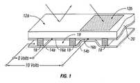
- FIG. 1is an isometric view depicting a portion of one embodiment of an interferometric modulator display in which a movable reflective layer of a first interferometric modulator is in a released position and a movable reflective layer of a second interferometric modulator is in an actuated position.
- FIG. 2is a system block diagram illustrating one embodiment of an electronic device incorporating a 3 ⁇ 3 interferometric modulator display.
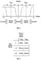
- FIG. 3is a diagram of movable mirror position versus applied voltage for one exemplary embodiment of an interferometric modulator of FIG. 1 .
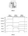
- FIG. 4is an illustration of a set of row and column voltages that may be used to drive an interferometric modulator display.
- FIGS. 5A and 5Billustrate one exemplary timing diagram for row and column signals that may be used to write a frame of display data to the 3 ⁇ 3 interferometric modulator display of FIG. 2 .
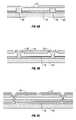
- FIG. 6Ais a cross section of the device of FIG. 1 .
- FIG. 6Bis a cross section of an alternative embodiment of an interferometric modulator.
- FIG. 6Cis a cross section of another alternative embodiment of an interferometric modulator.
- FIG. 7Ais a cross-sectional view of a basic package structure for an interferometric modulator device.
- FIG. 7Bis an isometric view of the package structure of FIG. 7A with a metal seal.
- FIGS. 8A-8Eare cross-sectional views illustrating progressive stages of one embodiment of a method of forming a metal seal and packaging a MEMS device.
- FIG. 9is a flow chart illustrating one embodiment of a method of forming a plated metal seal for a MEMS packaging structure.
- One embodiment of the inventionis a MEMS based device package comprising a MEMS device on a substrate, wherein a seal is positioned proximate a perimeter of the MEMS device and a backplane is joined to the seal so as create a cavity to encapsulate the MEMS device.
- the sealpreferably comprises one or more metal layers insulated from the substrate, wherein the seal is configured to prevent moisture from entering the package.
- the following detailed descriptionis directed to certain specific embodiments of the invention. However, the invention can be embodied in a multitude of different ways. In this description, reference is made to the drawings wherein like parts are designated with like numerals throughout. As will be apparent from the following description, the invention may be implemented in any device that is configured to display an image, whether in motion (e.g., video) or stationary (e.g., still image), and whether textual or pictorial.
- motione.g., video
- stationarye.g., still image
- the inventionmay be implemented in or associated with a variety of electronic devices such as, but not limited to, mobile telephones, wireless devices, personal data assistants (PDAs), hand-held or portable computers, GPS receivers/navigators, cameras, MP3 players, camcorders, game consoles, wrist watches, clocks, calculators, television monitors, flat panel displays, computer monitors, auto displays (e.g., odometer display, etc.), cockpit controls and/or displays, display of camera views (e.g., display of a rear view camera in a vehicle), electronic photographs, electronic billboards or signs, projectors, architectural structures, packaging, and aesthetic structures (e.g., display of images on a piece of jewelry).
- MEMS devices of similar structure to those described hereincan also be used in non-display applications such as in electronic switching devices.
- FIG. 1One interferometric modulator display embodiment comprising an interferometric MEMS display element is illustrated in FIG. 1 .
- the pixelsare in either a bright or dark state.
- the display elementIn the bright (“on” or “open”) state, the display element reflects a large portion of incident visible light to a user.
- the dark (“off” or “closed”) stateWhen in the dark (“off” or “closed”) state, the display element reflects little incident visible light to the user.
- the light reflectance properties of the “on” and “off” statesmay be reversed.
- MEMS pixelscan be configured to reflect predominantly at selected colors, allowing for a color display in addition to black and white.
- FIG. 1is an isometric view depicting two adjacent pixels in a series of pixels of a visual display, wherein each pixel comprises a MEMS interferometric modulator.
- an interferometric modulator displaycomprises a row/column array of these interferometric modulators.
- Each interferometric modulatorincludes a pair of reflective layers positioned at a variable and controllable distance from each other to form a resonant optical cavity with at least one variable dimension.
- one of the reflective layersmay be moved between two positions. In the first position, referred to herein as the released state, the movable layer is positioned at a relatively large distance from a fixed partially reflective layer.
- the movable layerIn the second position, the movable layer is positioned more closely adjacent to the partially reflective layer. Incident light that reflects from the two layers interferes constructively or destructively depending on the position of the movable reflective layer, producing either an overall reflective or non-reflective state for each pixel.
- the depicted portion of the pixel array in FIG. 1includes two adjacent interferometric modulators 12 a and 12 b .
- a movable and highly reflective layer 14 ais illustrated in a released position at a predetermined distance from a fixed partially reflective layer 16 a .
- the movable highly reflective layer 14 bis illustrated in an actuated position adjacent to the fixed partially reflective layer 16 b.
- the fixed layers 16 a , 16 bare electrically conductive, partially transparent and partially reflective, and may be fabricated, for example, by depositing one or more layers each of chromium and indium-tin-oxide onto a transparent substrate 20 .
- the layersare patterned into parallel strips, and may form row electrodes in a display device as described further below.
- the movable layers 14 a , 14 bmay be formed as a series of parallel strips of a deposited metal layer or layers (orthogonal to the row electrodes 16 a , 16 b ) deposited on top of posts 18 and an intervening sacrificial material deposited between the posts 18 .
- the deformable metal layersare separated from the fixed metal layers by a defined air gap 19 .
- a highly conductive and reflective materialsuch as aluminum may be used for the deformable layers, and these strips may form column electrodes in a display device.
- the cavity 19remains between the layers 14 a , 16 a and the deformable layer is in a mechanically relaxed state as illustrated by the pixel 12 a in FIG. 1 .
- the capacitor formed at the intersection of the row and column electrodes at the corresponding pixelbecomes charged, and electrostatic forces pull the electrodes together.
- the movable layeris deformed and is forced against the fixed layer (a dielectric material which is not illustrated in this Figure may be deposited on the fixed layer to prevent shorting and control the separation distance) as illustrated by the pixel 12 b on the right in FIG. 1 .
- the behavioris the same regardless of the polarity of the applied potential difference. In this way, row/column actuation that can control the reflective vs. non-reflective pixel states is analogous in many ways to that used in conventional LCD and other display technologies.
- FIGS. 2 through 5illustrate one exemplary process and system for using an array of interferometric modulators in a display application.
- FIG. 2is a system block diagram illustrating one embodiment of an electronic device that may incorporate aspects of the invention.
- the electronic deviceincludes a processor 21 which may be any general purpose single- or multi-chip microprocessor such as an ARM, Pentium®, Pentium II®, Pentium III®, Pentium IV®, Pentium® Pro, an 8051, a MIPS®, a Power PC®, an ALPHA®, or any special purpose microprocessor such as a digital signal processor, microcontroller, or a programmable gate array.
- the processor 21may be configured to execute one or more software modules.
- the processormay be configured to execute one or more software applications, including a web browser, a telephone application, an email program, or any other software application.
- the processor 21is also configured to communicate with an array controller 22 .
- the array controller 22includes a row driver circuit 24 and a column driver circuit 26 that provide signals to a pixel array 30 .
- the cross section of the array illustrated in FIG. 1is shown by the lines 1 - 1 in FIG. 2 .
- the row/column actuation protocolmay take advantage of a hysteresis property of these devices illustrated in FIG. 3 . It may require, for example, a 10 volt potential difference to cause a movable layer to deform from the released state to the actuated state. However, when the voltage is reduced from that value, the movable layer maintains its state as the voltage drops back below 10 volts.
- the movable layerdoes not release completely until the voltage drops below 2 volts.
- There is thus a range of voltage, about 3 to 7 V in the example illustrated in FIG. 3where there exists a window of applied voltage within which the device is stable in either the released or actuated state. This is referred to herein as the “hysteresis window” or “stability window.”
- hysteresis windowor “stability window.”
- the row/column actuation protocolcan be designed such that during row strobing, pixels in the strobed row that are to be actuated are exposed to a voltage difference of about 10 volts, and pixels that are to be released are exposed to a voltage difference of close to zero volts. After the strobe, the pixels are exposed to a steady state voltage difference of about 5 volts such that they remain in whatever state the row strobe put them in. After being written, each pixel sees a potential difference within the “stability window” of 3-7 volts in this example. This feature makes the pixel design illustrated in FIG. 1 stable under the same applied voltage conditions in either an actuated or released pre-existing state.
- each pixel of the interferometric modulatoris essentially a capacitor formed by the fixed and moving reflective layers, this stable state can be held at a voltage within the hysteresis window with almost no power dissipation. Essentially no current flows into the pixel if the applied potential is fixed.
- a display framemay be created by asserting the set of column electrodes in accordance with the desired set of actuated pixels in the first row.
- a row pulseis then applied to the row 1 electrode, actuating the pixels corresponding to the asserted column lines.
- the asserted set of column electrodesis then changed to correspond to the desired set of actuated pixels in the second row.
- a pulseis then applied to the row 2 electrode, actuating the appropriate pixels in row 2 in accordance with the asserted column electrodes.
- the row 1 pixelsare unaffected by the row 2 pulse, and remain in the state they were set to during the row 1 pulse. This may be repeated for the entire series of rows in a sequential fashion to produce the frame.
- the framesare refreshed and/or updated with new display data by continually repeating this process at some desired number of frames per second.
- protocols for driving row and column electrodes of pixel arrays to produce display framesare also well known and may be used in conjunction with the present invention.
- FIGS. 4 and 5illustrate one possible actuation protocol for creating a display frame on the 3 ⁇ 3 array of FIG. 2 .
- FIG. 4illustrates a possible set of column and row voltage levels that may be used for pixels exhibiting the hysteresis curves of FIG. 3 .
- actuating a pixelinvolves setting the appropriate column to ⁇ V bias , and the appropriate row to + ⁇ V, which may correspond to ⁇ 5 volts and +5 volts respectively Releasing the pixel is accomplished by setting the appropriate column to +V bias , and the appropriate row to the same + ⁇ V, producing a zero volt potential difference across the pixel. In those rows where the row voltage is held at zero volts, the pixels are stable in whatever state they were originally in, regardless of whether the column is at +V bias , or ⁇ V bias .
- FIG. 5Bis a timing diagram showing a series of row and column signals applied to the 3 ⁇ 3 array of FIG. 2 which will result in the display arrangement illustrated in FIG. 5A , where actuated pixels are non-reflective.
- the pixelsPrior to writing the frame illustrated in FIG. 5A , the pixels can be in any state, and in this example, all the rows are at 0 volts, and all the columns are at +5 volts. With these applied voltages, all pixels are stable in their existing actuated or released states.
- pixels ( 1 , 1 ), ( 1 , 2 ), ( 2 , 2 ), ( 3 , 2 ) and ( 3 , 3 )are actuated.
- columns 1 and 2are set to ⁇ 5 volts
- column 3is set to +5 volts. This does not change the state of any pixels, because all the pixels remain in the 3-7 volt stability window.
- Row 1is then strobed with a pulse that goes from 0, up to 5 volts, and back to zero. This actuates the ( 1 , 1 ) and ( 1 , 2 ) pixels and releases the ( 1 , 3 ) pixel. No other pixels in the array are affected.
- row 2is set to ⁇ 5 volts, and columns 1 and 3 are set to +5 volts.
- the same strobe applied to row 2will then actuate pixel ( 2 , 2 ) and release pixels ( 2 , 1 ) and ( 2 , 3 ). Again, no other pixels of the array are affected.
- Row 3is similarly set by setting columns 2 and 3 to ⁇ 5 volts, and column 1 to +5 volts.
- the row 3strobe sets the row 3 pixels as shown in FIG. 5A . After writing the frame, the row potentials are zero, and the column potentials can remain at either +5 or ⁇ 5 volts, and the display is then stable in the arrangement of FIG. 5A .
- FIGS. 6A-6Cillustrate three different embodiments of the moving mirror structure.
- FIG. 6Ais a cross section of the embodiment of FIG. 1 , where a strip of metal material 14 is deposited on orthogonally extending supports 18 .
- the moveable reflective material 14is attached to supports at the corners only, on tethers 32 .
- the moveable reflective material 14is suspended from a deformable layer 34 .
- This embodimenthas benefits because the structural design and materials used for the reflective material 14 can be optimized with respect to the optical properties, and the structural design and materials used for the deformable layer 34 can be optimized with respect to desired mechanical properties.
- FIG. 7AA schematic of a basic package structure for a MEMS device, such as an interferometric modulator array, is illustrated in FIG. 7A .
- a basic package structure 70includes a substrate 72 and a backplane cover or “cap” 74 , wherein an interferometric modulator array 76 is formed on the substrate 72 .
- This cap 74is also called a “backplane”.
- the substrate 72 and the backplane 74are joined by a seal 78 to form the package structure 70 , such that the interferometric modulator array 76 is encapsulated by the substrate 72 , backplane 74 , and the seal 78 .
- the seal 78may be a non-hermetic seal, such as a conventional epoxy-based adhesive.
- the seal 78may be a polyisobutylene (sometimes called butyl rubber, and other times PIB), o-rings, polyurethane, thin film metal weld, liquid spin-on glass, solder, polymers, or plastics, among other types of seals that may have a range of permeability of water vapor of about 0.2-4.7 g mm/m 2 kPa day.
- the seal 78may be a hermetic seal.
- the package structure 70includes a desiccant 80 configured to reduce moisture within the cavity 79 .
- a desiccantmay not be necessary for a hermetically sealed package, but may be desirable to control moisture resident within the package.
- the desiccant 80is positioned between the interferometric modulator array 76 and the backplane 74 .
- Desiccantsmay be used for packages that have either hermetic or non-hermetic seals. In packages having a hermetic seal, desiccants are typically used to control moisture resident within the interior of the package. In packages having a non-hermetic seal, a desiccant may be used to control moisture moving into the package from the environment.
- any substance that can trap moisture while not interfering with the optical properties of the interferometric modulator arraymay be used as the desiccant 80 .
- Suitable desiccant materialsinclude, but are not limited to, zeolites, molecular sieves, surface adsorbents, bulk adsorbents, and chemical reactants.
- the desiccant 80may be in different forms, shapes, and sizes. In addition to being in solid form, the desiccant 80 may alternatively be in powder form. These powders may be inserted directly into the package or they may be mixed with an adhesive for application. In an alternative embodiment, the desiccant 80 may be formed into different shapes, such as cylinders or sheets, before being applied inside the package.
- the desiccant 80can be applied in different ways.
- the desiccant 80is deposited as part of the interferometric modulator array 76 .
- the desiccant 80is applied inside the package 70 as a spray or a dip coat.
- the substrate 72may be a semi-transparent or transparent substance capable of having thin film, MEMS devices built upon it. Such transparent substances include, but are not limited to, glass, plastic, and transparent polymers.
- the interferometric modulator array 76may comprise membrane modulators or modulators of the separable type.
- the backplane 74may be formed of any suitable material, such as glass, metal, foil, polymer, plastic, ceramic, or semiconductor materials (e.g., silicon).
- the packaging processmay be accomplished in a vacuum, pressure between a vacuum up to and including ambient pressure, or pressure higher than ambient pressure.
- the packaging processmay also be accomplished in an environment of varied and controlled high or low pressure during the sealing process.
- the packaging environmentmay be of an inert gas at ambient conditions. Packaging at ambient conditions allows for a lower cost process and more potential for versatility in equipment choice because the device may be transported through ambient conditions without affecting the operation of the device.
- the movable elementmay become permanently stuck to the surface.
- a desiccantmay be used to control moisture resident within the package structure 70 .
- the need for a desiccantcan be reduced or eliminated with the implementation of a hermetic seal 78 to prevent moisture from traveling from the atmosphere into the interior of the package structure 70 .
- the continued reduction in display device dimensionsrestricts available methods to manage the environment within the package structure 70 because there is less area to place a desiccant 80 within the package structure 70 .
- the area of a packaging structure susceptible to influx of water vapormay remain the same or be slightly reduced as package structures are reduced in size, the area available for a desiccant is reduced dramatically in comparison.
- the elimination of the need for a desiccantalso allows the package structure 70 to be thinner, which is desirable in some embodiments.
- the lifetime expectation of the packaged devicemay depend on the lifetime of the desiccant. When the desiccant is fully consumed, the interferometric modulator device may fail as sufficient moisture enters the package structure and damages the interferometric modulator array.
- the seal 78comprises a plated metal that forms a barrier configured to act as an environmental barrier inhibiting or preventing moisture flow therethrough.
- FIG. 7Bis an isometric illustration of a packaging structure 70 with a metal seal 78 .
- the seal 78is a hermetic seal that prevents air and water vapor flow through the seal 78 .
- the metal seal 78is preferably formed according to a photolithographic process and allows for positioning of the seal 78 within +/ ⁇ 1 ⁇ m of a desired position.
- FIGS. 8A-8Eare cross-sectional views illustrating different stages of one embodiment of a method of forming the seal 78 illustrated in FIG. 7B , and packaging a MEMS device such as the interferometric modulator array 76 .
- FIG. 8Ais a cross-sectional view illustrating the interferometric modulator array 76 formed on the substrate 72 .
- the interferometric modulator array 76still comprises a sacrificial layer (not shown) between the conductive members, such as the conductive members 14 , 16 illustrated in FIG. 1 , of the interferometric modulator elements of the array 76 .
- the sacrificial layermay comprise molybdenum, for example.
- conductive leads 801 on the substrate 72are electrically isolated from the seal by depositing an insulator 802 over the substrate 72 .
- the insulator 802is also deposited over the interferometric modulator array 76 , as illustrated in FIG.
- the insulator 802may be applied to a location on the substrate 72 where the seal 78 is to be formed. However, it may be more practical to form the insulator 802 by deposition on top of the substrate 72 and interferometric modulator array 76 as illustrated in FIG. 8B , and subsequently remove undesired portions of the insulator 802 .
- the insulatorcan be formed, for example, by thin film deposition methods such as sputtering or chemical vapor deposition (CVD).
- the insulatoris Si0 2 or other insulating oxide or nitride, and has a thickness of about 2000 ⁇ or less, or about 1000 ⁇ or less. As will be appreciated by those skilled in the technology, other methods of deposition of the insulator and alternative insulator materials are within the scope of the invention.
- the metal layer 804may comprise a plurality of layers, and in one embodiment, the metal layers 804 include an adhesion layer and a metal seed layer.
- the adhesion layerpreferably promotes adhesion between the insulator and the metal seed layer.
- the metal seed layeris a conductive plating base upon which electrodeposit is formed and does not need to be the same material as the electrodeposit.
- the metal seed layerhas a thickness of about 500-2000 ⁇ and the adhesion layer has a thickness of about 50-100 ⁇ .
- the combined thickness of the adhesion layer and the metal seed layeris about 100-500 ⁇ .
- the adhesion layercomprises different types of metal, such as titanium (Ti) or chromium (Cr). The skilled artisan will understand that it is also possible to dispense with the adhesion layer if the surface to which the metal seed layer is to be attached is rough, for example.
- a mask 806is patterned over the metal layers 804 to define one or more cavities 808 for the formation of the sealant wall proximate a perimeter of the interferometric modulator array 76 .
- the perimeter cavity 808may be square or rectangular, or may have other geometries.
- the seal 78is positioned around a total perimeter of the plurality of interferometric modulator arrays.
- the metal layers 804are deposited after patterning the mask 806 , such that the metal layers 804 are deposited on the insulator 802 only in the cavities 808 .
- the mask 806preferably comprises photoresist and can be patterned using UV light, for example.
- the photoresistcan comprise an organic polymer that becomes soluble when exposed to ultraviolet light and prevents etching or plating of the area it covers (this is also known as resist).
- Photoresist and the use thereofis well known in various industries such as semiconductor, biomedical engineering, holographic, electronics, and nanofabrication. In certain embodiments, the use of photoresist as the mask is preferable so as to define thick layers with precision.
- one or more layers of metalare deposited onto the exposed metal seed layer 804 in the cavity 808 , thereby forming a sealant wall 810 .
- Deposition of the one or more metal layerspreferably comprises electroplating using an electroplating bath. Other methods of depositing or forming the metal layers are contemplated, including, for example, electroless plating.
- the thickness of the mask 806is dependent upon the desired thickness or height of the sealant wall 810 , wherein the thickness of the mask 806 is substantially the same or slightly greater than the desired height of the sealant wall 810 .
- the mask 806is thicker than the desired height of the sealant wall 810 , or less thick than the desired height of the sealant wall 810 .
- the height of the sealant wall 810is about 10-70 ⁇ m. In some embodiments, the height of the sealant wall 810 is about 30-50 ⁇ m. Other heights for the sealant wall 810 are contemplated.
- the mask 806 , metal layers 804 , and insulator 802are removed at areas not covered by the electroplated metal 808 by a method such as a wet chemical etch. Alternatively, the metal layers 804 and insulator 802 may each be removed in separate steps. In the embodiment wherein the metal seed layer is deposited on top of the mask 806 , the metal seed layer is removed with the mask 806 . Prior to joining the backplane 74 to the seal 78 , the sacrificial layer present in the interferometric modulator array 76 is etched, using XeF 2 gas for example, to release the membranes or conductive members of the interferometric modulator elements of the array 76 .
- the backplane 74is joined to the seal 78 , which includes the insulator 802 and sealant wall 810 , to form the package structure 70 .
- the backplane 74may be formed of any suitable material, such as glass, metal, foil, polymer, plastic, ceramic, or semiconductor materials (e.g., silicon).
- the seal 78is directly proportional to the height of the sealant wall 810 .
- the seal 78is preferably formed to a height of about 100-300 ⁇ m. In other embodiments, the seal 78 is preferably formed to a height of less than about 400 ⁇ m. In other embodiments, the seal 78 is preferably formed to a thickness greater than about 50 ⁇ m.
- the thickness of the seal 78may depend on various factors, such as the desired lifetime of the interferometric modulator array 76 , the material of the seal 78 , the amount of contaminants and moisture that are estimated to permeate into the package structure 70 during the lifetime of the array 76 , the humidity of the ambient environment, and/or whether a desiccant 80 is included within the package structure 70 .
- FIG. 9is a process flow diagram illustrating one embodiment of a method of forming a metal seal and packaging a MEMS device.
- the structure illustrated in FIG. 8Ais the beginning structure for performance of the method 900 of FIG. 9 , which begins in a step 902 .
- the method 900proceeds to a step 902 wherein the seal is electrically isolated from conductive leads located on the substrate by depositing an insulator over the substrate and the interferometric modulator array, as illustrated in FIG. 8B .
- one or more metal layers for electroplatingare deposited directly on top of the insulator in a step 906 .
- the one or more metal layersmay comprise a plurality of layers, and in one embodiment, the metal layers include an adhesion layer and a metal seed layer.
- a maskis patterned over the metal layers formed in step 906 in order to define one or more cavities 808 for the formation of the sealant wall proximate a perimeter of the interferometric modulator array.
- electroplatingis performed using an electroplating bath to deposit one or more layers of metal onto the exposed metal seed layer in the cavity formed in step 908 , thereby forming a sealant wall.
- Electroplatingis capable of depositing over half of the elements of the periodic table.
- the preferred electroplating metalis nickel, however, copper and tin may also be used.
- Electroplatingis an efficient method of achieving the desired thickness of the seal, which is in the order of tens to hundreds of microns. Methods other than electroplating may be used to deposit metal for the sealant wall including electroless plating, evaporation, and sputtering, for example.
- Step 910may also include electroplating a backplane adhesion layer to the sealant wall, wherein the backplane adhesion layer comprises a solder, such as PbSn, InSb, SnBi, or other solders capable of being plated.
- the backplane adhesion layercomprises multiple layers, such as a wettable metal layer and a solder layer.
- the mask, metal layers, and insulatorare removed at areas not covered by the electroplated metal by a method such as a wet chemical etch.
- the metal layers 804 and insulator 802may each be removed in separate steps.
- the metal seed layermay be removed by ion milling, for example. In the embodiment wherein the metal seed layer is deposited on top of the mask 806 , the metal seed layer is removed with the mask 806 .
- step 914prior to joining the backplane to the sealant wall, the sacrificial layer present in the interferometric modulator array is etched, using XeF 2 gas for example, to release the membranes or conductive members of the interferometric modulator elements of the array. Retaining the sacrificial layer through the seal formation process 900 may be preferable to protect the array from damage that can occur during any steps of the seal forming process 900 . However, the sacrificial molybdenum can be removed any other times during the fabrication process.
- the backplaneis joined to the sealant wall to form the package structure.
- the backplaneis joined to the sealant wall by solder to create a hermetic joint.
- the soldercan be deposited on the sealant wall as discussed in reference to step 910 , can be applied after steps 912 and/or 914 , or can be applied to the backplane.
- the solderpreferably melts and flows at a temperature less than about 250° C. so as to avoid heat damage to the interferometric modulator array 76 .
- the backplanemay have one or more backplane adhesion layers deposited thereon for adhesion to the sealant wall, or wettable metal and/or solder deposited on the sealant wall.
- the backplanecomprises an adhesion layer, such as a thin metal like Cr or Ti, or other material configured to withstand soldering temperatures, and solder is deposited on the adhesion layer for attachment of the backplane to the sealant wall.
- the backplanecomprises a metal that is readily solderable.
- the backplanecomprises a thin film of metal or a path of metal that is soldered to the sealant wall or joined using a seamseal. The formation of the seal 78 reduces the complexity of the packaging process by making the formation of the seal part of the array process.
Landscapes
- Engineering & Computer Science (AREA)
- Physics & Mathematics (AREA)
- Microelectronics & Electronic Packaging (AREA)
- Manufacturing & Machinery (AREA)
- General Physics & Mathematics (AREA)
- Computer Hardware Design (AREA)
- Power Engineering (AREA)
- Condensed Matter Physics & Semiconductors (AREA)
- Spectroscopy & Molecular Physics (AREA)
- Optics & Photonics (AREA)
- Mechanical Light Control Or Optical Switches (AREA)
- Micromachines (AREA)
- Pressure Sensors (AREA)
Abstract
Description
Claims (34)
Priority Applications (1)
| Application Number | Priority Date | Filing Date | Title |
|---|---|---|---|
| US11/779,185US7642127B2 (en) | 2004-09-27 | 2007-07-17 | Method and system for sealing a substrate |
Applications Claiming Priority (3)
| Application Number | Priority Date | Filing Date | Title |
|---|---|---|---|
| US61356904P | 2004-09-27 | 2004-09-27 | |
| US11/089,769US7259449B2 (en) | 2004-09-27 | 2005-03-16 | Method and system for sealing a substrate |
| US11/779,185US7642127B2 (en) | 2004-09-27 | 2007-07-17 | Method and system for sealing a substrate |
Related Parent Applications (1)
| Application Number | Title | Priority Date | Filing Date |
|---|---|---|---|
| US11/089,769DivisionUS7259449B2 (en) | 2004-09-27 | 2005-03-16 | Method and system for sealing a substrate |
Publications (2)
| Publication Number | Publication Date |
|---|---|
| US20070298541A1 US20070298541A1 (en) | 2007-12-27 |
| US7642127B2true US7642127B2 (en) | 2010-01-05 |
Family
ID=35482112
Family Applications (4)
| Application Number | Title | Priority Date | Filing Date |
|---|---|---|---|
| US11/089,769Expired - Fee RelatedUS7259449B2 (en) | 2004-09-27 | 2005-03-16 | Method and system for sealing a substrate |
| US11/779,185Expired - Fee RelatedUS7642127B2 (en) | 2004-09-27 | 2007-07-17 | Method and system for sealing a substrate |
| US11/842,916Expired - Fee RelatedUS7629678B2 (en) | 2004-09-27 | 2007-08-21 | Method and system for sealing a substrate |
| US12/628,024Expired - Fee RelatedUS7935555B2 (en) | 2004-09-27 | 2009-11-30 | Method and system for sealing a substrate |
Family Applications Before (1)
| Application Number | Title | Priority Date | Filing Date |
|---|---|---|---|
| US11/089,769Expired - Fee RelatedUS7259449B2 (en) | 2004-09-27 | 2005-03-16 | Method and system for sealing a substrate |
Family Applications After (2)
| Application Number | Title | Priority Date | Filing Date |
|---|---|---|---|
| US11/842,916Expired - Fee RelatedUS7629678B2 (en) | 2004-09-27 | 2007-08-21 | Method and system for sealing a substrate |
| US12/628,024Expired - Fee RelatedUS7935555B2 (en) | 2004-09-27 | 2009-11-30 | Method and system for sealing a substrate |
Country Status (11)
| Country | Link |
|---|---|
| US (4) | US7259449B2 (en) |
| EP (1) | EP1640325A3 (en) |
| JP (1) | JP4331148B2 (en) |
| KR (1) | KR20060092891A (en) |
| AU (1) | AU2005203429A1 (en) |
| BR (1) | BRPI0503940A (en) |
| CA (1) | CA2516576A1 (en) |
| MX (1) | MXPA05009421A (en) |
| RU (1) | RU2005129864A (en) |
| SG (1) | SG121061A1 (en) |
| TW (1) | TW200627602A (en) |
Cited By (5)
| Publication number | Priority date | Publication date | Assignee | Title |
|---|---|---|---|---|
| US20100072595A1 (en)* | 2004-09-27 | 2010-03-25 | Qualcomm Mems Technologies, Inc. | Method and system for sealing a substrate |
| US20110096508A1 (en)* | 2009-10-23 | 2011-04-28 | Qualcomm Mems Technologies, Inc. | Light-based sealing and device packaging |
| WO2011130715A2 (en) | 2010-04-16 | 2011-10-20 | Flex Lighting Ii, Llc | Illumination device comprising a film-based lightguide |
| WO2011130718A2 (en) | 2010-04-16 | 2011-10-20 | Flex Lighting Ii, Llc | Front illumination device comprising a film-based lightguide |
| US10908408B2 (en)* | 2018-01-03 | 2021-02-02 | Boe Technology Group Co., Ltd. | Pixel structure, method for manufacturing pixel structure array substrate, and display device |
Families Citing this family (22)
| Publication number | Priority date | Publication date | Assignee | Title |
|---|---|---|---|---|
| US7405924B2 (en)* | 2004-09-27 | 2008-07-29 | Idc, Llc | System and method for protecting microelectromechanical systems array using structurally reinforced back-plate |
| EP2495212A3 (en) | 2005-07-22 | 2012-10-31 | QUALCOMM MEMS Technologies, Inc. | Mems devices having support structures and methods of fabricating the same |
| US20070070608A1 (en)* | 2005-09-29 | 2007-03-29 | Skyworks Solutions, Inc. | Packaged electronic devices and process of manufacturing same |
| US7572665B2 (en)* | 2005-10-21 | 2009-08-11 | Wisconsin Alumni Research Foundation | Microelectronics grade metal substrate, related metal-embedded devices and methods for fabricating same |
| US7561334B2 (en)* | 2005-12-20 | 2009-07-14 | Qualcomm Mems Technologies, Inc. | Method and apparatus for reducing back-glass deflection in an interferometric modulator display device |
| US7547568B2 (en)* | 2006-02-22 | 2009-06-16 | Qualcomm Mems Technologies, Inc. | Electrical conditioning of MEMS device and insulating layer thereof |
| WO2007120887A2 (en)* | 2006-04-13 | 2007-10-25 | Qualcomm Mems Technologies, Inc | Packaging a mems device using a frame |
| EP2029473A2 (en)* | 2006-06-21 | 2009-03-04 | Qualcomm Incorporated | Method for packaging an optical mems device |
| DE102007044806A1 (en)* | 2007-09-20 | 2009-04-02 | Robert Bosch Gmbh | Micromechanical component and method for producing a micromechanical component |
| US20100020382A1 (en)* | 2008-07-22 | 2010-01-28 | Qualcomm Mems Technologies, Inc. | Spacer for mems device |
| DE102008042139A1 (en)* | 2008-09-16 | 2010-03-18 | Robert Bosch Gmbh | Exhaust gas protective layers for high temperature ChemFET exhaust gas sensors |
| US8445306B2 (en) | 2008-12-24 | 2013-05-21 | International Business Machines Corporation | Hybrid MEMS RF switch and method of fabricating same |
| US8211728B2 (en)* | 2009-03-27 | 2012-07-03 | International Business Machines Corporation | Horizontal micro-electro-mechanical-system switch |
| US8604898B2 (en) | 2009-04-20 | 2013-12-10 | International Business Machines Corporation | Vertical integrated circuit switches, design structure and methods of fabricating same |
| US8569091B2 (en)* | 2009-08-27 | 2013-10-29 | International Business Machines Corporation | Integrated circuit switches, design structure and methods of fabricating the same |
| US8058106B2 (en)* | 2009-09-04 | 2011-11-15 | Magic Technologies, Inc. | MEMS device package with vacuum cavity by two-step solder reflow method |
| US20130106875A1 (en)* | 2011-11-02 | 2013-05-02 | Qualcomm Mems Technologies, Inc. | Method of improving thin-film encapsulation for an electromechanical systems assembly |
| US20140028686A1 (en)* | 2012-07-27 | 2014-01-30 | Qualcomm Mems Technologies, Inc. | Display system with thin film encapsulated inverted imod |
| US9249014B2 (en)* | 2012-11-06 | 2016-02-02 | Infineon Technologies Austria Ag | Packaged nano-structured component and method of making a packaged nano-structured component |
| RU2561195C2 (en)* | 2012-12-26 | 2015-08-27 | Открытое акционерное общество "Центральный научно-исследовательский институт измерительной аппаратуры" | Membrane-type device |
| WO2020079708A1 (en)* | 2018-10-17 | 2020-04-23 | INDIAN INSTITUTE OF TECHNOLOGY MADRAS (IIT Madras) | A method for fabricating microfluidic devices on porous substrate |
| CN112509992B (en)* | 2020-11-30 | 2024-07-02 | 武汉天马微电子有限公司 | Display panel, electronic device and method for manufacturing display panel |
Citations (113)
| Publication number | Priority date | Publication date | Assignee | Title |
|---|---|---|---|---|
| US3704806A (en) | 1971-01-06 | 1972-12-05 | Le T Im Lensoveta | Dehumidifying composition and a method for preparing the same |
| US3900440A (en) | 1972-11-02 | 1975-08-19 | Kuraray Co | Adhesive composition |
| US4036360A (en) | 1975-11-12 | 1977-07-19 | Graham Magnetics Incorporated | Package having dessicant composition |
| US4074480A (en) | 1976-02-12 | 1978-02-21 | Burton Henry W G | Kit for converting single-glazed window to double-glazed window |
| US4431691A (en) | 1979-01-29 | 1984-02-14 | Tremco, Incorporated | Dimensionally stable sealant and spacer strip and composite structures comprising the same |
| JPS596842B2 (en) | 1974-10-01 | 1984-02-15 | ライオン株式会社 | toothpaste composition |
| US4531126A (en) | 1981-05-18 | 1985-07-23 | Societe D'etude Du Radant | Method and device for analyzing a very high frequency radiation beam of electromagnetic waves |
| US4552806A (en) | 1982-07-16 | 1985-11-12 | Kabushiki Kaisha Toyota Chuo Kenkyusho | Cellular glass coated with a heat insulator |
| US4950344A (en) | 1988-12-05 | 1990-08-21 | Lauren Manufacturing Company | Method of manufacturing multiple-pane sealed glazing units |
| US4954789A (en) | 1989-09-28 | 1990-09-04 | Texas Instruments Incorporated | Spatial light modulator |
| US4977009A (en) | 1987-12-16 | 1990-12-11 | Ford Motor Company | Composite polymer/desiccant coatings for IC encapsulation |
| US5018256A (en) | 1990-06-29 | 1991-05-28 | Texas Instruments Incorporated | Architecture and process for integrating DMD with control circuit substrates |
| US5075796A (en) | 1990-05-31 | 1991-12-24 | Eastman Kodak Company | Optical article for multicolor imaging |
| US5091983A (en) | 1987-06-04 | 1992-02-25 | Walter Lukosz | Optical modulation apparatus and measurement method |
| US5095375A (en) | 1991-03-29 | 1992-03-10 | Hughes Aircraft Company | Holographic combiner edge seal design and composition |
| JPH0485859A (en) | 1990-07-26 | 1992-03-18 | Mitsui Petrochem Ind Ltd | Airtightly sealed package and bonding member |
| US5099353A (en) | 1990-06-29 | 1992-03-24 | Texas Instruments Incorporated | Architecture and process for integrating DMD with control circuit substrates |
| US5172262A (en) | 1985-10-30 | 1992-12-15 | Texas Instruments Incorporated | Spatial light modulator and method |
| US5212582A (en) | 1992-03-04 | 1993-05-18 | Texas Instruments Incorporated | Electrostatically controlled beam steering device and method |
| US5216537A (en) | 1990-06-29 | 1993-06-01 | Texas Instruments Incorporated | Architecture and process for integrating DMD with control circuit substrates |
| US5244707A (en) | 1992-01-10 | 1993-09-14 | Shores A Andrew | Enclosure for electronic devices |
| US5293511A (en) | 1993-03-16 | 1994-03-08 | Texas Instruments Incorporated | Package for a semiconductor device |
| US5304419A (en) | 1990-07-06 | 1994-04-19 | Alpha Fry Ltd | Moisture and particle getter for enclosures |
| US5381253A (en) | 1991-11-14 | 1995-01-10 | Board Of Regents Of University Of Colorado | Chiral smectic liquid crystal optical modulators having variable retardation |
| US5547823A (en) | 1993-06-28 | 1996-08-20 | Ishihara Sangyo Kaisha, Ltd. | Photocatalyst composite and process for producing the same |
| US5550373A (en) | 1994-12-30 | 1996-08-27 | Honeywell Inc. | Fabry-Perot micro filter-detector |
| US5553440A (en) | 1994-10-20 | 1996-09-10 | Ppg Industries, Inc. | Multi-sheet glazing unit and method of making same |
| US5559358A (en) | 1993-05-25 | 1996-09-24 | Honeywell Inc. | Opto-electro-mechanical device or filter, process for making, and sensors made therefrom |
| US5646729A (en) | 1993-01-13 | 1997-07-08 | Vaisala Oy | Single-channel gas concentration measurement method and apparatus using a short-resonator Fabry-Perot interferometer |
| US5703710A (en) | 1994-09-09 | 1997-12-30 | Deacon Research | Method for manipulating optical energy using poled structure |
| US5739945A (en) | 1995-09-29 | 1998-04-14 | Tayebati; Parviz | Electrically tunable optical filter utilizing a deformable multi-layer mirror |
| US5815141A (en) | 1996-04-12 | 1998-09-29 | Elo Touch Systems, Inc. | Resistive touchscreen having multiple selectable regions for pressure discrimination |
| US5835255A (en) | 1986-04-23 | 1998-11-10 | Etalon, Inc. | Visible spectrum modulator arrays |
| US5853662A (en) | 1996-04-17 | 1998-12-29 | Mitsubishi Gas Chemical Company, Inc. | Method for preserving polished inorganic glass and method for preserving article obtained by using the same |
| JPH11145337A (en) | 1997-11-12 | 1999-05-28 | Tomoegawa Paper Co Ltd | Electronic component sealing package |
| US5939785A (en) | 1996-04-12 | 1999-08-17 | Texas Instruments Incorporated | Micromechanical device including time-release passivant |
| US6040937A (en) | 1994-05-05 | 2000-03-21 | Etalon, Inc. | Interferometric modulation |
| EP1093162A1 (en) | 1999-10-15 | 2001-04-18 | Lucent Technologies Inc. | Hermatic firewall for mems packaging in flip-chip bonded geometry |
| US6238755B1 (en) | 1997-11-15 | 2001-05-29 | Dow Corning Corporation | Insulating glass units |
| WO2001045140A3 (en) | 1999-12-17 | 2002-01-03 | Osram Opto Semiconductors Gmbh | Encapsulation for organic led device |
| US20020000649A1 (en) | 1998-04-17 | 2002-01-03 | Tilmans Hendrikus A.C. | Method of fabrication of a microstructure having an internal cavity |
| US6355328B1 (en) | 1996-02-27 | 2002-03-12 | Truseal Technologies, Inc. | Preformed flexible laminate |
| US20020056900A1 (en) | 2000-11-16 | 2002-05-16 | Liu Jwei Wien | Electro-optical package with drop-in aperture |
| WO2002042716A2 (en) | 2000-11-27 | 2002-05-30 | Microsensors Inc. | Wafer eutectic bonding of mems gyros |
| US20020075551A1 (en) | 2000-11-29 | 2002-06-20 | Onix Microsystems, Inc | Enclosure for MEMS apparatus and method of using the same |
| US20020075555A1 (en) | 1994-05-05 | 2002-06-20 | Iridigm Display Corporation | Interferometric modulation of radiation |
| US20020121909A1 (en) | 2001-01-23 | 2002-09-05 | Norio Sato | Surface shape recognition sensor and method of manufacturing the same |
| US6455927B1 (en) | 2001-03-12 | 2002-09-24 | Amkor Technology, Inc. | Micromirror device package |
| US6467139B1 (en) | 1998-08-03 | 2002-10-22 | Nec Corporation | Mounting structure and mounting method for surface acoustic wave element |
| US20020160583A1 (en) | 2001-04-26 | 2002-10-31 | Samsung Electronics Co., Ltd. | MEMS relay and mehtod of fabricating the same |
| US6489670B1 (en) | 2000-05-16 | 2002-12-03 | Sandia Corporation | Sealed symmetric multilayered microelectronic device package with integral windows |
| US20020187254A1 (en) | 2001-05-08 | 2002-12-12 | Eastman Kodak Company | Ultrasonically sealing the cover plate to provide a hermetic enclosure for OLED displays |
| WO2003007049A1 (en) | 1999-10-05 | 2003-01-23 | Iridigm Display Corporation | Photonic mems and structures |
| US20030054588A1 (en) | 2000-12-07 | 2003-03-20 | Reflectivity, Inc., A California Corporation | Methods for depositing, releasing and packaging micro-electromechanical devices on wafer substrates |
| US20030053233A1 (en) | 2001-09-20 | 2003-03-20 | Felton Lawrence E. | Optical switching apparatus and method for assembling same |
| WO2003026369A1 (en) | 2001-09-17 | 2003-03-27 | John Stafford | Latching micro magnetic relay packages and methods of packaging |
| US20030062186A1 (en) | 2001-09-21 | 2003-04-03 | Eastman Kodak Company | Sealing structure for highly moisture-sensitive electronic device element and method for fabrication |
| WO2003009318A8 (en) | 2001-07-20 | 2003-04-10 | Getters Spa | Support with getter-material for microelectronic, microoptoelectronic or micromechanical device |
| US20030075794A1 (en) | 2001-10-23 | 2003-04-24 | Felton Lawrence E. | MEMS capping method and apparatus |
| US20030103185A1 (en) | 2001-11-30 | 2003-06-05 | Lg. Philips Lcd Co., Ltd. | Liquid crystal display panel and method for fabricating the same |
| US20030104651A1 (en) | 2001-12-04 | 2003-06-05 | Samsung Electronics Co., Ltd. | Low temperature hermetic sealing method having passivation layer |
| US20030108306A1 (en) | 2001-12-12 | 2003-06-12 | Axsun Technologies, Inc. | MEMS tunable optical filter system with moisture getter for frequency stability |
| US6582789B1 (en) | 1999-10-01 | 2003-06-24 | Teijin Limited | Surface protective film and laminate formed therefrom |
| US6589625B1 (en) | 2001-08-01 | 2003-07-08 | Iridigm Display Corporation | Hermetic seal and method to create the same |
| US6603182B1 (en) | 2002-03-12 | 2003-08-05 | Lucent Technologies Inc. | Packaging micromechanical devices |
| US20030155643A1 (en) | 2002-02-19 | 2003-08-21 | Freidhoff Carl B. | Thin film encapsulation of MEMS devices |
| US6621134B1 (en) | 2002-02-07 | 2003-09-16 | Shayne Zurn | Vacuum sealed RF/microwave microresonator |
| US20030184412A1 (en) | 2002-03-27 | 2003-10-02 | Gorrell Jonathan F. | Tunable MEMS resonator and method for tuning |
| US20030183916A1 (en) | 2002-03-27 | 2003-10-02 | John Heck | Packaging microelectromechanical systems |
| US6650455B2 (en) | 1994-05-05 | 2003-11-18 | Iridigm Display Corporation | Photonic mems and structures |
| US20030214007A1 (en) | 2002-05-17 | 2003-11-20 | Advanced Semiconductor Engineering, Inc. | Wafer-level package with bump and method for manufacturing the same |
| US6661084B1 (en) | 2000-05-16 | 2003-12-09 | Sandia Corporation | Single level microelectronic device package with an integral window |
| WO2003105198A1 (en) | 2002-06-11 | 2003-12-18 | Reflectivity, Inc. | Methods for depositing, releasing and packaging micro-electromechanical devices on wafer substrates |
| FR2841380A1 (en) | 2002-06-25 | 2003-12-26 | Commissariat Energie Atomique | METHOD FOR ENCAPSULATING AN OBJECT UNDER CONTROLLED ATMOSPHERE |
| US6674562B1 (en) | 1994-05-05 | 2004-01-06 | Iridigm Display Corporation | Interferometric modulation of radiation |
| US20040048027A1 (en) | 2002-09-06 | 2004-03-11 | Hayes Michael W. | Honeycomb cores for aerospace applications |
| US6709750B1 (en) | 1998-04-06 | 2004-03-23 | Metallgesellschaft Aktiengesellschaft | Hot-melt adhesive for sealing the edge of laminated glass |
| US20040061492A1 (en) | 2000-11-16 | 2004-04-01 | Lopes Vincent C. | Package with environmental control material carrier |
| US20040066258A1 (en) | 2000-11-29 | 2004-04-08 | Cohn Michael B. | MEMS device with integral packaging |
| US20040070706A1 (en) | 2002-10-10 | 2004-04-15 | Freeman Gary A. | Parallax compensating color filter and black mask for display apparatus |
| EP1418154A2 (en) | 2002-11-08 | 2004-05-12 | Samsung Electronics Co., Ltd. | Method and apparatus for vacuum-mounting a micro electro mechanical system on a substrate |
| US20040100677A1 (en) | 2000-12-07 | 2004-05-27 | Reflectivity, Inc., A California Corporation | Spatial light modulators with light blocking/absorbing areas |
| US6743656B2 (en) | 1999-10-04 | 2004-06-01 | Texas Instruments Incorporated | MEMS wafer level package |
| US20040140557A1 (en) | 2003-01-21 | 2004-07-22 | United Test & Assembly Center Limited | Wl-bga for MEMS/MOEMS devices |
| US6791660B1 (en) | 2002-02-12 | 2004-09-14 | Seiko Epson Corporation | Method for manufacturing electrooptical device and apparatus for manufacturing the same, electrooptical device and electronic appliances |
| US20040184133A1 (en) | 2003-03-18 | 2004-09-23 | Tao Su | Microsystem package structure |
| WO2004025727A8 (en) | 2002-09-10 | 2004-12-23 | Frank Niklaus | Method for sealing a microcavity and package comprising at least one microcavity |
| US6838309B1 (en) | 2002-03-13 | 2005-01-04 | Amkor Technology, Inc. | Flip-chip micromachine package using seal layer |
| US20050023976A1 (en) | 2003-07-07 | 2005-02-03 | Yuxin Wang | Seal and sealing process for electroluminescent displays |
| US20050035699A1 (en) | 2003-08-15 | 2005-02-17 | Hsiung-Kuang Tsai | Optical interference display panel |
| US20050036192A1 (en) | 2003-08-15 | 2005-02-17 | Wen-Jian Lin | Optical interference display panel |
| US20050042117A1 (en) | 2003-08-18 | 2005-02-24 | Wen-Jian Lin | Optical interference display panel and manufacturing method thereof |
| US20050046922A1 (en) | 2003-09-03 | 2005-03-03 | Wen-Jian Lin | Interferometric modulation pixels and manufacturing method thereof |
| US20050046919A1 (en) | 2003-08-29 | 2005-03-03 | Sharp Kabushiki Kaisha | Interferometric modulator and display unit |
| US6872984B1 (en) | 1998-07-29 | 2005-03-29 | Silicon Light Machines Corporation | Method of sealing a hermetic lid to a semiconductor die at an angle |
| US20050093134A1 (en) | 2003-10-30 | 2005-05-05 | Terry Tarn | Device packages with low stress assembly process |
| US20050254115A1 (en)* | 2004-05-12 | 2005-11-17 | Iridigm Display Corporation | Packaging for an interferometric modulator |
| US20050253283A1 (en) | 2004-05-13 | 2005-11-17 | Dcamp Jon B | Getter deposition for vacuum packaging |
| WO2005110914A1 (en) | 2004-05-04 | 2005-11-24 | Idc, Llc | Modifying the electro-mechanical behavior of micromachined devices |
| US7012726B1 (en) | 2003-11-03 | 2006-03-14 | Idc, Llc | MEMS devices with unreleased thin film components |
| US7015885B2 (en) | 2003-03-22 | 2006-03-21 | Active Optical Networks, Inc. | MEMS devices monolithically integrated with drive and control circuitry |
| US20060066935A1 (en) | 2004-09-27 | 2006-03-30 | Cummings William J | Process for modifying offset voltage characteristics of an interferometric modulator |
| US7034984B2 (en) | 2002-06-19 | 2006-04-25 | Miradia Inc. | Fabrication of a high fill ratio reflective spatial light modulator with hidden hinge |
| US20060152106A1 (en) | 2002-11-04 | 2006-07-13 | Jun Yan | Mems scanner with dual magnetic and capacitive drive |
| US20060197215A1 (en) | 2005-03-03 | 2006-09-07 | Stellar Microdevices, Inc. | Hermetic MEMS package and method of manufacture |
| US7119945B2 (en) | 2004-03-03 | 2006-10-10 | Idc, Llc | Altering temporal response of microelectromechanical elements |
| US7126741B2 (en) | 2004-08-12 | 2006-10-24 | Hewlett-Packard Development Company, L.P. | Light modulator assembly |
| US7130104B2 (en) | 2004-09-27 | 2006-10-31 | Idc, Llc | Methods and devices for inhibiting tilting of a mirror in an interferometric modulator |
| US7136213B2 (en) | 2004-09-27 | 2006-11-14 | Idc, Llc | Interferometric modulators having charge persistence |
| US7138984B1 (en) | 2001-06-05 | 2006-11-21 | Idc, Llc | Directly laminated touch sensitive screen |
| US7142346B2 (en) | 2003-12-09 | 2006-11-28 | Idc, Llc | System and method for addressing a MEMS display |
| US20070097477A1 (en) | 1995-05-01 | 2007-05-03 | Miles Mark W | Visible spectrum modulator arrays |
| US7259449B2 (en) | 2004-09-27 | 2007-08-21 | Idc, Llc | Method and system for sealing a substrate |
Family Cites Families (205)
| Publication number | Priority date | Publication date | Assignee | Title |
|---|---|---|---|---|
| US2002A (en)* | 1841-03-12 | Tor and planter for plowing | ||
| US2534846A (en) | 1946-06-20 | 1950-12-19 | Emi Ltd | Color filter |
| DE1288651B (en) | 1963-06-28 | 1969-02-06 | Siemens Ag | Arrangement of electrical dipoles for wavelengths below 1 mm and method for producing such an arrangement |
| FR1603131A (en) | 1968-07-05 | 1971-03-22 | ||
| US3813265A (en) | 1970-02-16 | 1974-05-28 | A Marks | Electro-optical dipolar material |
| US3653741A (en) | 1970-02-16 | 1972-04-04 | Alvin M Marks | Electro-optical dipolar material |
| DE2336930A1 (en) | 1973-07-20 | 1975-02-06 | Battelle Institut E V | INFRARED MODULATOR (II.) |
| US4099854A (en) | 1976-10-12 | 1978-07-11 | The Unites States Of America As Represented By The Secretary Of The Navy | Optical notch filter utilizing electric dipole resonance absorption |
| US4389096A (en) | 1977-12-27 | 1983-06-21 | Matsushita Electric Industrial Co., Ltd. | Image display apparatus of liquid crystal valve projection type |
| US4663083A (en) | 1978-05-26 | 1987-05-05 | Marks Alvin M | Electro-optical dipole suspension with reflective-absorptive-transmissive characteristics |
| US4445050A (en) | 1981-12-15 | 1984-04-24 | Marks Alvin M | Device for conversion of light power to electric power |
| US4228437A (en) | 1979-06-26 | 1980-10-14 | The United States Of America As Represented By The Secretary Of The Navy | Wideband polarization-transforming electromagnetic mirror |
| NL8001281A (en) | 1980-03-04 | 1981-10-01 | Philips Nv | DISPLAY DEVICE. |
| US4377324A (en) | 1980-08-04 | 1983-03-22 | Honeywell Inc. | Graded index Fabry-Perot optical filter device |
| US4441791A (en) | 1980-09-02 | 1984-04-10 | Texas Instruments Incorporated | Deformable mirror light modulator |
| NL8103377A (en) | 1981-07-16 | 1983-02-16 | Philips Nv | DISPLAY DEVICE. |
| US4571603A (en) | 1981-11-03 | 1986-02-18 | Texas Instruments Incorporated | Deformable mirror electrostatic printer |
| NL8200354A (en) | 1982-02-01 | 1983-09-01 | Philips Nv | PASSIVE DISPLAY. |
| US4500171A (en) | 1982-06-02 | 1985-02-19 | Texas Instruments Incorporated | Process for plastic LCD fill hole sealing |
| US4482213A (en) | 1982-11-23 | 1984-11-13 | Texas Instruments Incorporated | Perimeter seal reinforcement holes for plastic LCDs |
| US4566935A (en) | 1984-07-31 | 1986-01-28 | Texas Instruments Incorporated | Spatial light modulator and method |
| US4710732A (en) | 1984-07-31 | 1987-12-01 | Texas Instruments Incorporated | Spatial light modulator and method |
| US4662746A (en) | 1985-10-30 | 1987-05-05 | Texas Instruments Incorporated | Spatial light modulator and method |
| US4596992A (en) | 1984-08-31 | 1986-06-24 | Texas Instruments Incorporated | Linear spatial light modulator and printer |
| US5096279A (en) | 1984-08-31 | 1992-03-17 | Texas Instruments Incorporated | Spatial light modulator and method |
| US5061049A (en) | 1984-08-31 | 1991-10-29 | Texas Instruments Incorporated | Spatial light modulator and method |
| US4615595A (en) | 1984-10-10 | 1986-10-07 | Texas Instruments Incorporated | Frame addressed spatial light modulator |
| GB8610129D0 (en) | 1986-04-25 | 1986-05-29 | Secr Defence | Electro-optical device |
| US4748366A (en) | 1986-09-02 | 1988-05-31 | Taylor George W | Novel uses of piezoelectric materials for creating optical effects |
| US4786128A (en) | 1986-12-02 | 1988-11-22 | Quantum Diagnostics, Ltd. | Device for modulating and reflecting electromagnetic radiation employing electro-optic layer having a variable index of refraction |
| US4956619A (en) | 1988-02-19 | 1990-09-11 | Texas Instruments Incorporated | Spatial light modulator |
| US4856863A (en) | 1988-06-22 | 1989-08-15 | Texas Instruments Incorporated | Optical fiber interconnection network including spatial light modulator |
| US5028939A (en) | 1988-08-23 | 1991-07-02 | Texas Instruments Incorporated | Spatial light modulator system |
| US4982184A (en) | 1989-01-03 | 1991-01-01 | General Electric Company | Electrocrystallochromic display and element |
| US5079544A (en) | 1989-02-27 | 1992-01-07 | Texas Instruments Incorporated | Standard independent digitized video system |
| US5214419A (en) | 1989-02-27 | 1993-05-25 | Texas Instruments Incorporated | Planarized true three dimensional display |
| US5170156A (en) | 1989-02-27 | 1992-12-08 | Texas Instruments Incorporated | Multi-frequency two dimensional display system |
| US5214420A (en) | 1989-02-27 | 1993-05-25 | Texas Instruments Incorporated | Spatial light modulator projection system with random polarity light |
| US5272473A (en) | 1989-02-27 | 1993-12-21 | Texas Instruments Incorporated | Reduced-speckle display system |
| US5162787A (en) | 1989-02-27 | 1992-11-10 | Texas Instruments Incorporated | Apparatus and method for digitized video system utilizing a moving display surface |
| US5287096A (en) | 1989-02-27 | 1994-02-15 | Texas Instruments Incorporated | Variable luminosity display system |
| US5206629A (en) | 1989-02-27 | 1993-04-27 | Texas Instruments Incorporated | Spatial light modulator and memory for digitized video display |
| US5446479A (en) | 1989-02-27 | 1995-08-29 | Texas Instruments Incorporated | Multi-dimensional array video processor system |
| US5192946A (en) | 1989-02-27 | 1993-03-09 | Texas Instruments Incorporated | Digitized color video display system |
| KR100202246B1 (en) | 1989-02-27 | 1999-06-15 | 윌리엄 비. 켐플러 | Apparatus and method for digitalized video system |
| US5022745A (en) | 1989-09-07 | 1991-06-11 | Massachusetts Institute Of Technology | Electrostatically deformable single crystal dielectrically coated mirror |
| US5124834A (en) | 1989-11-16 | 1992-06-23 | General Electric Company | Transferrable, self-supporting pellicle for elastomer light valve displays and method for making the same |
| US5037173A (en) | 1989-11-22 | 1991-08-06 | Texas Instruments Incorporated | Optical interconnection network |
| US5500635A (en) | 1990-02-20 | 1996-03-19 | Mott; Jonathan C. | Products incorporating piezoelectric material |
| CH682523A5 (en) | 1990-04-20 | 1993-09-30 | Suisse Electronique Microtech | A modulation matrix addressed light. |
| US5142405A (en) | 1990-06-29 | 1992-08-25 | Texas Instruments Incorporated | Bistable dmd addressing circuit and method |
| EP0467048B1 (en) | 1990-06-29 | 1995-09-20 | Texas Instruments Incorporated | Field-updated deformable mirror device |
| US5083857A (en) | 1990-06-29 | 1992-01-28 | Texas Instruments Incorporated | Multi-level deformable mirror device |
| US5153771A (en) | 1990-07-18 | 1992-10-06 | Northrop Corporation | Coherent light modulation and detector |
| US5526688A (en) | 1990-10-12 | 1996-06-18 | Texas Instruments Incorporated | Digital flexure beam accelerometer and method |
| US5192395A (en) | 1990-10-12 | 1993-03-09 | Texas Instruments Incorporated | Method of making a digital flexure beam accelerometer |
| US5044736A (en) | 1990-11-06 | 1991-09-03 | Motorola, Inc. | Configurable optical filter or display |
| US5602671A (en) | 1990-11-13 | 1997-02-11 | Texas Instruments Incorporated | Low surface energy passivation layer for micromechanical devices |
| US5331454A (en) | 1990-11-13 | 1994-07-19 | Texas Instruments Incorporated | Low reset voltage process for DMD |
| US5233459A (en) | 1991-03-06 | 1993-08-03 | Massachusetts Institute Of Technology | Electric display device |
| CA2063744C (en) | 1991-04-01 | 2002-10-08 | Paul M. Urbanus | Digital micromirror device architecture and timing for use in a pulse-width modulated display system |
| US5142414A (en) | 1991-04-22 | 1992-08-25 | Koehler Dale R | Electrically actuatable temporal tristimulus-color device |
| US5226099A (en) | 1991-04-26 | 1993-07-06 | Texas Instruments Incorporated | Digital micromirror shutter device |
| US5179274A (en) | 1991-07-12 | 1993-01-12 | Texas Instruments Incorporated | Method for controlling operation of optical systems and devices |
| US5168406A (en) | 1991-07-31 | 1992-12-01 | Texas Instruments Incorporated | Color deformable mirror device and method for manufacture |
| US5254980A (en) | 1991-09-06 | 1993-10-19 | Texas Instruments Incorporated | DMD display system controller |
| US5563398A (en) | 1991-10-31 | 1996-10-08 | Texas Instruments Incorporated | Spatial light modulator scanning system |
| CA2081753C (en) | 1991-11-22 | 2002-08-06 | Jeffrey B. Sampsell | Dmd scanner |
| US5233385A (en) | 1991-12-18 | 1993-08-03 | Texas Instruments Incorporated | White light enhanced color field sequential projection |
| US5233456A (en) | 1991-12-20 | 1993-08-03 | Texas Instruments Incorporated | Resonant mirror and method of manufacture |
| CA2087625C (en) | 1992-01-23 | 2006-12-12 | William E. Nelson | Non-systolic time delay and integration printing |
| US5296950A (en) | 1992-01-31 | 1994-03-22 | Texas Instruments Incorporated | Optical signal free-space conversion board |
| US5231532A (en) | 1992-02-05 | 1993-07-27 | Texas Instruments Incorporated | Switchable resonant filter for optical radiation |
| DE69310974T2 (en) | 1992-03-25 | 1997-11-06 | Texas Instruments Inc | Built-in optical calibration system |
| US5312513A (en) | 1992-04-03 | 1994-05-17 | Texas Instruments Incorporated | Methods of forming multiple phase light modulators |
| WO1993021663A1 (en) | 1992-04-08 | 1993-10-28 | Georgia Tech Research Corporation | Process for lift-off of thin film materials from a growth substrate |
| US5311360A (en) | 1992-04-28 | 1994-05-10 | The Board Of Trustees Of The Leland Stanford, Junior University | Method and apparatus for modulating a light beam |
| JPH0651250A (en) | 1992-05-20 | 1994-02-25 | Texas Instr Inc <Ti> | Monolithic space optical modulator and memory package |
| JPH06214169A (en) | 1992-06-08 | 1994-08-05 | Texas Instr Inc <Ti> | Controllable optical and periodic surface filter |
| US5818095A (en) | 1992-08-11 | 1998-10-06 | Texas Instruments Incorporated | High-yield spatial light modulator with light blocking layer |
| US5327286A (en) | 1992-08-31 | 1994-07-05 | Texas Instruments Incorporated | Real time optical correlation system |
| US5325116A (en) | 1992-09-18 | 1994-06-28 | Texas Instruments Incorporated | Device for writing to and reading from optical storage media |
| US5659374A (en) | 1992-10-23 | 1997-08-19 | Texas Instruments Incorporated | Method of repairing defective pixels |
| EP0610665B1 (en) | 1993-01-11 | 1997-09-10 | Texas Instruments Incorporated | Pixel control circuitry for spatial light modulator |
| US5461411A (en) | 1993-03-29 | 1995-10-24 | Texas Instruments Incorporated | Process and architecture for digital micromirror printer |
| US5489952A (en) | 1993-07-14 | 1996-02-06 | Texas Instruments Incorporated | Method and device for multi-format television |
| US5365283A (en) | 1993-07-19 | 1994-11-15 | Texas Instruments Incorporated | Color phase control for projection display using spatial light modulator |
| US5526172A (en) | 1993-07-27 | 1996-06-11 | Texas Instruments Incorporated | Microminiature, monolithic, variable electrical signal processor and apparatus including same |
| US5581272A (en) | 1993-08-25 | 1996-12-03 | Texas Instruments Incorporated | Signal generator for controlling a spatial light modulator |
| FR2710161B1 (en) | 1993-09-13 | 1995-11-24 | Suisse Electronique Microtech | Miniature array of light shutters. |
| US5457493A (en) | 1993-09-15 | 1995-10-10 | Texas Instruments Incorporated | Digital micro-mirror based image simulation system |
| US5526051A (en) | 1993-10-27 | 1996-06-11 | Texas Instruments Incorporated | Digital television system |
| US5497197A (en) | 1993-11-04 | 1996-03-05 | Texas Instruments Incorporated | System and method for packaging data into video processor |
| US5459602A (en) | 1993-10-29 | 1995-10-17 | Texas Instruments | Micro-mechanical optical shutter |
| US5452024A (en) | 1993-11-01 | 1995-09-19 | Texas Instruments Incorporated | DMD display system |
| US5517347A (en) | 1993-12-01 | 1996-05-14 | Texas Instruments Incorporated | Direct view deformable mirror device |
| CA2137059C (en) | 1993-12-03 | 2004-11-23 | Texas Instruments Incorporated | Dmd architecture to improve horizontal resolution |
| US5583688A (en) | 1993-12-21 | 1996-12-10 | Texas Instruments Incorporated | Multi-level digital micromirror device |
| US5448314A (en) | 1994-01-07 | 1995-09-05 | Texas Instruments | Method and apparatus for sequential color imaging |
| US5500761A (en) | 1994-01-27 | 1996-03-19 | At&T Corp. | Micromechanical modulator |
| US5444566A (en) | 1994-03-07 | 1995-08-22 | Texas Instruments Incorporated | Optimized electronic operation of digital micromirror devices |
| US5665997A (en) | 1994-03-31 | 1997-09-09 | Texas Instruments Incorporated | Grated landing area to eliminate sticking of micro-mechanical devices |
| US6710908B2 (en) | 1994-05-05 | 2004-03-23 | Iridigm Display Corporation | Controlling micro-electro-mechanical cavities |
| US7550794B2 (en) | 2002-09-20 | 2009-06-23 | Idc, Llc | Micromechanical systems device comprising a displaceable electrode and a charge-trapping layer |
| US7460291B2 (en) | 1994-05-05 | 2008-12-02 | Idc, Llc | Separable modulator |
| KR950033432A (en) | 1994-05-12 | 1995-12-26 | 윌리엄 이. 힐러 | Spatial Light Modulator Display Pointing Device |
| US5497172A (en) | 1994-06-13 | 1996-03-05 | Texas Instruments Incorporated | Pulse width modulation for spatial light modulator with split reset addressing |
| US5673106A (en) | 1994-06-17 | 1997-09-30 | Texas Instruments Incorporated | Printing system with self-monitoring and adjustment |
| US5454906A (en) | 1994-06-21 | 1995-10-03 | Texas Instruments Inc. | Method of providing sacrificial spacer for micro-mechanical devices |
| US5499062A (en) | 1994-06-23 | 1996-03-12 | Texas Instruments Incorporated | Multiplexed memory timing with block reset and secondary memory |
| US5636052A (en) | 1994-07-29 | 1997-06-03 | Lucent Technologies Inc. | Direct view display based on a micromechanical modulation |
| US5485304A (en) | 1994-07-29 | 1996-01-16 | Texas Instruments, Inc. | Support posts for micro-mechanical devices |
| US6053617A (en) | 1994-09-23 | 2000-04-25 | Texas Instruments Incorporated | Manufacture method for micromechanical devices |
| US5619059A (en) | 1994-09-28 | 1997-04-08 | National Research Council Of Canada | Color deformable mirror device having optical thin film interference color coatings |
| US5650881A (en) | 1994-11-02 | 1997-07-22 | Texas Instruments Incorporated | Support post architecture for micromechanical devices |
| US5552924A (en) | 1994-11-14 | 1996-09-03 | Texas Instruments Incorporated | Micromechanical device having an improved beam |
| US5610624A (en) | 1994-11-30 | 1997-03-11 | Texas Instruments Incorporated | Spatial light modulator with reduced possibility of an on state defect |
| US5567334A (en) | 1995-02-27 | 1996-10-22 | Texas Instruments Incorporated | Method for creating a digital micromirror device using an aluminum hard mask |
| US5610438A (en) | 1995-03-08 | 1997-03-11 | Texas Instruments Incorporated | Micro-mechanical device with non-evaporable getter |
| US5535047A (en) | 1995-04-18 | 1996-07-09 | Texas Instruments Incorporated | Active yoke hidden hinge digital micromirror device |
| US5784190A (en) | 1995-04-27 | 1998-07-21 | John M. Baker | Electro-micro-mechanical shutters on transparent substrates |
| JP4431196B2 (en) | 1995-11-06 | 2010-03-10 | アイディーシー エルエルシー | Interferometric modulation |
| US5825528A (en) | 1995-12-26 | 1998-10-20 | Lucent Technologies Inc. | Phase-mismatched fabry-perot cavity micromechanical modulator |
| JP3799092B2 (en) | 1995-12-29 | 2006-07-19 | アジレント・テクノロジーズ・インク | Light modulation device and display device |
| US5710656A (en) | 1996-07-30 | 1998-01-20 | Lucent Technologies Inc. | Micromechanical optical modulator having a reduced-mass composite membrane |
| US5912758A (en) | 1996-09-11 | 1999-06-15 | Texas Instruments Incorporated | Bipolar reset for spatial light modulators |
| US5771116A (en) | 1996-10-21 | 1998-06-23 | Texas Instruments Incorporated | Multiple bias level reset waveform for enhanced DMD control |
| US7471444B2 (en) | 1996-12-19 | 2008-12-30 | Idc, Llc | Interferometric modulation of radiation |
| US6092824A (en)* | 1998-02-20 | 2000-07-25 | 210 Innovations Llc | Wheelchair automatic anti-rollback assembly |
| DE69806846T2 (en) | 1997-05-08 | 2002-12-12 | Texas Instruments Inc., Dallas | Improvements for spatial light modulators |
| US6480177B2 (en) | 1997-06-04 | 2002-11-12 | Texas Instruments Incorporated | Blocked stepped address voltage for micromechanical devices |
| US6028690A (en) | 1997-11-26 | 2000-02-22 | Texas Instruments Incorporated | Reduced micromirror mirror gaps for improved contrast ratio |
| US6180428B1 (en) | 1997-12-12 | 2001-01-30 | Xerox Corporation | Monolithic scanning light emitting devices using micromachining |
| WO1999052006A2 (en) | 1998-04-08 | 1999-10-14 | Etalon, Inc. | Interferometric modulation of radiation |
| US6160833A (en) | 1998-05-06 | 2000-12-12 | Xerox Corporation | Blue vertical cavity surface emitting laser |
| US6282010B1 (en) | 1998-05-14 | 2001-08-28 | Texas Instruments Incorporated | Anti-reflective coatings for spatial light modulators |
| US6323982B1 (en) | 1998-05-22 | 2001-11-27 | Texas Instruments Incorporated | Yield superstructure for digital micromirror device |
| US6147790A (en) | 1998-06-02 | 2000-11-14 | Texas Instruments Incorporated | Spring-ring micromechanical device |
| US6295154B1 (en) | 1998-06-05 | 2001-09-25 | Texas Instruments Incorporated | Optical switching apparatus |
| US6496122B2 (en) | 1998-06-26 | 2002-12-17 | Sharp Laboratories Of America, Inc. | Image display and remote control system capable of displaying two distinct images |
| US6113239A (en) | 1998-09-04 | 2000-09-05 | Sharp Laboratories Of America, Inc. | Projection display system for reflective light valves |
| US6606175B1 (en) | 1999-03-16 | 2003-08-12 | Sharp Laboratories Of America, Inc. | Multi-segment light-emitting diode |
| US6201633B1 (en) | 1999-06-07 | 2001-03-13 | Xerox Corporation | Micro-electromechanical based bistable color display sheets |
| US6862029B1 (en) | 1999-07-27 | 2005-03-01 | Hewlett-Packard Development Company, L.P. | Color display system |
| US6549338B1 (en) | 1999-11-12 | 2003-04-15 | Texas Instruments Incorporated | Bandpass filter to reduce thermal impact of dichroic light shift |
| US6552840B2 (en) | 1999-12-03 | 2003-04-22 | Texas Instruments Incorporated | Electrostatic efficiency of micromechanical devices |
| US6548908B2 (en) | 1999-12-27 | 2003-04-15 | Xerox Corporation | Structure and method for planar lateral oxidation in passive devices |
| US6545335B1 (en) | 1999-12-27 | 2003-04-08 | Xerox Corporation | Structure and method for electrical isolation of optoelectronic integrated circuits |
| JP2001249287A (en) | 1999-12-30 | 2001-09-14 | Texas Instr Inc <Ti> | Method for operating bistabl micro mirror array |
| US6473274B1 (en) | 2000-06-28 | 2002-10-29 | Texas Instruments Incorporated | Symmetrical microactuator structure for use in mass data storage devices, or the like |
| JP4609679B2 (en) | 2000-07-19 | 2011-01-12 | 日本電気株式会社 | Liquid crystal display |
| US6853129B1 (en) | 2000-07-28 | 2005-02-08 | Candescent Technologies Corporation | Protected substrate structure for a field emission display device |
| US6778155B2 (en) | 2000-07-31 | 2004-08-17 | Texas Instruments Incorporated | Display operation with inserted block clears |
| US6643069B2 (en) | 2000-08-31 | 2003-11-04 | Texas Instruments Incorporated | SLM-base color projection display having multiple SLM's and multiple projection lenses |
| US6859218B1 (en) | 2000-11-07 | 2005-02-22 | Hewlett-Packard Development Company, L.P. | Electronic display devices and methods |
| JP3990126B2 (en)* | 2000-11-08 | 2007-10-10 | オリンパス株式会社 | Microscope zoom objective lens |
| US6775174B2 (en) | 2000-12-28 | 2004-08-10 | Texas Instruments Incorporated | Memory architecture for micromirror cell |
| US6625047B2 (en) | 2000-12-31 | 2003-09-23 | Texas Instruments Incorporated | Micromechanical memory element |
| US6912078B2 (en) | 2001-03-16 | 2005-06-28 | Corning Incorporated | Electrostatically actuated micro-electro-mechanical devices and method of manufacture |
| US6630786B2 (en) | 2001-03-30 | 2003-10-07 | Candescent Technologies Corporation | Light-emitting device having light-reflective layer formed with, or/and adjacent to, material that enhances device performance |
| US6465355B1 (en) | 2001-04-27 | 2002-10-15 | Hewlett-Packard Company | Method of fabricating suspended microstructures |
| US6822628B2 (en) | 2001-06-28 | 2004-11-23 | Candescent Intellectual Property Services, Inc. | Methods and systems for compensating row-to-row brightness variations of a field emission display |
| US6862022B2 (en) | 2001-07-20 | 2005-03-01 | Hewlett-Packard Development Company, L.P. | Method and system for automatically selecting a vertical refresh rate for a video display monitor |
| US6600201B2 (en) | 2001-08-03 | 2003-07-29 | Hewlett-Packard Development Company, L.P. | Systems with high density packing of micromachines |
| US6632698B2 (en) | 2001-08-07 | 2003-10-14 | Hewlett-Packard Development Company, L.P. | Microelectromechanical device having a stiffened support beam, and methods of forming stiffened support beams in MEMS |
| US6870581B2 (en) | 2001-10-30 | 2005-03-22 | Sharp Laboratories Of America, Inc. | Single panel color video projection display using reflective banded color falling-raster illumination |
| US6936131B2 (en) | 2002-01-31 | 2005-08-30 | 3M Innovative Properties Company | Encapsulation of organic electronic devices using adsorbent loaded adhesives |
| US6794119B2 (en) | 2002-02-12 | 2004-09-21 | Iridigm Display Corporation | Method for fabricating a structure for a microelectromechanical systems (MEMS) device |
| US6574033B1 (en) | 2002-02-27 | 2003-06-03 | Iridigm Display Corporation | Microelectromechanical systems device and method for fabricating same |
| US6972882B2 (en) | 2002-04-30 | 2005-12-06 | Hewlett-Packard Development Company, L.P. | Micro-mirror device with light angle amplification |
| US6954297B2 (en) | 2002-04-30 | 2005-10-11 | Hewlett-Packard Development Company, L.P. | Micro-mirror device including dielectrophoretic liquid |
| US20030202264A1 (en) | 2002-04-30 | 2003-10-30 | Weber Timothy L. | Micro-mirror device |
| US20040212026A1 (en) | 2002-05-07 | 2004-10-28 | Hewlett-Packard Company | MEMS device having time-varying control |
| US6741377B2 (en) | 2002-07-02 | 2004-05-25 | Iridigm Display Corporation | Device having a light-absorbing mask and a method for fabricating same |
| US6887733B2 (en) | 2002-09-11 | 2005-05-03 | Osram Opto Semiconductors (Malaysia) Sdn. Bhd | Method of fabricating electronic devices |
| TW544787B (en) | 2002-09-18 | 2003-08-01 | Promos Technologies Inc | Method of forming self-aligned contact structure with locally etched gate conductive layer |
| US6747785B2 (en) | 2002-10-24 | 2004-06-08 | Hewlett-Packard Development Company, L.P. | MEMS-actuated color light modulator and methods |
| US6666561B1 (en) | 2002-10-28 | 2003-12-23 | Hewlett-Packard Development Company, L.P. | Continuously variable analog micro-mirror device |
| US7370185B2 (en) | 2003-04-30 | 2008-05-06 | Hewlett-Packard Development Company, L.P. | Self-packaged optical interference display device having anti-stiction bumps, integral micro-lens, and reflection-absorbing layers |
| US6741503B1 (en) | 2002-12-04 | 2004-05-25 | Texas Instruments Incorporated | SLM display data address mapping for four bank frame buffer |
| JP4342174B2 (en) | 2002-12-27 | 2009-10-14 | 新光電気工業株式会社 | Electronic device and manufacturing method thereof |
| US20040147056A1 (en) | 2003-01-29 | 2004-07-29 | Mckinnell James C. | Micro-fabricated device and method of making |
| US7205675B2 (en) | 2003-01-29 | 2007-04-17 | Hewlett-Packard Development Company, L.P. | Micro-fabricated device with thermoelectric device and method of making |
| US6903487B2 (en) | 2003-02-14 | 2005-06-07 | Hewlett-Packard Development Company, L.P. | Micro-mirror device with increased mirror tilt |
| US6844953B2 (en) | 2003-03-12 | 2005-01-18 | Hewlett-Packard Development Company, L.P. | Micro-mirror device including dielectrophoretic liquid |
| JP4282346B2 (en) | 2003-03-13 | 2009-06-17 | オリンパス株式会社 | Electrostatic drive device and manufacturing method thereof |
| US7072093B2 (en) | 2003-04-30 | 2006-07-04 | Hewlett-Packard Development Company, L.P. | Optical interference pixel display with charge control |
| US7400489B2 (en) | 2003-04-30 | 2008-07-15 | Hewlett-Packard Development Company, L.P. | System and a method of driving a parallel-plate variable micro-electromechanical capacitor |
| US6741384B1 (en) | 2003-04-30 | 2004-05-25 | Hewlett-Packard Development Company, L.P. | Control of MEMS and light modulator arrays |
| US7358966B2 (en) | 2003-04-30 | 2008-04-15 | Hewlett-Packard Development Company L.P. | Selective update of micro-electromechanical device |
| US6853476B2 (en) | 2003-04-30 | 2005-02-08 | Hewlett-Packard Development Company, L.P. | Charge control circuit for a micro-electromechanical device |
| US6829132B2 (en) | 2003-04-30 | 2004-12-07 | Hewlett-Packard Development Company, L.P. | Charge control of micro-electromechanical device |
| US6819469B1 (en) | 2003-05-05 | 2004-11-16 | Igor M. Koba | High-resolution spatial light modulator for 3-dimensional holographic display |
| US7218499B2 (en) | 2003-05-14 | 2007-05-15 | Hewlett-Packard Development Company, L.P. | Charge control circuit |
| US20040232535A1 (en) | 2003-05-22 | 2004-11-25 | Terry Tarn | Microelectromechanical device packages with integral heaters |
| US6917459B2 (en) | 2003-06-03 | 2005-07-12 | Hewlett-Packard Development Company, L.P. | MEMS device and method of forming MEMS device |
| US6811267B1 (en) | 2003-06-09 | 2004-11-02 | Hewlett-Packard Development Company, L.P. | Display system with nonvisible data projection |
| US7221495B2 (en) | 2003-06-24 | 2007-05-22 | Idc Llc | Thin film precursor stack for MEMS manufacturing |
| US7190380B2 (en) | 2003-09-26 | 2007-03-13 | Hewlett-Packard Development Company, L.P. | Generating and displaying spatially offset sub-frames |
| US7173314B2 (en) | 2003-08-13 | 2007-02-06 | Hewlett-Packard Development Company, L.P. | Storage device having a probe and a storage cell with moveable parts |
| US20050057442A1 (en) | 2003-08-28 | 2005-03-17 | Olan Way | Adjacent display of sequential sub-images |
| US20050068583A1 (en) | 2003-09-30 | 2005-03-31 | Gutkowski Lawrence J. | Organizing a digital image |
| US6861277B1 (en) | 2003-10-02 | 2005-03-01 | Hewlett-Packard Development Company, L.P. | Method of forming MEMS device |
| KR100733242B1 (en) | 2004-05-19 | 2007-06-27 | 삼성전기주식회사 | MEMs package having side sealing member and manufacturing method thereof |
| US7381583B1 (en) | 2004-05-24 | 2008-06-03 | The United States Of America As Represented By The Secretary Of The Air Force | MEMS RF switch integrated process |
- 2005
- 2005-03-16USUS11/089,769patent/US7259449B2/ennot_activeExpired - Fee Related
- 2005-08-03AUAU2005203429Apatent/AU2005203429A1/ennot_activeAbandoned
- 2005-08-17TWTW094127977Apatent/TW200627602A/enunknown
- 2005-08-17JPJP2005236246Apatent/JP4331148B2/ennot_activeExpired - Fee Related
- 2005-08-17SGSG200505239Apatent/SG121061A1/enunknown
- 2005-08-22CACA002516576Apatent/CA2516576A1/ennot_activeAbandoned
- 2005-09-02MXMXPA05009421Apatent/MXPA05009421A/enactiveIP Right Grant
- 2005-09-14EPEP05255659Apatent/EP1640325A3/ennot_activeWithdrawn
- 2005-09-22KRKR1020050088005Apatent/KR20060092891A/ennot_activeCeased
- 2005-09-23BRBRPI0503940-1Apatent/BRPI0503940A/ennot_activeIP Right Cessation
- 2005-09-26RURU2005129864/28Apatent/RU2005129864A/ennot_activeApplication Discontinuation
- 2007
- 2007-07-17USUS11/779,185patent/US7642127B2/ennot_activeExpired - Fee Related
- 2007-08-21USUS11/842,916patent/US7629678B2/ennot_activeExpired - Fee Related
- 2009
- 2009-11-30USUS12/628,024patent/US7935555B2/ennot_activeExpired - Fee Related
Patent Citations (132)
| Publication number | Priority date | Publication date | Assignee | Title |
|---|---|---|---|---|
| US3704806A (en) | 1971-01-06 | 1972-12-05 | Le T Im Lensoveta | Dehumidifying composition and a method for preparing the same |
| US3900440A (en) | 1972-11-02 | 1975-08-19 | Kuraray Co | Adhesive composition |
| JPS596842B2 (en) | 1974-10-01 | 1984-02-15 | ライオン株式会社 | toothpaste composition |
| US4036360A (en) | 1975-11-12 | 1977-07-19 | Graham Magnetics Incorporated | Package having dessicant composition |
| US4074480A (en) | 1976-02-12 | 1978-02-21 | Burton Henry W G | Kit for converting single-glazed window to double-glazed window |
| US4431691A (en) | 1979-01-29 | 1984-02-14 | Tremco, Incorporated | Dimensionally stable sealant and spacer strip and composite structures comprising the same |
| US4531126A (en) | 1981-05-18 | 1985-07-23 | Societe D'etude Du Radant | Method and device for analyzing a very high frequency radiation beam of electromagnetic waves |
| US4552806A (en) | 1982-07-16 | 1985-11-12 | Kabushiki Kaisha Toyota Chuo Kenkyusho | Cellular glass coated with a heat insulator |
| US5172262A (en) | 1985-10-30 | 1992-12-15 | Texas Instruments Incorporated | Spatial light modulator and method |
| US5835255A (en) | 1986-04-23 | 1998-11-10 | Etalon, Inc. | Visible spectrum modulator arrays |
| US5091983A (en) | 1987-06-04 | 1992-02-25 | Walter Lukosz | Optical modulation apparatus and measurement method |
| US4977009A (en) | 1987-12-16 | 1990-12-11 | Ford Motor Company | Composite polymer/desiccant coatings for IC encapsulation |
| US4950344A (en) | 1988-12-05 | 1990-08-21 | Lauren Manufacturing Company | Method of manufacturing multiple-pane sealed glazing units |
| US4954789A (en) | 1989-09-28 | 1990-09-04 | Texas Instruments Incorporated | Spatial light modulator |
| US5075796A (en) | 1990-05-31 | 1991-12-24 | Eastman Kodak Company | Optical article for multicolor imaging |
| US5018256A (en) | 1990-06-29 | 1991-05-28 | Texas Instruments Incorporated | Architecture and process for integrating DMD with control circuit substrates |
| US5099353A (en) | 1990-06-29 | 1992-03-24 | Texas Instruments Incorporated | Architecture and process for integrating DMD with control circuit substrates |
| US5216537A (en) | 1990-06-29 | 1993-06-01 | Texas Instruments Incorporated | Architecture and process for integrating DMD with control circuit substrates |
| US5304419A (en) | 1990-07-06 | 1994-04-19 | Alpha Fry Ltd | Moisture and particle getter for enclosures |
| US5591379A (en) | 1990-07-06 | 1997-01-07 | Alpha Fry Limited | Moisture getting composition for hermetic microelectronic devices |
| JPH0485859A (en) | 1990-07-26 | 1992-03-18 | Mitsui Petrochem Ind Ltd | Airtightly sealed package and bonding member |
| US5095375A (en) | 1991-03-29 | 1992-03-10 | Hughes Aircraft Company | Holographic combiner edge seal design and composition |
| US5381253A (en) | 1991-11-14 | 1995-01-10 | Board Of Regents Of University Of Colorado | Chiral smectic liquid crystal optical modulators having variable retardation |
| US5244707A (en) | 1992-01-10 | 1993-09-14 | Shores A Andrew | Enclosure for electronic devices |
| US5212582A (en) | 1992-03-04 | 1993-05-18 | Texas Instruments Incorporated | Electrostatically controlled beam steering device and method |
| US5646729A (en) | 1993-01-13 | 1997-07-08 | Vaisala Oy | Single-channel gas concentration measurement method and apparatus using a short-resonator Fabry-Perot interferometer |
| US5293511A (en) | 1993-03-16 | 1994-03-08 | Texas Instruments Incorporated | Package for a semiconductor device |
| US5986796A (en) | 1993-03-17 | 1999-11-16 | Etalon Inc. | Visible spectrum modulator arrays |
| US5559358A (en) | 1993-05-25 | 1996-09-24 | Honeywell Inc. | Opto-electro-mechanical device or filter, process for making, and sensors made therefrom |
| US5547823A (en) | 1993-06-28 | 1996-08-20 | Ishihara Sangyo Kaisha, Ltd. | Photocatalyst composite and process for producing the same |
| US6055090A (en) | 1994-05-05 | 2000-04-25 | Etalon, Inc. | Interferometric modulation |
| US6680792B2 (en) | 1994-05-05 | 2004-01-20 | Iridigm Display Corporation | Interferometric modulation of radiation |
| US6650455B2 (en) | 1994-05-05 | 2003-11-18 | Iridigm Display Corporation | Photonic mems and structures |
| US7012732B2 (en) | 1994-05-05 | 2006-03-14 | Idc, Llc | Method and device for modulating light with a time-varying signal |
| US6674562B1 (en) | 1994-05-05 | 2004-01-06 | Iridigm Display Corporation | Interferometric modulation of radiation |
| US7123216B1 (en) | 1994-05-05 | 2006-10-17 | Idc, Llc | Photonic MEMS and structures |
| US20020075555A1 (en) | 1994-05-05 | 2002-06-20 | Iridigm Display Corporation | Interferometric modulation of radiation |
| US6867896B2 (en) | 1994-05-05 | 2005-03-15 | Idc, Llc | Interferometric modulation of radiation |
| US6040937A (en) | 1994-05-05 | 2000-03-21 | Etalon, Inc. | Interferometric modulation |
| US7042643B2 (en) | 1994-05-05 | 2006-05-09 | Idc, Llc | Interferometric modulation of radiation |
| US20020126364A1 (en) | 1994-05-05 | 2002-09-12 | Iridigm Display Corporation, A Delaware Corporation | Interferometric modulation of radiation |
| US5703710A (en) | 1994-09-09 | 1997-12-30 | Deacon Research | Method for manipulating optical energy using poled structure |
| US5553440A (en) | 1994-10-20 | 1996-09-10 | Ppg Industries, Inc. | Multi-sheet glazing unit and method of making same |
| US5550373A (en) | 1994-12-30 | 1996-08-27 | Honeywell Inc. | Fabry-Perot micro filter-detector |
| US20070097477A1 (en) | 1995-05-01 | 2007-05-03 | Miles Mark W | Visible spectrum modulator arrays |
| US7385748B2 (en) | 1995-05-01 | 2008-06-10 | Idc, Llc | Visible spectrum modulator arrays |
| US5739945A (en) | 1995-09-29 | 1998-04-14 | Tayebati; Parviz | Electrically tunable optical filter utilizing a deformable multi-layer mirror |
| US6355328B1 (en) | 1996-02-27 | 2002-03-12 | Truseal Technologies, Inc. | Preformed flexible laminate |
| US5939785A (en) | 1996-04-12 | 1999-08-17 | Texas Instruments Incorporated | Micromechanical device including time-release passivant |
| US5815141A (en) | 1996-04-12 | 1998-09-29 | Elo Touch Systems, Inc. | Resistive touchscreen having multiple selectable regions for pressure discrimination |
| US5853662A (en) | 1996-04-17 | 1998-12-29 | Mitsubishi Gas Chemical Company, Inc. | Method for preserving polished inorganic glass and method for preserving article obtained by using the same |
| JPH11145337A (en) | 1997-11-12 | 1999-05-28 | Tomoegawa Paper Co Ltd | Electronic component sealing package |
| US6238755B1 (en) | 1997-11-15 | 2001-05-29 | Dow Corning Corporation | Insulating glass units |
| US6709750B1 (en) | 1998-04-06 | 2004-03-23 | Metallgesellschaft Aktiengesellschaft | Hot-melt adhesive for sealing the edge of laminated glass |
| US20020000649A1 (en) | 1998-04-17 | 2002-01-03 | Tilmans Hendrikus A.C. | Method of fabrication of a microstructure having an internal cavity |
| US6872984B1 (en) | 1998-07-29 | 2005-03-29 | Silicon Light Machines Corporation | Method of sealing a hermetic lid to a semiconductor die at an angle |
| US6467139B1 (en) | 1998-08-03 | 2002-10-22 | Nec Corporation | Mounting structure and mounting method for surface acoustic wave element |
| US6582789B1 (en) | 1999-10-01 | 2003-06-24 | Teijin Limited | Surface protective film and laminate formed therefrom |
| US6743656B2 (en) | 1999-10-04 | 2004-06-01 | Texas Instruments Incorporated | MEMS wafer level package |
| WO2003007049A1 (en) | 1999-10-05 | 2003-01-23 | Iridigm Display Corporation | Photonic mems and structures |
| EP1093162A1 (en) | 1999-10-15 | 2001-04-18 | Lucent Technologies Inc. | Hermatic firewall for mems packaging in flip-chip bonded geometry |
| WO2001045140A3 (en) | 1999-12-17 | 2002-01-03 | Osram Opto Semiconductors Gmbh | Encapsulation for organic led device |
| US6538312B1 (en) | 2000-05-16 | 2003-03-25 | Sandia Corporation | Multilayered microelectronic device package with an integral window |
| US6495895B1 (en) | 2000-05-16 | 2002-12-17 | Sandia Corporation | Bi-level multilayered microelectronic device package with an integral window |
| US6489670B1 (en) | 2000-05-16 | 2002-12-03 | Sandia Corporation | Sealed symmetric multilayered microelectronic device package with integral windows |
| US6674159B1 (en) | 2000-05-16 | 2004-01-06 | Sandia National Laboratories | Bi-level microelectronic device package with an integral window |
| US6661084B1 (en) | 2000-05-16 | 2003-12-09 | Sandia Corporation | Single level microelectronic device package with an integral window |
| US20040061492A1 (en) | 2000-11-16 | 2004-04-01 | Lopes Vincent C. | Package with environmental control material carrier |
| US20020056900A1 (en) | 2000-11-16 | 2002-05-16 | Liu Jwei Wien | Electro-optical package with drop-in aperture |
| WO2002042716A2 (en) | 2000-11-27 | 2002-05-30 | Microsensors Inc. | Wafer eutectic bonding of mems gyros |
| US20040066258A1 (en) | 2000-11-29 | 2004-04-08 | Cohn Michael B. | MEMS device with integral packaging |
| US20020075551A1 (en) | 2000-11-29 | 2002-06-20 | Onix Microsystems, Inc | Enclosure for MEMS apparatus and method of using the same |
| US20040100677A1 (en) | 2000-12-07 | 2004-05-27 | Reflectivity, Inc., A California Corporation | Spatial light modulators with light blocking/absorbing areas |
| US20050074919A1 (en) | 2000-12-07 | 2005-04-07 | Reflectivity, Inc. | Methods for depositing, releasing and packaging micro-electromechanical devices on wafer substrates |
| US20030054588A1 (en) | 2000-12-07 | 2003-03-20 | Reflectivity, Inc., A California Corporation | Methods for depositing, releasing and packaging micro-electromechanical devices on wafer substrates |
| US20020121909A1 (en) | 2001-01-23 | 2002-09-05 | Norio Sato | Surface shape recognition sensor and method of manufacturing the same |
| US6455927B1 (en) | 2001-03-12 | 2002-09-24 | Amkor Technology, Inc. | Micromirror device package |
| US20020160583A1 (en) | 2001-04-26 | 2002-10-31 | Samsung Electronics Co., Ltd. | MEMS relay and mehtod of fabricating the same |
| US20020187254A1 (en) | 2001-05-08 | 2002-12-12 | Eastman Kodak Company | Ultrasonically sealing the cover plate to provide a hermetic enclosure for OLED displays |
| US7138984B1 (en) | 2001-06-05 | 2006-11-21 | Idc, Llc | Directly laminated touch sensitive screen |
| WO2003009318A8 (en) | 2001-07-20 | 2003-04-10 | Getters Spa | Support with getter-material for microelectronic, microoptoelectronic or micromechanical device |
| US6589625B1 (en) | 2001-08-01 | 2003-07-08 | Iridigm Display Corporation | Hermetic seal and method to create the same |
| USRE40436E1 (en) | 2001-08-01 | 2008-07-15 | Idc, Llc | Hermetic seal and method to create the same |
| WO2003026369A1 (en) | 2001-09-17 | 2003-03-27 | John Stafford | Latching micro magnetic relay packages and methods of packaging |
| US20030053233A1 (en) | 2001-09-20 | 2003-03-20 | Felton Lawrence E. | Optical switching apparatus and method for assembling same |
| US20030062186A1 (en) | 2001-09-21 | 2003-04-03 | Eastman Kodak Company | Sealing structure for highly moisture-sensitive electronic device element and method for fabrication |
| US20030075794A1 (en) | 2001-10-23 | 2003-04-24 | Felton Lawrence E. | MEMS capping method and apparatus |
| US20030103185A1 (en) | 2001-11-30 | 2003-06-05 | Lg. Philips Lcd Co., Ltd. | Liquid crystal display panel and method for fabricating the same |
| US20030104651A1 (en) | 2001-12-04 | 2003-06-05 | Samsung Electronics Co., Ltd. | Low temperature hermetic sealing method having passivation layer |
| US20030108306A1 (en) | 2001-12-12 | 2003-06-12 | Axsun Technologies, Inc. | MEMS tunable optical filter system with moisture getter for frequency stability |
| US6621134B1 (en) | 2002-02-07 | 2003-09-16 | Shayne Zurn | Vacuum sealed RF/microwave microresonator |
| US7317281B2 (en) | 2002-02-12 | 2008-01-08 | Seiko Epson Corporation | Method for manufacturing electrooptical device and apparatus for manufacturing the same, electrooptical device and electronic appliances |
| US6791660B1 (en) | 2002-02-12 | 2004-09-14 | Seiko Epson Corporation | Method for manufacturing electrooptical device and apparatus for manufacturing the same, electrooptical device and electronic appliances |
| US20030155643A1 (en) | 2002-02-19 | 2003-08-21 | Freidhoff Carl B. | Thin film encapsulation of MEMS devices |
| US6603182B1 (en) | 2002-03-12 | 2003-08-05 | Lucent Technologies Inc. | Packaging micromechanical devices |
| US6838309B1 (en) | 2002-03-13 | 2005-01-04 | Amkor Technology, Inc. | Flip-chip micromachine package using seal layer |
| US20030183916A1 (en) | 2002-03-27 | 2003-10-02 | John Heck | Packaging microelectromechanical systems |
| US20030184412A1 (en) | 2002-03-27 | 2003-10-02 | Gorrell Jonathan F. | Tunable MEMS resonator and method for tuning |
| US20030214007A1 (en) | 2002-05-17 | 2003-11-20 | Advanced Semiconductor Engineering, Inc. | Wafer-level package with bump and method for manufacturing the same |
| WO2003105198A1 (en) | 2002-06-11 | 2003-12-18 | Reflectivity, Inc. | Methods for depositing, releasing and packaging micro-electromechanical devices on wafer substrates |
| US7034984B2 (en) | 2002-06-19 | 2006-04-25 | Miradia Inc. | Fabrication of a high fill ratio reflective spatial light modulator with hidden hinge |
| FR2841380A1 (en) | 2002-06-25 | 2003-12-26 | Commissariat Energie Atomique | METHOD FOR ENCAPSULATING AN OBJECT UNDER CONTROLLED ATMOSPHERE |
| US20040048027A1 (en) | 2002-09-06 | 2004-03-11 | Hayes Michael W. | Honeycomb cores for aerospace applications |
| WO2004025727A8 (en) | 2002-09-10 | 2004-12-23 | Frank Niklaus | Method for sealing a microcavity and package comprising at least one microcavity |
| US20040070706A1 (en) | 2002-10-10 | 2004-04-15 | Freeman Gary A. | Parallax compensating color filter and black mask for display apparatus |
| US20060152106A1 (en) | 2002-11-04 | 2006-07-13 | Jun Yan | Mems scanner with dual magnetic and capacitive drive |
| EP1418154A2 (en) | 2002-11-08 | 2004-05-12 | Samsung Electronics Co., Ltd. | Method and apparatus for vacuum-mounting a micro electro mechanical system on a substrate |
| US20040140557A1 (en) | 2003-01-21 | 2004-07-22 | United Test & Assembly Center Limited | Wl-bga for MEMS/MOEMS devices |
| US20040184133A1 (en) | 2003-03-18 | 2004-09-23 | Tao Su | Microsystem package structure |
| US7015885B2 (en) | 2003-03-22 | 2006-03-21 | Active Optical Networks, Inc. | MEMS devices monolithically integrated with drive and control circuitry |
| US20050023976A1 (en) | 2003-07-07 | 2005-02-03 | Yuxin Wang | Seal and sealing process for electroluminescent displays |
| US20050035699A1 (en) | 2003-08-15 | 2005-02-17 | Hsiung-Kuang Tsai | Optical interference display panel |
| US6999225B2 (en) | 2003-08-15 | 2006-02-14 | Prime View International Co, Ltd. | Optical interference display panel |
| US20050036192A1 (en) | 2003-08-15 | 2005-02-17 | Wen-Jian Lin | Optical interference display panel |
| US20050042117A1 (en) | 2003-08-18 | 2005-02-24 | Wen-Jian Lin | Optical interference display panel and manufacturing method thereof |
| US20050046919A1 (en) | 2003-08-29 | 2005-03-03 | Sharp Kabushiki Kaisha | Interferometric modulator and display unit |
| US20050046922A1 (en) | 2003-09-03 | 2005-03-03 | Wen-Jian Lin | Interferometric modulation pixels and manufacturing method thereof |
| US20050093134A1 (en) | 2003-10-30 | 2005-05-05 | Terry Tarn | Device packages with low stress assembly process |
| US7012726B1 (en) | 2003-11-03 | 2006-03-14 | Idc, Llc | MEMS devices with unreleased thin film components |
| US7142346B2 (en) | 2003-12-09 | 2006-11-28 | Idc, Llc | System and method for addressing a MEMS display |
| US7119945B2 (en) | 2004-03-03 | 2006-10-10 | Idc, Llc | Altering temporal response of microelectromechanical elements |
| WO2005110914A1 (en) | 2004-05-04 | 2005-11-24 | Idc, Llc | Modifying the electro-mechanical behavior of micromachined devices |
| US7060895B2 (en) | 2004-05-04 | 2006-06-13 | Idc, Llc | Modifying the electro-mechanical behavior of devices |
| WO2005114294A1 (en) | 2004-05-12 | 2005-12-01 | Idc, Llc | Packaging for an interferometric modulator |
| US20050254115A1 (en)* | 2004-05-12 | 2005-11-17 | Iridigm Display Corporation | Packaging for an interferometric modulator |
| US20050253283A1 (en) | 2004-05-13 | 2005-11-17 | Dcamp Jon B | Getter deposition for vacuum packaging |
| US7126741B2 (en) | 2004-08-12 | 2006-10-24 | Hewlett-Packard Development Company, L.P. | Light modulator assembly |
| US7136213B2 (en) | 2004-09-27 | 2006-11-14 | Idc, Llc | Interferometric modulators having charge persistence |
| US7130104B2 (en) | 2004-09-27 | 2006-10-31 | Idc, Llc | Methods and devices for inhibiting tilting of a mirror in an interferometric modulator |
| US7259449B2 (en) | 2004-09-27 | 2007-08-21 | Idc, Llc | Method and system for sealing a substrate |
| US20060066935A1 (en) | 2004-09-27 | 2006-03-30 | Cummings William J | Process for modifying offset voltage characteristics of an interferometric modulator |
| US20060197215A1 (en) | 2005-03-03 | 2006-09-07 | Stellar Microdevices, Inc. | Hermetic MEMS package and method of manufacture |
Non-Patent Citations (16)
| Title |
|---|
| Extended European Search Report for App. No. 05255659.4, dated Nov. 11, 2007. |
| Jung et al., Soldered sealing process to assemble a protective cap for a MEMS CSP, Design, Test, Integration and Packaging of MEMS/MOEMS 2003 Symposium, pp. 265-260. |
| Kim et al., Fabrication and characterization of a low-temperature hermetic MEMS package bonded by a closed loop AuSn solder-line, Proceedings of the IEEE 16th Annual International Conference on Micro Electra Mechanical Systems, Jan. 2003, pp. 614-617. |
| Liang, Zhi-Hao et al., "A Low Temperature Wafer-Level Hermetic MEMS Package Using UV Curable Adhesive", Electronic Components and Technology Conference, 2004 IEEE, pp. 1486-1491. |
| Maharbiz et al., Batch micropackaging by compression-bonded wafer-wafer transfer, Twelfth IEEE International Conference on Micro Electro Mechanical Systems, Jan. 17-21, 1999, pp. 482-489. |
| Moraja, et al., Advanced Getter Solutions at Wafer Level to Assure High Reliability to the last Generations MEMS, IEEE Reliability Physics Symposium Proceedings, 2003, pp. 458-459. |
| Notice of Reasons for Rejection in Japanese App. No. 2005-236246 dated May 20, 2008. |
| Office Action dated Dec. 22, 2006 in U.S. Appl. No. 11/089,769. |
| Office Action dated Jan. 9, 2009 in U.S. Appl. No. 11/842,916. |
| Office Action in Chinese App. No. 200510103553.0, dated Mar. 28, 2008. |
| Office Action in Chinese App. No. 200510103553.0, dated Oct. 24, 2008. |
| Sparks, et al. Chip-Level Vacuum Packaging of Micromachines Using NanoGetters, IEEE Transactions on Advanced Packaging, vol. 26 Issue 3, Aug. 2003, pp. 277-282. |
| Tao et al., Selective Bonding and encapsulation for wafer-level vacuum packaging of mems and related micro systems, Microelectronics and Reliability, 44(2):251-258, Feb. 2004. |
| Tilmans et al., The indent reflow sealing (IRS) technique-A method for the fabrication of sealed cavities for mems devices, Journal of Microelectromechanical Systems, 9(2), Jun. 2000. |
| Tominetti, et al., Moisture and impurities detection and removal in packaged MEMS, Proceedings of the SPIE, Reliability, Testing and Characterization of MEMS/MOEMS, Oct. 2001, pp. 215-225. |
| Yang et al., Localized induction heating solder bonding for wafer level MEMS packaging, 17th IEEE International Conference on Micro Electro Mechanical Systems, Jan. 2004, pp. 729-732. |
Cited By (8)
| Publication number | Priority date | Publication date | Assignee | Title |
|---|---|---|---|---|
| US20100072595A1 (en)* | 2004-09-27 | 2010-03-25 | Qualcomm Mems Technologies, Inc. | Method and system for sealing a substrate |
| US7935555B2 (en)* | 2004-09-27 | 2011-05-03 | Qualcomm Mems Technologies, Inc. | Method and system for sealing a substrate |
| US20110096508A1 (en)* | 2009-10-23 | 2011-04-28 | Qualcomm Mems Technologies, Inc. | Light-based sealing and device packaging |
| US8379392B2 (en) | 2009-10-23 | 2013-02-19 | Qualcomm Mems Technologies, Inc. | Light-based sealing and device packaging |
| WO2011130715A2 (en) | 2010-04-16 | 2011-10-20 | Flex Lighting Ii, Llc | Illumination device comprising a film-based lightguide |
| WO2011130718A2 (en) | 2010-04-16 | 2011-10-20 | Flex Lighting Ii, Llc | Front illumination device comprising a film-based lightguide |
| US9110200B2 (en) | 2010-04-16 | 2015-08-18 | Flex Lighting Ii, Llc | Illumination device comprising a film-based lightguide |
| US10908408B2 (en)* | 2018-01-03 | 2021-02-02 | Boe Technology Group Co., Ltd. | Pixel structure, method for manufacturing pixel structure array substrate, and display device |
Also Published As
| Publication number | Publication date |
|---|---|
| US20070298541A1 (en) | 2007-12-27 |
| US20060079098A1 (en) | 2006-04-13 |
| SG121061A1 (en) | 2006-04-26 |
| EP1640325A3 (en) | 2007-12-05 |
| RU2005129864A (en) | 2007-04-10 |
| US7629678B2 (en) | 2009-12-08 |
| EP1640325A2 (en) | 2006-03-29 |
| US7935555B2 (en) | 2011-05-03 |
| JP4331148B2 (en) | 2009-09-16 |
| US7259449B2 (en) | 2007-08-21 |
| JP2006095673A (en) | 2006-04-13 |
| TW200627602A (en) | 2006-08-01 |
| AU2005203429A1 (en) | 2006-04-13 |
| KR20060092891A (en) | 2006-08-23 |
| US20100072595A1 (en) | 2010-03-25 |
| US20080038876A1 (en) | 2008-02-14 |
| CA2516576A1 (en) | 2006-03-27 |
| BRPI0503940A (en) | 2006-05-09 |
| MXPA05009421A (en) | 2006-03-29 |
Similar Documents
| Publication | Publication Date | Title |
|---|---|---|
| US7642127B2 (en) | Method and system for sealing a substrate | |
| US8735225B2 (en) | Method and system for packaging MEMS devices with glass seal | |
| US8045835B2 (en) | Method and device for packaging a substrate | |
| US7715080B2 (en) | Packaging a MEMS device using a frame | |
| US8090229B2 (en) | Method and device for providing electronic circuitry on a backplate | |
| US7551246B2 (en) | System and method for display device with integrated desiccant | |
| US7692839B2 (en) | System and method of providing MEMS device with anti-stiction coating | |
| US7580172B2 (en) | MEMS device and interconnects for same | |
| US7368803B2 (en) | System and method for protecting microelectromechanical systems array using back-plate with non-flat portion | |
| US20060076632A1 (en) | System and method for display device with activated desiccant | |
| US7816164B2 (en) | MEMS processing | |
| US20060076631A1 (en) | Method and system for providing MEMS device package with secondary seal | |
| US7550912B2 (en) | Method and system for maintaining partial vacuum in display device | |
| HK1087480A (en) | Method and system for sealing a substrate |
Legal Events
| Date | Code | Title | Description |
|---|---|---|---|
| AS | Assignment | Owner name:QUALCOMM MEMS TECHNOLOGIES, INC., CALIFORNIA Free format text:ASSIGNMENT OF ASSIGNORS INTEREST;ASSIGNOR:IDC, LLC;REEL/FRAME:023435/0918 Effective date:20090925 Owner name:QUALCOMM MEMS TECHNOLOGIES, INC.,CALIFORNIA Free format text:ASSIGNMENT OF ASSIGNORS INTEREST;ASSIGNOR:IDC, LLC;REEL/FRAME:023435/0918 Effective date:20090925 | |
| STCF | Information on status: patent grant | Free format text:PATENTED CASE | |
| AS | Assignment | Owner name:IDC, LLC,CALIFORNIA Free format text:ASSIGNMENT OF ASSIGNORS INTEREST;ASSIGNOR:FLOYD, PHILIP D.;REEL/FRAME:024505/0019 Effective date:20050315 Owner name:IDC, LLC, CALIFORNIA Free format text:ASSIGNMENT OF ASSIGNORS INTEREST;ASSIGNOR:FLOYD, PHILIP D.;REEL/FRAME:024505/0019 Effective date:20050315 | |
| FEPP | Fee payment procedure | Free format text:PAYOR NUMBER ASSIGNED (ORIGINAL EVENT CODE: ASPN); ENTITY STATUS OF PATENT OWNER: LARGE ENTITY | |
| FPAY | Fee payment | Year of fee payment:4 | |
| AS | Assignment | Owner name:SNAPTRACK, INC., CALIFORNIA Free format text:ASSIGNMENT OF ASSIGNORS INTEREST;ASSIGNOR:QUALCOMM MEMS TECHNOLOGIES, INC.;REEL/FRAME:039891/0001 Effective date:20160830 | |
| FPAY | Fee payment | Year of fee payment:8 | |
| FEPP | Fee payment procedure | Free format text:MAINTENANCE FEE REMINDER MAILED (ORIGINAL EVENT CODE: REM.); ENTITY STATUS OF PATENT OWNER: LARGE ENTITY | |
| LAPS | Lapse for failure to pay maintenance fees | Free format text:PATENT EXPIRED FOR FAILURE TO PAY MAINTENANCE FEES (ORIGINAL EVENT CODE: EXP.); ENTITY STATUS OF PATENT OWNER: LARGE ENTITY | |
| STCH | Information on status: patent discontinuation | Free format text:PATENT EXPIRED DUE TO NONPAYMENT OF MAINTENANCE FEES UNDER 37 CFR 1.362 | |
| FP | Lapsed due to failure to pay maintenance fee | Effective date:20220105 |