US7640658B1 - Methods for forming an anti-tamper pattern - Google Patents
Methods for forming an anti-tamper patternDownload PDFInfo
- Publication number
- US7640658B1 US7640658B1US11/252,402US25240205AUS7640658B1US 7640658 B1US7640658 B1US 7640658B1US 25240205 AUS25240205 AUS 25240205AUS 7640658 B1US7640658 B1US 7640658B1
- Authority
- US
- United States
- Prior art keywords
- electronic device
- conductive
- forming
- conductive pattern
- electronic
- Prior art date
- Legal status (The legal status is an assumption and is not a legal conclusion. Google has not performed a legal analysis and makes no representation as to the accuracy of the status listed.)
- Active, expires
Links
- 238000000034methodMethods0.000titleclaimsabstractdescription33
- 238000001514detection methodMethods0.000claimsabstractdescription7
- 238000000576coating methodMethods0.000claimsdescription6
- 238000000151depositionMethods0.000claimsdescription5
- 229910052751metalInorganic materials0.000claimsdescription3
- 239000002184metalSubstances0.000claimsdescription3
- 239000011248coating agentSubstances0.000claimsdescription2
- 238000007650screen-printingMethods0.000claimsdescription2
- 239000004065semiconductorSubstances0.000claimsdescription2
- 238000004544sputter depositionMethods0.000claimsdescription2
- 239000000758substrateSubstances0.000claimsdescription2
- 229920001940conductive polymerPolymers0.000description8
- 239000012212insulatorSubstances0.000description5
- 230000006870functionEffects0.000description4
- 230000004044responseEffects0.000description4
- 239000004020conductorSubstances0.000description3
- 230000008021depositionEffects0.000description3
- 239000003989dielectric materialSubstances0.000description3
- CFAKWWQIUFSQFU-UHFFFAOYSA-N2-hydroxy-3-methylcyclopent-2-en-1-oneChemical compoundCC1=C(O)C(=O)CC1CFAKWWQIUFSQFU-UHFFFAOYSA-N0.000description2
- 239000004593EpoxySubstances0.000description2
- 238000004891communicationMethods0.000description2
- 230000000694effectsEffects0.000description2
- 238000005516engineering processMethods0.000description2
- 125000003700epoxy groupChemical group0.000description2
- 239000000463materialSubstances0.000description2
- 229920000647polyepoxidePolymers0.000description2
- 230000008569processEffects0.000description2
- 238000006467substitution reactionMethods0.000description2
- 2390000018372-hydroxy-3-methylcyclopent-2-en-1-oneSubstances0.000description1
- OKTJSMMVPCPJKN-UHFFFAOYSA-NCarbonChemical compound[C]OKTJSMMVPCPJKN-UHFFFAOYSA-N0.000description1
- BQCADISMDOOEFD-UHFFFAOYSA-NSilverChemical compound[Ag]BQCADISMDOOEFD-UHFFFAOYSA-N0.000description1
- 230000001133accelerationEffects0.000description1
- 230000009471actionEffects0.000description1
- 229910052782aluminiumInorganic materials0.000description1
- XAGFODPZIPBFFR-UHFFFAOYSA-NaluminiumChemical compound[Al]XAGFODPZIPBFFR-UHFFFAOYSA-N0.000description1
- 229910052799carbonInorganic materials0.000description1
- 230000008859changeEffects0.000description1
- 238000010276constructionMethods0.000description1
- 239000008393encapsulating agentSubstances0.000description1
- 238000005538encapsulationMethods0.000description1
- 230000007613environmental effectEffects0.000description1
- 239000012530fluidSubstances0.000description1
- PCHJSUWPFVWCPO-UHFFFAOYSA-NgoldChemical compound[Au]PCHJSUWPFVWCPO-UHFFFAOYSA-N0.000description1
- 229910052737goldInorganic materials0.000description1
- 239000010931goldSubstances0.000description1
- 239000000976inkSubstances0.000description1
- 150000002739metalsChemical class0.000description1
- 238000012986modificationMethods0.000description1
- 230000004048modificationEffects0.000description1
- 230000008450motivationEffects0.000description1
- 238000002161passivationMethods0.000description1
- 229920002120photoresistant polymerPolymers0.000description1
- 229920000767polyanilinePolymers0.000description1
- 229920000642polymerPolymers0.000description1
- 238000007639printingMethods0.000description1
- 238000007789sealingMethods0.000description1
- 229910052709silverInorganic materials0.000description1
- 239000004332silverSubstances0.000description1
- 229910000679solderInorganic materials0.000description1
- 239000007921spraySubstances0.000description1
- 239000000126substanceSubstances0.000description1
Images


Classifications
- H—ELECTRICITY
- H05—ELECTRIC TECHNIQUES NOT OTHERWISE PROVIDED FOR
- H05K—PRINTED CIRCUITS; CASINGS OR CONSTRUCTIONAL DETAILS OF ELECTRIC APPARATUS; MANUFACTURE OF ASSEMBLAGES OF ELECTRICAL COMPONENTS
- H05K3/00—Apparatus or processes for manufacturing printed circuits
- H05K3/10—Apparatus or processes for manufacturing printed circuits in which conductive material is applied to the insulating support in such a manner as to form the desired conductive pattern
- H05K3/12—Apparatus or processes for manufacturing printed circuits in which conductive material is applied to the insulating support in such a manner as to form the desired conductive pattern using thick film techniques, e.g. printing techniques to apply the conductive material or similar techniques for applying conductive paste or ink patterns
- H05K3/1241—Apparatus or processes for manufacturing printed circuits in which conductive material is applied to the insulating support in such a manner as to form the desired conductive pattern using thick film techniques, e.g. printing techniques to apply the conductive material or similar techniques for applying conductive paste or ink patterns by ink-jet printing or drawing by dispensing
- H05K3/125—Apparatus or processes for manufacturing printed circuits in which conductive material is applied to the insulating support in such a manner as to form the desired conductive pattern using thick film techniques, e.g. printing techniques to apply the conductive material or similar techniques for applying conductive paste or ink patterns by ink-jet printing or drawing by dispensing by ink-jet printing
- H—ELECTRICITY
- H05—ELECTRIC TECHNIQUES NOT OTHERWISE PROVIDED FOR
- H05K—PRINTED CIRCUITS; CASINGS OR CONSTRUCTIONAL DETAILS OF ELECTRIC APPARATUS; MANUFACTURE OF ASSEMBLAGES OF ELECTRICAL COMPONENTS
- H05K1/00—Printed circuits
- H05K1/02—Details
- H05K1/0275—Security details, e.g. tampering prevention or detection
- H—ELECTRICITY
- H05—ELECTRIC TECHNIQUES NOT OTHERWISE PROVIDED FOR
- H05K—PRINTED CIRCUITS; CASINGS OR CONSTRUCTIONAL DETAILS OF ELECTRIC APPARATUS; MANUFACTURE OF ASSEMBLAGES OF ELECTRICAL COMPONENTS
- H05K1/00—Printed circuits
- H05K1/02—Details
- H05K1/0284—Details of three-dimensional rigid printed circuit boards
- H—ELECTRICITY
- H05—ELECTRIC TECHNIQUES NOT OTHERWISE PROVIDED FOR
- H05K—PRINTED CIRCUITS; CASINGS OR CONSTRUCTIONAL DETAILS OF ELECTRIC APPARATUS; MANUFACTURE OF ASSEMBLAGES OF ELECTRICAL COMPONENTS
- H05K1/00—Printed circuits
- H05K1/02—Details
- H05K1/0286—Programmable, customizable or modifiable circuits
- H05K1/0287—Programmable, customizable or modifiable circuits having an universal lay-out, e.g. pad or land grid patterns or mesh patterns
- H05K1/0289—Programmable, customizable or modifiable circuits having an universal lay-out, e.g. pad or land grid patterns or mesh patterns having a matrix lay-out, i.e. having selectively interconnectable sets of X-conductors and Y-conductors in different planes
- H—ELECTRICITY
- H05—ELECTRIC TECHNIQUES NOT OTHERWISE PROVIDED FOR
- H05K—PRINTED CIRCUITS; CASINGS OR CONSTRUCTIONAL DETAILS OF ELECTRIC APPARATUS; MANUFACTURE OF ASSEMBLAGES OF ELECTRICAL COMPONENTS
- H05K2201/00—Indexing scheme relating to printed circuits covered by H05K1/00
- H05K2201/09—Shape and layout
- H05K2201/09818—Shape or layout details not covered by a single group of H05K2201/09009 - H05K2201/09809
- H05K2201/0999—Circuit printed on or in housing, e.g. housing as PCB; Circuit printed on the case of a component; PCB affixed to housing
- H—ELECTRICITY
- H05—ELECTRIC TECHNIQUES NOT OTHERWISE PROVIDED FOR
- H05K—PRINTED CIRCUITS; CASINGS OR CONSTRUCTIONAL DETAILS OF ELECTRIC APPARATUS; MANUFACTURE OF ASSEMBLAGES OF ELECTRICAL COMPONENTS
- H05K2201/00—Indexing scheme relating to printed circuits covered by H05K1/00
- H05K2201/10—Details of components or other objects attached to or integrated in a printed circuit board
- H05K2201/10007—Types of components
- H05K2201/10151—Sensor
- H—ELECTRICITY
- H05—ELECTRIC TECHNIQUES NOT OTHERWISE PROVIDED FOR
- H05K—PRINTED CIRCUITS; CASINGS OR CONSTRUCTIONAL DETAILS OF ELECTRIC APPARATUS; MANUFACTURE OF ASSEMBLAGES OF ELECTRICAL COMPONENTS
- H05K2203/00—Indexing scheme relating to apparatus or processes for manufacturing printed circuits covered by H05K3/00
- H05K2203/01—Tools for processing; Objects used during processing
- H05K2203/0104—Tools for processing; Objects used during processing for patterning or coating
- H05K2203/0126—Dispenser, e.g. for solder paste, for supplying conductive paste for screen printing or for filling holes
- H—ELECTRICITY
- H05—ELECTRIC TECHNIQUES NOT OTHERWISE PROVIDED FOR
- H05K—PRINTED CIRCUITS; CASINGS OR CONSTRUCTIONAL DETAILS OF ELECTRIC APPARATUS; MANUFACTURE OF ASSEMBLAGES OF ELECTRICAL COMPONENTS
- H05K2203/00—Indexing scheme relating to apparatus or processes for manufacturing printed circuits covered by H05K3/00
- H05K2203/01—Tools for processing; Objects used during processing
- H05K2203/0104—Tools for processing; Objects used during processing for patterning or coating
- H05K2203/013—Inkjet printing, e.g. for printing insulating material or resist
- H—ELECTRICITY
- H05—ELECTRIC TECHNIQUES NOT OTHERWISE PROVIDED FOR
- H05K—PRINTED CIRCUITS; CASINGS OR CONSTRUCTIONAL DETAILS OF ELECTRIC APPARATUS; MANUFACTURE OF ASSEMBLAGES OF ELECTRICAL COMPONENTS
- H05K2203/00—Indexing scheme relating to apparatus or processes for manufacturing printed circuits covered by H05K3/00
- H05K2203/15—Position of the PCB during processing
- H05K2203/1554—Rotating or turning the PCB in a continuous manner
- H—ELECTRICITY
- H05—ELECTRIC TECHNIQUES NOT OTHERWISE PROVIDED FOR
- H05K—PRINTED CIRCUITS; CASINGS OR CONSTRUCTIONAL DETAILS OF ELECTRIC APPARATUS; MANUFACTURE OF ASSEMBLAGES OF ELECTRICAL COMPONENTS
- H05K3/00—Apparatus or processes for manufacturing printed circuits
- H05K3/46—Manufacturing multilayer circuits
- H05K3/4644—Manufacturing multilayer circuits by building the multilayer layer by layer, i.e. build-up multilayer circuits
- H05K3/4664—Adding a circuit layer by thick film methods, e.g. printing techniques or by other techniques for making conductive patterns by using pastes, inks or powders
- Y—GENERAL TAGGING OF NEW TECHNOLOGICAL DEVELOPMENTS; GENERAL TAGGING OF CROSS-SECTIONAL TECHNOLOGIES SPANNING OVER SEVERAL SECTIONS OF THE IPC; TECHNICAL SUBJECTS COVERED BY FORMER USPC CROSS-REFERENCE ART COLLECTIONS [XRACs] AND DIGESTS
- Y10—TECHNICAL SUBJECTS COVERED BY FORMER USPC
- Y10T—TECHNICAL SUBJECTS COVERED BY FORMER US CLASSIFICATION
- Y10T29/00—Metal working
- Y10T29/49—Method of mechanical manufacture
- Y10T29/49002—Electrical device making
- Y10T29/49117—Conductor or circuit manufacturing
- Y10T29/49124—On flat or curved insulated base, e.g., printed circuit, etc.
- Y10T29/49147—Assembling terminal to base
- Y—GENERAL TAGGING OF NEW TECHNOLOGICAL DEVELOPMENTS; GENERAL TAGGING OF CROSS-SECTIONAL TECHNOLOGIES SPANNING OVER SEVERAL SECTIONS OF THE IPC; TECHNICAL SUBJECTS COVERED BY FORMER USPC CROSS-REFERENCE ART COLLECTIONS [XRACs] AND DIGESTS
- Y10—TECHNICAL SUBJECTS COVERED BY FORMER USPC
- Y10T—TECHNICAL SUBJECTS COVERED BY FORMER US CLASSIFICATION
- Y10T29/00—Metal working
- Y10T29/49—Method of mechanical manufacture
- Y10T29/49002—Electrical device making
- Y10T29/49117—Conductor or circuit manufacturing
- Y10T29/49124—On flat or curved insulated base, e.g., printed circuit, etc.
- Y10T29/49155—Manufacturing circuit on or in base
Definitions
- Anti-tamper (“AT”) protectionis employed so that it is very difficult to reverse engineer or alter the function of electronic hardware (e.g., computer processors, integrated circuits, multi-chip modules, etc).
- electronic hardwaree.g., computer processors, integrated circuits, multi-chip modules, etc.
- designersoften spend vast sums of money to develop a “next generation” circuit.
- These companiesoften wish to deter, or at least hamper a competitor's reverse engineering efforts.
- the motivation in this caseis to protect valuable intellectual property.
- Military and Government usersalso have a strong interest in AT protection. When new military hardware is fielded, often the consequences of capture are not fully understood by the designer of the hardware. Similarly, the combat loss of any one of a thousand pieces of sensitive, high-tech military hardware could do irreparable damage to national security.
- ATis categorized as either passive or active. In each case, the intent is to delay, prevent or stop tampering and potential reverse engineering of an electronic circuit. Passive AT is currently the most widespread method of deterring an opponent from reverse engineering or spoofing an electronic circuit. Current passive AT arrangements include encapsulation or various types of conformal coatings such as epoxies. Methods to defeat common encapsulants are well documented.
- AT standardshave been defined according to the Federal Information Protection Standard (FIPS) 140-2.
- the standarddescribes the requirements for four levels of protection.
- Level 1calls for standard passivation techniques (i.e., a sealing coat applied over the chip circuitry to protect it against environmental or other physical damage).
- the standarddescribes that Level 2 can be achieved using anti-tamper coatings or passive AT.
- Level 3may use passive AT if tampering will likely destroy the module.
- Level 4requires the use of active AT technologies.
- Layered anti-tamper arrangementsare also employed in which alternating layers of passive AT with active AT yields a synergy in probing difficulty.
- active AT methodsa protected circuit will take some action when unauthorized activities are detected. Any number of events can trigger a programmed circuit response. Examples of active triggering arrangements include: voltage, photon detection, acceleration, strain, thermal, chemical attack, and proximity or tamper-respondent enclosures.
- a tamper-respondent packagecan theoretically detect probing by proximity detection or by an external activity mutilating an active circuit, exterior to what is being protected.
- the response of an active AT circuit upon triggeringis also widely variable. For example, zeroization may be employed in which critical memory cells or an entire die can be erased. Similarly, a response can trigger overwriting of some or all of a memory die. Another detection response is to physically obliterate a critical circuit element or elements.
- the present inventionis directed to a method of forming an anti-tamper mesh on an electronic device.
- the methodincludes forming at least one terminal on the electronic device and forming a conductive mesh on at least one surface of the electronic device, wherein the conductive mesh is in electrical contact with the terminal, and wherein the terminal facilitates electrical conduction between the conductive mesh and an electrical detection circuit.
- the present inventionis directed to an electronic device.
- the deviceincludes a conductive mesh formed on at least one surface of the electronic device and a circuit in electrical communication with the conductive mesh, wherein tampering with the conductive mesh is detected by the circuit.
- the present inventionis directed to an electronic device.
- the deviceincludes a conductive means formed on at least one surface of the electronic device and a circuit in electrical communication with the conductive means, wherein tampering with the conductive means is detected by the electrical circuit.
- FIGS. 1 through 11illustrate an embodiment of a process for fabricating an anti-tampering mesh on an electronic device.
- Various embodiments of the present inventioninclude an electronic device that has an anti-tampering mesh that is fabricated on the device.
- the conductive meshis defined by single or multiple conductive layers separated by alternating non-conductive (or dielectric) layers.
- the multiple conductive layersare electrically connected to the detection circuitry with the terminals by electrical vias extending through the dielectric layers.
- the term “electronic device”can include, for example, any type of device or package such as a semiconductor device, an electronic package, an integrated circuit chip, device or module, an electronic or electrical substrate, a circuit board, a packaged circuit, a computer, and the like.
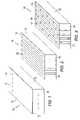
- FIGS. 1 through 11illustrate an embodiment of a process for fabricating an anti-tampering mesh on an electronic device 10 .
- terminals 12are created on a first dielectric layer 13 , which covers all surfaces of the electronic device 10 .
- the terminals 12facilitate an electrical connection from the circuits (not shown) that are contained on or in the device 10 to an anti-tampering mesh that is fabricated on the device 10 as described hereinbelow.
- the terminals 12are masked and the device 10 is coated with a first insulator layer 18 .
- Conductive traces 20are then developed on surfaces 14 , 16 to facilitate an electrical connection from the circuits (not shown) that are contained on or in the device 10 to an anti-tampering mesh that is fabricated on the device 10 as described herein.
- conductive patterns 24such as, for example, conductive polymer patterns, are deposited using, for example, an inkjet printer 26 .
- the inkjet printer 26may be, for example, a step-repeat inkjet type of thick film printer or rotary head printer.
- the device 10may be rotated in, for example, the direction of the arrow 28 so that four sides of the device 10 may have conductive patterns 24 deposited thereon.
- the conductive patterns 24are cured by, for example, a UV light source 30 .
- the UV light source 30may be attached to the inkjet printer 26 such that the conductive patterns 24 are cured upon deposition by the inkjet printer 26 .
- the resulting device 10is shown in FIG. 5 .
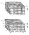
- the terminals 12are masked and the device 10 is coated with a third insulator layer 32 .
- the masksare then removed.
- the device 10is rotated ninety degrees and conductive patterns 34 , such as conductive polymer patterns, are deposited using, for example, the inkjet printer 30 .
- the device 10may be rotated in, for example, the direction of the arrow 36 so that four sides of the device 10 have conductive patterns 34 deposited thereon.
- the conductive patterns 34may be cured by, for example, the UV light source 30 .
- the light source 30may be attached to the inkjet printer 26 such that the conductive patterns 34 are cured upon deposition by the inkjet printer 26 .
- the resulting device 10is shown in FIG. 8 .
- the terminals 12are masked and the device 10 is coated with a fourth insulator layer 38 .
- the masksare then removed.
- device 10is rotated ninety degrees and conductive patterns 40 , such as conductive polymer patterns, are deposited using, for example, the inkjet printer 30 .
- the device 10may be rotated such that four sides of the device 10 may have conductive patterns 40 deposited thereon.
- the conductive patterns 40may be cured by, for example, the UV light source 30 .
- the light source 30may be attached to the inkjet printer 26 such that the conductive patterns 40 are cured upon deposition by the inkjet printer 26 .
- the terminals 12are masked and the device 10 is coated with a fifth insulator layer 42 . The masks are then removed.
- Various embodiments of the present inventionmay include conductive materials for the various conductor patterns such as, for example, UV curable conductive polymers such as Ablelux HGA-3A, photo-imagable conductive polymers, heat cured conductive polymers, Papinol's polyaniline based inks, and/or silver, gold, aluminum, or Pd/Pt evaporated coatings.
- Various embodiments of the present inventionmay include dielectric materials such as, for example, photo-imagable photoresist such as Cyclotene (BCB) 4024-40, UV curable materials such as Dupont BQ411, UV solder masks such as Lite Fast SR-1000, and/or elastomeric dielectric materials.
- the meshmay be constructed using various techniques that employ UV conductive polymers, and/or photo-imagable conductor polymers, evaporated coatings (thermal spray) of metals using, for example, e-beam technology or thermal or magnetron (sputtering) in conjunction with masks.
- the conductive tracescan also be dispensed by depositing metal-filled or carbon-filled epoxies or other filled or otherwise conductive polymers by various syringe dispensing, screen printing and like methods.
- the terminals 12may be located randomly on any number of surfaces of the device 10 .
- the conductive tracesmay be formed in any suitable shape or pattern and be arranged in any suitable orientation.
- the dielectric (non-conductive) layerscan be dispensed by various printing, syringe dispensing, coating, or fluid dispensing methods. Numerous such methods should be obvious to one of average skill in the art.
- a resistance value of a mesh that is located on the devicemay be known after the mesh is formed on the device.
- the resistancemay be monitored by, for example, a circuit located in the device and, if one or more of the lines of the mesh is broken or disrupted, a change in resistance can be detected by the circuit.
- a circuitmay be, for example, a wheatstone bridge circuit.
- the mesh circuitrymay also be monitored for changes in the capacitance of the network. In this case, it may also be possible to use the system of conducting mesh and dielectrics as a proximity detector.
- a single componentcan be replaced by multiple components, and multiple components replaced by a single component, to perform a given function or functions. Except where such substitution would not be operative to practice the present methods and systems, such substitution is within the scope of the present invention.
Landscapes
- Engineering & Computer Science (AREA)
- Microelectronics & Electronic Packaging (AREA)
- Manufacturing & Machinery (AREA)
- Computer Security & Cryptography (AREA)
- Semiconductor Integrated Circuits (AREA)
Abstract
Description
Anti-tamper (“AT”) protection is employed so that it is very difficult to reverse engineer or alter the function of electronic hardware (e.g., computer processors, integrated circuits, multi-chip modules, etc). For some commercial applications, designers often spend vast sums of money to develop a “next generation” circuit. These companies often wish to deter, or at least hamper a competitor's reverse engineering efforts. The motivation in this case is to protect valuable intellectual property. Military and Government users also have a strong interest in AT protection. When new military hardware is fielded, often the consequences of capture are not fully understood by the designer of the hardware. Similarly, the combat loss of any one of a thousand pieces of sensitive, high-tech military hardware could do irreparable damage to national security.
Most AT is categorized as either passive or active. In each case, the intent is to delay, prevent or stop tampering and potential reverse engineering of an electronic circuit. Passive AT is currently the most widespread method of deterring an opponent from reverse engineering or spoofing an electronic circuit. Current passive AT arrangements include encapsulation or various types of conformal coatings such as epoxies. Methods to defeat common encapsulants are well documented.
AT standards have been defined according to the Federal Information Protection Standard (FIPS) 140-2. The standard describes the requirements for four levels of protection. For the standards for multi-chip, embedded modules, Level 1 calls for standard passivation techniques (i.e., a sealing coat applied over the chip circuitry to protect it against environmental or other physical damage). The standard describes that Level 2 can be achieved using anti-tamper coatings or passive AT. Level 3 may use passive AT if tampering will likely destroy the module. Level 4 requires the use of active AT technologies.
Layered anti-tamper arrangements are also employed in which alternating layers of passive AT with active AT yields a synergy in probing difficulty. With active AT methods, a protected circuit will take some action when unauthorized activities are detected. Any number of events can trigger a programmed circuit response. Examples of active triggering arrangements include: voltage, photon detection, acceleration, strain, thermal, chemical attack, and proximity or tamper-respondent enclosures. A tamper-respondent package can theoretically detect probing by proximity detection or by an external activity mutilating an active circuit, exterior to what is being protected. The response of an active AT circuit upon triggering is also widely variable. For example, zeroization may be employed in which critical memory cells or an entire die can be erased. Similarly, a response can trigger overwriting of some or all of a memory die. Another detection response is to physically obliterate a critical circuit element or elements.
In one embodiment, the present invention is directed to a method of forming an anti-tamper mesh on an electronic device. The method includes forming at least one terminal on the electronic device and forming a conductive mesh on at least one surface of the electronic device, wherein the conductive mesh is in electrical contact with the terminal, and wherein the terminal facilitates electrical conduction between the conductive mesh and an electrical detection circuit.
In one embodiment, the present invention is directed to an electronic device. The device includes a conductive mesh formed on at least one surface of the electronic device and a circuit in electrical communication with the conductive mesh, wherein tampering with the conductive mesh is detected by the circuit.
In one embodiment, the present invention is directed to an electronic device. The device includes a conductive means formed on at least one surface of the electronic device and a circuit in electrical communication with the conductive means, wherein tampering with the conductive means is detected by the electrical circuit.
Various embodiments of the present invention include an electronic device that has an anti-tampering mesh that is fabricated on the device. In various embodiments, the conductive mesh is defined by single or multiple conductive layers separated by alternating non-conductive (or dielectric) layers. The multiple conductive layers are electrically connected to the detection circuitry with the terminals by electrical vias extending through the dielectric layers. As used herein, the term “electronic device” can include, for example, any type of device or package such as a semiconductor device, an electronic package, an integrated circuit chip, device or module, an electronic or electrical substrate, a circuit board, a packaged circuit, a computer, and the like.
InFIG. 3 , theterminals 12 are masked and thedevice 10 is coated with asecond insulator layer 22. The masks are then removed. InFIG. 4 ,conductive patterns 24 such as, for example, conductive polymer patterns, are deposited using, for example, aninkjet printer 26. Theinkjet printer 26 may be, for example, a step-repeat inkjet type of thick film printer or rotary head printer. Thedevice 10 may be rotated in, for example, the direction of thearrow 28 so that four sides of thedevice 10 may haveconductive patterns 24 deposited thereon. Theconductive patterns 24 are cured by, for example, aUV light source 30. TheUV light source 30 may be attached to theinkjet printer 26 such that theconductive patterns 24 are cured upon deposition by theinkjet printer 26. Theresulting device 10 is shown inFIG. 5 .
InFIG. 6 , theterminals 12 are masked and thedevice 10 is coated with athird insulator layer 32. The masks are then removed. InFIG. 7 , thedevice 10 is rotated ninety degrees andconductive patterns 34, such as conductive polymer patterns, are deposited using, for example, theinkjet printer 30. Thedevice 10 may be rotated in, for example, the direction of thearrow 36 so that four sides of thedevice 10 haveconductive patterns 34 deposited thereon. Theconductive patterns 34 may be cured by, for example, theUV light source 30. Thelight source 30 may be attached to theinkjet printer 26 such that theconductive patterns 34 are cured upon deposition by theinkjet printer 26. Theresulting device 10 is shown inFIG. 8 .
InFIG. 9 , theterminals 12 are masked and thedevice 10 is coated with afourth insulator layer 38. The masks are then removed. InFIG. 10 ,device 10 is rotated ninety degrees andconductive patterns 40, such as conductive polymer patterns, are deposited using, for example, theinkjet printer 30. Thedevice 10 may be rotated such that four sides of thedevice 10 may haveconductive patterns 40 deposited thereon. Theconductive patterns 40 may be cured by, for example, theUV light source 30. Thelight source 30 may be attached to theinkjet printer 26 such that theconductive patterns 40 are cured upon deposition by theinkjet printer 26. InFIG. 11 , theterminals 12 are masked and thedevice 10 is coated with afifth insulator layer 42. The masks are then removed.
Various embodiments of the present invention may include conductive materials for the various conductor patterns such as, for example, UV curable conductive polymers such as Ablelux HGA-3A, photo-imagable conductive polymers, heat cured conductive polymers, Papinol's polyaniline based inks, and/or silver, gold, aluminum, or Pd/Pt evaporated coatings. Various embodiments of the present invention may include dielectric materials such as, for example, photo-imagable photoresist such as Cyclotene (BCB) 4024-40, UV curable materials such as Dupont BQ411, UV solder masks such as Lite Fast SR-1000, and/or elastomeric dielectric materials.
It can be understood that various techniques may be employed to construct a mesh on an electronic device without departing from the teachings of the present invention. For example, the mesh may be constructed using various techniques that employ UV conductive polymers, and/or photo-imagable conductor polymers, evaporated coatings (thermal spray) of metals using, for example, e-beam technology or thermal or magnetron (sputtering) in conjunction with masks. The conductive traces can also be dispensed by depositing metal-filled or carbon-filled epoxies or other filled or otherwise conductive polymers by various syringe dispensing, screen printing and like methods. Also, it can be understood that theterminals 12 may be located randomly on any number of surfaces of thedevice 10. Furthermore, it can be understood that the conductive traces may be formed in any suitable shape or pattern and be arranged in any suitable orientation. It can also be understood that the dielectric (non-conductive) layers can be dispensed by various printing, syringe dispensing, coating, or fluid dispensing methods. Numerous such methods should be obvious to one of average skill in the art.
The techniques and structures of the various embodiments of the present invention may be used to detect tampering of an electronic device. In operation and according to various embodiments of the present invention, a resistance value of a mesh that is located on the device may be known after the mesh is formed on the device. The resistance may be monitored by, for example, a circuit located in the device and, if one or more of the lines of the mesh is broken or disrupted, a change in resistance can be detected by the circuit. Such a circuit may be, for example, a wheatstone bridge circuit. The mesh circuitry may also be monitored for changes in the capacitance of the network. In this case, it may also be possible to use the system of conducting mesh and dielectrics as a proximity detector.
It is to be understood that the figures and descriptions of embodiments of the present invention have been simplified to illustrate elements that are relevant for a clear understanding of the present invention, while eliminating, for purposes of clarity, other elements. Those of ordinary skill in the art will recognize, however, that these and other elements may be desirable for practice of various aspects of the present embodiments. However, because such elements are well known in the art, and because they do not facilitate a better understanding of the present invention, a discussion of such elements is not provided herein.
It can be appreciated that, in some embodiments of the present methods and systems disclosed herein, a single component can be replaced by multiple components, and multiple components replaced by a single component, to perform a given function or functions. Except where such substitution would not be operative to practice the present methods and systems, such substitution is within the scope of the present invention.
Examples presented herein, including operational examples, are intended to illustrate potential implementations of the present method and system embodiments. It can be appreciated that such examples are intended primarily for purposes of illustration. No particular aspect or aspects of the example method, product, and/or system embodiments described herein are intended to limit the scope of the present invention.
It should be appreciated that figures presented herein are intended for illustrative purposes and are not intended as construction drawings. Omitted details and modifications or alternative embodiments are within the purview of persons of ordinary skill in the art. Furthermore, whereas particular embodiments of the invention have been described herein for the purpose of illustrating the invention and not for the purpose of limiting the same, it will be appreciated by those of ordinary skill in the art that numerous variations of the details, materials and arrangement of parts/elements/steps/functions may be made within the principle and scope of the invention without departing from the invention as described in the appended claims.
Claims (11)
1. A method of forming a conductive pattern on an electronic device, the conductive pattern to detect tampering of the electronic device, the method comprising:
forming at least one terminal on the electronic device, the electronic device comprising at least one of a semiconductor device, an integrated circuit chip, and an electronic substrate; forming a non-conductive layer on the electronic device; positioning the electronic device proximate a second device, the second device for forming the conductive pattern; and
moving at least one of the electronic device and the second device to form the conductive pattern on at least two surfaces of the electronic device with the second device, wherein the conductive pattern is formed on the non-conductive layer and comprises a plurality of conductive traces, and wherein each one of the plurality of conductive traces is formed on each one of the at least two surfaces of the electronic device and is continuous therebetween; wherein the conductive pattern is electrically connected to the at least one terminal, and wherein the at least one terminal facilitates electrical conduction between the conductive pattern and an electrical detection circuit of the electronic device.
2. The method ofclaim 1 , further comprising:
depositing a non-conductive layer between a plurality of adjacent layers of deposited conductive patterns.
3. The method ofclaim 1 , comprising curing the plurality of conductive traces with one of an infrared light source, a visible light source, and an ultraviolet light source.
4. The method ofclaim 1 , comprising thermally curing the plurality of conductive traces.
5. The method ofclaim 1 , wherein moving at least one of the electronic device and second device includes rotating the electronic device relative to the second device.
6. The method ofclaim 1 , wherein moving at least one of the electronic device and second device includes rotating the second device relative to the electronic device.
7. The method ofclaim 1 , wherein the second device comprises an inkjet printer.
8. The method ofclaim 1 , wherein the second device comprises a device for applying an evaporated coating of a metal.
9. The method ofclaim 1 , wherein the second device comprises a sputtering device.
10. The method ofclaim 1 , wherein the second device comprises a screen printing device.
11. The method ofclaim 1 , wherein the second device comprises a syringe dispensing device.
Priority Applications (4)
| Application Number | Priority Date | Filing Date | Title |
|---|---|---|---|
| US11/252,402US7640658B1 (en) | 2005-10-18 | 2005-10-18 | Methods for forming an anti-tamper pattern |
| US11/944,771US7947911B1 (en) | 2005-10-18 | 2007-11-26 | Anti-tamper mesh |
| US12/653,919US8240038B1 (en) | 2005-10-18 | 2009-12-21 | Method for forming an anti-tamper mesh |
| US13/045,348US8399781B1 (en) | 2005-10-18 | 2011-03-10 | Anti-tamper mesh |
Applications Claiming Priority (1)
| Application Number | Priority Date | Filing Date | Title |
|---|---|---|---|
| US11/252,402US7640658B1 (en) | 2005-10-18 | 2005-10-18 | Methods for forming an anti-tamper pattern |
Related Child Applications (2)
| Application Number | Title | Priority Date | Filing Date |
|---|---|---|---|
| US11/944,771DivisionUS7947911B1 (en) | 2005-10-18 | 2007-11-26 | Anti-tamper mesh |
| US12/653,919ContinuationUS8240038B1 (en) | 2005-10-18 | 2009-12-21 | Method for forming an anti-tamper mesh |
Publications (1)
| Publication Number | Publication Date |
|---|---|
| US7640658B1true US7640658B1 (en) | 2010-01-05 |
Family
ID=41460225
Family Applications (4)
| Application Number | Title | Priority Date | Filing Date |
|---|---|---|---|
| US11/252,402Active2026-06-08US7640658B1 (en) | 2005-10-18 | 2005-10-18 | Methods for forming an anti-tamper pattern |
| US11/944,771Active2027-08-21US7947911B1 (en) | 2005-10-18 | 2007-11-26 | Anti-tamper mesh |
| US12/653,919Active2026-03-10US8240038B1 (en) | 2005-10-18 | 2009-12-21 | Method for forming an anti-tamper mesh |
| US13/045,348Expired - LifetimeUS8399781B1 (en) | 2005-10-18 | 2011-03-10 | Anti-tamper mesh |
Family Applications After (3)
| Application Number | Title | Priority Date | Filing Date |
|---|---|---|---|
| US11/944,771Active2027-08-21US7947911B1 (en) | 2005-10-18 | 2007-11-26 | Anti-tamper mesh |
| US12/653,919Active2026-03-10US8240038B1 (en) | 2005-10-18 | 2009-12-21 | Method for forming an anti-tamper mesh |
| US13/045,348Expired - LifetimeUS8399781B1 (en) | 2005-10-18 | 2011-03-10 | Anti-tamper mesh |
Country Status (1)
| Country | Link |
|---|---|
| US (4) | US7640658B1 (en) |
Cited By (35)
| Publication number | Priority date | Publication date | Assignee | Title |
|---|---|---|---|---|
| US20080278217A1 (en)* | 2007-05-07 | 2008-11-13 | Infineon Technologies Ag | Protection for circuit boards |
| US7947911B1 (en) | 2005-10-18 | 2011-05-24 | Teledyne Technologies Incorporated | Anti-tamper mesh |
| EP2405540A1 (en)* | 2010-07-08 | 2012-01-11 | Keymat Technology Limited | Circuit board connector with drilling tamper detection arrangement |
| US20130250662A1 (en)* | 2012-03-26 | 2013-09-26 | Honeywell International Inc. | Tamper-resistant mram utilizing chemical alteration |
| US8586871B2 (en) | 2011-07-19 | 2013-11-19 | The Charles Stark Draper Laboratory, Inc. | Interconnect schemes, and materials and methods for producing the same |
| US20150095223A1 (en)* | 2013-09-30 | 2015-04-02 | Intelligent Data S.L. | Electronic payment device |
| CN105389528A (en)* | 2014-08-22 | 2016-03-09 | 德昌电机(深圳)有限公司 | Anti-tamper Device |
| US9554477B1 (en) | 2015-12-18 | 2017-01-24 | International Business Machines Corporation | Tamper-respondent assemblies with enclosure-to-board protection |
| US9560737B2 (en) | 2015-03-04 | 2017-01-31 | International Business Machines Corporation | Electronic package with heat transfer element(s) |
| US9555606B1 (en) | 2015-12-09 | 2017-01-31 | International Business Machines Corporation | Applying pressure to adhesive using CTE mismatch between components |
| US9578764B1 (en) | 2015-09-25 | 2017-02-21 | International Business Machines Corporation | Enclosure with inner tamper-respondent sensor(s) and physical security element(s) |
| US9591776B1 (en) | 2015-09-25 | 2017-03-07 | International Business Machines Corporation | Enclosure with inner tamper-respondent sensor(s) |
| US9858776B1 (en) | 2016-06-28 | 2018-01-02 | International Business Machines Corporation | Tamper-respondent assembly with nonlinearity monitoring |
| US9881880B2 (en) | 2016-05-13 | 2018-01-30 | International Business Machines Corporation | Tamper-proof electronic packages with stressed glass component substrate(s) |
| US9894749B2 (en) | 2015-09-25 | 2018-02-13 | International Business Machines Corporation | Tamper-respondent assemblies with bond protection |
| US9904811B2 (en) | 2016-04-27 | 2018-02-27 | International Business Machines Corporation | Tamper-proof electronic packages with two-phase dielectric fluid |
| US9913389B2 (en) | 2015-12-01 | 2018-03-06 | International Business Corporation Corporation | Tamper-respondent assembly with vent structure |
| US9911012B2 (en) | 2015-09-25 | 2018-03-06 | International Business Machines Corporation | Overlapping, discrete tamper-respondent sensors |
| US9913370B2 (en) | 2016-05-13 | 2018-03-06 | International Business Machines Corporation | Tamper-proof electronic packages formed with stressed glass |
| US9916744B2 (en) | 2016-02-25 | 2018-03-13 | International Business Machines Corporation | Multi-layer stack with embedded tamper-detect protection |
| US9924591B2 (en) | 2015-09-25 | 2018-03-20 | International Business Machines Corporation | Tamper-respondent assemblies |
| US9978231B2 (en) | 2015-10-21 | 2018-05-22 | International Business Machines Corporation | Tamper-respondent assembly with protective wrap(s) over tamper-respondent sensor(s) |
| US9999124B2 (en) | 2016-11-02 | 2018-06-12 | International Business Machines Corporation | Tamper-respondent assemblies with trace regions of increased susceptibility to breaking |
| US10098235B2 (en) | 2015-09-25 | 2018-10-09 | International Business Machines Corporation | Tamper-respondent assemblies with region(s) of increased susceptibility to damage |
| US10136519B2 (en) | 2015-10-19 | 2018-11-20 | International Business Machines Corporation | Circuit layouts of tamper-respondent sensors |
| US10172239B2 (en) | 2015-09-25 | 2019-01-01 | International Business Machines Corporation | Tamper-respondent sensors with formed flexible layer(s) |
| US10168185B2 (en) | 2015-09-25 | 2019-01-01 | International Business Machines Corporation | Circuit boards and electronic packages with embedded tamper-respondent sensor |
| US10271424B2 (en) | 2016-09-26 | 2019-04-23 | International Business Machines Corporation | Tamper-respondent assemblies with in situ vent structure(s) |
| US10299372B2 (en) | 2016-09-26 | 2019-05-21 | International Business Machines Corporation | Vented tamper-respondent assemblies |
| US10306753B1 (en) | 2018-02-22 | 2019-05-28 | International Business Machines Corporation | Enclosure-to-board interface with tamper-detect circuit(s) |
| US10321589B2 (en) | 2016-09-19 | 2019-06-11 | International Business Machines Corporation | Tamper-respondent assembly with sensor connection adapter |
| US10327343B2 (en) | 2015-12-09 | 2019-06-18 | International Business Machines Corporation | Applying pressure to adhesive using CTE mismatch between components |
| US10327329B2 (en) | 2017-02-13 | 2019-06-18 | International Business Machines Corporation | Tamper-respondent assembly with flexible tamper-detect sensor(s) overlying in-situ-formed tamper-detect sensor |
| US10426037B2 (en) | 2015-07-15 | 2019-09-24 | International Business Machines Corporation | Circuitized structure with 3-dimensional configuration |
| US11122682B2 (en) | 2018-04-04 | 2021-09-14 | International Business Machines Corporation | Tamper-respondent sensors with liquid crystal polymer layers |
Families Citing this family (16)
| Publication number | Priority date | Publication date | Assignee | Title |
|---|---|---|---|---|
| US20100171202A1 (en)* | 2009-01-07 | 2010-07-08 | Tian Weicheng | Method of securely data protecting arrangement for electronic device |
| US8896086B1 (en)* | 2013-05-30 | 2014-11-25 | Freescale Semiconductor, Inc. | System for preventing tampering with integrated circuit |
| US9997492B2 (en) | 2013-11-21 | 2018-06-12 | Nxp Usa, Inc. | Optically-masked microelectronic packages and methods for the fabrication thereof |
| US9392734B1 (en) | 2014-02-11 | 2016-07-12 | Lockheed Martin Corporation | Security wrapper for an electronic assembly and methods for forming such a wrapper |
| CN105891651B (en) | 2015-01-16 | 2019-12-10 | 恩智浦美国有限公司 | Low power open circuit detection system |
| US10007811B2 (en) | 2015-02-25 | 2018-06-26 | Private Machines Inc. | Anti-tamper system |
| US9455233B1 (en) | 2015-12-02 | 2016-09-27 | Freescale Semiconductor, Inc. | System for preventing tampering with integrated circuit |
| US10678958B2 (en) | 2015-12-28 | 2020-06-09 | Intelligent Technologies International, Inc. | Intrusion-protected memory component |
| US9887847B2 (en) | 2016-02-03 | 2018-02-06 | International Business Machines Corporation | Secure crypto module including conductor on glass security layer |
| JP6945736B2 (en) | 2017-11-02 | 2021-10-06 | レイセオン カンパニー | Multi-GHz guard sensor for detecting physical or electromagnetic intrusion in the guard area |
| US10740499B2 (en) | 2018-03-12 | 2020-08-11 | Nuvoton Technology Corporation | Active shield portion serving as serial keypad |
| EP3550466B1 (en) | 2018-04-06 | 2023-08-02 | Fraunhofer-Gesellschaft zur Förderung der angewandten Forschung e.V. | Puf-film and method for producing the same |
| EP3550475A1 (en) | 2018-04-06 | 2019-10-09 | Fraunhofer-Gesellschaft zur Förderung der angewandten Forschung e.V. | Puf-film and method for producing the same |
| EP3550623B1 (en) | 2018-04-06 | 2020-07-29 | Fraunhofer-Gesellschaft zur Förderung der angewandten Forschung e.V. | Puf-film and method for producing the same |
| US10490507B1 (en)* | 2018-05-31 | 2019-11-26 | Loomia Technologies, Inc. | Electronic components for soft, flexible circuitry layers and methods therefor |
| US11877390B2 (en) | 2021-08-30 | 2024-01-16 | International Business Machines Corporation | Fabricating tamper-respondent sensors with random three-dimensional security patterns |
Citations (15)
| Publication number | Priority date | Publication date | Assignee | Title |
|---|---|---|---|---|
| US3725671A (en) | 1970-11-02 | 1973-04-03 | Us Navy | Pyrotechnic eradication of microcircuits |
| US3860835A (en) | 1971-02-10 | 1975-01-14 | Us Navy | Anti-compromise microelectronic circuit |
| US4175990A (en) | 1977-06-27 | 1979-11-27 | Nippon Oil And Fats Co., Ltd. | Water-gel explosive and a method of producing the same |
| US4962415A (en) | 1986-12-15 | 1990-10-09 | Hitachi Maxell, Ltd. | IC card |
| US5027397A (en)* | 1989-09-12 | 1991-06-25 | International Business Machines Corporation | Data protection by detection of intrusion into electronic assemblies |
| US5233505A (en)* | 1991-12-30 | 1993-08-03 | Yeng-Ming Chang | Security device for protecting electronically-stored data |
| US5858500A (en)* | 1993-03-12 | 1999-01-12 | W. L. Gore & Associates, Inc. | Tamper respondent enclosure |
| US5861662A (en)* | 1997-02-24 | 1999-01-19 | General Instrument Corporation | Anti-tamper bond wire shield for an integrated circuit |
| US6201707B1 (en) | 1998-05-28 | 2001-03-13 | Sharp Kabushiki Kaisha | Wiring substrate used for a resin-sealing type semiconductor device and a resin-sealing type semiconductor device structure using such a wiring substrate |
| US20020199111A1 (en)* | 2001-02-16 | 2002-12-26 | Clark Dereck B. | Methods and apparatus for preventing reverse-engineering of integrated circuits |
| US6524462B1 (en)* | 1998-04-06 | 2003-02-25 | Technology Development Associate Operations Limited | Method of providing conductive tracks on a printed circuit and apparatus for use in carrying out the method |
| DE10252329A1 (en) | 2002-11-11 | 2004-05-27 | Giesecke & Devrient Gmbh | Security chip, especially for a chip card, has a protection arrangement that is triggered by an applied pressure that causes two chemical reagents to come into contact thus directly or indirectly destroying secret memory contents |
| US20040244889A1 (en) | 2002-12-10 | 2004-12-09 | The Regents Of The University Of California | Porous silicon-based explosive |
| US6930023B2 (en) | 2000-05-16 | 2005-08-16 | Shin-Etsu Handotai Co, Ltd. | Semiconductor wafer thinning method, and thin semiconductor wafer |
| US7489013B1 (en) | 2005-10-17 | 2009-02-10 | Teledyne Technologies Incorporated | Destructor integrated circuit chip, interposer electronic device and methods |
Family Cites Families (18)
| Publication number | Priority date | Publication date | Assignee | Title |
|---|---|---|---|---|
| US4860351A (en)* | 1986-11-05 | 1989-08-22 | Ibm Corporation | Tamper-resistant packaging for protection of information stored in electronic circuitry |
| EP0396869A1 (en)* | 1989-05-09 | 1990-11-14 | Thomas Matouschek | Alarm device for surface protection |
| US5389738A (en)* | 1992-05-04 | 1995-02-14 | Motorola, Inc. | Tamperproof arrangement for an integrated circuit device |
| US5503992A (en) | 1993-09-07 | 1996-04-02 | Washington University | DNA encoding the 15kD outer membrane protein of Haemophilus influenzae |
| WO2001059544A2 (en)* | 2000-02-14 | 2001-08-16 | Rainbow Technologies B.V., Netherlands | Security module system, apparatus and process |
| US7007171B1 (en)* | 2000-09-01 | 2006-02-28 | International Business Machines Corporaton | Method and apparatus for improved fold retention on a security enclosure |
| US6982642B1 (en)* | 2000-11-20 | 2006-01-03 | International Business Machines Corporation | Security cloth design and assembly |
| US6946960B2 (en)* | 2002-12-28 | 2005-09-20 | Pitney Bowes Inc. | Active tamper detection system for electronic modules |
| US7180008B2 (en)* | 2004-01-23 | 2007-02-20 | Pitney Bowes Inc. | Tamper barrier for electronic device |
| US6996953B2 (en)* | 2004-01-23 | 2006-02-14 | Pitney Bowes Inc. | System and method for installing a tamper barrier wrap in a PCB assembly, including a PCB assembly having improved heat sinking |
| GB2412996B (en)* | 2004-04-08 | 2008-11-12 | Gore & Ass | Tamper respondent covering |
| US7156233B2 (en)* | 2004-06-15 | 2007-01-02 | Pitney Bowes Inc. | Tamper barrier enclosure with corner protection |
| US7256692B2 (en)* | 2004-12-23 | 2007-08-14 | Lockheed Martin Corporation | Anti-tamper apparatus |
| US7705439B2 (en) | 2005-01-25 | 2010-04-27 | Teledyne Technologies Incorporated | Destructor integrated circuit chip, interposer electronic device and methods |
| US7880248B1 (en) | 2005-10-17 | 2011-02-01 | Teledyne Technologies Incorporated | Destructor integrated circuit chip, interposer electronic device and methods |
| US7640658B1 (en) | 2005-10-18 | 2010-01-05 | Teledyne Technologies Incorporated | Methods for forming an anti-tamper pattern |
| US7760086B2 (en)* | 2006-11-03 | 2010-07-20 | Gore Enterprise Holdings, Inc | Tamper respondent sensor and enclosure |
| US7787256B2 (en)* | 2007-08-10 | 2010-08-31 | Gore Enterprise Holdings, Inc. | Tamper respondent system |
- 2005
- 2005-10-18USUS11/252,402patent/US7640658B1/enactiveActive
- 2007
- 2007-11-26USUS11/944,771patent/US7947911B1/enactiveActive
- 2009
- 2009-12-21USUS12/653,919patent/US8240038B1/enactiveActive
- 2011
- 2011-03-10USUS13/045,348patent/US8399781B1/ennot_activeExpired - Lifetime
Patent Citations (15)
| Publication number | Priority date | Publication date | Assignee | Title |
|---|---|---|---|---|
| US3725671A (en) | 1970-11-02 | 1973-04-03 | Us Navy | Pyrotechnic eradication of microcircuits |
| US3860835A (en) | 1971-02-10 | 1975-01-14 | Us Navy | Anti-compromise microelectronic circuit |
| US4175990A (en) | 1977-06-27 | 1979-11-27 | Nippon Oil And Fats Co., Ltd. | Water-gel explosive and a method of producing the same |
| US4962415A (en) | 1986-12-15 | 1990-10-09 | Hitachi Maxell, Ltd. | IC card |
| US5027397A (en)* | 1989-09-12 | 1991-06-25 | International Business Machines Corporation | Data protection by detection of intrusion into electronic assemblies |
| US5233505A (en)* | 1991-12-30 | 1993-08-03 | Yeng-Ming Chang | Security device for protecting electronically-stored data |
| US5858500A (en)* | 1993-03-12 | 1999-01-12 | W. L. Gore & Associates, Inc. | Tamper respondent enclosure |
| US5861662A (en)* | 1997-02-24 | 1999-01-19 | General Instrument Corporation | Anti-tamper bond wire shield for an integrated circuit |
| US6524462B1 (en)* | 1998-04-06 | 2003-02-25 | Technology Development Associate Operations Limited | Method of providing conductive tracks on a printed circuit and apparatus for use in carrying out the method |
| US6201707B1 (en) | 1998-05-28 | 2001-03-13 | Sharp Kabushiki Kaisha | Wiring substrate used for a resin-sealing type semiconductor device and a resin-sealing type semiconductor device structure using such a wiring substrate |
| US6930023B2 (en) | 2000-05-16 | 2005-08-16 | Shin-Etsu Handotai Co, Ltd. | Semiconductor wafer thinning method, and thin semiconductor wafer |
| US20020199111A1 (en)* | 2001-02-16 | 2002-12-26 | Clark Dereck B. | Methods and apparatus for preventing reverse-engineering of integrated circuits |
| DE10252329A1 (en) | 2002-11-11 | 2004-05-27 | Giesecke & Devrient Gmbh | Security chip, especially for a chip card, has a protection arrangement that is triggered by an applied pressure that causes two chemical reagents to come into contact thus directly or indirectly destroying secret memory contents |
| US20040244889A1 (en) | 2002-12-10 | 2004-12-09 | The Regents Of The University Of California | Porous silicon-based explosive |
| US7489013B1 (en) | 2005-10-17 | 2009-02-10 | Teledyne Technologies Incorporated | Destructor integrated circuit chip, interposer electronic device and methods |
Non-Patent Citations (14)
| Title |
|---|
| D3 Tamper Respondent Systems Product Brochure, 2001, 6 pages. |
| D3 Technology Tamper Respondent Sensors and Enclosures, W.L. Gore & Associates (UK) Ltd. Dundee Technology Park, Dundee DD2 1JA, Scotland, 2 pages. |
| Office Action issued on Apr. 16, 2008 in U.S. Appl. No. 11/252,403. |
| Office Action issued on Feb. 20, 2007 in U.S. Appl. No. 11/252,403. |
| Office Action issued on Jan. 7, 2009 in U.S. Appl. No. 11/043,626. |
| Office Action issued on Jun. 26, 2007 in U.S. Appl. No. 11/043,626. |
| Office Action issued on Mar. 11, 2008 in U.S. Appl. No. 11/043,626. |
| Office Action issued on Mar. 5, 2007 in U.S. Appl. No. 11/043,626. |
| Office Action issued on Oct. 13, 2006 in U.S. Appl. No. 11/252,403. |
| Office Action issued on Oct. 18, 2007 in U.S. Appl. No. 11/252,403. |
| Pyrofuze(R), Sigmund Cohn Corp., Mount Vernon, New York, printed from http://www.sigmundcohn.com/pyrofuse.html, 2 pages. |
| U.S. Appl. No. 11/043,626, filed Jan. 25, 2005. |
| U.S. Appl. No. 11/252,403, filed Oct. 17, 2005. |
| U.S. Appl. No. 11/944,771, filed Nov 26, 2007. |
Cited By (77)
| Publication number | Priority date | Publication date | Assignee | Title |
|---|---|---|---|---|
| US7947911B1 (en) | 2005-10-18 | 2011-05-24 | Teledyne Technologies Incorporated | Anti-tamper mesh |
| US8399781B1 (en) | 2005-10-18 | 2013-03-19 | Teledyne Technologies Incorporated | Anti-tamper mesh |
| US8522051B2 (en)* | 2007-05-07 | 2013-08-27 | Infineon Technologies Ag | Protection for circuit boards |
| US20080278217A1 (en)* | 2007-05-07 | 2008-11-13 | Infineon Technologies Ag | Protection for circuit boards |
| EP2405540A1 (en)* | 2010-07-08 | 2012-01-11 | Keymat Technology Limited | Circuit board connector with drilling tamper detection arrangement |
| US8137139B2 (en) | 2010-07-08 | 2012-03-20 | Keymat Technology Limited | Circuit board connector with drilling tamper detection arrangement |
| US8586871B2 (en) | 2011-07-19 | 2013-11-19 | The Charles Stark Draper Laboratory, Inc. | Interconnect schemes, and materials and methods for producing the same |
| US20130250662A1 (en)* | 2012-03-26 | 2013-09-26 | Honeywell International Inc. | Tamper-resistant mram utilizing chemical alteration |
| US8730715B2 (en)* | 2012-03-26 | 2014-05-20 | Honeywell International Inc. | Tamper-resistant MRAM utilizing chemical alteration |
| US9489668B2 (en)* | 2013-09-30 | 2016-11-08 | Flypos, S.L. | Electronic payment device |
| US20150095223A1 (en)* | 2013-09-30 | 2015-04-02 | Intelligent Data S.L. | Electronic payment device |
| CN105389528B (en)* | 2014-08-22 | 2019-11-12 | 德昌电机(深圳)有限公司 | Anti- intrusion equipment |
| CN105389528A (en)* | 2014-08-22 | 2016-03-09 | 德昌电机(深圳)有限公司 | Anti-tamper Device |
| US9560737B2 (en) | 2015-03-04 | 2017-01-31 | International Business Machines Corporation | Electronic package with heat transfer element(s) |
| US10237964B2 (en) | 2015-03-04 | 2019-03-19 | International Business Machines Corporation | Manufacturing electronic package with heat transfer element(s) |
| US10524362B2 (en) | 2015-07-15 | 2019-12-31 | International Business Machines Corporation | Circuitized structure with 3-dimensional configuration |
| US10426037B2 (en) | 2015-07-15 | 2019-09-24 | International Business Machines Corporation | Circuitized structure with 3-dimensional configuration |
| US9913362B2 (en) | 2015-09-25 | 2018-03-06 | International Business Machines Corporation | Tamper-respondent assemblies with bond protection |
| US10378925B2 (en) | 2015-09-25 | 2019-08-13 | International Business Machines Corporation | Circuit boards and electronic packages with embedded tamper-respondent sensor |
| US10624202B2 (en) | 2015-09-25 | 2020-04-14 | International Business Machines Corporation | Tamper-respondent assemblies with bond protection |
| US10271434B2 (en) | 2015-09-25 | 2019-04-23 | International Business Machines Corporation | Method of fabricating a tamper-respondent assembly with region(s) of increased susceptibility to damage |
| US9591776B1 (en) | 2015-09-25 | 2017-03-07 | International Business Machines Corporation | Enclosure with inner tamper-respondent sensor(s) |
| US9894749B2 (en) | 2015-09-25 | 2018-02-13 | International Business Machines Corporation | Tamper-respondent assemblies with bond protection |
| US10395067B2 (en) | 2015-09-25 | 2019-08-27 | International Business Machines Corporation | Method of fabricating a tamper-respondent sensor assembly |
| US10175064B2 (en) | 2015-09-25 | 2019-01-08 | International Business Machines Corporation | Circuit boards and electronic packages with embedded tamper-respondent sensor |
| US9913416B2 (en) | 2015-09-25 | 2018-03-06 | International Business Machines Corporation | Enclosure with inner tamper-respondent sensor(s) and physical security element(s) |
| US10685146B2 (en) | 2015-09-25 | 2020-06-16 | International Business Machines Corporation | Overlapping, discrete tamper-respondent sensors |
| US9911012B2 (en) | 2015-09-25 | 2018-03-06 | International Business Machines Corporation | Overlapping, discrete tamper-respondent sensors |
| US9717154B2 (en) | 2015-09-25 | 2017-07-25 | International Business Machines Corporation | Enclosure with inner tamper-respondent sensor(s) |
| US10378924B2 (en) | 2015-09-25 | 2019-08-13 | International Business Machines Corporation | Circuit boards and electronic packages with embedded tamper-respondent sensor |
| US9924591B2 (en) | 2015-09-25 | 2018-03-20 | International Business Machines Corporation | Tamper-respondent assemblies |
| US9936573B2 (en) | 2015-09-25 | 2018-04-03 | International Business Machines Corporation | Tamper-respondent assemblies |
| US10257939B2 (en) | 2015-09-25 | 2019-04-09 | International Business Machines Corporation | Method of fabricating tamper-respondent sensor |
| US10331915B2 (en) | 2015-09-25 | 2019-06-25 | International Business Machines Corporation | Overlapping, discrete tamper-respondent sensors |
| US10098235B2 (en) | 2015-09-25 | 2018-10-09 | International Business Machines Corporation | Tamper-respondent assemblies with region(s) of increased susceptibility to damage |
| US10334722B2 (en) | 2015-09-25 | 2019-06-25 | International Business Machines Corporation | Tamper-respondent assemblies |
| US9578764B1 (en) | 2015-09-25 | 2017-02-21 | International Business Machines Corporation | Enclosure with inner tamper-respondent sensor(s) and physical security element(s) |
| US10264665B2 (en) | 2015-09-25 | 2019-04-16 | International Business Machines Corporation | Tamper-respondent assemblies with bond protection |
| US10178818B2 (en) | 2015-09-25 | 2019-01-08 | International Business Machines Corporation | Enclosure with inner tamper-respondent sensor(s) and physical security element(s) |
| US10168185B2 (en) | 2015-09-25 | 2019-01-01 | International Business Machines Corporation | Circuit boards and electronic packages with embedded tamper-respondent sensor |
| US10172239B2 (en) | 2015-09-25 | 2019-01-01 | International Business Machines Corporation | Tamper-respondent sensors with formed flexible layer(s) |
| US10136519B2 (en) | 2015-10-19 | 2018-11-20 | International Business Machines Corporation | Circuit layouts of tamper-respondent sensors |
| US10143090B2 (en) | 2015-10-19 | 2018-11-27 | International Business Machines Corporation | Circuit layouts of tamper-respondent sensors |
| US9978231B2 (en) | 2015-10-21 | 2018-05-22 | International Business Machines Corporation | Tamper-respondent assembly with protective wrap(s) over tamper-respondent sensor(s) |
| US9913389B2 (en) | 2015-12-01 | 2018-03-06 | International Business Corporation Corporation | Tamper-respondent assembly with vent structure |
| US10251288B2 (en) | 2015-12-01 | 2019-04-02 | International Business Machines Corporation | Tamper-respondent assembly with vent structure |
| US10327343B2 (en) | 2015-12-09 | 2019-06-18 | International Business Machines Corporation | Applying pressure to adhesive using CTE mismatch between components |
| US9555606B1 (en) | 2015-12-09 | 2017-01-31 | International Business Machines Corporation | Applying pressure to adhesive using CTE mismatch between components |
| US10172232B2 (en) | 2015-12-18 | 2019-01-01 | International Business Machines Corporation | Tamper-respondent assemblies with enclosure-to-board protection |
| US9554477B1 (en) | 2015-12-18 | 2017-01-24 | International Business Machines Corporation | Tamper-respondent assemblies with enclosure-to-board protection |
| US9661747B1 (en) | 2015-12-18 | 2017-05-23 | International Business Machines Corporation | Tamper-respondent assemblies with enclosure-to-board protection |
| US9877383B2 (en) | 2015-12-18 | 2018-01-23 | International Business Machines Corporation | Tamper-respondent assemblies with enclosure-to-board protection |
| US10169967B1 (en) | 2016-02-25 | 2019-01-01 | International Business Machines Corporation | Multi-layer stack with embedded tamper-detect protection |
| US10217336B2 (en) | 2016-02-25 | 2019-02-26 | International Business Machines Corporation | Multi-layer stack with embedded tamper-detect protection |
| US10169968B1 (en) | 2016-02-25 | 2019-01-01 | International Business Machines Corporation | Multi-layer stack with embedded tamper-detect protection |
| US9916744B2 (en) | 2016-02-25 | 2018-03-13 | International Business Machines Corporation | Multi-layer stack with embedded tamper-detect protection |
| US10115275B2 (en) | 2016-02-25 | 2018-10-30 | International Business Machines Corporation | Multi-layer stack with embedded tamper-detect protection |
| US10169624B2 (en) | 2016-04-27 | 2019-01-01 | International Business Machines Corporation | Tamper-proof electronic packages with two-phase dielectric fluid |
| US9904811B2 (en) | 2016-04-27 | 2018-02-27 | International Business Machines Corporation | Tamper-proof electronic packages with two-phase dielectric fluid |
| US10535618B2 (en) | 2016-05-13 | 2020-01-14 | International Business Machines Corporation | Tamper-proof electronic packages with stressed glass component substrate(s) |
| US10257924B2 (en) | 2016-05-13 | 2019-04-09 | International Business Machines Corporation | Tamper-proof electronic packages formed with stressed glass |
| US10177102B2 (en) | 2016-05-13 | 2019-01-08 | International Business Machines Corporation | Tamper-proof electronic packages with stressed glass component substrate(s) |
| US10535619B2 (en) | 2016-05-13 | 2020-01-14 | International Business Machines Corporation | Tamper-proof electronic packages with stressed glass component substrate(s) |
| US9881880B2 (en) | 2016-05-13 | 2018-01-30 | International Business Machines Corporation | Tamper-proof electronic packages with stressed glass component substrate(s) |
| US9913370B2 (en) | 2016-05-13 | 2018-03-06 | International Business Machines Corporation | Tamper-proof electronic packages formed with stressed glass |
| US9858776B1 (en) | 2016-06-28 | 2018-01-02 | International Business Machines Corporation | Tamper-respondent assembly with nonlinearity monitoring |
| US10242543B2 (en) | 2016-06-28 | 2019-03-26 | International Business Machines Corporation | Tamper-respondent assembly with nonlinearity monitoring |
| US10321589B2 (en) | 2016-09-19 | 2019-06-11 | International Business Machines Corporation | Tamper-respondent assembly with sensor connection adapter |
| US10299372B2 (en) | 2016-09-26 | 2019-05-21 | International Business Machines Corporation | Vented tamper-respondent assemblies |
| US10271424B2 (en) | 2016-09-26 | 2019-04-23 | International Business Machines Corporation | Tamper-respondent assemblies with in situ vent structure(s) |
| US10667389B2 (en) | 2016-09-26 | 2020-05-26 | International Business Machines Corporation | Vented tamper-respondent assemblies |
| US9999124B2 (en) | 2016-11-02 | 2018-06-12 | International Business Machines Corporation | Tamper-respondent assemblies with trace regions of increased susceptibility to breaking |
| US10327329B2 (en) | 2017-02-13 | 2019-06-18 | International Business Machines Corporation | Tamper-respondent assembly with flexible tamper-detect sensor(s) overlying in-situ-formed tamper-detect sensor |
| US10306753B1 (en) | 2018-02-22 | 2019-05-28 | International Business Machines Corporation | Enclosure-to-board interface with tamper-detect circuit(s) |
| US10531561B2 (en) | 2018-02-22 | 2020-01-07 | International Business Machines Corporation | Enclosure-to-board interface with tamper-detect circuit(s) |
| US11083082B2 (en) | 2018-02-22 | 2021-08-03 | International Business Machines Corporation | Enclosure-to-board interface with tamper-detect circuit(s) |
| US11122682B2 (en) | 2018-04-04 | 2021-09-14 | International Business Machines Corporation | Tamper-respondent sensors with liquid crystal polymer layers |
Also Published As
| Publication number | Publication date |
|---|---|
| US8240038B1 (en) | 2012-08-14 |
| US7947911B1 (en) | 2011-05-24 |
| US8399781B1 (en) | 2013-03-19 |
Similar Documents
| Publication | Publication Date | Title |
|---|---|---|
| US7640658B1 (en) | Methods for forming an anti-tamper pattern | |
| US10172232B2 (en) | Tamper-respondent assemblies with enclosure-to-board protection | |
| US8659908B2 (en) | Protective circuit board cover | |
| US11083082B2 (en) | Enclosure-to-board interface with tamper-detect circuit(s) | |
| US10251288B2 (en) | Tamper-respondent assembly with vent structure | |
| US6686539B2 (en) | Tamper-responding encapsulated enclosure having flexible protective mesh structure | |
| US10321589B2 (en) | Tamper-respondent assembly with sensor connection adapter | |
| US9999124B2 (en) | Tamper-respondent assemblies with trace regions of increased susceptibility to breaking | |
| US10667389B2 (en) | Vented tamper-respondent assemblies | |
| US11191155B1 (en) | Tamper-respondent assembly with structural material within sealed inner compartment | |
| US10327329B2 (en) | Tamper-respondent assembly with flexible tamper-detect sensor(s) overlying in-situ-formed tamper-detect sensor | |
| US10271424B2 (en) | Tamper-respondent assemblies with in situ vent structure(s) | |
| US11122682B2 (en) | Tamper-respondent sensors with liquid crystal polymer layers | |
| US8637985B2 (en) | Anti-tamper wrapper interconnect method and a device | |
| US11147158B2 (en) | Tamper-respondent assembly with interconnect characteristic(s) obscuring circuit layout |
Legal Events
| Date | Code | Title | Description |
|---|---|---|---|
| AS | Assignment | Owner name:TELEDYNE TECHNOLOGIES INCORPORATED, CALIFORNIA Free format text:ASSIGNMENT OF ASSIGNORS INTEREST;ASSIGNORS:PHAM, CUONG V.;CHUBIN, DAVID E.;CLARKE, ROBERT A.;AND OTHERS;REEL/FRAME:016992/0145;SIGNING DATES FROM 20051228 TO 20060103 | |
| STCF | Information on status: patent grant | Free format text:PATENTED CASE | |
| CC | Certificate of correction | ||
| FPAY | Fee payment | Year of fee payment:4 | |
| FPAY | Fee payment | Year of fee payment:8 | |
| MAFP | Maintenance fee payment | Free format text:PAYMENT OF MAINTENANCE FEE, 12TH YEAR, LARGE ENTITY (ORIGINAL EVENT CODE: M1553); ENTITY STATUS OF PATENT OWNER: LARGE ENTITY Year of fee payment:12 | |
| AS | Assignment | Owner name:TELEDYNE BROWN ENGINEERING, INC., CALIFORNIA Free format text:ASSIGNMENT OF ASSIGNORS INTEREST;ASSIGNOR:TELEDYNE TECHNOLOGIES INCORPORATED;REEL/FRAME:064245/0025 Effective date:20230703 |