US7639861B2 - Method and apparatus for backlighting a wafer during alignment - Google Patents
Method and apparatus for backlighting a wafer during alignmentDownload PDFInfo
- Publication number
- US7639861B2 US7639861B2US11/162,540US16254005AUS7639861B2US 7639861 B2US7639861 B2US 7639861B2US 16254005 AUS16254005 AUS 16254005AUS 7639861 B2US7639861 B2US 7639861B2
- Authority
- US
- United States
- Prior art keywords
- wafer
- camera
- electroluminescent lamp
- electroluminescent
- machine vision
- Prior art date
- Legal status (The legal status is an assumption and is not a legal conclusion. Google has not performed a legal analysis and makes no representation as to the accuracy of the status listed.)
- Expired - Fee Related, expires
Links
- 238000000034methodMethods0.000titleclaimsabstractdescription25
- 239000000463materialSubstances0.000claimsabstractdescription28
- 238000005286illuminationMethods0.000claimsabstractdescription23
- 239000012636effectorSubstances0.000claimsdescription12
- 239000000758substrateSubstances0.000claimsdescription12
- 239000002131composite materialSubstances0.000claimsdescription4
- 239000011521glassSubstances0.000claimsdescription4
- 235000012431wafersNutrition0.000description82
- 238000004519manufacturing processMethods0.000description10
- XUIMIQQOPSSXEZ-UHFFFAOYSA-NSiliconChemical compound[Si]XUIMIQQOPSSXEZ-UHFFFAOYSA-N0.000description8
- 229910052710siliconInorganic materials0.000description8
- 239000010703siliconSubstances0.000description8
- 238000012545processingMethods0.000description6
- OAICVXFJPJFONN-UHFFFAOYSA-NPhosphorusChemical compound[P]OAICVXFJPJFONN-UHFFFAOYSA-N0.000description4
- 239000004065semiconductorSubstances0.000description3
- 238000010586diagramMethods0.000description2
- 230000003068static effectEffects0.000description2
- YLJREFDVOIBQDA-UHFFFAOYSA-NtacrineChemical compoundC1=CC=C2C(N)=C(CCCC3)C3=NC2=C1YLJREFDVOIBQDA-UHFFFAOYSA-N0.000description2
- 229960001685tacrineDrugs0.000description2
- 239000004593EpoxySubstances0.000description1
- 239000000853adhesiveSubstances0.000description1
- 230000001070adhesive effectEffects0.000description1
- XAGFODPZIPBFFR-UHFFFAOYSA-NaluminiumChemical compound[Al]XAGFODPZIPBFFR-UHFFFAOYSA-N0.000description1
- 229910052782aluminiumInorganic materials0.000description1
- 238000012993chemical processingMethods0.000description1
- 239000003086colorantSubstances0.000description1
- 238000010276constructionMethods0.000description1
- 239000013078crystalSubstances0.000description1
- 230000001351cycling effectEffects0.000description1
- 230000001419dependent effectEffects0.000description1
- 238000009434installationMethods0.000description1
- 238000007737ion beam depositionMethods0.000description1
- 229910021421monocrystalline siliconInorganic materials0.000description1
- 230000003287optical effectEffects0.000description1
- 230000002093peripheral effectEffects0.000description1
- 238000000206photolithographyMethods0.000description1
- 239000004033plasticSubstances0.000description1
- 239000004417polycarbonateSubstances0.000description1
- 229920000515polycarbonatePolymers0.000description1
- 239000010453quartzSubstances0.000description1
- VYPSYNLAJGMNEJ-UHFFFAOYSA-Nsilicon dioxideInorganic materialsO=[Si]=OVYPSYNLAJGMNEJ-UHFFFAOYSA-N0.000description1
- 239000011800void materialSubstances0.000description1
Images


Classifications
- H—ELECTRICITY
- H01—ELECTRIC ELEMENTS
- H01L—SEMICONDUCTOR DEVICES NOT COVERED BY CLASS H10
- H01L21/00—Processes or apparatus adapted for the manufacture or treatment of semiconductor or solid state devices or of parts thereof
- H01L21/67—Apparatus specially adapted for handling semiconductor or electric solid state devices during manufacture or treatment thereof; Apparatus specially adapted for handling wafers during manufacture or treatment of semiconductor or electric solid state devices or components ; Apparatus not specifically provided for elsewhere
- H01L21/67005—Apparatus not specifically provided for elsewhere
- H01L21/67242—Apparatus for monitoring, sorting or marking
- H01L21/67259—Position monitoring, e.g. misposition detection or presence detection
- G—PHYSICS
- G03—PHOTOGRAPHY; CINEMATOGRAPHY; ANALOGOUS TECHNIQUES USING WAVES OTHER THAN OPTICAL WAVES; ELECTROGRAPHY; HOLOGRAPHY
- G03F—PHOTOMECHANICAL PRODUCTION OF TEXTURED OR PATTERNED SURFACES, e.g. FOR PRINTING, FOR PROCESSING OF SEMICONDUCTOR DEVICES; MATERIALS THEREFOR; ORIGINALS THEREFOR; APPARATUS SPECIALLY ADAPTED THEREFOR
- G03F9/00—Registration or positioning of originals, masks, frames, photographic sheets or textured or patterned surfaces, e.g. automatically
- G03F9/70—Registration or positioning of originals, masks, frames, photographic sheets or textured or patterned surfaces, e.g. automatically for microlithography
- G03F9/7003—Alignment type or strategy, e.g. leveling, global alignment
- G03F9/7007—Alignment other than original with workpiece
- G03F9/7011—Pre-exposure scan; original with original holder alignment; Prealignment, i.e. workpiece with workpiece holder
- G—PHYSICS
- G03—PHOTOGRAPHY; CINEMATOGRAPHY; ANALOGOUS TECHNIQUES USING WAVES OTHER THAN OPTICAL WAVES; ELECTROGRAPHY; HOLOGRAPHY
- G03F—PHOTOMECHANICAL PRODUCTION OF TEXTURED OR PATTERNED SURFACES, e.g. FOR PRINTING, FOR PROCESSING OF SEMICONDUCTOR DEVICES; MATERIALS THEREFOR; ORIGINALS THEREFOR; APPARATUS SPECIALLY ADAPTED THEREFOR
- G03F9/00—Registration or positioning of originals, masks, frames, photographic sheets or textured or patterned surfaces, e.g. automatically
- G03F9/70—Registration or positioning of originals, masks, frames, photographic sheets or textured or patterned surfaces, e.g. automatically for microlithography
- G03F9/7088—Alignment mark detection, e.g. TTR, TTL, off-axis detection, array detector, video detection
Definitions
- This inventionrelates to illumination of a silicon wafer when using a machine vision system to obtain alignment characteristics of the wafer.
- Silicon wafer fabricationis generally described as a series of sequential photo-chemical processing steps that create an array of semiconductor devices.
- the silicon wafer, the substrate upon which the semiconductor devices are fabricatedis a flat single monocrystal of silicon. It is typically in the shape of a circle of diameter 150 mm, 200 mm or 300 mm.
- the various wafer fabrication processing stepsrequire precise alignment of the silicon wafer. Precise alignment may be required for a particular processing step because that step depends on precise crystal alignment either for manufacturing efficacy or manufacturing repeatability such as an ion beam deposition step. Alternatively, precise alignment may be required because a particular processing step is pattern-dependent and needs to be photographically registered with one of the previous steps such as a photolithography step.
- wafersare manufactured to agreed upon standards with specific features.
- SEMI M1-0305 Specifications for Polished Monocrystalline Silicon Wafersdefines some of these standards and describes notches or flats cut into the outside perimeter of the wafer permitting wafer orientation to be determined by examination of the wafer perimeter.
- Wafer Prealignment(sometimes called Wafer Coarse Alignment) is an automated process of examining the shape of a silicon wafer and its notches, flats or other geometric shape characteristics to determine the alignment of a wafer. Alignment of the wafer means determining the position and orientation of the wafer relative to a particular coordinate system. The physical positional accuracy of such an alignment could range from a fraction of a micron to a few millimeters in position and from a few thousands of a degree to a degree or two in orientation. It is possible for some of the processing steps described above to involve creating fiducial marks on the surface of the wafer. In later processing steps, those newly created fiducial marks can also be used for wafer alignment.
- Such a wafer alignment step that uses fiducial marks on the surface of the waferis called a fine alignment step and is not the subject of this application.
- a fine alignment stepis performed to align a wafer
- a coarse alignment stepis typically performed first in order to reduce the search area of the fiducial mark.
- LED illuminationthat provides backlight illumination of the wafer.
- the LED illuminatorsrequire a diffuser that distributes the point source illumination of the LED into a wide area diffused mode of illumination proximate to the peripheral region of the wafer. While effective, the conventional illumination systems and methods become increasingly complex and expensive as the wafer fabrication industry continues in its trend toward larger wafer sizes.
- the inventionprovides a method and apparatus for backlighting a wafer during wafer alignment processing.
- the inventionprovides illumination using a sheet of electroluminescent material to backlight a wafer.
- An image of the backlit waferis acquired using a camera coupled to a machine vision system.
- the waferis positioned on a stage, and the position and orientation of the wafer can be determined from the image.
- the sheet of electroluminescent materialcan be operated while adhered to a rigid substrate and applying electrical power.
- Alternate embodiments of the inventioninclude the use of a robotic end effector to position the wafer between the electroluminescent lamp and the camera.
- the wafercan be held stationary during image acquisition, or dynamically moved through the field of view.
- the electroluminescent materialcan be operated in a strobed mode of operation by momentarily cycling the power application when the wafer is in the field of view of the camera.
- FIG. 1is an illustrative diagram of an exemplary wafer alignment system according to the present invention
- FIG. 2is an illustrative diagram of an alternative exemplary wafer alignment system according to the present invention.
- FIG. 3is a representation of an image of the wafer acquired during wafer alignment according to the present invention.
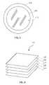
- FIG. 4is an exploded view of the electroluminescent material according to the present invention.
- FIG. 5is an isometric view of the electroluminescent lamp according to an illustrative embodiment of the present invention.
- a wafer alignment systemthat can be deployed in a wafer fabrication process for providing coarse alignment of a silicon wafer.
- a silicon wafer 100is presented to a machine vision camera 120 using an alignment stage 130 .
- An electroluminescent lamp 110projects illumination toward the camera 120 to provide backlight illumination of the wafer 100 through the application of power from a power supply 140 .
- a robot end effector or a personplaces the wafer 100 upon the alignment stage 130 .
- the wafercan be inaccurately placed on the stage and can have any orientation—the objective of the wafer alignment process is to determine the relative position and angular orientation of the wafer 100 to a reference location or position, so that an automated material transfer system, like a robotic end effector, can accurately pick up and transfer the wafer using the determined relative positional information.
- a machine vision system 150acquires at least one image of the wafer on the alignment stage using the camera 120 .
- the machine vision systemis a personal computer with a frame grabber, like the MVS-8100 PCI frame grabber available from Cognex Corporation.
- the camera 120can be an RS-170/CCIR industry standard 640 ⁇ 480 monochrome camera, coupled to the machine vision system 150 using standard video interconnection cables.
- the camera 120 and the machine vision system 150can be an integrated sensor, for example, an In-Sight 1700 Series Wafer Reader, also available from Cognex Corporation, where the functionality of the camera 120 is internally coupled to the machine vision system 150 . In a clean-room environment, the integrated camera/system solution will be preferred.
- the acquired image of the wafer 100 , backlit by the electroluminescent lamp 110is represented by FIG. 3 .
- An apparent edgeis visible in the image between the electroluminescent lamp 110 and the wafer 100 ; the lamp 110 will appear bright, while the wafer 100 will appear dark.
- a center position of the wafercan be determined.
- the angular orientation of the wafercan be determined by finding the notch 115 , using conventional pattern matching or correlation matching tools commonly known in the art.
- the notch 115may appear as a short chord feature, or “flat” in the circular profile of the wafer, though the same, or similar, feature locating methods can be similarly applied.
- One method of performing the machine vision methods for determining the position and orientation of wafer using an acquired backlit image of the waferis described in commonly assigned U.S. Pat. No. 5,825,913, the entirety of which is herein incorporated by reference.
- a robot end effector 160passes the wafer between the lamp 110 and the camera 120 so that the wafer alignment process can be performed, with the determined wafer position and orientation passed to the robot controller.
- the wafer alignment process in this embodimentis the same as that described above with reference to the camera 120 coupled to the machine vision system 150 , or through the use of an integrated sensor.
- features of the robot end effector 160typically a vacuum grip or edge grip configuration, will appear in the acquired image.
- the wafer alignment processmust be tolerant of these extraneous features, and there is the possibility that the notch or flat features may be obscured by the robot end effector 160 .
- the robot end effector 160may pause in the predetermined position so that the wafer alignment process can be performed, or the image can be acquired as the end effector 160 dynamically passes the wafer through the predetermined position.
- a strobed actuation of the lamp 110is preferred, by momentarily actuating the power supply 140 , as described below.
- FIG. 4An exploded view of a section of the electroluminescent material 112 used in the electroluminescent lamp 110 is shown in FIG. 4 .
- a thin layer of light emitting phosphor 185is placed between a translucent electrode 195 and an opaque electrode 175 .
- alternating current400-1600 Hz
- the phosphor layer 185rapidly charges and discharges, resulting in the emission of light.
- An insulating layer 165electrically isolates the active layers of the composite structure from the base structural material 155 .
- the typical thickness of the electroluminescent materialis approximately 0.30+/ ⁇ 0.03 mm.
- the electroluminescent lamp 110is fabricated by attaching the electroluminescent material 112 , which is typically flexible, to a rigid substrate 145 .
- the electroluminescent materialcan be obtained from MKS, Bridgeton, N.J., as Quantaflex 1600.
- the rigid substrate material 145can be, for example, polycarbonate, or any similar material that is suitable for use in a wafer fabrication clean-room environment, such as G10 epoxy-glass composites, or anodized aluminum.
- an adhesive suitable for use in a wafer fabrication clean-room environmentsuch as Dymax “Multi-cure 427”, UV cured epoxy.
- the illustrative embodiment of the present inventionis a circular shape in an annular ring, with a void area in the center to accommodate the wafer stage 130 .
- the lampis approximately fourteen inches in diameter overall with an six inch center diameter.
- nearly any geometric shapeis suitable for the design of the lamp 110 , so long as the expected edge of the wafer 100 is illuminated in the field of view of the camera 120 by the lamp 110 .
- the power supply 140supplies alternating current to the translucent electrode layer 195 and the opaque electrode layer 175 so that light emits from the surface of the lamp 110 .
- the power supplycontinuously applies current to the lamp 110 during image acquisition.
- the power supplycan strobe the lamp 110 with an intermittent actuation in response to a system trigger.
- the powercan be optionally overdriven according to manufacturer specification to increase illumination intensity over a short duration, at the expense of potential reduction in expected life cycle of the lamp.
- the latencyis reasonably predictable over the area of illumination, which can be calibrated with the system timing requirements.
- the electroluminescent material 112can be captured between a sheet of transparent glass, quartz, or plastic and a substrate.
- the flexible materialneed only be held relatively flat on a plane substantially parallel to the surface of the wafer under alignment so that its perceived illumination is evenly distributed over the area at the expected edge of the wafer in the field of view of the camera 120 . Since the illumination output from the material is highly efficient, the material does not generate thermal management issues with respect to the construction or particular design of the electroluminescent lamp 110 .
- the electroluminescent materialcan be obtained in any of a variety of illumination colors.
- a lime-green colorhas been selected, since it has been found to be non-reactive to semiconductor fabrication processes that are associated with, or in near proximity to, the wafer alignment processes.
- the illustrative embodimenthas been shown to be effective for wafer alignment even in installations where ambient light is not controlled. Reflection of ambient light from the lamp 110 can be distinguished from specular reflections of ambient light from the wafer under alignment by the machine vision system 150 such that sufficient contrast at the wafer edge can permit an effective analysis of an acquired image. Alternatively, a band-pass filter (not shown) that is tuned to the wavelength (color) of the light projected from electroluminescent material 112 can be installed in the optical path of the camera 120 to reduce the potential for susceptibility of ambient light reflections.
Landscapes
- Physics & Mathematics (AREA)
- General Physics & Mathematics (AREA)
- Engineering & Computer Science (AREA)
- Condensed Matter Physics & Semiconductors (AREA)
- Manufacturing & Machinery (AREA)
- Computer Hardware Design (AREA)
- Microelectronics & Electronic Packaging (AREA)
- Power Engineering (AREA)
- Multimedia (AREA)
- Electroluminescent Light Sources (AREA)
- Container, Conveyance, Adherence, Positioning, Of Wafer (AREA)
Abstract
Description
Claims (16)
Priority Applications (1)
| Application Number | Priority Date | Filing Date | Title |
|---|---|---|---|
| US11/162,540US7639861B2 (en) | 2005-09-14 | 2005-09-14 | Method and apparatus for backlighting a wafer during alignment |
Applications Claiming Priority (1)
| Application Number | Priority Date | Filing Date | Title |
|---|---|---|---|
| US11/162,540US7639861B2 (en) | 2005-09-14 | 2005-09-14 | Method and apparatus for backlighting a wafer during alignment |
Publications (2)
| Publication Number | Publication Date |
|---|---|
| US20070058168A1 US20070058168A1 (en) | 2007-03-15 |
| US7639861B2true US7639861B2 (en) | 2009-12-29 |
Family
ID=37854723
Family Applications (1)
| Application Number | Title | Priority Date | Filing Date |
|---|---|---|---|
| US11/162,540Expired - Fee RelatedUS7639861B2 (en) | 2005-09-14 | 2005-09-14 | Method and apparatus for backlighting a wafer during alignment |
Country Status (1)
| Country | Link |
|---|---|
| US (1) | US7639861B2 (en) |
Cited By (4)
| Publication number | Priority date | Publication date | Assignee | Title |
|---|---|---|---|---|
| US20080049127A1 (en)* | 2003-05-08 | 2008-02-28 | Fujifilm Corporation | Solid-state imaging device, camera module, and camera-module manufacturing method |
| US20080142604A1 (en)* | 2006-12-14 | 2008-06-19 | Laurens Nunnink | Illumination devices for image acquisition systems |
| US9819847B1 (en) | 2015-05-04 | 2017-11-14 | Harris Corporation | Uniform lighting of surfaces for visual inspection |
| US11295975B2 (en) | 2019-09-13 | 2022-04-05 | Brooks Automation Us, Llc | Method and apparatus for substrate alignment |
Families Citing this family (4)
| Publication number | Priority date | Publication date | Assignee | Title |
|---|---|---|---|---|
| TW201133691A (en)* | 2009-07-27 | 2011-10-01 | Amb App & Maschb | A test system for detecting shape and/or orientation errors of wafers |
| EP2339331A1 (en) | 2009-12-23 | 2011-06-29 | Nanda Technologies GmbH | Inspection and positioning systems and methods |
| CN118412311A (en)* | 2024-03-14 | 2024-07-30 | 深圳稳顶聚芯技术有限公司 | Wafer alignment device and method based on machine vision |
| CN118507414B (en)* | 2024-07-22 | 2024-10-11 | 苏州芯慧联半导体科技有限公司 | Wafer alignment method and device based on camera |
Citations (313)
| Publication number | Priority date | Publication date | Assignee | Title |
|---|---|---|---|---|
| US3816722A (en) | 1970-09-29 | 1974-06-11 | Nippon Electric Co | Computer for calculating the similarity between patterns and pattern recognition system comprising the similarity computer |
| US3936800A (en) | 1973-03-28 | 1976-02-03 | Hitachi, Ltd. | Pattern recognition system |
| US3967100A (en) | 1973-11-12 | 1976-06-29 | Naonobu Shimomura | Digital function generator utilizing cascade accumulation |
| US3968475A (en) | 1974-11-11 | 1976-07-06 | Sperry Rand Corporation | Digital processor for extracting data from a binary image |
| US3978326A (en) | 1974-12-27 | 1976-08-31 | Naonobu Shimomura | Digital polynomial function generator |
| US4011403A (en) | 1976-03-30 | 1977-03-08 | Northwestern University | Fiber optic laser illuminators |
| US4115762A (en) | 1976-12-01 | 1978-09-19 | Hitachi, Ltd. | Alignment pattern detecting apparatus |
| US4115702A (en) | 1976-05-05 | 1978-09-19 | Zumback Electronic Ag | Device for measuring at least one dimension of an object and a method of operating said device |
| US4183013A (en) | 1976-11-29 | 1980-01-08 | Coulter Electronics, Inc. | System for extracting shape features from an image |
| US4200861A (en) | 1978-09-01 | 1980-04-29 | View Engineering, Inc. | Pattern recognition apparatus and method |
| US4238780A (en) | 1978-04-14 | 1980-12-09 | Siemens Aktiengesellschaft | Process and an apparatus for automatically recognizing the position of semiconductor elements |
| US4254400A (en) | 1978-12-13 | 1981-03-03 | Hitachi, Ltd. | Image data processor |
| US4286293A (en) | 1979-05-30 | 1981-08-25 | Western Electric Company, Inc. | Laser scanning and multiple detection for video image processing |
| US4300164A (en) | 1980-03-21 | 1981-11-10 | View Engineering, Inc. | Adaptive video processor |
| US4385322A (en) | 1978-09-01 | 1983-05-24 | View Engineering, Inc. | Pattern recognition apparatus and method |
| US4435837A (en) | 1981-03-05 | 1984-03-06 | President And Fellows Of Harvard College | Pattern recognition and orientation system |
| US4441206A (en) | 1980-12-17 | 1984-04-03 | Hitachi, Ltd. | Pattern detecting apparatus |
| US4441124A (en) | 1981-11-05 | 1984-04-03 | Western Electric Company, Inc. | Technique for inspecting semiconductor wafers for particulate contamination |
| US4519041A (en) | 1982-05-03 | 1985-05-21 | Honeywell Inc. | Real time automated inspection |
| US4534813A (en) | 1982-07-26 | 1985-08-13 | Mcdonnell Douglas Corporation | Compound curve-flat pattern process |
| US4541116A (en) | 1984-02-27 | 1985-09-10 | Environmental Research Institute Of Mi | Neighborhood image processing stage for implementing filtering operations |
| US4545067A (en) | 1983-01-31 | 1985-10-01 | Commissariat A L'energie Atomique | Process for automatic image recognition |
| US4570180A (en) | 1982-05-28 | 1986-02-11 | International Business Machines Corporation | Method for automatic optical inspection |
| US4577344A (en) | 1983-01-17 | 1986-03-18 | Automatix Incorporated | Vision system |
| US4581762A (en) | 1984-01-19 | 1986-04-08 | Itran Corporation | Vision inspection system |
| US4606065A (en) | 1984-02-09 | 1986-08-12 | Imaging Technology Incorporated | Image processing-system |
| US4617619A (en) | 1985-10-02 | 1986-10-14 | American Sterilizer Company | Reflector for multiple source lighting fixture |
| US4630306A (en) | 1983-04-29 | 1986-12-16 | National Research Development Corp. | Apparatus and methods for coding and storing raster scan images |
| US4631750A (en) | 1980-04-11 | 1986-12-23 | Ampex Corporation | Method and system for spacially transforming images |
| US4641349A (en) | 1985-02-20 | 1987-02-03 | Leonard Flom | Iris recognition system |
| US4688088A (en) | 1984-04-20 | 1987-08-18 | Canon Kabushiki Kaisha | Position detecting device and method |
| US4697075A (en)* | 1986-04-11 | 1987-09-29 | General Electric Company | X-ray imaging system calibration using projection means |
| US4706168A (en) | 1985-11-15 | 1987-11-10 | View Engineering, Inc. | Systems and methods for illuminating objects for vision systems |
| US4707647A (en) | 1986-05-19 | 1987-11-17 | Gmf Robotics Corporation | Gray scale vision method and system utilizing same |
| US4728195A (en) | 1986-03-19 | 1988-03-01 | Cognex Corporation | Method for imaging printed circuit board component leads |
| US4730260A (en) | 1984-09-28 | 1988-03-08 | Asahi Glass Company Ltd. | Method for eyewear simulation and a device for its practice |
| US4731858A (en) | 1984-05-11 | 1988-03-15 | Siemens Aktiengesellschaft | Arrangement for the segmentation of lines |
| US4736437A (en) | 1982-11-22 | 1988-04-05 | View Engineering, Inc. | High speed pattern recognizer |
| US4742551A (en) | 1985-10-07 | 1988-05-03 | Fairchild Camera & Instrument Corporation | Multistatistics gatherer |
| US4752898A (en) | 1987-01-28 | 1988-06-21 | Tencor Instruments | Edge finding in wafers |
| US4758782A (en) | 1985-09-11 | 1988-07-19 | Kowa Company Ltd. | Method and apparatus for inspecting printed circuit board |
| US4764870A (en) | 1987-04-09 | 1988-08-16 | R.A.P.I.D., Inc. | System and method for remote presentation of diagnostic image information |
| US4771469A (en) | 1986-06-30 | 1988-09-13 | Honeywell Inc. | Means and method of representing an object shape by hierarchical boundary decomposition |
| US4776027A (en) | 1984-02-09 | 1988-10-04 | Omron Tateisi Electronics Co. | Geometric figure position and orientation detection method and device |
| US4782238A (en) | 1987-10-20 | 1988-11-01 | Eastman Kodak Company | Apparatus for generating edge position signals for use in locating an address element on a mailpiece |
| US4783829A (en) | 1983-02-23 | 1988-11-08 | Hitachi, Ltd. | Pattern recognition apparatus |
| US4783828A (en) | 1986-06-02 | 1988-11-08 | Honeywell Inc. | Two-dimensional object recognition using chain codes, histogram normalization and trellis algorithm |
| US4783826A (en) | 1986-08-18 | 1988-11-08 | The Gerber Scientific Company, Inc. | Pattern inspection system |
| US4803735A (en) | 1985-10-11 | 1989-02-07 | Hitachi, Ltd. | Method and apparatus for calculating position and orientation by combination of features of partial shapes |
| US4809077A (en) | 1986-04-22 | 1989-02-28 | Minolta Camera Kabushiki Kaisha | Solid state image sensor drive apparatus |
| US4821333A (en) | 1986-08-22 | 1989-04-11 | Environmental Research Inst. Of Michigan | Machine learning procedures for generating image domain feature detector structuring elements |
| US4831580A (en) | 1985-07-12 | 1989-05-16 | Nippon Electric Industry Co., Ltd. | Program generator |
| US4860374A (en) | 1984-04-19 | 1989-08-22 | Nikon Corporation | Apparatus for detecting position of reference pattern |
| US4860375A (en) | 1986-03-10 | 1989-08-22 | Environmental Research Inst. Of Michigan | High speed cellular processing system |
| US4876457A (en) | 1988-10-31 | 1989-10-24 | American Telephone And Telegraph Company | Method and apparatus for differentiating a planar textured surface from a surrounding background |
| US4876728A (en) | 1985-06-04 | 1989-10-24 | Adept Technology, Inc. | Vision system for distinguishing touching parts |
| EP0341122A1 (en) | 1988-05-03 | 1989-11-08 | Thomson-Csf | Matrix charge transfer photodetector having an integrated charge filtering device |
| US4891767A (en) | 1988-06-02 | 1990-01-02 | Combustion Engineering, Inc. | Machine vision system for position sensing |
| US4903218A (en) | 1987-08-13 | 1990-02-20 | Digital Equipment Corporation | Console emulation for a graphics workstation |
| US4907169A (en) | 1987-09-30 | 1990-03-06 | International Technical Associates | Adaptive tracking vision and guidance system |
| US4908874A (en) | 1980-04-11 | 1990-03-13 | Ampex Corporation | System for spatially transforming images |
| US4912659A (en) | 1987-10-30 | 1990-03-27 | International Business Machines Corporation | Parallel surface processing system for graphics display |
| US4912559A (en) | 1987-09-21 | 1990-03-27 | Kabushiki Kaisha Toshiba | Image processing method |
| US4914553A (en) | 1984-07-26 | 1990-04-03 | Sharp Kabushiki Kaisha | Lighting device |
| US4922543A (en) | 1984-12-14 | 1990-05-01 | Sten Hugo Nils Ahlbom | Image processing device |
| US4924086A (en) | 1987-11-05 | 1990-05-08 | Erwin Sick Gmbh Optik-Elektronik | Optical scanning apparatus for detecting faults on a surface |
| US4926492A (en) | 1987-07-24 | 1990-05-15 | Sharp Kabushiki Kaisha | Optical character reading apparatus and method |
| US4932065A (en) | 1988-11-16 | 1990-06-05 | Ncr Corporation | Universal character segmentation scheme for multifont OCR images |
| US4953224A (en) | 1984-09-27 | 1990-08-28 | Hitachi, Ltd. | Pattern defects detection method and apparatus |
| US4955062A (en) | 1986-12-10 | 1990-09-04 | Canon Kabushiki Kaisha | Pattern detecting method and apparatus |
| US4959898A (en) | 1990-05-22 | 1990-10-02 | Emhart Industries, Inc. | Surface mount machine with lead coplanarity verifier |
| US4962423A (en) | 1988-01-27 | 1990-10-09 | Canon Kabushiki Kaisha | Mark detecting method and apparatus |
| US4969037A (en) | 1988-08-11 | 1990-11-06 | Siemens Aktiengesellschaft | Arrangement for illuminating and detecting parts in an image processing system |
| US4972359A (en) | 1987-04-03 | 1990-11-20 | Cognex Corporation | Digital image processing system |
| US4982438A (en) | 1987-06-02 | 1991-01-01 | Hitachi, Ltd. | Apparatus and method for recognizing three-dimensional shape of object |
| US5005126A (en) | 1987-04-09 | 1991-04-02 | Prevail, Inc. | System and method for remote presentation of diagnostic image information |
| US5012433A (en) | 1987-04-27 | 1991-04-30 | International Business Machines Corporation | Multistage clipping method |
| US5012402A (en) | 1987-12-17 | 1991-04-30 | Murata Kikai Kabushiki Kaisha | System for modifying a machine's program at a remote location |
| US5012524A (en) | 1989-02-27 | 1991-04-30 | Motorola, Inc. | Automatic inspection method |
| US5027419A (en) | 1989-03-31 | 1991-06-25 | Atomic Energy Of Canada Limited | Optical images by quadrupole convolution |
| WO1991010968A1 (en) | 1990-01-11 | 1991-07-25 | Hine Design Inc. | Devices and methods for reading identification marks on semiconductor wafers |
| US5046190A (en) | 1988-09-06 | 1991-09-03 | Allen-Bradley Company, Inc. | Pipeline image processor |
| US5048094A (en) | 1988-11-29 | 1991-09-10 | Nippon Seiko Kabushiki Kaisha | Method and apparatus for checking pattern |
| US5054096A (en) | 1988-10-24 | 1991-10-01 | Empire Blue Cross/Blue Shield | Method and apparatus for converting documents into electronic data for transaction processing |
| US5060276A (en) | 1989-05-31 | 1991-10-22 | At&T Bell Laboratories | Technique for object orientation detection using a feed-forward neural network |
| US5063608A (en) | 1989-11-03 | 1991-11-05 | Datacube Inc. | Adaptive zonal coder |
| US5073958A (en) | 1989-07-15 | 1991-12-17 | U.S. Philips Corporation | Method of detecting edges in images |
| US5081689A (en) | 1989-03-27 | 1992-01-14 | Hughes Aircraft Company | Apparatus and method for extracting edges and lines |
| US5081656A (en) | 1987-10-30 | 1992-01-14 | Four Pi Systems Corporation | Automated laminography system for inspection of electronics |
| US5083073A (en) | 1990-09-20 | 1992-01-21 | Mazada Motor Manufacturing U.S.A. Corp. | Method and apparatus for calibrating a vision guided robot |
| US5086478A (en) | 1990-12-27 | 1992-02-04 | International Business Machines Corporation | Finding fiducials on printed circuit boards to sub pixel accuracy |
| US5091861A (en) | 1989-03-03 | 1992-02-25 | N.C.T. Ltd. | System for automatic finishing of machine parts |
| US5090576A (en) | 1988-12-19 | 1992-02-25 | Elbicon N.V. | Method and apparatus for sorting a flow of objects as a function of optical properties of the objects |
| US5091968A (en) | 1990-12-28 | 1992-02-25 | Ncr Corporation | Optical character recognition system and method |
| US5093867A (en) | 1987-07-22 | 1992-03-03 | Sony Corporation | Candidate article recognition with assignation of reference points and respective relative weights |
| US5115309A (en) | 1990-09-10 | 1992-05-19 | At&T Bell Laboratories | Method and apparatus for dynamic channel bandwidth allocation among multiple parallel video coders |
| US5113565A (en) | 1990-07-06 | 1992-05-19 | International Business Machines Corp. | Apparatus and method for inspection and alignment of semiconductor chips and conductive lead frames |
| EP0265302B1 (en) | 1986-09-19 | 1992-05-20 | Thomson-Csf | Fast video imaging system using an optical charge transfer sensor organised in a matrix form |
| US5119435A (en) | 1987-09-21 | 1992-06-02 | Kulicke And Soffa Industries, Inc. | Pattern recognition apparatus and method |
| US5124622A (en) | 1988-07-26 | 1992-06-23 | Fanuc Ltd. | Remote diagnosis system of numerical control apparatus |
| US5133022A (en) | 1991-02-06 | 1992-07-21 | Recognition Equipment Incorporated | Normalizing correlator for video processing |
| US5134575A (en) | 1989-12-21 | 1992-07-28 | Hitachi, Ltd. | Method of producing numerical control data for inspecting assembled printed circuit board |
| US5143436A (en) | 1991-03-06 | 1992-09-01 | The United States Of America As Represented By The United States Department Of Energy | Ringlight for use in high radiation |
| US5145432A (en) | 1991-11-27 | 1992-09-08 | Zenith Electronics Corporation | Optical interprogation system for use in constructing flat tension shadow mask CRTS |
| US5151951A (en) | 1990-03-15 | 1992-09-29 | Sharp Kabushiki Kaisha | Character recognition device which divides a single character region into subregions to obtain a character code |
| US5153925A (en) | 1989-04-27 | 1992-10-06 | Canon Kabushiki Kaisha | Image processing apparatus |
| US5155775A (en) | 1988-10-13 | 1992-10-13 | Brown C David | Structured illumination autonomous machine vision system |
| US5159645A (en) | 1988-05-12 | 1992-10-27 | Ezel Inc. | Method for recognizing concavities in an image subject to character recognition |
| US5159281A (en) | 1991-11-20 | 1992-10-27 | Nsi Partners | Digital demodulator using numerical processor to evaluate period measurements |
| US5164994A (en) | 1989-12-21 | 1992-11-17 | Hughes Aircraft Company | Solder joint locator |
| US5168269A (en) | 1990-11-08 | 1992-12-01 | Norton-Lambert Corp. | Mouse driven remote communication system |
| US5175808A (en) | 1989-09-12 | 1992-12-29 | Pixar | Method and apparatus for non-affine image warping |
| US5179419A (en) | 1991-11-22 | 1993-01-12 | At&T Bell Laboratories | Methods of detecting, classifying and quantifying defects in optical fiber end faces |
| US5185810A (en) | 1990-04-26 | 1993-02-09 | Carl-Zeiss-Stiftung | Method for optical testing of samples |
| US5185855A (en) | 1987-07-29 | 1993-02-09 | Mitsubishi Denki K.K. | Curved surface designing method |
| US5189712A (en) | 1990-07-17 | 1993-02-23 | Mitsubishi Denki K.K. | Correlation detector for images |
| US5204944A (en) | 1989-07-28 | 1993-04-20 | The Trustees Of Columbia University In The City Of New York | Separable image warping methods and systems using spatial lookup tables |
| US5206820A (en) | 1990-08-31 | 1993-04-27 | At&T Bell Laboratories | Metrology system for analyzing panel misregistration in a panel manufacturing process and providing appropriate information for adjusting panel manufacturing processes |
| US5216503A (en) | 1991-12-24 | 1993-06-01 | General Instrument Corporation | Statistical multiplexer for a multichannel image compression system |
| US5225940A (en) | 1991-03-01 | 1993-07-06 | Minolta Camera Kabushiki Kaisha | In-focus detection apparatus using video signal |
| US5230027A (en) | 1990-09-05 | 1993-07-20 | Nec Corporation | Image processor and automated optical inspection system using the same |
| US5243607A (en) | 1990-06-25 | 1993-09-07 | The Johns Hopkins University | Method and apparatus for fault tolerance |
| US5253308A (en) | 1989-06-21 | 1993-10-12 | Amber Engineering, Inc. | Massively parallel digital image data processor using pixel-mapped input/output and relative indexed addressing |
| US5253306A (en) | 1990-01-12 | 1993-10-12 | Futec Inc. | Method of matching patterns and apparatus therefor |
| US5259038A (en) | 1989-10-13 | 1993-11-02 | Hatachi, Ltd. | Point pattern matching method and system as well as picture recognizing method and system using the same |
| US5265173A (en) | 1991-03-20 | 1993-11-23 | Hughes Aircraft Company | Rectilinear object image matcher |
| US5271068A (en) | 1990-03-15 | 1993-12-14 | Sharp Kabushiki Kaisha | Character recognition device which divides a single character region into subregions to obtain a character code |
| US5287449A (en) | 1987-11-06 | 1994-02-15 | Hitachi, Ltd. | Automatic program generation method with a visual data structure display |
| US5297256A (en) | 1986-04-07 | 1994-03-22 | Crosfield Electronics (Usa) Limited | Digital image processing system and method |
| US5297238A (en) | 1991-08-30 | 1994-03-22 | Cimetrix Incorporated | Robot end-effector terminal control frame (TCF) calibration method and device |
| US5299269A (en) | 1991-12-20 | 1994-03-29 | Eastman Kodak Company | Character segmentation using an associative memory for optical character recognition |
| US5307419A (en) | 1990-11-30 | 1994-04-26 | Honda Giken Kogyo Kabushiki Kaisha | Control device of an autonomously moving body and evaluation method for data thereof |
| US5311598A (en) | 1988-10-18 | 1994-05-10 | At&T Bell Laboratories | Method and apparatus for surface inspection |
| US5315388A (en) | 1991-11-19 | 1994-05-24 | General Instrument Corporation | Multiple serial access memory for use in feedback systems such as motion compensated television |
| US5319457A (en) | 1991-09-09 | 1994-06-07 | Hitachi, Ltd. | Variable length image coding system |
| US5327156A (en) | 1990-11-09 | 1994-07-05 | Fuji Photo Film Co., Ltd. | Apparatus for processing signals representative of a computer graphics image and a real image including storing processed signals back into internal memory |
| US5329469A (en) | 1990-05-30 | 1994-07-12 | Fanuc Ltd. | Calibration method for a visual sensor |
| US5337262A (en) | 1991-12-03 | 1994-08-09 | Hr Textron Inc. | Apparatus for and method of testing hydraulic/pneumatic apparatus using computer controlled test equipment |
| US5337267A (en) | 1991-11-05 | 1994-08-09 | Sgs-Thomson Microelectronics S.A. | Squaring circuit for binary numbers |
| US5363507A (en) | 1990-08-13 | 1994-11-08 | Hitachi, Ltd. | Method and system for storing and retrieving collaboratively processed information by associated identification data |
| US5367439A (en) | 1992-12-24 | 1994-11-22 | Cognex Corporation | System for frontal illumination |
| US5367667A (en) | 1992-09-25 | 1994-11-22 | Compaq Computer Corporation | System for performing remote computer system diagnostic tests |
| US5365672A (en) | 1993-01-26 | 1994-11-22 | Mecs Corporation | Positioning apparatus for a semiconductor wafer |
| US5371836A (en) | 1988-08-24 | 1994-12-06 | Matsushita Electric Industrial Co., Ltd. | Position teaching method and control apparatus for robot |
| US5371690A (en) | 1992-01-17 | 1994-12-06 | Cognex Corporation | Method and apparatus for inspection of surface mounted devices |
| US5381004A (en) | 1993-08-31 | 1995-01-10 | Applied Materials, Inc. | Particle analysis of notched wafers |
| US5388197A (en) | 1991-08-02 | 1995-02-07 | The Grass Valley Group, Inc. | Video editing system operator inter-face for visualization and interactive control of video material |
| US5388252A (en) | 1990-09-07 | 1995-02-07 | Eastman Kodak Company | System for transparent monitoring of processors in a network with display of screen images at a remote station for diagnosis by technical support personnel |
| US5398292A (en) | 1992-04-22 | 1995-03-14 | Honda Giken Kogyo Kabushiki Kaisha | Edge detecting apparatus |
| WO1995011491A1 (en) | 1993-10-21 | 1995-04-27 | Recif | Methods and devices for identifying characters written on substrates |
| US5432525A (en) | 1989-07-26 | 1995-07-11 | Hitachi, Ltd. | Multimedia telemeeting terminal device, terminal device system and manipulation method thereof |
| US5440699A (en) | 1991-06-24 | 1995-08-08 | Compaq Computer Corporation | System by which a remote computer receives screen images from and transmits commands to a host computer |
| WO1995021376A1 (en) | 1994-02-02 | 1995-08-10 | Kratzer Automatisierung Gmbh | Device for imaging a three-dimensional object |
| WO1995022137A1 (en) | 1994-02-08 | 1995-08-17 | Cognex Corporation | Methods and apparatus for remote monitoring and control of automated video data systems |
| US5455933A (en) | 1993-07-14 | 1995-10-03 | Dell Usa, L.P. | Circuit and method for remote diagnosis of personal computers |
| US5455870A (en) | 1991-07-10 | 1995-10-03 | Raytheon Company | Apparatus and method for inspection of high component density printed circuit board |
| US5471312A (en) | 1991-07-04 | 1995-11-28 | Fanuc Ltd. | Automatic calibration method |
| US5475803A (en) | 1992-07-10 | 1995-12-12 | Lsi Logic Corporation | Method for 2-D affine transformation of images |
| US5475766A (en) | 1991-09-05 | 1995-12-12 | Kabushiki Kaisha Toshiba | Pattern inspection apparatus with corner rounding of reference pattern data |
| US5477138A (en) | 1991-07-23 | 1995-12-19 | Vlsi Technology, Inc. | Apparatus and method for testing the calibration of a variety of electronic package lead inspection systems |
| US5481712A (en) | 1993-04-06 | 1996-01-02 | Cognex Corporation | Method and apparatus for interactively generating a computer program for machine vision analysis of an object |
| US5485570A (en) | 1991-02-28 | 1996-01-16 | International Business Machines Corporation | Display station controller |
| US5491780A (en) | 1992-09-15 | 1996-02-13 | International Business Machines Corporation | System and method for efficient computer workstation screen updates |
| US5495537A (en) | 1994-06-01 | 1996-02-27 | Cognex Corporation | Methods and apparatus for machine vision template matching of images predominantly having generally diagonal and elongate features |
| US5495424A (en) | 1990-04-18 | 1996-02-27 | Matsushita Electric Industrial Co., Ltd. | Method and apparatus for inspecting solder portions |
| US5496106A (en) | 1994-12-13 | 1996-03-05 | Apple Computer, Inc. | System and method for generating a contrast overlay as a focus assist for an imaging device |
| US5497007A (en) | 1995-01-27 | 1996-03-05 | Applied Materials, Inc. | Method for automatically establishing a wafer coordinate system |
| US5500906A (en) | 1994-01-14 | 1996-03-19 | Cognex Corporation | Locating curvilinear objects using feathered fiducials |
| US5506617A (en) | 1992-12-10 | 1996-04-09 | Eastman Kodak Company | Electronic camera incorporating a computer-compatible bus interface |
| US5506682A (en) | 1982-02-16 | 1996-04-09 | Sensor Adaptive Machines Inc. | Robot vision using targets |
| US5511015A (en) | 1993-11-30 | 1996-04-23 | Loral Vought Systems Corporation | Double-accumulator implementation of the convolution function |
| US5519840A (en) | 1994-01-24 | 1996-05-21 | At&T Corp. | Method for implementing approximate data structures using operations on machine words |
| US5526050A (en) | 1994-03-31 | 1996-06-11 | Cognex Corporation | Methods and apparatus for concurrently acquiring video data from multiple video data sources |
| US5528703A (en) | 1992-02-18 | 1996-06-18 | Neopath, Inc. | Method for identifying objects using data processing techniques |
| US5532739A (en) | 1993-10-06 | 1996-07-02 | Cognex Corporation | Automated optical inspection apparatus |
| US5539409A (en) | 1994-06-30 | 1996-07-23 | Westinghouse Electric Corp. | Apparatus and method for windshear data processing |
| US5544256A (en) | 1993-10-22 | 1996-08-06 | International Business Machines Corporation | Automated defect classification system |
| US5548326A (en) | 1993-10-06 | 1996-08-20 | Cognex Corporation | Efficient image registration |
| US5550763A (en) | 1994-05-02 | 1996-08-27 | Michael; David J. | Using cone shaped search models to locate ball bonds on wire bonded devices |
| US5550888A (en) | 1994-05-06 | 1996-08-27 | U.S. Philips Corporation | Method of displaying notably a digital X-ray image as a visible image, and device for carrying out the method |
| US5553859A (en) | 1995-03-22 | 1996-09-10 | Lazer-Tron Corporation | Arcade game for sensing and validating objects |
| US5557690A (en) | 1992-12-23 | 1996-09-17 | At&T Corp. | Method and system for locating objects with subpixel precision |
| US5557410A (en) | 1994-05-26 | 1996-09-17 | Lockheed Missiles & Space Company, Inc. | Method of calibrating a three-dimensional optical measurement system |
| US5559904A (en) | 1993-10-08 | 1996-09-24 | Lucent Technologies Inc. | Method and apparatus for deriving image width and height from raw graphical image data |
| US5566877A (en) | 1995-05-01 | 1996-10-22 | Motorola Inc. | Method for inspecting a semiconductor device |
| US5568563A (en) | 1993-05-17 | 1996-10-22 | Mitsubishi Denki Kabushiki Kaisha | Method and apparatus of pattern recognition |
| US5574668A (en) | 1995-02-22 | 1996-11-12 | Beaty; Elwin M. | Apparatus and method for measuring ball grid arrays |
| US5574801A (en) | 1993-08-12 | 1996-11-12 | Collet-Beillon; Olivier | Method of inspecting an array of solder ball connections of an integrated circuit module |
| US5581632A (en) | 1994-05-02 | 1996-12-03 | Cognex Corporation | Method and apparatus for ball bond inspection system |
| US5583949A (en) | 1989-03-03 | 1996-12-10 | Hewlett-Packard Company | Apparatus and method for use in image processing |
| US5583954A (en) | 1994-03-01 | 1996-12-10 | Cognex Corporation | Methods and apparatus for fast correlation |
| US5586058A (en) | 1990-12-04 | 1996-12-17 | Orbot Instruments Ltd. | Apparatus and method for inspection of a patterned object by comparison thereof to a reference |
| US5585917A (en) | 1994-03-16 | 1996-12-17 | Gea Till Gmbh & Co. | Method and apparatus for checking containers |
| US5592562A (en) | 1994-01-19 | 1997-01-07 | International Business Machines Corporation | Inspection system for cross-sectional imaging |
| US5594859A (en) | 1992-06-03 | 1997-01-14 | Digital Equipment Corporation | Graphical user interface for video teleconferencing |
| US5598345A (en) | 1990-11-29 | 1997-01-28 | Matsushita Electric Industrial Co., Ltd. | Method and apparatus for inspecting solder portions |
| US5602937A (en) | 1994-06-01 | 1997-02-11 | Cognex Corporation | Methods and apparatus for machine vision high accuracy searching |
| US5608490A (en) | 1994-06-20 | 1997-03-04 | Nikon Corporation | Apparatus for and a method of communicating between a camera and external equipment |
| US5608872A (en) | 1993-03-19 | 1997-03-04 | Ncr Corporation | System for allowing all remote computers to perform annotation on an image and replicating the annotated image on the respective displays of other comuters |
| US5621811A (en) | 1987-10-30 | 1997-04-15 | Hewlett-Packard Co. | Learning method and apparatus for detecting and controlling solder defects |
| US5627915A (en) | 1995-01-31 | 1997-05-06 | Princeton Video Image, Inc. | Pattern recognition system employing unlike templates to detect objects having distinctive features in a video field |
| WO1997021189A1 (en) | 1995-12-06 | 1997-06-12 | Cognex Corporation | Edge peak boundary tracker |
| US5640200A (en) | 1994-08-31 | 1997-06-17 | Cognex Corporation | Golden template comparison using efficient image registration |
| US5640199A (en) | 1993-10-06 | 1997-06-17 | Cognex Corporation | Automated optical inspection apparatus |
| US5642158A (en) | 1994-05-02 | 1997-06-24 | Cognex Corporation | Method and apparatus to detect capillary indentations |
| WO1997022858A1 (en) | 1995-12-19 | 1997-06-26 | Cognex Corporation | Multiple field of view calibration plate for use in semiconductor manufacturing |
| US5647009A (en) | 1992-10-20 | 1997-07-08 | Hitachi, Ltd. | Computer aided work support system and method |
| WO1997024692A1 (en) | 1995-12-31 | 1997-07-10 | Cognex Corporation | Locating shapes in two-dimensional space curves |
| WO1997024693A1 (en) | 1996-01-02 | 1997-07-10 | Cognex Corporation | Machine vision method and apparatus for edge-based image histogram analysis |
| US5649032A (en) | 1994-11-14 | 1997-07-15 | David Sarnoff Research Center, Inc. | System for automatically aligning images to form a mosaic image |
| US5652658A (en) | 1993-10-19 | 1997-07-29 | View Engineering, Inc. | Grid array inspection system and method |
| US5657403A (en) | 1992-06-01 | 1997-08-12 | Cognex Corporation | Vision coprocessing |
| US5673334A (en) | 1995-11-30 | 1997-09-30 | Cognex Corporation | Method and apparatus for inspection of characteristics on non-rigid packages |
| US5675358A (en) | 1992-08-04 | 1997-10-07 | International Business Machines Corporation | Digital image capture control |
| US5676302A (en) | 1995-06-02 | 1997-10-14 | Cognex Corporation | Method and apparatus for crescent boundary thresholding on wire-bonded leads |
| US5684530A (en) | 1993-02-16 | 1997-11-04 | Northeast Robotics, Inc. | Continuous diffuse illumination method and apparatus |
| WO1997039416A3 (en) | 1996-04-02 | 1997-11-27 | Cognex Corp | Image formation apparatus for viewing indicia on a planar specular substrate |
| US5696848A (en) | 1995-03-09 | 1997-12-09 | Eastman Kodak Company | System for creating a high resolution image from a sequence of lower resolution motion images |
| US5715385A (en) | 1992-07-10 | 1998-02-03 | Lsi Logic Corporation | Apparatus for 2-D affine transformation of images |
| US5715369A (en) | 1995-11-27 | 1998-02-03 | Microsoft Corporation | Single processor programmable speech recognition test system |
| US5717785A (en) | 1992-01-30 | 1998-02-10 | Cognex Corporation | Method and apparatus for locating patterns in an optical image |
| US5724439A (en) | 1993-06-10 | 1998-03-03 | Matsushita Electric Industrial Co., Ltd. | Inspecting apparatus of mounted component |
| US5734807A (en) | 1994-07-21 | 1998-03-31 | Kabushiki Kaisha Sega Enterprises | Image processing devices and methods |
| EP0527632B1 (en) | 1991-08-13 | 1998-04-08 | Canon Kabushiki Kaisha | Image transmission apparatus |
| US5739846A (en) | 1996-02-05 | 1998-04-14 | Universal Instruments Corporation | Method of inspecting component placement accuracy for each first selected circuit board to be assembled of a batch |
| US5739913A (en) | 1996-08-02 | 1998-04-14 | Mrs Technology, Inc. | Non-contact edge detector |
| US5740285A (en) | 1989-12-08 | 1998-04-14 | Xerox Corporation | Image reduction/enlargement technique |
| US5742037A (en) | 1996-03-07 | 1998-04-21 | Cognex Corp. | Method and apparatus for high speed identification of objects having an identifying feature |
| US5754679A (en) | 1995-10-31 | 1998-05-19 | Cognex Corp. | Image rotating method for locating bond pads in an image |
| US5757956A (en) | 1995-10-31 | 1998-05-26 | Cognex Corp. | Template rotating method for locating bond pads in an image |
| US5761326A (en) | 1993-12-08 | 1998-06-02 | Minnesota Mining And Manufacturing Company | Method and apparatus for machine vision classification and tracking |
| US5761337A (en) | 1993-05-13 | 1998-06-02 | Sharp Kabushiki Kaisha | Method and apparatus for inspection of the appearance of bumps |
| US5768443A (en) | 1995-12-19 | 1998-06-16 | Cognex Corporation | Method for coordinating multiple fields of view in multi-camera |
| WO1998030890A1 (en) | 1997-01-06 | 1998-07-16 | Cognex Corporation | Machine vision methods and apparatus for machine vision illumination of an object |
| US5796868A (en) | 1995-12-28 | 1998-08-18 | Cognex Corporation | Object edge point filtering system for machine vision |
| US5796386A (en) | 1995-01-23 | 1998-08-18 | International Business Machines Corporation | Precise calibration procedure for sensor-based view point control system |
| US5801966A (en) | 1995-07-24 | 1998-09-01 | Cognex Corporation | Machine vision methods and articles of manufacture for determination of convex hull and convex hull angle |
| US5805722A (en) | 1993-11-22 | 1998-09-08 | Cognex Corporation | Method and apparatus for locating, inspecting, and placing large leaded devices |
| US5809658A (en) | 1993-09-29 | 1998-09-22 | Snap-On Technologies, Inc. | Method and apparatus for calibrating cameras used in the alignment of motor vehicle wheels |
| US5818443A (en) | 1996-05-06 | 1998-10-06 | Cognex Corporation | Single step coarse registration and inspection of circular objects |
| US5822055A (en) | 1995-06-06 | 1998-10-13 | Kla Instruments Corporation | Optical inspection of a specimen using multi-channel responses from the specimen using bright and darkfield detection |
| US5825913A (en) | 1995-07-18 | 1998-10-20 | Cognex Corporation | System for finding the orientation of a wafer |
| US5835099A (en) | 1996-06-26 | 1998-11-10 | Xerox Corporation | Representing a region of a color image using a space-color separable model |
| WO1998052349A1 (en) | 1997-05-15 | 1998-11-19 | Cognex Corporation | Bandwidth reduction of multichannel images for machine vision |
| US5847714A (en) | 1996-05-31 | 1998-12-08 | Hewlett Packard Company | Interpolation method and apparatus for fast image magnification |
| US5848189A (en) | 1996-03-25 | 1998-12-08 | Focus Automation Systems Inc. | Method, apparatus and system for verification of patterns |
| US5850466A (en) | 1995-02-22 | 1998-12-15 | Cognex Corporation | Golden template comparison for rotated and/or scaled images |
| WO1998059490A1 (en) | 1997-06-24 | 1998-12-30 | Cognex Corporation | Methods and apparatus for charge coupled device image acquisition with independent integration and readout |
| US5859923A (en) | 1992-12-29 | 1999-01-12 | Cognex Corporation | Mark quality inspection apparatus and method |
| US5870495A (en) | 1995-01-13 | 1999-02-09 | Sgs-Thomson Microelectronics S.R.L. | Fuzzy method and device for the recognition of geometric shapes in images |
| US5872870A (en) | 1996-02-16 | 1999-02-16 | Cognex Corporation | Machine vision methods for identifying extrema of objects in rotated reference frames |
| US5878152A (en) | 1997-05-21 | 1999-03-02 | Cognex Corporation | Depth from focal gradient analysis using object texture removal by albedo normalization |
| WO1999015864A1 (en) | 1997-09-25 | 1999-04-01 | Cognex Corporation | Machine vision methods using feedback to determine an orientation, pixel width and pixel height of a field of view |
| US5900975A (en) | 1997-10-30 | 1999-05-04 | Cognex Corporation | Ghost image extinction in an active range sensor |
| US5909504A (en) | 1996-03-15 | 1999-06-01 | Cognex Corporation | Method of testing a machine vision inspection system |
| WO1999027456A1 (en) | 1997-11-26 | 1999-06-03 | Acuity Imaging, Llc | Apparent network interface for and between embedded and host processors |
| US5912768A (en) | 1996-12-31 | 1999-06-15 | Cognex Corporation | Depth-from-defocus optical apparatus with invariance to surface reflectance properties |
| US5912984A (en) | 1996-12-19 | 1999-06-15 | Cognex Corporation | Method and apparatus for in-line solder paste inspection |
| US5918196A (en) | 1996-11-29 | 1999-06-29 | Cognex Corporation | Vision system for analyzing solid-of-revolution radius profile |
| US5933523A (en) | 1997-03-18 | 1999-08-03 | Cognex Corporation | Machine vision method and apparatus for determining the position of generally rectangular devices using boundary extracting features |
| US5949901A (en) | 1996-03-21 | 1999-09-07 | Nichani; Sanjay | Semiconductor device image inspection utilizing image subtraction and threshold imaging |
| WO1999048000A1 (en) | 1998-03-16 | 1999-09-23 | Acuity Imaging, Llc | Object oriented method of structuring a software step program |
| US5960125A (en) | 1996-11-21 | 1999-09-28 | Cognex Corporation | Nonfeedback-based machine vision method for determining a calibration relationship between a camera and a moveable object |
| US5974365A (en) | 1997-10-23 | 1999-10-26 | The United States Of America As Represented By The Secretary Of The Army | System for measuring the location and orientation of an object |
| US5974169A (en) | 1997-03-20 | 1999-10-26 | Cognex Corporation | Machine vision methods for determining characteristics of an object using boundary points and bounding regions |
| US5978502A (en) | 1996-04-01 | 1999-11-02 | Cognex Corporation | Machine vision methods for determining characteristics of three-dimensional objects |
| US5978521A (en) | 1997-09-25 | 1999-11-02 | Cognex Corporation | Machine vision methods using feedback to determine calibration locations of multiple cameras that image a common object |
| US5982132A (en) | 1997-10-09 | 1999-11-09 | Electroglas, Inc. | Rotary wafer positioning system and method |
| US6002738A (en) | 1995-07-07 | 1999-12-14 | Silicon Graphics, Inc. | System and method of performing tomographic reconstruction and volume rendering using texture mapping |
| US6002793A (en) | 1992-01-30 | 1999-12-14 | Cognex Corporation | Machine vision method and apparatus for finding an object orientation angle of a rectilinear object |
| US6016152A (en) | 1997-08-01 | 2000-01-18 | Avid Technology, Inc. | Apparatus and method for non-uniform image scaling |
| US6025905A (en) | 1996-12-31 | 2000-02-15 | Cognex Corporation | System for obtaining a uniform illumination reflectance image during periodic structured illumination |
| US6025854A (en) | 1997-12-31 | 2000-02-15 | Cognex Corporation | Method and apparatus for high speed image acquisition |
| US6026176A (en) | 1995-07-25 | 2000-02-15 | Cognex Corporation | Machine vision methods and articles of manufacture for ball grid array inspection |
| US6067379A (en) | 1988-12-09 | 2000-05-23 | Cognex Corporation | Method and apparatus for locating patterns in an optical image |
| US6069668A (en) | 1997-04-07 | 2000-05-30 | Pinnacle Systems, Inc. | System and method for producing video effects on live-action video |
| US6075881A (en) | 1997-03-18 | 2000-06-13 | Cognex Corporation | Machine vision methods for identifying collinear sets of points from an image |
| US6084631A (en) | 1995-03-24 | 2000-07-04 | Ppt Vision, Inc. | High-speed digital video serial link |
| US6118540A (en) | 1997-07-11 | 2000-09-12 | Semiconductor Technologies & Instruments, Inc. | Method and apparatus for inspecting a workpiece |
| US6137893A (en) | 1996-10-07 | 2000-10-24 | Cognex Corporation | Machine vision calibration targets and methods of determining their location and orientation in an image |
| US6141040A (en) | 1996-01-09 | 2000-10-31 | Agilent Technologies, Inc. | Measurement and inspection of leads on integrated circuit packages |
| US6170973B1 (en) | 1997-11-26 | 2001-01-09 | Cognex Corporation | Method and apparatus for wide-angle illumination in line-scanning machine vision devices |
| US6188784B1 (en) | 1996-07-12 | 2001-02-13 | American Tech Manufacturing, Inc. | Split optics arrangement for vision inspection/sorter module |
| US6191850B1 (en) | 1999-10-15 | 2001-02-20 | Cognex Corporation | System and method for inspecting an object using structured illumination |
| US6215915B1 (en) | 1998-02-20 | 2001-04-10 | Cognex Corporation | Image processing methods and apparatus for separable, general affine transformation of an image |
| US6236769B1 (en) | 1998-01-28 | 2001-05-22 | Cognex Corporation | Machine vision systems and methods for morphological transformation of an image with zero or other uniform offsets |
| US6259827B1 (en) | 1996-03-21 | 2001-07-10 | Cognex Corporation | Machine vision methods for enhancing the contrast between an object and its background using multiple on-axis images |
| US6275742B1 (en)* | 1999-04-16 | 2001-08-14 | Berkeley Process Control, Inc. | Wafer aligner system |
| US6282328B1 (en) | 1998-01-28 | 2001-08-28 | Cognex Corporation | Machine vision systems and methods for morphological transformation of an image with non-uniform offsets |
| US6298149B1 (en) | 1996-03-21 | 2001-10-02 | Cognex Corporation | Semiconductor device image inspection with contrast enhancement |
| US6341878B1 (en) | 1999-08-31 | 2002-01-29 | Cognex Corporation | Method and apparatus for providing uniform diffuse illumination to a surface |
| US6381366B1 (en) | 1998-12-18 | 2002-04-30 | Cognex Corporation | Machine vision methods and system for boundary point-based comparison of patterns and images |
| US6381375B1 (en) | 1998-02-20 | 2002-04-30 | Cognex Corporation | Methods and apparatus for generating a projection of an image |
| US6389029B1 (en) | 1998-11-10 | 2002-05-14 | Nortel Networks Limited | Local area network incorporating universal serial bus protocol |
| EP0777381B1 (en) | 1995-12-07 | 2002-07-31 | Canon Kabushiki Kaisha | Image sensing system comprising a image sensing unit and a computer |
| US6477275B1 (en) | 1999-06-16 | 2002-11-05 | Coreco Imaging, Inc. | Systems and methods for locating a pattern in an image |
| US6516092B1 (en) | 1998-05-29 | 2003-02-04 | Cognex Corporation | Robust sub-model shape-finder |
| US6639624B1 (en) | 1999-12-30 | 2003-10-28 | Cognex Corporation | Machine vision methods for inspection of leaded components |
| US6658145B1 (en) | 1997-12-31 | 2003-12-02 | Cognex Corporation | Fast high-accuracy multi-dimensional pattern inspection |
| US6684402B1 (en) | 1999-12-01 | 2004-01-27 | Cognex Technology And Investment Corporation | Control methods and apparatus for coupling multiple image acquisition devices to a digital data processor |
| US6728582B1 (en) | 2000-12-15 | 2004-04-27 | Cognex Corporation | System and method for determining the position of an object in three dimensions using a machine vision system with two cameras |
| US6748104B1 (en) | 2000-03-24 | 2004-06-08 | Cognex Corporation | Methods and apparatus for machine vision inspection using single and multiple templates or patterns |
| US6771808B1 (en) | 2000-12-15 | 2004-08-03 | Cognex Corporation | System and method for registering patterns transformed in six degrees of freedom using machine vision |
| US6850646B1 (en) | 1997-12-31 | 2005-02-01 | Cognex Corporation | Fast high-accuracy multi-dimensional pattern inspection |
| US6856698B1 (en) | 1997-11-26 | 2005-02-15 | Cognex Corporation | Fast high-accuracy multi-dimensional pattern localization |
| US6900877B2 (en) | 2002-06-12 | 2005-05-31 | Asm American, Inc. | Semiconductor wafer position shift measurement and correction |
| US6914679B2 (en) | 2001-12-18 | 2005-07-05 | Cognex Technology And Investment Corporation | Side light apparatus and method |
| US6933172B2 (en)* | 2002-02-25 | 2005-08-23 | Seiko Epson Corporation | Semiconductor wafer with spacer and its manufacturing method, semiconductor device and its manufacturing method, and circuit substrate and electronic device |
| US7006669B1 (en) | 2000-12-31 | 2006-02-28 | Cognex Corporation | Machine vision method and apparatus for thresholding images of non-uniform materials |
| US7042568B2 (en) | 2002-05-16 | 2006-05-09 | Asyst Technologies, Inc. | Pre-aligner |
| US7048400B2 (en)* | 2001-03-22 | 2006-05-23 | Lumimove, Inc. | Integrated illumination system |
| US7225734B2 (en) | 2002-05-17 | 2007-06-05 | Asys Automatisierungssysteme Gmbh | Device and method for positioning a substrate to be printed |
| US7295314B1 (en) | 1998-07-10 | 2007-11-13 | Nanometrics Incorporated | Metrology/inspection positioning system |
- 2005
- 2005-09-14USUS11/162,540patent/US7639861B2/ennot_activeExpired - Fee Related
Patent Citations (328)
| Publication number | Priority date | Publication date | Assignee | Title |
|---|---|---|---|---|
| US3816722A (en) | 1970-09-29 | 1974-06-11 | Nippon Electric Co | Computer for calculating the similarity between patterns and pattern recognition system comprising the similarity computer |
| US3936800A (en) | 1973-03-28 | 1976-02-03 | Hitachi, Ltd. | Pattern recognition system |
| US3967100A (en) | 1973-11-12 | 1976-06-29 | Naonobu Shimomura | Digital function generator utilizing cascade accumulation |
| US3968475A (en) | 1974-11-11 | 1976-07-06 | Sperry Rand Corporation | Digital processor for extracting data from a binary image |
| US3978326A (en) | 1974-12-27 | 1976-08-31 | Naonobu Shimomura | Digital polynomial function generator |
| US4011403A (en) | 1976-03-30 | 1977-03-08 | Northwestern University | Fiber optic laser illuminators |
| US4115702A (en) | 1976-05-05 | 1978-09-19 | Zumback Electronic Ag | Device for measuring at least one dimension of an object and a method of operating said device |
| US4183013A (en) | 1976-11-29 | 1980-01-08 | Coulter Electronics, Inc. | System for extracting shape features from an image |
| US4115762A (en) | 1976-12-01 | 1978-09-19 | Hitachi, Ltd. | Alignment pattern detecting apparatus |
| US4238780A (en) | 1978-04-14 | 1980-12-09 | Siemens Aktiengesellschaft | Process and an apparatus for automatically recognizing the position of semiconductor elements |
| US4385322A (en) | 1978-09-01 | 1983-05-24 | View Engineering, Inc. | Pattern recognition apparatus and method |
| US4200861A (en) | 1978-09-01 | 1980-04-29 | View Engineering, Inc. | Pattern recognition apparatus and method |
| US4254400A (en) | 1978-12-13 | 1981-03-03 | Hitachi, Ltd. | Image data processor |
| US4286293A (en) | 1979-05-30 | 1981-08-25 | Western Electric Company, Inc. | Laser scanning and multiple detection for video image processing |
| US4300164A (en) | 1980-03-21 | 1981-11-10 | View Engineering, Inc. | Adaptive video processor |
| US4631750A (en) | 1980-04-11 | 1986-12-23 | Ampex Corporation | Method and system for spacially transforming images |
| US4908874A (en) | 1980-04-11 | 1990-03-13 | Ampex Corporation | System for spatially transforming images |
| US4441206A (en) | 1980-12-17 | 1984-04-03 | Hitachi, Ltd. | Pattern detecting apparatus |
| US4435837A (en) | 1981-03-05 | 1984-03-06 | President And Fellows Of Harvard College | Pattern recognition and orientation system |
| US4441124A (en) | 1981-11-05 | 1984-04-03 | Western Electric Company, Inc. | Technique for inspecting semiconductor wafers for particulate contamination |
| US5506682A (en) | 1982-02-16 | 1996-04-09 | Sensor Adaptive Machines Inc. | Robot vision using targets |
| US4519041A (en) | 1982-05-03 | 1985-05-21 | Honeywell Inc. | Real time automated inspection |
| US4570180A (en) | 1982-05-28 | 1986-02-11 | International Business Machines Corporation | Method for automatic optical inspection |
| US4534813A (en) | 1982-07-26 | 1985-08-13 | Mcdonnell Douglas Corporation | Compound curve-flat pattern process |
| US4736437A (en) | 1982-11-22 | 1988-04-05 | View Engineering, Inc. | High speed pattern recognizer |
| US4577344A (en) | 1983-01-17 | 1986-03-18 | Automatix Incorporated | Vision system |
| US4545067A (en) | 1983-01-31 | 1985-10-01 | Commissariat A L'energie Atomique | Process for automatic image recognition |
| US4783829A (en) | 1983-02-23 | 1988-11-08 | Hitachi, Ltd. | Pattern recognition apparatus |
| US4630306A (en) | 1983-04-29 | 1986-12-16 | National Research Development Corp. | Apparatus and methods for coding and storing raster scan images |
| US4581762A (en) | 1984-01-19 | 1986-04-08 | Itran Corporation | Vision inspection system |
| US4776027A (en) | 1984-02-09 | 1988-10-04 | Omron Tateisi Electronics Co. | Geometric figure position and orientation detection method and device |
| US4606065A (en) | 1984-02-09 | 1986-08-12 | Imaging Technology Incorporated | Image processing-system |
| US4541116A (en) | 1984-02-27 | 1985-09-10 | Environmental Research Institute Of Mi | Neighborhood image processing stage for implementing filtering operations |
| US4860374A (en) | 1984-04-19 | 1989-08-22 | Nikon Corporation | Apparatus for detecting position of reference pattern |
| US4688088A (en) | 1984-04-20 | 1987-08-18 | Canon Kabushiki Kaisha | Position detecting device and method |
| US4731858A (en) | 1984-05-11 | 1988-03-15 | Siemens Aktiengesellschaft | Arrangement for the segmentation of lines |
| US4914553A (en) | 1984-07-26 | 1990-04-03 | Sharp Kabushiki Kaisha | Lighting device |
| US4953224A (en) | 1984-09-27 | 1990-08-28 | Hitachi, Ltd. | Pattern defects detection method and apparatus |
| US4730260A (en) | 1984-09-28 | 1988-03-08 | Asahi Glass Company Ltd. | Method for eyewear simulation and a device for its practice |
| US4922543A (en) | 1984-12-14 | 1990-05-01 | Sten Hugo Nils Ahlbom | Image processing device |
| US4641349A (en) | 1985-02-20 | 1987-02-03 | Leonard Flom | Iris recognition system |
| US4876728A (en) | 1985-06-04 | 1989-10-24 | Adept Technology, Inc. | Vision system for distinguishing touching parts |
| US4831580A (en) | 1985-07-12 | 1989-05-16 | Nippon Electric Industry Co., Ltd. | Program generator |
| US4758782A (en) | 1985-09-11 | 1988-07-19 | Kowa Company Ltd. | Method and apparatus for inspecting printed circuit board |
| US4617619A (en) | 1985-10-02 | 1986-10-14 | American Sterilizer Company | Reflector for multiple source lighting fixture |
| US4742551A (en) | 1985-10-07 | 1988-05-03 | Fairchild Camera & Instrument Corporation | Multistatistics gatherer |
| US4803735A (en) | 1985-10-11 | 1989-02-07 | Hitachi, Ltd. | Method and apparatus for calculating position and orientation by combination of features of partial shapes |
| US4706168A (en) | 1985-11-15 | 1987-11-10 | View Engineering, Inc. | Systems and methods for illuminating objects for vision systems |
| US4860375A (en) | 1986-03-10 | 1989-08-22 | Environmental Research Inst. Of Michigan | High speed cellular processing system |
| US4728195A (en) | 1986-03-19 | 1988-03-01 | Cognex Corporation | Method for imaging printed circuit board component leads |
| US5297256A (en) | 1986-04-07 | 1994-03-22 | Crosfield Electronics (Usa) Limited | Digital image processing system and method |
| US4697075A (en)* | 1986-04-11 | 1987-09-29 | General Electric Company | X-ray imaging system calibration using projection means |
| US4809077A (en) | 1986-04-22 | 1989-02-28 | Minolta Camera Kabushiki Kaisha | Solid state image sensor drive apparatus |
| US4707647A (en) | 1986-05-19 | 1987-11-17 | Gmf Robotics Corporation | Gray scale vision method and system utilizing same |
| US4783828A (en) | 1986-06-02 | 1988-11-08 | Honeywell Inc. | Two-dimensional object recognition using chain codes, histogram normalization and trellis algorithm |
| US4771469A (en) | 1986-06-30 | 1988-09-13 | Honeywell Inc. | Means and method of representing an object shape by hierarchical boundary decomposition |
| US4783826A (en) | 1986-08-18 | 1988-11-08 | The Gerber Scientific Company, Inc. | Pattern inspection system |
| US4821333A (en) | 1986-08-22 | 1989-04-11 | Environmental Research Inst. Of Michigan | Machine learning procedures for generating image domain feature detector structuring elements |
| EP0265302B1 (en) | 1986-09-19 | 1992-05-20 | Thomson-Csf | Fast video imaging system using an optical charge transfer sensor organised in a matrix form |
| US4955062A (en) | 1986-12-10 | 1990-09-04 | Canon Kabushiki Kaisha | Pattern detecting method and apparatus |
| US4752898A (en) | 1987-01-28 | 1988-06-21 | Tencor Instruments | Edge finding in wafers |
| US4972359A (en) | 1987-04-03 | 1990-11-20 | Cognex Corporation | Digital image processing system |
| US5005126A (en) | 1987-04-09 | 1991-04-02 | Prevail, Inc. | System and method for remote presentation of diagnostic image information |
| US4764870A (en) | 1987-04-09 | 1988-08-16 | R.A.P.I.D., Inc. | System and method for remote presentation of diagnostic image information |
| US5012433A (en) | 1987-04-27 | 1991-04-30 | International Business Machines Corporation | Multistage clipping method |
| US4982438A (en) | 1987-06-02 | 1991-01-01 | Hitachi, Ltd. | Apparatus and method for recognizing three-dimensional shape of object |
| US5093867A (en) | 1987-07-22 | 1992-03-03 | Sony Corporation | Candidate article recognition with assignation of reference points and respective relative weights |
| US4926492A (en) | 1987-07-24 | 1990-05-15 | Sharp Kabushiki Kaisha | Optical character reading apparatus and method |
| US5185855A (en) | 1987-07-29 | 1993-02-09 | Mitsubishi Denki K.K. | Curved surface designing method |
| US4903218A (en) | 1987-08-13 | 1990-02-20 | Digital Equipment Corporation | Console emulation for a graphics workstation |
| US5119435A (en) | 1987-09-21 | 1992-06-02 | Kulicke And Soffa Industries, Inc. | Pattern recognition apparatus and method |
| US4912559A (en) | 1987-09-21 | 1990-03-27 | Kabushiki Kaisha Toshiba | Image processing method |
| US4907169A (en) | 1987-09-30 | 1990-03-06 | International Technical Associates | Adaptive tracking vision and guidance system |
| US4782238A (en) | 1987-10-20 | 1988-11-01 | Eastman Kodak Company | Apparatus for generating edge position signals for use in locating an address element on a mailpiece |
| US4912659A (en) | 1987-10-30 | 1990-03-27 | International Business Machines Corporation | Parallel surface processing system for graphics display |
| US5081656A (en) | 1987-10-30 | 1992-01-14 | Four Pi Systems Corporation | Automated laminography system for inspection of electronics |
| US5621811A (en) | 1987-10-30 | 1997-04-15 | Hewlett-Packard Co. | Learning method and apparatus for detecting and controlling solder defects |
| US4924086A (en) | 1987-11-05 | 1990-05-08 | Erwin Sick Gmbh Optik-Elektronik | Optical scanning apparatus for detecting faults on a surface |
| US5287449A (en) | 1987-11-06 | 1994-02-15 | Hitachi, Ltd. | Automatic program generation method with a visual data structure display |
| US5012402A (en) | 1987-12-17 | 1991-04-30 | Murata Kikai Kabushiki Kaisha | System for modifying a machine's program at a remote location |
| US4962423A (en) | 1988-01-27 | 1990-10-09 | Canon Kabushiki Kaisha | Mark detecting method and apparatus |
| EP0341122A1 (en) | 1988-05-03 | 1989-11-08 | Thomson-Csf | Matrix charge transfer photodetector having an integrated charge filtering device |
| US5159645A (en) | 1988-05-12 | 1992-10-27 | Ezel Inc. | Method for recognizing concavities in an image subject to character recognition |
| US4891767A (en) | 1988-06-02 | 1990-01-02 | Combustion Engineering, Inc. | Machine vision system for position sensing |
| US5124622A (en) | 1988-07-26 | 1992-06-23 | Fanuc Ltd. | Remote diagnosis system of numerical control apparatus |
| US4969037A (en) | 1988-08-11 | 1990-11-06 | Siemens Aktiengesellschaft | Arrangement for illuminating and detecting parts in an image processing system |
| US5371836A (en) | 1988-08-24 | 1994-12-06 | Matsushita Electric Industrial Co., Ltd. | Position teaching method and control apparatus for robot |
| US5046190A (en) | 1988-09-06 | 1991-09-03 | Allen-Bradley Company, Inc. | Pipeline image processor |
| US5155775A (en) | 1988-10-13 | 1992-10-13 | Brown C David | Structured illumination autonomous machine vision system |
| US5311598A (en) | 1988-10-18 | 1994-05-10 | At&T Bell Laboratories | Method and apparatus for surface inspection |
| US5054096A (en) | 1988-10-24 | 1991-10-01 | Empire Blue Cross/Blue Shield | Method and apparatus for converting documents into electronic data for transaction processing |
| US4876457A (en) | 1988-10-31 | 1989-10-24 | American Telephone And Telegraph Company | Method and apparatus for differentiating a planar textured surface from a surrounding background |
| US4932065A (en) | 1988-11-16 | 1990-06-05 | Ncr Corporation | Universal character segmentation scheme for multifont OCR images |
| US5048094A (en) | 1988-11-29 | 1991-09-10 | Nippon Seiko Kabushiki Kaisha | Method and apparatus for checking pattern |
| US6067379A (en) | 1988-12-09 | 2000-05-23 | Cognex Corporation | Method and apparatus for locating patterns in an optical image |
| US5090576A (en) | 1988-12-19 | 1992-02-25 | Elbicon N.V. | Method and apparatus for sorting a flow of objects as a function of optical properties of the objects |
| US5012524A (en) | 1989-02-27 | 1991-04-30 | Motorola, Inc. | Automatic inspection method |
| US5583949A (en) | 1989-03-03 | 1996-12-10 | Hewlett-Packard Company | Apparatus and method for use in image processing |
| US5091861A (en) | 1989-03-03 | 1992-02-25 | N.C.T. Ltd. | System for automatic finishing of machine parts |
| US5081689A (en) | 1989-03-27 | 1992-01-14 | Hughes Aircraft Company | Apparatus and method for extracting edges and lines |
| US5027419A (en) | 1989-03-31 | 1991-06-25 | Atomic Energy Of Canada Limited | Optical images by quadrupole convolution |
| US5153925A (en) | 1989-04-27 | 1992-10-06 | Canon Kabushiki Kaisha | Image processing apparatus |
| US5060276A (en) | 1989-05-31 | 1991-10-22 | At&T Bell Laboratories | Technique for object orientation detection using a feed-forward neural network |
| US5253308A (en) | 1989-06-21 | 1993-10-12 | Amber Engineering, Inc. | Massively parallel digital image data processor using pixel-mapped input/output and relative indexed addressing |
| US5073958A (en) | 1989-07-15 | 1991-12-17 | U.S. Philips Corporation | Method of detecting edges in images |
| US5432525A (en) | 1989-07-26 | 1995-07-11 | Hitachi, Ltd. | Multimedia telemeeting terminal device, terminal device system and manipulation method thereof |
| US5204944A (en) | 1989-07-28 | 1993-04-20 | The Trustees Of Columbia University In The City Of New York | Separable image warping methods and systems using spatial lookup tables |
| US5175808A (en) | 1989-09-12 | 1992-12-29 | Pixar | Method and apparatus for non-affine image warping |
| US5259038A (en) | 1989-10-13 | 1993-11-02 | Hatachi, Ltd. | Point pattern matching method and system as well as picture recognizing method and system using the same |
| US5063608A (en) | 1989-11-03 | 1991-11-05 | Datacube Inc. | Adaptive zonal coder |
| US5740285A (en) | 1989-12-08 | 1998-04-14 | Xerox Corporation | Image reduction/enlargement technique |
| US5164994A (en) | 1989-12-21 | 1992-11-17 | Hughes Aircraft Company | Solder joint locator |
| US5134575A (en) | 1989-12-21 | 1992-07-28 | Hitachi, Ltd. | Method of producing numerical control data for inspecting assembled printed circuit board |
| WO1991010968A1 (en) | 1990-01-11 | 1991-07-25 | Hine Design Inc. | Devices and methods for reading identification marks on semiconductor wafers |
| US5253306A (en) | 1990-01-12 | 1993-10-12 | Futec Inc. | Method of matching patterns and apparatus therefor |
| US5151951A (en) | 1990-03-15 | 1992-09-29 | Sharp Kabushiki Kaisha | Character recognition device which divides a single character region into subregions to obtain a character code |
| US5271068A (en) | 1990-03-15 | 1993-12-14 | Sharp Kabushiki Kaisha | Character recognition device which divides a single character region into subregions to obtain a character code |
| US5495424A (en) | 1990-04-18 | 1996-02-27 | Matsushita Electric Industrial Co., Ltd. | Method and apparatus for inspecting solder portions |
| US5185810A (en) | 1990-04-26 | 1993-02-09 | Carl-Zeiss-Stiftung | Method for optical testing of samples |
| US4959898A (en) | 1990-05-22 | 1990-10-02 | Emhart Industries, Inc. | Surface mount machine with lead coplanarity verifier |
| US5329469A (en) | 1990-05-30 | 1994-07-12 | Fanuc Ltd. | Calibration method for a visual sensor |
| US5243607A (en) | 1990-06-25 | 1993-09-07 | The Johns Hopkins University | Method and apparatus for fault tolerance |
| US5113565A (en) | 1990-07-06 | 1992-05-19 | International Business Machines Corp. | Apparatus and method for inspection and alignment of semiconductor chips and conductive lead frames |
| US5189712A (en) | 1990-07-17 | 1993-02-23 | Mitsubishi Denki K.K. | Correlation detector for images |
| US5363507A (en) | 1990-08-13 | 1994-11-08 | Hitachi, Ltd. | Method and system for storing and retrieving collaboratively processed information by associated identification data |
| US5206820A (en) | 1990-08-31 | 1993-04-27 | At&T Bell Laboratories | Metrology system for analyzing panel misregistration in a panel manufacturing process and providing appropriate information for adjusting panel manufacturing processes |
| US5230027A (en) | 1990-09-05 | 1993-07-20 | Nec Corporation | Image processor and automated optical inspection system using the same |
| US5388252A (en) | 1990-09-07 | 1995-02-07 | Eastman Kodak Company | System for transparent monitoring of processors in a network with display of screen images at a remote station for diagnosis by technical support personnel |
| US5115309A (en) | 1990-09-10 | 1992-05-19 | At&T Bell Laboratories | Method and apparatus for dynamic channel bandwidth allocation among multiple parallel video coders |
| US5083073A (en) | 1990-09-20 | 1992-01-21 | Mazada Motor Manufacturing U.S.A. Corp. | Method and apparatus for calibrating a vision guided robot |
| US5168269A (en) | 1990-11-08 | 1992-12-01 | Norton-Lambert Corp. | Mouse driven remote communication system |
| US5327156A (en) | 1990-11-09 | 1994-07-05 | Fuji Photo Film Co., Ltd. | Apparatus for processing signals representative of a computer graphics image and a real image including storing processed signals back into internal memory |
| US5598345A (en) | 1990-11-29 | 1997-01-28 | Matsushita Electric Industrial Co., Ltd. | Method and apparatus for inspecting solder portions |
| US5307419A (en) | 1990-11-30 | 1994-04-26 | Honda Giken Kogyo Kabushiki Kaisha | Control device of an autonomously moving body and evaluation method for data thereof |
| US5586058A (en) | 1990-12-04 | 1996-12-17 | Orbot Instruments Ltd. | Apparatus and method for inspection of a patterned object by comparison thereof to a reference |
| US5086478A (en) | 1990-12-27 | 1992-02-04 | International Business Machines Corporation | Finding fiducials on printed circuit boards to sub pixel accuracy |
| US5091968A (en) | 1990-12-28 | 1992-02-25 | Ncr Corporation | Optical character recognition system and method |
| US5133022A (en) | 1991-02-06 | 1992-07-21 | Recognition Equipment Incorporated | Normalizing correlator for video processing |
| US5485570A (en) | 1991-02-28 | 1996-01-16 | International Business Machines Corporation | Display station controller |
| US5225940A (en) | 1991-03-01 | 1993-07-06 | Minolta Camera Kabushiki Kaisha | In-focus detection apparatus using video signal |
| US5143436A (en) | 1991-03-06 | 1992-09-01 | The United States Of America As Represented By The United States Department Of Energy | Ringlight for use in high radiation |
| US5265173A (en) | 1991-03-20 | 1993-11-23 | Hughes Aircraft Company | Rectilinear object image matcher |
| US5440699A (en) | 1991-06-24 | 1995-08-08 | Compaq Computer Corporation | System by which a remote computer receives screen images from and transmits commands to a host computer |
| US5471312A (en) | 1991-07-04 | 1995-11-28 | Fanuc Ltd. | Automatic calibration method |
| US5455870A (en) | 1991-07-10 | 1995-10-03 | Raytheon Company | Apparatus and method for inspection of high component density printed circuit board |
| US5477138A (en) | 1991-07-23 | 1995-12-19 | Vlsi Technology, Inc. | Apparatus and method for testing the calibration of a variety of electronic package lead inspection systems |
| US5388197A (en) | 1991-08-02 | 1995-02-07 | The Grass Valley Group, Inc. | Video editing system operator inter-face for visualization and interactive control of video material |
| EP0527632B1 (en) | 1991-08-13 | 1998-04-08 | Canon Kabushiki Kaisha | Image transmission apparatus |
| US5297238A (en) | 1991-08-30 | 1994-03-22 | Cimetrix Incorporated | Robot end-effector terminal control frame (TCF) calibration method and device |
| US5475766A (en) | 1991-09-05 | 1995-12-12 | Kabushiki Kaisha Toshiba | Pattern inspection apparatus with corner rounding of reference pattern data |
| US5319457A (en) | 1991-09-09 | 1994-06-07 | Hitachi, Ltd. | Variable length image coding system |
| US5337267A (en) | 1991-11-05 | 1994-08-09 | Sgs-Thomson Microelectronics S.A. | Squaring circuit for binary numbers |
| US5315388A (en) | 1991-11-19 | 1994-05-24 | General Instrument Corporation | Multiple serial access memory for use in feedback systems such as motion compensated television |
| US5159281A (en) | 1991-11-20 | 1992-10-27 | Nsi Partners | Digital demodulator using numerical processor to evaluate period measurements |
| US5179419A (en) | 1991-11-22 | 1993-01-12 | At&T Bell Laboratories | Methods of detecting, classifying and quantifying defects in optical fiber end faces |
| US5145432A (en) | 1991-11-27 | 1992-09-08 | Zenith Electronics Corporation | Optical interprogation system for use in constructing flat tension shadow mask CRTS |
| US5337262A (en) | 1991-12-03 | 1994-08-09 | Hr Textron Inc. | Apparatus for and method of testing hydraulic/pneumatic apparatus using computer controlled test equipment |
| US5299269A (en) | 1991-12-20 | 1994-03-29 | Eastman Kodak Company | Character segmentation using an associative memory for optical character recognition |
| US5216503A (en) | 1991-12-24 | 1993-06-01 | General Instrument Corporation | Statistical multiplexer for a multichannel image compression system |
| US5371690A (en) | 1992-01-17 | 1994-12-06 | Cognex Corporation | Method and apparatus for inspection of surface mounted devices |
| US6002793A (en) | 1992-01-30 | 1999-12-14 | Cognex Corporation | Machine vision method and apparatus for finding an object orientation angle of a rectilinear object |
| US5717785A (en) | 1992-01-30 | 1998-02-10 | Cognex Corporation | Method and apparatus for locating patterns in an optical image |
| US5528703A (en) | 1992-02-18 | 1996-06-18 | Neopath, Inc. | Method for identifying objects using data processing techniques |
| US5398292A (en) | 1992-04-22 | 1995-03-14 | Honda Giken Kogyo Kabushiki Kaisha | Edge detecting apparatus |
| US5793899A (en) | 1992-06-01 | 1998-08-11 | Cognex Corporation | Vision coprocessing |
| US5657403A (en) | 1992-06-01 | 1997-08-12 | Cognex Corporation | Vision coprocessing |
| US5594859A (en) | 1992-06-03 | 1997-01-14 | Digital Equipment Corporation | Graphical user interface for video teleconferencing |
| US5475803A (en) | 1992-07-10 | 1995-12-12 | Lsi Logic Corporation | Method for 2-D affine transformation of images |
| US5715385A (en) | 1992-07-10 | 1998-02-03 | Lsi Logic Corporation | Apparatus for 2-D affine transformation of images |
| US5675358A (en) | 1992-08-04 | 1997-10-07 | International Business Machines Corporation | Digital image capture control |
| US5491780A (en) | 1992-09-15 | 1996-02-13 | International Business Machines Corporation | System and method for efficient computer workstation screen updates |
| US5367667A (en) | 1992-09-25 | 1994-11-22 | Compaq Computer Corporation | System for performing remote computer system diagnostic tests |
| US5647009A (en) | 1992-10-20 | 1997-07-08 | Hitachi, Ltd. | Computer aided work support system and method |
| US5506617A (en) | 1992-12-10 | 1996-04-09 | Eastman Kodak Company | Electronic camera incorporating a computer-compatible bus interface |
| US5557690A (en) | 1992-12-23 | 1996-09-17 | At&T Corp. | Method and system for locating objects with subpixel precision |
| US5367439A (en) | 1992-12-24 | 1994-11-22 | Cognex Corporation | System for frontal illumination |
| US5859923A (en) | 1992-12-29 | 1999-01-12 | Cognex Corporation | Mark quality inspection apparatus and method |
| US5365672A (en) | 1993-01-26 | 1994-11-22 | Mecs Corporation | Positioning apparatus for a semiconductor wafer |
| US5684530A (en) | 1993-02-16 | 1997-11-04 | Northeast Robotics, Inc. | Continuous diffuse illumination method and apparatus |
| US5608872A (en) | 1993-03-19 | 1997-03-04 | Ncr Corporation | System for allowing all remote computers to perform annotation on an image and replicating the annotated image on the respective displays of other comuters |
| US5481712A (en) | 1993-04-06 | 1996-01-02 | Cognex Corporation | Method and apparatus for interactively generating a computer program for machine vision analysis of an object |
| US5761337A (en) | 1993-05-13 | 1998-06-02 | Sharp Kabushiki Kaisha | Method and apparatus for inspection of the appearance of bumps |
| US5568563A (en) | 1993-05-17 | 1996-10-22 | Mitsubishi Denki Kabushiki Kaisha | Method and apparatus of pattern recognition |
| US5724439A (en) | 1993-06-10 | 1998-03-03 | Matsushita Electric Industrial Co., Ltd. | Inspecting apparatus of mounted component |
| US5455933A (en) | 1993-07-14 | 1995-10-03 | Dell Usa, L.P. | Circuit and method for remote diagnosis of personal computers |
| US5574801A (en) | 1993-08-12 | 1996-11-12 | Collet-Beillon; Olivier | Method of inspecting an array of solder ball connections of an integrated circuit module |
| US5381004A (en) | 1993-08-31 | 1995-01-10 | Applied Materials, Inc. | Particle analysis of notched wafers |
| US5809658A (en) | 1993-09-29 | 1998-09-22 | Snap-On Technologies, Inc. | Method and apparatus for calibrating cameras used in the alignment of motor vehicle wheels |
| US5861909A (en) | 1993-10-06 | 1999-01-19 | Cognex Corporation | Apparatus for automated optical inspection objects |
| US5532739A (en) | 1993-10-06 | 1996-07-02 | Cognex Corporation | Automated optical inspection apparatus |
| US5548326A (en) | 1993-10-06 | 1996-08-20 | Cognex Corporation | Efficient image registration |
| US5640199A (en) | 1993-10-06 | 1997-06-17 | Cognex Corporation | Automated optical inspection apparatus |
| US5559904A (en) | 1993-10-08 | 1996-09-24 | Lucent Technologies Inc. | Method and apparatus for deriving image width and height from raw graphical image data |
| US5652658A (en) | 1993-10-19 | 1997-07-29 | View Engineering, Inc. | Grid array inspection system and method |
| WO1995011491A1 (en) | 1993-10-21 | 1995-04-27 | Recif | Methods and devices for identifying characters written on substrates |
| US5544256A (en) | 1993-10-22 | 1996-08-06 | International Business Machines Corporation | Automated defect classification system |
| US5805722A (en) | 1993-11-22 | 1998-09-08 | Cognex Corporation | Method and apparatus for locating, inspecting, and placing large leaded devices |
| US5511015A (en) | 1993-11-30 | 1996-04-23 | Loral Vought Systems Corporation | Double-accumulator implementation of the convolution function |
| US5761326A (en) | 1993-12-08 | 1998-06-02 | Minnesota Mining And Manufacturing Company | Method and apparatus for machine vision classification and tracking |
| US5500906A (en) | 1994-01-14 | 1996-03-19 | Cognex Corporation | Locating curvilinear objects using feathered fiducials |
| US5592562A (en) | 1994-01-19 | 1997-01-07 | International Business Machines Corporation | Inspection system for cross-sectional imaging |
| US5519840A (en) | 1994-01-24 | 1996-05-21 | At&T Corp. | Method for implementing approximate data structures using operations on machine words |
| WO1995021376A1 (en) | 1994-02-02 | 1995-08-10 | Kratzer Automatisierung Gmbh | Device for imaging a three-dimensional object |
| WO1995022137A1 (en) | 1994-02-08 | 1995-08-17 | Cognex Corporation | Methods and apparatus for remote monitoring and control of automated video data systems |
| US5583954A (en) | 1994-03-01 | 1996-12-10 | Cognex Corporation | Methods and apparatus for fast correlation |
| US5585917A (en) | 1994-03-16 | 1996-12-17 | Gea Till Gmbh & Co. | Method and apparatus for checking containers |
| US5526050A (en) | 1994-03-31 | 1996-06-11 | Cognex Corporation | Methods and apparatus for concurrently acquiring video data from multiple video data sources |
| US5642158A (en) | 1994-05-02 | 1997-06-24 | Cognex Corporation | Method and apparatus to detect capillary indentations |
| US5581632A (en) | 1994-05-02 | 1996-12-03 | Cognex Corporation | Method and apparatus for ball bond inspection system |
| US5835622A (en) | 1994-05-02 | 1998-11-10 | Cognex Corporation | Method and apparatus to locate and measure capillary indentation marks on wire bonded leads |
| US5550763A (en) | 1994-05-02 | 1996-08-27 | Michael; David J. | Using cone shaped search models to locate ball bonds on wire bonded devices |
| US5901241A (en) | 1994-05-02 | 1999-05-04 | Cognex Corporation | Labeled projection of digital images |
| US5550888A (en) | 1994-05-06 | 1996-08-27 | U.S. Philips Corporation | Method of displaying notably a digital X-ray image as a visible image, and device for carrying out the method |
| US5557410A (en) | 1994-05-26 | 1996-09-17 | Lockheed Missiles & Space Company, Inc. | Method of calibrating a three-dimensional optical measurement system |
| US5495537A (en) | 1994-06-01 | 1996-02-27 | Cognex Corporation | Methods and apparatus for machine vision template matching of images predominantly having generally diagonal and elongate features |
| US5602937A (en) | 1994-06-01 | 1997-02-11 | Cognex Corporation | Methods and apparatus for machine vision high accuracy searching |
| US5608490A (en) | 1994-06-20 | 1997-03-04 | Nikon Corporation | Apparatus for and a method of communicating between a camera and external equipment |
| US5539409A (en) | 1994-06-30 | 1996-07-23 | Westinghouse Electric Corp. | Apparatus and method for windshear data processing |
| US5734807A (en) | 1994-07-21 | 1998-03-31 | Kabushiki Kaisha Sega Enterprises | Image processing devices and methods |
| US5640200A (en) | 1994-08-31 | 1997-06-17 | Cognex Corporation | Golden template comparison using efficient image registration |
| US5649032A (en) | 1994-11-14 | 1997-07-15 | David Sarnoff Research Center, Inc. | System for automatically aligning images to form a mosaic image |
| US5496106A (en) | 1994-12-13 | 1996-03-05 | Apple Computer, Inc. | System and method for generating a contrast overlay as a focus assist for an imaging device |
| US5870495A (en) | 1995-01-13 | 1999-02-09 | Sgs-Thomson Microelectronics S.R.L. | Fuzzy method and device for the recognition of geometric shapes in images |
| US5796386A (en) | 1995-01-23 | 1998-08-18 | International Business Machines Corporation | Precise calibration procedure for sensor-based view point control system |
| US5497007A (en) | 1995-01-27 | 1996-03-05 | Applied Materials, Inc. | Method for automatically establishing a wafer coordinate system |
| US5627915A (en) | 1995-01-31 | 1997-05-06 | Princeton Video Image, Inc. | Pattern recognition system employing unlike templates to detect objects having distinctive features in a video field |
| US5574668A (en) | 1995-02-22 | 1996-11-12 | Beaty; Elwin M. | Apparatus and method for measuring ball grid arrays |
| US5850466A (en) | 1995-02-22 | 1998-12-15 | Cognex Corporation | Golden template comparison for rotated and/or scaled images |
| US5696848A (en) | 1995-03-09 | 1997-12-09 | Eastman Kodak Company | System for creating a high resolution image from a sequence of lower resolution motion images |
| US5553859A (en) | 1995-03-22 | 1996-09-10 | Lazer-Tron Corporation | Arcade game for sensing and validating objects |
| US6084631A (en) | 1995-03-24 | 2000-07-04 | Ppt Vision, Inc. | High-speed digital video serial link |
| US5566877A (en) | 1995-05-01 | 1996-10-22 | Motorola Inc. | Method for inspecting a semiconductor device |
| US5676302A (en) | 1995-06-02 | 1997-10-14 | Cognex Corporation | Method and apparatus for crescent boundary thresholding on wire-bonded leads |
| US5822055A (en) | 1995-06-06 | 1998-10-13 | Kla Instruments Corporation | Optical inspection of a specimen using multi-channel responses from the specimen using bright and darkfield detection |
| US6002738A (en) | 1995-07-07 | 1999-12-14 | Silicon Graphics, Inc. | System and method of performing tomographic reconstruction and volume rendering using texture mapping |
| US5825913A (en) | 1995-07-18 | 1998-10-20 | Cognex Corporation | System for finding the orientation of a wafer |
| US5801966A (en) | 1995-07-24 | 1998-09-01 | Cognex Corporation | Machine vision methods and articles of manufacture for determination of convex hull and convex hull angle |
| US6442291B1 (en) | 1995-07-25 | 2002-08-27 | Cognex Corporation | Machine vision methods and articles of manufacture for ball grid array |
| US6026176A (en) | 1995-07-25 | 2000-02-15 | Cognex Corporation | Machine vision methods and articles of manufacture for ball grid array inspection |
| US5757956A (en) | 1995-10-31 | 1998-05-26 | Cognex Corp. | Template rotating method for locating bond pads in an image |
| US5754679A (en) | 1995-10-31 | 1998-05-19 | Cognex Corp. | Image rotating method for locating bond pads in an image |
| US5715369A (en) | 1995-11-27 | 1998-02-03 | Microsoft Corporation | Single processor programmable speech recognition test system |
| US5673334A (en) | 1995-11-30 | 1997-09-30 | Cognex Corporation | Method and apparatus for inspection of characteristics on non-rigid packages |
| US5943441A (en) | 1995-12-06 | 1999-08-24 | Cognex Corporation | Edge contour tracking from a first edge point |
| WO1997021189A1 (en) | 1995-12-06 | 1997-06-12 | Cognex Corporation | Edge peak boundary tracker |
| EP0777381B1 (en) | 1995-12-07 | 2002-07-31 | Canon Kabushiki Kaisha | Image sensing system comprising a image sensing unit and a computer |
| US5825483A (en) | 1995-12-19 | 1998-10-20 | Cognex Corporation | Multiple field of view calibration plate having a reqular array of features for use in semiconductor manufacturing |
| US5768443A (en) | 1995-12-19 | 1998-06-16 | Cognex Corporation | Method for coordinating multiple fields of view in multi-camera |
| US5978081A (en) | 1995-12-19 | 1999-11-02 | Cognex Corporation | Multiple field of view calibration plate for use in semiconductor manufacturing |
| WO1997022858A1 (en) | 1995-12-19 | 1997-06-26 | Cognex Corporation | Multiple field of view calibration plate for use in semiconductor manufacturing |
| US5796868A (en) | 1995-12-28 | 1998-08-18 | Cognex Corporation | Object edge point filtering system for machine vision |
| WO1997024692A1 (en) | 1995-12-31 | 1997-07-10 | Cognex Corporation | Locating shapes in two-dimensional space curves |
| WO1997024693A1 (en) | 1996-01-02 | 1997-07-10 | Cognex Corporation | Machine vision method and apparatus for edge-based image histogram analysis |
| US5845007A (en) | 1996-01-02 | 1998-12-01 | Cognex Corporation | Machine vision method and apparatus for edge-based image histogram analysis |
| US5751853A (en) | 1996-01-02 | 1998-05-12 | Cognex Corporation | Locating shapes in two-dimensional space curves |
| US6141040A (en) | 1996-01-09 | 2000-10-31 | Agilent Technologies, Inc. | Measurement and inspection of leads on integrated circuit packages |
| US5739846A (en) | 1996-02-05 | 1998-04-14 | Universal Instruments Corporation | Method of inspecting component placement accuracy for each first selected circuit board to be assembled of a batch |
| US5872870A (en) | 1996-02-16 | 1999-02-16 | Cognex Corporation | Machine vision methods for identifying extrema of objects in rotated reference frames |
| US5742037A (en) | 1996-03-07 | 1998-04-21 | Cognex Corp. | Method and apparatus for high speed identification of objects having an identifying feature |
| US5909504A (en) | 1996-03-15 | 1999-06-01 | Cognex Corporation | Method of testing a machine vision inspection system |
| US6259827B1 (en) | 1996-03-21 | 2001-07-10 | Cognex Corporation | Machine vision methods for enhancing the contrast between an object and its background using multiple on-axis images |
| US6396949B1 (en) | 1996-03-21 | 2002-05-28 | Cognex Corporation | Machine vision methods for image segmentation using multiple images |
| US6298149B1 (en) | 1996-03-21 | 2001-10-02 | Cognex Corporation | Semiconductor device image inspection with contrast enhancement |
| US5949901A (en) | 1996-03-21 | 1999-09-07 | Nichani; Sanjay | Semiconductor device image inspection utilizing image subtraction and threshold imaging |
| US5848189A (en) | 1996-03-25 | 1998-12-08 | Focus Automation Systems Inc. | Method, apparatus and system for verification of patterns |
| US5978502A (en) | 1996-04-01 | 1999-11-02 | Cognex Corporation | Machine vision methods for determining characteristics of three-dimensional objects |
| WO1997039416A3 (en) | 1996-04-02 | 1997-11-27 | Cognex Corp | Image formation apparatus for viewing indicia on a planar specular substrate |
| EP0895696B1 (en) | 1996-04-02 | 2004-01-14 | Cognex Corporation | Image formation apparatus for viewing indicia on a planar specular substrate |
| US5818443A (en) | 1996-05-06 | 1998-10-06 | Cognex Corporation | Single step coarse registration and inspection of circular objects |
| US5847714A (en) | 1996-05-31 | 1998-12-08 | Hewlett Packard Company | Interpolation method and apparatus for fast image magnification |
| US5835099A (en) | 1996-06-26 | 1998-11-10 | Xerox Corporation | Representing a region of a color image using a space-color separable model |
| US6188784B1 (en) | 1996-07-12 | 2001-02-13 | American Tech Manufacturing, Inc. | Split optics arrangement for vision inspection/sorter module |
| US5739913A (en) | 1996-08-02 | 1998-04-14 | Mrs Technology, Inc. | Non-contact edge detector |
| US6137893A (en) | 1996-10-07 | 2000-10-24 | Cognex Corporation | Machine vision calibration targets and methods of determining their location and orientation in an image |
| US5960125A (en) | 1996-11-21 | 1999-09-28 | Cognex Corporation | Nonfeedback-based machine vision method for determining a calibration relationship between a camera and a moveable object |
| US6301396B1 (en) | 1996-11-21 | 2001-10-09 | Cognex Corporation | Nonfeedback-based machine vision methods for determining a calibration relationship between a camera and a moveable object |
| US5918196A (en) | 1996-11-29 | 1999-06-29 | Cognex Corporation | Vision system for analyzing solid-of-revolution radius profile |
| US5912984A (en) | 1996-12-19 | 1999-06-15 | Cognex Corporation | Method and apparatus for in-line solder paste inspection |
| US6025905A (en) | 1996-12-31 | 2000-02-15 | Cognex Corporation | System for obtaining a uniform illumination reflectance image during periodic structured illumination |
| US5912768A (en) | 1996-12-31 | 1999-06-15 | Cognex Corporation | Depth-from-defocus optical apparatus with invariance to surface reflectance properties |
| WO1998030890A1 (en) | 1997-01-06 | 1998-07-16 | Cognex Corporation | Machine vision methods and apparatus for machine vision illumination of an object |
| US5953130A (en) | 1997-01-06 | 1999-09-14 | Cognex Corporation | Machine vision methods and apparatus for machine vision illumination of an object |
| US6075881A (en) | 1997-03-18 | 2000-06-13 | Cognex Corporation | Machine vision methods for identifying collinear sets of points from an image |
| US5933523A (en) | 1997-03-18 | 1999-08-03 | Cognex Corporation | Machine vision method and apparatus for determining the position of generally rectangular devices using boundary extracting features |
| US5974169A (en) | 1997-03-20 | 1999-10-26 | Cognex Corporation | Machine vision methods for determining characteristics of an object using boundary points and bounding regions |
| US6069668A (en) | 1997-04-07 | 2000-05-30 | Pinnacle Systems, Inc. | System and method for producing video effects on live-action video |
| WO1998052349A1 (en) | 1997-05-15 | 1998-11-19 | Cognex Corporation | Bandwidth reduction of multichannel images for machine vision |
| US6141033A (en) | 1997-05-15 | 2000-10-31 | Cognex Corporation | Bandwidth reduction of multichannel images for machine vision |
| US5878152A (en) | 1997-05-21 | 1999-03-02 | Cognex Corporation | Depth from focal gradient analysis using object texture removal by albedo normalization |
| WO1998059490A1 (en) | 1997-06-24 | 1998-12-30 | Cognex Corporation | Methods and apparatus for charge coupled device image acquisition with independent integration and readout |
| US6118540A (en) | 1997-07-11 | 2000-09-12 | Semiconductor Technologies & Instruments, Inc. | Method and apparatus for inspecting a workpiece |
| US6016152A (en) | 1997-08-01 | 2000-01-18 | Avid Technology, Inc. | Apparatus and method for non-uniform image scaling |
| WO1999015864A1 (en) | 1997-09-25 | 1999-04-01 | Cognex Corporation | Machine vision methods using feedback to determine an orientation, pixel width and pixel height of a field of view |
| US5978521A (en) | 1997-09-25 | 1999-11-02 | Cognex Corporation | Machine vision methods using feedback to determine calibration locations of multiple cameras that image a common object |
| US5982132A (en) | 1997-10-09 | 1999-11-09 | Electroglas, Inc. | Rotary wafer positioning system and method |
| US5974365A (en) | 1997-10-23 | 1999-10-26 | The United States Of America As Represented By The Secretary Of The Army | System for measuring the location and orientation of an object |
| US5900975A (en) | 1997-10-30 | 1999-05-04 | Cognex Corporation | Ghost image extinction in an active range sensor |
| US6856698B1 (en) | 1997-11-26 | 2005-02-15 | Cognex Corporation | Fast high-accuracy multi-dimensional pattern localization |
| US6170973B1 (en) | 1997-11-26 | 2001-01-09 | Cognex Corporation | Method and apparatus for wide-angle illumination in line-scanning machine vision devices |
| WO1999027456A1 (en) | 1997-11-26 | 1999-06-03 | Acuity Imaging, Llc | Apparent network interface for and between embedded and host processors |
| US6025854A (en) | 1997-12-31 | 2000-02-15 | Cognex Corporation | Method and apparatus for high speed image acquisition |
| US6850646B1 (en) | 1997-12-31 | 2005-02-01 | Cognex Corporation | Fast high-accuracy multi-dimensional pattern inspection |
| US6658145B1 (en) | 1997-12-31 | 2003-12-02 | Cognex Corporation | Fast high-accuracy multi-dimensional pattern inspection |
| US6282328B1 (en) | 1998-01-28 | 2001-08-28 | Cognex Corporation | Machine vision systems and methods for morphological transformation of an image with non-uniform offsets |
| US6236769B1 (en) | 1998-01-28 | 2001-05-22 | Cognex Corporation | Machine vision systems and methods for morphological transformation of an image with zero or other uniform offsets |
| US6381375B1 (en) | 1998-02-20 | 2002-04-30 | Cognex Corporation | Methods and apparatus for generating a projection of an image |
| US6215915B1 (en) | 1998-02-20 | 2001-04-10 | Cognex Corporation | Image processing methods and apparatus for separable, general affine transformation of an image |
| WO1999048000A1 (en) | 1998-03-16 | 1999-09-23 | Acuity Imaging, Llc | Object oriented method of structuring a software step program |
| US6516092B1 (en) | 1998-05-29 | 2003-02-04 | Cognex Corporation | Robust sub-model shape-finder |
| US7295314B1 (en) | 1998-07-10 | 2007-11-13 | Nanometrics Incorporated | Metrology/inspection positioning system |
| US6389029B1 (en) | 1998-11-10 | 2002-05-14 | Nortel Networks Limited | Local area network incorporating universal serial bus protocol |
| US6381366B1 (en) | 1998-12-18 | 2002-04-30 | Cognex Corporation | Machine vision methods and system for boundary point-based comparison of patterns and images |
| US6275742B1 (en)* | 1999-04-16 | 2001-08-14 | Berkeley Process Control, Inc. | Wafer aligner system |
| US6477275B1 (en) | 1999-06-16 | 2002-11-05 | Coreco Imaging, Inc. | Systems and methods for locating a pattern in an image |
| US6341878B1 (en) | 1999-08-31 | 2002-01-29 | Cognex Corporation | Method and apparatus for providing uniform diffuse illumination to a surface |
| US6191850B1 (en) | 1999-10-15 | 2001-02-20 | Cognex Corporation | System and method for inspecting an object using structured illumination |
| US6684402B1 (en) | 1999-12-01 | 2004-01-27 | Cognex Technology And Investment Corporation | Control methods and apparatus for coupling multiple image acquisition devices to a digital data processor |
| US6639624B1 (en) | 1999-12-30 | 2003-10-28 | Cognex Corporation | Machine vision methods for inspection of leaded components |
| US6748104B1 (en) | 2000-03-24 | 2004-06-08 | Cognex Corporation | Methods and apparatus for machine vision inspection using single and multiple templates or patterns |
| US6771808B1 (en) | 2000-12-15 | 2004-08-03 | Cognex Corporation | System and method for registering patterns transformed in six degrees of freedom using machine vision |
| US6728582B1 (en) | 2000-12-15 | 2004-04-27 | Cognex Corporation | System and method for determining the position of an object in three dimensions using a machine vision system with two cameras |
| US7006669B1 (en) | 2000-12-31 | 2006-02-28 | Cognex Corporation | Machine vision method and apparatus for thresholding images of non-uniform materials |
| US7048400B2 (en)* | 2001-03-22 | 2006-05-23 | Lumimove, Inc. | Integrated illumination system |
| US6914679B2 (en) | 2001-12-18 | 2005-07-05 | Cognex Technology And Investment Corporation | Side light apparatus and method |
| US6933172B2 (en)* | 2002-02-25 | 2005-08-23 | Seiko Epson Corporation | Semiconductor wafer with spacer and its manufacturing method, semiconductor device and its manufacturing method, and circuit substrate and electronic device |
| US7042568B2 (en) | 2002-05-16 | 2006-05-09 | Asyst Technologies, Inc. | Pre-aligner |
| US7225734B2 (en) | 2002-05-17 | 2007-06-05 | Asys Automatisierungssysteme Gmbh | Device and method for positioning a substrate to be printed |
| US6900877B2 (en) | 2002-06-12 | 2005-05-31 | Asm American, Inc. | Semiconductor wafer position shift measurement and correction |
Non-Patent Citations (3)
| Title |
|---|
| Plessey Semiconductors, Preliminary Information, Publication No. PS2067, (May 1986),1 - 5. |
| Ray, R. "Automated inspection of solder bumps using visual signatures of specular image-highlights", Computer Vision and Pattern Recognition, Proceedings CVPR, (1989),588 - 596. |
| Wu, Yifeng et al., "Registration of a SPOT Image and a SAR Image Using Multiresolution Representation of a Coastline", 10th International Conference of pattern Recognition, (Jun. 16 - 21, 1990),913 - 917. |
Cited By (6)
| Publication number | Priority date | Publication date | Assignee | Title |
|---|---|---|---|---|
| US20080049127A1 (en)* | 2003-05-08 | 2008-02-28 | Fujifilm Corporation | Solid-state imaging device, camera module, and camera-module manufacturing method |
| US20080142604A1 (en)* | 2006-12-14 | 2008-06-19 | Laurens Nunnink | Illumination devices for image acquisition systems |
| US8016199B2 (en) | 2006-12-14 | 2011-09-13 | Cognex Corporation | Illumination devices for image acquisition systems |
| US9819847B1 (en) | 2015-05-04 | 2017-11-14 | Harris Corporation | Uniform lighting of surfaces for visual inspection |
| US11295975B2 (en) | 2019-09-13 | 2022-04-05 | Brooks Automation Us, Llc | Method and apparatus for substrate alignment |
| US11894253B2 (en) | 2019-09-13 | 2024-02-06 | Brooks Automation Us, Llc | Method and apparatus for substrate alignment |
Also Published As
| Publication number | Publication date |
|---|---|
| US20070058168A1 (en) | 2007-03-15 |
Similar Documents
| Publication | Publication Date | Title |
|---|---|---|
| KR101058441B1 (en) | Substrate Bonding Apparatus and Method | |
| US12148640B2 (en) | Method and apparatus for use in wafer processing | |
| JP2009535782A (en) | Board illumination / inspection equipment | |
| US7639861B2 (en) | Method and apparatus for backlighting a wafer during alignment | |
| KR20200107559A (en) | Light emitting device structure transfer apparatus | |
| WO2004042795A3 (en) | Method of preparing whole semiconductor wafer for analysis | |
| CN107110793B (en) | Substrate monitoring device and substrate monitoring method | |
| KR20200074928A (en) | System for inspecting edge area of wafer | |
| JP2010157527A (en) | Device and method of recognizing position of plate-like member, alignment apparatus, and alignment method | |
| TWI819130B (en) | Inspection equipment and inspection methods | |
| US20250079412A1 (en) | Electronic device and manufacturing method thereof | |
| JPH11345865A (en) | Semiconductor manufacturing device | |
| CN101114603A (en) | Probe card for semiconductor integrated circuit inspection and manufacturing method thereof | |
| JP2018152375A (en) | Die-bonding device and method of manufacturing semiconductor device | |
| KR102347199B1 (en) | Anisotropic material inspection device and inspection method using polarized camera and polarized light source | |
| JP2008096319A (en) | Appearance inspection device | |
| CN216817136U (en) | Illumination unit and semiconductor inspection apparatus | |
| US7629993B2 (en) | Automated wafer defect inspection system using backside illumination | |
| CN116973717A (en) | Light emitting diode detection device and light emitting diode detection method | |
| TW201224440A (en) | Inspection device | |
| JPH10229112A (en) | Mask alignment device | |
| JP5975541B2 (en) | Push-up stage of push-up device | |
| US6846095B2 (en) | Lighted cassette alignment fixture | |
| WO2014020768A1 (en) | Photometric device and photometric method | |
| JP2004149238A (en) | Illuminating method in recognizing position and position recognizing device |
Legal Events
| Date | Code | Title | Description |
|---|---|---|---|
| AS | Assignment | Owner name:COGNEX TECHNOLOGY AND INVESTMENT CORPORATION, CALI Free format text:ASSIGNMENT OF ASSIGNORS INTEREST;ASSIGNORS:MICHAEL, DAVID J.;KARNACEWICZ, MARTIN;BOATNER, JOHN B.;REEL/FRAME:016831/0172;SIGNING DATES FROM 20051108 TO 20051130 | |
| STCF | Information on status: patent grant | Free format text:PATENTED CASE | |
| FPAY | Fee payment | Year of fee payment:4 | |
| AS | Assignment | Owner name:COGNEX TECHNOLOGY AND INVESTMENT LLC, MASSACHUSETT Free format text:CORRECTIVE ASSIGNMENT TO CORRECT THE NAME AND COMPANY IDENTITY OF ASSIGNEE PREVIOUSLY RECORDED ON REEL 016831 FRAME 0172. ASSIGNOR(S) HEREBY CONFIRMS THE ASSIGNMENT;ASSIGNORS:MICHAEL, DAVID J.;KARNACEWICZ, MARTIN;BOATNER, JOHN B.;SIGNING DATES FROM 20140522 TO 20141114;REEL/FRAME:034732/0141 | |
| FPAY | Fee payment | Year of fee payment:8 | |
| FEPP | Fee payment procedure | Free format text:MAINTENANCE FEE REMINDER MAILED (ORIGINAL EVENT CODE: REM.); ENTITY STATUS OF PATENT OWNER: LARGE ENTITY | |
| LAPS | Lapse for failure to pay maintenance fees | Free format text:PATENT EXPIRED FOR FAILURE TO PAY MAINTENANCE FEES (ORIGINAL EVENT CODE: EXP.); ENTITY STATUS OF PATENT OWNER: LARGE ENTITY | |
| STCH | Information on status: patent discontinuation | Free format text:PATENT EXPIRED DUE TO NONPAYMENT OF MAINTENANCE FEES UNDER 37 CFR 1.362 | |
| FP | Lapsed due to failure to pay maintenance fee | Effective date:20211229 |