US7639527B2 - Phase change memory dynamic resistance test and manufacturing methods - Google Patents
Phase change memory dynamic resistance test and manufacturing methodsDownload PDFInfo
- Publication number
- US7639527B2 US7639527B2US11/970,348US97034808AUS7639527B2US 7639527 B2US7639527 B2US 7639527B2US 97034808 AUS97034808 AUS 97034808AUS 7639527 B2US7639527 B2US 7639527B2
- Authority
- US
- United States
- Prior art keywords
- memory cell
- sequence
- test
- test pulses
- coefficient
- Prior art date
- Legal status (The legal status is an assumption and is not a legal conclusion. Google has not performed a legal analysis and makes no representation as to the accuracy of the status listed.)
- Expired - Fee Related, expires
Links
Images


Classifications
- G—PHYSICS
- G11—INFORMATION STORAGE
- G11C—STATIC STORES
- G11C29/00—Checking stores for correct operation ; Subsequent repair; Testing stores during standby or offline operation
- G11C29/04—Detection or location of defective memory elements, e.g. cell constructio details, timing of test signals
- G11C29/50—Marginal testing, e.g. race, voltage or current testing
- G11C29/50008—Marginal testing, e.g. race, voltage or current testing of impedance
- G—PHYSICS
- G11—INFORMATION STORAGE
- G11C—STATIC STORES
- G11C13/00—Digital stores characterised by the use of storage elements not covered by groups G11C11/00, G11C23/00, or G11C25/00
- G11C13/0002—Digital stores characterised by the use of storage elements not covered by groups G11C11/00, G11C23/00, or G11C25/00 using resistive RAM [RRAM] elements
- G11C13/0004—Digital stores characterised by the use of storage elements not covered by groups G11C11/00, G11C23/00, or G11C25/00 using resistive RAM [RRAM] elements comprising amorphous/crystalline phase transition cells
- Y—GENERAL TAGGING OF NEW TECHNOLOGICAL DEVELOPMENTS; GENERAL TAGGING OF CROSS-SECTIONAL TECHNOLOGIES SPANNING OVER SEVERAL SECTIONS OF THE IPC; TECHNICAL SUBJECTS COVERED BY FORMER USPC CROSS-REFERENCE ART COLLECTIONS [XRACs] AND DIGESTS
- Y10—TECHNICAL SUBJECTS COVERED BY FORMER USPC
- Y10T—TECHNICAL SUBJECTS COVERED BY FORMER US CLASSIFICATION
- Y10T29/00—Metal working
- Y10T29/49—Method of mechanical manufacture
- Y10T29/49002—Electrical device making
- Y10T29/49004—Electrical device making including measuring or testing of device or component part
Definitions
- the present inventionrelates to high density memory devices based on phase change materials like chalcogenides and others, and to methods for manufacturing such devices.
- Phase change based memory materialslike chalcogenide based materials and similar materials, can be caused to change phase between an amorphous solid phase and a crystalline solid phase by application of electrical current at levels suitable for implementation in integrated circuits.
- the generally amorphous stateis characterized by higher resistivity than the generally crystalline state, which can be readily sensed to indicate data.
- phase change materialscan be characterized as a type of programmable resistive memory material. These properties have generated interest in using phase change material and other programmable resistive memory material to form nonvolatile memory circuits, which can be read and written with random access.
- the change from the amorphous to the crystalline stateis generally a lower current operation.
- the change from crystalline to amorphousreferred to as reset herein, is generally a higher current operation, which includes a short high current density pulse to melt or breakdown the crystalline structure, after which the phase change material cools quickly, quenching the phase change process and allowing at least a portion of the phase change structure to stabilize in the amorphous state. It is desirable to minimize the magnitude of the reset current used to cause the transition of the phase change material from a crystalline state to an amorphous state.
- the memory cells using phase change materialinclude an “active region” in the bulk of the phase change material of the cell in which the actual phase transitions are located. Techniques are applied to make the active region small, so that the amount of current needed to induce the phase change is reduced. Also, techniques are used to thermally isolate the active region in the phase change cell so that the resistive heating needed to induce the phase change is confined to the active region.
- the magnitude of the reset current needed for resetcan also be reduced by reducing the size of the phase change material element in the cell and/or the contact area between electrodes and the phase change material, such that higher current densities are achieved with small absolute current values through the phase change material element.
- phase change bridge cellAnother technology developed by the assignee of the present application is referred to as a phase change bridge cell, in which a very small patch of memory material is formed as a bridge across a thin film insulating member located between electrodes.
- the phase change bridgeis easily integrated with logic and other types of circuitry on integrated circuits. See, U.S. application Ser. No. 11/155,067, filed 17 Jun. 2005, entitled “Thin Film Fuse Phase Change RAM and Manufacturing Method,” by Lung et al., incorporated by reference as if fully set forth herein, which application was owned at the time of invention and is currently owned by the same assignee.
- phase change memory devicesrequire that efficient testing methodologies be provided for use during manufacturing. For example, it is desirable to detect faulty devices during manufacturing, such as before packaging of the individual die, in order to avoid packaging defective devices and wasting the expense of such packaging. Also, it is desirable to detect faulty devices during manufacturing, so that the manufacturing process can be tuned to improve yield.
- Testing methodologiescan require significant processing overhead for large scale integrated circuit devices, and can slow down the manufacturing process. Thus it is desirable to provide methodologies that provide good information with low processing overhead.
- the present inventionprovides a testing and manufacturing technology for integrated circuit phase change memory devices based on the discovery that material properties of memory cells, such as the integrity of interfaces between contact and phase change material, voids in the phase change material and the like, and critical dimensions of memory cells, such as the area of contact between phase change material an electrode, can be detected by determining coefficients of a simple equation, such as the slope and intercept coefficients for a linear equation, fitted to the measurement of the dynamic resistance of the memory cell.
- a method for testing an integrated circuit memory deviceincludes applying of test pulses to a memory cell on the device, where the test pulses result in current through the memory cell having an amplitude dependent on the test pulse. Resistance in the memory cell is measured in response to the sequence of test pulses. A parameter set is extracted from the measurements which includes at least one numerical coefficient that models dependency of the measured resistance on the amplitude of the current through the memory cell. The extracted numerical coefficient or coefficients are associated with the memory device, such as by storing the parameter set including the extracted numerical coefficient or coefficients in a computer readable medium on the integrated circuit or in a testing workstation to which the circuit is coupled.
- a gate to source voltageis applied to the transistor access device to bias it in a linear region of operation, during the step of applying the sequence of test pulses.
- the test pulsescause formation of a molten region within the phase change memory element near the bottom electrode having a volume dependent on the contact area and on the energy applied during the test.
- a different volume of molten materialresults.
- the resistance measurementstherefore change dynamically with the test pulses.
- the slope Ais a coefficient that depends primarily on the material properties of the memory cell. Therefore, when the slope A falls outside an expected range, the information can be used in deducing that the memory cell has a material fault, such as a void in a critical region of the phase change memory element, or a poor interface between one of the top and bottom electrodes.
- the intercept Bis a coefficient that depends not only on material properties, but also on critical dimensions of the memory cell. Therefore, if the intercept B falls outside an expected range, or changes after stress is applied to the cell, the information can be used in deducing that a critical dimensions of the memory cell fall outside specified manufacturing tolerances, or other faults in interface structures are occurring.
- the sequence of test pulses used for the purposes of measuring the dynamic resistancecomprises varying voltage pulses having magnitude sufficient to melt a portion of the phase change element in the memory cell, and durations sufficient for thermal transients to settle before measuring the resistance.
- the sequence of test pulsescomprise more than 10, for example 40, varying voltage pulses having equal durations between about 20 and 100 ns, preferably about 40 ns, and increasing magnitude stepping in steps of about 0.1 to 0.01 V from about 0.6 V to about 1.5 V.
- an integrated circuit devicecan be discarded if the extracted numerical coefficient or coefficients indicate that the device is not reliable.
- the information in the parameter setcan be used to stop a manufacturing process for additional devices if the extracted coefficients fall outside an acceptable range, and thereby indicate a fault has occurred in the manufacturing process.
- the memory cellafter performing a first dynamic resistance measurement as described above, the memory cell is subjected to a stress, such as a long voltage pulse or a number of set/reset cycles, and then a second dynamic resistance measurement is executed to develop a second parameter set.
- a stresssuch as a long voltage pulse or a number of set/reset cycles
- a second dynamic resistance measurementis executed to develop a second parameter set.
- the first and second parameter setscan then be analyzed to determine characteristics of the memory cell.
- a method of manufacturing an integrated circuit memory deviceincluding first performing manufacturing steps to produce a testable memory cell, then performing a dynamic resistance measurement as described above. Based on results of the dynamic resistance measurement, manufacturing method includes either performing further manufacturing steps on the integrated circuit device if the extracted parameter set meets specified guidelines, else discarding the integrated circuit device. Alternatively, the manufacturing method may include suspending the manufacturing line for analysis if the extracted parameter set falls outside specified guidelines, or else allowing the manufacturing line to continue manufacturing.
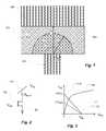
- FIG. 1is a simplified diagram of a mushroom style phase change memory cell including a molten region and a solid region as induced during dynamic resistance measurements described herein.
- FIG. 2is a schematic diagram of a single memory device and access device at a cross point of a bit line and a word line in an array of such devices subjected to testing as described herein
- FIG. 3is a graph of drain to source current versus drain to source voltage for an access device showing dynamic resistance measurements.
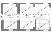
- FIGS. 4 a through 4 fshow the results of measurements of dynamic resistance for six different memory cells fitted to a linear curve.
- FIG. 5is a simplified block diagram of an integrated circuit memory device as described herein including a dynamic resistance test mode.
- FIG. 6is a flowchart of a testing and manufacturing method as described herein.
- FIG. 7has a flowchart of an alternative testing and manufacturing method as described herein.
- FIG. 8is a simplified diagram of a manufacturing line including test station for dynamic resistance tests as described herein.
- FIG. 1is a simplified diagram of a mushroom style phase change memory cell including a bottom electrode 100 , an element 101 comprising a phase change material, and a top electrode 102 .
- the bottom electrode 100 in the illustrated embodimentis a pillar having a radius r 0 at the interface having a contact area, roughly ⁇ r 0 2 , between element 101 and the bottom electrode 100 .
- the top electrode 102contacts the element 101 over substantially greater area than the contact area at the interface between the bottom electrode 100 and element 101 .
- bias circuitry(See, for example, bias circuitry voltage and current sources 555 of FIG. 5 ) applying voltages to an access device coupled to the bottom electrode and a bit line coupled to the top electrode can induce current to flow the memory element 101 .
- bias circuitry(See, for example, bias circuitry voltage and current sources 555 of FIG. 5 ) applying voltages to an access device coupled to the bottom electrode and a bit line coupled to the top electrode can induce current to flow the memory element 101 .
- bias circuitrySee, for example, bias circuitry voltage and current sources 555 of FIG. 5
- applying voltages to an access device coupled to the bottom electrode and a bit line coupled to the top electrodecan induce current to flow the memory element 101 .
- magnitude of current flowis small and insufficient to cause a phase change in the active region of the memory element 101 .
- the current flowis adapted to cause a portion of memory element 101 to increase in temperature above a transition temperature sufficient to induce a phase transition between an amorphous state in active region and a crystalline state in the active
- an active region of the memory element 101occurs adjacent to the interface between the bottom electrode 100 and a memory element 101 .
- a sequence of test pulsesis applied to the memory cell.
- the test pulseshave magnitudes and durations sufficient to cause formation of a molten region 103 within the element 101 , while the remainder of the memory only 101 remains in a solid phase.
- the test pulseshave durations sufficient for thermal transients to dissipate in the element 101 , so that a dynamic resistance measurement can be taken on a relatively stable structure.
- dynamic resistanceis defined as the resistance of the phase change cell when a constant current flows through the cell. This is a steady state measurement.
- Dynamic resistancecan be measured using a simple scheme similar to that used to determine the R-I curve, while ensuring that the access transistor, or other access device, is biased in its linear region. This operation in the linear region enables us to subtract the transistor resistance and obtain the resistance of the phase change element 101 during programming.
- dynamic resistanceis a steady state measurement
- the programming pulsecan be relatively short, such as about 40 ns. All the thermal transients typically settle in less than 5 ns, so the measured resistance is the resistance of the cell when a constant current is flowing through the cell.
- the size of the molten regiondepends on a critical dimension r 0 , and the amount of power (VI) delivered by the test pulse.
- a sequence of test pulses having varying powerssuch as by having varying magnitudes and constant pulse widths, is applied to a memory cell.
- Each test pulsewill induce a roughly hemispherical molten region 103 having a radius x.
- the sequence of test pulsesincludes a subset of test pulses which induce molten regions having a radius between about r 0 , and the thickness H of the element 101 . Because the resistivity ⁇ M of the molten phase change material is significantly different than the resistivity ⁇ S of the solid phase change material, a resistance measurement across the memory element will vary with the radius x.
- FIG. 2illustrates the basic memory cell and access structure implemented within an array, including access transistor 105 having a gate coupled to a word line 106 , a source coupled to ground, and a drain coupled to the memory cell bottom electrode.
- the memory cell top electrodeis coupled to the bit line 107 .
- the resistance R PCE of the phase change element 101 in the memory cellis represented by the resistor symbol in FIG. 2 .
- the sequence of test pulsesis applied to the bit line 107 while the access transistor 105 is used to select a memory cell coupled to the bit line 107 . Current through the memory cell depends on the resistance R PCE of the memory element 101 , as well as the transistor 105 .
- a voltage V WL on the word lineis set to bias the transistor in its linear region after the seen in FIG. 3 .
- FIG. 3is a graph of drain-to-source current I DS versus drain-to-source voltage V DS , including trace 110 for a transistor having a linear region 111 and a saturated region for higher drain voltages.
- Lines 112 and 113are load lines for dynamic resistance measurements where the memory element 101 has a first resistance R PCE and a second resistance R′ PCE , respectively. As can be seen, the current through the memory cell and access structure depends on the resistance of the memory element 101 .
- the bottom and top electrodes 100 and 102may comprise TiAlN or TaAlN, or comprise, for further examples, one or more elements selected from the group consisting of Ti, W, Mo, Al, Ta, Cu, Pt, Ir, La, Ni, N, O and Ru and combinations thereof.
- TiNmay be preferred because it makes a good contact with GST (discussed below) as a memory material, it is a common material used in semiconductor manufacturing, and it provides a good diffusion barrier at the higher temperatures at which GST transitions, typically in the 600-700 degree Celsius range.
- Embodiments of the memory element 101include phase change based memory materials, including chalcogenide based materials and other materials.
- Chalcogensinclude any of the four elements oxygen (O), sulfur (S), selenium (Se), and tellurium (Te), forming part of group VIA of the periodic table.
- Chalcogenidescomprise compounds of a chalcogen with a more electropositive element or radical.
- Chalcogenide alloyscomprise combinations of chalcogenides with other materials such as transition metals.
- a chalcogenide alloyusually contains one or more elements from group IVa of the periodic table of elements, such as germanium (Ge) and tin (Sn).
- chalcogenide alloysinclude combinations including one or more of antimony (Sb), gallium (Ga), indium (In), and silver (Ag).
- Many phase change based memory materialshave been described in technical literature, including alloys of: Ga/Sb, In/Sb, In/Se, Sb/Te, Ge/Te, Ge/Sb/Te, In/Sb/Te, Ga/Se/Te, Sn/Sb/Te, In/Sb/Ge, Ag/In/Sb/Te, Ge/Sn/Sb/Te, Ge/Sb/Se/Te and Te/Ge/Sb/S.
- a wide range of alloy compositionsmay be workable.
- the compositionscan be characterized as Te a Ge b Sb 100 ⁇ (a+b) .
- Chalcogenides and other phase change materialsare doped with impurities in some embodiments to modify conductivity, transition temperature, melting temperature, and other properties of memory elements using the doped chalcogenides.
- Representative impurities used for doping chalcogenidesinclude nitrogen, silicon, oxygen, silicon dioxide, silicon nitride, copper, silver, gold, aluminum, aluminum oxide, tantalum, tantalum oxide, tantalum nitride, titanium and titanium oxide. See, for example U.S. Pat. No. 6,800,504, and U.S. Patent Application Publication No. US 2005/0029502.
- Phase change alloysare capable of being switched between a first structural state in which the material is in a generally amorphous solid phase, and a second structural state in which the material is in a generally crystalline solid phase in its local order in the active channel region of the cell.
- amorphousis used to refer to a relatively less ordered structure, more disordered than a single crystal, which has the detectable characteristics such as higher electrical resistivity than the crystalline phase.
- crystallineis used to refer to a relatively more ordered structure, more ordered than in an amorphous structure, which has detectable characteristics such as lower electrical resistivity than the amorphous phase.
- phase change materialsmay be electrically switched between different detectable states of local order across the spectrum between completely amorphous and completely crystalline states.
- material characteristics affected by the change between amorphous and crystalline phasesinclude atomic order, free electron density and activation energy.
- the materialmay be switched either into different solid phases or into mixtures of two or more solid phases, providing a gray scale between completely amorphous and completely crystalline states.
- the electrical properties in the materialmay vary accordingly.
- test pulses used for measurements described hereincan be determined empirically or by modeling, and specifically adapted to a particular phase change alloy and cell structure.
- a material useful for implementation of a PCRAM described hereinis Ge 2 Sb 2 Te 5 .
- a collimator with an aspect ratio of 1 ⁇ 5can be used to improve the fill-in performance.
- the DC bias of several tens to several hundreds of voltsis also used.
- the combination of DC bias and the collimatorcan be used simultaneously.
- the post deposition annealing treatment with vacuum or N 2 ambientis sometimes needed to improve the crystallize state of chalcogenide material.
- the annealing temperaturetypically ranges 100° C. to 400° C. with an anneal time of less than 30 minutes.
- chalcogenide materialdepends on the design of cell structure.
- a chalcogenide material with thickness of higher than 8 nmcan have a phase change characterization so that the material exhibits at least two stable resistance the states.
- FIGS. 4 a - 4 fare plots of measurements of dynamic resistance in six different memory cells, where the dots are measurements for individual test pulses in a sequence of 40 test pulses about 40 nsec long, which are stepped from 0.6 V to 1.5V in increments of 0.015 V.
- the plotsshow the linear region of the measurements, in which the radius of the molten region is believed to fall in the range between r 0 and H as explained above.
- Table 1 belowshows the results of extraction of the coefficients A and B for 12 selected memory cells.
- the mean value of Ais about 0.5623 and the percent variation of A is about 5%.
- the mean value of Bis about 60.36 and the percent variation of B is about 35%.
- the parameter Adepends only on material properties of the cell, and is independent of cell dimensions in the plotted linear region. Therefore, the percent variation is much smaller than the percent variation in B, which also depends on the dimensions of the cell including r 0 .
- the molten region 103has an electrical resistivity ⁇ M much less than the electrical resistivity ⁇ S of the surrounding solid material in the memory element 101 .
- the resistance of the cellcan be derived from the following equation:
- R⁇ m 4 ⁇ r 0 + ⁇ r 0 x ⁇ ⁇ m ⁇ 1 2 ⁇ ⁇ ⁇ ⁇ y 2 ⁇ d y + ⁇ x H ⁇ ⁇ s ⁇ 1 2 ⁇ ⁇ ⁇ ⁇ y 2 ⁇ d y
- the three components of this computationinclude first, the resistance of the molten hemispherical region having radius r 0 , second the resistance of the molten hemispherical region between radius r 0 and x, and the resistance of the solid material between x and H.
- the radius xis proportional to the amount of energy applied during the test pulse.
- the slope Adepends only on the material properties k 1 , ⁇ S and ⁇ M .
- the intercept Bdepends on material properties plus critical dimensions of the memory element r 0 and H.
- the slope Ais related to material properties of the memory cell being tested
- the intercept Bis related to the material properties and to the physical structure of the cell.
- a healthy cellshould have stable A and B values.
- a stable manufacturing lineshould have stable A and B values between the cells within the array, between die, between wafers and between lots.
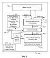
- FIG. 5is a simplified block diagram of an integrated circuit in accordance with an embodiment.
- the integrated circuit 500includes a memory array 505 implemented using phase change memory cells as described.
- a row decoder 510 having read, set and reset modesis coupled to a plurality of word lines 515 arranged along rows in the memory array 505 .
- Block 505 arepresents probe points on the array suitable for coupling to a testing machine for the measurement of dynamic resistance. Alternatively, circuitry may be provided on chip to provide output indicating such measurements.
- a column decoder 520is coupled to a plurality of bit lines 525 arranged along columns in the memory array 505 for reading, setting and resetting memory cells in the memory array 505 .
- Addressesare supplied on bus 560 to column decoder 520 and row decoder 510 .
- Sense amplifiers and data-in structures in block 530are coupled to the column decoder 520 via data bus 535 .
- Datais supplied via the data-in line 540 from input/output ports on the integrated circuit 500 or from other data sources internal or external to the integrated circuit 500 , to the data-in structures in block 530 .
- other circuitry 565is included on the integrated circuit 500 , such as a general purpose processor or special purpose application circuitry, or a combination of modules providing system-on-a-chip functionality supported by the phase change memory cell array.
- Datais supplied via the data-out line 545 from the sense amplifiers in block 530 to input/output ports on the integrated circuit 500 , or to other data destinations internal or external to the integrated circuit 500 .
- a controller implemented in this example using bias arrangement state machine 550controls the bias circuitry voltage and current sources 555 for the application of bias arrangements including read, set, reset and verify voltages and or currents for the word lines and bit lines, and controls the word line/source line operation using an access control process.
- the state machine 550may include out logic supporting a process for measuring dynamic resistance as described herein, including the generation of sequences of test pulses in coordination with the bias circuitry voltage and current sources 555 , and other supporting logic functions, including parameter registers for storing the parameter sets in a machine-readable format extracted, as necessary.
- the controllercan be implemented using special-purpose logic circuitry as known in the art.
- the controllercomprises a general-purpose processor, which may be implemented on the same integrated circuit, which executes a computer program to control the operations of the device.
- a combination of special-purpose logic circuitry and a general-purpose processormay be utilized for implementation of the controller.
- Another embodimentconsists of a similar integrated circuit as shown in FIG. 5 but without block 505 a .
- the dynamic resistance measurementsare performed by a special test mode through the integrated circuit.
- a separated test structure to the main memory arrayis provided for the dynamic resistance measurement.
- This test structurecan have the similar cell design as the memory array 505 in the integrated circuit 500 , or can have special design for testing purpose.
- FIG. 6is a flow chart for a manufacturing and testing process according to the present invention. As illustrated, the process begins with performing manufacturing processes sufficient to produce a testable cell on a memory device (block 601 ). The device is coupled to a testing machine, and probes are applied the probe points on the device to which a sequence of test pulses is applied (block 602 ). The dynamic resistance is measured during the test pulses (block 603 ). A parameter set is extracted including the slope A and intercept B as explained above for a linear fitting equation (block 604 ). The parameter set is then associated with the memory device, by storing it in a machine-readable format in a register file on the chip, or in memory on the test workstation associated with the tested chip (block 605 ).
- a manufacturing stepis performed in response to the parameter set (block 606 ).
- Representative manufacturing stepsinclude, if the parameter set falls outside the specified range, discarding the memory device, or stopping the manufacturing of further devices pending analysis of the manufacturing line and reasons for the detected anomalies, and so on.
- FIG. 7is a flow chart of an alternative manufacturing and testing process which measures changes in the parameter set after applying a stress to the memory device.
- the processbegins with performing manufacturing processes sufficient to produce a testable cell on a memory device (block 701 ).
- the deviceis coupled to a testing machine, and probes are applied these probe points on the device to which a sequence of test pulses is applied (block 702 ).
- the dynamic resistanceis measured during the test pulses (block 703 ).
- a first parameter setis extracted including the slope A and intercept B as explained above for a linear fitting equation (block 704 ).
- the first parameter setis then associated with the memory device, by storing in a machine-readable format and a register file on the chip, or in memory on the test workstation (block 705 ).
- a stressis applied to the memory cell, such as reset/set cycling, a long pulse, or the like (block 706 ).
- a second sequence of test pulsesis applied to the memory cell (block 707 ).
- the dynamic resistanceis measured during the second sequence of test pulses (block 708 ).
- a second parameter setis extracted including the slope A and intercept B as explained above for a linear fitting equation (block 709 ).
- the second parameter setis then associated with the memory device, by storing in a machine-readable format in a register file on the chip, or in memory on the test workstation (block 710 ).
- a manufacturing stepis performed in response to the analysis of the first and second parameter sets (block 711 ). Representative manufacturing steps include, if the change in the parameter sets falls outside the specified range, discarding the memory device, or stopping the manufacturing of further devices pending analysis of the manufacturing line and reasons for the detected anomalies, and so on.
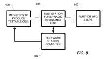
- FIG. 8is a simplified block diagram of the manufacturing line including equipment for performing the dynamic resistance test as described above.
- Such manufacturing lineincludes fabrication equipment 800 for performing manufacturing steps to produce a testable cell on a wafer.
- the wafer including the testable cellis moved to test station 801 , in which the device is probed as explained above for measuring the dynamic resistance.
- the test stationis coupled to a test workstation 802 which gathers the parameter sets as explained above, and performs such data processing has necessary to produce commands that affect a manufacturing operations.
- the memory deviceis passed to equipment 803 for further manufacturing steps, such as dicing the wafer containing the device, packaging the device and so on.
Landscapes
- Semiconductor Memories (AREA)
Abstract
Description
| TABLE 1 | |||
| A | B | ||
| 0.60287 | 26.049 | ||
| 0.54801 | 80.396 | ||
| 0.54859 | 59.396 | ||
| 0.50238 | 110.56 | ||
| 0.54205 | 55.382 | ||
| 0.53921 | 75.798 | ||
| 0.56577 | 48.71 | ||
| 0.58452 | 62.407 | ||
| 0.58018 | 40.884 | ||
| 0.55871 | 56.958 | ||
| 0.58769 | 53.065 | ||
| 0.5879 | 54.8 | ||
x=k1I
Claims (21)
R=A/I+B,
R=A/I+B,
Priority Applications (3)
| Application Number | Priority Date | Filing Date | Title |
|---|---|---|---|
| US11/970,348US7639527B2 (en) | 2008-01-07 | 2008-01-07 | Phase change memory dynamic resistance test and manufacturing methods |
| TW097103164ATWI365293B (en) | 2008-01-07 | 2008-01-28 | Phase change memory dynamic resistance test and manufacturing methods |
| CN200910001340.5ACN101562050B (en) | 2008-01-07 | 2009-01-07 | A kind of testing and manufacturing method of phase change memory |
Applications Claiming Priority (1)
| Application Number | Priority Date | Filing Date | Title |
|---|---|---|---|
| US11/970,348US7639527B2 (en) | 2008-01-07 | 2008-01-07 | Phase change memory dynamic resistance test and manufacturing methods |
Publications (2)
| Publication Number | Publication Date |
|---|---|
| US20090175071A1 US20090175071A1 (en) | 2009-07-09 |
| US7639527B2true US7639527B2 (en) | 2009-12-29 |
Family
ID=40844416
Family Applications (1)
| Application Number | Title | Priority Date | Filing Date |
|---|---|---|---|
| US11/970,348Expired - Fee RelatedUS7639527B2 (en) | 2008-01-07 | 2008-01-07 | Phase change memory dynamic resistance test and manufacturing methods |
Country Status (3)
| Country | Link |
|---|---|
| US (1) | US7639527B2 (en) |
| CN (1) | CN101562050B (en) |
| TW (1) | TWI365293B (en) |
Cited By (3)
| Publication number | Priority date | Publication date | Assignee | Title |
|---|---|---|---|---|
| US20100165717A1 (en)* | 2008-12-26 | 2010-07-01 | Joo-Ae Lee | Write driver circuit of pram |
| US20130016556A1 (en)* | 2010-06-25 | 2013-01-17 | International Business Machines Corporation | Planar phase- change memory cell with parallel electrical paths |
| US9196829B2 (en) | 2010-08-31 | 2015-11-24 | Globalfoundries Inc. | Post-fabrication self-aligned initialization of integrated devices |
Families Citing this family (8)
| Publication number | Priority date | Publication date | Assignee | Title |
|---|---|---|---|---|
| CN101777388B (en)* | 2010-01-08 | 2012-08-08 | 中国科学院上海微系统与信息技术研究所 | Method for obtaining phase-change memory phase-change resistance crystallization rate |
| CN102354537B (en)* | 2011-07-06 | 2014-03-05 | 华中科技大学 | A kind of testing method of phase-change memory chip |
| US8787065B2 (en) | 2011-10-18 | 2014-07-22 | Micron Technology, Inc. | Apparatuses and methods for determining stability of a memory cell |
| CN106558347B (en)* | 2015-09-25 | 2020-06-09 | 中芯国际集成电路制造(上海)有限公司 | Programming test method of phase change memory |
| CN106824833B (en)* | 2017-02-28 | 2023-07-18 | 中国振华集团云科电子有限公司 | Resistor screening process |
| CN108648782B (en)* | 2018-04-23 | 2020-11-13 | 中国科学院上海微系统与信息技术研究所 | A Screening Method for Optimal Pulse Operating Conditions of Phase Change Memory |
| CN111383705A (en)* | 2018-12-30 | 2020-07-07 | 中电海康集团有限公司 | Test circuit and test method of memory |
| US11475950B2 (en)* | 2020-04-01 | 2022-10-18 | Taiwan Semiconductor Manufacturing Co., Ltd. | Stressing algorithm for solving cell-to-cell variations in phase change memory |
Citations (197)
| Publication number | Priority date | Publication date | Assignee | Title |
|---|---|---|---|---|
| US3271591A (en) | 1963-09-20 | 1966-09-06 | Energy Conversion Devices Inc | Symmetrical current controlling device |
| US3530441A (en) | 1969-01-15 | 1970-09-22 | Energy Conversion Devices Inc | Method and apparatus for storing and retrieving information |
| US4599705A (en) | 1979-12-13 | 1986-07-08 | Energy Conversion Devices, Inc. | Programmable cell for use in programmable electronic arrays |
| US4719594A (en) | 1984-11-01 | 1988-01-12 | Energy Conversion Devices, Inc. | Grooved optical data storage device including a chalcogenide memory layer |
| US4876220A (en) | 1986-05-16 | 1989-10-24 | Actel Corporation | Method of making programmable low impedance interconnect diode element |
| US4959812A (en) | 1987-12-28 | 1990-09-25 | Kabushiki Kaisha Toshiba | Electrically erasable programmable read-only memory with NAND cell structure |
| US5106775A (en) | 1987-12-10 | 1992-04-21 | Hitachi, Ltd. | Process for manufacturing vertical dynamic random access memories |
| US5166096A (en) | 1991-10-29 | 1992-11-24 | International Business Machines Corporation | Process for fabricating self-aligned contact studs for semiconductor structures |
| US5166758A (en) | 1991-01-18 | 1992-11-24 | Energy Conversion Devices, Inc. | Electrically erasable phase change memory |
| US5177567A (en) | 1991-07-19 | 1993-01-05 | Energy Conversion Devices, Inc. | Thin-film structure for chalcogenide electrical switching devices and process therefor |
| US5332923A (en) | 1991-08-06 | 1994-07-26 | Nec Corporation | Semiconductor memory |
| US5391901A (en) | 1992-10-30 | 1995-02-21 | Nec Corporation | Semiconductor memory with oblique folded bit-line arrangement |
| US5534712A (en) | 1991-01-18 | 1996-07-09 | Energy Conversion Devices, Inc. | Electrically erasable memory elements characterized by reduced current and improved thermal stability |
| US5550396A (en) | 1992-01-24 | 1996-08-27 | Mitsubishi Denki Kabushiki Kaisha | Vertical field effect transistor with a trench structure |
| US5687112A (en) | 1996-04-19 | 1997-11-11 | Energy Conversion Devices, Inc. | Multibit single cell memory element having tapered contact |
| US5789758A (en) | 1995-06-07 | 1998-08-04 | Micron Technology, Inc. | Chalcogenide memory cell with a plurality of chalcogenide electrodes |
| US5789277A (en) | 1996-07-22 | 1998-08-04 | Micron Technology, Inc. | Method of making chalogenide memory device |
| US5814527A (en) | 1996-07-22 | 1998-09-29 | Micron Technology, Inc. | Method of making small pores defined by a disposable internal spacer for use in chalcogenide memories |
| US5831276A (en) | 1995-06-07 | 1998-11-03 | Micron Technology, Inc. | Three-dimensional container diode for use with multi-state material in a non-volatile memory cell |
| US5837564A (en) | 1995-11-01 | 1998-11-17 | Micron Technology, Inc. | Method for optimal crystallization to obtain high electrical performance from chalcogenides |
| US5869843A (en) | 1995-06-07 | 1999-02-09 | Micron Technology, Inc. | Memory array having a multi-state element and method for forming such array or cells thereof |
| US5879955A (en) | 1995-06-07 | 1999-03-09 | Micron Technology, Inc. | Method for fabricating an array of ultra-small pores for chalcogenide memory cells |
| US5902704A (en) | 1997-07-02 | 1999-05-11 | Lsi Logic Corporation | Process for forming photoresist mask over integrated circuit structures with critical dimension control |
| US5933365A (en) | 1997-06-19 | 1999-08-03 | Energy Conversion Devices, Inc. | Memory element with energy control mechanism |
| US5952671A (en) | 1997-05-09 | 1999-09-14 | Micron Technology, Inc. | Small electrode for a chalcogenide switching device and method for fabricating same |
| US5958358A (en) | 1992-07-08 | 1999-09-28 | Yeda Research And Development Co., Ltd. | Oriented polycrystalline thin films of transition metal chalcogenides |
| US5970336A (en) | 1996-08-22 | 1999-10-19 | Micron Technology, Inc. | Method of making memory cell incorporating a chalcogenide element |
| US5985698A (en) | 1996-07-22 | 1999-11-16 | Micron Technology, Inc. | Fabrication of three dimensional container diode for use with multi-state material in a non-volatile memory cell |
| US6011725A (en) | 1997-08-01 | 2000-01-04 | Saifun Semiconductors, Ltd. | Two bit non-volatile electrically erasable and programmable semiconductor memory cell utilizing asymmetrical charge trapping |
| US6025220A (en) | 1996-06-18 | 2000-02-15 | Micron Technology, Inc. | Method of forming a polysilicon diode and devices incorporating such diode |
| US6031287A (en) | 1997-06-18 | 2000-02-29 | Micron Technology, Inc. | Contact structure and memory element incorporating the same |
| US6034882A (en) | 1998-11-16 | 2000-03-07 | Matrix Semiconductor, Inc. | Vertically stacked field programmable nonvolatile memory and method of fabrication |
| US6066870A (en) | 1996-07-16 | 2000-05-23 | Micron Technology, Inc. | Single digit line with cell contact interconnect |
| US6087269A (en) | 1998-04-20 | 2000-07-11 | Advanced Micro Devices, Inc. | Method of making an interconnect using a tungsten hard mask |
| US6087674A (en) | 1996-10-28 | 2000-07-11 | Energy Conversion Devices, Inc. | Memory element with memory material comprising phase-change material and dielectric material |
| US6114713A (en) | 1997-01-28 | 2000-09-05 | Zahorik; Russell C. | Integrated circuit memory cell having a small active area and method of forming same |
| US6117720A (en) | 1995-06-07 | 2000-09-12 | Micron Technology, Inc. | Method of making an integrated circuit electrode having a reduced contact area |
| US6147395A (en) | 1996-10-02 | 2000-11-14 | Micron Technology, Inc. | Method for fabricating a small area of contact between electrodes |
| WO2000079539A1 (en) | 1999-06-22 | 2000-12-28 | Ovonyx, Inc. | Method of programming phase-change memory element |
| US6177317B1 (en) | 1999-04-14 | 2001-01-23 | Macronix International Co., Ltd. | Method of making nonvolatile memory devices having reduced resistance diffusion regions |
| WO2001045108A1 (en) | 1999-12-16 | 2001-06-21 | Ovonyx, Inc. | Programmable resistance memory arrays with reference cells |
| US6271090B1 (en) | 2000-12-22 | 2001-08-07 | Macronix International Co., Ltd. | Method for manufacturing flash memory device with dual floating gates and two bits per cell |
| US6280684B1 (en) | 1994-12-13 | 2001-08-28 | Ricoh Company, Ltd. | Sputtering target, method of producing the target, optical recording medium fabricated by using the sputtering target, and method of fabricating the optical recording medium |
| US6316348B1 (en) | 1999-02-05 | 2001-11-13 | Taiwan Semiconductor Manufacturing Company | High selectivity Si-rich SiON etch-stop layer |
| US6320786B1 (en) | 2000-12-22 | 2001-11-20 | Macronix International Co., Ltd. | Method of controlling multi-state NROM |
| US20010055838A1 (en) | 2000-04-28 | 2001-12-27 | Matrix Semiconductor Inc. | Nonvolatile memory on SOI and compound semiconductor substrates and method of fabrication |
| US6339544B1 (en) | 2000-09-29 | 2002-01-15 | Intel Corporation | Method to enhance performance of thermal resistor device |
| US6351406B1 (en) | 1998-11-16 | 2002-02-26 | Matrix Semiconductor, Inc. | Vertically stacked field programmable nonvolatile memory and method of fabrication |
| US6372651B1 (en) | 1998-07-17 | 2002-04-16 | Advanced Micro Devices, Inc. | Method for trimming a photoresist pattern line for memory gate etching |
| US6380068B2 (en) | 2000-01-05 | 2002-04-30 | Macronix International Co., Ltd. | Method for planarizing a flash memory device |
| US20020072223A1 (en) | 1999-12-22 | 2002-06-13 | Gilbert Stephen R. | Method of enhancing adhesion of a conductive barrier layer to an underlying conductive plug and contact for ferroelectric applications |
| US20020070457A1 (en) | 2000-12-09 | 2002-06-13 | Samsung Electronics Co., Ltd. | Metal contact structure in semiconductor device and method for forming the same |
| US20020081833A1 (en) | 2000-12-22 | 2002-06-27 | Li Calvin K. | Patterning three dimensional structures |
| US6420216B1 (en) | 2000-03-14 | 2002-07-16 | International Business Machines Corporation | Fuse processing using dielectric planarization pillars |
| US6420215B1 (en) | 2000-04-28 | 2002-07-16 | Matrix Semiconductor, Inc. | Three-dimensional memory array and method of fabrication |
| US6429064B1 (en) | 2000-09-29 | 2002-08-06 | Intel Corporation | Reduced contact area of sidewall conductor |
| US20020113273A1 (en) | 2001-02-22 | 2002-08-22 | Samsung Electronics Co., Ltd. | Semiconductor device having contact plug and method for manufacturing the same |
| US6440837B1 (en) | 2000-07-14 | 2002-08-27 | Micron Technology, Inc. | Method of forming a contact structure in a semiconductor device |
| US6483736B2 (en) | 1998-11-16 | 2002-11-19 | Matrix Semiconductor, Inc. | Vertically stacked field programmable nonvolatile memory and method of fabrication |
| US6487114B2 (en) | 2001-02-28 | 2002-11-26 | Macronix International Co., Ltd. | Method of reading two-bit memories of NROM cell |
| US20020182835A1 (en) | 2001-05-29 | 2002-12-05 | Quinn Robert M. | Method for manufacturing contacts for a Chalcogenide memory device |
| US6501111B1 (en) | 2000-06-30 | 2002-12-31 | Intel Corporation | Three-dimensional (3D) programmable device |
| US6512241B1 (en) | 2001-12-31 | 2003-01-28 | Intel Corporation | Phase change material memory device |
| US6511867B2 (en) | 2001-06-30 | 2003-01-28 | Ovonyx, Inc. | Utilizing atomic layer deposition for programmable device |
| US6514820B2 (en) | 1998-08-27 | 2003-02-04 | Micron Technology, Inc. | Method for forming single electron resistor memory |
| US6534781B2 (en) | 2000-12-26 | 2003-03-18 | Ovonyx, Inc. | Phase-change memory bipolar array utilizing a single shallow trench isolation for creating an individual active area region for two memory array elements and one bipolar base contact |
| US6545903B1 (en) | 2001-12-17 | 2003-04-08 | Texas Instruments Incorporated | Self-aligned resistive plugs for forming memory cell with phase change material |
| US6551866B1 (en) | 1998-11-27 | 2003-04-22 | Mitsubishi Denki Kabushiki Kaisha | Method of manufacturing a semiconductor memory device |
| US6555860B2 (en) | 2000-09-29 | 2003-04-29 | Intel Corporation | Compositionally modified resistive electrode |
| US6563156B2 (en) | 2001-03-15 | 2003-05-13 | Micron Technology, Inc. | Memory elements and methods for making same |
| US6566700B2 (en) | 2001-10-11 | 2003-05-20 | Ovonyx, Inc. | Carbon-containing interfacial layer for phase-change memory |
| US6567293B1 (en) | 2000-09-29 | 2003-05-20 | Ovonyx, Inc. | Single level metal memory cell using chalcogenide cladding |
| US20030095426A1 (en) | 2001-11-20 | 2003-05-22 | Glen Hush | Complementary bit PCRAM sense amplifier and method of operation |
| US6579760B1 (en) | 2002-03-28 | 2003-06-17 | Macronix International Co., Ltd. | Self-aligned, programmable phase change memory |
| US6584589B1 (en)* | 2000-02-04 | 2003-06-24 | Hewlett-Packard Development Company, L.P. | Self-testing of magneto-resistive memory arrays |
| US6586761B2 (en) | 2001-09-07 | 2003-07-01 | Intel Corporation | Phase change material memory device |
| US6589714B2 (en) | 2001-06-26 | 2003-07-08 | Ovonyx, Inc. | Method for making programmable resistance memory element using silylated photoresist |
| US6605821B1 (en) | 2002-05-10 | 2003-08-12 | Hewlett-Packard Development Company, L.P. | Phase change material electronic memory structure and method for forming |
| US6605527B2 (en) | 2001-06-30 | 2003-08-12 | Intel Corporation | Reduced area intersection between electrode and programming element |
| US6613604B2 (en) | 2001-08-02 | 2003-09-02 | Ovonyx, Inc. | Method for making small pore for use in programmable resistance memory element |
| US6617192B1 (en) | 1997-10-01 | 2003-09-09 | Ovonyx, Inc. | Electrically programmable memory element with multi-regioned contact |
| US6620715B1 (en) | 2002-03-29 | 2003-09-16 | Cypress Semiconductor Corp. | Method for forming sub-critical dimension structures in an integrated circuit |
| US6639849B2 (en) | 2002-02-28 | 2003-10-28 | Fujitsu Limited | Nonvolatile semiconductor memory device programming second dynamic reference cell according to threshold value of first dynamic reference cell |
| CN1462478A (en) | 2000-09-22 | 2003-12-17 | 三因迪斯克公司 | Non-volatile memory cell array and method of forming |
| US6673700B2 (en) | 2001-06-30 | 2004-01-06 | Ovonyx, Inc. | Reduced area intersection between electrode and programming element |
| US6674115B2 (en) | 2001-08-31 | 2004-01-06 | Intel Corporation | Multiple layer phrase-change memory |
| US20040026686A1 (en) | 2002-08-09 | 2004-02-12 | Macronix International Co., Ltd. | Spacer chalcogenide memory method and device |
| US20040051161A1 (en) | 2002-04-09 | 2004-03-18 | Matsushita Electric Industrial Co., Ltd. | Non-volatile memory and the fabrication method thereof |
| US20040051094A1 (en) | 2002-09-13 | 2004-03-18 | Mitsubishi Denki Kabushiki Kaisha | Non-volatile semiconductor memory device allowing shrinking of memory cell |
| US6744088B1 (en) | 2002-12-13 | 2004-06-01 | Intel Corporation | Phase change memory device on a planar composite layer |
| US6746892B2 (en) | 2002-04-04 | 2004-06-08 | Hewlett-Packard Development Company, L.P. | Low heat loss and small contact area composite electrode for a phase change media memory device |
| US6750079B2 (en) | 1999-03-25 | 2004-06-15 | Ovonyx, Inc. | Method for making programmable resistance memory element |
| US20040113232A1 (en) | 2002-12-13 | 2004-06-17 | Johnson Brian G. | Phase change memory |
| US20040165422A1 (en) | 2003-02-24 | 2004-08-26 | Horii Hideki | Phase changeable memory devices and methods for fabricating the same |
| US20040178172A1 (en) | 2003-03-11 | 2004-09-16 | Taiwan Semiconductor Manufacturing Co., Ltd. | Method of removing metal etching residues following a metal etchback process to improve a CMP process |
| US6797979B2 (en) | 2000-12-21 | 2004-09-28 | Intel Corporation | Metal structure for a phase-change memory device |
| US6800504B2 (en) | 2001-08-30 | 2004-10-05 | Micron Technology, Inc. | Integrated circuit device and fabrication using metal-doped chalcogenide materials |
| US6805563B2 (en) | 2002-09-10 | 2004-10-19 | Enplas Corporation | Socket for electrical parts |
| US20040208038A1 (en) | 2002-10-31 | 2004-10-21 | Dai Nippon Prtg. Co., Ltd. | Phase change-type memory element and process for producing the same |
| US6808991B1 (en) | 2003-11-19 | 2004-10-26 | Macronix International Co., Ltd. | Method for forming twin bit cell flash memory |
| US6815704B1 (en) | 2003-09-04 | 2004-11-09 | Silicon Storage Technology, Inc. | Phase change memory device employing thermally insulating voids |
| US20050019975A1 (en) | 2003-07-23 | 2005-01-27 | Se-Ho Lee | Phase change memory devices having phase change area in porous dielectric layer and methods for manufacturing the same |
| US20050018526A1 (en) | 2003-07-21 | 2005-01-27 | Heon Lee | Phase-change memory device and manufacturing method thereof |
| US6850432B2 (en) | 2002-08-20 | 2005-02-01 | Macronix International Co., Ltd. | Laser programmable electrically readable phase-change memory method and device |
| US20050029502A1 (en) | 2003-08-04 | 2005-02-10 | Hudgens Stephen J. | Processing phase change material to improve programming speed |
| US6861267B2 (en) | 2001-09-17 | 2005-03-01 | Intel Corporation | Reducing shunts in memories with phase-change material |
| US6864500B2 (en) | 2002-04-10 | 2005-03-08 | Micron Technology, Inc. | Programmable conductor memory cell structure |
| US6867638B2 (en) | 2002-01-10 | 2005-03-15 | Silicon Storage Technology, Inc. | High voltage generation and regulation system for digital multilevel nonvolatile memory |
| US20050062087A1 (en) | 2003-09-19 | 2005-03-24 | Yi-Chou Chen | Chalcogenide phase-change non-volatile memory, memory device and method for fabricating the same |
| US6894305B2 (en) | 2003-02-24 | 2005-05-17 | Samsung Electronics Co., Ltd. | Phase-change memory devices with a self-heater structure |
| US6894304B2 (en) | 2001-08-27 | 2005-05-17 | Micron Technology, Inc. | Apparatus and method for dual cell common electrode PCRAM memory device |
| US20050106919A1 (en) | 2003-11-18 | 2005-05-19 | Agere Systems Inc. | Contact for use in an integrated circuit and a method of manufacture therefor |
| US6903362B2 (en) | 2001-05-09 | 2005-06-07 | Science Applications International Corporation | Phase change switches and circuits coupling to electromagnetic waves containing phase change switches |
| US20050130414A1 (en) | 2003-12-12 | 2005-06-16 | Suk-Hun Choi | Methods for forming small features in microelectronic devices using sacrificial layers and structures fabricated by same |
| US6909107B2 (en) | 2002-12-30 | 2005-06-21 | Bae Systems, Information And Electronic Systems Integration, Inc. | Method for manufacturing sidewall contacts for a chalcogenide memory device |
| US20050167656A1 (en) | 2004-01-30 | 2005-08-04 | International Business Machines Corporation | Phase-change memory cell and method of fabricating the phase-change memory cell |
| US6927410B2 (en) | 2003-09-04 | 2005-08-09 | Silicon Storage Technology, Inc. | Memory device with discrete layers of phase change memory material |
| US6933516B2 (en) | 2001-10-11 | 2005-08-23 | Ovonyx, Inc. | Forming tapered lower electrode phase-change memories |
| US6937507B2 (en) | 2003-12-05 | 2005-08-30 | Silicon Storage Technology, Inc. | Memory device and method of operating same |
| US20050191804A1 (en) | 2004-03-01 | 2005-09-01 | Taiwan Semiconductor Manufacturing Co., Ltd. | Method for forming a reduced active area in a phase change memory structure |
| US6943365B2 (en) | 1999-03-25 | 2005-09-13 | Ovonyx, Inc. | Electrically programmable memory element with reduced area of contact and method for making same |
| US20050201182A1 (en) | 2004-03-12 | 2005-09-15 | Kenichi Osada | Semiconductor device |
| US20050215009A1 (en) | 2004-03-19 | 2005-09-29 | Sung-Lae Cho | Methods of forming phase-change memory devices |
| US20050212024A1 (en) | 2004-03-24 | 2005-09-29 | Infineon Technologies Ag | Memory device with an active material embedded in an insulating material |
| US6969866B1 (en) | 1997-10-01 | 2005-11-29 | Ovonyx, Inc. | Electrically programmable memory element with improved contacts |
| US6972428B2 (en) | 2001-06-26 | 2005-12-06 | Ovonyx, Inc. | Programmable resistance memory element |
| US6972430B2 (en) | 2002-02-20 | 2005-12-06 | Stmicroelectronics S.R.L. | Sublithographic contact structure, phase change memory cell with optimized heater shape, and manufacturing method thereof |
| US20050285096A1 (en) | 2000-02-11 | 2005-12-29 | Axon Technologies Corporation | Programmable structure, an array including the structure, and methods of forming the same |
| US6992932B2 (en) | 2002-10-29 | 2006-01-31 | Saifun Semiconductors Ltd | Method circuit and system for read error detection in a non-volatile memory array |
| US20060038221A1 (en) | 2004-08-21 | 2006-02-23 | Samsung Electronics Co., Ltd. | Antiferromagnetic/paramagnetic resistive device, non-volatile memory and method for fabricating the same |
| US20060043617A1 (en) | 2004-08-30 | 2006-03-02 | Abbott Todd R | DRAM layout with vertical FETs and method of formation |
| US7023009B2 (en) | 1997-10-01 | 2006-04-04 | Ovonyx, Inc. | Electrically programmable memory element with improved contacts |
| US20060073642A1 (en) | 2003-07-21 | 2006-04-06 | Macronix International Co., Ltd. | Method for manufacturing a multiple-bit-per-cell memory |
| US20060091476A1 (en) | 2004-10-29 | 2006-05-04 | Cay-Uwe Pinnow | Sub-lithographic structures, devices including such structures, and methods for producing the same |
| US7042001B2 (en) | 2004-01-29 | 2006-05-09 | Samsung Electronics Co., Ltd. | Phase change memory devices including memory elements having variable cross-sectional areas |
| US20060110888A1 (en) | 2004-10-19 | 2006-05-25 | Byeong-Ok Cho | Phase changeable memory device and method of formation thereof |
| US20060110878A1 (en) | 2004-11-22 | 2006-05-25 | Macronix International Co., Ltd. | Side wall active pin memory and manufacturing method |
| US20060118913A1 (en) | 2004-12-06 | 2006-06-08 | Samsung Electronics Co., Ltd. | Phase changeable memory cells and methods of forming the same |
| US7067864B2 (en) | 2001-01-30 | 2006-06-27 | Renesas Technology Corp. | SRAM having an improved capacitor |
| US7067865B2 (en) | 2003-06-06 | 2006-06-27 | Macronix International Co., Ltd. | High density chalcogenide memory cells |
| US20060154185A1 (en) | 2005-01-11 | 2006-07-13 | Taiwan Semiconductor Manufacturing Co., Ltd. | Method for forming a finely patterned resist |
| US20060175599A1 (en) | 2005-02-10 | 2006-08-10 | Infineon Technologies North America Corp. | Phase change memory cell with high read margin at low power operation |
| US20060226409A1 (en) | 2005-04-06 | 2006-10-12 | International Business Machines Corporation | Structure for confining the switching current in phase memory (PCM) cells |
| US7122824B2 (en) | 2003-01-15 | 2006-10-17 | Stmicroelectronics S.R.L. | Sublithographic contact structure, in particular for a phase change memory cell, and fabrication process thereof |
| US7122281B2 (en) | 2002-02-26 | 2006-10-17 | Synopsys, Inc. | Critical dimension control using full phase and trim masks |
| US20060234138A1 (en) | 2003-09-30 | 2006-10-19 | Rodger Fehlhaber | Hard mask arrangement |
| US7126149B2 (en) | 2004-01-21 | 2006-10-24 | Renesas Technology Corp. | Phase change memory and phase change recording medium |
| US20060281216A1 (en) | 2005-06-10 | 2006-12-14 | Heon Yong Chang | Method of manufacturing a phase change RAM device utilizing reduced phase change current |
| US20060284279A1 (en) | 2005-06-17 | 2006-12-21 | Macronix International Co., Ltd. | Thin film fuse phase change RAM and manufacturing method |
| US20060286743A1 (en) | 2005-06-17 | 2006-12-21 | Macronix International Co., Ltd. | Method for Manufacturing a Narrow Structure on an Integrated Circuit |
| US20060284214A1 (en) | 2005-06-17 | 2006-12-21 | Macronix International Co., Ltd. | Thin film fuse phase change cell with thermal isolation layer and manufacturing method |
| US20060284157A1 (en) | 2005-06-17 | 2006-12-21 | Macronix International Co., Ltd. | Thin film plate phase change RAM circuit and manufacturing method |
| US20060284158A1 (en) | 2005-06-17 | 2006-12-21 | Macronix International Co., Ltd. | Self-aligned, embedded phase change ram and manufacturing method |
| US20060286709A1 (en) | 2005-06-17 | 2006-12-21 | Macronix International Co., Ltd. | Manufacturing methods for thin film fuse phase change ram |
| US20070010054A1 (en) | 2005-07-08 | 2007-01-11 | Nanochip, Inc. | Method for forming patterned media for a high density data storage device |
| US7164147B2 (en) | 2003-05-23 | 2007-01-16 | Samsung Electronics Co., Ltd. | Semiconductor memory device and method of fabricating the same |
| US7166533B2 (en) | 2005-04-08 | 2007-01-23 | Infineon Technologies, Ag | Phase change memory cell defined by a pattern shrink material process |
| US20070030721A1 (en) | 2001-07-25 | 2007-02-08 | Nantero, Inc. | Device selection circuitry constructed with nanotube technology |
| US20070037101A1 (en) | 2005-08-15 | 2007-02-15 | Fujitsu Limited | Manufacture method for micro structure |
| US20070096162A1 (en) | 2005-11-02 | 2007-05-03 | Thomas Happ | Phase change memory having multilayer thermal insulation |
| US20070108429A1 (en) | 2005-11-14 | 2007-05-17 | Macronix International Co., Ltd. | Pipe shaped phase change memory |
| US20070109843A1 (en) | 2005-11-15 | 2007-05-17 | Macronix International Co., Ltd. | Phase Change Memory Device and Manufacturing Method |
| US20070108430A1 (en) | 2005-11-15 | 2007-05-17 | Macronix International Co., Ltd. | Thermally contained/insulated phase change memory device and method (combined) |
| US20070111429A1 (en) | 2005-11-14 | 2007-05-17 | Macronix International Co., Ltd. | Method of manufacturing a pipe shaped phase change memory |
| US20070108431A1 (en) | 2005-11-15 | 2007-05-17 | Chen Shih H | I-shaped phase change memory cell |
| US20070108077A1 (en) | 2005-11-16 | 2007-05-17 | Macronix International Co., Ltd. | Spacer Electrode Small Pin Phase Change Memory RAM and Manufacturing Method |
| US7220983B2 (en) | 2004-12-09 | 2007-05-22 | Macronix International Co., Ltd. | Self-aligned small contact phase-change memory method and device |
| US20070115794A1 (en) | 2005-11-21 | 2007-05-24 | Macronix International Co., Ltd. | Thermal isolation for an active-sidewall phase change memory cell |
| US20070117315A1 (en) | 2005-11-22 | 2007-05-24 | Macronix International Co., Ltd. | Memory cell device and manufacturing method |
| US20070121374A1 (en) | 2005-11-15 | 2007-05-31 | Macronix International Co., Ltd. | Phase Change Memory Device and Manufacturing Method |
| US20070121363A1 (en) | 2005-11-28 | 2007-05-31 | Macronix International Co., Ltd. | Phase Change Memory Cell and Manufacturing Method |
| US20070126040A1 (en) | 2005-11-21 | 2007-06-07 | Hsiang-Lan Lung | Vacuum cell thermal isolation for a phase change memory device |
| US20070131980A1 (en) | 2005-11-21 | 2007-06-14 | Lung Hsiang L | Vacuum jacket for phase change memory element |
| US20070131922A1 (en) | 2005-12-13 | 2007-06-14 | Macronix International Co., Ltd. | Thin Film Fuse Phase Change Cell with Thermal Isolation Pad and Manufacturing Method |
| US20070138458A1 (en) | 2005-06-17 | 2007-06-21 | Macronix International Co., Ltd. | Damascene Phase Change RAM and Manufacturing Method |
| US20070147105A1 (en) | 2005-11-28 | 2007-06-28 | Macronix International Co., Ltd. | Phase Change Memory Cell and Manufacturing Method |
| US20070154847A1 (en) | 2005-12-30 | 2007-07-05 | Macronix International Co., Ltd. | Chalcogenide layer etching method |
| US20070155172A1 (en) | 2005-12-05 | 2007-07-05 | Macronix International Co., Ltd. | Manufacturing Method for Phase Change RAM with Electrode Layer Process |
| US20070158645A1 (en) | 2006-01-11 | 2007-07-12 | Macronix International Co., Ltd. | Self-align planerized bottom electrode phase change memory and manufacturing method |
| US20070158633A1 (en) | 2005-12-27 | 2007-07-12 | Macronix International Co., Ltd. | Method for Forming Self-Aligned Thermal Isolation Cell for a Variable Resistance Memory Array |
| US20070158690A1 (en) | 2006-01-09 | 2007-07-12 | Macronix International Co., Ltd. | Programmable Resistive RAM and Manufacturing Method |
| US20070158632A1 (en) | 2006-01-09 | 2007-07-12 | Macronix International Co., Ltd. | Method for Fabricating a Pillar-Shaped Phase Change Memory Element |
| US20070161186A1 (en) | 2006-01-09 | 2007-07-12 | Macronix International Co., Ltd. | Programmable Resistive RAM and Manufacturing Method |
| US20070158862A1 (en) | 2005-11-21 | 2007-07-12 | Hsiang-Lan Lung | Vacuum jacketed electrode for phase change memory element |
| US20070173019A1 (en) | 2006-01-09 | 2007-07-26 | Macronix International Co., Ltd. | Programmable Resistive Ram and Manufacturing Method |
| US20070173063A1 (en) | 2006-01-24 | 2007-07-26 | Macronix International Co., Ltd. | Self-aligned manufacturing method, and manufacturing method for thin film fuse phase change ram |
| US20070176261A1 (en) | 2006-01-30 | 2007-08-02 | Macronix International Co., Ltd. | Vertical Side Wall Active Pin Structures in a Phase Change Memory and Manufacturing Methods |
| US7277317B2 (en) | 2003-01-31 | 2007-10-02 | Nxp B.V. | MRAM architecture for low power consumption and high selectivity |
| US20070235811A1 (en) | 2006-04-07 | 2007-10-11 | International Business Machines Corporation | Simultaneous conditioning of a plurality of memory cells through series resistors |
| US20070246699A1 (en) | 2006-04-21 | 2007-10-25 | Hsiang-Lan Lung | Phase change memory cell with vacuum spacer |
| US20070257300A1 (en) | 2006-05-05 | 2007-11-08 | Macronix International Co., Ltd. | Structures and Methods of a Bistable Resistive Random Access Memory |
| US20070262388A1 (en) | 2006-05-09 | 2007-11-15 | Macronix International Co., Ltd. | Bridge Resistance Random Access Memory Device and Method With A Singular Contact Structure |
| US20070274121A1 (en) | 2005-06-17 | 2007-11-29 | Macronix International Co., Ltd. | Multi-level memory cell having phase change element and asymmetrical thermal boundary |
| US20070285960A1 (en) | 2006-05-24 | 2007-12-13 | Macronix International Co., Ltd. | Single-Mask Phase Change Memory Element |
| US20070298535A1 (en) | 2006-06-27 | 2007-12-27 | Macronix International Co., Ltd. | Memory Cell With Memory Material Insulation and Manufacturing Method |
| US20080014676A1 (en) | 2006-07-12 | 2008-01-17 | Macronix International Co., Ltd. | Method for Making a Pillar-Type Phase Change Memory Element |
| US20080198674A1 (en)* | 2007-02-21 | 2008-08-21 | Jan Keller | Method of testing an integrated circuit, method of determining defect resistivity changing cells, testing device, and computer program adapted to perform a method for testing an integrated circuit |
Family Cites Families (4)
| Publication number | Priority date | Publication date | Assignee | Title |
|---|---|---|---|---|
| CN1542439A (en)* | 2003-11-06 | 2004-11-03 | 同济大学 | Phase change behavior test system of phase change energy storage materials |
| JP2007064834A (en)* | 2005-08-31 | 2007-03-15 | Agilent Technol Inc | Device characteristic measurement system |
| CN1905077B (en)* | 2006-06-27 | 2013-10-30 | 中国科学院上海微系统与信息技术研究所 | System and method for testing device unit of phase change storage |
| KR100759441B1 (en)* | 2006-09-08 | 2007-09-20 | 삼성전자주식회사 | Phase Change Memory Device Generates Step-Set Current |
- 2008
- 2008-01-07USUS11/970,348patent/US7639527B2/ennot_activeExpired - Fee Related
- 2008-01-28TWTW097103164Apatent/TWI365293B/ennot_activeIP Right Cessation
- 2009
- 2009-01-07CNCN200910001340.5Apatent/CN101562050B/ennot_activeExpired - Fee Related
Patent Citations (233)
| Publication number | Priority date | Publication date | Assignee | Title |
|---|---|---|---|---|
| US3271591A (en) | 1963-09-20 | 1966-09-06 | Energy Conversion Devices Inc | Symmetrical current controlling device |
| US3530441A (en) | 1969-01-15 | 1970-09-22 | Energy Conversion Devices Inc | Method and apparatus for storing and retrieving information |
| US4599705A (en) | 1979-12-13 | 1986-07-08 | Energy Conversion Devices, Inc. | Programmable cell for use in programmable electronic arrays |
| US4719594A (en) | 1984-11-01 | 1988-01-12 | Energy Conversion Devices, Inc. | Grooved optical data storage device including a chalcogenide memory layer |
| US4876220A (en) | 1986-05-16 | 1989-10-24 | Actel Corporation | Method of making programmable low impedance interconnect diode element |
| US5106775A (en) | 1987-12-10 | 1992-04-21 | Hitachi, Ltd. | Process for manufacturing vertical dynamic random access memories |
| US4959812A (en) | 1987-12-28 | 1990-09-25 | Kabushiki Kaisha Toshiba | Electrically erasable programmable read-only memory with NAND cell structure |
| US5166758A (en) | 1991-01-18 | 1992-11-24 | Energy Conversion Devices, Inc. | Electrically erasable phase change memory |
| US5534712A (en) | 1991-01-18 | 1996-07-09 | Energy Conversion Devices, Inc. | Electrically erasable memory elements characterized by reduced current and improved thermal stability |
| US5177567A (en) | 1991-07-19 | 1993-01-05 | Energy Conversion Devices, Inc. | Thin-film structure for chalcogenide electrical switching devices and process therefor |
| US5332923A (en) | 1991-08-06 | 1994-07-26 | Nec Corporation | Semiconductor memory |
| US5166096A (en) | 1991-10-29 | 1992-11-24 | International Business Machines Corporation | Process for fabricating self-aligned contact studs for semiconductor structures |
| US5550396A (en) | 1992-01-24 | 1996-08-27 | Mitsubishi Denki Kabushiki Kaisha | Vertical field effect transistor with a trench structure |
| US5958358A (en) | 1992-07-08 | 1999-09-28 | Yeda Research And Development Co., Ltd. | Oriented polycrystalline thin films of transition metal chalcogenides |
| US5391901A (en) | 1992-10-30 | 1995-02-21 | Nec Corporation | Semiconductor memory with oblique folded bit-line arrangement |
| US6280684B1 (en) | 1994-12-13 | 2001-08-28 | Ricoh Company, Ltd. | Sputtering target, method of producing the target, optical recording medium fabricated by using the sputtering target, and method of fabricating the optical recording medium |
| US5879955A (en) | 1995-06-07 | 1999-03-09 | Micron Technology, Inc. | Method for fabricating an array of ultra-small pores for chalcogenide memory cells |
| US5920788A (en) | 1995-06-07 | 1999-07-06 | Micron Technology, Inc. | Chalcogenide memory cell with a plurality of chalcogenide electrodes |
| US5831276A (en) | 1995-06-07 | 1998-11-03 | Micron Technology, Inc. | Three-dimensional container diode for use with multi-state material in a non-volatile memory cell |
| US6077729A (en) | 1995-06-07 | 2000-06-20 | Micron Technology, Inc. | Memory array having a multi-state element and method for forming such array or cellis thereof |
| US5869843A (en) | 1995-06-07 | 1999-02-09 | Micron Technology, Inc. | Memory array having a multi-state element and method for forming such array or cells thereof |
| US6104038A (en) | 1995-06-07 | 2000-08-15 | Micron Technology, Inc. | Method for fabricating an array of ultra-small pores for chalcogenide memory cells |
| US5789758A (en) | 1995-06-07 | 1998-08-04 | Micron Technology, Inc. | Chalcogenide memory cell with a plurality of chalcogenide electrodes |
| US6420725B1 (en) | 1995-06-07 | 2002-07-16 | Micron Technology, Inc. | Method and apparatus for forming an integrated circuit electrode having a reduced contact area |
| US6117720A (en) | 1995-06-07 | 2000-09-12 | Micron Technology, Inc. | Method of making an integrated circuit electrode having a reduced contact area |
| US5837564A (en) | 1995-11-01 | 1998-11-17 | Micron Technology, Inc. | Method for optimal crystallization to obtain high electrical performance from chalcogenides |
| USRE37259E1 (en) | 1996-04-19 | 2001-07-03 | Energy Conversion Devices, Inc. | Multibit single cell memory element having tapered contact |
| US5687112A (en) | 1996-04-19 | 1997-11-11 | Energy Conversion Devices, Inc. | Multibit single cell memory element having tapered contact |
| US6025220A (en) | 1996-06-18 | 2000-02-15 | Micron Technology, Inc. | Method of forming a polysilicon diode and devices incorporating such diode |
| US6066870A (en) | 1996-07-16 | 2000-05-23 | Micron Technology, Inc. | Single digit line with cell contact interconnect |
| US6111264A (en) | 1996-07-22 | 2000-08-29 | Micron Technology, Inc. | Small pores defined by a disposable internal spacer for use in chalcogenide memories |
| US5814527A (en) | 1996-07-22 | 1998-09-29 | Micron Technology, Inc. | Method of making small pores defined by a disposable internal spacer for use in chalcogenide memories |
| US5985698A (en) | 1996-07-22 | 1999-11-16 | Micron Technology, Inc. | Fabrication of three dimensional container diode for use with multi-state material in a non-volatile memory cell |
| US5789277A (en) | 1996-07-22 | 1998-08-04 | Micron Technology, Inc. | Method of making chalogenide memory device |
| US5970336A (en) | 1996-08-22 | 1999-10-19 | Micron Technology, Inc. | Method of making memory cell incorporating a chalcogenide element |
| US6153890A (en) | 1996-08-22 | 2000-11-28 | Micron Technology, Inc. | Memory cell incorporating a chalcogenide element |
| US5998244A (en) | 1996-08-22 | 1999-12-07 | Micron Technology, Inc. | Memory cell incorporating a chalcogenide element and method of making same |
| US6236059B1 (en) | 1996-08-22 | 2001-05-22 | Micron Technology, Inc. | Memory cell incorporating a chalcogenide element and method of making same |
| US6423621B2 (en) | 1996-10-02 | 2002-07-23 | Micron Technology, Inc. | Controllable ovonic phase-change semiconductor memory device and methods of fabricating the same |
| US6147395A (en) | 1996-10-02 | 2000-11-14 | Micron Technology, Inc. | Method for fabricating a small area of contact between electrodes |
| US6150253A (en) | 1996-10-02 | 2000-11-21 | Micron Technology, Inc. | Controllable ovonic phase-change semiconductor memory device and methods of fabricating the same |
| US6462353B1 (en) | 1996-10-02 | 2002-10-08 | Micron Technology Inc. | Method for fabricating a small area of contact between electrodes |
| US6287887B1 (en) | 1996-10-02 | 2001-09-11 | Micron Technology, Inc. | Method for fabricating a small area of contact between electrodes |
| US6087674A (en) | 1996-10-28 | 2000-07-11 | Energy Conversion Devices, Inc. | Memory element with memory material comprising phase-change material and dielectric material |
| US6114713A (en) | 1997-01-28 | 2000-09-05 | Zahorik; Russell C. | Integrated circuit memory cell having a small active area and method of forming same |
| US5952671A (en) | 1997-05-09 | 1999-09-14 | Micron Technology, Inc. | Small electrode for a chalcogenide switching device and method for fabricating same |
| US6189582B1 (en) | 1997-05-09 | 2001-02-20 | Micron Technology, Inc. | Small electrode for a chalcogenide switching device and method for fabricating same |
| US6031287A (en) | 1997-06-18 | 2000-02-29 | Micron Technology, Inc. | Contact structure and memory element incorporating the same |
| US5933365A (en) | 1997-06-19 | 1999-08-03 | Energy Conversion Devices, Inc. | Memory element with energy control mechanism |
| US5902704A (en) | 1997-07-02 | 1999-05-11 | Lsi Logic Corporation | Process for forming photoresist mask over integrated circuit structures with critical dimension control |
| US6011725A (en) | 1997-08-01 | 2000-01-04 | Saifun Semiconductors, Ltd. | Two bit non-volatile electrically erasable and programmable semiconductor memory cell utilizing asymmetrical charge trapping |
| US6969866B1 (en) | 1997-10-01 | 2005-11-29 | Ovonyx, Inc. | Electrically programmable memory element with improved contacts |
| US7023009B2 (en) | 1997-10-01 | 2006-04-04 | Ovonyx, Inc. | Electrically programmable memory element with improved contacts |
| US6617192B1 (en) | 1997-10-01 | 2003-09-09 | Ovonyx, Inc. | Electrically programmable memory element with multi-regioned contact |
| US6087269A (en) | 1998-04-20 | 2000-07-11 | Advanced Micro Devices, Inc. | Method of making an interconnect using a tungsten hard mask |
| US6372651B1 (en) | 1998-07-17 | 2002-04-16 | Advanced Micro Devices, Inc. | Method for trimming a photoresist pattern line for memory gate etching |
| US6514820B2 (en) | 1998-08-27 | 2003-02-04 | Micron Technology, Inc. | Method for forming single electron resistor memory |
| US6034882A (en) | 1998-11-16 | 2000-03-07 | Matrix Semiconductor, Inc. | Vertically stacked field programmable nonvolatile memory and method of fabrication |
| US6483736B2 (en) | 1998-11-16 | 2002-11-19 | Matrix Semiconductor, Inc. | Vertically stacked field programmable nonvolatile memory and method of fabrication |
| US6185122B1 (en) | 1998-11-16 | 2001-02-06 | Matrix Semiconductor, Inc. | Vertically stacked field programmable nonvolatile memory and method of fabrication |
| US6351406B1 (en) | 1998-11-16 | 2002-02-26 | Matrix Semiconductor, Inc. | Vertically stacked field programmable nonvolatile memory and method of fabrication |
| US6551866B1 (en) | 1998-11-27 | 2003-04-22 | Mitsubishi Denki Kabushiki Kaisha | Method of manufacturing a semiconductor memory device |
| US6316348B1 (en) | 1999-02-05 | 2001-11-13 | Taiwan Semiconductor Manufacturing Company | High selectivity Si-rich SiON etch-stop layer |
| US6750079B2 (en) | 1999-03-25 | 2004-06-15 | Ovonyx, Inc. | Method for making programmable resistance memory element |
| US6943365B2 (en) | 1999-03-25 | 2005-09-13 | Ovonyx, Inc. | Electrically programmable memory element with reduced area of contact and method for making same |
| US6177317B1 (en) | 1999-04-14 | 2001-01-23 | Macronix International Co., Ltd. | Method of making nonvolatile memory devices having reduced resistance diffusion regions |
| WO2000079539A1 (en) | 1999-06-22 | 2000-12-28 | Ovonyx, Inc. | Method of programming phase-change memory element |
| US6314014B1 (en) | 1999-12-16 | 2001-11-06 | Ovonyx, Inc. | Programmable resistance memory arrays with reference cells |
| WO2001045108A1 (en) | 1999-12-16 | 2001-06-21 | Ovonyx, Inc. | Programmable resistance memory arrays with reference cells |
| US20020072223A1 (en) | 1999-12-22 | 2002-06-13 | Gilbert Stephen R. | Method of enhancing adhesion of a conductive barrier layer to an underlying conductive plug and contact for ferroelectric applications |
| US6380068B2 (en) | 2000-01-05 | 2002-04-30 | Macronix International Co., Ltd. | Method for planarizing a flash memory device |
| US6584589B1 (en)* | 2000-02-04 | 2003-06-24 | Hewlett-Packard Development Company, L.P. | Self-testing of magneto-resistive memory arrays |
| US20050285096A1 (en) | 2000-02-11 | 2005-12-29 | Axon Technologies Corporation | Programmable structure, an array including the structure, and methods of forming the same |
| US6420216B1 (en) | 2000-03-14 | 2002-07-16 | International Business Machines Corporation | Fuse processing using dielectric planarization pillars |
| US20010055838A1 (en) | 2000-04-28 | 2001-12-27 | Matrix Semiconductor Inc. | Nonvolatile memory on SOI and compound semiconductor substrates and method of fabrication |
| US6888750B2 (en) | 2000-04-28 | 2005-05-03 | Matrix Semiconductor, Inc. | Nonvolatile memory on SOI and compound semiconductor substrates and method of fabrication |
| US6420215B1 (en) | 2000-04-28 | 2002-07-16 | Matrix Semiconductor, Inc. | Three-dimensional memory array and method of fabrication |
| US6501111B1 (en) | 2000-06-30 | 2002-12-31 | Intel Corporation | Three-dimensional (3D) programmable device |
| US6440837B1 (en) | 2000-07-14 | 2002-08-27 | Micron Technology, Inc. | Method of forming a contact structure in a semiconductor device |
| US6607974B2 (en) | 2000-07-14 | 2003-08-19 | Micron Technology, Inc. | Method of forming a contact structure in a semiconductor device |
| CN1462478A (en) | 2000-09-22 | 2003-12-17 | 三因迪斯克公司 | Non-volatile memory cell array and method of forming |
| US6621095B2 (en) | 2000-09-29 | 2003-09-16 | Ovonyx, Inc. | Method to enhance performance of thermal resistor device |
| US6597009B2 (en) | 2000-09-29 | 2003-07-22 | Intel Corporation | Reduced contact area of sidewall conductor |
| US6555860B2 (en) | 2000-09-29 | 2003-04-29 | Intel Corporation | Compositionally modified resistive electrode |
| US6339544B1 (en) | 2000-09-29 | 2002-01-15 | Intel Corporation | Method to enhance performance of thermal resistor device |
| US6429064B1 (en) | 2000-09-29 | 2002-08-06 | Intel Corporation | Reduced contact area of sidewall conductor |
| US6567293B1 (en) | 2000-09-29 | 2003-05-20 | Ovonyx, Inc. | Single level metal memory cell using chalcogenide cladding |
| US20020070457A1 (en) | 2000-12-09 | 2002-06-13 | Samsung Electronics Co., Ltd. | Metal contact structure in semiconductor device and method for forming the same |
| US6797979B2 (en) | 2000-12-21 | 2004-09-28 | Intel Corporation | Metal structure for a phase-change memory device |
| US6627530B2 (en) | 2000-12-22 | 2003-09-30 | Matrix Semiconductor, Inc. | Patterning three dimensional structures |
| US6320786B1 (en) | 2000-12-22 | 2001-11-20 | Macronix International Co., Ltd. | Method of controlling multi-state NROM |
| US6271090B1 (en) | 2000-12-22 | 2001-08-07 | Macronix International Co., Ltd. | Method for manufacturing flash memory device with dual floating gates and two bits per cell |
| US20020081833A1 (en) | 2000-12-22 | 2002-06-27 | Li Calvin K. | Patterning three dimensional structures |
| US6534781B2 (en) | 2000-12-26 | 2003-03-18 | Ovonyx, Inc. | Phase-change memory bipolar array utilizing a single shallow trench isolation for creating an individual active area region for two memory array elements and one bipolar base contact |
| US6593176B2 (en) | 2000-12-26 | 2003-07-15 | Ovonyx, Inc. | Method for forming phase-change memory bipolar array utilizing a single shallow trench isolation for creating an individual active area region for two memory array elements and one bipolar base contact |
| US7067864B2 (en) | 2001-01-30 | 2006-06-27 | Renesas Technology Corp. | SRAM having an improved capacitor |
| US20020113273A1 (en) | 2001-02-22 | 2002-08-22 | Samsung Electronics Co., Ltd. | Semiconductor device having contact plug and method for manufacturing the same |
| US6487114B2 (en) | 2001-02-28 | 2002-11-26 | Macronix International Co., Ltd. | Method of reading two-bit memories of NROM cell |
| US6563156B2 (en) | 2001-03-15 | 2003-05-13 | Micron Technology, Inc. | Memory elements and methods for making same |
| US6903362B2 (en) | 2001-05-09 | 2005-06-07 | Science Applications International Corporation | Phase change switches and circuits coupling to electromagnetic waves containing phase change switches |
| US6514788B2 (en) | 2001-05-29 | 2003-02-04 | Bae Systems Information And Electronic Systems Integration Inc. | Method for manufacturing contacts for a Chalcogenide memory device |
| US20020182835A1 (en) | 2001-05-29 | 2002-12-05 | Quinn Robert M. | Method for manufacturing contacts for a Chalcogenide memory device |
| US6589714B2 (en) | 2001-06-26 | 2003-07-08 | Ovonyx, Inc. | Method for making programmable resistance memory element using silylated photoresist |
| US6972428B2 (en) | 2001-06-26 | 2005-12-06 | Ovonyx, Inc. | Programmable resistance memory element |
| US6511867B2 (en) | 2001-06-30 | 2003-01-28 | Ovonyx, Inc. | Utilizing atomic layer deposition for programmable device |
| US6605527B2 (en) | 2001-06-30 | 2003-08-12 | Intel Corporation | Reduced area intersection between electrode and programming element |
| US6673700B2 (en) | 2001-06-30 | 2004-01-06 | Ovonyx, Inc. | Reduced area intersection between electrode and programming element |
| US20070030721A1 (en) | 2001-07-25 | 2007-02-08 | Nantero, Inc. | Device selection circuitry constructed with nanotube technology |
| US6613604B2 (en) | 2001-08-02 | 2003-09-02 | Ovonyx, Inc. | Method for making small pore for use in programmable resistance memory element |
| US6894304B2 (en) | 2001-08-27 | 2005-05-17 | Micron Technology, Inc. | Apparatus and method for dual cell common electrode PCRAM memory device |
| US6800504B2 (en) | 2001-08-30 | 2004-10-05 | Micron Technology, Inc. | Integrated circuit device and fabrication using metal-doped chalcogenide materials |
| US6674115B2 (en) | 2001-08-31 | 2004-01-06 | Intel Corporation | Multiple layer phrase-change memory |
| US6586761B2 (en) | 2001-09-07 | 2003-07-01 | Intel Corporation | Phase change material memory device |
| US6861267B2 (en) | 2001-09-17 | 2005-03-01 | Intel Corporation | Reducing shunts in memories with phase-change material |
| US6566700B2 (en) | 2001-10-11 | 2003-05-20 | Ovonyx, Inc. | Carbon-containing interfacial layer for phase-change memory |
| US6933516B2 (en) | 2001-10-11 | 2005-08-23 | Ovonyx, Inc. | Forming tapered lower electrode phase-change memories |
| US20030095426A1 (en) | 2001-11-20 | 2003-05-22 | Glen Hush | Complementary bit PCRAM sense amplifier and method of operation |
| US6545903B1 (en) | 2001-12-17 | 2003-04-08 | Texas Instruments Incorporated | Self-aligned resistive plugs for forming memory cell with phase change material |
| US6512241B1 (en) | 2001-12-31 | 2003-01-28 | Intel Corporation | Phase change material memory device |
| US6867638B2 (en) | 2002-01-10 | 2005-03-15 | Silicon Storage Technology, Inc. | High voltage generation and regulation system for digital multilevel nonvolatile memory |
| US6972430B2 (en) | 2002-02-20 | 2005-12-06 | Stmicroelectronics S.R.L. | Sublithographic contact structure, phase change memory cell with optimized heater shape, and manufacturing method thereof |
| US7122281B2 (en) | 2002-02-26 | 2006-10-17 | Synopsys, Inc. | Critical dimension control using full phase and trim masks |
| US6639849B2 (en) | 2002-02-28 | 2003-10-28 | Fujitsu Limited | Nonvolatile semiconductor memory device programming second dynamic reference cell according to threshold value of first dynamic reference cell |
| US6579760B1 (en) | 2002-03-28 | 2003-06-17 | Macronix International Co., Ltd. | Self-aligned, programmable phase change memory |
| US6620715B1 (en) | 2002-03-29 | 2003-09-16 | Cypress Semiconductor Corp. | Method for forming sub-critical dimension structures in an integrated circuit |
| US6746892B2 (en) | 2002-04-04 | 2004-06-08 | Hewlett-Packard Development Company, L.P. | Low heat loss and small contact area composite electrode for a phase change media memory device |
| US20040051161A1 (en) | 2002-04-09 | 2004-03-18 | Matsushita Electric Industrial Co., Ltd. | Non-volatile memory and the fabrication method thereof |
| US7132675B2 (en) | 2002-04-10 | 2006-11-07 | Micron Technology, Inc. | Programmable conductor memory cell structure and method therefor |
| US6864500B2 (en) | 2002-04-10 | 2005-03-08 | Micron Technology, Inc. | Programmable conductor memory cell structure |
| US6605821B1 (en) | 2002-05-10 | 2003-08-12 | Hewlett-Packard Development Company, L.P. | Phase change material electronic memory structure and method for forming |
| US7033856B2 (en) | 2002-08-09 | 2006-04-25 | Macronix International Co. Ltd | Spacer chalcogenide memory method |
| US6864503B2 (en) | 2002-08-09 | 2005-03-08 | Macronix International Co., Ltd. | Spacer chalcogenide memory method and device |
| US6830952B2 (en) | 2002-08-09 | 2004-12-14 | Macronix International Co., Ltd. | Spacer chalcogenide memory method and device |
| US20050093022A1 (en) | 2002-08-09 | 2005-05-05 | Macronix International Co., Ltd. | Spacer chalcogenide memory device |
| US20040026686A1 (en) | 2002-08-09 | 2004-02-12 | Macronix International Co., Ltd. | Spacer chalcogenide memory method and device |
| US6850432B2 (en) | 2002-08-20 | 2005-02-01 | Macronix International Co., Ltd. | Laser programmable electrically readable phase-change memory method and device |
| US6805563B2 (en) | 2002-09-10 | 2004-10-19 | Enplas Corporation | Socket for electrical parts |
| US20040051094A1 (en) | 2002-09-13 | 2004-03-18 | Mitsubishi Denki Kabushiki Kaisha | Non-volatile semiconductor memory device allowing shrinking of memory cell |
| US6992932B2 (en) | 2002-10-29 | 2006-01-31 | Saifun Semiconductors Ltd | Method circuit and system for read error detection in a non-volatile memory array |
| US20040208038A1 (en) | 2002-10-31 | 2004-10-21 | Dai Nippon Prtg. Co., Ltd. | Phase change-type memory element and process for producing the same |
| US6859389B2 (en) | 2002-10-31 | 2005-02-22 | Dai Nippon Printing Co., Ltd. | Phase change-type memory element and process for producing the same |
| US20040113232A1 (en) | 2002-12-13 | 2004-06-17 | Johnson Brian G. | Phase change memory |
| US6744088B1 (en) | 2002-12-13 | 2004-06-01 | Intel Corporation | Phase change memory device on a planar composite layer |
| US6791102B2 (en) | 2002-12-13 | 2004-09-14 | Intel Corporation | Phase change memory |
| US6909107B2 (en) | 2002-12-30 | 2005-06-21 | Bae Systems, Information And Electronic Systems Integration, Inc. | Method for manufacturing sidewall contacts for a chalcogenide memory device |
| US7122824B2 (en) | 2003-01-15 | 2006-10-17 | Stmicroelectronics S.R.L. | Sublithographic contact structure, in particular for a phase change memory cell, and fabrication process thereof |
| US7277317B2 (en) | 2003-01-31 | 2007-10-02 | Nxp B.V. | MRAM architecture for low power consumption and high selectivity |
| US20040165422A1 (en) | 2003-02-24 | 2004-08-26 | Horii Hideki | Phase changeable memory devices and methods for fabricating the same |
| US6894305B2 (en) | 2003-02-24 | 2005-05-17 | Samsung Electronics Co., Ltd. | Phase-change memory devices with a self-heater structure |
| US20040178172A1 (en) | 2003-03-11 | 2004-09-16 | Taiwan Semiconductor Manufacturing Co., Ltd. | Method of removing metal etching residues following a metal etchback process to improve a CMP process |
| US7164147B2 (en) | 2003-05-23 | 2007-01-16 | Samsung Electronics Co., Ltd. | Semiconductor memory device and method of fabricating the same |
| US7067865B2 (en) | 2003-06-06 | 2006-06-27 | Macronix International Co., Ltd. | High density chalcogenide memory cells |
| US20050018526A1 (en) | 2003-07-21 | 2005-01-27 | Heon Lee | Phase-change memory device and manufacturing method thereof |
| US20060073642A1 (en) | 2003-07-21 | 2006-04-06 | Macronix International Co., Ltd. | Method for manufacturing a multiple-bit-per-cell memory |
| US20050019975A1 (en) | 2003-07-23 | 2005-01-27 | Se-Ho Lee | Phase change memory devices having phase change area in porous dielectric layer and methods for manufacturing the same |
| US20050029502A1 (en) | 2003-08-04 | 2005-02-10 | Hudgens Stephen J. | Processing phase change material to improve programming speed |
| US6927410B2 (en) | 2003-09-04 | 2005-08-09 | Silicon Storage Technology, Inc. | Memory device with discrete layers of phase change memory material |
| US6815704B1 (en) | 2003-09-04 | 2004-11-09 | Silicon Storage Technology, Inc. | Phase change memory device employing thermally insulating voids |
| US20050062087A1 (en) | 2003-09-19 | 2005-03-24 | Yi-Chou Chen | Chalcogenide phase-change non-volatile memory, memory device and method for fabricating the same |
| US20060234138A1 (en) | 2003-09-30 | 2006-10-19 | Rodger Fehlhaber | Hard mask arrangement |
| US20050106919A1 (en) | 2003-11-18 | 2005-05-19 | Agere Systems Inc. | Contact for use in an integrated circuit and a method of manufacture therefor |
| US6808991B1 (en) | 2003-11-19 | 2004-10-26 | Macronix International Co., Ltd. | Method for forming twin bit cell flash memory |
| US6937507B2 (en) | 2003-12-05 | 2005-08-30 | Silicon Storage Technology, Inc. | Memory device and method of operating same |
| US20050130414A1 (en) | 2003-12-12 | 2005-06-16 | Suk-Hun Choi | Methods for forming small features in microelectronic devices using sacrificial layers and structures fabricated by same |
| US7126149B2 (en) | 2004-01-21 | 2006-10-24 | Renesas Technology Corp. | Phase change memory and phase change recording medium |
| US7042001B2 (en) | 2004-01-29 | 2006-05-09 | Samsung Electronics Co., Ltd. | Phase change memory devices including memory elements having variable cross-sectional areas |
| US20050167656A1 (en) | 2004-01-30 | 2005-08-04 | International Business Machines Corporation | Phase-change memory cell and method of fabricating the phase-change memory cell |
| US6936840B2 (en) | 2004-01-30 | 2005-08-30 | International Business Machines Corporation | Phase-change memory cell and method of fabricating the phase-change memory cell |
| US20050191804A1 (en) | 2004-03-01 | 2005-09-01 | Taiwan Semiconductor Manufacturing Co., Ltd. | Method for forming a reduced active area in a phase change memory structure |
| US20050201182A1 (en) | 2004-03-12 | 2005-09-15 | Kenichi Osada | Semiconductor device |
| US20050215009A1 (en) | 2004-03-19 | 2005-09-29 | Sung-Lae Cho | Methods of forming phase-change memory devices |
| US20050212024A1 (en) | 2004-03-24 | 2005-09-29 | Infineon Technologies Ag | Memory device with an active material embedded in an insulating material |
| US20060038221A1 (en) | 2004-08-21 | 2006-02-23 | Samsung Electronics Co., Ltd. | Antiferromagnetic/paramagnetic resistive device, non-volatile memory and method for fabricating the same |
| US20060043617A1 (en) | 2004-08-30 | 2006-03-02 | Abbott Todd R | DRAM layout with vertical FETs and method of formation |
| US20060110888A1 (en) | 2004-10-19 | 2006-05-25 | Byeong-Ok Cho | Phase changeable memory device and method of formation thereof |
| US20060091476A1 (en) | 2004-10-29 | 2006-05-04 | Cay-Uwe Pinnow | Sub-lithographic structures, devices including such structures, and methods for producing the same |
| US20060108667A1 (en) | 2004-11-22 | 2006-05-25 | Macronix International Co., Ltd. | Method for manufacturing a small pin on integrated circuits or other devices |
| US20060110878A1 (en) | 2004-11-22 | 2006-05-25 | Macronix International Co., Ltd. | Side wall active pin memory and manufacturing method |
| US20060118913A1 (en) | 2004-12-06 | 2006-06-08 | Samsung Electronics Co., Ltd. | Phase changeable memory cells and methods of forming the same |
| US7220983B2 (en) | 2004-12-09 | 2007-05-22 | Macronix International Co., Ltd. | Self-aligned small contact phase-change memory method and device |
| US20060154185A1 (en) | 2005-01-11 | 2006-07-13 | Taiwan Semiconductor Manufacturing Co., Ltd. | Method for forming a finely patterned resist |
| US7214958B2 (en) | 2005-02-10 | 2007-05-08 | Infineon Technologies Ag | Phase change memory cell with high read margin at low power operation |
| US20070187664A1 (en) | 2005-02-10 | 2007-08-16 | Infineon Technologies Ag | Phase change memory cell with high read margin at low power operation |
| US20060175599A1 (en) | 2005-02-10 | 2006-08-10 | Infineon Technologies North America Corp. | Phase change memory cell with high read margin at low power operation |
| US20060226409A1 (en) | 2005-04-06 | 2006-10-12 | International Business Machines Corporation | Structure for confining the switching current in phase memory (PCM) cells |
| US7166533B2 (en) | 2005-04-08 | 2007-01-23 | Infineon Technologies, Ag | Phase change memory cell defined by a pattern shrink material process |
| US20060281216A1 (en) | 2005-06-10 | 2006-12-14 | Heon Yong Chang | Method of manufacturing a phase change RAM device utilizing reduced phase change current |
| US20060286709A1 (en) | 2005-06-17 | 2006-12-21 | Macronix International Co., Ltd. | Manufacturing methods for thin film fuse phase change ram |
| US20060286743A1 (en) | 2005-06-17 | 2006-12-21 | Macronix International Co., Ltd. | Method for Manufacturing a Narrow Structure on an Integrated Circuit |
| US20060284279A1 (en) | 2005-06-17 | 2006-12-21 | Macronix International Co., Ltd. | Thin film fuse phase change RAM and manufacturing method |
| US20070274121A1 (en) | 2005-06-17 | 2007-11-29 | Macronix International Co., Ltd. | Multi-level memory cell having phase change element and asymmetrical thermal boundary |
| US20070138458A1 (en) | 2005-06-17 | 2007-06-21 | Macronix International Co., Ltd. | Damascene Phase Change RAM and Manufacturing Method |
| US20060284214A1 (en) | 2005-06-17 | 2006-12-21 | Macronix International Co., Ltd. | Thin film fuse phase change cell with thermal isolation layer and manufacturing method |
| US20060284158A1 (en) | 2005-06-17 | 2006-12-21 | Macronix International Co., Ltd. | Self-aligned, embedded phase change ram and manufacturing method |
| US20060284157A1 (en) | 2005-06-17 | 2006-12-21 | Macronix International Co., Ltd. | Thin film plate phase change RAM circuit and manufacturing method |
| US20070224726A1 (en) | 2005-06-17 | 2007-09-27 | Macronix International Co., Ltd. | Thin film plate phase change ram circuit and manufacturing method |
| US20070010054A1 (en) | 2005-07-08 | 2007-01-11 | Nanochip, Inc. | Method for forming patterned media for a high density data storage device |
| US20070037101A1 (en) | 2005-08-15 | 2007-02-15 | Fujitsu Limited | Manufacture method for micro structure |
| US20070096162A1 (en) | 2005-11-02 | 2007-05-03 | Thomas Happ | Phase change memory having multilayer thermal insulation |
| US20070111429A1 (en) | 2005-11-14 | 2007-05-17 | Macronix International Co., Ltd. | Method of manufacturing a pipe shaped phase change memory |
| US20070108429A1 (en) | 2005-11-14 | 2007-05-17 | Macronix International Co., Ltd. | Pipe shaped phase change memory |
| US20070108431A1 (en) | 2005-11-15 | 2007-05-17 | Chen Shih H | I-shaped phase change memory cell |
| US20070109836A1 (en) | 2005-11-15 | 2007-05-17 | Macronix International Co., Ltd. | Thermally insulated phase change memory device and manufacturing method |
| US20070121374A1 (en) | 2005-11-15 | 2007-05-31 | Macronix International Co., Ltd. | Phase Change Memory Device and Manufacturing Method |
| US20070108430A1 (en) | 2005-11-15 | 2007-05-17 | Macronix International Co., Ltd. | Thermally contained/insulated phase change memory device and method (combined) |
| US20070109843A1 (en) | 2005-11-15 | 2007-05-17 | Macronix International Co., Ltd. | Phase Change Memory Device and Manufacturing Method |
| US20070108077A1 (en) | 2005-11-16 | 2007-05-17 | Macronix International Co., Ltd. | Spacer Electrode Small Pin Phase Change Memory RAM and Manufacturing Method |
| US20070131980A1 (en) | 2005-11-21 | 2007-06-14 | Lung Hsiang L | Vacuum jacket for phase change memory element |
| US20070126040A1 (en) | 2005-11-21 | 2007-06-07 | Hsiang-Lan Lung | Vacuum cell thermal isolation for a phase change memory device |
| US20070115794A1 (en) | 2005-11-21 | 2007-05-24 | Macronix International Co., Ltd. | Thermal isolation for an active-sidewall phase change memory cell |
| US20070158862A1 (en) | 2005-11-21 | 2007-07-12 | Hsiang-Lan Lung | Vacuum jacketed electrode for phase change memory element |
| US20070117315A1 (en) | 2005-11-22 | 2007-05-24 | Macronix International Co., Ltd. | Memory cell device and manufacturing method |
| US20070147105A1 (en) | 2005-11-28 | 2007-06-28 | Macronix International Co., Ltd. | Phase Change Memory Cell and Manufacturing Method |
| US20070121363A1 (en) | 2005-11-28 | 2007-05-31 | Macronix International Co., Ltd. | Phase Change Memory Cell and Manufacturing Method |
| US20070155172A1 (en) | 2005-12-05 | 2007-07-05 | Macronix International Co., Ltd. | Manufacturing Method for Phase Change RAM with Electrode Layer Process |
| US20070131922A1 (en) | 2005-12-13 | 2007-06-14 | Macronix International Co., Ltd. | Thin Film Fuse Phase Change Cell with Thermal Isolation Pad and Manufacturing Method |
| US20070158633A1 (en) | 2005-12-27 | 2007-07-12 | Macronix International Co., Ltd. | Method for Forming Self-Aligned Thermal Isolation Cell for a Variable Resistance Memory Array |
| US20070154847A1 (en) | 2005-12-30 | 2007-07-05 | Macronix International Co., Ltd. | Chalcogenide layer etching method |
| US20070161186A1 (en) | 2006-01-09 | 2007-07-12 | Macronix International Co., Ltd. | Programmable Resistive RAM and Manufacturing Method |
| US20070173019A1 (en) | 2006-01-09 | 2007-07-26 | Macronix International Co., Ltd. | Programmable Resistive Ram and Manufacturing Method |
| US20070158632A1 (en) | 2006-01-09 | 2007-07-12 | Macronix International Co., Ltd. | Method for Fabricating a Pillar-Shaped Phase Change Memory Element |
| US20070158690A1 (en) | 2006-01-09 | 2007-07-12 | Macronix International Co., Ltd. | Programmable Resistive RAM and Manufacturing Method |
| US20070158645A1 (en) | 2006-01-11 | 2007-07-12 | Macronix International Co., Ltd. | Self-align planerized bottom electrode phase change memory and manufacturing method |
| US20070173063A1 (en) | 2006-01-24 | 2007-07-26 | Macronix International Co., Ltd. | Self-aligned manufacturing method, and manufacturing method for thin film fuse phase change ram |
| US20070176261A1 (en) | 2006-01-30 | 2007-08-02 | Macronix International Co., Ltd. | Vertical Side Wall Active Pin Structures in a Phase Change Memory and Manufacturing Methods |
| US20070235811A1 (en) | 2006-04-07 | 2007-10-11 | International Business Machines Corporation | Simultaneous conditioning of a plurality of memory cells through series resistors |
| US20070246699A1 (en) | 2006-04-21 | 2007-10-25 | Hsiang-Lan Lung | Phase change memory cell with vacuum spacer |
| US20070257300A1 (en) | 2006-05-05 | 2007-11-08 | Macronix International Co., Ltd. | Structures and Methods of a Bistable Resistive Random Access Memory |
| US20070262388A1 (en) | 2006-05-09 | 2007-11-15 | Macronix International Co., Ltd. | Bridge Resistance Random Access Memory Device and Method With A Singular Contact Structure |
| US20070285960A1 (en) | 2006-05-24 | 2007-12-13 | Macronix International Co., Ltd. | Single-Mask Phase Change Memory Element |
| US20070298535A1 (en) | 2006-06-27 | 2007-12-27 | Macronix International Co., Ltd. | Memory Cell With Memory Material Insulation and Manufacturing Method |
| US20080014676A1 (en) | 2006-07-12 | 2008-01-17 | Macronix International Co., Ltd. | Method for Making a Pillar-Type Phase Change Memory Element |
| US20080198674A1 (en)* | 2007-02-21 | 2008-08-21 | Jan Keller | Method of testing an integrated circuit, method of determining defect resistivity changing cells, testing device, and computer program adapted to perform a method for testing an integrated circuit |
Non-Patent Citations (53)
| Title |
|---|
| "Magnetic Bit Boost," www.sciencenews.org, Dec. 18 & 25, 2004, p. 389, vol. 166. |
| "New Memories Tap Spin, Gird for Battle," Science News, Apr. 3, 1999, p. 223, vol. 155. |
| "Optimized Thermal Capacitance in a Phase Change Memory Cell Design," IPCOM000141986D, IP.com Prior Art Database, Oct. 18, 2006, 4pp. |
| "Remembering on the Cheap," www.sciencenews.org, Mar. 19, 2005, p. 189, vol. 167. |
| "Thermal Conductivity of Crystalline Dielectrics" in CRC Handbook of Chemistry and Physics, Internet Version 2007, (87th edition), David R. Lide, ed. Taylor and Francis, Boca Raton, FL, 2 pp. |
| Adler, D. et al., "Threshold Switching in Chalcogenide-Glass Thin Films," J. Appl/ Phys 51(6), Jun. 1980, pp. 3289-3309. |
| Adler, David, "Amorphous-Semiconductor Devices," Sci. Amer., vol. 236, pp. 36-48, May 1977. |
| Ahn, S. J. et al., "Highly Reliable 5nm Contact Cell Technology for 256Mb PRAM," VLSI Technology, Digest of Technical Papers, Jun. 14-16, 2005, pp. 98-99. |
| Ahn, S.J. et al., "A Highly Manufacturable High Density Phase Change Memory of 64 Mb and Beyond," IEEE IEDM 2004, pp. 907-910. |
| Atwood, G, et al., "90nm Phase Change Technology with mu Trench and Lance Cell Elements," VLSI Technology, Systems and Applications, Apr. 23-25, 2007, pp. 1-2. |
| Atwood, G, et al., "90nm Phase Change Technology with μ Trench and Lance Cell Elements," VLSI Technology, Systems and Applications, Apr. 23-25, 2007, pp. 1-2. |
| Bedeschi, F. et al., "4-MB MOSFET-Selected Phase-Change Memory Experimental Chip," IEEE, 2004, 4 pp. |
| Blake thesis, "Investigation of GeTeSb5 Chalcogenide Films for Use as an Analog Memory," AFIT/GE/ENG/00M-04, Mar. 2000, 121 pages. |
| Chao, Der-Sheng, et al., "Low Programming Current Phrase Change Memory Cell with Double GST Thermally Confined Structure," Int'l Symp on VLSI Technology, Systems and Applications, Apr. 23-25, 2007, pp. 1-2. |
| Chen, An et al., "Non-Volatile Resistive Switching for Advanced Memory Applications," IEEE IEDM , Dec. 5-7, 2005, 4 pp. |
| Cho, S. L. et al., "Highly Scalable On-axis Confined Cell Structure for High Density PRAM beyond 256Mb," 2005 Symposium on VLSI Technology Digest of Technical Papers, pp. 96-97. |
| Gibson, G. A. et al, "Phase-change Recording Medium that Enables Ultrahigh-density Electron-beam Data Storage," Applied Physics Letter, 2005, 3 pp., vol. 86. |
| Gill, Manzur et al., "A High-Performance Nonvolatile Memory Technology for Stand-Alone Memory and Embedded Applications," 2002 IEEE-ISSCC Technical Digest (TD 12.4), 7 pp. |
| Ha, Y. H. et al., "An Edge Contact Type Cell fro Phase Change RAM Featuring Very Low Power Consumption," 2003 Symposium on VLSI Technology Digest of Technical Papers, pp. 175-176. |
| Happ, T. D. et al., "Novel None-Mask Self-Heating Pillar Phase Change Memory," 2006 Symposium on VLSI Technology, 2 pp. |
| Haring Bolivar, P. et al., "Lateral Design for Phase Change Random Access Memory Cells with Low-Current Consumption," presented at 3rd E*PCOS 04 Symposium in Balzers, Principality of Liechtenstein, Sep. 4-7, 2004, 4 pp. |
| Horii, H. et al., "A Novel Cell Technology Using N-doped GeSbTe Films for Phase Change RAM," 2003 Symposium on VLSI Technology Digest of Technical Papers, pp. 177-178. |
| Hudgens, S. et al., "Overview of Phase-Change Chalcogenide Nonvolatile Memory Technology," MRS Bulletin, Nov. 2004, pp. 829-832. |
| Hwang, Y. N. et al., "Full Integration and Reliability Evaluation of Phase-change RAM Based on 0.24mum-CMOS Technologies," 2003 Symposium on VLSI Technology Digest of Technical Papers, pp. 173-174. |
| Hwang, Y. N. et al., "Full Integration and Reliability Evaluation of Phase-change RAM Based on 0.24μm-CMOS Technologies," 2003 Symposium on VLSI Technology Digest of Technical Papers, pp. 173-174. |
| Iwasaki, Hiroko et al., "Completely Erasable Phase Change Optical Disk," Jpn. J. Appl. Phys., Feb. 1992, pp. 461-465, vol. 31. |
| Jeong, C. W. et al., "Switching Current Scaling and Reliability Evaluation in PRAM," IEEE Non-Volatile Semiconductor Memory Workshop, Monterey, CA, 2004, pp. 28-29 and workshop cover sheet. |
| Kim, Kinam et al., "Reliability Investigations for Manufacturable High Density PRAM," IEEE 43rd Annual International Reliability Physics Symposium, San Jose, 2005, pp. 157-162. |
| Kojima, Rie et al., "Ge-Sn-Sb-Te Phase-change Recording Material Having High Crystallization Speed," Proceedings of PCOS 2000, pp. 36-41. |
| Lacita, A. L.; "Electrothermal and Phase-change Dynamics in Chalcogenide-based Memories," IEEE IEDM 2004, 4 pp. |
| Lai, Stefan, "Current Status of the Phase Change Memory and Its Future," IEEE IEDM 2003, pp. 255-258. |
| Lai, Stephan et al., OUM-A 180 nm Nonvolatile Memory Cell Element Technology for Stand Alone and Embedded Applications, IEEE IEDM 2001, pp. 803-806. |
| Lankhorst, Martijn H. R., et al; Low-Cost and Nanoscale Non-Volatile Memory Concept for Future Silicon Chips, Mar. 13, 2005, 6 pp., Nature Materials Advance Online Publication, www.nature.com/naturematerials. |
| Lung, Hsiang-Lan et al., "Phase Change Memory Cell Array with Self-Converged Bottom Electrode and Method for Manufacturing," U.S. Appl. No. 11/855,983, filed on Sep. 14, 2007, 40 pages. |
| Mott, Nevill, "Electrons in Glass," Nobel Lecture, Dec. 8, 1977, Physics, 1977, pp. 403-413. |
| Ovonyx Non-Confidential paper entitled "Ovonic Unified Memory," Dec. 1999, pp. 1-80. |
| Ovshinsky, Sandford R., "Reversible Electrical Switching Phenomena in Disordered Structures," Physical Review Letters, vol. 21, No. 20, Nov. 11, 1968, pp. 1450-1453. |
| Owen, Alan E. et al., "Electronic Conduction and Switching in Chalcogenide Glasses," IEEE Transactions on Electron Devices, vol. Ed. 20, No. 2, Feb. 1973, pp. 105-122. |
| Pellizer, F. et al., "Novel muTrench Phase-Change Memory Cell for Embedded and Stand-Alone Non-Volatile Memory Applications," 2004 Symposium on VLSI Technology Digest of Technical Papers, pp. 18-19. |
| Pellizer, F. et al., "Novel μTrench Phase-Change Memory Cell for Embedded and Stand-Alone Non-Volatile Memory Applications," 2004 Symposium on VLSI Technology Digest of Technical Papers, pp. 18-19. |
| Pirovano, Agostino et al., "Reliability Study of Phase-Change Nonvolatile Memories," IEEE Transactions on Device and Materials Reliability, Sep. 2004, pp. 422-427, vol. 4, No. 3. |
| Prakash, S. et al., "Guideline for Designing Chalcogenide-Based Glasses for Threshold Switching Characteristics," IEEE Electron Device Letters, vol. 18, No. 2, Feb. 1997, pp. 45-47. |
| Radaelli, A. et al., "Electronic Switching Effect and Phase-Change Transition in Chalcogenide Materials," IEEE Electron Device Letters, Oct. 2004, pp. 684-686, vol. 25, No. 10. |
| Rochefort, C. et al., "Manufacturing of High Aspect-Ration p-n Junctions Using Vapor Phase Doping for Application in Multi-Resurf Devices," IEEE 2002, pp. 237-240. |
| Schafft, Harry A. et al., "Thermal Conductivity Measurments of Thin Films Silicon Dioxide", Proceedings of the IEEE 1989 International Conference on Microelectronic Test Structures vol. 2, No. 1, Mar. 1989, pp. 121-124. |
| Strauss, Karl F. et al., "Overview of Radiation Tolerant Unlimited Write Cycle Non-Volatile Memory," IEEE 2000, pp. 399-408. |
| Subramanian, Vivek et al., "Low Leakage Germanium-Seeded Laterally-Crystallized Single-Grain 100-nm TFT's for Vertical Intergration Applications," IEEE Electron Device Letters, vol. 20, No. 7, Jul. 1999, pp. 341-343. |
| Wicker, Guy et al., Nonvolatile, High Density, High Performance Phase Change Memory, 1999, http://klabs.org/richcontent/MAPLDCon99/Papers/P21-Tyson-P.PDF#search=nonvolatile%20high%20density%20high%20performance%20phase%20change%20memory, 8 pages. |
| Wicker, Guy, "A Comprehensive Model of Submicron Chalcogenide Switching Devices," Doctoral Dissertation, Wayne State University, Detroit, MI, 1996, 137 pp. |
| Wolf, Stanley, Excerpt from: Silicon Processing for the VLSI Era-vol. 4, pp. 674-679, 2004. |
| Wuttig, Matthias, "Towards a Universal Memory?" Nature Materials, Apr. 2005, pp. 265-266, vol. 4. |
| Yi, J. H. et al., "Novel Cell Structure of PRAM with Thin Metal Layer Inserted GeSbTe," IEEE IEDM 2003, 4 pages. |
| Yonehara, T. et al., "Control of Grain Boundary Location by Selective Nucleation Over Amorphous Substrates," Mat. Res. Soc. Symp. Proc., vol. 106, 1998, pp. 21-26. |
Cited By (6)
| Publication number | Priority date | Publication date | Assignee | Title |
|---|---|---|---|---|
| US20100165717A1 (en)* | 2008-12-26 | 2010-07-01 | Joo-Ae Lee | Write driver circuit of pram |
| US7990790B2 (en)* | 2008-12-26 | 2011-08-02 | Hynix Semiconductor Inc. | Write driver circuit of PRAM |
| US20130016556A1 (en)* | 2010-06-25 | 2013-01-17 | International Business Machines Corporation | Planar phase- change memory cell with parallel electrical paths |
| US8685785B2 (en) | 2010-06-25 | 2014-04-01 | International Business Machines Corporation | Planar phase-change memory cell with parallel electrical paths |
| US8861266B2 (en)* | 2010-06-25 | 2014-10-14 | International Business Machines Corporation | Planar phase-change memory cell with parallel electrical paths |
| US9196829B2 (en) | 2010-08-31 | 2015-11-24 | Globalfoundries Inc. | Post-fabrication self-aligned initialization of integrated devices |
Also Published As
| Publication number | Publication date |
|---|---|
| CN101562050B (en) | 2012-08-22 |
| CN101562050A (en) | 2009-10-21 |
| TW200933172A (en) | 2009-08-01 |
| US20090175071A1 (en) | 2009-07-09 |
| TWI365293B (en) | 2012-06-01 |
Similar Documents
| Publication | Publication Date | Title |
|---|---|---|
| US7639527B2 (en) | Phase change memory dynamic resistance test and manufacturing methods | |
| US8809829B2 (en) | Phase change memory having stabilized microstructure and manufacturing method | |
| US8374019B2 (en) | Phase change memory with fast write characteristics | |
| US8238149B2 (en) | Methods and apparatus for reducing defect bits in phase change memory | |
| US7893418B2 (en) | Phase change memory cell having interface structures with essentially equal thermal impedances and manufacturing methods | |
| CN101714609B (en) | A chalcogenide material type storage device and its manufacturing method | |
| Ielmini et al. | Recovery and drift dynamics of resistance and threshold voltages in phase-change memories | |
| US8158965B2 (en) | Heating center PCRAM structure and methods for making | |
| US7701750B2 (en) | Phase change device having two or more substantial amorphous regions in high resistance state | |
| US8233311B2 (en) | Variable resistance nonvolatile storage device having a source line formed of parallel wiring layers connected to each other through vias | |
| US7696503B2 (en) | Multi-level memory cell having phase change element and asymmetrical thermal boundary | |
| TWI437703B (en) | Bipolar switching of phase change device | |
| US20120181499A1 (en) | QUATERNARY GALLIUM TELLURIUM ANTIMONY (M-GaTeSb) BASED PHASE CHANGE MEMORY DEVICES | |
| US9001550B2 (en) | Blocking current leakage in a memory array | |
| US20130094281A1 (en) | Method for measuring data retention characteristic of resistive random access memory device | |
| CN112993153B (en) | Switching device and memory device | |
| TWI453962B (en) | Cram with current flowing laterally relative to axis defined by electrodes | |
| US8467238B2 (en) | Dynamic pulse operation for phase change memory | |
| Burr et al. | The inner workings of phase change memory: Lessons from prototype PCM devices | |
| Bruns | Electronic switching in phase-change materials | |
| Laguna | The Back-End Selector: From material development to device performances | |
| Bez et al. | Phase change memory cell concepts and designs | |
| Antonelli | Phase-Change Memory and OTS Selectors: A Challenge for the Future of Computing | |
| Barclay | Electrical switching properties of ternary and layered chalcogenide phase-change memory devices | |
| Barclay | A Reliability Prediction Method for Phase-Change Devices Using Optimized Pulse Conditions |
Legal Events
| Date | Code | Title | Description |
|---|---|---|---|
| AS | Assignment | Owner name:INTERNATIONAL BUSINESS MACHINES CORPORATION, NEW Y Free format text:ASSIGNMENT OF ASSIGNORS INTEREST;ASSIGNORS:LEE, MING-HSIU;LAM, CHUNG-HON;RAJENDRAN, BIPIN;REEL/FRAME:020340/0137 Effective date:20080107 Owner name:MACRONIX INTERNATIONAL CO., LTD., TAIWAN Free format text:ASSIGNMENT OF ASSIGNORS INTEREST;ASSIGNORS:LEE, MING-HSIU;LAM, CHUNG-HON;RAJENDRAN, BIPIN;REEL/FRAME:020340/0137 Effective date:20080107 | |
| STCF | Information on status: patent grant | Free format text:PATENTED CASE | |
| FPAY | Fee payment | Year of fee payment:4 | |
| FPAY | Fee payment | Year of fee payment:8 | |
| FEPP | Fee payment procedure | Free format text:MAINTENANCE FEE REMINDER MAILED (ORIGINAL EVENT CODE: REM.); ENTITY STATUS OF PATENT OWNER: LARGE ENTITY | |
| LAPS | Lapse for failure to pay maintenance fees | Free format text:PATENT EXPIRED FOR FAILURE TO PAY MAINTENANCE FEES (ORIGINAL EVENT CODE: EXP.); ENTITY STATUS OF PATENT OWNER: LARGE ENTITY | |
| STCH | Information on status: patent discontinuation | Free format text:PATENT EXPIRED DUE TO NONPAYMENT OF MAINTENANCE FEES UNDER 37 CFR 1.362 | |
| FP | Lapsed due to failure to pay maintenance fee | Effective date:20211229 |