US7639199B2 - Programmable antenna with programmable impedance matching and methods for use therewith - Google Patents
Programmable antenna with programmable impedance matching and methods for use therewithDownload PDFInfo
- Publication number
- US7639199B2 US7639199B2US11/525,269US52526906AUS7639199B2US 7639199 B2US7639199 B2US 7639199B2US 52526906 AUS52526906 AUS 52526906AUS 7639199 B2US7639199 B2US 7639199B2
- Authority
- US
- United States
- Prior art keywords
- antenna
- programmable
- network
- matching network
- response
- Prior art date
- Legal status (The legal status is an assumption and is not a legal conclusion. Google has not performed a legal analysis and makes no representation as to the accuracy of the status listed.)
- Expired - Fee Related, expires
Links
Images


Classifications
- H—ELECTRICITY
- H01—ELECTRIC ELEMENTS
- H01Q—ANTENNAS, i.e. RADIO AERIALS
- H01Q3/00—Arrangements for changing or varying the orientation or the shape of the directional pattern of the waves radiated from an antenna or antenna system
- H01Q3/26—Arrangements for changing or varying the orientation or the shape of the directional pattern of the waves radiated from an antenna or antenna system varying the relative phase or relative amplitude of energisation between two or more active radiating elements; varying the distribution of energy across a radiating aperture
- H—ELECTRICITY
- H01—ELECTRIC ELEMENTS
- H01Q—ANTENNAS, i.e. RADIO AERIALS
- H01Q9/00—Electrically-short antennas having dimensions not more than twice the operating wavelength and consisting of conductive active radiating elements
- H01Q9/04—Resonant antennas
- H01Q9/06—Details
- H01Q9/14—Length of element or elements adjustable
- H01Q9/145—Length of element or elements adjustable by varying the electrical length
Definitions
- This inventionrelates generally to wireless communications systems and more particularly to radio transceivers used within such wireless communication systems.
- Communication systemsare known to support wireless and wire line communications between wireless and/or wire line communication devices. Such communication systems range from national and/or international cellular telephone systems to the Internet to point-to-point in-home wireless networks. Each type of communication system is constructed, and hence operates, in accordance with one or more communication standards. For instance, wireless communication systems may operate in accordance with one or more standards including, but not limited to, IEEE 802.11, Bluetooth, advanced mobile phone services (AMPS), digital AMPS, global system for mobile communications (GSM), code division multiple access (CDMA), local multi-point distribution systems (LMDS), multi-channel-multi-point distribution systems (MMDS), radio frequency identification (RFID), and/or variations thereof.
- GSMglobal system for mobile communications
- CDMAcode division multiple access
- LMDSlocal multi-point distribution systems
- MMDSmulti-channel-multi-point distribution systems
- RFIDradio frequency identification
- a wireless communication devicesuch as a cellular telephone, two-way radio, personal digital assistant (PDA), personal computer (PC), laptop computer, home entertainment equipment, RFID reader, RFID tag, et cetera communicates directly or indirectly with other wireless communication devices.
- PDApersonal digital assistant
- PCpersonal computer
- laptop computerhome entertainment equipment
- RFID readerRFID tag
- et ceteracommunicates directly or indirectly with other wireless communication devices.
- the participating wireless communication devicestune their receivers and transmitters to the same channel or channels (e.g., one of the plurality of radio frequency (RF) carriers of the wireless communication system or a particular RF frequency for some systems) and communicate over that channel(s).
- RFradio frequency
- each wireless communication devicecommunicates directly with an associated base station (e.g., for cellular services) and/or an associated access point (e.g., for an in-home or in-building wireless network) via an assigned channel.
- an associated base statione.g., for cellular services
- an associated access pointe.g., for an in-home or in-building wireless network
- the associated base stations and/or associated access pointscommunicate with each other directly, via a system controller, via the public switch telephone network, via the Internet, and/or via some other wide area network.
- each wireless communication deviceFor each wireless communication device to participate in wireless communications, it includes a built-in radio transceiver (i.e., receiver and transmitter) or is coupled to an associated radio transceiver (e.g., a station for in-home and/or in-building wireless communication networks, RF modem, etc.).
- the transmitterincludes a data modulation stage, one or more intermediate frequency stages, and a power amplifier.
- the data modulation stageconverts raw data into baseband signals in accordance with a particular wireless communication standard.
- the one or more intermediate frequency stagesmix the baseband signals with one or more local oscillations to produce RF signals.
- the power amplifieramplifies the RF signals prior to transmission via an antenna.
- the receiveris coupled to the antenna and includes a low noise amplifier, one or more intermediate frequency stages, a filtering stage, and a data recovery stage.
- the low noise amplifier (LNA)receives inbound RF signals via the antenna and amplifies then.
- the one or more intermediate frequency stagesmix the amplified RF signals with one or more local oscillations to convert the amplified RF signal into baseband signals or intermediate frequency (IF) signals.
- the filtering stagefilters the baseband signals or the IF signals to attenuate unwanted out of band signals to produce filtered signals.
- the data recovery stagerecovers raw data from the filtered signals in accordance with the particular wireless communication standard.
- Many wireless communication systemsinclude receivers and transmitters that can operate over a range of possible carrier frequencies. Antennas are typically chosen to likewise operate over the range of possible frequencies, obtaining greater bandwidth at the expense of lower gain. Further limitations and disadvantages of conventional and traditional approaches will become apparent to one of ordinary skill in the art through comparison of such systems with the present invention.
- FIG. 1is a schematic block diagram of a wireless communication system in accordance with the present invention.
- FIG. 2is a schematic block diagram of a radio frequency identification system in accordance with the present invention.
- FIG. 3is a schematic block diagram of an RF transceiver in accordance with the present invention.
- FIG. 4is a schematic block diagram of an embodiment of a programmable antenna in accordance with the present invention.
- FIG. 5is a schematic block diagram of an embodiment of a programmable antenna in accordance with the present invention.
- FIG. 6is a schematic block diagram of an embodiment of a programmable antenna element in accordance with the present invention.
- FIG. 7is a schematic block diagram of an embodiment of an adjustable impedance in accordance with the present invention.
- FIG. 8is a schematic block diagram of an embodiment of an adjustable impedance in accordance with the present invention.
- FIG. 9is a schematic block diagram of an embodiment of an adjustable impedance in accordance with the present invention.
- FIG. 10is a schematic block diagram of an embodiment of an adjustable impedance in accordance with the present invention.
- FIG. 11is a schematic block diagram of an embodiment of an adjustable impedance in accordance with the present invention.
- FIG. 12is a schematic block diagram of an embodiment of a programmable impedance matching network in accordance with the present invention.
- FIG. 13is a schematic block diagram of an embodiment of a programmable impedance matching network in accordance with the present invention.
- FIG. 14is a schematic block diagram of an embodiment of an adjustable transformer in accordance with the present invention.
- FIG. 15is a schematic block diagram of an RF transceiver in accordance with the present invention.
- FIG. 16is a schematic block diagram of an RF transmission system in accordance with the present invention.
- FIG. 17is a schematic block diagram of an RF reception system in accordance with the present invention.
- FIG. 18is a schematic block diagram of a phased array antenna system 282 system in accordance with the present invention.
- FIG. 19is a schematic block diagram of a phased array antenna system 296 system in accordance with the present invention.
- FIG. 20is a flowchart representation of a method in accordance with an embodiment of the present invention.
- FIG. 21is a flowchart representation of a method in accordance with an embodiment of the present invention.
- FIG. 22is a flowchart representation of a method in accordance with an embodiment of the present invention.
- FIG. 23is a flowchart representation of a method in accordance with an embodiment of the present invention.
- FIG. 24is a flowchart representation of a method in accordance with an embodiment of the present invention.
- FIG. 1is a schematic block diagram illustrating a communication system 10 that includes a plurality of base stations and/or access points 12 , 16 , a plurality of wireless communication devices 18 - 32 and a network hardware component 34 .
- the network hardware 34which may be a router, switch, bridge, modem, system controller, et cetera provides a wide area network connection 42 for the communication system 10 .
- the wireless communication devices 18 - 32may be laptop host computers 18 and 26 , personal digital assistant hosts 20 and 30 , personal computer hosts 24 and 32 and/or cellular telephone hosts 22 and 28 that include a wireless transceiver. The details of the wireless transceiver will be described in greater detail with reference to FIGS. 3 and 15 - 17 .
- Wireless communication devices 22 , 23 , and 24are located within an independent basic service set (IBSS) area and communicate directly (i.e., point to point). In this configuration, these devices 22 , 23 , and 24 may only communicate with each other. To communicate with other wireless communication devices within the system 10 or to communicate outside of the system 10 , the devices 22 , 23 , and/or 24 need to affiliate with one of the base stations or access points 12 or 16 .
- IBSSindependent basic service set
- the base stations or access points 12 , 16are located within basic service set (BSS) areas 11 and 13 , respectively, and are operably coupled to the network hardware 34 via local area network connections 36 , 38 . Such a connection provides the base station or access point 12 16 with connectivity to other devices within the system 10 and provides connectivity to other networks via the WAN connection 42 .
- BSSbasic service set
- each of the base stations or access points 12 - 16has an associated antenna or antenna array.
- base station or access point 12wirelessly communicates with wireless communication devices 18 and 20 while base station or access point 16 wirelessly communicates with wireless communication devices 26 - 32 .
- the wireless communication devicesregister with a particular base station or access point 12 , 16 to receive services from the communication system 10 .
- each wireless communication deviceincludes a built-in radio and/or is coupled to a radio.
- the wireless communication devicesmay include an RFID reader and/or an RFID tag.
- FIG. 2is a schematic block diagram of an RFID (radio frequency identification) system that includes a computer/server 112 , a plurality of RFID readers 114 - 118 and a plurality of RFID tags 120 - 130 .
- the RFID tags 120 - 130may each be associated with a particular object for a variety of purposes including, but not limited to, tracking inventory, tracking status, location determination, assembly progress, et cetera.
- Each RFID reader 114 - 118wirelessly communicates with one or more RFID tags 120 - 130 within its coverage area.
- RFID reader 114may have RFID tags 120 and 122 within its coverage area, while RFID reader 116 has RFID tags 124 and 126 , and RFID reader 118 has RFID tags 128 and 130 within its coverage area.
- the RF communication scheme between the RFID readers 114 - 118 and RFID tags 120 - 130may be a backscattering technique whereby the RFID readers 114 - 118 provide energy to the RFID tags via an RF signal.
- the RFID tagsderive power from the RF signal and respond on the same RF carrier frequency with the requested data.
- the RFID readers 114 - 118collect data as may be requested from the computer/server 112 from each of the RFID tags 120 - 130 within its coverage area. The collected data is then conveyed to computer/server 112 via the wired or wireless connection 132 and/or via the peer-to-peer communication 134 . In addition, and/or in the alternative, the computer/server 112 may provide data to one or more of the RFID tags 120 - 130 via the associated RFID reader 114 - 118 . Such downloaded information is application dependent and may vary greatly. Upon receiving the downloaded data, the RFID tag would store the data in a non-volatile memory.
- the RFID readers 114 - 118may optionally communicate on a peer-to-peer basis such that each RFID reader does not need a separate wired or wireless connection 132 to the computer/server 112 .
- RFID reader 114 and RFID reader 116may communicate on a peer-to-peer basis utilizing a back scatter technique, a wireless LAN technique, and/or any other wireless communication technique. In this instance, RFID reader 116 may not include a wired or wireless connection 132 to computer/server 112 .
- RFID reader 116 and computer/server 112Communications between RFID reader 116 and computer/server 112 are conveyed through RFID reader 114 and the wired or wireless connection 132 , which may be any one of a plurality of wired standards (e.g., Ethernet, fire wire, et cetera) and/or wireless communication standards (e.g., IEEE 802.11x, Bluetooth, et cetera).
- wired standardse.g., Ethernet, fire wire, et cetera
- wireless communication standardse.g., IEEE 802.11x, Bluetooth, et cetera
- the RFID system of FIG. 2may be expanded to include a multitude of RFID readers 114 - 118 distributed throughout a desired location (for example, a building, office site, et cetera) where the RFID tags may be associated with equipment, inventory, personnel, et cetera.
- a desired locationfor example, a building, office site, et cetera
- the computer/server 112may be coupled to another server and/or network connection to provide wide area network coverage.
- FIG. 3is a schematic block diagram of a wireless transceiver, which may be incorporated in an access point or base station 12 and 16 of FIG. 1 , in one or more of the wireless communication devices 18 - 32 of FIG. 1 , in one or more of the RFID readers 114 - 118 , and/or in one or more of RFID tags 120 - 130 .
- the RF transceiver 125includes an RF transmitter 129 , an RF receiver 127 and a frequency control module 175 .
- the RF receiver 127includes a RF front end 140 , a down conversion module 142 , and a receiver processing module 144 .
- the RF transmitter 129includes a transmitter processing module 146 , an up conversion module 148 , and a radio transmitter front-end 150 .
- the receiver and transmitterare each coupled to a programmable antenna ( 171 , 173 ), however, the receiver and transmitter may share a single antenna via a transmit/receive switch and/or transformer balun.
- the receiver and transmittermay share a diversity antenna structure that includes two or more antenna such as programmable antennas 171 and 173 .
- the receiver and transmittermay each use its own diversity antenna structure that include two or more antennas such as programmable antennas 171 and 173 .
- the receiver and transmittermay share a multiple input multiple output (MIMO) antenna structure that includes a plurality of programmable antennas ( 171 , 173 ). Accordingly, the antenna structure of the wireless transceiver will depend on the particular standard(s) to which the wireless transceiver is compliant.
- MIMOmultiple input multiple output
- the transmitterreceives outbound data 162 from a host device or other source via the transmitter processing module 146 .
- the transmitter processing module 146processes the outbound data 162 in accordance with a particular wireless communication standard (e.g., IEEE 802.11, Bluetooth, RFID, GSM, CDMA, et cetera) to produce baseband or low intermediate frequency (IF) transmit (TX) signals 164 .
- a particular wireless communication standarde.g., IEEE 802.11, Bluetooth, RFID, GSM, CDMA, et cetera
- IFintermediate frequency
- the baseband or low IF TX signals 164may be digital baseband signals (e.g., have a zero IF) or digital low IF signals, where the low IF typically will be in a frequency range of one hundred kilohertz to a few megahertz.
- the processing performed by the transmitter processing module 146includes, but is not limited to, scrambling, encoding, puncturing, mapping, modulation, and/or digital baseband to IF conversion.
- the transmitter processing module 146may be implemented using a shared processing device, individual processing devices, or a plurality of processing devices and may further include memory.
- a processing devicemay be a microprocessor, micro-controller, digital signal processor, microcomputer, central processing unit, field programmable gate array, programmable logic device, state machine, logic circuitry, analog circuitry, digital circuitry, and/or any device that manipulates signals (analog and/or digital) based on operational instructions.
- the memorymay be a single memory device or a plurality of memory devices.
- Such a memory devicemay be a read-only memory, random access memory, volatile memory, non-volatile memory, static memory, dynamic memory, flash memory, and/or any device that stores digital information.
- the processing module 146implements one or more of its functions via a state machine, analog circuitry, digital circuitry, and/or logic circuitry
- the memory storing the corresponding operational instructionsis embedded with the circuitry comprising the state machine, analog circuitry, digital circuitry, and/or logic circuitry.
- the up conversion module 148includes a digital-to-analog conversion (DAC) module, a filtering and/or gain module, and a mixing section.
- the DAC moduleconverts the baseband or low IF TX signals 164 from the digital domain to the analog domain.
- the filtering and/or gain modulefilters and/or adjusts the gain of the analog signals prior to providing it to the mixing section.
- the mixing sectionconverts the analog baseband or low IF signals into up converted signals 166 based on a transmitter local oscillation 168 .
- the radio transmitter front end 150includes a power amplifier 84 and may also include a transmit filter module.
- the power amplifieramplifies the up converted signals 166 to produce outbound RF signals 170 , which may be filtered by the transmitter filter module, if included.
- the antenna structuretransmits the outbound RF signals 170 to a targeted device such as a RF tag, base station, an access point and/or another wireless communication device.
- the receiverreceives inbound RF signals 152 via the antenna structure, where a base station, an access point, or another wireless communication device transmitted the inbound RF signals 152 .
- the antenna structureprovides the inbound RF signals 152 to the receiver front-end 140 , which will be described in greater detail with reference to FIGS. 4-7 .
- the receiver front-end 140blocks one or more undesired signals components 174 (e.g., one or more interferers) of the inbound RF signal 152 and passing a desired signal component 172 (e.g., one or more desired channels of a plurality of channels) of the inbound RF signal 152 as a desired RF signal 154 .
- the down conversion module 70includes a mixing section, an analog to digital conversion (ADC) module, and may also include a filtering and/or gain module.
- the mixing sectionconverts the desired RF signal 154 into a down converted signal 156 that is based on a receiver local oscillation 158 , such as an analog baseband or low IF signal.
- the ADC moduleconverts the analog baseband or low IF signal into a digital baseband or low IF signal.
- the filtering and/or gain modulehigh pass and/or low pass filters the digital baseband or low IF signal to produce a baseband or low IF signal 156 . Note that the ordering of the ADC module and filtering and/or gain module may be switched, such that the filtering and/or gain module is an analog module.
- the receiver processing module 144processes the baseband or low IF signal 156 in accordance with a particular wireless communication standard (e.g., IEEE 802.11, Bluetooth, RFID, GSM, CDMA, et cetera) to produce inbound data 160 .
- a particular wireless communication standarde.g., IEEE 802.11, Bluetooth, RFID, GSM, CDMA, et cetera
- the processing performed by the receiver processing module 144includes, but is not limited to, digital intermediate frequency to baseband conversion, demodulation, demapping, depuncturing, decoding, and/or descrambling.
- the receiver processing modules 144may be implemented using a shared processing device, individual processing devices, or a plurality of processing devices and may further include memory.
- Such a processing devicemay be a microprocessor, micro-controller, digital signal processor, microcomputer, central processing unit, field programmable gate array, programmable logic device, state machine, logic circuitry, analog circuitry, digital circuitry, and/or any device that manipulates signals (analog and/or digital) based on operational instructions.
- the memorymay be a single memory device or a plurality of memory devices.
- Such a memory devicemay be a read-only memory, random access memory, volatile memory, non-volatile memory, static memory, dynamic memory, flash memory, and/or any device that stores digital information.
- the receiver processing module 144implements one or more of its functions via a state machine, analog circuitry, digital circuitry, and/or logic circuitry
- the memory storing the corresponding operational instructionsis embedded with the circuitry comprising the state machine, analog circuitry, digital circuitry, and/or logic circuitry.
- Frequency control module 175controls a frequency of the transmitter local oscillation and a frequency of the receiver local oscillation, in accordance with a desired carrier frequency.
- frequency control moduleincludes a transmit local oscillator and a receive local oscillator that can operate at a plurality of selected frequencies corresponding to a plurality of carrier frequencies of the outbound RF signal 170 .
- frequency control module 175generates a frequency selection signal that indicates the current selection for the carrier frequency.
- the carrier frequencycan be predetermined or selected under user control.
- the frequency control modulecan change frequencies to implement a frequency hopping scheme that selectively controls the carrier frequency to a sequence of carrier frequencies.
- frequency control module 175can evaluate a plurality of carrier frequencies and select the carrier frequency based on channel characteristics such as a received signal strength indication, signal to noise ratio, signal to interference ratio, bit error rate, retransmission rate, or other performance indicator.
- frequency control module 175includes a processing module that performs various processing steps to implement the functions and features described herein.
- a processing modulecan be implemented using a shared processing device, individual processing devices, or a plurality of processing devices and may further include memory.
- Such a processing devicemay be a microprocessor, micro-controller, digital signal processor, microcomputer, central processing unit, field programmable gate array, programmable logic device, state machine, logic circuitry, analog circuitry, digital circuitry, and/or any device that manipulates signals (analog and/or digital) based on operational instructions.
- the memorymay be a single memory device or a plurality of memory devices.
- Such a memory devicemay be a read-only memory, random access memory, volatile memory, non-volatile memory, static memory, dynamic memory, flash memory, and/or any device that stores digital information.
- the control moduleimplements one or more of its functions via a state machine, analog circuitry, digital circuitry, and/or logic circuitry
- the memory storing the corresponding operational instructionsis embedded with the circuitry comprising the state machine, analog circuitry, digital circuitry, and/or logic circuitry.
- programmable antennas 171 and 173are dynamically tuned to the particular carrier frequency or sequence of selected frequencies indicated by the frequency selection signal 169 . In this fashion, the performance of each of these antennas can be optimized (in terms of performance measures such as impedance matching, gain and/or bandwidth) for the particular carrier frequency that is selected at any given point in time. Further details regarding the programmable antennas 171 and 173 including various implementations and uses are presented in conjunction with the FIGS. 4-24 that follow.
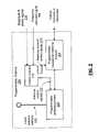
- FIG. 4is a schematic block diagram of an embodiment of a programmable antenna in accordance with the present invention.
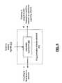
- a programmable antenna 225is presented that includes an antenna having a fixed antenna element 202 and a programmable antenna element 200 .
- the programmable antenna 225further includes a control module 210 and an impedance matching network 206 .
- the programmable antenna 225is tunable to one of a plurality of resonant frequencies in response to a frequency selection signal 169 .
- the programmable antenna element 200is coupled to the fixed antenna element 202 and is tunable to a particular resonant frequency in response to one or more antenna control signals 212 .
- programmable antenna 225can be dynamically tuned to a particular carrier frequency or sequence of carrier frequencies of a transmitted RF signal and/or of a received RF signal.
- the fixed antenna element 202has a resonant frequency or center frequency of operation that is dependent upon the physical dimensions of the fixed antenna element, such as a length of a one-quarter wavelength antenna element or other dimension.
- Programmable antenna element 200modifies the “effective” length or dimension of the overall antenna by selectively adding or subtracting from the reactance of the programmable antenna element 200 to conform to changes in the selected frequency and the corresponding changes in wavelength.
- the fixed antenna element 202can include one or more elements in combination that each can be a dipole, loop, annular slot or other slot configuration, rectangular aperture, circular aperture, line source, helical element or other element or antenna configuration.
- the programmable antenna element 200can be implemented with an adjustable impedance having a reactance, and optionally a resistive component, that each can be programmed to any one of a plurality of values. Further details regarding additional implementations of programmable antenna element 200 are presented in conjunction with FIGS. 6-11 and 14 that follow.
- Programmable antenna 225optionally includes impedance matching network 206 that couples the programmable antenna 225 to and from a receiver or transmitter, either directly or through a transmission line.
- Impedance matching network 225attempts to maximize the power transfer between the antenna and the receiver or between the transmitter and the antenna, to minimize reflections and/or standing wave ratio, and/or to bridge the impedance of the antenna to the receiver and/or transmitter or vice versa.
- the impedance matching network 206includes a transformer such as a balun transformer, an L-section, pi-network, t-network or other impedance network that performs the function of impedance matching.
- Control module 210generates the one or more antenna control signals 212 in response to a frequency selection signal.
- control module 210produces antenna control signals 212 to command the programmable antenna element to modify its impedance in accordance with a desired resonant frequency or the particular carrier frequency that is indicated by the frequency selection signal 169 .
- the control moduleIn the event that frequency selection signal indicates a particular carrier frequency corresponding to a particular 802.11 channel of the 2.4 GHz band, the control module generates antenna control signals 212 that command the programmable antenna element 200 to adjust its impedance such that the overall resonant frequency of the programmable antenna, including both the fixed antenna element 202 and programmable antenna element 200 is equal to, substantially equal to or as close as possible to the selected carrier frequency.
- the set of possible carrier frequenciesis known in advance and the control module 210 is preprogrammed with the particular antenna control signals 212 that correspond to each carrier frequency, so that when a particular carrier frequency is selected, logic or other circuitry or programming such as via a look-up table can be used to retrieve the particular antenna control signals required for the selected frequency.
- the control module 210based on equations derived from impedance network principles that will be apparent to one of ordinary skill in the art when presented the disclosure herein, calculates the particular impedance that is required of programmable antenna network 200 and generates antenna control commands 212 to implement this particular impedance.
- control module 210includes a processing module that performs various processing steps to implement the functions and features described herein.
- a processing modulecan be implemented using a shared processing device, individual processing devices, or a plurality of processing devices and may further include memory.
- a processing devicemay be a microprocessor, micro-controller, digital signal processor, microcomputer, central processing unit, field programmable gate array, programmable logic device, state machine, logic circuitry, analog circuitry, digital circuitry, and/or any device that manipulates signals (analog and/or digital) based on operational instructions.
- the memorymay be a single memory device or a plurality of memory devices.
- Such a memory devicemay be a read-only memory, random access memory, volatile memory, non-volatile memory, static memory, dynamic memory, flash memory, and/or any device that stores digital information.
- the control moduleimplements one or more of its functions via a state machine, analog circuitry, digital circuitry, and/or logic circuitry
- the memory storing the corresponding operational instructionsis embedded with the circuitry comprising the state machine, analog circuitry, digital circuitry, and/or logic circuitry.
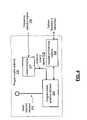
- FIG. 5is a schematic block diagram of an embodiment of a programmable antenna in accordance with the present invention.
- a programmable antenna 225 ′is shown that includes many common elements of programmable antenna 225 that are referred to by common reference numerals.
- programmable antenna 225 ′includes a programmable impedance matching network 204 that is tunable in response to one or more matching network control signals 214 generated by control module 210 , to provide a substantially constant load impedance. In this fashion, changes to the overall impedance of the programmable antenna caused by variations in the impedance of the programmable antenna element 200 can be compensated by adjusting the programmable impedance matching network 204 at the same time.
- control module 210can optionally adjust the impedance of programmable impedance matching network 204 to control the magnitude and phase of the antenna current of the programmable antenna based on magnitude and phase signals 216 , or to adjust the magnitude and phase of the antenna current received from the programmable antenna to support applications such as implementation of programmable antenna 225 ′ as part of a phased array antenna system.
- control module 210can be implemented with a processing device that retrieves the particular matching network control signals 214 in response to the particular frequency, magnitude and/or phase that are selected via frequency selection signal 169 and magnitude and phase signals 216 or calculates the particular matching network control signals 214 in real-time based on network equations and the particular frequency, magnitude and/or phase that are selected.
- FIGS. 12-14Further additional implementations of programmable impedance matching network 204 are presented in conjunction with FIGS. 12-14 .
- FIG. 6is a schematic block diagram of an embodiment of a programmable antenna element in accordance with the present invention.
- programmable antenna element 200is shown that includes an adjustable impedance 290 that is adjustable in response to antenna control signal 212 .
- Adjustable impedance 290is a complex impedance with an adjustable reactance and optionally a resistive component that is also adjustable.
- Adjustable impedancecan include at least one adjustable reactive element such as an adjustable inductor, an adjustable capacitor, an adjustable tank circuit, an adjustable transformer such as a balun transformer or other adjustable impedance network or network element.
- FIG. 7is a schematic block diagram of an embodiment of an adjustable impedance in accordance with the present invention.
- An adjustable impedance 220is shown that includes a plurality of fixed network elements Z 1 , Z 2 , Z 3 , . . . Z n such as resistors, or reactive network elements such as capacitors, and/or inductors.
- a switching network 230selectively couples the plurality of fixed network elements in response to one or more control signals 252 , such as antenna control signals 212 . In operation, the switching network 230 selects at least one of the plurality of fixed reactive network elements and that deselects the remaining ones of the plurality of fixed reactive network elements in response to the control signals 252 .
- switching network 230operates to couple one of the plurality of taps to terminal B.
- the impedance between terminals A and Bis adjustable to include a total impedance Z 1 , Z 1 +Z 2 , Z 1 +Z 2 +Z 3 , etc, based on the tap selected.
- Choosing the fixed network elements Z 1 , Z 2 , Z 3 , . . . Z n to be a plurality of inductorsallows the adjustable impedance 220 to implement an adjustable inductor having a range from (Z 1 to Z 1 +Z 2 +Z 3 + . . . +Z n ).
- choosing the fixed network elements Z 1 , Z 2 , Z 3 , . . . Z nto be a plurality of capacitors, allows the adjustable impedance 220 to implement an adjustable capacitor, etc.
- FIG. 8is a schematic block diagram of an embodiment of an adjustable impedance in accordance with the present invention.
- An adjustable impedance 221is shown that includes a plurality of group A fixed network elements Z 1 , Z 2 , Z 3 , . . . Z n and group B fixed network elements Z a , Z b , Z c , . . . Z m such as resistors, or reactive network elements such as capacitors, and/or inductors.
- a switching network 231selectively couples the plurality of fixed network elements in response to one or more control signals 252 , such as antenna control signals 212 to form a parallel combination of two adjustable impedances.
- the switching network 231selects at least one of the plurality of fixed reactive network elements and that deselects the remaining ones of the plurality of fixed reactive network elements in response to the control signals 252 .
- switching network 231operates to couple one of the plurality of taps from the group A impedances to one of the plurality of taps of the group B impedances to the terminal B.
- FIG. 9is a schematic block diagram of an embodiment of an adjustable impedance in accordance with the present invention.
- An adjustable impedance 222is shown that includes a plurality of group A fixed network elements Z 1 , Z 2 , Z 3 , . . . Z n and group B fixed network elements Z a , Z b , Z c , . . . Z m such as resistors, or reactive network elements such as capacitors, and/or inductors.
- a switching network 232selectively couples the plurality of fixed network elements in response to one or more control signals 252 , such as antenna control signals 212 to form a series combination of two adjustable impedances.
- the switching network 232selects at least one of the plurality of fixed reactive network elements and that deselects the remaining ones of the plurality of fixed reactive network elements in response to the control signals 252 .
- switching network 232operates to couple one of the plurality of taps from the group A impedances to the group B impedances and one of the plurality of taps of the group B impedances to the terminal B.
- FIG. 10is a schematic block diagram of an embodiment of an adjustable impedance in accordance with the present invention.
- An adjustable impedance 223is shown that includes a plurality of fixed network elements Z 1 , Z 2 , Z 3 , . . . Z n such as resistors, or reactive network elements such as capacitors, and/or inductors.
- a switching network 233selectively couples the plurality of fixed network elements in response to one or more control signals 252 , such as antenna control signals 212 . In operation, the switching network 233 selects at least one of the plurality of fixed reactive network elements and that deselects the remaining ones of the plurality of fixed reactive network elements in response to the control signals 252 .
- switching network 233operates to couple one of the plurality of taps of the top legs of the selected elements to terminal A and the corresponding bottom legs of the selected elements to terminal B.
- the impedance between terminals A and Bis adjustable to include a total impedance that is the parallel combination of the selected fixed impedances.
- Choosing the fixed network elements Z 1 , Z 2 , Z 3 , . . . Z n to be a plurality of inductancesallows the adjustable impedance 220 to implement an adjustable inductor, from the range from the parallel combination of (Z 1 , Z 2 , Z 3 , . . . Z n ) to MAX(Z 1 , Z 2 , Z 3 . . . Z n ).
- the fixed network elements Z 1 , Z 2 , Z 3 , . . . Z ncan be chosen as a plurality of capacitances.
- FIG. 11is a schematic block diagram of an embodiment of an adjustable impedance in accordance with the present invention.
- An adjustable impedance 224is shown that includes a plurality of group A fixed network elements Z 1 , Z 2 , Z 3 , . . . Z n and group B fixed network elements Z a , Z b , Z c , . . . Z m such as resistors, or reactive network elements such as capacitors, and/or inductors.
- a switching network 234selectively couples the plurality of fixed network elements in response to one or more control signals 252 , such as antenna control signals 212 to form a series combination of two adjustable impedances.
- the switching network 234selects at least one of the plurality of fixed reactive network elements and that deselects the remaining ones of the plurality of fixed reactive network elements in response to the control signals 252 .
- switching network 232operates to couple a selected parallel combination of impedances from the group A in series with a selected parallel combination of group B impedances.
- the impedance between terminals A and Bis adjustable and can be to form a series circuit such as series tank circuit having a total impedance equal to the series combination between a group A impedance Z A and a Group B impedance Z B , based on the taps selected.
- FIG. 12is a schematic block diagram of an embodiment of a programmable impedance matching network in accordance with the present invention.
- a programmable impedance matching network 240is shown that includes a plurality of adjustable impedances 290 , responsive to matching control signals 214 .
- each of the adjustable impedances 290can be implemented in accordance with any of the adjustable impedances discussed in association with the impedances used to implement programmable antenna element 200 discussed in FIGS. 7-11 , with the control signals 252 being supplied by matching network control signal 214 , instead of antenna control signals 212 .
- a t-network configurationis implemented with three adjustable impedances, however, one or more these adjustable impedances can alternatively be replaced by an open-circuit or short circuit to produce other configurations including an L-section matching network. Further, one or more of the adjustable impedances 290 can be replaced by fixed impedances, such as resistors, or fixed reactive network elements.
- FIG. 13is a schematic block diagram of an embodiment of a programmable impedance matching network in accordance with the present invention.
- a programmable impedance matching network 242is shown that includes a plurality of adjustable impedances 290 , responsive to matching control signals 214 .
- each of the adjustable impedances 290can be implemented in accordance with any of the adjustable impedances discussed in association with the impedances used to implement programmable antenna element 200 discussed in FIGS. 7-11 , with the control signals 252 being supplied by matching network control signal 214 , instead of antenna control signals 212 .
- a pi-network configurationis implemented with three adjustable impedances, however, one or more these adjustable impedances can alternatively be replaced by an open-circuit or short circuit to produce other configurations. Further, one or more of the adjustable impedances 290 can be replaced by fixed impedances, such as resistors, or fixed reactive network elements.
- FIG. 14is a schematic block diagram of an embodiment of an adjustable transformer in accordance with the present invention.
- An adjustable transformeris shown that can be used in either the implementation of programmable antenna element 200 , with control signals 252 being supplied by antenna control signals 212 .
- adjustable transformer 250can be used to implement all or part of the programmable impedance matching network 204 , with control signals 252 being supplied by matching network control signals 214 .
- multi-tap inductors 254 and 256are magnetically coupled.
- Switching network 235controls the tap selection for terminals A and B (and optionally to ground) to produce a transformer, such as a balun transformer or other voltage/current/impedance transforming device with controlled impedance matching characteristics and optionally with controlled bridging.
- FIG. 15is a schematic block diagram of an RF transceiver in accordance with the present invention.
- An RF transceiveris presented that includes many common elements from RF transceiver 125 that are referred to by common reference numerals.
- an RF transmission and reception systemsare disclosed that operate with frequency hopping.
- a frequency hop modulegenerates frequency selection signal 169 that indicates a sequence of selected carrier frequencies.
- An RF transmitter 129generates an outbound RF signal 170 at the sequence of selected carrier frequencies.
- Programmable antenna 173such as programmable antenna 225 or 225 ′ tunes to each frequency of the sequence of selected carrier frequencies, based on the frequency selection signal 169 , to transmit the RF signal.
- Programmable antenna 171such as programmable antenna 225 or 225 ′, tunes to each frequency of the sequence of selected carrier frequencies, based on the frequency selection signal 169 and that receives an inbound RF signal 152 having the sequence of selected carrier frequencies.
- An RF receiver 127demodulates the RF signal 127 to produce inbound data 160 .
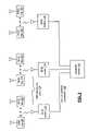
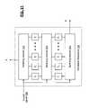
- FIG. 16is a schematic block diagram of an RF transmission system in accordance with the present invention.
- An RF transmission system 260is disclosed that includes many common elements from RF transmitter 129 that are referred to by common reference numerals.
- RF transmission system 260includes either a plurality of RF transmitters or a plurality of RF transmitter front ends 150 that generate a plurality of RF signals 294 - 296 at a selected carrier frequency in response to a frequency selection signal 169 .
- a plurality of programmable antennas 173such as antennas 225 or 225 ′, are each tuned to the selected carrier frequency, in response to the frequency selection signal, to transmit a corresponding one of the plurality of RF signals 294 - 296 .
- the plurality of RF transmitter front ends 150are implemented as part of a multi-input multi-output (MIMO) transceiving system that broadcasts multiple signals that are recombined in the receiver.
- MIMOmulti-input multi-output
- antennas 173can be spaced with physical diversity.
- the plurality of RF transmitter front-endsare implemented as part of a polarization diversity transceiving system that broadcasts multiple signals at different polarizations by antennas 173 configured at a plurality of different polarizations.
- FIG. 17is a schematic block diagram of an RF reception system in accordance with the present invention.
- An RF reception system 260is disclosed that includes many common elements from RF receiver 127 that are referred to by common reference numerals.
- a plurality of programmable antennas 171are each tuned to a selected carrier frequency in response to a frequency selection signal 169 .
- the plurality of programmable antennasreceive RF signals 297 - 299 having the selected carrier frequency.
- a plurality of RF receiversinclude RF front-ends 140 and down conversion modules 142 , to demodulate the RF signal 297 - 299 into demodulated signal 287 - 289 .
- a recombination module 262produces a recombined data signal, such as inbound data 160 from the demodulated signals 287 - 289 .
- the plurality of RF front ends 140are implemented as part of a multi-input multi-output (MIMO) transceiving system that broadcasts multiple signals that are recombined in the receiver.
- MIMOmulti-input multi-output
- antennas 171can be spaced with physical diversity.
- the plurality of RF front-ends 140are implemented as part of a polarization diversity transceiving system that broadcasts multiple signals at different polarizations that are received by antennas 171 , which are configured at a plurality of different polarizations.
- Recombination module 262can include a processing module that performs various processing steps to implement the functions and features described herein.
- a processing modulecan be implemented using a shared processing device, individual processing devices, or a plurality of processing devices and may further include memory.
- Such a processing devicemay be a microprocessor, micro-controller, digital signal processor, microcomputer, central processing unit, field programmable gate array, programmable logic device, state machine, logic circuitry, analog circuitry, digital circuitry, and/or any device that manipulates signals (analog and/or digital) based on operational instructions.
- the memorymay be a single memory device or a plurality of memory devices.
- Such a memory devicemay be a read-only memory, random access memory, volatile memory, non-volatile memory, static memory, dynamic memory, flash memory, and/or any device that stores digital information.
- the processing moduleimplements one or more of its functions via a state machine, analog circuitry, digital circuitry, and/or logic circuitry
- the memory storing the corresponding operational instructionsis embedded with the circuitry comprising the state machine, analog circuitry, digital circuitry, and/or logic circuitry.
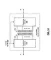
- FIG. 18is a schematic block diagram of a phased array antenna system 282 system in accordance with the present invention.
- phased array 282includes a plurality of programmable antennas 173 , such as programmable antennas 225 or 225 ′, that are driven by an RF signal 283 from transmitter 284 , such as RF transmitter 129 .
- Transmitter 284further includes frequency control module 175 .
- Each of the plurality of programmable antennas 173is tuned to a selected carrier frequency in response to a frequency selection signal 169 .
- each of the plurality of programmable antennashas an antenna current that is adjusted in response to magnitude and phase adjust signals 216 .
- the plurality of programmable antennascombine to produce a controlled beam shape, such as with a main lobe in a selected direction, or a null in a selected direction.
- a controlled beam shapesuch as with a main lobe in a selected direction, or a null in a selected direction.
- nullthe radiation from the antenna in the selected direction is attenuated significantly, by an order or magnitude or more, in order to attenuate interference with another station set or to produce greater radiated output in the direction of the main lobe.
- the magnitudes and phases adjustments for each of the antennascan be calculated in many ways to achieve the desired beam shape, such as the manner presented in Stuckman & Hill, Method of Null Steering in Phased Array Antenna Systems, Electronics Letters, Vol. 26, No. 15, Jul. 19, 1990, pp. 1216-1218.
- FIG. 19is a schematic block diagram of a phased array antenna system 296 system in accordance with the present invention.
- phased array 296includes a plurality of programmable antennas 173 , such as programmable antennas 225 or 225 ′, that combine to generate a plurality of RF signal 292 to receiver 294 , such as RF receiver 127 .
- Receiver 294further includes frequency control module 175 .
- Each of the plurality of programmable antennas 173is tuned to a selected carrier frequency in response to a frequency selection signal 169 .
- each of the plurality of programmable antennashas an antenna current that is adjusted in response to magnitude and phase adjust signals 216 .
- the plurality of programmable antennascombine to produce a controlled beam shape, such as with a main lobe in a selected direction, or a null in a selected direction.
- a controlled beam shapesuch as with a main lobe in a selected direction, or a null in a selected direction.
- the magnitudes and phases adjustments for each of the antennascan be calculated in many ways to achieve the desired beam shape.
- FIG. 20is a flowchart representation of a method in accordance with an embodiment of the present invention. In particular a method is presented for use with one or more features or functions presented in conjunction with FIGS. 1-19 .
- a frequency selection signalis receiver.
- an antenna control signalis generated to tune a programmable antenna element to a selected frequency, based on the frequency selection signal.
- at least one matching network control signalis generated, based on the frequency selection signal, to provide a substantially constant load impedance for a programmable antenna that includes the programmable antenna element.
- the at least one matching network control signalis further generated in response to a selected magnitude of an antenna current of the programmable antenna and a selected phase of the antenna current.
- the at least one matching network control signalcan be generated to tune an adjustable balun transformer, to tune at least one adjustable reactive network element, to control a switching network for selectively coupling a plurality of fixed reactive network elements, to select at least one of the plurality of fixed reactive network elements and deselect the remaining ones of the plurality of fixed reactive network elements and/or to tune a plurality of adjustable reactive network elements.
- FIG. 21is a flowchart representation of a method in accordance with an embodiment of the present invention. In particular, a method is presented for use in conjunction with one or more features and function discussed in conjunction with FIGS. 1-20 .
- a frequency hopping sequence of selected carrier frequenciesis generated.
- an antenna control signalis generated to tune a programmable antenna element to each carrier frequency of the frequency hopping sequence.
- FIG. 22is a flowchart representation of a method in accordance with an embodiment of the present invention.
- a methodis presented for use in conjunction with one or more features discussed in conjunction with FIGS. 1-20 , and that includes common elements from FIG. 21 that are referred to by common reference numerals.
- this methodincludes step 414 for generating at least one matching network control signal, based on each carrier frequency, to control a programmable impedance matching network to provide a substantially constant load impedance for a programmable antenna that includes the programmable antenna element.
- At least one matching network control signalis further generated in response to a selected magnitude of an antenna current of the programmable antenna and a selected phase of the antenna current the at least one matching network control signal is further generated in response to a selected magnitude of an antenna current of the programmable antenna and a selected phase of the antenna current.
- the at least one matching network control signalcan be generated to tune an adjustable balun transformer, to tune at least one adjustable reactive network element, to control a switching network for selectively coupling a plurality of fixed reactive network elements, to select at least one of the plurality of fixed reactive network elements and deselect the remaining ones of the plurality of fixed reactive network elements and/or to tune a plurality of adjustable reactive network elements.
- FIG. 23is a flowchart representation of a method in accordance with an embodiment of the present invention. In particular, a method is presented for use with one or more features or function discussed in conjunction with FIGS. 1-22 .
- a frequency selection signalis generated.
- a plurality of antenna control signalsare generated to tune a plurality of programmable antenna elements to a selected carrier frequency in response to the frequency selection signal.
- FIG. 24is a flowchart representation of a method in accordance with an embodiment of the present invention.
- a methodis presented for use with one or more features or function discussed in conjunction with FIGS. 1-22 , and that includes elements from FIG. 23 that are referred to by common reference numerals.
- the methodincludes step 424 for generating at least one matching network control signal, based on the frequency selection signal, to control a programmable impedance matching network to provide a substantially constant load impedance for a programmable antenna that includes one of the plurality of the programmable antenna elements.
- the at least one matching network control signalis further generated in response to a selected magnitude of an antenna current of the programmable antenna and a selected phase of the antenna current.
- the terms “substantially” and “approximately”provides an industry-accepted tolerance for its corresponding term and/or relativity between items. Such an industry-accepted tolerance ranges from less than one percent to fifty percent and corresponds to, but is not limited to, component values, integrated circuit process variations, temperature variations, rise and fall times, and/or thermal noise. Such relativity between items ranges from a difference of a few percent to magnitude differences.
- the term(s) “coupled to” and/or “coupling” and/orincludes direct coupling between items and/or indirect coupling between items via an intervening item (e.g., an item includes, but is not limited to, a component, an element, a circuit, and/or a module) where, for indirect coupling, the intervening item does not modify the information of a signal but may adjust its current level, voltage level, and/or power level.
- an intervening iteme.g., an item includes, but is not limited to, a component, an element, a circuit, and/or a module
- inferred couplingi.e., where one element is coupled to another element by inference
- the term “operable to”indicates that an item includes one or more of power connections, input(s), output(s), etc., to perform one or more its corresponding functions and may further include inferred coupling to one or more other items.
- the term “associated with”,includes direct and/or indirect coupling of separate items and/or one item being embedded within another item.
- the term “compares favorably”,indicates that a comparison between two or more items, signals, etc., provides a desired relationship. For example, when the desired relationship is that signal 1 has a greater magnitude than signal 2 , a favorable comparison may be achieved when the magnitude of signal 1 is greater than that of signal 2 or when the magnitude of signal 2 is less than that of signal 1 .
- transistors discussed abovemay be field effect transistors (FETs), as one of ordinary skill in the art will appreciate, the transistors may be implemented using any type of transistor structure including, but not limited to, bipolar, metal oxide semiconductor field effect transistors (MOSFET), N-well transistors, P-well transistors, enhancement mode, depletion mode, and zero voltage threshold (VT) transistors.
- FETsfield effect transistors
- MOSFETmetal oxide semiconductor field effect transistors
- N-well transistorsN-well transistors
- P-well transistorsP-well transistors
- enhancement modeenhancement mode
- depletion modedepletion mode
- VTzero voltage threshold
Landscapes
- Variable-Direction Aerials And Aerial Arrays (AREA)
- Transceivers (AREA)
Abstract
Description
Claims (24)
Priority Applications (3)
| Application Number | Priority Date | Filing Date | Title |
|---|---|---|---|
| US11/525,269US7639199B2 (en) | 2006-09-22 | 2006-09-22 | Programmable antenna with programmable impedance matching and methods for use therewith |
| US12/614,870US7893888B2 (en) | 2006-09-22 | 2009-11-09 | Programmable antenna with programmable impedance matching and methods for use therewith |
| US13/022,625US8106848B2 (en) | 2006-09-22 | 2011-02-07 | Programmable antenna with programmable impedance matching and methods for use therewith |
Applications Claiming Priority (1)
| Application Number | Priority Date | Filing Date | Title |
|---|---|---|---|
| US11/525,269US7639199B2 (en) | 2006-09-22 | 2006-09-22 | Programmable antenna with programmable impedance matching and methods for use therewith |
Related Child Applications (1)
| Application Number | Title | Priority Date | Filing Date |
|---|---|---|---|
| US12/614,870ContinuationUS7893888B2 (en) | 2006-09-22 | 2009-11-09 | Programmable antenna with programmable impedance matching and methods for use therewith |
Publications (2)
| Publication Number | Publication Date |
|---|---|
| US20080122723A1 US20080122723A1 (en) | 2008-05-29 |
| US7639199B2true US7639199B2 (en) | 2009-12-29 |
Family
ID=39463145
Family Applications (3)
| Application Number | Title | Priority Date | Filing Date |
|---|---|---|---|
| US11/525,269Expired - Fee RelatedUS7639199B2 (en) | 2006-09-22 | 2006-09-22 | Programmable antenna with programmable impedance matching and methods for use therewith |
| US12/614,870Expired - Fee RelatedUS7893888B2 (en) | 2006-09-22 | 2009-11-09 | Programmable antenna with programmable impedance matching and methods for use therewith |
| US13/022,625Expired - Fee RelatedUS8106848B2 (en) | 2006-09-22 | 2011-02-07 | Programmable antenna with programmable impedance matching and methods for use therewith |
Family Applications After (2)
| Application Number | Title | Priority Date | Filing Date |
|---|---|---|---|
| US12/614,870Expired - Fee RelatedUS7893888B2 (en) | 2006-09-22 | 2009-11-09 | Programmable antenna with programmable impedance matching and methods for use therewith |
| US13/022,625Expired - Fee RelatedUS8106848B2 (en) | 2006-09-22 | 2011-02-07 | Programmable antenna with programmable impedance matching and methods for use therewith |
Country Status (1)
| Country | Link |
|---|---|
| US (3) | US7639199B2 (en) |
Cited By (12)
| Publication number | Priority date | Publication date | Assignee | Title |
|---|---|---|---|---|
| US20060233221A1 (en)* | 2002-12-27 | 2006-10-19 | Luzhou Xu | Multi-antenna solution for mobile handset |
| US20080076476A1 (en)* | 2006-09-22 | 2008-03-27 | Broadcom Corporation, A California Corporation | RF transceiver with a plurality of programmable antennas and methods for use therewith |
| US20100053018A1 (en)* | 2006-09-22 | 2010-03-04 | Broadcom Corporation | Programmable antenna with programmable impedance matching and methods for use therewith |
| US20110237238A1 (en)* | 2010-03-26 | 2011-09-29 | Microsoft Corporation | Cellular service with improved service availability |
| US20120055988A1 (en)* | 2010-09-03 | 2012-03-08 | Hand Held Products, Inc. | Encoded information reading terminal with multi-band antenna |
| US20120146425A1 (en)* | 2010-12-14 | 2012-06-14 | Samsung Electro-Mechanics Co., Ltd. | Wireless power transmission/reception apparatus and method |
| CN103606003A (en)* | 2013-12-05 | 2014-02-26 | 上海坤锐电子科技有限公司 | Automatic detuning voltage stabilizing circuit for radio frequency identification tag chip |
| US9057259B2 (en) | 2013-02-01 | 2015-06-16 | Harris Corporation | Hydrocarbon resource recovery apparatus including a transmission line with fluid tuning chamber and related methods |
| US9115576B2 (en) | 2012-11-14 | 2015-08-25 | Harris Corporation | Method for producing hydrocarbon resources with RF and conductive heating and related apparatuses |
| US9157305B2 (en) | 2013-02-01 | 2015-10-13 | Harris Corporation | Apparatus for heating a hydrocarbon resource in a subterranean formation including a fluid balun and related methods |
| US9267365B2 (en) | 2013-02-01 | 2016-02-23 | Harris Corporation | Apparatus for heating a hydrocarbon resource in a subterranean formation providing an adjustable liquid coolant and related methods |
| US9404352B2 (en) | 2013-02-01 | 2016-08-02 | Harris Corporation | Transmission line segment coupler defining fluid passage ways and related methods |
Families Citing this family (218)
| Publication number | Priority date | Publication date | Assignee | Title |
|---|---|---|---|---|
| US8744384B2 (en) | 2000-07-20 | 2014-06-03 | Blackberry Limited | Tunable microwave devices with auto-adjusting matching circuit |
| US8064188B2 (en) | 2000-07-20 | 2011-11-22 | Paratek Microwave, Inc. | Optimized thin film capacitors |
| US9406444B2 (en) | 2005-11-14 | 2016-08-02 | Blackberry Limited | Thin film capacitors |
| US7711337B2 (en) | 2006-01-14 | 2010-05-04 | Paratek Microwave, Inc. | Adaptive impedance matching module (AIMM) control architectures |
| US8325097B2 (en) | 2006-01-14 | 2012-12-04 | Research In Motion Rf, Inc. | Adaptively tunable antennas and method of operation therefore |
| US8125399B2 (en)* | 2006-01-14 | 2012-02-28 | Paratek Microwave, Inc. | Adaptively tunable antennas incorporating an external probe to monitor radiated power |
| US7714676B2 (en) | 2006-11-08 | 2010-05-11 | Paratek Microwave, Inc. | Adaptive impedance matching apparatus, system and method |
| US7535312B2 (en) | 2006-11-08 | 2009-05-19 | Paratek Microwave, Inc. | Adaptive impedance matching apparatus, system and method with improved dynamic range |
| US8299867B2 (en)* | 2006-11-08 | 2012-10-30 | Research In Motion Rf, Inc. | Adaptive impedance matching module |
| US8249573B2 (en)* | 2006-12-29 | 2012-08-21 | Broadcom Corporation | Method and system for software defined power amplifier for multi-band applications |
| US7917104B2 (en) | 2007-04-23 | 2011-03-29 | Paratek Microwave, Inc. | Techniques for improved adaptive impedance matching |
| US8213886B2 (en) | 2007-05-07 | 2012-07-03 | Paratek Microwave, Inc. | Hybrid techniques for antenna retuning utilizing transmit and receive power information |
| US8249678B2 (en)* | 2007-09-28 | 2012-08-21 | Kyocera Corporation | Wireless communication device with configurable antenna |
| US7991363B2 (en) | 2007-11-14 | 2011-08-02 | Paratek Microwave, Inc. | Tuning matching circuits for transmitter and receiver bands as a function of transmitter metrics |
| EP2269267B1 (en)* | 2008-04-28 | 2017-12-13 | Wispry, Inc. | Tunable duplexing antenna and methods |
| US8072285B2 (en) | 2008-09-24 | 2011-12-06 | Paratek Microwave, Inc. | Methods for tuning an adaptive impedance matching network with a look-up table |
| US8472888B2 (en) | 2009-08-25 | 2013-06-25 | Research In Motion Rf, Inc. | Method and apparatus for calibrating a communication device |
| US9026062B2 (en) | 2009-10-10 | 2015-05-05 | Blackberry Limited | Method and apparatus for managing operations of a communication device |
| US20110116424A1 (en)* | 2009-11-19 | 2011-05-19 | Hand Held Products, Inc. | Network-agnostic encoded information reading terminal |
| TWI437844B (en)* | 2009-12-16 | 2014-05-11 | Realtek Semiconductor Corp | Apparatus and method for receiving a plurality of broadcasting signals |
| US8803631B2 (en) | 2010-03-22 | 2014-08-12 | Blackberry Limited | Method and apparatus for adapting a variable impedance network |
| SG184929A1 (en) | 2010-04-20 | 2012-11-29 | Paratek Microwave Inc | Method and apparatus for managing interference in a communication device |
| WO2012027703A2 (en)* | 2010-08-26 | 2012-03-01 | Wispry, Inc. | Tunable radio front end and methods |
| TWI431935B (en) | 2010-09-28 | 2014-03-21 | Htc Corp | Antenna module |
| US9379454B2 (en) | 2010-11-08 | 2016-06-28 | Blackberry Limited | Method and apparatus for tuning antennas in a communication device |
| US20120203620A1 (en) | 2010-11-08 | 2012-08-09 | Douglas Howard Dobyns | Techniques For Wireless Communication Of Proximity Based Marketing |
| WO2012079084A2 (en) | 2010-12-10 | 2012-06-14 | Wispry, Inc. | Mems tunable notch filter frequency automatic control loop systems and methods |
| US8712340B2 (en) | 2011-02-18 | 2014-04-29 | Blackberry Limited | Method and apparatus for radio antenna frequency tuning |
| US8655286B2 (en) | 2011-02-25 | 2014-02-18 | Blackberry Limited | Method and apparatus for tuning a communication device |
| US8556178B2 (en)* | 2011-03-04 | 2013-10-15 | Hand Held Products, Inc. | RFID devices using metamaterial antennas |
| US8929809B2 (en) | 2011-03-22 | 2015-01-06 | Radeum, Inc. | Techniques for wireless communication of proximity based content |
| US8880100B2 (en) | 2011-03-23 | 2014-11-04 | Radium, Inc. | Proximity based social networking |
| US8626083B2 (en) | 2011-05-16 | 2014-01-07 | Blackberry Limited | Method and apparatus for tuning a communication device |
| US8594584B2 (en) | 2011-05-16 | 2013-11-26 | Blackberry Limited | Method and apparatus for tuning a communication device |
| US9769826B2 (en) | 2011-08-05 | 2017-09-19 | Blackberry Limited | Method and apparatus for band tuning in a communication device |
| US8699965B2 (en)* | 2011-11-29 | 2014-04-15 | Symbol Technologies, Inc. | Low loss quarter wave radio frequency relay switch apparatus and method |
| US20130147680A1 (en)* | 2011-12-13 | 2013-06-13 | Cheng Uei Precision Industry Co., Ltd. | Antenna impedance matching method |
| US9715608B2 (en)* | 2011-12-19 | 2017-07-25 | Symbol Technologies, Llc | Method and apparatus for improving radio frequency identification coverage |
| US9436857B2 (en) | 2012-01-16 | 2016-09-06 | Hand Held Products, Inc. | Encoded information reading system including RFID reading device having multiple antennas |
| US20130187828A1 (en) | 2012-01-24 | 2013-07-25 | Ethertronics, Inc. | Tunable matching network for antenna systems |
| US9325062B2 (en)* | 2012-01-24 | 2016-04-26 | Ethertronics, Inc. | High speed tunable matching network for antenna systems |
| US8948889B2 (en) | 2012-06-01 | 2015-02-03 | Blackberry Limited | Methods and apparatus for tuning circuit components of a communication device |
| US9853363B2 (en) | 2012-07-06 | 2017-12-26 | Blackberry Limited | Methods and apparatus to control mutual coupling between antennas |
| US9246223B2 (en) | 2012-07-17 | 2016-01-26 | Blackberry Limited | Antenna tuning for multiband operation |
| US9413066B2 (en) | 2012-07-19 | 2016-08-09 | Blackberry Limited | Method and apparatus for beam forming and antenna tuning in a communication device |
| US9350405B2 (en) | 2012-07-19 | 2016-05-24 | Blackberry Limited | Method and apparatus for antenna tuning and power consumption management in a communication device |
| US9362891B2 (en) | 2012-07-26 | 2016-06-07 | Blackberry Limited | Methods and apparatus for tuning a communication device |
| JP2014064148A (en)* | 2012-09-20 | 2014-04-10 | Sharp Corp | Radio circuit and radio circuit control method |
| US9113347B2 (en) | 2012-12-05 | 2015-08-18 | At&T Intellectual Property I, Lp | Backhaul link for distributed antenna system |
| US10009065B2 (en) | 2012-12-05 | 2018-06-26 | At&T Intellectual Property I, L.P. | Backhaul link for distributed antenna system |
| US9374113B2 (en) | 2012-12-21 | 2016-06-21 | Blackberry Limited | Method and apparatus for adjusting the timing of radio antenna tuning |
| US10404295B2 (en) | 2012-12-21 | 2019-09-03 | Blackberry Limited | Method and apparatus for adjusting the timing of radio antenna tuning |
| US20150236798A1 (en)* | 2013-03-14 | 2015-08-20 | Peregrine Semiconductor Corporation | Methods for Increasing RF Throughput Via Usage of Tunable Filters |
| US9999038B2 (en) | 2013-05-31 | 2018-06-12 | At&T Intellectual Property I, L.P. | Remote distributed antenna system |
| US9525524B2 (en) | 2013-05-31 | 2016-12-20 | At&T Intellectual Property I, L.P. | Remote distributed antenna system |
| US8897697B1 (en) | 2013-11-06 | 2014-11-25 | At&T Intellectual Property I, Lp | Millimeter-wave surface-wave communications |
| US10028277B2 (en)* | 2013-11-20 | 2018-07-17 | Cyborg Inc. | Variable frequency data transmission |
| US9209902B2 (en) | 2013-12-10 | 2015-12-08 | At&T Intellectual Property I, L.P. | Quasi-optical coupler |
| CN104779966A (en)* | 2014-01-15 | 2015-07-15 | 启碁科技股份有限公司 | Wireless communication device |
| US9692101B2 (en) | 2014-08-26 | 2017-06-27 | At&T Intellectual Property I, L.P. | Guided wave couplers for coupling electromagnetic waves between a waveguide surface and a surface of a wire |
| US9621227B2 (en) | 2014-08-29 | 2017-04-11 | Freelinc Technologies | Proximity boundary based communication using radio frequency (RF) communication standards |
| KR102375696B1 (en)* | 2014-09-05 | 2022-03-17 | 한국전자통신연구원 | Method and appartus for modulating baseband signal in beam space multi-input mult-output |
| US9641231B2 (en)* | 2014-09-05 | 2017-05-02 | Electronics And Telecommunications Research Institute | Method and appartus for modulating baseband signal in beam space multi-input multi-output |
| KR102375697B1 (en)* | 2014-09-12 | 2022-03-17 | 한국전자통신연구원 | Method and appartus for modulating baseband signal in beam space multi-input mult-output |
| US9692492B2 (en)* | 2014-09-12 | 2017-06-27 | Electronics And Telecommunications Research Institute | Method and apparatus for modulating baseband signal in beam space multi-input multi-output, and method for receiving therein |
| US9768833B2 (en) | 2014-09-15 | 2017-09-19 | At&T Intellectual Property I, L.P. | Method and apparatus for sensing a condition in a transmission medium of electromagnetic waves |
| US10063280B2 (en) | 2014-09-17 | 2018-08-28 | At&T Intellectual Property I, L.P. | Monitoring and mitigating conditions in a communication network |
| US9628854B2 (en) | 2014-09-29 | 2017-04-18 | At&T Intellectual Property I, L.P. | Method and apparatus for distributing content in a communication network |
| US9615269B2 (en) | 2014-10-02 | 2017-04-04 | At&T Intellectual Property I, L.P. | Method and apparatus that provides fault tolerance in a communication network |
| US9685992B2 (en) | 2014-10-03 | 2017-06-20 | At&T Intellectual Property I, L.P. | Circuit panel network and methods thereof |
| US9503189B2 (en) | 2014-10-10 | 2016-11-22 | At&T Intellectual Property I, L.P. | Method and apparatus for arranging communication sessions in a communication system |
| US9973299B2 (en) | 2014-10-14 | 2018-05-15 | At&T Intellectual Property I, L.P. | Method and apparatus for adjusting a mode of communication in a communication network |
| US9762289B2 (en) | 2014-10-14 | 2017-09-12 | At&T Intellectual Property I, L.P. | Method and apparatus for transmitting or receiving signals in a transportation system |
| US9577306B2 (en) | 2014-10-21 | 2017-02-21 | At&T Intellectual Property I, L.P. | Guided-wave transmission device and methods for use therewith |
| US9780834B2 (en) | 2014-10-21 | 2017-10-03 | At&T Intellectual Property I, L.P. | Method and apparatus for transmitting electromagnetic waves |
| US9769020B2 (en) | 2014-10-21 | 2017-09-19 | At&T Intellectual Property I, L.P. | Method and apparatus for responding to events affecting communications in a communication network |
| US9653770B2 (en) | 2014-10-21 | 2017-05-16 | At&T Intellectual Property I, L.P. | Guided wave coupler, coupling module and methods for use therewith |
| US9520945B2 (en) | 2014-10-21 | 2016-12-13 | At&T Intellectual Property I, L.P. | Apparatus for providing communication services and methods thereof |
| US9312919B1 (en) | 2014-10-21 | 2016-04-12 | At&T Intellectual Property I, Lp | Transmission device with impairment compensation and methods for use therewith |
| US9627768B2 (en) | 2014-10-21 | 2017-04-18 | At&T Intellectual Property I, L.P. | Guided-wave transmission device with non-fundamental mode propagation and methods for use therewith |
| US9654173B2 (en) | 2014-11-20 | 2017-05-16 | At&T Intellectual Property I, L.P. | Apparatus for powering a communication device and methods thereof |
| US9954287B2 (en) | 2014-11-20 | 2018-04-24 | At&T Intellectual Property I, L.P. | Apparatus for converting wireless signals and electromagnetic waves and methods thereof |
| US9742462B2 (en) | 2014-12-04 | 2017-08-22 | At&T Intellectual Property I, L.P. | Transmission medium and communication interfaces and methods for use therewith |
| US10340573B2 (en) | 2016-10-26 | 2019-07-02 | At&T Intellectual Property I, L.P. | Launcher with cylindrical coupling device and methods for use therewith |
| US9544006B2 (en) | 2014-11-20 | 2017-01-10 | At&T Intellectual Property I, L.P. | Transmission device with mode division multiplexing and methods for use therewith |
| US10243784B2 (en) | 2014-11-20 | 2019-03-26 | At&T Intellectual Property I, L.P. | System for generating topology information and methods thereof |
| US9461706B1 (en) | 2015-07-31 | 2016-10-04 | At&T Intellectual Property I, Lp | Method and apparatus for exchanging communication signals |
| US9800327B2 (en) | 2014-11-20 | 2017-10-24 | At&T Intellectual Property I, L.P. | Apparatus for controlling operations of a communication device and methods thereof |
| US10009067B2 (en) | 2014-12-04 | 2018-06-26 | At&T Intellectual Property I, L.P. | Method and apparatus for configuring a communication interface |
| US9997819B2 (en) | 2015-06-09 | 2018-06-12 | At&T Intellectual Property I, L.P. | Transmission medium and method for facilitating propagation of electromagnetic waves via a core |
| US9680670B2 (en) | 2014-11-20 | 2017-06-13 | At&T Intellectual Property I, L.P. | Transmission device with channel equalization and control and methods for use therewith |
| US9438319B2 (en) | 2014-12-16 | 2016-09-06 | Blackberry Limited | Method and apparatus for antenna selection |
| US10164685B2 (en) | 2014-12-31 | 2018-12-25 | Freelinc Technologies Inc. | Spatially aware wireless network |
| US10144036B2 (en) | 2015-01-30 | 2018-12-04 | At&T Intellectual Property I, L.P. | Method and apparatus for mitigating interference affecting a propagation of electromagnetic waves guided by a transmission medium |
| US9876570B2 (en) | 2015-02-20 | 2018-01-23 | At&T Intellectual Property I, Lp | Guided-wave transmission device with non-fundamental mode propagation and methods for use therewith |
| US9749013B2 (en) | 2015-03-17 | 2017-08-29 | At&T Intellectual Property I, L.P. | Method and apparatus for reducing attenuation of electromagnetic waves guided by a transmission medium |
| US9705561B2 (en) | 2015-04-24 | 2017-07-11 | At&T Intellectual Property I, L.P. | Directional coupling device and methods for use therewith |
| US10224981B2 (en) | 2015-04-24 | 2019-03-05 | At&T Intellectual Property I, Lp | Passive electrical coupling device and methods for use therewith |
| US9948354B2 (en) | 2015-04-28 | 2018-04-17 | At&T Intellectual Property I, L.P. | Magnetic coupling device with reflective plate and methods for use therewith |
| US9793954B2 (en) | 2015-04-28 | 2017-10-17 | At&T Intellectual Property I, L.P. | Magnetic coupling device and methods for use therewith |
| US9871282B2 (en) | 2015-05-14 | 2018-01-16 | At&T Intellectual Property I, L.P. | At least one transmission medium having a dielectric surface that is covered at least in part by a second dielectric |
| US9748626B2 (en) | 2015-05-14 | 2017-08-29 | At&T Intellectual Property I, L.P. | Plurality of cables having different cross-sectional shapes which are bundled together to form a transmission medium |
| US9490869B1 (en) | 2015-05-14 | 2016-11-08 | At&T Intellectual Property I, L.P. | Transmission medium having multiple cores and methods for use therewith |
| US10650940B2 (en) | 2015-05-15 | 2020-05-12 | At&T Intellectual Property I, L.P. | Transmission medium having a conductive material and methods for use therewith |
| US9917341B2 (en) | 2015-05-27 | 2018-03-13 | At&T Intellectual Property I, L.P. | Apparatus and method for launching electromagnetic waves and for modifying radial dimensions of the propagating electromagnetic waves |
| US9912381B2 (en) | 2015-06-03 | 2018-03-06 | At&T Intellectual Property I, Lp | Network termination and methods for use therewith |
| US10103801B2 (en) | 2015-06-03 | 2018-10-16 | At&T Intellectual Property I, L.P. | Host node device and methods for use therewith |
| US9866309B2 (en) | 2015-06-03 | 2018-01-09 | At&T Intellectual Property I, Lp | Host node device and methods for use therewith |
| US10812174B2 (en) | 2015-06-03 | 2020-10-20 | At&T Intellectual Property I, L.P. | Client node device and methods for use therewith |
| US9913139B2 (en) | 2015-06-09 | 2018-03-06 | At&T Intellectual Property I, L.P. | Signal fingerprinting for authentication of communicating devices |
| US9608692B2 (en) | 2015-06-11 | 2017-03-28 | At&T Intellectual Property I, L.P. | Repeater and methods for use therewith |
| US10142086B2 (en) | 2015-06-11 | 2018-11-27 | At&T Intellectual Property I, L.P. | Repeater and methods for use therewith |
| US9820146B2 (en) | 2015-06-12 | 2017-11-14 | At&T Intellectual Property I, L.P. | Method and apparatus for authentication and identity management of communicating devices |
| US9667317B2 (en) | 2015-06-15 | 2017-05-30 | At&T Intellectual Property I, L.P. | Method and apparatus for providing security using network traffic adjustments |
| US9509415B1 (en) | 2015-06-25 | 2016-11-29 | At&T Intellectual Property I, L.P. | Methods and apparatus for inducing a fundamental wave mode on a transmission medium |
| US9640850B2 (en) | 2015-06-25 | 2017-05-02 | At&T Intellectual Property I, L.P. | Methods and apparatus for inducing a non-fundamental wave mode on a transmission medium |
| US9865911B2 (en) | 2015-06-25 | 2018-01-09 | At&T Intellectual Property I, L.P. | Waveguide system for slot radiating first electromagnetic waves that are combined into a non-fundamental wave mode second electromagnetic wave on a transmission medium |
| US9628116B2 (en) | 2015-07-14 | 2017-04-18 | At&T Intellectual Property I, L.P. | Apparatus and methods for transmitting wireless signals |
| US10148016B2 (en) | 2015-07-14 | 2018-12-04 | At&T Intellectual Property I, L.P. | Apparatus and methods for communicating utilizing an antenna array |
| US9836957B2 (en) | 2015-07-14 | 2017-12-05 | At&T Intellectual Property I, L.P. | Method and apparatus for communicating with premises equipment |
| US10205655B2 (en) | 2015-07-14 | 2019-02-12 | At&T Intellectual Property I, L.P. | Apparatus and methods for communicating utilizing an antenna array and multiple communication paths |
| US9847566B2 (en) | 2015-07-14 | 2017-12-19 | At&T Intellectual Property I, L.P. | Method and apparatus for adjusting a field of a signal to mitigate interference |
| US10170840B2 (en) | 2015-07-14 | 2019-01-01 | At&T Intellectual Property I, L.P. | Apparatus and methods for sending or receiving electromagnetic signals |
| US10341142B2 (en) | 2015-07-14 | 2019-07-02 | At&T Intellectual Property I, L.P. | Apparatus and methods for generating non-interfering electromagnetic waves on an uninsulated conductor |
| US9882257B2 (en) | 2015-07-14 | 2018-01-30 | At&T Intellectual Property I, L.P. | Method and apparatus for launching a wave mode that mitigates interference |
| US10033107B2 (en) | 2015-07-14 | 2018-07-24 | At&T Intellectual Property I, L.P. | Method and apparatus for coupling an antenna to a device |
| US10044409B2 (en) | 2015-07-14 | 2018-08-07 | At&T Intellectual Property I, L.P. | Transmission medium and methods for use therewith |
| US9853342B2 (en) | 2015-07-14 | 2017-12-26 | At&T Intellectual Property I, L.P. | Dielectric transmission medium connector and methods for use therewith |
| US10320586B2 (en) | 2015-07-14 | 2019-06-11 | At&T Intellectual Property I, L.P. | Apparatus and methods for generating non-interfering electromagnetic waves on an insulated transmission medium |
| US9722318B2 (en) | 2015-07-14 | 2017-08-01 | At&T Intellectual Property I, L.P. | Method and apparatus for coupling an antenna to a device |
| US10033108B2 (en) | 2015-07-14 | 2018-07-24 | At&T Intellectual Property I, L.P. | Apparatus and methods for generating an electromagnetic wave having a wave mode that mitigates interference |
| US9793951B2 (en) | 2015-07-15 | 2017-10-17 | At&T Intellectual Property I, L.P. | Method and apparatus for launching a wave mode that mitigates interference |
| US9608740B2 (en) | 2015-07-15 | 2017-03-28 | At&T Intellectual Property I, L.P. | Method and apparatus for launching a wave mode that mitigates interference |
| US10090606B2 (en)* | 2015-07-15 | 2018-10-02 | At&T Intellectual Property I, L.P. | Antenna system with dielectric array and methods for use therewith |
| US9749053B2 (en) | 2015-07-23 | 2017-08-29 | At&T Intellectual Property I, L.P. | Node device, repeater and methods for use therewith |
| US9912027B2 (en) | 2015-07-23 | 2018-03-06 | At&T Intellectual Property I, L.P. | Method and apparatus for exchanging communication signals |
| US10784670B2 (en) | 2015-07-23 | 2020-09-22 | At&T Intellectual Property I, L.P. | Antenna support for aligning an antenna |
| US9871283B2 (en) | 2015-07-23 | 2018-01-16 | At&T Intellectual Property I, Lp | Transmission medium having a dielectric core comprised of plural members connected by a ball and socket configuration |
| US9948333B2 (en) | 2015-07-23 | 2018-04-17 | At&T Intellectual Property I, L.P. | Method and apparatus for wireless communications to mitigate interference |
| US9735833B2 (en) | 2015-07-31 | 2017-08-15 | At&T Intellectual Property I, L.P. | Method and apparatus for communications management in a neighborhood network |
| US9967173B2 (en) | 2015-07-31 | 2018-05-08 | At&T Intellectual Property I, L.P. | Method and apparatus for authentication and identity management of communicating devices |
| US10020587B2 (en) | 2015-07-31 | 2018-07-10 | At&T Intellectual Property I, L.P. | Radial antenna and methods for use therewith |
| US9904535B2 (en) | 2015-09-14 | 2018-02-27 | At&T Intellectual Property I, L.P. | Method and apparatus for distributing software |
| US10136434B2 (en) | 2015-09-16 | 2018-11-20 | At&T Intellectual Property I, L.P. | Method and apparatus for use with a radio distributed antenna system having an ultra-wideband control channel |
| US10009063B2 (en) | 2015-09-16 | 2018-06-26 | At&T Intellectual Property I, L.P. | Method and apparatus for use with a radio distributed antenna system having an out-of-band reference signal |
| US10079661B2 (en) | 2015-09-16 | 2018-09-18 | At&T Intellectual Property I, L.P. | Method and apparatus for use with a radio distributed antenna system having a clock reference |
| US10051629B2 (en) | 2015-09-16 | 2018-08-14 | At&T Intellectual Property I, L.P. | Method and apparatus for use with a radio distributed antenna system having an in-band reference signal |
| US10009901B2 (en) | 2015-09-16 | 2018-06-26 | At&T Intellectual Property I, L.P. | Method, apparatus, and computer-readable storage medium for managing utilization of wireless resources between base stations |
| US9769128B2 (en) | 2015-09-28 | 2017-09-19 | At&T Intellectual Property I, L.P. | Method and apparatus for encryption of communications over a network |
| US9729197B2 (en) | 2015-10-01 | 2017-08-08 | At&T Intellectual Property I, L.P. | Method and apparatus for communicating network management traffic over a network |
| US9882277B2 (en) | 2015-10-02 | 2018-01-30 | At&T Intellectual Property I, Lp | Communication device and antenna assembly with actuated gimbal mount |
| US9876264B2 (en) | 2015-10-02 | 2018-01-23 | At&T Intellectual Property I, Lp | Communication system, guided wave switch and methods for use therewith |
| US10665942B2 (en) | 2015-10-16 | 2020-05-26 | At&T Intellectual Property I, L.P. | Method and apparatus for adjusting wireless communications |
| US10355367B2 (en) | 2015-10-16 | 2019-07-16 | At&T Intellectual Property I, L.P. | Antenna structure for exchanging wireless signals |
| US20180034499A1 (en)* | 2016-07-28 | 2018-02-01 | Avago Technologies General Ip (Singapore) Pte.Ltd. | Reconfigurable antenna switch |
| US9912419B1 (en) | 2016-08-24 | 2018-03-06 | At&T Intellectual Property I, L.P. | Method and apparatus for managing a fault in a distributed antenna system |
| US9860075B1 (en) | 2016-08-26 | 2018-01-02 | At&T Intellectual Property I, L.P. | Method and communication node for broadband distribution |
| US10291311B2 (en) | 2016-09-09 | 2019-05-14 | At&T Intellectual Property I, L.P. | Method and apparatus for mitigating a fault in a distributed antenna system |
| US11032819B2 (en) | 2016-09-15 | 2021-06-08 | At&T Intellectual Property I, L.P. | Method and apparatus for use with a radio distributed antenna system having a control channel reference signal |
| US10135147B2 (en) | 2016-10-18 | 2018-11-20 | At&T Intellectual Property I, L.P. | Apparatus and methods for launching guided waves via an antenna |
| US10135146B2 (en) | 2016-10-18 | 2018-11-20 | At&T Intellectual Property I, L.P. | Apparatus and methods for launching guided waves via circuits |
| US10340600B2 (en) | 2016-10-18 | 2019-07-02 | At&T Intellectual Property I, L.P. | Apparatus and methods for launching guided waves via plural waveguide systems |
| US9991580B2 (en) | 2016-10-21 | 2018-06-05 | At&T Intellectual Property I, L.P. | Launcher and coupling system for guided wave mode cancellation |
| US10374316B2 (en) | 2016-10-21 | 2019-08-06 | At&T Intellectual Property I, L.P. | System and dielectric antenna with non-uniform dielectric |
| US9876605B1 (en) | 2016-10-21 | 2018-01-23 | At&T Intellectual Property I, L.P. | Launcher and coupling system to support desired guided wave mode |
| US10811767B2 (en) | 2016-10-21 | 2020-10-20 | At&T Intellectual Property I, L.P. | System and dielectric antenna with convex dielectric radome |
| US10312567B2 (en) | 2016-10-26 | 2019-06-04 | At&T Intellectual Property I, L.P. | Launcher with planar strip antenna and methods for use therewith |
| US10498044B2 (en) | 2016-11-03 | 2019-12-03 | At&T Intellectual Property I, L.P. | Apparatus for configuring a surface of an antenna |
| US10225025B2 (en) | 2016-11-03 | 2019-03-05 | At&T Intellectual Property I, L.P. | Method and apparatus for detecting a fault in a communication system |
| US10291334B2 (en) | 2016-11-03 | 2019-05-14 | At&T Intellectual Property I, L.P. | System for detecting a fault in a communication system |
| US10224634B2 (en) | 2016-11-03 | 2019-03-05 | At&T Intellectual Property I, L.P. | Methods and apparatus for adjusting an operational characteristic of an antenna |
| US10340601B2 (en) | 2016-11-23 | 2019-07-02 | At&T Intellectual Property I, L.P. | Multi-antenna system and methods for use therewith |
| US10535928B2 (en) | 2016-11-23 | 2020-01-14 | At&T Intellectual Property I, L.P. | Antenna system and methods for use therewith |
| US10340603B2 (en) | 2016-11-23 | 2019-07-02 | At&T Intellectual Property I, L.P. | Antenna system having shielded structural configurations for assembly |
| US10178445B2 (en) | 2016-11-23 | 2019-01-08 | At&T Intellectual Property I, L.P. | Methods, devices, and systems for load balancing between a plurality of waveguides |
| US10090594B2 (en) | 2016-11-23 | 2018-10-02 | At&T Intellectual Property I, L.P. | Antenna system having structural configurations for assembly |
| US10305190B2 (en) | 2016-12-01 | 2019-05-28 | At&T Intellectual Property I, L.P. | Reflecting dielectric antenna system and methods for use therewith |
| US10361489B2 (en) | 2016-12-01 | 2019-07-23 | At&T Intellectual Property I, L.P. | Dielectric dish antenna system and methods for use therewith |
| US10637149B2 (en) | 2016-12-06 | 2020-04-28 | At&T Intellectual Property I, L.P. | Injection molded dielectric antenna and methods for use therewith |
| US10020844B2 (en) | 2016-12-06 | 2018-07-10 | T&T Intellectual Property I, L.P. | Method and apparatus for broadcast communication via guided waves |
| US10819035B2 (en) | 2016-12-06 | 2020-10-27 | At&T Intellectual Property I, L.P. | Launcher with helical antenna and methods for use therewith |
| US10727599B2 (en) | 2016-12-06 | 2020-07-28 | At&T Intellectual Property I, L.P. | Launcher with slot antenna and methods for use therewith |
| US10439675B2 (en) | 2016-12-06 | 2019-10-08 | At&T Intellectual Property I, L.P. | Method and apparatus for repeating guided wave communication signals |
| US10382976B2 (en) | 2016-12-06 | 2019-08-13 | At&T Intellectual Property I, L.P. | Method and apparatus for managing wireless communications based on communication paths and network device positions |
| US9927517B1 (en) | 2016-12-06 | 2018-03-27 | At&T Intellectual Property I, L.P. | Apparatus and methods for sensing rainfall |
| US10326494B2 (en) | 2016-12-06 | 2019-06-18 | At&T Intellectual Property I, L.P. | Apparatus for measurement de-embedding and methods for use therewith |
| US10135145B2 (en) | 2016-12-06 | 2018-11-20 | At&T Intellectual Property I, L.P. | Apparatus and methods for generating an electromagnetic wave along a transmission medium |
| US10755542B2 (en) | 2016-12-06 | 2020-08-25 | At&T Intellectual Property I, L.P. | Method and apparatus for surveillance via guided wave communication |
| US10694379B2 (en) | 2016-12-06 | 2020-06-23 | At&T Intellectual Property I, L.P. | Waveguide system with device-based authentication and methods for use therewith |
| US10139820B2 (en) | 2016-12-07 | 2018-11-27 | At&T Intellectual Property I, L.P. | Method and apparatus for deploying equipment of a communication system |
| US10359749B2 (en) | 2016-12-07 | 2019-07-23 | At&T Intellectual Property I, L.P. | Method and apparatus for utilities management via guided wave communication |
| US10446936B2 (en) | 2016-12-07 | 2019-10-15 | At&T Intellectual Property I, L.P. | Multi-feed dielectric antenna system and methods for use therewith |
| US9893795B1 (en) | 2016-12-07 | 2018-02-13 | At&T Intellectual Property I, Lp | Method and repeater for broadband distribution |
| US10027397B2 (en) | 2016-12-07 | 2018-07-17 | At&T Intellectual Property I, L.P. | Distributed antenna system and methods for use therewith |
| US10389029B2 (en) | 2016-12-07 | 2019-08-20 | At&T Intellectual Property I, L.P. | Multi-feed dielectric antenna system with core selection and methods for use therewith |
| US10547348B2 (en) | 2016-12-07 | 2020-01-28 | At&T Intellectual Property I, L.P. | Method and apparatus for switching transmission mediums in a communication system |
| US10168695B2 (en) | 2016-12-07 | 2019-01-01 | At&T Intellectual Property I, L.P. | Method and apparatus for controlling an unmanned aircraft |
| US10243270B2 (en) | 2016-12-07 | 2019-03-26 | At&T Intellectual Property I, L.P. | Beam adaptive multi-feed dielectric antenna system and methods for use therewith |
| US10069535B2 (en) | 2016-12-08 | 2018-09-04 | At&T Intellectual Property I, L.P. | Apparatus and methods for launching electromagnetic waves having a certain electric field structure |
| US10530505B2 (en) | 2016-12-08 | 2020-01-07 | At&T Intellectual Property I, L.P. | Apparatus and methods for launching electromagnetic waves along a transmission medium |
| US10777873B2 (en) | 2016-12-08 | 2020-09-15 | At&T Intellectual Property I, L.P. | Method and apparatus for mounting network devices |
| US9911020B1 (en) | 2016-12-08 | 2018-03-06 | At&T Intellectual Property I, L.P. | Method and apparatus for tracking via a radio frequency identification device |
| US10411356B2 (en) | 2016-12-08 | 2019-09-10 | At&T Intellectual Property I, L.P. | Apparatus and methods for selectively targeting communication devices with an antenna array |
| US9998870B1 (en) | 2016-12-08 | 2018-06-12 | At&T Intellectual Property I, L.P. | Method and apparatus for proximity sensing |
| US10103422B2 (en) | 2016-12-08 | 2018-10-16 | At&T Intellectual Property I, L.P. | Method and apparatus for mounting network devices |
| US10326689B2 (en) | 2016-12-08 | 2019-06-18 | At&T Intellectual Property I, L.P. | Method and system for providing alternative communication paths |
| US10601494B2 (en) | 2016-12-08 | 2020-03-24 | At&T Intellectual Property I, L.P. | Dual-band communication device and method for use therewith |
| US10916969B2 (en) | 2016-12-08 | 2021-02-09 | At&T Intellectual Property I, L.P. | Method and apparatus for providing power using an inductive coupling |
| US10389037B2 (en) | 2016-12-08 | 2019-08-20 | At&T Intellectual Property I, L.P. | Apparatus and methods for selecting sections of an antenna array and use therewith |
| US10938108B2 (en) | 2016-12-08 | 2021-03-02 | At&T Intellectual Property I, L.P. | Frequency selective multi-feed dielectric antenna system and methods for use therewith |
| US10264586B2 (en) | 2016-12-09 | 2019-04-16 | At&T Mobility Ii Llc | Cloud-based packet controller and methods for use therewith |
| US9838896B1 (en) | 2016-12-09 | 2017-12-05 | At&T Intellectual Property I, L.P. | Method and apparatus for assessing network coverage |
| US10340983B2 (en) | 2016-12-09 | 2019-07-02 | At&T Intellectual Property I, L.P. | Method and apparatus for surveying remote sites via guided wave communications |
| US9973940B1 (en) | 2017-02-27 | 2018-05-15 | At&T Intellectual Property I, L.P. | Apparatus and methods for dynamic impedance matching of a guided wave launcher |
| US10298293B2 (en) | 2017-03-13 | 2019-05-21 | At&T Intellectual Property I, L.P. | Apparatus of communication utilizing wireless network devices |
| FR3066860B1 (en)* | 2017-05-24 | 2019-06-14 | Tekcem | METHOD FOR AUTOMATICALLY ADJUSTING A PASSIVE TUNABLE ANTENNA AND A TUNING UNIT, AND APPARATUS FOR RADIO COMMUNICATION USING THE SAME |
| FR3066859B1 (en)* | 2017-05-25 | 2019-06-14 | Tekcem | METHOD FOR AUTOMATICALLY ADJUSTING A TUNABLE PASSIVE ANTENNA AND A TUNING UNIT, AND APPARATUS FOR RADIO COMMUNICATION USING THE SAME |
| CN113283565B (en)* | 2021-06-02 | 2024-01-26 | 上海宜链物联网有限公司 | Automatic tuning system and method for antenna impedance of RFID tag chip |
Citations (2)
| Publication number | Priority date | Publication date | Assignee | Title |
|---|---|---|---|---|
| US20080075146A1 (en)* | 2006-09-22 | 2008-03-27 | Broadcom Corporation, A California Corporation | Frequency hopping RF transceiver with programmable antenna and methods for use therewith |
| US20080180346A1 (en)* | 2007-01-30 | 2008-07-31 | Broadcom Corporation | RF reception system and integrated circuit with programmable impedance matching network and methods for use therewith |
Family Cites Families (11)
| Publication number | Priority date | Publication date | Assignee | Title |
|---|---|---|---|---|
| GB2178616B (en)* | 1985-07-26 | 1989-04-26 | Marconi Co Ltd | Impedance matching arrangement |
| US6061025A (en)* | 1995-12-07 | 2000-05-09 | Atlantic Aerospace Electronics Corporation | Tunable microstrip patch antenna and control system therefor |
| FR2815200B1 (en)* | 2000-10-09 | 2003-02-07 | Cit Alcatel | DEVICE AND METHOD FOR CONTROLLING AND CONTROLLING THE SIGNAL POWER OF A RADIO COMMUNICATION TERMINAL |
| US7142811B2 (en)* | 2001-03-16 | 2006-11-28 | Aura Communications Technology, Inc. | Wireless communication over a transducer device |
| US6456256B1 (en)* | 2001-08-03 | 2002-09-24 | Cardiac Pacemakers, Inc. | Circumferential antenna for an implantable medical device |
| US7643794B2 (en)* | 2003-04-07 | 2010-01-05 | Yoram Ofek | Multi-sector antenna apparatus |
| US7129907B2 (en)* | 2003-10-03 | 2006-10-31 | Sensor Systems, Inc. | Broadband tunable antenna and transceiver systems |
| TWI373925B (en)* | 2004-02-10 | 2012-10-01 | Tridev Res L L C | Tunable resonant circuit, tunable voltage controlled oscillator circuit, tunable low noise amplifier circuit and method of tuning a resonant circuit |
| US7382791B2 (en)* | 2004-06-01 | 2008-06-03 | Broadcom Corporation | VoIP service threshold determination by home wireless router |
| US7317378B2 (en)* | 2004-08-17 | 2008-01-08 | Tagent Corporation | Product identification tag device and reader |
| US7639199B2 (en)* | 2006-09-22 | 2009-12-29 | Broadcom Corporation | Programmable antenna with programmable impedance matching and methods for use therewith |
- 2006
- 2006-09-22USUS11/525,269patent/US7639199B2/ennot_activeExpired - Fee Related
- 2009
- 2009-11-09USUS12/614,870patent/US7893888B2/ennot_activeExpired - Fee Related
- 2011
- 2011-02-07USUS13/022,625patent/US8106848B2/ennot_activeExpired - Fee Related
Patent Citations (2)
| Publication number | Priority date | Publication date | Assignee | Title |
|---|---|---|---|---|
| US20080075146A1 (en)* | 2006-09-22 | 2008-03-27 | Broadcom Corporation, A California Corporation | Frequency hopping RF transceiver with programmable antenna and methods for use therewith |
| US20080180346A1 (en)* | 2007-01-30 | 2008-07-31 | Broadcom Corporation | RF reception system and integrated circuit with programmable impedance matching network and methods for use therewith |
Cited By (22)
| Publication number | Priority date | Publication date | Assignee | Title |
|---|---|---|---|---|
| US7855992B2 (en)* | 2002-12-27 | 2010-12-21 | St-Ericsson Sa | Multi-antenna solution for mobile handset |
| US20060233221A1 (en)* | 2002-12-27 | 2006-10-19 | Luzhou Xu | Multi-antenna solution for mobile handset |
| US20080076476A1 (en)* | 2006-09-22 | 2008-03-27 | Broadcom Corporation, A California Corporation | RF transceiver with a plurality of programmable antennas and methods for use therewith |
| US20100053018A1 (en)* | 2006-09-22 | 2010-03-04 | Broadcom Corporation | Programmable antenna with programmable impedance matching and methods for use therewith |
| US7893888B2 (en)* | 2006-09-22 | 2011-02-22 | Broadcom Corporation | Programmable antenna with programmable impedance matching and methods for use therewith |
| US20110128205A1 (en)* | 2006-09-22 | 2011-06-02 | Broadcom Corporation | Programmable antenna with programmable impedance matching and methods for use therewith |
| US8106848B2 (en)* | 2006-09-22 | 2012-01-31 | Broadcom Corporation | Programmable antenna with programmable impedance matching and methods for use therewith |
| US20110237238A1 (en)* | 2010-03-26 | 2011-09-29 | Microsoft Corporation | Cellular service with improved service availability |
| US8185120B2 (en)* | 2010-03-26 | 2012-05-22 | Microsoft Corporation | Cellular service with improved service availability |
| US8849269B2 (en) | 2010-03-26 | 2014-09-30 | Microsoft Corporation | Cellular service with improved service availability |
| US8757495B2 (en)* | 2010-09-03 | 2014-06-24 | Hand Held Products, Inc. | Encoded information reading terminal with multi-band antenna |
| US20120055988A1 (en)* | 2010-09-03 | 2012-03-08 | Hand Held Products, Inc. | Encoded information reading terminal with multi-band antenna |
| US20120146425A1 (en)* | 2010-12-14 | 2012-06-14 | Samsung Electro-Mechanics Co., Ltd. | Wireless power transmission/reception apparatus and method |
| US8803365B2 (en)* | 2010-12-14 | 2014-08-12 | Samsung Electro-Mechanics Co., Ltd. | Wireless power transmission/reception apparatus and method |
| US9115576B2 (en) | 2012-11-14 | 2015-08-25 | Harris Corporation | Method for producing hydrocarbon resources with RF and conductive heating and related apparatuses |
| US9057259B2 (en) | 2013-02-01 | 2015-06-16 | Harris Corporation | Hydrocarbon resource recovery apparatus including a transmission line with fluid tuning chamber and related methods |
| US9157305B2 (en) | 2013-02-01 | 2015-10-13 | Harris Corporation | Apparatus for heating a hydrocarbon resource in a subterranean formation including a fluid balun and related methods |
| US9267365B2 (en) | 2013-02-01 | 2016-02-23 | Harris Corporation | Apparatus for heating a hydrocarbon resource in a subterranean formation providing an adjustable liquid coolant and related methods |
| US9404352B2 (en) | 2013-02-01 | 2016-08-02 | Harris Corporation | Transmission line segment coupler defining fluid passage ways and related methods |
| US10153572B2 (en) | 2013-02-01 | 2018-12-11 | Harris Corporation | Transmission line segment coupler defining fluid passage ways and related methods |
| CN103606003A (en)* | 2013-12-05 | 2014-02-26 | 上海坤锐电子科技有限公司 | Automatic detuning voltage stabilizing circuit for radio frequency identification tag chip |
| CN103606003B (en)* | 2013-12-05 | 2016-04-27 | 上海坤锐电子科技有限公司 | The automatic off resonance mu balanced circuit of radio frequency identification label chip |
Also Published As
| Publication number | Publication date |
|---|---|
| US20080122723A1 (en) | 2008-05-29 |
| US8106848B2 (en) | 2012-01-31 |
| US20110128205A1 (en) | 2011-06-02 |
| US7893888B2 (en) | 2011-02-22 |
| US20100053018A1 (en) | 2010-03-04 |
Similar Documents
| Publication | Publication Date | Title |
|---|---|---|
| US7639199B2 (en) | Programmable antenna with programmable impedance matching and methods for use therewith | |
| US7848386B2 (en) | Frequency hopping RF transceiver with programmable antenna and methods for use therewith | |
| US20090149136A1 (en) | Terminal with Programmable Antenna and Methods for use Therewith | |
| US8792848B2 (en) | Programmable wireless communication device | |
| US20080076476A1 (en) | RF transceiver with a plurality of programmable antennas and methods for use therewith | |
| US7729722B2 (en) | Calibration of wireless communication device | |
| US7764932B2 (en) | Antenna system for use within a wireless communication device | |
| US7792548B2 (en) | Multiple frequency antenna array for use with an RF transmitter or transceiver | |
| US8270925B2 (en) | Extended antenna module and applications thereof | |
| EP1906596B1 (en) | Cable modem with integrated RF identification and methods for use therewith | |
| US6882228B2 (en) | Radio frequency integrated circuit having an antenna diversity structure | |
| US20080076354A1 (en) | Cable modem with programmable antenna and methods for use therewith | |
| US20080123568A1 (en) | Cable modem with wireless voice-over-IP phone and methods for use therewith | |
| US20080076366A1 (en) | Multiple band antenna structure | |
| US20120252511A1 (en) | Receiver with hybrid reception estimation and methods for use therewith | |
| EP1733454A1 (en) | Antenna device | |
| HK1121603B (en) | A cable modem and its method | |
| HK1119497B (en) | Multi-frequency antenna array, rf transceiver and rf transmitter |
Legal Events
| Date | Code | Title | Description |
|---|---|---|---|
| AS | Assignment | Owner name:BROADCOM CORPORATION, CALIFORNIA Free format text:ASSIGNMENT OF ASSIGNORS INTEREST;ASSIGNOR:ROFOUGARAN, AHMADREZA;REEL/FRAME:019142/0491 Effective date:20060921 | |
| FEPP | Fee payment procedure | Free format text:PAYOR NUMBER ASSIGNED (ORIGINAL EVENT CODE: ASPN); ENTITY STATUS OF PATENT OWNER: LARGE ENTITY | |
| STCF | Information on status: patent grant | Free format text:PATENTED CASE | |
| FPAY | Fee payment | Year of fee payment:4 | |
| AS | Assignment | Owner name:BANK OF AMERICA, N.A., AS COLLATERAL AGENT, NORTH CAROLINA Free format text:PATENT SECURITY AGREEMENT;ASSIGNOR:BROADCOM CORPORATION;REEL/FRAME:037806/0001 Effective date:20160201 Owner name:BANK OF AMERICA, N.A., AS COLLATERAL AGENT, NORTH Free format text:PATENT SECURITY AGREEMENT;ASSIGNOR:BROADCOM CORPORATION;REEL/FRAME:037806/0001 Effective date:20160201 | |
| AS | Assignment | Owner name:AVAGO TECHNOLOGIES GENERAL IP (SINGAPORE) PTE. LTD., SINGAPORE Free format text:ASSIGNMENT OF ASSIGNORS INTEREST;ASSIGNOR:BROADCOM CORPORATION;REEL/FRAME:041706/0001 Effective date:20170120 Owner name:AVAGO TECHNOLOGIES GENERAL IP (SINGAPORE) PTE. LTD Free format text:ASSIGNMENT OF ASSIGNORS INTEREST;ASSIGNOR:BROADCOM CORPORATION;REEL/FRAME:041706/0001 Effective date:20170120 | |
| AS | Assignment | Owner name:BROADCOM CORPORATION, CALIFORNIA Free format text:TERMINATION AND RELEASE OF SECURITY INTEREST IN PATENTS;ASSIGNOR:BANK OF AMERICA, N.A., AS COLLATERAL AGENT;REEL/FRAME:041712/0001 Effective date:20170119 | |
| FPAY | Fee payment | Year of fee payment:8 | |
| AS | Assignment | Owner name:AVAGO TECHNOLOGIES INTERNATIONAL SALES PTE. LIMITE Free format text:MERGER;ASSIGNOR:AVAGO TECHNOLOGIES GENERAL IP (SINGAPORE) PTE. LTD.;REEL/FRAME:047195/0827 Effective date:20180509 | |
| AS | Assignment | Owner name:AVAGO TECHNOLOGIES INTERNATIONAL SALES PTE. LIMITE Free format text:CORRECTIVE ASSIGNMENT TO CORRECT THE EFFECTIVE DATE OF MERGER PREVIOUSLY RECORDED AT REEL: 047195 FRAME: 0827. ASSIGNOR(S) HEREBY CONFIRMS THE MERGER;ASSIGNOR:AVAGO TECHNOLOGIES GENERAL IP (SINGAPORE) PTE. LTD.;REEL/FRAME:047924/0571 Effective date:20180905 | |
| FEPP | Fee payment procedure | Free format text:MAINTENANCE FEE REMINDER MAILED (ORIGINAL EVENT CODE: REM.); ENTITY STATUS OF PATENT OWNER: LARGE ENTITY | |
| LAPS | Lapse for failure to pay maintenance fees | Free format text:PATENT EXPIRED FOR FAILURE TO PAY MAINTENANCE FEES (ORIGINAL EVENT CODE: EXP.); ENTITY STATUS OF PATENT OWNER: LARGE ENTITY | |
| STCH | Information on status: patent discontinuation | Free format text:PATENT EXPIRED DUE TO NONPAYMENT OF MAINTENANCE FEES UNDER 37 CFR 1.362 | |
| FP | Lapsed due to failure to pay maintenance fee | Effective date:20211229 |