US7638835B2 - Double density NROM with nitride strips (DDNS) - Google Patents
Double density NROM with nitride strips (DDNS)Download PDFInfo
- Publication number
- US7638835B2 US7638835B2US11/646,430US64643006AUS7638835B2US 7638835 B2US7638835 B2US 7638835B2US 64643006 AUS64643006 AUS 64643006AUS 7638835 B2US7638835 B2US 7638835B2
- Authority
- US
- United States
- Prior art keywords
- ono
- oxide
- poly
- cell
- nitride
- Prior art date
- Legal status (The legal status is an assumption and is not a legal conclusion. Google has not performed a legal analysis and makes no representation as to the accuracy of the status listed.)
- Expired - Fee Related, expires
Links
- 150000004767nitridesChemical class0.000titleabstractdescription97
- 239000000758substrateSubstances0.000claimsdescription25
- 239000004065semiconductorSubstances0.000claimsdescription22
- 238000003860storageMethods0.000abstractdescription59
- 238000000034methodMethods0.000description75
- 230000008569processEffects0.000description49
- 238000002347injectionMethods0.000description41
- 239000007924injectionSubstances0.000description41
- 238000007667floatingMethods0.000description37
- 238000009792diffusion processMethods0.000description35
- 239000000463materialSubstances0.000description32
- 239000007943implantSubstances0.000description16
- VYPSYNLAJGMNEJ-UHFFFAOYSA-NSilicium dioxideChemical compoundO=[Si]=OVYPSYNLAJGMNEJ-UHFFFAOYSA-N0.000description15
- 229910052710siliconInorganic materials0.000description15
- 239000010703siliconSubstances0.000description15
- 125000006850spacer groupChemical group0.000description13
- XUIMIQQOPSSXEZ-UHFFFAOYSA-NSiliconChemical compound[Si]XUIMIQQOPSSXEZ-UHFFFAOYSA-N0.000description11
- 229910021420polycrystalline siliconInorganic materials0.000description10
- 230000005669field effectEffects0.000description9
- 230000006870functionEffects0.000description9
- 229920002120photoresistant polymerPolymers0.000description9
- 238000012545processingMethods0.000description9
- 238000000151depositionMethods0.000description8
- 229920005591polysiliconPolymers0.000description8
- 239000004020conductorSubstances0.000description7
- 230000008021depositionEffects0.000description7
- 238000005516engineering processMethods0.000description7
- 229910052738indiumInorganic materials0.000description7
- APFVFJFRJDLVQX-UHFFFAOYSA-Nindium atomChemical compound[In]APFVFJFRJDLVQX-UHFFFAOYSA-N0.000description7
- 239000000377silicon dioxideSubstances0.000description7
- 229910052785arsenicInorganic materials0.000description6
- RQNWIZPPADIBDY-UHFFFAOYSA-Narsenic atomChemical compound[As]RQNWIZPPADIBDY-UHFFFAOYSA-N0.000description6
- 230000004888barrier functionEffects0.000description6
- 230000015572biosynthetic processEffects0.000description6
- 238000005137deposition processMethods0.000description6
- 239000002784hot electronSubstances0.000description6
- 238000004519manufacturing processMethods0.000description6
- 230000007246mechanismEffects0.000description6
- 235000012239silicon dioxideNutrition0.000description6
- ZOXJGFHDIHLPTG-UHFFFAOYSA-NBoronChemical compound[B]ZOXJGFHDIHLPTG-UHFFFAOYSA-N0.000description5
- 230000008901benefitEffects0.000description5
- 229910052796boronInorganic materials0.000description5
- 238000010586diagramMethods0.000description5
- 239000003989dielectric materialSubstances0.000description4
- 238000005530etchingMethods0.000description4
- 238000001459lithographyMethods0.000description4
- 230000000873masking effectEffects0.000description4
- 238000007254oxidation reactionMethods0.000description4
- 230000002441reversible effectEffects0.000description4
- 239000000243solutionSubstances0.000description4
- 229910001868waterInorganic materials0.000description4
- 239000000370acceptorSubstances0.000description3
- 238000013459approachMethods0.000description3
- 238000003491arrayMethods0.000description3
- 238000009826distributionMethods0.000description3
- 239000002019doping agentSubstances0.000description3
- 230000000694effectsEffects0.000description3
- BHEPBYXIRTUNPN-UHFFFAOYSA-Nhydridophosphorus(.) (triplet)Chemical compound[PH]BHEPBYXIRTUNPN-UHFFFAOYSA-N0.000description3
- 239000012212insulatorSubstances0.000description3
- 229910044991metal oxideInorganic materials0.000description3
- 150000004706metal oxidesChemical class0.000description3
- 230000003647oxidationEffects0.000description3
- 230000002829reductive effectEffects0.000description3
- 239000007787solidSubstances0.000description3
- 230000005641tunnelingEffects0.000description3
- 229910052581Si3N4Inorganic materials0.000description2
- 238000007792additionMethods0.000description2
- 239000003990capacitorSubstances0.000description2
- 230000000295complement effectEffects0.000description2
- 230000005684electric fieldEffects0.000description2
- 238000002955isolationMethods0.000description2
- 230000000670limiting effectEffects0.000description2
- 229910052751metalInorganic materials0.000description2
- 239000002184metalSubstances0.000description2
- 238000004377microelectronicMethods0.000description2
- 238000012986modificationMethods0.000description2
- 230000004048modificationEffects0.000description2
- 230000002093peripheral effectEffects0.000description2
- 238000005498polishingMethods0.000description2
- 230000001603reducing effectEffects0.000description2
- LIVNPJMFVYWSIS-UHFFFAOYSA-Nsilicon monoxideChemical compound[Si-]#[O+]LIVNPJMFVYWSIS-UHFFFAOYSA-N0.000description2
- 239000000126substanceSubstances0.000description2
- 239000003826tabletSubstances0.000description2
- XLYOFNOQVPJJNP-UHFFFAOYSA-NwaterSubstancesOXLYOFNOQVPJJNP-UHFFFAOYSA-N0.000description2
- CIWBSHSKHKDKBQ-JLAZNSOCSA-NAscorbic acidChemical compoundOC[C@H](O)[C@H]1OC(=O)C(O)=C1OCIWBSHSKHKDKBQ-JLAZNSOCSA-N0.000description1
- 101001034845Mus musculus Interferon-induced transmembrane protein 3Proteins0.000description1
- 239000003082abrasive agentSubstances0.000description1
- 230000003321amplificationEffects0.000description1
- 229910052787antimonyInorganic materials0.000description1
- WATWJIUSRGPENY-UHFFFAOYSA-Nantimony atomChemical compound[Sb]WATWJIUSRGPENY-UHFFFAOYSA-N0.000description1
- 239000006227byproductSubstances0.000description1
- 230000005465channelingEffects0.000description1
- 238000010276constructionMethods0.000description1
- 238000013500data storageMethods0.000description1
- 230000003247decreasing effectEffects0.000description1
- 238000013461designMethods0.000description1
- 238000011161developmentMethods0.000description1
- 230000018109developmental processEffects0.000description1
- 238000011982device technologyMethods0.000description1
- 238000001312dry etchingMethods0.000description1
- 230000009977dual effectEffects0.000description1
- 239000012535impuritySubstances0.000description1
- 239000011810insulating materialSubstances0.000description1
- 230000004807localizationEffects0.000description1
- 230000007774longtermEffects0.000description1
- 230000014759maintenance of locationEffects0.000description1
- 238000005259measurementMethods0.000description1
- 208000001491myopiaDiseases0.000description1
- 238000003199nucleic acid amplification methodMethods0.000description1
- -1of nitrideChemical class0.000description1
- 230000003287optical effectEffects0.000description1
- 230000002085persistent effectEffects0.000description1
- 238000001020plasma etchingMethods0.000description1
- 239000000047productSubstances0.000description1
- 230000011218segmentationEffects0.000description1
- 238000000926separation methodMethods0.000description1
- 238000004904shorteningMethods0.000description1
- HQVNEWCFYHHQES-UHFFFAOYSA-Nsilicon nitrideChemical compoundN12[Si]34N5[Si]62N3[Si]51N64HQVNEWCFYHHQES-UHFFFAOYSA-N0.000description1
- 230000006641stabilisationEffects0.000description1
- 238000011105stabilizationMethods0.000description1
- 230000008685targetingEffects0.000description1
Images


Classifications
- H—ELECTRICITY
- H10—SEMICONDUCTOR DEVICES; ELECTRIC SOLID-STATE DEVICES NOT OTHERWISE PROVIDED FOR
- H10B—ELECTRONIC MEMORY DEVICES
- H10B43/00—EEPROM devices comprising charge-trapping gate insulators
- H10B43/30—EEPROM devices comprising charge-trapping gate insulators characterised by the memory core region
- H—ELECTRICITY
- H10—SEMICONDUCTOR DEVICES; ELECTRIC SOLID-STATE DEVICES NOT OTHERWISE PROVIDED FOR
- H10B—ELECTRONIC MEMORY DEVICES
- H10B43/00—EEPROM devices comprising charge-trapping gate insulators
- H10B43/40—EEPROM devices comprising charge-trapping gate insulators characterised by the peripheral circuit region
- H—ELECTRICITY
- H10—SEMICONDUCTOR DEVICES; ELECTRIC SOLID-STATE DEVICES NOT OTHERWISE PROVIDED FOR
- H10D—INORGANIC ELECTRIC SEMICONDUCTOR DEVICES
- H10D64/00—Electrodes of devices having potential barriers
- H10D64/01—Manufacture or treatment
- H10D64/031—Manufacture or treatment of data-storage electrodes
- H10D64/037—Manufacture or treatment of data-storage electrodes comprising charge-trapping insulators
Definitions
- the disclosurerelates to techniques for fabricating semiconductor devices and, more particularly, to nitride read only memory (NROM) or other microelectronic cells or structures.
- NROMnitride read only memory
- the transistoris a solid state semiconductor device which can be used for amplification, switching, voltage stabilization, signal modulation and many other functions.
- a transistorhas three terminals, and a voltage applied to a specific one of the terminals controls current flowing between the other two terminals.
- the terminals of a field effect transistorare commonly named source, gate and drain.
- FETfield effect transistor
- a small amount of voltageis applied to the gate in order to control current flowing between the source and drain.
- the main currentappears in a narrow conducting channel formed near (usually primarily under) the gate. This channel connects electrons from the source terminal to the drain terminal.
- the channel conductivitycan be altered by varying the voltage applied to the gate terminal, enlarging or constricting the channel and thereby controlling the current flowing between the source and the drain.
- FIG. 1illustrates a FET 100 comprising a p-type substrate, and two spaced-apart n-type diffusion areas—one of which will serve as the “source”, the other of which will serve as the “drain” of the transistor.
- the space between the two diffusion areasis the “channel”.
- a thin dielectric layeris disposed over the substrate in the neighborhood of the channel, and a “gate” structure is disposed over the dielectric layer atop the channel. (The dielectric under the gate is also commonly referred to as “gate oxide” or “gate dielectric”.) Electrical connections (not shown) may be made to the source, the drain, and the gate.
- the substratemay be grounded.
- a floating gate transistoris generally a transistor structure, broadly based on the FET, as described hereinabove. As illustrated in FIG. 2 , the floating gate transistor 200 has a source and a drain, but rather than having only one gate, it has two gates which are called control gate (CG) and floating gate (FG). It is this arrangement of control gate and floating gate which enables the floating gate transistor to function as a memory cell, as described hereinbelow.
- CGcontrol gate
- FGfloating gate
- the floating gateis disposed over tunnel oxide (comparable to the gate oxide of the FET).
- the floating gateis a conductor, the tunnel oxide is an insulator (dielectric material).
- Another layer of oxideinterpoly oxide, also a dielectric material) separates the floating gate from the control gate.
- the floating gateis a conductor, and is surrounded by dielectric material, it can store a charge. Electrons can move around freely within the conductive material of the floating gate (which comports with the basic definition of a “conductor”).
- the floating gatecan store a charge, it can exert a field effect on the channel region between the source and the drain, in a manner similar to how a normal FET works, as described hereinabove.
- Mechanisms for storing charges on the floating gate structure, as well as removing charges from the floating gateare described hereinbelow.
- the floating gate non-volatile memory (NVM) cellhas only a single “charge-storing area”—namely, the conductive floating gate (FG) structure, and can therefore only store a single bit of information (binary “1” or binary “0”). More recently, using a technology referred to as “multi-level cell” (MLC), two or more bits can be stored in and read from the floating gate cell.
- MLCmulti-level cell
- NROMread only memory
- NROMnitride, read only memory
- the non-conductive layeracts as a charge-trapping medium. Generally, electrical charges will stay where they are put in the charge-trapping medium, rather than being flee to move around as in the example of the conductive floating gate of the floating gate memory cell.
- a first bit of binary information(binary “1” or binary “0”) can be stored in a first portion (such as the left-hand side) of the charge-trapping medium, and a second bit of binary information (binary “1” or binary “0”) can be stored in a second portion (such as the right-hand side) of the charge-trapping medium.
- An alternative viewpointis that different charge concentrations can be considered for each bit of storage.
- At least two bitscan be stored in and read from each of the two portions (charge storage areas) of the charge-trapping medium (for a total of 4 bits), similarly 3 bits or more than 4 bits may be identified.
- FIG. 3illustrates a basic NROM memory cell, which may be viewed as an FET with an “ONO” structure inserted between the gate and the substrate. (One might say that the ONO structure is “substituted” for the gate oxide of the FET.)
- the ONO structureis a stack (or “sandwich”) of bottom (lower) oxide 322 , a charge-trapping material such as nitride 324 , and a top (upper) oxide 326 .
- the ONO structuremay have an overall thickness of approximately 10-25 nm, such as 18 nm, as follows:
- the NROM memory cellhas two spaced apart diffusions 314 and 316 (which can function as source and drain, as discussed hereinbelow), and a channel region 320 defined in the substrate between the two diffusion regions 314 and 316 .
- the diffusionsare labeled “N+”. This means that they are regions in the substrate that have been doped with an electron donor material, such as phosphorous or arsenic. These diffusions are typically created in a larger region which is p-type cell well (CW) is doped with boron (or indium or both). This is the normal “polarity” for a NVM cell employing electron injection (but which may also employ hole injection, such as for erase). With opposite polarity (boron or indium implants in a n-type cell well), the primary injection mechanism would be for holes, which is generally accepted to be not as effective as electron injection.
- opposite polarityboron or indium implants in a n-type cell well
- the primary injection mechanismwould be for holes, which is generally accepted to be not as effective as electron injection.
- One skilled in the artwill recognize that the concepts disclosed herein can be applied to opposite polarity devices.
- the charge-trapping material 324is non-conductive, and therefore, although electrical charges can be stored in the charge-trapping material, they are not free to move around, they will generally stay where they are stored.
- Nitrideis a suitable charge-trapping material.
- Charge trapping materials other than nitridemay also be suitable for use as the charge-trapping medium.
- One such materialis silicon dioxide with buried polysilicon islands. A layer ( 324 ) of silicon dioxide with polysilicon islands would be sandwiched between the two layers of oxide ( 322 ) and ( 326 ).
- the charge-trapping layer 324may be constructed by implanting an impurity, such as arsenic, into a layer of silicon dioxide deposited on top of the bottom oxide 322 .
- the memory cell 300is generally capable of storing at least two bits of data—at least one bit(s) in a first storage area of the nitride layer 324 represented by the dashed circle 323 , and at least one bit(s) in a second storage area of the nitride layer 324 represented by the dashed circle 321 .
- the NROM memory cellcan be considered to comprise two “half cells”, each half cell capable of storing at least one bit(s). It should be understood that a half cell is not a physically separate structure from another half cell in the same memory cell.
- the term “half cell”, as it may be used herein,is used herein only to refer to the “left” or “right” bit storage area of the ONO stack (nitride layer).
- the storage areas 321 , 323may variously be referred to as “charge storage areas”, “charge trapping areas”, and the like, throughout this document. (The two charge storage areas may also be referred to as the right and left “bits”.)
- Each of the storage areas 321 , 323 in the charge-trapping material 324can exert a field effect on the channel region 320 between the source and the drain, in a manner similar to how a normal FET works, as described hereinabove ( FIG. 2 ).
- NROM cellsare beneficially programmed and read “asymmetrically”, which means that programming and reading occur in opposite directions.
- the arrows labeled in FIG. 3are arranged to illustrate this point. Programming may be performed in what is termed the “forward” direction and reading may be performed in what is termed the “opposite” or “reverse” direction.
- Reading an NROM memory cellmay involve applying voltages to the terminals of the memory cell comparable to those used to read a floating gate memory cell, but reading may be performed in a direction opposite to that of programming.
- the NROM memory cellis usually programmed and read “asymmetrically”, meaning that programming and reading occur in opposite directions. This is illustrated by the arrows in FIG. 3 .
- Programmingis performed in what is termed the forward direction and reading is performed in what is termed the opposite or reverse direction.
- program the right storage area 323in other words, to program the right “bit”
- electronsflow from left (source) to right (drain).
- To read the right storage area 323(in other words, to read the right “bit”), voltages are applied to cause electrons to flow from right to left, in the opposite or reverse direction.
- To read the left storage area 321(in other words, to read the left “bit”), voltages are applied to cause electrons to flow from left to right, in the opposite or reverse direction. See, for example, U.S. Pat. No. 6,768,165.
- Memory arraysare well known, and comprise a plurality (many, including many millions) of memory cells organized (including physically arranged) in rows (usually represented in drawings as going across the page, horizontally, from left-to-right) and columns (usually represented in drawings as going up and down the page, from top-to-bottom).
- each memory cellcomprises a first diffusion (functioning as source or drain), a second diffusion (functioning as drain or source) and a gate, each of which has to receive voltage in order for the cell to be operated, as discussed hereinabove.
- first diffusions (usually designated “source”) of a plurality of memory cellsare connected to a first bit line which may be designated “BL(n)”
- second diffusions (usually designated “drain”) of the plurality of memory cellsare connected to a second bit line which may be designated “BL(n+1)”.
- the gates of a plurality of memory cellsare connected to common word lines (WL).
- bitlinesmay be “buried bitline” diffusions in the substrate, and may serve as the source/drain diffusions for the memory cells.
- the wordlinesmay be polysilicon structures and may serve as the gate elements for the memory cells.
- FIG. 4illustrates an array of NROM memory cells (labeled “a” through “i”) connected to a number of word lines (WL) and bit lines (BL).
- the memory cell “e”has its gate connected to WL(n), its source (left hand diffusion) is connected to BL(n), and its drain (right hand diffusion) is connected to BL(n+1).
- the nine memory cells illustrated in FIG. 4are exemplary of many millions of memory cells that may be resident on a single chip.
- NVM cellsboth floating gate and ONO-based are programmed by injecting electrons into the charge storage medium, such as the conductive floating gate of a floating gate memory cell, or the bit storage areas of the charge trapping layer (typically nitride) of an ONO-based memory cell.
- the charge storage mediumsuch as the conductive floating gate of a floating gate memory cell, or the bit storage areas of the charge trapping layer (typically nitride) of an ONO-based memory cell.
- a common mechanism for injecting electronsis channel hot electron (CHE) injection.
- the sourcemay be grounded, the drain may be set to a positive voltage (which will “attract” electrons from the source, laterally across the channel region), and the gate is also set to a positive voltage (which will “attract” electrons vertically through the tunnel oxide or bottom oxide of the ONO, into the charge storage medium).
- the gateis also set to a positive voltage (which will “attract” electrons vertically through the tunnel oxide or bottom oxide of the ONO, into the charge storage medium).
- This injection of electrons into the charge storage mediumincreases the threshold voltage of the memory cell.
- the threshold voltage (Vt) of the memory cellcan later be measured, or “read”.
- the NROM cellcan store charges in two separate (sometimes referred to as “left” and “right”) bit storage regions 321 and 323 of the charge-trapping layer 324 .
- the left and right diffusion regions 314 and 316can act as source and drain, or as drain and source.
- the left and right bit storage areasare generally above and adjacent to the respective left and right diffusion regions (or “junctions”).
- the gatealways functions as the gate.
- a byproduct of CHE injection of electrons in NVM memory cellscan be what is called “secondary injection”, or “secondary electron injection”, and may be abbreviated “SEI”.
- the generated electrons e 2may be collected by the drain.
- the generated holes h 2may accelerate towards the low substrate potential Vb of the substrate, back under the channel region.
- another impact ionizationmay occur, this time between holes h 2 and valence electrons, creating another electron/hole pair e 3 /h 3 .
- Holes h 3are pulled further into substrate, and are generally of no concern.
- electrons e 3called secondary electrons, may be accelerated towards the positive gate potential Vg of the gate and, if they have gained sufficient energy, they can be injected into the charge storage medium.
- the '063 patentdiscloses techniques for decoupling injection of channel hot electrons into a charge trapping layer of an NROM cell from injection of non-channel (secondary) elections into the charge trapping layer, as well as for minimizing the generation of the non-channel (secondary) electrons.
- secondary injectionreduces the performance of NROM cells because secondary electrons are injected far from the bit line junctions. These secondary electrons are not removable during erasure and thus, reduce the ability of the NROM cell to separate between the two charge storage areas.
- the '007 patentdiscloses methods and apparatus for managing and reducing effects of secondary injection in non-volatile memory (NVM) devices that have a non-conducting charge trapping layer, such as NROM devices, and also discloses methods and apparatus for preventing punch-through voltages from detrimentally affecting erase operations in the NVM device that has a non-conducting charge trapping layer.
- NVMnon-volatile memory
- Another, what one might deem “obvious” solutionis to physically separate the nitride charge storage layer ( 324 ) into two pieces, strips, or stripes.
- Such a physical solutioninvolves elaborate processing steps to accomplish and, if it takes up more space, may tend to be self-defeating (generally speaking, there would be limited benefit to making a memory cell perform better, if it needs to be larger).
- an NVM cellsuch as an NROM cell is formed using a portion of one ONO stack and an adjacent portion of a neighboring NROM stack.
- a gate structureis formed between (and atop) the two ONO portions, or “strips” (or “stripes”).
- a method of making a non-volatile memory (NVM) cellcomprises: providing an ONO layer comprising a bottom layer of oxide (O), a layer of nitride (N) and a top layer of oxide (O) on a semiconductor substrate; processing the ONO layer to create a number (n) of individual ONO stacks; processing the ONO stacks so as to separate at least the nitride layers of the stacks into two distinct portions; and forming a given memory cell from a portion of one stack and a portion of an adjacent (neighboring) stack.
- the NVM cellmay be an NROM cell. When separating the ONO stacks, the bottom layer of oxide may be left in place.
- a nitride mask having openings and an etch processmay be used to create the individual ONO stacks.
- a layer of oxidemay be deposited in the openings of the nitride mask, to reduce the size of the openings.
- the openingsmay be filled with poly. Removing remnants of the nitride mask may leave poly structures having their sidewalls covered by the oxide which was deposited in the openings of the nitride mask. The oxide may be stripped from the sidewalls of the poly structures.
- a poly linermay be deposited and processed to form poly sidewalls on the poly structures.
- a method of making a non-volatile memory (NVM) cellcomprises: providing an ONO layer comprising a bottom layer of oxide (O), an layer of nitride (N) and a top layer of oxide (O) on a semiconductor substrate; depositing sacrificial layers of material on the ONO layer; processing the ONO layer and sacrificial layers to create a number (n) of individual ONO stacks covered by sacrificial layers; processing the ONO stacks so as to separate each ONO stack into two portions; and forming a given memory cell from a portion of one ONO stack and a portion of an adjacent (neighboring) ONO stack.
- a non-volatile memory (NVM) cellcomprises: an ONO layer disposed on a semiconductor substrate and comprising a plurality (n) of ONO stacks; and for a given memory cell, a gate formed atop a portion of a given ONO stack and an adjacent portion of another ONO stack. Vestiges of a sacrificial poly layer may remain on outer edges of the ONO stacks.
- the NVM cellmay be an NROM cell.
- FIGsdrawings
- the figuresare intended to be illustrative, not limiting. Although the disclosure is generally described in the context of these embodiments, it should be understood that it is not intended to limit the disclosure to these particular embodiments.
- shading or cross-hatchingit is intended to be of use in distinguishing one element from another (such as a cross-hatched element from a neighboring un-shaded element. It should be understood that it is not intended to limit the disclosure due to shading or cross-hatching in the drawing figures.
- Elements of the figuresmay (or may not) be numbered as follows. The most significant digits (hundreds) of the reference number correspond to the figure number. For example, elements of FIG. 1 are typically numbered in the range of 100-199, and elements of FIG. 2 are typically numbered in the range of 200-299. Similar elements throughout the figures may be referred to by similar reference numerals. For example, the element 199 in FIG. 1 may be similar (and possibly identical) to the element 299 in FIG. 2 . Throughout the figures, each of a plurality of elements 199 may be referred to individually as 199 a , 199 b , 199 c , etc. Such relationships, if any, between similar elements in the same or different figures will become apparent throughout the specification, including, if applicable, in the claims and abstract.
- Conventional electronic componentsmay be labeled with conventional schematic-style references comprising a letter (such as A, C, Q, R) indicating the type of electronic component (such as amplifier, capacitor, transistor, resistor, respectively) followed by a number indicating the iteration of that element (such as “1” meaning a first of typically several of a given type of electronic component).
- Componentssuch as resistors and capacitors typically have two terminals, which may be referred to herein as “ends”.
- “signals”are referred to, and reference numerals may point to lines that carry said signals.
- the various electronic componentsare connected to one another, as shown. Usually, lines in a schematic diagram which cross over one another and there is a dot at the intersection of the two lines are connected with one another, else (if there is no dot at the intersection) they are typically not connected with one another.
- FIG. 1is a stylized cross-sectional view of a field effect transistor (FET), according to the prior art. To the left of the figure is a schematic symbol for the FET.
- FETfield effect transistor
- FIG. 2is a stylized cross-sectional view of a floating gate memory cell, according to the prior art. To the left of the figure is a schematic symbol for the floating gate memory cell.
- FIG. 3is a stylized cross-sectional view of a two bit NROM memory cell of the prior art. To the left of the figure is a schematic symbol for the NROM memory cell.
- FIG. 4is a diagram of a memory cell array with NROM memory cells, according to the prior art.
- FIG. 5Ais a cross-sectional view of three NROM memory cells, according to the prior art.
- FIG. 5Bis a cross-sectional view of three NROM memory cells, according to the prior art.
- FIG. 5Cis a cross-sectional view of three NROM memory cells, according to the disclosure.
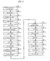
- FIG. 6is a flow diagram illustrating process steps, according to the disclosure.
- FIGS. 7A-7Rare cross-sectional diagrams illustrating an embodiment of NROM cells being fabricated according to the process steps of FIG. 6 , according to the disclosure.
- a NVM cellsuch as the NROM cell comprises two diffusions (which may be buried bitlines in a virtual ground array), a channel defined between the two diffusions, and an ONO (oxide-nitride-oxide) stack disposed above the channel.
- the nitride layer in the ONO stackis capable of storing electrical charges (such as electrons) in two distinct bit storage areas, generally referred to as the “left” bit storage area 321 and the “right” bit storage area 323 . Each of these two storage areas is generally above the one of the two diffusion areas. Due to the physical/electrical properties of the nitride material in the ONO stack (it is a “charge trapping” material, rather than a conductor), charges will generally stay where they are put (initially located).
- an “injection mechanism”is to cause electrons to be injected, into the charge storage areas of the NROM cell, and controlled so that when electrons are being injected into a given one of the charge storage areas, the electrons are injected into the charge storage area close to the diffusion, and as few as possible electrons are injected far from the junction.
- Channel hot electron (CHE) injection of electronscan be fairly well controlled to minimize far-from-junction injection.
- SIEsecondary injection of electrons
- SIEsecondary injection of electrons
- one solution to the problem of far-from-junctionis to separate the nitride layer of the ONO stack into two strips, separated by (for example) oxide (an insulating material), so that there is no charge-trapping material “far from the junction”, and in this manner, problems such as second bit effect and RAC can be minimized or avoided.
- far from the junctionmeans partway across the ONO stack to the other bit storage area.
- FIG. 5Ashows three ONO-based NVM cells (Cell A, Cell B and Cell C), each having its own ONO stack (ONO-A, ONO-B and ONO-C). The sharing of a diffusion (n+) by two adjacent cells is also illustrated in this figure.
- the process of making an ONO-based NVM cellstarts by laying down the ONO layers, then etching away portions of the top oxide and nitride (often the bottom oxide is left in place, to protect underlying silicon), resulting in a plurality (N) of ONO stacks separated from one another (although the bottom oxide may be continuous across all of the ONO stacks).
- Nthe width of a given ONO stack may be 13 nm, and the space between adjacent ONO stacks may be 12 nm.
- FIG. 5Billustrates a simplistic approach to forming two nitride strips per memory cell.
- each ONO stackis etched, at least through the top oxide and nitride (the bottom oxide may be left in place, or the nitride is etched before the top oxide is applied, resulting in two separate pieces (strips) of nitride per ONO stack, where there used to be one continuous nitride layer ( FIG. 5A ).
- ONO-AFIG. 5A
- ONO-BFIG. 5A
- ONO-Bhas been split into ONO B- 1 and B- 2 ( FIG. 5B ).
- ONO-C( FIG. 5A ) has been split into ONO C- 1 and C- 2 ( FIG. 5B ). There remains the one-to-one correspondence between ONO stacks (such as stack A) and memory cells (such as cell A). In other words, a given ONO stack becomes a given memory cell, in both FIG. 5A and FIG. 5B .
- nitride stripsa different, less difficult, more effective technique is used to create nitride strips.
- the broad purposeis the same as others—namely, having two physically separated charge storage regions in each memory cell.
- the technique of this disclosureafter the ONO stacks (such as A, B, C) are formed, they are split into two separate strips.
- FIG. 5Cillustrates that ONO stack A has been split into two “halves” (these halves are not each 50% of the stack, they may be less or more than 30% of the stack)—half stack A-L (left half of stack A) and half stack A-R (right half of stack A).
- ONO stack Bhas been split into two “halves” (these halves are not each 50% of the stack, they may be less or more than 30% of the stack)—half stack B-L (left half of stack B) and half stack B-R (right half of stack B).
- ONO stack Chas been split into two “halves” (these halves are not each 50% of the stack, they may be less or more than 30% of the stack)—half stack C-L (left half of stack C) and half stack C-R (right half of stack C).
- a gate (GATE D)is formed atop a right half (such as A-R) of one ONO stack (such as A), and the left half (such as B-L) of an adjacent ONO stack (such as B), thereby forming a cell D.
- a gate (GATE E)is formed atop a right half (such as B-R) of one ONO stack (such as B), and the left half (such as C-L) of an adjacent ONO stack (such as C), thereby forming a cell E.
- FIG. 6is a flow chart illustrating a process flow for forming NROM cells with nitride strips.
- FIGS. 7A-7Rare cross-sectional views of NROM cells with nitride strips being formed, and correlate to the process flow of FIG. 6 .
- FIG. 7Ashows a semiconductor substrate 702 which has been processed to form a starting structure having a memory array portion 704 (to the right of the figure, as viewed) and a periphery (CMOS logic) portion 706 (to the left of the figure, as viewed).
- CMOS logicperiphery
- the CMOS logic portion 706comprises N Wells and P Wells, separated by STI (shallow trench isolation) oxide, and covered by LV (low voltage) oxide and HV (high voltage) oxide.
- An STI oxide 708separates (is at the intersection of) the periphery portion 706 and the array portion 704 , and isolates the two portions from one another.
- a conventional ONO layer 720is formed on the array portion, and may comprise:
- the ONO layer 720may be annealed, using a conventional thermal anneal process.
- a layer of poly 728is disposed over the ONO layer, and a layer of oxide 730 is disposed over the poly layer 728 .
- the oxide layer 730acts as an etch stop for a subsequent poly etch and as a barrier to the subsequent hot phosphoric strip. Its thickness is adjusted accordingly.
- the poly layer 728acts a barrier to a subsequent wet oxide liner strip. Its thickness is determined by the oxide undercut and barrier effectiveness.
- the poly layer 728 and the oxide layer 730may be formed immediately after ONO anneal. The poly and oxide form a poly/oxide (PO) cap on the ONO layer.
- a layer of polysilicon (Poly-1) 732is deposited, using a conventional poly deposition process, to a initial thickness of approximately 90 nm. See FIG. 7B .
- the Poly-1 layer 732is planarized, using a conventional CMP process, resulting in a loss of approximately 5 nm of thickness (resulting poly thickness, ⁇ 85 nm).
- the Poly-1 layer 732will lose another approximately 14 nm of thickness (resulting poly thickness, ⁇ 71 nm).
- the loss of 14 nm of poly thicknesscomes from 10 nm (thin poly on ONO ??)+4 nm (10% overetch).
- the Poly-1 layer 732will lose another approximately 3 nm of thickness (resulting poly thickness, ⁇ 68 nm).
- the Poly-1 layer 732will lose another approximately 10 nm of thickness (resulting poly thickness, ⁇ 58 nm).
- the resulting approximately 55 ( ⁇ 58) nm of thickness for the Poly-1 layer 732should be sufficient for attaining an ample BL oxide thickness so as to maintain good BL oxide integrity, but not so much as to jeopardize the integrity of the narrow poly lines, and may be in the range of 40-70 nm.
- a periphery protect mask 734such as of photoresist (PR) is applied atop the poly layer and is positioned so that in a subsequent etch step the Poly-1 layer 732 will be opened (removed from) atop the array area 704 , as well as at the STI area 708 at the interface of the array area 704 and the CMOS area 706 .
- PRphotoresist
- the Poly-1 layer 732is then etched, using a conventional plasma etching process, stopping on the top oxide 730 of the PO layer resulting in a structure as shown in FIG. 7C .
- the periphery mask 734(of resist) is removed, using a conventional resist removal process, leaving the original approximately 90 nm of poly atop the periphery area 706 .
- the entire array area 704is exposed (no poly remaining), as well as the STI oxide structure 728 at the interface of the periphery area 706 and the array area 704 .
- nitride CMthe nitride hard mask layer 736 is planarized (now labeled 736 ′ (prime)) using a CMP process, leaving approximately 30 nm of nitride over the Poly-1 layer 732 .
- the resulting structureis shown in FIG. 5E .
- a step 612(“CELL Formation, OPON Etch”), the nitride hard mask layer 736 ′ is opened, in the array area 704 , using a conventional plasma etch process.
- the oxide 730 , poly 728 , top oxide 726 and nitride 724 layers (OPON)are also etched, using a conventional plasma etch process, stopping on the bottom oxide 722 (O), leaving about 2 nm of bottom oxide 722 on the surface of the substrate 702 .
- the resulting structureis shown in FIG. 7F .
- Openings 738are shown extend to the bottom oxide 722 , and have a width “F” of approximately 50 nm.
- the opening of the nitride layer 736 ′may be done with an inverse BL mask, which opens the cell area for channel formation.
- the width (Ld) of a vertical structure 740is approximately 90 nm.
- the center-to-center distance LD between vertical structuresis approximately 90 nm.
- LD2 Ld ( ONO )+ F ( BL space)
- Ld ( ONO )20 nm ONO strips (discussed hereinbelow)
- a step 614(“Cell Gate Oxide”), the bottom oxide 722 remaining after the previous etch step is cleaned (removed) if necessary, and a new oxide 742 is deposited and densified, using conventional gate oxide process, to a thickness of approximately 10 nm. (This reduces the effective size of the openings in the nitride mask.)
- the resulting structureis shown in FIG. 7G .
- the oxide 742covers everything, including the exposed surface of the substrate in the openings 738 between the vertical structures 740 , the sidewalls of the vertical structures 740 and the surface of the nitride hard mask 736 ′ in the periphery area 706 .
- step 616Poly Deposition and Fill
- Polysilicon (Poly-2) 744is deposited, using a conventional poly deposition process.
- the resulting structureis shown in FIG. 7H .
- Sufficient poly 744needs to be deposited so that the BL openings 738 are overfilled for subsequent CMP.
- the Poly-2 744is planarized, using a conventional CMP process.
- the resulting structureis shown in FIG. 7I .
- the planarized Poly-2is labeled 744 ′ (prime).
- nitride 736 ′′is removed, using a conventional Wet Nitride Strip process.
- FIG. 7JThe resulting structure is shown in FIG. 7J .
- the Poly-2 structures 744 ′have a width of approximately 30 nm. They sit atop 10 nm of “new” oxide 742 ′ and their sidewalls are covered with 10 nm of oxide 742 ′ as described hereinabove (see step 614 , FIG. 7G ).
- the Poly-2 structures 744 ′(including sidewall liner oxide 742 ′) are spaced approximately 90 nm apart from one another. (From sidewall liner oxide 742 ′ of one Poly-2 structure 744 ′ to the sidewall liner oxide 742 ′ of an adjacent Poly-2 structure 744 ′, is 90 nm.)
- step 622the sidewall liner oxide 742 ′ is stripped from the Poly-2 structures 744 ′, using a conventional wet oxide etch process.
- the resulting structureis shown in FIG. 7K .
- the resulting Poly-2 structures 744 ′are very narrow (approximately 30 nm), and the integrity of these narrow 744 ′ poly lines has to be maintained during the wet oxide strip.
- These narrow poly lines 744 ′are now relabeled 750 , and are now referred to as “poly lines”. The poly lines will eventually serve as the gates for NROM cells.
- the endmost ONO stacksare only partially used.
- spacing in this regionis determined by fanout considerations, which means ensuring that there is sufficient space to make connections between array word and bit lines and the neighboring CMOS logic.
- poly liner 752atop Poly-2 732 ′, on a side of Poly-2 732 ′, atop STI 708 , atop the poly 728 atop the ONO 720 , atop the poly lines 750 , as well as on the sides of the poly lines 750 .
- step 626(“BL Formation—Poly Liner Etchback”), poly liner 752 is etched, using a conventional isotropic process such as plasma etch, removing poly from on top of other structures, while leaving it on the sides of other structures.
- the resulting structureis shown in FIG. 7M .
- the etch processremoves the poly 728 , stopping on top oxide 726 of the ONO stack 720 .
- any poly underlying poly liner 752will be etched.
- the poly 728is removed, stopping on oxide 726 .
- the poly liner 752is now labeled 752 ′ (prime).
- the underlying Poly-2 732 ′had a thickness of approximately 85 nm, and now has a thickness of approximately 71 nm, and is labeled 732 ′′ (double prime).
- the space between poly lines 750 ′/ 752 ′is “F” (the minimum litho feature size), which is approximately 50 nm, which is the original 110 nm less two times the thickness (30 nm) of the poly liner deposition.
- the poly (P) 728 over ONObecomes removed.
- a central portion of the top oxide layer 726 of the ONO stack 720is now exposed.
- the outer edges of the ONO stackare covered by remnants (vestiges) of the original poly 728 (now labeled 728 ′), and sidewall liner poly 752 ′. (All but a portion of the layer 728 of sacrificial poly is removed.)
- the original ONO stack 720has a width of approximately 90 nm. Now, only approximately 50 nm (“F”) of the ONO stack 720 is exposed, in the space between adjacent poly liners 752 ′.
- the poly-2 732 in periphery area 706becomes thinned approximately 14 nm (it was approximately 85 nm, thick, and is now approximately 71 nm thick), and is labeled 732 ′′ (double prime).
- the STI oxide 708 at the interfaceis partially covered (by poly 752 ′).
- FIG. 7MWhat can be observed in FIG. 7M are essentially complete NROM cells (but lacking the bitline diffusions, described hereinbelow). Each cell has a two nitride strips from what was originally two distinct, adjacent ONO stacks 720 , covered by a wide conductive structure comprising a poly line ( 750 ′) plus poly liner ( 752 ′), which will function as the gate of the NROM cell as well as serving as a wordline in an array. Bitline diffusions will be performed in the “F” spaces (bitline openings 754 ) between adjacent poly structures 750 ′/ 752 ′.
- a step 628(“BL Formation—ONO Etch”), the exposed central portion of the ONO stack 720 is etched, etching away top oxide 726 and the nitride 724 , and stopping on the bottom oxide 722 , using a conventional dry etch processes.
- the bottom oxide 722is left in place to protect the underlying silicon
- the resulting structureis shown in FIG. 7N .
- the Poly-2 732 ′′may also become thinned, by about 2 nm (now shown as having a thickness of 69 nm rather than 71 nm), as a result of the previous oxide and nitride etches.
- bitlineswill be formed under the bitline openings 754 , by implanting through the remaining bottom oxide 722 .
- the 754 opening size Fis small (approximately 50 nm), reduced from its original size of 110 nm, as a result of 30 nm thick sidewall spacers 752 ′ on the poly lines 750 ′.
- this step 628performs the important function of taking one continuous ONO layer and separating it into two strips (or stripes).
- a ONO strip from one stack and a ONO strip from an adjacent stackfunction as two physically separated (yet coplanar) charge storage areas in a given NROM cell, avoiding problems associated with far-from-junction injection.
- a layer (liner) 760 of oxidehaving a thickness of approximately 10 nm, is deposited, using a conventional oxide deposition process.
- the resulting structureis shown in FIG. 7O .
- a step 632(“BL Formation—Spacer Etch”), the horizontal portions of the oxide liner 760 are etched, using a conventional plasma dry etching process. Remaining are the vertical portions of the oxide liner 760 , forming sidewall spacers 762 on the poly elements 752 ′. The resulting structure is shown in FIG. 7P .
- the thin bottom oxide on the substrate in the BL opening 754becomes removed, so it is re-created by re-oxidation, using a conventional oxidation process, and is now labeled 764 .
- the purpose of this thin (2-5 nm) layer of oxideis primarily to prevent channeling of the implanted species. (The purpose of the original bottom oxide layer 722 , when it is under nitride in an NROM cell, is to insulate the nitride from the FET channel in the underlying silicon.)
- bitline opening 754 ′(prime) is now approximately 30 nm (the original 50 nm less to 10 nm sidewall spacer thicknesses).
- bitline (BL) diffusions 764are implanted, through the bitline openings 754 ′, using a conventional implant process.
- the resulting structureis shown in FIG. 7Q . (Although a BL diffusion is shown next to the STI 708 , this BL implant serves no useful purpose, since it is not associated with an NROM cell.)
- the Arsenic (bit line) and Indium (pocket, if necessary) implantsshould be low KeV implants.
- a suitable material and dosage for BL implantis 2 ⁇ 10 15 cm 2 , 20 KeV, Arsenic. Note that there is no hard mask. Hence, a pocket implant (if necessary) should be low KeV Indium.
- the BL implantneeds to be at low energy so as not to penetrate through the reduced ( ⁇ 68 nm) poly 732 ′′. Else, the poly height could be increased to allow for an increase in KeV.
- the process parametersare targeted to achieve approximately a 5 nm overlap (OL) of BL under the edge of the ONO stack.
- FIG. 7Rshows two substantially complete NROM cells, formed from three ONO stacks, each ONO stack contributing one of two nitride stripes to a given NROM cell, complete with exemplary buried bitline diffusions functioning as source or drain (depending on the operation being performed on the NROM cell), with poly gates.
- oxide 766is deposited to fill (overfill) the bitline openings 754 ′ using conventional oxide deposition process. Then, excess oxide is removed, using a conventional CMP process. The resulting structure is shown in FIG. 5R .
- the polyshould be planarized to the point where the spacer walls 762 are vertical from the top down.
- FIGS. 7A-7R(18 figures) correspond to pages 3-20 (18 pages) of the provisional patent application from which this application claims priority. Pages 21-22 relate to wordline formation and, as stated at the last page (page 23) of the provisional, “The Remaining DDNS flow is the same as the standard DDNROM flow”.
- step 438In a step 438 (“WL Formation”), conventional steps are performed to form wordlines.
- a step 440(“Remaining Flow”), conventional steps are performed to connect the cells in the array area 704 to control circuitry in the CMOS area 706 , including fanout, as described hereinabove.
- word line sets formed as part of different process stepsmay be of slightly differing widths.
Landscapes
- Non-Volatile Memory (AREA)
- Semiconductor Memories (AREA)
Abstract
Description
- the bottom oxide layer322 may be from 3 to 6 nm, for example 4 nm thick;
- the middle nitride layer324 may be from 3 to 8 nm, for example 4 nm thick; and
- the
top oxide layer 326 may be from 5 to 15 nm, for example 10 nm thick.
- U.S. Pat. No. 6,429,063 (filed Mar. 6, 2000), entitled NROM Cell With Generally Decoupled Primary and Secondary Injection (hereinafter referred to as the '063 patent), and
- U.S. Pat. No. 6,583,007 (filed Dec. 20, 2001), entitled Reducing Secondary Injection Effects (hereinafter referred to as the '007 patent).
- anisotropic literally, one directional. An example of an anisotropic process is sunbathing. Only surfaces of the body exposed to the sun become tanned. (see “isotropic”).
- bit The word “bit” is a shortening of the words “binary digit.” A bit refers to a digit in the binary numeral system (base 2). A given bit is either a binary “1” or “0”. For example, the number 1001011 is 7 bits long. The unit is sometimes abbreviated to “b”. Terms for large quantities of bits can be formed using the standard range of prefixes, such as kilobit (Kbit), megabit (Mbit) and gigabit (Gbit). A typical unit of 8 bits is called a Byte, and the basic unit for 128 Bytes to 16K Bytes is treated as a “page”. That is the “mathematical” definition of “bit”. In some cases, the actual (physical) left and right charge storage areas of a NROM cell are conveniently referred to as the left “bit” and the right “bit”, even though they may store more than one binary bit (with MLC, each storage area can store at least two binary bits). The intended meaning of “bit” (mathematical or physical) should be apparent from the context in which it is used.
- bit line or bitline (BL). A conductor connected to (or which may actually be) the drain (or source) of a memory cell transistor.
- byte A byte is commonly used as a unit of storage measurement in computers, regardless of the type of data being stored. It is also one of the basic integral data types in many programming languages. A byte is a contiguous sequence of a fixed number of binary bits. In recent years, the use of a byte to mean 8 bits is nearly ubiquitous. The unit is sometimes abbreviated to “B”. Terms for large quantities of Bytes can be formed using the standard range of prefixes, e.g., kilobyte (KB), megabyte (MB) and gigabyte (GB).
- cap a term used to describe layers of a material disposed over another, dissimilar material, typically to protect the underlying material from damage during subsequent processing steps. A cap may be left in place, or removed, depending upon the situation.
- Cell Well (CW) the cell well is an area in the silicon substrate that is prepared for functioning as a transistor or memory cell device by doping with an electron acceptor material such as boron or indium (p, electron acceptors or holes) or with an electron donor material such as phosphorous or arsenic (n, electron donors). The depth of a cell well is defined by the depth of the dopant distribution.
- CHEI short for channel hot electron injection. sometimes abbreviated “CHE”.
- CHISEL short for channel initiated secondary electron.
- CMOS short for complementary metal oxide semiconductor. CMOS consists of n-channel and p-channel MOS transistors. Due to very low power consumption and dissipation as well minimization of the current in “off” state CMOS is a very effective device configuration for implementation of digital functions. CMOS is a key device in state-of-the-art silicon microelectronics.
- CMOS Inverter: A pair of two complementary transistors (a p-channel and an n-channel) with the source of the n-channel transistor connected to the drain of the p-channel one and the gates connected to each other. The output (drain of the p-channel transistor) is high whenever the input (gate) is low and the other way round. The CMOS inverter is the basic building block of CMOS digital circuits.
- NMOS: n-channel CMOS.
- PMOS: p-channel CMOS.
- CMP short for chemical-mechanical polishing. CMP is a process, using both chemicals and abrasives, comparable to lapping, for removing material from a built up structure, resulting in a particularly planar resulting structure.
- Dopant element introduced into semiconductor to establish either p-type (acceptors) or n-type (donors) conductivity; common dopants in silicon: p-type, boron, B, Indium, In; n-type phosphorous, P, arsenic, As, antimony, Sb.
- EEPROM short for electrically erasable, programmable read only memory. EEPROMs have the advantage of being able to selectively erase any part of the chip without the need to erase the entire chip and without the need to remove the chip from the circuit. The minimum erase unit is 1 Byte and more typically a full Page. While an erase and rewrite of a location appears nearly instantaneous to the user, the write process is usually slightly slower than the read process; the chip can usually be read at full system speeds.
- EPROM short for erasable, programmable read only memory. EPROM is a memory cell in which information (data) can be erased and replaced with new information (data).
- Erase a method to erase data on a large set of bits in the array, by applying voltage scheme that inject holes or remove electrons in the bit set. This method causes all bits to reach a low Vt level.
- FET short for field effect transistor. The FET is a transistor that relies on an electric field to control the shape and hence the conductivity of a “channel” in a semiconductor material. FETs are sometimes used as voltage-controlled resistors. The terminals of FETs are called gate, drain and source.
- Flash memory Flash memory is a form of non-volatile memory (EEPROM) that can be electrically erased and reprogrammed. Flash memory architecture allows multiple memory locations to be erased or written in one programming operation.
- FN tunneling Field emission—also called Fowler-Nordheim tunneling—is the process whereby electrons tunnel through a barrier in the presence of a high electric field. This quantum mechanical tunneling process is an important mechanism for thin barriers as those in metal-semiconductor junctions on highly-doped semiconductors. Using FN tunneling, electrons can be moved to the floating gate of a MOSFET memory cell.
- half cell this term is sometimes used to refer to the two distinct charge storage areas (left and right bits) of an NROM memory cell.
- HHI short for hot hole injection
- isotropic literally, identical in all directions. An example of an isotropic process is dissolving a tablet in water. All exposed surfaces of the tablet are uniformly acted upon. (see “anisotropic”)
- mask a layer of material which is applied over an underlying layer of material, and patterned to have openings, so that the underlying layer can be processed where there are openings. After processing the underlying layer, the mask may be removed. Common masking materials are photoresist and nitride. Nitride is usually considered to be a “hard mask”.
- MLC short for multi-level cell. In the context of a floating gate (FG) memory cell, MLC means that at least two bits of information can be stored in the memory cell. In the context of an NROM memory cell, MLC means that at least four bits of information can be stored in the memory cell—at least two bits in each of the two charge storage areas.
- MOS short for metal oxide semiconductor.
- MOSFET short for metal oxide semiconductor field-effect transistor. MOSFET is by far the most common field-effect transistor in both digital and analog circuits. The MOSFET is composed of a channel of n-type or p-type semiconductor material, and is accordingly called an NMOSFET or a PMOSFET. (The ‘metal’ in the name is an anachronism from early chips where gates were metal; modern chips use polysilicon gates, but are still called MOSFETs).
- nitride commonly used to refer to silicon nitride (chemical formula Si3N4). A dielectric material commonly used in integrated circuit manufacturing. Forms an excellent mask (barrier) against oxidation of silicon (Si). Nitride is commonly used as a hard mask or, in the case of a NVM memory cell having an ONO layer as a charge-trapping material.
- n-type semiconductor in which concentration of electrons is higher than the concentration of “holes”. See p-type.
- NROM short for nitride read only memory.
- NVM short for non-volatile memory. NVM is computer memory that can retain the stored information even when not powered. Examples of non-volatile memory include read-only memory, flash memory, most types of magnetic computer storage devices (e.g. hard disks, floppy disk drives, and magnetic tape), optical disc drives, and early computer storage methods such as paper tape and punch cards. Non-volatile memory is typically used for the task of secondary storage, or long-term persistent storage. The most widely used form of primary storage today is a volatile form of random access memory (RAM), meaning that when the computer is shut down, anything contained in RAM is lost. Unfortunately most forms of non-volatile memory have limitations which make it unsuitable for use as primary storage. Typically non-volatile memory either costs more or performs worse than volatile random access memory. (By analogy, the simplest form of a NVM memory cell is a simple light switch. Indeed, such a switch can be set to one of two (binary) positions, and “memorize” that position.)
- ONO short for oxide-nitride-oxide. ONO is used as a charge storage insulator consisting of a sandwich of thermally insulating oxide, and charge-trapping nitride.
- oxide commonly used to refer to silicon dioxide (SiO2). Also known as silica. SiO2 is the most common insulator in semiconductor device technology, particularly in silicon MOS/CMOS where it is used as a gate dielectric (gate oxide); high quality films are obtained by thermal oxidation of silicon. Thermal SiO2 forms a smooth, low-defect interface with Si, and can be also readily deposited by CVD. Some particular applications of oxide are:
- LV Oxide short for low voltage oxide. LV refers to the process used to deposit the oxide.
- HV Oxide short for high voltage oxide. HV refers to the process used to deposit the oxide
- STI Oxide short for shallow trench oxide. Oxide-filled trenches are commonly used to separate one region (or device) of a semiconductor substrate from another region (or device).
- Poly short for polycrystalline silicon (Si). Heavily doped poly Si is commonly used as a gate contact in silicon MOS and CMOS devices;
- p-type semiconductor in which concentration of “holes” is higher than the concentration of electrons. See n-type. Examples of p-type silicon include silicon doped (enhanced) with boron (B), Indium (In) and the like.
- Program a method to program a memory cells, or half cells, typically by applying a voltage scheme that injects electrons to increase the Vt of the cells or half cells being programmed.
- PROM short for programmable read-only memory.
- RAM short for random access memory. RAM refers to data storage formats and equipment that allow the stored data to be accessed in any order—that is, at random, not just in sequence. In contrast, other types of memory devices (such as magnetic tapes, disks, and drums) can access data on the storage medium only in a predetermined order due to constraints in their mechanical design.
- Read a method to read the digital data stored in a memory cell.
- resist short for photoresist. also abbreviated “PR”. Photoresist is often used as a masking material in photolithographic processes to reproduce either a positive or a negative image on a structure, prior to etching (removal of material which is not masked). PR is usually washed off after having served its purpose as a masking material.
- ROM short for read-only memory.
- SEI short for secondary electron injection (or simply “secondary injection”). SEI occurs as a result of impact ionization by CHE electrons (e1) near the drain diffusion, generating an electron-hole pair (e2-h2), the hole (h2) of which continues into the substrate whereat another impact ionization results in another electron-hole pair (e3-h3), and the e3 electron becomes injected into the charge storage area(s) of the memory cell.
- Si Silicon, a semiconductor.
- SLC short for single level cell. In the context of a floating gate (FG) memory cell, SLC means that one bit of information can be stored in the memory cell. In the context of an NROM memory cell, SLC means that at least two bits of information can be stored in the memory cell.
- SONOS Si-Oxide-Nitride-Oxide-Si, another way to describe ONO with the Si underneath and the Poly gate on top.
- spacer a spacer, as the name implies, is a material (such as a layer of oxide) disposed on an element (such as a poly gate electrode). For example, sidewall spacers disposed on sides of a gate electrode cause subsequent implants to occur further away from the gate than otherwise (without the spacers in place).
- STI short for shallow trench isolation
- TEHH short for Tunnel Enhanced Hot Hole injection. TEHH is an “injection mechanism”.
- Units of Length Various units of length may be used herein, as follows:
- meter (m) A meter is the SI unit of length, slightly longer than a yard. 1 meter=˜39 inches. 1 kilometer (km)=1000 meters=˜0.6 miles. 1,000,000 microns=1 meter. 1,000 millimeters (mm)=1 meter. 100 centimeters (cm)=1 meter.
- micron (μm) one millionth of a meter (0.000001 meter); also referred to as a micrometer.
mil 1/1000 or 0.001 of an inch; 1 mil=25.4 microns.- nanometer (nm) one billionth of a meter (0.000000001 meter).
- Angstrom (Å) one tenth of a billionth of a meter. 10 Å=1 nm.
- Voltage abbreviated v, or V. A voltage can be positive or negative (or zero). Usually, a negative voltage is preceeded by a minus sign (−). Sometimes a positive voltage is preceeded by a plus sign (+), or no sign at all. A number of voltages are relevant with regard to operating a memory cell, and are typically designated by the capital letter “V”, followed by another letter or letters. Some exemplary voltages of interest are:
- KeV short for kilo (thousand) electron volts
- Vt short for threshold voltage
- Vs short for source voltage
- Vd short for drain voltage
- Vg short for gate voltage
- Vbl short for bitline voltage. (the bitline may function as source or drain)
- Vwl short for wordline voltage (which typically is the same as Vg)
- word line or wordline, (WL). A conductor normally connected to the gate of a memory cell transistor. The wordline may actually be the gate electrode of the memory cell.
- write a combined method of first erase a large set of bits, then program a new data into the bit set.
- BB short for buried bitline.
- DDNROM short for double density NROM
- DDNS short for double density nitride strips
- DNW short for deep N-well.
- DPP short for dual poly process.
- F short for feature size, which is the minimum size of an element.
- HM short for hard mask.
- HV OX or HV_OX. short for high voltage oxide.
- HV short for high voltage
- IMP short for implant.
- LV short for low voltage
- MV OX short for medium voltage oxide.
- OL short for overlap.
- PHOTO short for photoresist or photomask, depending on the context.
- PI short for pocket implant.
- PO short for poly/oxide.
- poly short for polysilicon.
- PRECLN short for pre-clean.
- PRRM short for photoresist removal
- PT short for punchthrough.
- PWI short for p-well implant
- OPON short for oxide-polysilicon-oxide-nitride
- a bottom oxide layer722 (compare322), for example 4 nm thick;
- a middle nitride layer724 (compare324), for example 4 nm thick; and
- a top oxide layer726 (compare326), for example 10 nm thick.
LD=2Ld(ONO)+F(BLspace)
Ld(ONO)=20 nmONOstrips (discussed hereinbelow)
Claims (3)
Priority Applications (1)
| Application Number | Priority Date | Filing Date | Title |
|---|---|---|---|
| US11/646,430US7638835B2 (en) | 2006-02-28 | 2006-12-28 | Double density NROM with nitride strips (DDNS) |
Applications Claiming Priority (3)
| Application Number | Priority Date | Filing Date | Title |
|---|---|---|---|
| US77711406P | 2006-02-28 | 2006-02-28 | |
| US11/489,237US7804126B2 (en) | 2005-07-18 | 2006-07-18 | Dense non-volatile memory array and method of fabrication |
| US11/646,430US7638835B2 (en) | 2006-02-28 | 2006-12-28 | Double density NROM with nitride strips (DDNS) |
Related Parent Applications (2)
| Application Number | Title | Priority Date | Filing Date |
|---|---|---|---|
| US11/489,237Continuation-In-PartUS7804126B2 (en) | 2005-07-18 | 2006-07-18 | Dense non-volatile memory array and method of fabrication |
| US11489327Continuation-In-Part | 2006-07-19 |
Publications (2)
| Publication Number | Publication Date |
|---|---|
| US20070200180A1 US20070200180A1 (en) | 2007-08-30 |
| US7638835B2true US7638835B2 (en) | 2009-12-29 |
Family
ID=38443159
Family Applications (1)
| Application Number | Title | Priority Date | Filing Date |
|---|---|---|---|
| US11/646,430Expired - Fee RelatedUS7638835B2 (en) | 2006-02-28 | 2006-12-28 | Double density NROM with nitride strips (DDNS) |
Country Status (1)
| Country | Link |
|---|---|
| US (1) | US7638835B2 (en) |
Cited By (6)
| Publication number | Priority date | Publication date | Assignee | Title |
|---|---|---|---|---|
| US20100109070A1 (en)* | 2008-11-06 | 2010-05-06 | Spansion Llc | Fabricating method of mirror bit memory device having split ono film with top oxide film formed by oxidation process |
| US20110278660A1 (en)* | 2007-08-08 | 2011-11-17 | Spansion Llc | Oro and orpro with bit line trench to suppress transport program disturb |
| US20120001233A1 (en)* | 2010-07-01 | 2012-01-05 | Aplus Flash Technology, Inc. | Novel embedded NOR flash memory process with NAND cell and true logic compatible low voltage device |
| US8471328B2 (en) | 2010-07-26 | 2013-06-25 | United Microelectronics Corp. | Non-volatile memory and manufacturing method thereof |
| US9673207B2 (en)* | 2015-08-20 | 2017-06-06 | Sandisk Technologies Llc | Shallow trench isolation trenches and methods for NAND memory |
| US11257833B2 (en)* | 2019-02-26 | 2022-02-22 | Winbond Electronics Corp. | Memory device and manufacturing method thereof |
Families Citing this family (6)
| Publication number | Priority date | Publication date | Assignee | Title |
|---|---|---|---|---|
| US7919368B2 (en) | 2009-05-29 | 2011-04-05 | Texas Instruments Incorporated | Area-efficient electrically erasable programmable memory cell |
| US8848454B2 (en)* | 2012-10-02 | 2014-09-30 | United Microelectronics Corp. | Method for programming non-volatile memory cell, non-volatile memory array and non-volatile memory apparatus |
| CN104058363B (en)* | 2013-03-22 | 2016-01-20 | 上海丽恒光微电子科技有限公司 | Based on the display unit and forming method thereof of MEMS transmissive light valve |
| CN107580728A (en)* | 2015-03-26 | 2018-01-12 | Neo半导体公司 | 3D dual density NAND quick-flash memories |
| US9754788B2 (en)* | 2015-07-13 | 2017-09-05 | United Microelectronics Corp. | Manufacturing method of semiconductor structure including planarizing a polysilicon layer over an array area and a periphery area |
| US10629499B2 (en) | 2018-06-13 | 2020-04-21 | International Business Machines Corporation | Method and structure for forming a vertical field-effect transistor using a replacement metal gate process |
Citations (627)
| Publication number | Priority date | Publication date | Assignee | Title |
|---|---|---|---|---|
| GB1297899A (en) | 1970-10-02 | 1972-11-29 | ||
| US3881180A (en) | 1971-11-30 | 1975-04-29 | Texas Instruments Inc | Non-volatile memory cell |
| US3895360A (en) | 1974-01-29 | 1975-07-15 | Westinghouse Electric Corp | Block oriented random access memory |
| US3952325A (en) | 1971-07-28 | 1976-04-20 | U.S. Philips Corporation | Semiconductor memory elements |
| US4016588A (en) | 1974-12-27 | 1977-04-05 | Nippon Electric Company, Ltd. | Non-volatile semiconductor memory device |
| US4017888A (en) | 1975-12-31 | 1977-04-12 | International Business Machines Corporation | Non-volatile metal nitride oxide semiconductor device |
| US4145703A (en) | 1977-04-15 | 1979-03-20 | Supertex, Inc. | High power MOS device and fabrication method therefor |
| JPS5453929U (en) | 1977-09-21 | 1979-04-14 | ||
| US4151021A (en) | 1977-01-26 | 1979-04-24 | Texas Instruments Incorporated | Method of making a high density floating gate electrically programmable ROM |
| JPS54125938U (en) | 1978-02-22 | 1979-09-03 | ||
| US4173766A (en) | 1977-09-16 | 1979-11-06 | Fairchild Camera And Instrument Corporation | Insulated gate field-effect transistor read-only memory cell |
| US4173791A (en) | 1977-09-16 | 1979-11-06 | Fairchild Camera And Instrument Corporation | Insulated gate field-effect transistor read-only memory array |
| US4247861A (en) | 1979-03-09 | 1981-01-27 | Rca Corporation | High performance electrically alterable read-only memory (EAROM) |
| WO1981000790A1 (en) | 1979-09-13 | 1981-03-19 | Ncr Co | Silicon gate non-volatile memory device |
| US4257832A (en) | 1978-07-24 | 1981-03-24 | Siemens Aktiengesellschaft | Process for producing an integrated multi-layer insulator memory cell |
| US4281397A (en) | 1979-10-29 | 1981-07-28 | Texas Instruments Incorporated | Virtual ground MOS EPROM or ROM matrix |
| US4306353A (en) | 1979-06-13 | 1981-12-22 | Siemens Aktiengesellschaft | Process for production of integrated MOS circuits with and without MNOS memory transistors in silicon-gate technology |
| US4342102A (en) | 1980-06-18 | 1982-07-27 | Signetics Corporation | Semiconductor memory array |
| US4342149A (en) | 1979-11-23 | 1982-08-03 | Siemens Aktiengesellschaft | Method of making very short channel length MNOS and MOS devices by double implantation of one conductivity type subsequent to other type implantation |
| US4360900A (en) | 1978-11-27 | 1982-11-23 | Texas Instruments Incorporated | Non-volatile semiconductor memory elements |
| US4373248A (en) | 1978-07-12 | 1983-02-15 | Texas Instruments Incorporated | Method of making high density semiconductor device such as floating gate electrically programmable ROM or the like |
| US4380057A (en) | 1980-10-27 | 1983-04-12 | International Business Machines Corporation | Electrically alterable double dense memory |
| US4388705A (en) | 1981-10-01 | 1983-06-14 | Mostek Corporation | Semiconductor memory circuit |
| US4389705A (en) | 1981-08-21 | 1983-06-21 | Mostek Corporation | Semiconductor memory circuit with depletion data transfer transistor |
| US4404747A (en) | 1981-07-29 | 1983-09-20 | Schur, Inc. | Knife and sheath assembly |
| US4435786A (en) | 1981-11-23 | 1984-03-06 | Fairchild Camera And Instrument Corporation | Self-refreshing memory cell |
| US4448400A (en) | 1981-07-13 | 1984-05-15 | Eliyahou Harari | Highly scalable dynamic RAM cell with self-signal amplification |
| US4471373A (en) | 1980-02-27 | 1984-09-11 | Hitachi, Ltd. | Semiconductor integrated circuit device with memory MISFETS and thin and thick gate insulator MISFETS |
| US4494016A (en) | 1982-07-26 | 1985-01-15 | Sperry Corporation | High performance MESFET transistor for VLSI implementation |
| US4507673A (en) | 1979-10-13 | 1985-03-26 | Tokyo Shibaura Denki Kabushiki Kaisha | Semiconductor memory device |
| US4521796A (en) | 1980-12-11 | 1985-06-04 | General Instrument Corporation | Memory implant profile for improved channel shielding in electrically alterable read only memory semiconductor device |
| US4527257A (en) | 1982-08-25 | 1985-07-02 | Westinghouse Electric Corp. | Common memory gate non-volatile transistor memory |
| JPS60200566A (en) | 1984-03-26 | 1985-10-11 | Hitachi Ltd | Semiconductor integrated circuit device |
| JPS60201594A (en) | 1984-03-23 | 1985-10-12 | Hitachi Micro Comput Eng Ltd | semiconductor storage device |
| GB2157489A (en) | 1984-03-23 | 1985-10-23 | Hitachi Ltd | A semiconductor integrated circuit memory device |
| US4586163A (en) | 1982-09-13 | 1986-04-29 | Toshiba Shibaura Denki Kabushiki Kaisha | Multi-bit-per-cell read only memory circuit |
| US4613956A (en) | 1983-02-23 | 1986-09-23 | Texas Instruments Incorporated | Floating gate memory with improved dielectric |
| US4630085A (en) | 1984-02-28 | 1986-12-16 | Nec Corporation | Erasable, programmable read-only memory device |
| US4663645A (en) | 1984-05-23 | 1987-05-05 | Hitachi, Ltd. | Semiconductor device of an LDD structure having a floating gate |
| US4665426A (en) | 1985-02-01 | 1987-05-12 | Advanced Micro Devices, Inc. | EPROM with ultraviolet radiation transparent silicon nitride passivation layer |
| US4667217A (en) | 1985-04-19 | 1987-05-19 | Ncr Corporation | Two bit vertically/horizontally integrated memory cell |
| US4672409A (en) | 1980-12-25 | 1987-06-09 | Fujitsu Limited | Nonvolatile semiconductor memory device |
| US4725984A (en) | 1984-02-21 | 1988-02-16 | Seeq Technology, Inc. | CMOS eprom sense amplifier |
| US4733105A (en) | 1985-09-04 | 1988-03-22 | Oki Electric Industry Co., Ltd. | CMOS output circuit |
| US4742491A (en) | 1985-09-26 | 1988-05-03 | Advanced Micro Devices, Inc. | Memory cell having hot-hole injection erase mode |
| US4758869A (en) | 1986-08-29 | 1988-07-19 | Waferscale Integration, Inc. | Nonvolatile floating gate transistor structure |
| US4760555A (en) | 1986-04-21 | 1988-07-26 | Texas Instruments Incorporated | Memory array with an array reorganizer |
| US4761764A (en) | 1985-04-18 | 1988-08-02 | Nec Corporation | Programmable read only memory operable with reduced programming power consumption |
| US4769340A (en) | 1983-11-28 | 1988-09-06 | Exel Microelectronics, Inc. | Method for making electrically programmable memory device by doping the floating gate by implant |
| JPS63249375A (en) | 1987-04-06 | 1988-10-17 | Oki Electric Ind Co Ltd | Data erasing method for semiconductor memory device |
| US4780424A (en) | 1987-09-28 | 1988-10-25 | Intel Corporation | Process for fabricating electrically alterable floating gate memory devices |
| US4839705A (en) | 1987-12-16 | 1989-06-13 | Texas Instruments Incorporated | X-cell EEPROM array |
| US4847808A (en) | 1986-04-22 | 1989-07-11 | Nec Corporation | Read only semiconductor memory having multiple bit cells |
| US4857770A (en) | 1988-02-29 | 1989-08-15 | Advanced Micro Devices, Inc. | Output buffer arrangement for reducing chip noise without speed penalty |
| US4870470A (en) | 1987-10-16 | 1989-09-26 | International Business Machines Corporation | Non-volatile memory cell having Si rich silicon nitride charge trapping layer |
| US4888735A (en) | 1987-12-30 | 1989-12-19 | Elite Semiconductor & Systems Int'l., Inc. | ROM cell and array configuration |
| US4916671A (en) | 1988-09-06 | 1990-04-10 | Mitsubishi Denki Kabushiki Kaisha | Semiconductor memory device having sense amplifier having improved activation timing thereof and operating method thereof |
| US4941028A (en) | 1988-08-10 | 1990-07-10 | Actel Corporation | Structure for protecting thin dielectrics during processing |
| US4961010A (en) | 1989-05-19 | 1990-10-02 | National Semiconductor Corporation | Output buffer for reducing switching induced noise |
| US4992391A (en) | 1989-11-29 | 1991-02-12 | Advanced Micro Devices, Inc. | Process for fabricating a control gate for a floating gate FET |
| US5021999A (en) | 1987-12-17 | 1991-06-04 | Mitsubishi Denki Kabushiki Kaisha | Non-volatile semiconductor memory device with facility of storing tri-level data |
| US5027321A (en) | 1989-11-21 | 1991-06-25 | Intel Corporation | Apparatus and method for improved reading/programming of virtual ground EPROM arrays |
| US5029063A (en) | 1989-03-25 | 1991-07-02 | Eurosil Electronic Gmbh | MOSFET multiplying circuit |
| US5042009A (en) | 1988-12-09 | 1991-08-20 | Waferscale Integration, Inc. | Method for programming a floating gate memory device |
| JPH03285358A (en) | 1990-04-02 | 1991-12-16 | Matsushita Electron Corp | Driving method for nonvolatile semiconductor storage device |
| US5075245A (en) | 1990-08-03 | 1991-12-24 | Intel Corporation | Method for improving erase characteristics of buried bit line flash EPROM devices without using sacrificial oxide growth and removal steps |
| US5081371A (en) | 1990-11-07 | 1992-01-14 | U.S. Philips Corp. | Integrated charge pump circuit with back bias voltage reduction |
| US5086325A (en) | 1990-11-21 | 1992-02-04 | Atmel Corporation | Narrow width EEPROM with single diffusion electrode formation |
| US5094968A (en) | 1990-11-21 | 1992-03-10 | Atmel Corporation | Fabricating a narrow width EEPROM with single diffusion electrode formation |
| US5104819A (en) | 1989-08-07 | 1992-04-14 | Intel Corporation | Fabrication of interpoly dielctric for EPROM-related technologies |
| US5117389A (en) | 1990-09-05 | 1992-05-26 | Macronix International Co., Ltd. | Flat-cell read-only-memory integrated circuit |
| US5120672A (en) | 1989-02-22 | 1992-06-09 | Texas Instruments Incorporated | Fabricating a single level merged EEPROM cell having an ONO memory stack substantially spaced from the source region |
| JPH04226071A (en) | 1990-05-16 | 1992-08-14 | Ricoh Co Ltd | Semiconductor memory device |
| US5142496A (en) | 1991-06-03 | 1992-08-25 | Advanced Micro Devices, Inc. | Method for measuring VT 's less than zero without applying negative voltages |
| US5142495A (en) | 1989-03-10 | 1992-08-25 | Intel Corporation | Variable load for margin mode |
| JPH04291962A (en) | 1991-03-20 | 1992-10-16 | Fujitsu Ltd | Mask ROM manufacturing method and mask ROM |
| US5159570A (en) | 1987-12-22 | 1992-10-27 | Texas Instruments Incorporated | Four memory state EEPROM |
| US5168334A (en) | 1987-07-31 | 1992-12-01 | Texas Instruments, Incorporated | Non-volatile semiconductor memory |
| US5172338A (en) | 1989-04-13 | 1992-12-15 | Sundisk Corporation | Multi-state EEprom read and write circuits and techniques |
| US5175120A (en) | 1991-10-11 | 1992-12-29 | Micron Technology, Inc. | Method of processing a semiconductor wafer to form an array of nonvolatile memory devices employing floating gate transistors and peripheral area having CMOS transistors |
| US5204835A (en) | 1990-06-13 | 1993-04-20 | Waferscale Integration Inc. | Eprom virtual ground array |
| US5214303A (en) | 1991-02-08 | 1993-05-25 | Sharp Kabushiki Kaisha | Semiconductor device ROM having an offset region |
| JPH0521758Y2 (en) | 1986-05-19 | 1993-06-03 | ||
| US5237213A (en) | 1991-04-15 | 1993-08-17 | Oki Electric Industry Co., Ltd. | Semiconductor integrated circuit with low-noise output buffers |
| US5236853A (en) | 1992-02-21 | 1993-08-17 | United Microelectronics Corporation | Self-aligned double density polysilicon lines for ROM and EPROM |
| US5241497A (en) | 1990-06-14 | 1993-08-31 | Creative Integrated Systems, Inc. | VLSI memory with increased memory access speed, increased memory cell density and decreased parasitic capacitance |
| US5260593A (en) | 1991-12-10 | 1993-11-09 | Micron Technology, Inc. | Semiconductor floating gate device having improved channel-floating gate interaction |
| US5268861A (en) | 1991-04-10 | 1993-12-07 | Sharp Kabushiki Kaisha | Semiconductor read only memory |
| JPH05326893A (en) | 1992-05-25 | 1993-12-10 | Rohm Co Ltd | Non-volatile storage device |
| US5276646A (en) | 1990-09-25 | 1994-01-04 | Samsung Electronics Co., Ltd. | High voltage generating circuit for a semiconductor memory circuit |
| US5280420A (en) | 1992-10-02 | 1994-01-18 | National Semiconductor Corporation | Charge pump which operates on a low voltage power supply |
| US5289412A (en) | 1992-06-19 | 1994-02-22 | Intel Corporation | High-speed bias-stabilized current-mirror referencing circuit for non-volatile memories |
| US5293563A (en) | 1988-12-29 | 1994-03-08 | Sharp Kabushiki Kaisha | Multi-level memory cell with increased read-out margin |
| US5295092A (en) | 1992-01-21 | 1994-03-15 | Sharp Kabushiki Kaisha | Semiconductor read only memory |
| US5295108A (en) | 1992-04-08 | 1994-03-15 | Nec Corporation | Electrically erasable and programmable read only memory device with simple controller for selecting operational sequences after confirmation |
| US5305262A (en) | 1991-09-11 | 1994-04-19 | Kawasaki Steel Corporation | Semiconductor integrated circuit |
| US5311049A (en) | 1991-10-17 | 1994-05-10 | Rohm Co., Ltd. | Non-volatile semiconductor memory with outer drain diffusion layer |
| US5315541A (en) | 1992-07-24 | 1994-05-24 | Sundisk Corporation | Segmented column memory array |
| JPH06151833A (en) | 1992-11-16 | 1994-05-31 | Mitsubishi Electric Corp | Semiconductor device and manufacturing method thereof |
| US5324675A (en) | 1992-03-31 | 1994-06-28 | Kawasaki Steel Corporation | Method of producing semiconductor devices of a MONOS type |
| US5335198A (en) | 1993-05-06 | 1994-08-02 | Advanced Micro Devices, Inc. | Flash EEPROM array with high endurance |
| US5334555A (en) | 1991-11-06 | 1994-08-02 | Sony Corporation | Method of determining conditions for plasma silicon nitride film growth and method of manufacturing semiconductor device |
| US5338954A (en) | 1991-10-31 | 1994-08-16 | Rohm Co., Ltd. | Semiconductor memory device having an insulating film and a trap film joined in a channel region |
| JPH06232416A (en) | 1993-02-03 | 1994-08-19 | Rohm Co Ltd | Semiconductor storage device and manufacture thereof |
| US5345425A (en) | 1990-11-20 | 1994-09-06 | Fujitsu Limited | Semiconductor memory device |
| US5349221A (en) | 1991-10-25 | 1994-09-20 | Rohm Co., Ltd. | Semiconductor memory device and method of reading out information for the same |
| US5350710A (en) | 1993-06-24 | 1994-09-27 | United Microelectronics Corporation | Device for preventing antenna effect on circuit |
| US5352620A (en) | 1984-05-23 | 1994-10-04 | Hitachi, Ltd. | Method of making semiconductor device with memory cells and peripheral transistors |
| US5357134A (en) | 1991-10-31 | 1994-10-18 | Rohm Co., Ltd. | Nonvolatile semiconductor device having charge trap film containing silicon crystal grains |
| US5359554A (en) | 1991-08-27 | 1994-10-25 | Matsushita Electric Industrial Co., Ltd. | Semiconductor memory device having an energy gap for high speed operation |
| US5361343A (en) | 1991-07-30 | 1994-11-01 | Intel Corporation | Microprocessor system including first and second nonvolatile memory arrays which may be simultaneously read and reprogrammed |
| US5366915A (en) | 1992-08-28 | 1994-11-22 | Nec Corporation | Process of fabricating floating gate type field effect transistor having drain region gently varied in impurity profile |
| US5369615A (en) | 1991-03-15 | 1994-11-29 | Sundisk Corporation | Method for optimum erasing of EEPROM |
| US5375094A (en) | 1992-06-19 | 1994-12-20 | Kabushiki Kaisha Toshiba | Nonvolatile semiconductor memory system with a plurality of erase blocks |
| US5381374A (en) | 1992-01-09 | 1995-01-10 | Kabushiki Kaisha Toshiba | Memory cell data output circuit having improved access time |
| US5393701A (en) | 1993-04-08 | 1995-02-28 | United Microelectronics Corporation | Layout design to eliminate process antenna effect |
| US5394355A (en) | 1990-08-28 | 1995-02-28 | Mitsubishi Denki Kabushiki Kaisha | Read only memory for storing multi-data |
| US5400286A (en) | 1993-08-17 | 1995-03-21 | Catalyst Semiconductor Corp. | Self-recovering erase scheme to enhance flash memory endurance |
| US5399891A (en) | 1992-01-22 | 1995-03-21 | Macronix International Co., Ltd. | Floating gate or flash EPROM transistor array having contactless source and drain diffusions |
| US5402374A (en) | 1993-04-30 | 1995-03-28 | Rohm Co., Ltd. | Non-volatile semiconductor memory device and memory circuit using the same |
| US5412601A (en) | 1992-08-31 | 1995-05-02 | Nippon Steel Corporation | Non-volatile semiconductor memory device capable of storing multi-value data in each memory cell |
| US5414693A (en) | 1991-08-29 | 1995-05-09 | Hyundai Electronics Industries Co., Ltd. | Self-aligned dual-bit split gate (DSG) flash EEPROM cell |
| US5418176A (en) | 1994-02-17 | 1995-05-23 | United Microelectronics Corporation | Process for producing memory devices having narrow buried N+ lines |
| US5418743A (en) | 1992-12-07 | 1995-05-23 | Nippon Steel Corporation | Method of writing into non-volatile semiconductor memory |
| US5422844A (en) | 1992-12-21 | 1995-06-06 | National Semiconductor Corporation | Memory array with field oxide islands eliminated and method |
| US5424567A (en) | 1991-05-15 | 1995-06-13 | North American Philips Corporation | Protected programmable transistor with reduced parasitic capacitances and method of fabrication |
| US5424978A (en) | 1993-03-15 | 1995-06-13 | Nippon Steel Corporation | Non-volatile semiconductor memory cell capable of storing more than two different data and method of using the same |
| US5426605A (en) | 1992-08-19 | 1995-06-20 | U.S. Philips Corporation | Semiconductor memory device |
| US5428621A (en) | 1992-09-21 | 1995-06-27 | Sundisk Corporation | Latent defect handling in EEPROM devices |
| US5434825A (en) | 1988-06-08 | 1995-07-18 | Harari; Eliyahou | Flash EEPROM system cell array with more than two storage states per memory cell |
| US5436478A (en) | 1994-03-16 | 1995-07-25 | National Semiconductor Corporation | Fast access AMG EPROM with segment select transistors which have an increased width |
| US5436481A (en) | 1993-01-21 | 1995-07-25 | Nippon Steel Corporation | MOS-type semiconductor device and method of making the same |
| JPH07193151A (en) | 1993-12-27 | 1995-07-28 | Toshiba Corp | Nonvolatile semiconductor memory device and its storage method |
| US5440505A (en) | 1994-01-21 | 1995-08-08 | Intel Corporation | Method and circuitry for storing discrete amounts of charge in a single memory element |
| US5450341A (en) | 1992-08-31 | 1995-09-12 | Nippon Steel Corporation | Non-volatile semiconductor memory device having memory cells, each for at least three different data writable thereinto selectively and a method of using the same |
| US5450354A (en) | 1992-08-31 | 1995-09-12 | Nippon Steel Corporation | Non-volatile semiconductor memory device detachable deterioration of memory cells |
| US5455793A (en) | 1992-01-15 | 1995-10-03 | National Semiconductor Corp. | Electrically reprogrammable EPROM cell with merged transistor and optimum area |
| US5467308A (en) | 1994-04-05 | 1995-11-14 | Motorola Inc. | Cross-point eeprom memory array |
| US5477499A (en) | 1993-10-13 | 1995-12-19 | Advanced Micro Devices, Inc. | Memory architecture for a three volt flash EEPROM |
| US5495440A (en) | 1993-01-19 | 1996-02-27 | Mitsubishi Denki Kabushiki Kaisha | Semiconductor memory device having hierarchical bit line structure |
| US5496753A (en) | 1992-05-29 | 1996-03-05 | Citizen Watch, Co., Ltd. | Method of fabricating a semiconductor nonvolatile storage device |
| US5508968A (en) | 1994-08-12 | 1996-04-16 | International Business Machines Corporation | Dynamic random access memory persistent page implemented as processor register sets |
| JPH08106791A (en) | 1994-10-03 | 1996-04-23 | Matsushita Electric Ind Co Ltd | Driving method for semiconductor memory device |
| US5518942A (en) | 1995-02-22 | 1996-05-21 | Alliance Semiconductor Corporation | Method of making flash EPROM cell having improved erase characteristics by using a tilt angle implant |
| WO1996015553A1 (en) | 1994-11-15 | 1996-05-23 | Advanced Micro Devices, Inc. | Transistor structure with specific gate and pad areas |
| US5521870A (en) | 1993-12-07 | 1996-05-28 | Nec Corporation | Semiconductor memory device having a coincidence detection circuit and its test method |
| US5523972A (en) | 1994-06-02 | 1996-06-04 | Intel Corporation | Method and apparatus for verifying the programming of multi-level flash EEPROM memory |
| US5523251A (en) | 1994-10-05 | 1996-06-04 | United Microelectronics Corp. | Method for fabricating a self aligned mask ROM |
| US5530803A (en) | 1994-04-14 | 1996-06-25 | Advanced Micro Devices, Inc. | Method and apparatus for programming memory devices |
| US5534804A (en) | 1995-02-13 | 1996-07-09 | Advanced Micro Devices, Inc. | CMOS power-on reset circuit using hysteresis |
| US5537358A (en) | 1994-12-06 | 1996-07-16 | National Semiconductor Corporation | Flash memory having adaptive sensing and method |
| US5544116A (en) | 1993-08-31 | 1996-08-06 | Macronix International Co., Ltd. | Erase and program verification circuit for non-volatile memory |
| US5553030A (en) | 1993-09-10 | 1996-09-03 | Intel Corporation | Method and apparatus for controlling the output voltage provided by a charge pump circuit |
| US5553018A (en) | 1995-06-07 | 1996-09-03 | Advanced Micro Devices, Inc. | Nonvolatile memory cell formed using self aligned source implant |
| US5557570A (en) | 1992-05-28 | 1996-09-17 | Kabushiki Kaisha Toshiba | Nonvolatile semiconductor memory device |
| US5557221A (en) | 1992-06-15 | 1996-09-17 | Fujitsu Limited | Semiconductor integrated circuit with input/output interface adapted for small-amplitude operation |
| US5559687A (en) | 1993-06-21 | 1996-09-24 | Sgs-Thomson Microelectronics, S.R.L. | Voltage multiplier for high output current with stabilized output voltage |
| US5563823A (en) | 1993-08-31 | 1996-10-08 | Macronix International Co., Ltd. | Fast FLASH EPROM programming and pre-programming circuit design |
| US5568085A (en) | 1994-05-16 | 1996-10-22 | Waferscale Integration Inc. | Unit for stabilizing voltage on a capacitive node |
| JPH08297988A (en) | 1995-04-27 | 1996-11-12 | Sony Corp | Semiconductor nonvolatile memory |
| US5579199A (en) | 1992-11-26 | 1996-11-26 | Sharp Kabushiki Kaisha | Non-volatile memory device and a method for producing the same |
| US5581252A (en) | 1994-10-13 | 1996-12-03 | Linear Technology Corporation | Analog-to-digital conversion using comparator coupled capacitor digital-to-analog converters |
| US5583808A (en) | 1994-09-16 | 1996-12-10 | National Semiconductor Corporation | EPROM array segmented for high performance and method for controlling same |
| US5590068A (en) | 1993-02-01 | 1996-12-31 | National Semiconductor Corporation | Ultra-high density alternate metal virtual ground ROM |
| US5590074A (en) | 1991-12-27 | 1996-12-31 | Fujitsu Limited | Nonvolatile semiconductor memory |
| US5592417A (en) | 1994-01-31 | 1997-01-07 | Sgs-Thomson Microelectronics S.A. | Non-volatile programmable bistable multivibrator, programmable by the source, for memory redundancy circuit |
| JPH0917981A (en) | 1995-07-03 | 1997-01-17 | Hitachi Ltd | Semiconductor memory device |
| US5599727A (en) | 1994-12-15 | 1997-02-04 | Sharp Kabushiki Kaisha | Method for producing a floating gate memory device including implanting ions through an oxidized portion of the silicon film from which the floating gate is formed |
| US5600586A (en) | 1994-05-26 | 1997-02-04 | Aplus Integrated Circuits, Inc. | Flat-cell ROM and decoder |
| WO1996025741A3 (en) | 1995-02-16 | 1997-02-06 | Siemens Ag | Multi-valued read-only storage location with improved signal-to-noise ratio |
| US5604804A (en) | 1996-04-23 | 1997-02-18 | Micali; Silvio | Method for certifying public keys in a digital signature scheme |
| US5606523A (en) | 1994-01-31 | 1997-02-25 | Sgs-Thomson Microelectronics S.A. | Non-volatile programmable bistable multivibrator in predefined initial state for memory redundancy circuit |
| US5608679A (en) | 1994-06-02 | 1997-03-04 | Intel Corporation | Fast internal reference cell trimming for flash EEPROM memory |
| US5612642A (en) | 1995-04-28 | 1997-03-18 | Altera Corporation | Power-on reset circuit with hysteresis |
| US5617357A (en) | 1995-04-07 | 1997-04-01 | Advanced Micro Devices, Inc. | Flash EEPROM memory with improved discharge speed using substrate bias and method therefor |
| US5619452A (en) | 1994-10-17 | 1997-04-08 | Mitsubishi Denki Kabushiki Kaisha | Semiconductor disk device with a constant data-writing time period |
| US5623438A (en) | 1992-11-30 | 1997-04-22 | Sgs-Thomson Microelectronics, Inc. | Virtual ground read only memory circuit |
| US5627790A (en) | 1994-03-22 | 1997-05-06 | Sgs-Thomson Microelectronics S.R.L. | Reading circuit for an integrated semiconductor memory device |
| US5633603A (en) | 1995-12-26 | 1997-05-27 | Hyundai Electronics Industries Co., Ltd. | Data output buffer using pass transistors biased with a reference voltage and a precharged data input |
| US5636288A (en) | 1995-02-16 | 1997-06-03 | Paradigm Electronics Inc. | Standby power circuit arrangement |
| JPH09162314A (en) | 1995-12-12 | 1997-06-20 | Nec Corp | Nonvolatile semiconductor storage device and storage method |
| US5644531A (en) | 1995-11-01 | 1997-07-01 | Advanced Micro Devices, Inc. | Program algorithm for low voltage single power supply flash memories |
| US5650959A (en) | 1994-10-25 | 1997-07-22 | Nkk Corporation | Memory device having virtual ground line |
| US5654568A (en) | 1992-01-17 | 1997-08-05 | Rohm Co., Ltd. | Semiconductor device including nonvolatile memories |
| US5657332A (en) | 1992-05-20 | 1997-08-12 | Sandisk Corporation | Soft errors handling in EEPROM devices |
| US5661060A (en) | 1994-12-28 | 1997-08-26 | National Semiconductor Corporation | Method for forming field oxide regions |
| US5663907A (en) | 1996-04-25 | 1997-09-02 | Bright Microelectronics, Inc. | Switch driver circuit for providing small sector sizes for negative gate erase flash EEPROMS using a standard twin-well CMOS process |
| US5666365A (en) | 1995-03-16 | 1997-09-09 | Bell Atlantic Network Services, Inc. | Simulcast transmission of digital programs to shared antenna receiving systems |
| US5672959A (en) | 1996-04-12 | 1997-09-30 | Micro Linear Corporation | Low drop-out voltage regulator having high ripple rejection and low power consumption |
| US5675280A (en) | 1993-06-17 | 1997-10-07 | Fujitsu Limited | Semiconductor integrated circuit device having built-in step-down circuit for stepping down external power supply voltage |
| US5677869A (en) | 1995-12-14 | 1997-10-14 | Intel Corporation | Programming flash memory using strict ordering of states |
| US5677867A (en) | 1991-06-12 | 1997-10-14 | Hazani; Emanuel | Memory with isolatable expandable bit lines |
| US5683925A (en) | 1996-06-13 | 1997-11-04 | Waferscale Integration Inc. | Manufacturing method for ROM array with minimal band-to-band tunneling |
| US5689459A (en) | 1994-03-03 | 1997-11-18 | Rohm Corporation | Low voltage one transistor flash EEPROM cell using Fowler-Nordheim programming and erase |
| US5694356A (en) | 1994-11-02 | 1997-12-02 | Invoice Technology, Inc. | High resolution analog storage EPROM and flash EPROM |
| US5696929A (en) | 1995-10-03 | 1997-12-09 | Intel Corporation | Flash EEPROM main memory in a computer system |
| US5708608A (en) | 1995-12-28 | 1998-01-13 | Hyundai Electronics Industries Cp., Ltd. | High-speed and low-noise output buffer |
| US5712814A (en) | 1994-07-18 | 1998-01-27 | Sgs-Thomson Microelectronics S.R.L. | Nonvolatile memory cell and a method for forming the same |
| US5712815A (en) | 1996-04-22 | 1998-01-27 | Advanced Micro Devices, Inc. | Multiple bits per-cell flash EEPROM capable of concurrently programming and verifying memory cells and reference cells |
| WO1998003977A1 (en) | 1996-07-23 | 1998-01-29 | Saifun Semiconductors Ltd. | Non-volatile semiconductor memory cell utilizing asymmetrical charge trapping |
| US5715193A (en) | 1996-05-23 | 1998-02-03 | Micron Quantum Devices, Inc. | Flash memory system and method for monitoring the disturb effect on memory cell blocks due to high voltage conditions of other memory cell blocks |
| US5717635A (en) | 1996-08-27 | 1998-02-10 | International Business Machines Corporation | High density EEPROM for solid state file |
| US5717581A (en) | 1994-06-30 | 1998-02-10 | Sgs-Thomson Microelectronics, Inc. | Charge pump circuit with feedback control |
| US5717632A (en) | 1996-11-27 | 1998-02-10 | Advanced Micro Devices, Inc. | Apparatus and method for multiple-level storage in non-volatile memories |
| JPH1055691A (en) | 1996-08-08 | 1998-02-24 | Ricoh Co Ltd | Non-volatile semiconductor memory |
| US5721781A (en) | 1995-09-13 | 1998-02-24 | Microsoft Corporation | Authentication system and method for smart card transactions |
| US5726946A (en) | 1994-06-02 | 1998-03-10 | Mitsubishi Denki Kabushiki Kaisha | Semiconductor integrated circuit device having hierarchical power source arrangement |
| JPH10106276A (en) | 1996-09-30 | 1998-04-24 | Hitachi Ltd | Semiconductor integrated circuit and data processing system |
| US5745410A (en) | 1995-11-17 | 1998-04-28 | Macronix International Co., Ltd. | Method and system for soft programming algorithm |
| US5748534A (en) | 1996-03-26 | 1998-05-05 | Invox Technology | Feedback loop for reading threshold voltage |
| US5751037A (en) | 1995-07-27 | 1998-05-12 | Sony Corporation | Non-volatile memory cell having dual gate electrodes |
| US5751637A (en) | 1995-06-07 | 1998-05-12 | Macronix International Co., Ltd. | Automatic programming algorithm for page mode flash memory with variable programming pulse height and pulse width |
| US5754475A (en) | 1996-06-24 | 1998-05-19 | Advanced Micro Devices, Inc. | Bit line discharge method for reading a multiple bits-per-cell flash EEPROM |
| EP0843398A2 (en) | 1996-11-18 | 1998-05-20 | WaferScale Integration Inc. | Backup battery switch |
| US5760634A (en) | 1996-09-12 | 1998-06-02 | United Microelectronics Corporation | High speed, low noise output buffer |
| US5760445A (en) | 1994-09-13 | 1998-06-02 | Hewlett-Packard Company | Device and method of manufacture for protection against plasma charging damage in advanced MOS technologies |
| US5768193A (en) | 1996-06-17 | 1998-06-16 | Aplus Integrated Circuits, Inc. | Bit-refreshable method and circuit for refreshing a nonvolatile flash memory |
| US5771197A (en) | 1996-06-29 | 1998-06-23 | Hyundai Electronics Industries Co., Ltd. | Sense amplifier of semiconductor memory device |
| US5774395A (en) | 1996-11-27 | 1998-06-30 | Advanced Micro Devices, Inc. | Electrically erasable reference cell for accurately determining threshold voltage of a non-volatile memory at a plurality of threshold voltage levels |
| US5777919A (en) | 1996-09-13 | 1998-07-07 | Holtek Microelectronics, Inc. | Select gate enhanced high density read-only-memory device |
| US5781478A (en) | 1995-11-13 | 1998-07-14 | Kabushiki Kaisha Toshiba | Nonvolatile semiconductor memory device |
| US5781476A (en) | 1989-02-06 | 1998-07-14 | Hitachi, Ltd. | Nonvolatile semiconductor memory device |
| US5784314A (en) | 1995-07-14 | 1998-07-21 | Sgs-Thomson Microelectronics S.R.L. | Method for setting the threshold voltage of a reference memory cell |
| US5783934A (en) | 1995-08-01 | 1998-07-21 | Information Storage Devices, Inc. | CMOS voltage regulator with diode-connected transistor divider circuit |
| JPH10199263A (en) | 1996-12-30 | 1998-07-31 | Sony Corp | Non-volatile semiconductor memory device |
| US5793079A (en) | 1996-07-22 | 1998-08-11 | Catalyst Semiconductor, Inc. | Single transistor non-volatile electrically alterable semiconductor memory device |
| US5795830A (en) | 1995-06-06 | 1998-08-18 | International Business Machines Corporation | Reducing pitch with continuously adjustable line and space dimensions |
| JPH10228786A (en) | 1997-02-17 | 1998-08-25 | Mitsubishi Electric Corp | Nonvolatile semiconductor memory device and threshold control method thereof |
| JPH10228784A (en) | 1997-02-12 | 1998-08-25 | Mitsubishi Electric Corp | Nonvolatile semiconductor memory device |
| US5801076A (en) | 1995-02-21 | 1998-09-01 | Advanced Micro Devices, Inc. | Method of making non-volatile memory device having a floating gate with enhanced charge retention |
| US5805500A (en) | 1997-06-18 | 1998-09-08 | Sgs-Thomson Microelectronics S.R.L. | Circuit and method for generating a read reference signal for nonvolatile memory cells |
| US5808506A (en) | 1996-10-01 | 1998-09-15 | Information Storage Devices, Inc. | MOS charge pump generation and regulation method and apparatus |
| US5812456A (en) | 1996-10-01 | 1998-09-22 | Microchip Technology Incorporated | Switched ground read for EPROM memory array |
| US5812449A (en) | 1995-05-16 | 1998-09-22 | Hyundai Electronics Industries Co., Ltd. | Flash EEPROM cell, method of manufacturing the same, method of programming and method of reading the same |
| US5812457A (en) | 1996-09-09 | 1998-09-22 | Sony Corporation | Semiconductor NAND type flash memory with incremental step pulse programming |
| US5815435A (en) | 1995-10-10 | 1998-09-29 | Information Storage Devices, Inc. | Storage cell for analog recording and playback |
| US5822256A (en) | 1994-09-06 | 1998-10-13 | Intel Corporation | Method and circuitry for usage of partially functional nonvolatile memory |
| US5825683A (en) | 1997-10-29 | 1998-10-20 | Utron Technology Inc. | Folded read-only memory |
| US5828601A (en) | 1993-12-01 | 1998-10-27 | Advanced Micro Devices, Inc. | Programmed reference |
| US5835935A (en) | 1995-09-13 | 1998-11-10 | Lexar Media, Inc. | Method of and architecture for controlling system data with automatic wear leveling in a semiconductor non-volatile mass storage memory |
| US5834851A (en) | 1990-02-09 | 1998-11-10 | Hitachi, Ltd. | SRAM having load transistor formed above driver transistor |
| US5836772A (en) | 1994-09-29 | 1998-11-17 | Macronix International Co., Ltd. | Interpoly dielectric process |
| US5841700A (en) | 1992-09-08 | 1998-11-24 | National Semiconductor Corporation | Source-coupling, split gate, virtual ground flash EEPROM array |
| US5847441A (en) | 1996-05-10 | 1998-12-08 | Micron Technology, Inc. | Semiconductor junction antifuse circuit |
| JPH10334676A (en) | 1997-03-31 | 1998-12-18 | Sanyo Electric Co Ltd | Non-volatile semiconductor memory device |
| US5861771A (en) | 1996-10-28 | 1999-01-19 | Fujitsu Limited | Regulator circuit and semiconductor integrated circuit device having the same |
| US5862076A (en) | 1990-11-13 | 1999-01-19 | Waferscale Integration, Inc. | Fast EPROM array |
| US5864164A (en) | 1996-12-09 | 1999-01-26 | United Microelectronics Corp. | Multi-stage ROM structure and method for fabricating the same |
| US5867429A (en) | 1997-11-19 | 1999-02-02 | Sandisk Corporation | High density non-volatile flash memory without adverse effects of electric field coupling between adjacent floating gates |
| US5870334A (en) | 1994-09-17 | 1999-02-09 | Kabushiki Kaisha Toshiba | Nonvolatile semiconductor memory device |
| US5870335A (en) | 1997-03-06 | 1999-02-09 | Agate Semiconductor, Inc. | Precision programming of nonvolatile memory cells |
| US5872848A (en) | 1997-02-18 | 1999-02-16 | Arcanvs | Method and apparatus for witnessed authentication of electronic documents |
| US5875128A (en) | 1996-06-28 | 1999-02-23 | Nec Corporation | Semiconductor memory |
| US5877537A (en) | 1995-12-14 | 1999-03-02 | Sharp Kabushiki Kaisha | Semiconductor device having first transistor rows with second transistor rows connected therebetween |
| US5880620A (en) | 1997-04-22 | 1999-03-09 | Xilinx, Inc. | Pass gate circuit with body bias control |
| US5886927A (en) | 1996-06-11 | 1999-03-23 | Nkk Corporation | Nonvolatile memory device with verify function |
| USRE36179E (en) | 1990-02-13 | 1999-04-06 | Seiko Instruments Inc. | Switching circuit for selecting an output signal from plural input signals |
| US5903031A (en) | 1995-07-04 | 1999-05-11 | Matsushita Electric Industrial Co., Ltd. | MIS device, method of manufacturing the same, and method of diagnosing the same |
| US5910924A (en) | 1996-08-27 | 1999-06-08 | Hitachi, Ltd. | Semiconductor integrated circuit including voltage converter effective at low operational voltages |
| JPH11162182A (en) | 1997-11-27 | 1999-06-18 | Sharp Corp | Nonvolatile semiconductor memory device |
| WO1999031670A2 (en) | 1997-12-12 | 1999-06-24 | Saifun Semiconductors Ltd. | A symmetric segmented memory array architecture |
| US5920503A (en) | 1996-03-29 | 1999-07-06 | Aplus Flash Technology, Inc. | Flash memory with novel bitline decoder and sourceline latch |
| US5926409A (en) | 1997-09-05 | 1999-07-20 | Information Storage Devices, Inc. | Method and apparatus for an adaptive ramp amplitude controller in nonvolatile memory application |
| US5930195A (en) | 1997-10-31 | 1999-07-27 | Sharp Kabushiki Kaisha | Semiconductor memory device |
| US5933367A (en) | 1997-03-18 | 1999-08-03 | Nec Corporation | Erasing method in nonvolatile semiconductor memory device |
| US5933366A (en) | 1996-11-29 | 1999-08-03 | Sanyo Electric Co., Ltd. | Multistate memory device with reference bit lines |
| US5936888A (en) | 1997-07-07 | 1999-08-10 | Nec Corporation | Semiconductor non-volatile memory device having floating gate type reference cell short-circuited between control gate electrode and floating gate electrode |
| JPH11219593A (en) | 1998-02-03 | 1999-08-10 | Sony Corp | Nonvolatile semiconductor storage |
| US5940332A (en) | 1997-11-13 | 1999-08-17 | Stmicroelectronics, Inc. | Programmed memory with improved speed and power consumption |
| US5946258A (en) | 1998-03-16 | 1999-08-31 | Intel Corporation | Pump supply self regulation for flash memory cell pair reference circuit |
| US5946558A (en) | 1997-02-05 | 1999-08-31 | United Microelectronics Corp. | Method of making ROM components |
| US5949728A (en) | 1997-12-12 | 1999-09-07 | Scenix Semiconductor, Inc. | High speed, noise immune, single ended sensing scheme for non-volatile memories |
| US5959311A (en) | 1998-07-08 | 1999-09-28 | United Microelectronics Corp. | Structure of an antenna effect monitor |
| US5963412A (en) | 1997-11-13 | 1999-10-05 | Advanced Micro Devices, Inc. | Process induced charging damage control device |
| US5966603A (en) | 1997-06-11 | 1999-10-12 | Saifun Semiconductors Ltd. | NROM fabrication method with a periphery portion |
| US5969993A (en) | 1997-06-20 | 1999-10-19 | Nec Corporation | Method of restoring data in non-volatile semiconductor memory |
| US5969989A (en) | 1994-02-02 | 1999-10-19 | Kabushiki Kaisha Toshiba | Semiconductor memory device capable of storing plural-bit data in a single memory cell |
| US5973373A (en) | 1994-09-28 | 1999-10-26 | Siemens Aktiengesellschaft | Read-only-memory cell arrangement using vertical MOS transistors and gate dielectrics of different thicknesses and method for its production |
| US5982666A (en) | 1995-04-28 | 1999-11-09 | Stmicroelectronics S.R.L. | Sense amplifier circuit for semiconductor memory devices |
| WO1999057728A1 (en) | 1998-05-05 | 1999-11-11 | Saifun Semiconductors Ltd. | A two bit rom cell and process for producing same |
| US5986940A (en) | 1997-02-27 | 1999-11-16 | Kabushiki Kaisha Toshiba | Semiconductor integrated circuit device with a constant current source |
| US5990526A (en) | 1997-02-20 | 1999-11-23 | Stmicroelectronics S.R.L. | Memory device with a cell array in triple well, and related manufacturing process |
| US5991202A (en) | 1998-09-24 | 1999-11-23 | Advanced Micro Devices, Inc. | Method for reducing program disturb during self-boosting in a NAND flash memory |
| US5991201A (en) | 1998-04-27 | 1999-11-23 | Motorola Inc. | Non-volatile memory with over-program protection and method therefor |
| US5991517A (en) | 1989-04-13 | 1999-11-23 | Sandisk Corporation | Flash EEprom system with cell by cell programming verification |
| US6000006A (en) | 1997-08-25 | 1999-12-07 | Bit Microsystems, Inc. | Unified re-map and cache-index table with dual write-counters for wear-leveling of non-volatile flash RAM mass storage |
| US5999494A (en) | 1993-04-14 | 1999-12-07 | Holzrichter; Dieter | Data recorder |
| US5999444A (en) | 1997-09-02 | 1999-12-07 | Sony Corporation | Nonvolatile semiconductor memory device and writing and erasing method of the same |
| US6005423A (en) | 1994-02-10 | 1999-12-21 | Xilinx, Inc. | Low current power-on reset circuit |
| JPH11354758A (en) | 1998-06-08 | 1999-12-24 | Hitachi Ltd | Semiconductor storage device |
| US6011715A (en) | 1997-11-03 | 2000-01-04 | Stmicroelectronics S.R.L. | Method for multilevel programming of a nonvolatile memory, and a multilevel nonvolatile memory |
| US6011725A (en) | 1997-08-01 | 2000-01-04 | Saifun Semiconductors, Ltd. | Two bit non-volatile electrically erasable and programmable semiconductor memory cell utilizing asymmetrical charge trapping |
| US6018186A (en) | 1997-04-15 | 2000-01-25 | United Microelectronics Corp. | Three-dimensional, deep-trench, high-density read-only memory (ROM) and its manufacturing method |
| US6020241A (en) | 1997-12-22 | 2000-02-01 | Taiwan Semiconductor Manufacturing Company | Post metal code engineering for a ROM |
| US6028324A (en) | 1997-03-07 | 2000-02-22 | Taiwan Semiconductor Manufacturing Company | Test structures for monitoring gate oxide defect densities and the plasma antenna effect |
| US6034896A (en) | 1995-07-03 | 2000-03-07 | The University Of Toronto, Innovations Foundation | Method of fabricating a fast programmable flash E2 PROM cell |
| US6034403A (en) | 1998-06-25 | 2000-03-07 | Acer Semiconductor Manufacturing, Inc. | High density flat cell mask ROM |
| US6037627A (en) | 1996-08-02 | 2000-03-14 | Seiko Instruments Inc. | MOS semiconductor device |
| US6040996A (en) | 1998-11-16 | 2000-03-21 | Chartered Semiconductor Manufacturing, Ltd. | Constant current programming waveforms for non-volatile memories |
| US6040610A (en) | 1997-04-08 | 2000-03-21 | Kabushiki Kaisha Toshiba | Semiconductor device |
| US6044019A (en) | 1998-10-23 | 2000-03-28 | Sandisk Corporation | Non-volatile memory with improved sensing and method therefor |
| US6044022A (en) | 1999-02-26 | 2000-03-28 | Tower Semiconductor Ltd. | Programmable configuration for EEPROMS including 2-bit non-volatile memory cell arrays |
| US6063666A (en) | 1998-06-16 | 2000-05-16 | Advanced Micro Devices, Inc. | RTCVD oxide and N2 O anneal for top oxide of ONO film |
| US6064226A (en) | 1998-03-17 | 2000-05-16 | Vanguard International Semiconductor Corporation | Multiple input/output level interface input receiver |
| US6064591A (en) | 1996-04-19 | 2000-05-16 | Kabushiki Kaisha Toshiba | Memory system |
| US6064251A (en) | 1997-08-27 | 2000-05-16 | Integrated Silicon Solution, Inc. | System and method for a low voltage charge pump with large output voltage range |
| US6074916A (en) | 1996-04-15 | 2000-06-13 | Sgs-Thomson Microelectronics S.R.L. | FLASH-EPROM with embedded EEPROM |
| US6075402A (en) | 1996-10-11 | 2000-06-13 | Sgs-Thomson Microelectronics S.R.L. | Positive charge pump |
| US6075724A (en) | 1999-02-22 | 2000-06-13 | Vantis Corporation | Method for sorting semiconductor devices having a plurality of non-volatile memory cells |
| US6078518A (en) | 1998-02-25 | 2000-06-20 | Micron Technology, Inc. | Apparatus and method for reading state of multistate non-volatile memory cells |
| US6081456A (en) | 1999-02-04 | 2000-06-27 | Tower Semiconductor Ltd. | Bit line control circuit for a memory array using 2-bit non-volatile memory cells |
| US6084794A (en) | 1999-05-28 | 2000-07-04 | Winbond Electronics Corp. | High speed flat-cell mask ROM structure with select lines |
| US6094095A (en) | 1998-06-29 | 2000-07-25 | Cypress Semiconductor Corp. | Efficient pump for generating voltages above and/or below operating voltages |
| US6097639A (en) | 1997-12-31 | 2000-08-01 | Lg Semicon Co., Ltd. | System and method for programming nonvolatile memory |
| WO2000046808A1 (en) | 1999-02-04 | 2000-08-10 | Saifun Semiconductors Ltd. | Method for initiating a retrieval procedure in virtual ground arrays |
| US6108241A (en) | 1999-07-01 | 2000-08-22 | Micron Technology, Inc. | Leakage detection in flash memory cell |
| US6107862A (en) | 1997-02-28 | 2000-08-22 | Seiko Instruments Inc. | Charge pump circuit |
| US6108240A (en) | 1999-02-04 | 2000-08-22 | Tower Semiconductor Ltd. | Implementation of EEPROM using intermediate gate voltage to avoid disturb conditions |
| US6117714A (en) | 1997-12-23 | 2000-09-12 | Intel Corporation | Method for protecting a transistor gate from charge damage |
| US6118692A (en) | 1991-02-08 | 2000-09-12 | Btg International Inc. | Memory apparatus including programmable non-volatile multi-bit memory cell, and apparatus and method for demarcating memory states of the cell |
| US6118207A (en) | 1997-11-12 | 2000-09-12 | Deka Products Limited Partnership | Piezo-electric actuator operable in an electrolytic fluid |
| US6122198A (en) | 1999-08-13 | 2000-09-19 | Advanced Micro Devices, Inc. | Bit by bit APDE verify for flash memory applications |
| US6128226A (en) | 1999-02-04 | 2000-10-03 | Saifun Semiconductors Ltd. | Method and apparatus for operating with a close to ground signal |
| US6128227A (en) | 1998-03-28 | 2000-10-03 | Hyundai Electronics Industries Co., Ltd. | Sense amplifier circuit in a flash memory device |
| US6130572A (en) | 1997-01-23 | 2000-10-10 | Stmicroelectronics S.R.L. | NMOS negative charge pump |
| US6130452A (en) | 1997-01-15 | 2000-10-10 | Macronix International Co., Ltd. | Virtual ground flash cell with asymmetrically placed source and drain and method of fabrication |
| US6130574A (en) | 1997-01-24 | 2000-10-10 | Siemens Aktiengesellschaft | Circuit configuration for producing negative voltages, charge pump having at least two circuit configurations and method of operating a charge pump |
| US6133095A (en) | 1999-02-04 | 2000-10-17 | Saifun Semiconductors Ltd. | Method for creating diffusion areas for sources and drains without an etch step |
| US6137718A (en) | 1996-08-01 | 2000-10-24 | Siemens Aktiengesellschaft | Method for operating a non-volatile memory cell arrangement |
| US6148435A (en) | 1997-12-24 | 2000-11-14 | Cypress Semiconductor Corporation | Optimized programming/erase parameters for programmable devices |
| US6147904A (en) | 1999-02-04 | 2000-11-14 | Tower Semiconductor Ltd. | Redundancy method and structure for 2-bit non-volatile memory cells |
| JP2000315392A (en) | 1999-04-30 | 2000-11-14 | Matsushita Electric Ind Co Ltd | Nonvolatile semiconductor memory device |
| US6147906A (en) | 1999-10-14 | 2000-11-14 | Advanced Micro Devices, Inc. | Method and system for saving overhead program time in a memory device |
| US6150800A (en) | 1998-09-16 | 2000-11-21 | Matsushita Electric Industrial Co., Ltd. | Power circuit including inrush current limiter, and integrated circuit including the power circuit |
| US6154081A (en) | 1999-06-15 | 2000-11-28 | Delphi Technologies, Inc. | Load circuit having extended reverse voltage protection |
| US6156149A (en) | 1997-05-07 | 2000-12-05 | Applied Materials, Inc. | In situ deposition of a dielectric oxide layer and anti-reflective coating |
| US6157242A (en) | 1998-03-19 | 2000-12-05 | Sharp Kabushiki Kaisha | Charge pump for operation at a wide range of power supply voltages |
| US6157570A (en) | 1999-02-04 | 2000-12-05 | Tower Semiconductor Ltd. | Program/erase endurance of EEPROM memory cells |
| US6163484A (en) | 1998-04-27 | 2000-12-19 | Nec Corporation | Non-volatile semiconductor storage device having improved program/erase/over erase verify |
| US6163048A (en) | 1995-10-25 | 2000-12-19 | Cypress Semiconductor Corporation | Semiconductor non-volatile memory device having a NAND cell structure |
| US6169691B1 (en) | 1998-09-15 | 2001-01-02 | Stmicroelectronics S.R.L. | Method for maintaining the memory content of non-volatile memory cells |
| US6175523B1 (en) | 1999-10-25 | 2001-01-16 | Advanced Micro Devices, Inc | Precharging mechanism and method for NAND-based flash memory devices |
| US6175519B1 (en) | 1999-07-22 | 2001-01-16 | Macronix International Co., Ltd. | Virtual ground EPROM structure |
| US6181605B1 (en) | 1999-10-06 | 2001-01-30 | Advanced Micro Devices, Inc. | Global erase/program verification apparatus and method |
| US6181597B1 (en) | 1999-02-04 | 2001-01-30 | Tower Semiconductor Ltd. | EEPROM array using 2-bit non-volatile memory cells with serial read operations |
| US6185143B1 (en) | 2000-02-04 | 2001-02-06 | Hewlett-Packard Company | Magnetic random access memory (MRAM) device including differential sense amplifiers |
| US6188211B1 (en) | 1998-05-13 | 2001-02-13 | Texas Instruments Incorporated | Current-efficient low-drop-out voltage regulator with improved load regulation and frequency response |
| US6190966B1 (en) | 1997-03-25 | 2001-02-20 | Vantis Corporation | Process for fabricating semiconductor memory device with high data retention including silicon nitride etch stop layer formed at high temperature with low hydrogen ion concentration |
| US6192445B1 (en) | 1996-09-24 | 2001-02-20 | Altera Corporation | System and method for programming EPROM cells using shorter duration pulse(s) in repeating the programming process of a particular cell |
| US6195196B1 (en) | 1998-03-13 | 2001-02-27 | Fuji Photo Film Co., Ltd. | Array-type exposing device and flat type display incorporating light modulator and driving method thereof |
| US6198342B1 (en) | 1998-12-08 | 2001-03-06 | Sharp Kabushiki Kaisha | Charge pump circuit simple in construction and free from trouble even at low voltage |
| EP1073120A3 (en) | 1999-07-30 | 2001-03-07 | Saifun Semiconductors Ltd | An NROM fabrication method |
| US6201737B1 (en) | 2000-01-28 | 2001-03-13 | Advanced Micro Devices, Inc. | Apparatus and method to characterize the threshold distribution in an NROM virtual ground array |
| US6205056B1 (en) | 2000-03-14 | 2001-03-20 | Advanced Micro Devices, Inc. | Automated reference cell trimming verify |
| US6205059B1 (en) | 1998-10-05 | 2001-03-20 | Advanced Micro Devices | Method for erasing flash electrically erasable programmable read-only memory (EEPROM) |
| US6205055B1 (en) | 2000-02-25 | 2001-03-20 | Advanced Micro Devices, Inc. | Dynamic memory cell programming voltage |
| US6208557B1 (en) | 1999-05-21 | 2001-03-27 | National Semiconductor Corporation | EPROM and flash memory cells with source-side injection and a gate dielectric that traps hot electrons during programming |
| US6208200B1 (en) | 1997-07-14 | 2001-03-27 | Sony Corporation | Level shift circuit with low voltage operation |
| JP2001085646A (en) | 1999-09-10 | 2001-03-30 | Toshiba Corp | Nonvolatile semiconductor memory device |
| US6214666B1 (en) | 1998-12-18 | 2001-04-10 | Vantis Corporation | Method of forming a non-volatile memory device |
| US6215702B1 (en) | 2000-02-16 | 2001-04-10 | Advanced Micro Devices, Inc. | Method of maintaining constant erasing speeds for non-volatile memory cells |
| US6215697B1 (en) | 1999-01-14 | 2001-04-10 | Macronix International Co., Ltd. | Multi-level memory cell device and method for self-converged programming |
| US6215148B1 (en) | 1998-05-20 | 2001-04-10 | Saifun Semiconductors Ltd. | NROM cell with improved programming, erasing and cycling |
| EP1091418A2 (en) | 1999-10-06 | 2001-04-11 | Saifun Semiconductors Ltd | NROM cell with self-aligned programming and erasure areas |
| US6219290B1 (en) | 1998-10-14 | 2001-04-17 | Macronix International Co., Ltd. | Memory cell sense amplifier |
| US6218695B1 (en) | 1999-06-28 | 2001-04-17 | Tower Semiconductor Ltd. | Area efficient column select circuitry for 2-bit non-volatile memory cells |
| US6219277B1 (en) | 1998-04-28 | 2001-04-17 | Stmicroelectronics S.A. | Device and method for the reading of EEPROM cells |
| US6222762B1 (en) | 1992-01-14 | 2001-04-24 | Sandisk Corporation | Multi-state memory |
| US6222768B1 (en) | 2000-01-28 | 2001-04-24 | Advanced Micro Devices, Inc. | Auto adjusting window placement scheme for an NROM virtual ground array |
| JP2001118392A (en) | 1993-08-27 | 2001-04-27 | Toshiba Corp | Nonvolatile semiconductor memory and data programming method thereof |
| US6232632B1 (en) | 1998-07-07 | 2001-05-15 | Advanced Micro Devices, Inc. | Double density non-volatile memory cells |
| US6233180B1 (en) | 1999-02-04 | 2001-05-15 | Saifun Semiconductors Ltd. | Device for determining the validity of word line conditions and for delaying data sensing operation |
| US6240040B1 (en) | 2000-03-15 | 2001-05-29 | Advanced Micro Devices, Inc. | Multiple bank simultaneous operation for a flash memory |
| US6246555B1 (en) | 2000-09-06 | 2001-06-12 | Prominenet Communications Inc. | Transient current and voltage protection of a voltage regulator |
| US6252442B1 (en) | 1996-09-19 | 2001-06-26 | Sgs-Thomson Microelectronics S.A. | Electronic circuit provided with a neutralization device |
| US6252799B1 (en) | 1997-04-11 | 2001-06-26 | Programmable Silicon Solutions | Device with embedded flash and EEPROM memories |
| US6256231B1 (en) | 1999-02-04 | 2001-07-03 | Tower Semiconductor Ltd. | EEPROM array using 2-bit non-volatile memory cells and method of implementing same |
| US20010006477A1 (en) | 1991-02-08 | 2001-07-05 | Banks Gerald J. | Electrically alterable non-volatile memory with n-bits per cell |
| US6261904B1 (en) | 2000-02-10 | 2001-07-17 | Advanced Micro Devices, Inc. | Dual bit isolation scheme for flash devices |
| US6266281B1 (en) | 2000-02-16 | 2001-07-24 | Advanced Micro Devices, Inc. | Method of erasing non-volatile memory cells |
| US6265268B1 (en) | 1999-10-25 | 2001-07-24 | Advanced Micro Devices, Inc. | High temperature oxide deposition process for fabricating an ONO floating-gate electrode in a two bit EEPROM device |
| US6272047B1 (en) | 1999-12-17 | 2001-08-07 | Micron Technology, Inc. | Flash memory cell |
| US6275414B1 (en) | 2000-05-16 | 2001-08-14 | Advanced Micro Devices, Inc. | Uniform bitline strapping of a non-volatile memory cell |
| US6282145B1 (en) | 1999-01-14 | 2001-08-28 | Silicon Storage Technology, Inc. | Array architecture and operating methods for digital multilevel nonvolatile memory integrated circuit system |
| US6282133B1 (en) | 1999-09-14 | 2001-08-28 | Nec Corporation | Semiconductor memory device having a delay circuit for generating a read timing |
| US6281545B1 (en) | 1997-11-20 | 2001-08-28 | Taiwan Semiconductor Manufacturing Company | Multi-level, split-gate, flash memory cell |
| US6285614B1 (en) | 1997-11-21 | 2001-09-04 | Stmicroelectronics S.R.L. | Voltage regulator for single feed voltage memory circuits, and flash type memory in particular |
| US6285246B1 (en) | 1998-09-15 | 2001-09-04 | California Micro Devices, Inc. | Low drop-out regulator capable of functioning in linear and saturated regions of output driver |
| EP0822557B1 (en) | 1996-07-30 | 2001-09-05 | Nec Corporation | Non-volatile semiconductor memory device with variable source voltage |
| US6292394B1 (en) | 2000-06-29 | 2001-09-18 | Saifun Semiconductors Ltd. | Method for programming of a semiconductor memory cell |
| US6297143B1 (en) | 1999-10-25 | 2001-10-02 | Advanced Micro Devices, Inc. | Process for forming a bit-line in a MONOS device |
| US6297974B1 (en) | 1999-09-27 | 2001-10-02 | Intel Corporation | Method and apparatus for reducing stress across capacitors used in integrated circuits |
| US6307784B1 (en) | 2001-02-28 | 2001-10-23 | Advanced Micro Devices | Negative gate erase |
| US6307807B1 (en) | 1998-09-10 | 2001-10-23 | Kabushiki Kaisha Toshiba | Nonvolatile semiconductor memory |
| US6320786B1 (en) | 2000-12-22 | 2001-11-20 | Macronix International Co., Ltd. | Method of controlling multi-state NROM |
| US6330192B1 (en) | 2000-01-27 | 2001-12-11 | Mitsubishi Denki Kabushiki Kaisha | Nonvolatile semiconductor memory device and method of erasing data of nonvolatile semiconductor memory device |
| US6331950B1 (en) | 1999-10-19 | 2001-12-18 | Fujitsu Limited | Write protect input implementation for a simultaneous operation flash memory device |
| US6335990B1 (en) | 1997-07-03 | 2002-01-01 | Cisco Technology, Inc. | System and method for spatial temporal-filtering for improving compressed digital video |
| US6337502B1 (en) | 1999-06-18 | 2002-01-08 | Saifun Semicinductors Ltd. | Method and circuit for minimizing the charging effect during manufacture of semiconductor devices |
| US20020004878A1 (en) | 1996-08-08 | 2002-01-10 | Robert Norman | System and method which compares data preread from memory cells to data to be written to the cells |
| US20020004921A1 (en) | 2000-07-10 | 2002-01-10 | Hitachi, Ltd. | Method of deciding error rate and semiconductor integrated circuit device |
| US6339556B1 (en) | 1999-11-15 | 2002-01-15 | Nec Corporation | Semiconductor memory device |
| US6343033B1 (en) | 2000-02-25 | 2002-01-29 | Advanced Micro Devices, Inc. | Variable pulse width memory programming |
| US6344959B1 (en) | 1998-05-01 | 2002-02-05 | Unitrode Corporation | Method for sensing the output voltage of a charge pump circuit without applying a load to the output stage |
| US6346442B1 (en) | 1999-02-04 | 2002-02-12 | Tower Semiconductor Ltd. | Methods for fabricating a semiconductor chip having CMOS devices and a fieldless array |
| WO2001065567A3 (en) | 2000-02-29 | 2002-02-14 | Advanced Micro Devices Inc | Selective erasure of a non-volatile memory cell of a flash memory device |
| US6348381B1 (en) | 2001-02-21 | 2002-02-19 | Macronix International Co., Ltd. | Method for forming a nonvolatile memory with optimum bias condition |
| WO2001084552A3 (en) | 2000-05-04 | 2002-02-21 | Saifun Semiconductors Ltd | Programming of nonvolatile memory cells |
| US6351415B1 (en) | 2001-03-28 | 2002-02-26 | Tower Semiconductor Ltd. | Symmetrical non-volatile memory array architecture without neighbor effect |
| US6353356B1 (en) | 1999-08-30 | 2002-03-05 | Micron Technology, Inc. | High voltage charge pump circuits |
| US6353555B1 (en) | 1999-06-22 | 2002-03-05 | Samsung Electronics Co., Ltd. | Flash memory device capable of minimizing a substrate voltage bouncing and a program method thereof |
| US6353554B1 (en) | 1995-02-27 | 2002-03-05 | Btg International Inc. | Memory apparatus including programmable non-volatile multi-bit memory cell, and apparatus and method for demarcating memory states of the cell |
| US6356469B1 (en) | 2000-09-14 | 2002-03-12 | Fairchild Semiconductor Corporation | Low voltage charge pump employing optimized clock amplitudes |
| US6356062B1 (en) | 2000-09-27 | 2002-03-12 | Intel Corporation | Degenerative load temperature correction for charge pumps |
| US6359501B2 (en) | 2000-02-11 | 2002-03-19 | Windbond Eelctronics Corp. | Charge-pumping circuits for a low-supply voltage |
| US6374337B1 (en) | 1998-11-17 | 2002-04-16 | Lexar Media, Inc. | Data pipelining method and apparatus for memory control circuit |
| WO2001065566A3 (en) | 2000-02-29 | 2002-04-18 | Advanced Micro Devices Inc | Selective erasure of a non-volatile memory cell of a flash memory device |
| US6385086B1 (en) | 2000-06-13 | 2002-05-07 | Mitsubishi Denki Kabushiki Kaisha | Nonvolatile semiconductor memory device capable of high speed generation of rewrite voltage |
| WO2002043073A1 (en) | 2000-11-21 | 2002-05-30 | Advanced Micro Devices, Inc. | Method and system for dual bit memory erase verification |
| US20020064911A1 (en) | 1997-07-30 | 2002-05-30 | Boaz Eitan | Non-volatile electrically erasable and programmable semiconductor memory cell utilizing asymmetrical charge trapping |
| US6400209B1 (en) | 1999-08-05 | 2002-06-04 | Fujitsu Limited | Switch circuit with back gate voltage control and series regulator |
| US6400607B1 (en) | 1999-10-29 | 2002-06-04 | Stmicroelectronics S.R.L. | Reading circuit for a non-volatile memory |
| US6407537B2 (en) | 1999-12-21 | 2002-06-18 | Koninklijke Philips Electronics N.V. | Voltage regulator provided with a current limiter |
| US6410388B1 (en) | 2000-02-15 | 2002-06-25 | Advanced Micro Devices, Inc. | Process for optimizing pocket implant profile by RTA implant annealing for a non-volatile semiconductor device |
| US6418506B1 (en) | 1996-12-31 | 2002-07-09 | Intel Corporation | Integrated circuit memory and method for transferring data using a volatile memory to buffer data for a nonvolatile memory array |
| US6417081B1 (en) | 2000-05-16 | 2002-07-09 | Advanced Micro Devices, Inc. | Process for reduction of capacitance of a bitline for a non-volatile memory cell |
| US6426898B1 (en) | 2001-03-05 | 2002-07-30 | Micron Technology, Inc. | Method of reducing trapped holes induced by erase operations in the tunnel oxide of flash memory cells |
| US20020101765A1 (en) | 2001-01-30 | 2002-08-01 | Micron Technology, Inc | Flash memory device and method of erasing |
| JP2002216488A (en) | 2001-01-18 | 2002-08-02 | Iwate Toshiba Electronics Co Ltd | Semiconductor storage device |
| US6429063B1 (en) | 1999-10-26 | 2002-08-06 | Saifun Semiconductors Ltd. | NROM cell with generally decoupled primary and secondary injection |
| US6433624B1 (en) | 2000-11-30 | 2002-08-13 | Intel Corporation | Threshold voltage generation circuit |
| US6436768B1 (en) | 2001-06-27 | 2002-08-20 | Advanced Micro Devices, Inc. | Source drain implant during ONO formation for improved isolation of SONOS devices |
| US6438035B2 (en) | 2000-06-15 | 2002-08-20 | Sharp Kabushiki Kaisha | Nonvolatile semiconductor storage device |
| US6438031B1 (en) | 2000-02-16 | 2002-08-20 | Advanced Micro Devices, Inc. | Method of programming a non-volatile memory cell using a substrate bias |
| US6436766B1 (en) | 1999-10-29 | 2002-08-20 | Advanced Micro Devices, Inc. | Process for fabricating high density memory cells using a polysilicon hard mask |
| US6440797B1 (en) | 2001-09-28 | 2002-08-27 | Advanced Micro Devices, Inc. | Nitride barrier layer for protection of ONO structure from top oxide loss in a fabrication of SONOS flash memory |
| US6442074B1 (en) | 2001-02-28 | 2002-08-27 | Advanced Micro Devices, Inc. | Tailored erase method using higher program VT and higher negative gate erase |
| US6445030B1 (en) | 2001-01-30 | 2002-09-03 | Advanced Micro Devices, Inc. | Flash memory erase speed by fluorine implant or fluorination |
| US6449190B1 (en) | 2001-01-17 | 2002-09-10 | Advanced Micro Devices, Inc. | Adaptive reference cells for a memory device |
| US6448750B1 (en) | 2001-04-05 | 2002-09-10 | Saifun Semiconductor Ltd. | Voltage regulator for non-volatile memory with large power supply rejection ration and minimal current drain |
| US6449188B1 (en) | 2001-06-19 | 2002-09-10 | Advanced Micro Devices, Inc. | Low column leakage nor flash array-double cell implementation |
| US6452438B1 (en) | 2000-12-28 | 2002-09-17 | Intel Corporation | Triple well no body effect negative charge pump |
| US20020132436A1 (en) | 2001-01-18 | 2002-09-19 | Ron Eliyahu | EEPROM array and method for operation thereof |
| US6456533B1 (en) | 2001-02-28 | 2002-09-24 | Advanced Micro Devices, Inc. | Higher program VT and faster programming rates based on improved erase methods |
| US6455896B1 (en) | 2001-04-25 | 2002-09-24 | Macronix International Co., Ltd. | Protection circuit for a memory array |
| US6456528B1 (en) | 2001-09-17 | 2002-09-24 | Sandisk Corporation | Selective operation of a multi-state non-volatile memory system in a binary mode |
| US6456539B1 (en) | 2001-07-12 | 2002-09-24 | Silicon Storage Technology, Inc. | Method and apparatus for sensing a memory signal from a selected memory cell of a memory device |
| US6458677B1 (en) | 1999-10-25 | 2002-10-01 | Advanced Micro Devices, Inc. | Process for fabricating an ONO structure |
| US6458656B1 (en) | 2000-03-16 | 2002-10-01 | Advanced Micro Devices, Inc. | Process for creating a flash memory cell using a photoresist flow operation |
| EP0693781B1 (en) | 1994-07-13 | 2002-10-02 | United Microelectronics Corporation | Grounding method for eliminating process antenna effect |
| US20020140109A1 (en) | 1999-12-22 | 2002-10-03 | Ali Keshavarzi | Decoupling capacitors for thin gate oxides |
| US20020145465A1 (en) | 2001-04-05 | 2002-10-10 | Joseph Shor | Efficient charge pump apparatus and method for operating the same |
| US6469929B1 (en) | 2001-08-21 | 2002-10-22 | Tower Semiconductor Ltd. | Structure and method for high speed sensing of memory arrays |
| US6469935B2 (en) | 1999-08-05 | 2002-10-22 | Halo Lsi Design & Device Technology, Inc. | Array architecture nonvolatile memory and its operation methods |
| US6468861B2 (en) | 2000-03-10 | 2002-10-22 | Fujitsu Limited | Method for manufacturing non-volatile semiconductor memory |
| US6472706B2 (en) | 2000-07-12 | 2002-10-29 | Koninklijke Philips Electronics Nv | Semiconductor device |
| US6477085B1 (en) | 2001-05-09 | 2002-11-05 | Macronix International Co., Ltd. | Method for operating non-volatile memory with symmetrical dual-channels |
| EP0751560B1 (en) | 1995-06-30 | 2002-11-27 | STMicroelectronics S.r.l. | Process for forming an integrated circuit comprising non-volatile memory cells and side transistors of at least two different types, and corresponding IC |
| US6490204B2 (en) | 2000-05-04 | 2002-12-03 | Saifun Semiconductors Ltd. | Programming and erasing methods for a reference cell of an NROM array |
| US6496414B2 (en) | 2001-04-20 | 2002-12-17 | Fujitsu Limited | Nonvolatile semiconductor memory |
| US20020191465A1 (en) | 2001-04-25 | 2002-12-19 | Eduardo Maayan | Method for operation of an EEPROM array, including refresh thereof |
| US20020199065A1 (en) | 2001-06-20 | 2002-12-26 | Sreenivas Subramoney | Method for using cache prefetch feature to improve garbage collection algorithm |
| US20030001213A1 (en) | 2001-06-29 | 2003-01-02 | Chinatech Corporation | High density read only memory and fabrication method thereof |
| US6504756B2 (en) | 1998-04-08 | 2003-01-07 | Micron Technology, Inc. | Dual floating gate programmable read only memory cell structure and method for its fabrication and operation |
| US6510082B1 (en) | 2001-10-23 | 2003-01-21 | Advanced Micro Devices, Inc. | Drain side sensing scheme for virtual ground flash EPROM array with adjacent bit charge and hold |
| US6512701B1 (en) | 2001-06-21 | 2003-01-28 | Advanced Micro Devices, Inc. | Erase method for dual bit virtual ground flash |
| US20030021155A1 (en) | 2001-04-09 | 2003-01-30 | Yachareni Santosh K. | Soft program and soft program verify of the core cells in flash memory array |
| US6519182B1 (en) | 2000-07-10 | 2003-02-11 | Advanced Micro Devices, Inc. | Using hot carrier injection to control over-programming in a non-volatile memory cell having an oxide-nitride-oxide (ONO) structure |
| US6522585B2 (en) | 2001-05-25 | 2003-02-18 | Sandisk Corporation | Dual-cell soft programming for virtual-ground memory arrays |
| US6525969B1 (en) | 2001-08-10 | 2003-02-25 | Advanced Micro Devices, Inc. | Decoder apparatus and methods for pre-charging bit lines |
| US6528390B2 (en) | 2001-03-02 | 2003-03-04 | Advanced Micro Devices, Inc. | Process for fabricating a non-volatile memory device |
| US6529412B1 (en) | 2002-01-16 | 2003-03-04 | Advanced Micro Devices, Inc. | Source side sensing scheme for virtual ground read of flash eprom array with adjacent bit precharge |
| US6532173B2 (en) | 2001-07-10 | 2003-03-11 | Fujitsu Limited | Nonvolatile semiconductor memory device with mechanism to prevent leak current |
| US6535020B1 (en) | 2001-12-18 | 2003-03-18 | Sun Microsystems, Inc. | Output buffer with compensated slew rate and delay control |
| US6535434B2 (en) | 2001-04-05 | 2003-03-18 | Saifun Semiconductors Ltd. | Architecture and scheme for a non-strobed read sequence |
| US6537881B1 (en) | 2000-10-16 | 2003-03-25 | Advanced Micro Devices, Inc. | Process for fabricating a non-volatile memory device |
| US6538270B1 (en) | 2000-05-16 | 2003-03-25 | Advanced Micro Devices, Inc. | Staggered bitline strapping of a non-volatile memory cell |
| US6541816B2 (en) | 2000-11-28 | 2003-04-01 | Advanced Micro Devices, Inc. | Planar structure for non-volatile memory devices |
| US20030076710A1 (en) | 2001-10-24 | 2003-04-24 | Yair Sofer | Method for erasing a memory cell |
| US6559500B2 (en) | 2001-03-29 | 2003-05-06 | Fujitsu Limited | Non-volatile semiconductor memory and its driving method |
| US6562683B1 (en) | 2000-08-31 | 2003-05-13 | Advanced Micro Devices, Inc. | Bit-line oxidation by removing ONO oxide prior to bit-line implant |
| US6567303B1 (en) | 2001-01-31 | 2003-05-20 | Advanced Micro Devices, Inc. | Charge injection |
| US6567312B1 (en) | 2000-05-15 | 2003-05-20 | Fujitsu Limited | Non-volatile semiconductor memory device having a charge storing insulation film and data holding method therefor |
| US6566194B1 (en) | 2001-10-01 | 2003-05-20 | Advanced Micro Devices, Inc. | Salicided gate for virtual ground arrays |
| US6570211B1 (en) | 2002-06-26 | 2003-05-27 | Advanced Micro Devices, Inc. | 2Bit/cell architecture for floating gate flash memory product and associated method |
| US20030100153A1 (en) | 2001-11-27 | 2003-05-29 | Mitsubishi Denki Kabushiki Kaisha | Method of manufacturing a semiconductor memory, and method of manufacturing a semiconductor device comprising the semiconductor memory |
| US6574139B2 (en) | 2001-06-20 | 2003-06-03 | Fujitsu Limited | Method and device for reading dual bit memory cells using multiple reference cells with two side read |
| US6577514B2 (en) | 2001-04-05 | 2003-06-10 | Saifun Semiconductors Ltd. | Charge pump with constant boosted output voltage |
| US6577532B1 (en) | 1996-10-24 | 2003-06-10 | Micron Technology, Inc. | Method for performing analog over-program and under-program detection for a multistate memory cell |
| US6577547B2 (en) | 2001-01-16 | 2003-06-10 | Umc Japan | Semiconductor memory device |
| US6584017B2 (en) | 2001-04-05 | 2003-06-24 | Saifun Semiconductors Ltd. | Method for programming a reference cell |
| US6583005B2 (en) | 2000-08-01 | 2003-06-24 | Fujitsu Limited | Method of manufacturing a semiconductor memory device with a buried bit line |
| US6583479B1 (en) | 2000-10-16 | 2003-06-24 | Advanced Micro Devices, Inc. | Sidewall NROM and method of manufacture thereof for non-volatile memory cells |
| US6583007B1 (en) | 2001-12-20 | 2003-06-24 | Saifun Semiconductors Ltd. | Reducing secondary injection effects |
| US20030117841A1 (en) | 2000-08-03 | 2003-06-26 | Fujitsu Limited | Non-volatile semiconductor storage device and method of reading out data |
| US20030131186A1 (en) | 2001-12-29 | 2003-07-10 | Wolfgang Buhr | Method and arrangement for programming and verifying EEPROM pages and a corresponding computer software product and a corresponding computer-readable storage medium |
| US6593606B1 (en) | 2000-05-16 | 2003-07-15 | Advanced Micro Devices, Inc. | Staggered bitline strapping of a non-volatile memory cell |
| US6594181B1 (en) | 2002-05-10 | 2003-07-15 | Fujitsu Limited | System for reading a double-bit memory cell |
| US20030134476A1 (en) | 2002-01-17 | 2003-07-17 | Yakov Roizin | Oxide-nitride-oxide structure |
| US20030142544A1 (en) | 2002-01-31 | 2003-07-31 | Eduardo Maayan | Mass storage array and methods for operation thereof |
| WO2003063167A2 (en) | 2002-01-16 | 2003-07-31 | Advanced Micro Devices, Inc. | System and method for programming ono dual bit memory cells |
| US20030145188A1 (en) | 2002-01-31 | 2003-07-31 | Zeev Cohen | Look ahead methods and apparatus |
| US20030145176A1 (en) | 2002-01-31 | 2003-07-31 | Ran Dvir | Mass storage device architecture and operation |
| US6608905B1 (en) | 1997-12-19 | 2003-08-19 | Texas Instruments Incorporated | Microphone bias current measurement circuit |
| US6608526B1 (en) | 2002-04-17 | 2003-08-19 | National Semiconductor Corporation | CMOS assisted output stage |
| US20030155659A1 (en) | 2002-02-19 | 2003-08-21 | Vani Verma | Memory module having interconnected and stacked integrated circuits |
| US20030160280A1 (en)* | 2002-02-27 | 2003-08-28 | Akira Yoshino | Nonvolatile semiconductor memory device, manufacturing method thereof, and operating method thereof |
| US6614690B2 (en) | 2001-08-13 | 2003-09-02 | Micron Technology, Inc. | Non-volatile memory having a control mini-array |
| US6614686B1 (en) | 1999-10-14 | 2003-09-02 | Fujitsu Limited | Nonvolatile memory circuit for recording multiple bit information |
| US6614052B1 (en) | 1995-11-07 | 2003-09-02 | Semiconductor Energy Laboratory Co., Ltd. | Semiconductor display devices and applications |
| US6614295B2 (en) | 2000-12-28 | 2003-09-02 | Nec Corporation | Feedback-type amplifier circuit and driver circuit |
| US6617215B1 (en) | 2002-03-27 | 2003-09-09 | Advanced Micro Devices, Inc. | Memory wordline hard mask |
| US6618290B1 (en) | 2000-06-23 | 2003-09-09 | Advanced Micro Devices, Inc. | Method of programming a non-volatile memory cell using a baking process |
| US6617179B1 (en) | 2001-06-05 | 2003-09-09 | Advanced Micro Devices, Inc. | Method and system for qualifying an ONO layer in a semiconductor device |
| US6624672B2 (en) | 2000-12-21 | 2003-09-23 | Stmicroelectronics S.R.L. | Output buffer with constant switching current |
| EP1071096B1 (en) | 1999-07-22 | 2003-09-24 | STMicroelectronics S.r.l. | Read circuit for a nonvolatile memory |
| WO2003079370A1 (en) | 2002-03-13 | 2003-09-25 | Advanced Micro Devices, Inc. | Overerase correction method |
| WO2003079446A1 (en) | 2002-03-14 | 2003-09-25 | Spansion, Llc | Hard mask process for memory device without bitline shorts |
| US6630384B1 (en) | 2001-10-05 | 2003-10-07 | Advanced Micro Devices, Inc. | Method of fabricating double densed core gates in sonos flash memory |
| US20030190786A1 (en) | 2002-04-08 | 2003-10-09 | Ramsbey Mark T. | Memory manufacturing process with bitline isolation |
| WO2003083916A1 (en) | 2002-03-27 | 2003-10-09 | Spansion, Llc | Memory wordline hard mask extension |
| US6633499B1 (en) | 1997-12-12 | 2003-10-14 | Saifun Semiconductors Ltd. | Method for reducing voltage drops in symmetric array architectures |
| US6633496B2 (en) | 1997-12-12 | 2003-10-14 | Saifun Semiconductors Ltd. | Symmetric architecture for memory cells having widely spread metal bit lines |
| US6633956B1 (en) | 2000-04-14 | 2003-10-14 | Mitsubishi Denki Kabushiki Kaisha | Memory card with task registers storing physical addresses |
| WO2003088261A1 (en) | 2002-04-12 | 2003-10-23 | Advance Micro Devices, Int. | System and method for generating a reference voltage based on averaging the voltages of two complementary programmed dual bit reference cells |
| WO2003088260A1 (en) | 2002-04-08 | 2003-10-23 | Advanced Micro Devices, Inc. | Algorithm dynamic reference programming |
| WO2003088258A1 (en) | 2002-04-08 | 2003-10-23 | Advanced Micro Devices, Inc. | Improved erase method for a dual bit memory cell |
| US20030197221A1 (en) | 2002-04-17 | 2003-10-23 | Fujitsu Limited | Non-volatile semiconductor memory and method of manufacturing the same |
| WO2003088259A1 (en) | 2002-04-08 | 2003-10-23 | Advanced Micro Devices, Inc. | Refresh scheme for dynamic page programming |
| US6639271B1 (en) | 2001-12-20 | 2003-10-28 | Advanced Micro Devices, Inc. | Fully isolated dielectric memory cell structure for a dual bit nitride storage device and process for making same |
| US6639849B2 (en) | 2002-02-28 | 2003-10-28 | Fujitsu Limited | Nonvolatile semiconductor memory device programming second dynamic reference cell according to threshold value of first dynamic reference cell |
| US6639837B2 (en) | 2000-12-11 | 2003-10-28 | Kabushiki Kaisha Toshiba | Non-volatile semiconductor memory device |
| US20030202411A1 (en) | 2002-04-29 | 2003-10-30 | Shigekazu Yamada | System for control of pre-charge levels in a memory device |
| US6642573B1 (en) | 2002-03-13 | 2003-11-04 | Advanced Micro Devices, Inc. | Use of high-K dielectric material in modified ONO structure for semiconductor devices |
| US6643177B1 (en) | 2003-01-21 | 2003-11-04 | Advanced Micro Devices, Inc. | Method for improving read margin in a flash memory device |
| US6642148B1 (en) | 2002-04-19 | 2003-11-04 | Advanced Micro Devices, Inc. | RELACS shrink method applied for single print resist mask for LDD or buried bitline implants using chemically amplified DUV type photoresist |
| US6642586B2 (en) | 2001-02-07 | 2003-11-04 | Fujitsu Limited | Semiconductor memory capable of being driven at low voltage and its manufacture method |
| US6643178B2 (en) | 2001-07-31 | 2003-11-04 | Fujitsu Limited | System for source side sensing |
| US6643170B2 (en) | 2001-10-24 | 2003-11-04 | Macronix International Co., Ltd. | Method for operating a multi-level memory cell |
| US20030206435A1 (en) | 2000-12-21 | 2003-11-06 | Fujitsu Limited | Nonvolatile semiconductor storage device and data erasing method |
| US6645801B1 (en) | 2001-10-01 | 2003-11-11 | Advanced Micro Devices, Inc. | Salicided gate for virtual ground arrays |
| US20030209767A1 (en) | 2002-05-10 | 2003-11-13 | Fujitsu Limited | Nonvolatile semiconductor memory device and method for fabricating the same |
| US6650568B2 (en) | 2001-02-26 | 2003-11-18 | Fujitsu Limited | Method of read operation of nonvolatile semiconductor memory and nonvolatile semiconductor memory |
| US20030214852A1 (en) | 2002-05-17 | 2003-11-20 | Chang Seung Ho | Flash memory device and method of erasing the same |
| US20030214844A1 (en) | 2002-05-15 | 2003-11-20 | Fujitsu Limited | Nonvolatile semiconductor memory device of virtual-ground memory array with reliable data reading |
| US6653190B1 (en) | 2001-12-15 | 2003-11-25 | Advanced Micro Devices, Inc. | Flash memory with controlled wordline width |
| US6654296B2 (en) | 2001-07-23 | 2003-11-25 | Samsung Electronics Co., Ltd. | Devices, circuits and methods for dual voltage generation using single charge pump |
| US6653191B1 (en) | 2002-05-16 | 2003-11-25 | Advanced Micro Devices, Inc. | Memory manufacturing process using bitline rapid thermal anneal |
| EP1365452A2 (en) | 2002-05-21 | 2003-11-26 | Fujitsu Limited | Non-volatile semiconductor memory device and method of fabricating thereof |
| US20030218913A1 (en) | 2002-05-24 | 2003-11-27 | Le Binh Quang | Stepped pre-erase voltages for mirrorbit erase |
| US20030222303A1 (en) | 2002-05-31 | 2003-12-04 | Fujitsu Limited | Non-volatile semiconductor memory device and method for fabricating the same |
| US20030227796A1 (en) | 2002-06-11 | 2003-12-11 | Fujitsu Limited | Nonvolatile semiconductor memory device capable of correcting over-erased memory cells |
| US6665769B2 (en) | 2001-04-05 | 2003-12-16 | Saifun Semiconductors Ltd. | Method and apparatus for dynamically masking an N-bit memory array having individually programmable cells |
| US6670241B1 (en) | 2002-04-22 | 2003-12-30 | Advanced Micro Devices, Inc. | Semiconductor memory with deuterated materials |
| US6670669B1 (en) | 1999-08-10 | 2003-12-30 | Fujitsu Limited | Multiple-bit non-volatile memory utilizing non-conductive charge trapping gate |
| US6674138B1 (en) | 2001-12-31 | 2004-01-06 | Advanced Micro Devices, Inc. | Use of high-k dielectric materials in modified ONO structure for semiconductor devices |
| US6677805B2 (en) | 2001-04-05 | 2004-01-13 | Saifun Semiconductors Ltd. | Charge pump stage with body effect minimization |
| US20040007730A1 (en) | 2002-07-15 | 2004-01-15 | Macronix International Co., Ltd. | Plasma damage protection circuit for a semiconductor device |
| US20040012993A1 (en) | 2002-07-16 | 2004-01-22 | Kazuhiro Kurihara | System for using a dynamic reference in a double-bit cell memory |
| US20040014280A1 (en) | 2002-07-22 | 2004-01-22 | Josef Willer | Non-Volatile memory cell and fabrication method |
| US20040013000A1 (en) | 2002-07-16 | 2004-01-22 | Fujitsu Limited | Nonvolatile semiconductor memory and method of operating the same |
| US20040017717A1 (en) | 2002-07-24 | 2004-01-29 | Renesas Technology Corp. | Differential amplifier circuit with high amplification factor and semiconductor memory device using the differential amplifier circuit |
| US6686242B2 (en) | 2001-03-02 | 2004-02-03 | Infineon Technologies Ag | Method for producing metallic bit lines for memory cell arrays, method for producing memory cell arrays and memory cell array |
| US20040027858A1 (en) | 2002-08-12 | 2004-02-12 | Fujitsu Limited | Nonvolatile memory having a trap layer |
| US6693483B2 (en) | 2000-04-11 | 2004-02-17 | Infineon Technologies Ag | Charge pump configuration having closed-loop control |
| US6700818B2 (en) | 2002-01-31 | 2004-03-02 | Saifun Semiconductors Ltd. | Method for operating a memory device |
| WO2003054964A3 (en) | 2001-12-20 | 2004-03-04 | Fasl Llc | Monos device having buried metal silicide bit line |
| US6717207B2 (en) | 2002-01-30 | 2004-04-06 | Renesas Technology Corp. | Non-volatile semiconductor memory device of which bit line withstand voltage can be increased |
| US6723518B2 (en) | 1998-01-20 | 2004-04-20 | Codon Diagnostics, Llc | Detection and treatment of breast disease |
| US6731542B1 (en) | 2002-12-05 | 2004-05-04 | Advanced Micro Devices, Inc. | Circuit for accurate memory read operations |
| US6738289B2 (en) | 2001-02-26 | 2004-05-18 | Sandisk Corporation | Non-volatile memory with improved programming and method therefor |
| US6744692B2 (en) | 2002-02-07 | 2004-06-01 | Renesas Technology Corp. | Memory system's improvement in efficiency of data process between host, buffer memory and nonvolatile memory |
| US20040117395A1 (en) | 2002-12-11 | 2004-06-17 | International Business Machines Corporation | Method and knowledge structures for reasoning about concepts, relations, and rules |
| US20040136236A1 (en) | 2002-10-29 | 2004-07-15 | Guy Cohen | Method circuit and system for read error detection in a non-volatile memory array |
| US6765259B2 (en) | 2002-08-28 | 2004-07-20 | Tower Semiconductor Ltd. | Non-volatile memory transistor array implementing “H” shaped source/drain regions and method for fabricating same |
| US20040153621A1 (en) | 2003-01-31 | 2004-08-05 | Yan Polansky | Memory array programming circuit and a method for using the circuit |
| US20040151034A1 (en) | 2003-01-30 | 2004-08-05 | Shor Joseph S. | Method and circuit for operating a memory cell using a single charge pump |
| US20040157393A1 (en) | 2003-02-10 | 2004-08-12 | Macronix International Co., Ltd. | Method for manufacturing embedded non-volatile memory with two polysilicon layers |
| US6781876B2 (en) | 1997-07-29 | 2004-08-24 | Micron Technology, Inc. | Memory device with gallium nitride or gallium aluminum nitride gate |
| US6788579B2 (en) | 2001-04-10 | 2004-09-07 | Stmicroelectronics S.R.L. | Method for programming nonvolatile memory cells with program and verify algorithm using a staircase voltage with varying step amplitude |
| US6791396B2 (en) | 2001-10-24 | 2004-09-14 | Saifun Semiconductors Ltd. | Stack element circuit |
| US6794249B2 (en) | 2001-06-21 | 2004-09-21 | Infineon Technologies Ag | Method for fabricating a memory cell |
| US6794280B2 (en) | 2003-01-22 | 2004-09-21 | Macronix International Co., Ltd. | Method of fabricating non-volatile memory |
| US20040222437A1 (en) | 2000-12-07 | 2004-11-11 | Dror Avni | Programming and erasing methods for an NROM array |
| US6818956B2 (en) | 2002-03-20 | 2004-11-16 | Macronix International Co., Ltd. | Non-volatile memory device and fabrication method thereof |
| US6831872B2 (en) | 2002-12-04 | 2004-12-14 | Sharp Kabushiki Kaisha | Semiconductor memory device and method for correcting a reference cell |
| US6836431B2 (en) | 2001-06-29 | 2004-12-28 | Hynix Semiconductor Inc | Method of programming/reading multi-level flash memory using sensing circuit |
| US6839280B1 (en) | 2003-06-27 | 2005-01-04 | Freescale Semiconductor, Inc. | Variable gate bias for a reference transistor in a non-volatile memory |
| US6859028B2 (en) | 2002-11-26 | 2005-02-22 | Sige Semiconductor Inc. | Design-for-test modes for a phase locked loop |
| US6871258B2 (en) | 2001-06-05 | 2005-03-22 | Stmicroelectronics S.R.L. | Method for erasing an electrically erasable nonvolatile memory device, in particular an eeprom-flash memory device, and an electrically erasable nonvolatile memory device, in particular an eeprom-flash memory device |
| US6870772B1 (en) | 2003-09-12 | 2005-03-22 | Renesas Technology Corp. | Nonvolatile semiconductor memory device |
| US20050068806A1 (en) | 2003-08-29 | 2005-03-31 | Hurst Allan T. | Double density MRAM with planar processing |
| US20050078026A1 (en) | 2003-10-09 | 2005-04-14 | Qi Cai | Differential pipelined analog to digital converter with successive approximation register subconverter stages |
| US20050078528A1 (en) | 2003-10-14 | 2005-04-14 | Tsang Sai K. | Group erasing system for flash array with multiple sectors |
| US6885590B1 (en) | 2003-01-14 | 2005-04-26 | Advanced Micro Devices, Inc. | Memory device having A P+ gate and thin bottom oxide and method of erasing same |
| US6885585B2 (en) | 2001-12-20 | 2005-04-26 | Saifun Semiconductors Ltd. | NROM NOR array |
| US20050117601A1 (en) | 2003-08-13 | 2005-06-02 | Anderson Jon J. | Signal interface for higher data rates |
| US20050117395A1 (en) | 2002-01-31 | 2005-06-02 | Saifun Semiconductors Ltd. | Method for operating a memory device |
| US6906357B1 (en) | 2003-10-10 | 2005-06-14 | National Semiconductor Corporation | Electrostatic discharge (ESD) protection structure with symmetrical positive and negative ESD protection |
| US6912160B2 (en) | 2003-03-11 | 2005-06-28 | Fujitsu Limited | Nonvolatile semiconductor memory device |
| US20050140405A1 (en) | 2003-12-30 | 2005-06-30 | Chang-Ho Do | Power-up circuit semiconductor memory device |
| US6917544B2 (en) | 2002-07-10 | 2005-07-12 | Saifun Semiconductors Ltd. | Multiple use memory chip |
| US6917541B2 (en) | 2001-08-31 | 2005-07-12 | Fujitsu Limited | Nonvolatile semiconductor memory device |
| US20050164451A1 (en)* | 2002-10-15 | 2005-07-28 | Halo Lsi, Inc. | Twin insulator charge storage device operation and its fabrication method |
| US6930928B2 (en) | 2003-10-10 | 2005-08-16 | Macronix International Co., Ltd. | Method of over-erase prevention in a non-volatile memory device and related structure |
| US6937523B2 (en) | 2003-10-27 | 2005-08-30 | Tower Semiconductor Ltd. | Neighbor effect cancellation in memory array architecture |
| EP1324343A3 (en) | 2001-12-27 | 2005-08-31 | Kabushiki Kaisha Toshiba | Non-volatile semiconductor memory device adapted to store a multi-valued data in a single memory cell |
| US20050213593A1 (en) | 2004-03-10 | 2005-09-29 | Anderson Jon J | High data rate interface apparatus and method |
| US6954393B2 (en) | 2003-09-16 | 2005-10-11 | Saifun Semiconductors Ltd. | Reading array cell with matched reference cell |
| US20050232024A1 (en) | 2004-04-19 | 2005-10-20 | Shahar Atir | Method for reading a memory array with neighbor effect cancellation |
| US6967896B2 (en) | 2003-01-30 | 2005-11-22 | Saifun Semiconductors Ltd | Address scramble |
| US6967872B2 (en) | 2001-12-18 | 2005-11-22 | Sandisk Corporation | Method and system for programming and inhibiting multi-level, non-volatile memory cells |
| US6977410B2 (en) | 2001-09-12 | 2005-12-20 | Micron Technology, Inc. | Test mode decoder in a flash memory |
| US6981188B2 (en) | 2001-08-16 | 2005-12-27 | Tower Semiconductor Ltd. | Non-volatile memory device with self test |
| US20060015691A1 (en) | 2004-07-19 | 2006-01-19 | Micron Technology, Inc. | Memory device trims |
| US6996692B2 (en) | 2002-04-17 | 2006-02-07 | Matsushita Electric Industrial Co., Ltd. | Nonvolatile semiconductor memory device and method for providing security for the same |
| US20060084219A1 (en) | 2004-10-14 | 2006-04-20 | Saifun Semiconductors, Ltd. | Advanced NROM structure and method of fabrication |
| US7043672B2 (en) | 1996-04-25 | 2006-05-09 | Micron Technology, Inc. | Layout for a semiconductor memory device having redundant elements |
| US20060126383A1 (en) | 2004-12-09 | 2006-06-15 | Saifun Semiconductors, Ltd. | Method for reading non-volatile memory cells |
| US20060126382A1 (en) | 2004-12-09 | 2006-06-15 | Eduardo Maayan | Method for reading non-volatile memory cells |
| US7105099B2 (en) | 2004-07-14 | 2006-09-12 | Macronix International Co., Ltd. | Method of reducing pattern pitch in integrated circuits |
| EP1207552A3 (en) | 2000-11-17 | 2006-09-20 | Fujitsu Limited | Non-volatile-semiconductor memory device and fabrication process thereof |
| US20060216923A1 (en) | 2005-03-28 | 2006-09-28 | Tran Luan C | Integrated circuit fabrication |
| US7115525B2 (en) | 2004-09-02 | 2006-10-03 | Micron Technology, Inc. | Method for integrated circuit fabrication using pitch multiplication |
| US7125763B1 (en) | 2000-09-29 | 2006-10-24 | Spansion Llc | Silicided buried bitline process for a non-volatile memory cell |
| US20060281266A1 (en) | 2005-06-09 | 2006-12-14 | Wells David H | Method and apparatus for adjusting feature size and position |
| US7177227B2 (en) | 2005-03-31 | 2007-02-13 | Sandisk 3D Llc | Transistor layout configuration for tight-pitched memory array lines |
- 2006
- 2006-12-28USUS11/646,430patent/US7638835B2/ennot_activeExpired - Fee Related
Patent Citations (698)
| Publication number | Priority date | Publication date | Assignee | Title |
|---|---|---|---|---|
| GB1297899A (en) | 1970-10-02 | 1972-11-29 | ||
| US3952325A (en) | 1971-07-28 | 1976-04-20 | U.S. Philips Corporation | Semiconductor memory elements |
| US3881180A (en) | 1971-11-30 | 1975-04-29 | Texas Instruments Inc | Non-volatile memory cell |
| US3895360A (en) | 1974-01-29 | 1975-07-15 | Westinghouse Electric Corp | Block oriented random access memory |
| US4016588A (en) | 1974-12-27 | 1977-04-05 | Nippon Electric Company, Ltd. | Non-volatile semiconductor memory device |
| US4017888A (en) | 1975-12-31 | 1977-04-12 | International Business Machines Corporation | Non-volatile metal nitride oxide semiconductor device |
| US4151021A (en) | 1977-01-26 | 1979-04-24 | Texas Instruments Incorporated | Method of making a high density floating gate electrically programmable ROM |
| US4145703A (en) | 1977-04-15 | 1979-03-20 | Supertex, Inc. | High power MOS device and fabrication method therefor |
| US4173766A (en) | 1977-09-16 | 1979-11-06 | Fairchild Camera And Instrument Corporation | Insulated gate field-effect transistor read-only memory cell |
| US4173791A (en) | 1977-09-16 | 1979-11-06 | Fairchild Camera And Instrument Corporation | Insulated gate field-effect transistor read-only memory array |
| JPS5894199U (en) | 1977-09-16 | 1983-06-25 | フエアチヤイルド・カメラ・エンド・インスツルメント・コ−ポレ−シヨン | semiconductor memory cell |
| JPS5453929U (en) | 1977-09-21 | 1979-04-14 | ||
| JPS54125938U (en) | 1978-02-22 | 1979-09-03 | ||
| US4373248A (en) | 1978-07-12 | 1983-02-15 | Texas Instruments Incorporated | Method of making high density semiconductor device such as floating gate electrically programmable ROM or the like |
| US4257832A (en) | 1978-07-24 | 1981-03-24 | Siemens Aktiengesellschaft | Process for producing an integrated multi-layer insulator memory cell |
| US4360900A (en) | 1978-11-27 | 1982-11-23 | Texas Instruments Incorporated | Non-volatile semiconductor memory elements |
| US4247861A (en) | 1979-03-09 | 1981-01-27 | Rca Corporation | High performance electrically alterable read-only memory (EAROM) |
| US4306353A (en) | 1979-06-13 | 1981-12-22 | Siemens Aktiengesellschaft | Process for production of integrated MOS circuits with and without MNOS memory transistors in silicon-gate technology |
| WO1981000790A1 (en) | 1979-09-13 | 1981-03-19 | Ncr Co | Silicon gate non-volatile memory device |
| US4507673A (en) | 1979-10-13 | 1985-03-26 | Tokyo Shibaura Denki Kabushiki Kaisha | Semiconductor memory device |
| US4281397A (en) | 1979-10-29 | 1981-07-28 | Texas Instruments Incorporated | Virtual ground MOS EPROM or ROM matrix |
| US4342149A (en) | 1979-11-23 | 1982-08-03 | Siemens Aktiengesellschaft | Method of making very short channel length MNOS and MOS devices by double implantation of one conductivity type subsequent to other type implantation |
| US4471373A (en) | 1980-02-27 | 1984-09-11 | Hitachi, Ltd. | Semiconductor integrated circuit device with memory MISFETS and thin and thick gate insulator MISFETS |
| US4342102A (en) | 1980-06-18 | 1982-07-27 | Signetics Corporation | Semiconductor memory array |
| US4380057A (en) | 1980-10-27 | 1983-04-12 | International Business Machines Corporation | Electrically alterable double dense memory |
| US4521796A (en) | 1980-12-11 | 1985-06-04 | General Instrument Corporation | Memory implant profile for improved channel shielding in electrically alterable read only memory semiconductor device |
| US4672409A (en) | 1980-12-25 | 1987-06-09 | Fujitsu Limited | Nonvolatile semiconductor memory device |
| US4448400A (en) | 1981-07-13 | 1984-05-15 | Eliyahou Harari | Highly scalable dynamic RAM cell with self-signal amplification |
| US4404747A (en) | 1981-07-29 | 1983-09-20 | Schur, Inc. | Knife and sheath assembly |
| US4389705A (en) | 1981-08-21 | 1983-06-21 | Mostek Corporation | Semiconductor memory circuit with depletion data transfer transistor |
| US4388705A (en) | 1981-10-01 | 1983-06-14 | Mostek Corporation | Semiconductor memory circuit |
| US4435786A (en) | 1981-11-23 | 1984-03-06 | Fairchild Camera And Instrument Corporation | Self-refreshing memory cell |
| US4494016A (en) | 1982-07-26 | 1985-01-15 | Sperry Corporation | High performance MESFET transistor for VLSI implementation |
| US4527257A (en) | 1982-08-25 | 1985-07-02 | Westinghouse Electric Corp. | Common memory gate non-volatile transistor memory |
| US4586163A (en) | 1982-09-13 | 1986-04-29 | Toshiba Shibaura Denki Kabushiki Kaisha | Multi-bit-per-cell read only memory circuit |
| US4613956A (en) | 1983-02-23 | 1986-09-23 | Texas Instruments Incorporated | Floating gate memory with improved dielectric |
| US4769340A (en) | 1983-11-28 | 1988-09-06 | Exel Microelectronics, Inc. | Method for making electrically programmable memory device by doping the floating gate by implant |
| US4725984A (en) | 1984-02-21 | 1988-02-16 | Seeq Technology, Inc. | CMOS eprom sense amplifier |
| US4630085A (en) | 1984-02-28 | 1986-12-16 | Nec Corporation | Erasable, programmable read-only memory device |
| JPS60201594A (en) | 1984-03-23 | 1985-10-12 | Hitachi Micro Comput Eng Ltd | semiconductor storage device |
| GB2157489A (en) | 1984-03-23 | 1985-10-23 | Hitachi Ltd | A semiconductor integrated circuit memory device |
| JPS60200566A (en) | 1984-03-26 | 1985-10-11 | Hitachi Ltd | Semiconductor integrated circuit device |
| US4663645A (en) | 1984-05-23 | 1987-05-05 | Hitachi, Ltd. | Semiconductor device of an LDD structure having a floating gate |
| US5352620A (en) | 1984-05-23 | 1994-10-04 | Hitachi, Ltd. | Method of making semiconductor device with memory cells and peripheral transistors |
| US4665426A (en) | 1985-02-01 | 1987-05-12 | Advanced Micro Devices, Inc. | EPROM with ultraviolet radiation transparent silicon nitride passivation layer |
| US4761764A (en) | 1985-04-18 | 1988-08-02 | Nec Corporation | Programmable read only memory operable with reduced programming power consumption |
| US4667217A (en) | 1985-04-19 | 1987-05-19 | Ncr Corporation | Two bit vertically/horizontally integrated memory cell |
| US4733105A (en) | 1985-09-04 | 1988-03-22 | Oki Electric Industry Co., Ltd. | CMOS output circuit |
| US4742491A (en) | 1985-09-26 | 1988-05-03 | Advanced Micro Devices, Inc. | Memory cell having hot-hole injection erase mode |
| US4760555A (en) | 1986-04-21 | 1988-07-26 | Texas Instruments Incorporated | Memory array with an array reorganizer |
| US4847808A (en) | 1986-04-22 | 1989-07-11 | Nec Corporation | Read only semiconductor memory having multiple bit cells |
| JPH0521758Y2 (en) | 1986-05-19 | 1993-06-03 | ||
| US4758869A (en) | 1986-08-29 | 1988-07-19 | Waferscale Integration, Inc. | Nonvolatile floating gate transistor structure |
| JPS63249375A (en) | 1987-04-06 | 1988-10-17 | Oki Electric Ind Co Ltd | Data erasing method for semiconductor memory device |
| US5168334A (en) | 1987-07-31 | 1992-12-01 | Texas Instruments, Incorporated | Non-volatile semiconductor memory |
| US4780424A (en) | 1987-09-28 | 1988-10-25 | Intel Corporation | Process for fabricating electrically alterable floating gate memory devices |
| US4870470A (en) | 1987-10-16 | 1989-09-26 | International Business Machines Corporation | Non-volatile memory cell having Si rich silicon nitride charge trapping layer |
| US4839705A (en) | 1987-12-16 | 1989-06-13 | Texas Instruments Incorporated | X-cell EEPROM array |
| US5021999A (en) | 1987-12-17 | 1991-06-04 | Mitsubishi Denki Kabushiki Kaisha | Non-volatile semiconductor memory device with facility of storing tri-level data |
| US5159570A (en) | 1987-12-22 | 1992-10-27 | Texas Instruments Incorporated | Four memory state EEPROM |
| US4888735A (en) | 1987-12-30 | 1989-12-19 | Elite Semiconductor & Systems Int'l., Inc. | ROM cell and array configuration |
| US4857770A (en) | 1988-02-29 | 1989-08-15 | Advanced Micro Devices, Inc. | Output buffer arrangement for reducing chip noise without speed penalty |
| US5434825A (en) | 1988-06-08 | 1995-07-18 | Harari; Eliyahou | Flash EEPROM system cell array with more than two storage states per memory cell |
| US4941028A (en) | 1988-08-10 | 1990-07-10 | Actel Corporation | Structure for protecting thin dielectrics during processing |
| US4916671A (en) | 1988-09-06 | 1990-04-10 | Mitsubishi Denki Kabushiki Kaisha | Semiconductor memory device having sense amplifier having improved activation timing thereof and operating method thereof |
| US5042009A (en) | 1988-12-09 | 1991-08-20 | Waferscale Integration, Inc. | Method for programming a floating gate memory device |
| US5293563A (en) | 1988-12-29 | 1994-03-08 | Sharp Kabushiki Kaisha | Multi-level memory cell with increased read-out margin |
| US5781476A (en) | 1989-02-06 | 1998-07-14 | Hitachi, Ltd. | Nonvolatile semiconductor memory device |
| US5120672A (en) | 1989-02-22 | 1992-06-09 | Texas Instruments Incorporated | Fabricating a single level merged EEPROM cell having an ONO memory stack substantially spaced from the source region |
| US5142495A (en) | 1989-03-10 | 1992-08-25 | Intel Corporation | Variable load for margin mode |
| US5029063A (en) | 1989-03-25 | 1991-07-02 | Eurosil Electronic Gmbh | MOSFET multiplying circuit |
| US5991517A (en) | 1989-04-13 | 1999-11-23 | Sandisk Corporation | Flash EEprom system with cell by cell programming verification |
| US5172338B1 (en) | 1989-04-13 | 1997-07-08 | Sandisk Corp | Multi-state eeprom read and write circuits and techniques |
| US5172338A (en) | 1989-04-13 | 1992-12-15 | Sundisk Corporation | Multi-state EEprom read and write circuits and techniques |
| US6304485B1 (en) | 1989-04-13 | 2001-10-16 | San Disk Corporation | Flash EEprom system |
| US4961010A (en) | 1989-05-19 | 1990-10-02 | National Semiconductor Corporation | Output buffer for reducing switching induced noise |
| US5104819A (en) | 1989-08-07 | 1992-04-14 | Intel Corporation | Fabrication of interpoly dielctric for EPROM-related technologies |
| US5027321A (en) | 1989-11-21 | 1991-06-25 | Intel Corporation | Apparatus and method for improved reading/programming of virtual ground EPROM arrays |
| US4992391A (en) | 1989-11-29 | 1991-02-12 | Advanced Micro Devices, Inc. | Process for fabricating a control gate for a floating gate FET |
| US5834851A (en) | 1990-02-09 | 1998-11-10 | Hitachi, Ltd. | SRAM having load transistor formed above driver transistor |
| USRE36179E (en) | 1990-02-13 | 1999-04-06 | Seiko Instruments Inc. | Switching circuit for selecting an output signal from plural input signals |
| JPH03285358A (en) | 1990-04-02 | 1991-12-16 | Matsushita Electron Corp | Driving method for nonvolatile semiconductor storage device |
| JPH04226071A (en) | 1990-05-16 | 1992-08-14 | Ricoh Co Ltd | Semiconductor memory device |
| US5204835A (en) | 1990-06-13 | 1993-04-20 | Waferscale Integration Inc. | Eprom virtual ground array |
| EP0461764B1 (en) | 1990-06-13 | 2000-07-12 | WaferScale Integration Inc. | EPROM virtual ground array |
| US5241497A (en) | 1990-06-14 | 1993-08-31 | Creative Integrated Systems, Inc. | VLSI memory with increased memory access speed, increased memory cell density and decreased parasitic capacitance |
| US5075245A (en) | 1990-08-03 | 1991-12-24 | Intel Corporation | Method for improving erase characteristics of buried bit line flash EPROM devices without using sacrificial oxide growth and removal steps |
| US5394355A (en) | 1990-08-28 | 1995-02-28 | Mitsubishi Denki Kabushiki Kaisha | Read only memory for storing multi-data |
| US5117389A (en) | 1990-09-05 | 1992-05-26 | Macronix International Co., Ltd. | Flat-cell read-only-memory integrated circuit |
| US5276646A (en) | 1990-09-25 | 1994-01-04 | Samsung Electronics Co., Ltd. | High voltage generating circuit for a semiconductor memory circuit |
| US5081371A (en) | 1990-11-07 | 1992-01-14 | U.S. Philips Corp. | Integrated charge pump circuit with back bias voltage reduction |
| US5862076A (en) | 1990-11-13 | 1999-01-19 | Waferscale Integration, Inc. | Fast EPROM array |
| US5345425A (en) | 1990-11-20 | 1994-09-06 | Fujitsu Limited | Semiconductor memory device |
| US5086325A (en) | 1990-11-21 | 1992-02-04 | Atmel Corporation | Narrow width EEPROM with single diffusion electrode formation |
| US5094968A (en) | 1990-11-21 | 1992-03-10 | Atmel Corporation | Fabricating a narrow width EEPROM with single diffusion electrode formation |
| US6118692A (en) | 1991-02-08 | 2000-09-12 | Btg International Inc. | Memory apparatus including programmable non-volatile multi-bit memory cell, and apparatus and method for demarcating memory states of the cell |
| US5214303A (en) | 1991-02-08 | 1993-05-25 | Sharp Kabushiki Kaisha | Semiconductor device ROM having an offset region |
| US20010006477A1 (en) | 1991-02-08 | 2001-07-05 | Banks Gerald J. | Electrically alterable non-volatile memory with n-bits per cell |
| US5369615A (en) | 1991-03-15 | 1994-11-29 | Sundisk Corporation | Method for optimum erasing of EEPROM |
| JPH04291962A (en) | 1991-03-20 | 1992-10-16 | Fujitsu Ltd | Mask ROM manufacturing method and mask ROM |
| US5268861A (en) | 1991-04-10 | 1993-12-07 | Sharp Kabushiki Kaisha | Semiconductor read only memory |
| US5237213A (en) | 1991-04-15 | 1993-08-17 | Oki Electric Industry Co., Ltd. | Semiconductor integrated circuit with low-noise output buffers |
| US5424567A (en) | 1991-05-15 | 1995-06-13 | North American Philips Corporation | Protected programmable transistor with reduced parasitic capacitances and method of fabrication |
| US5142496A (en) | 1991-06-03 | 1992-08-25 | Advanced Micro Devices, Inc. | Method for measuring VT 's less than zero without applying negative voltages |
| US5677867A (en) | 1991-06-12 | 1997-10-14 | Hazani; Emanuel | Memory with isolatable expandable bit lines |
| US5361343A (en) | 1991-07-30 | 1994-11-01 | Intel Corporation | Microprocessor system including first and second nonvolatile memory arrays which may be simultaneously read and reprogrammed |
| US5359554A (en) | 1991-08-27 | 1994-10-25 | Matsushita Electric Industrial Co., Ltd. | Semiconductor memory device having an energy gap for high speed operation |
| US5414693A (en) | 1991-08-29 | 1995-05-09 | Hyundai Electronics Industries Co., Ltd. | Self-aligned dual-bit split gate (DSG) flash EEPROM cell |
| US5305262A (en) | 1991-09-11 | 1994-04-19 | Kawasaki Steel Corporation | Semiconductor integrated circuit |
| US5175120A (en) | 1991-10-11 | 1992-12-29 | Micron Technology, Inc. | Method of processing a semiconductor wafer to form an array of nonvolatile memory devices employing floating gate transistors and peripheral area having CMOS transistors |
| US5311049A (en) | 1991-10-17 | 1994-05-10 | Rohm Co., Ltd. | Non-volatile semiconductor memory with outer drain diffusion layer |
| JP3358663B2 (en) | 1991-10-25 | 2002-12-24 | ローム株式会社 | Semiconductor storage device and storage information reading method thereof |
| US5349221A (en) | 1991-10-25 | 1994-09-20 | Rohm Co., Ltd. | Semiconductor memory device and method of reading out information for the same |
| US5357134A (en) | 1991-10-31 | 1994-10-18 | Rohm Co., Ltd. | Nonvolatile semiconductor device having charge trap film containing silicon crystal grains |
| US5338954A (en) | 1991-10-31 | 1994-08-16 | Rohm Co., Ltd. | Semiconductor memory device having an insulating film and a trap film joined in a channel region |
| US5334555A (en) | 1991-11-06 | 1994-08-02 | Sony Corporation | Method of determining conditions for plasma silicon nitride film growth and method of manufacturing semiconductor device |
| US5260593A (en) | 1991-12-10 | 1993-11-09 | Micron Technology, Inc. | Semiconductor floating gate device having improved channel-floating gate interaction |
| US5590074A (en) | 1991-12-27 | 1996-12-31 | Fujitsu Limited | Nonvolatile semiconductor memory |
| US5381374A (en) | 1992-01-09 | 1995-01-10 | Kabushiki Kaisha Toshiba | Memory cell data output circuit having improved access time |
| US6222762B1 (en) | 1992-01-14 | 2001-04-24 | Sandisk Corporation | Multi-state memory |
| US5455793A (en) | 1992-01-15 | 1995-10-03 | National Semiconductor Corp. | Electrically reprogrammable EPROM cell with merged transistor and optimum area |
| US5654568A (en) | 1992-01-17 | 1997-08-05 | Rohm Co., Ltd. | Semiconductor device including nonvolatile memories |
| US5295092A (en) | 1992-01-21 | 1994-03-15 | Sharp Kabushiki Kaisha | Semiconductor read only memory |
| US5399891A (en) | 1992-01-22 | 1995-03-21 | Macronix International Co., Ltd. | Floating gate or flash EPROM transistor array having contactless source and drain diffusions |
| US5310693A (en) | 1992-02-21 | 1994-05-10 | United Microelectronics Corporation | Method of making self-aligned double density polysilicon lines for EPROM |
| US5236853A (en) | 1992-02-21 | 1993-08-17 | United Microelectronics Corporation | Self-aligned double density polysilicon lines for ROM and EPROM |
| US5324675A (en) | 1992-03-31 | 1994-06-28 | Kawasaki Steel Corporation | Method of producing semiconductor devices of a MONOS type |
| US5295108A (en) | 1992-04-08 | 1994-03-15 | Nec Corporation | Electrically erasable and programmable read only memory device with simple controller for selecting operational sequences after confirmation |
| US5657332A (en) | 1992-05-20 | 1997-08-12 | Sandisk Corporation | Soft errors handling in EEPROM devices |
| JPH05326893A (en) | 1992-05-25 | 1993-12-10 | Rohm Co Ltd | Non-volatile storage device |
| US5557570A (en) | 1992-05-28 | 1996-09-17 | Kabushiki Kaisha Toshiba | Nonvolatile semiconductor memory device |
| US5496753A (en) | 1992-05-29 | 1996-03-05 | Citizen Watch, Co., Ltd. | Method of fabricating a semiconductor nonvolatile storage device |
| US5557221A (en) | 1992-06-15 | 1996-09-17 | Fujitsu Limited | Semiconductor integrated circuit with input/output interface adapted for small-amplitude operation |
| US5289412A (en) | 1992-06-19 | 1994-02-22 | Intel Corporation | High-speed bias-stabilized current-mirror referencing circuit for non-volatile memories |
| US5375094A (en) | 1992-06-19 | 1994-12-20 | Kabushiki Kaisha Toshiba | Nonvolatile semiconductor memory system with a plurality of erase blocks |
| US5315541A (en) | 1992-07-24 | 1994-05-24 | Sundisk Corporation | Segmented column memory array |
| EP0580467B1 (en) | 1992-07-24 | 1998-09-02 | SanDisk Corporation | Segmented column memory array |
| US5426605A (en) | 1992-08-19 | 1995-06-20 | U.S. Philips Corporation | Semiconductor memory device |
| US5366915A (en) | 1992-08-28 | 1994-11-22 | Nec Corporation | Process of fabricating floating gate type field effect transistor having drain region gently varied in impurity profile |
| US5450354A (en) | 1992-08-31 | 1995-09-12 | Nippon Steel Corporation | Non-volatile semiconductor memory device detachable deterioration of memory cells |
| US5450341A (en) | 1992-08-31 | 1995-09-12 | Nippon Steel Corporation | Non-volatile semiconductor memory device having memory cells, each for at least three different data writable thereinto selectively and a method of using the same |
| US5412601A (en) | 1992-08-31 | 1995-05-02 | Nippon Steel Corporation | Non-volatile semiconductor memory device capable of storing multi-value data in each memory cell |
| US5841700A (en) | 1992-09-08 | 1998-11-24 | National Semiconductor Corporation | Source-coupling, split gate, virtual ground flash EEPROM array |
| US5428621A (en) | 1992-09-21 | 1995-06-27 | Sundisk Corporation | Latent defect handling in EEPROM devices |
| US5280420A (en) | 1992-10-02 | 1994-01-18 | National Semiconductor Corporation | Charge pump which operates on a low voltage power supply |
| JPH06151833A (en) | 1992-11-16 | 1994-05-31 | Mitsubishi Electric Corp | Semiconductor device and manufacturing method thereof |
| US5579199A (en) | 1992-11-26 | 1996-11-26 | Sharp Kabushiki Kaisha | Non-volatile memory device and a method for producing the same |
| US5623438A (en) | 1992-11-30 | 1997-04-22 | Sgs-Thomson Microelectronics, Inc. | Virtual ground read only memory circuit |
| US5596527A (en) | 1992-12-07 | 1997-01-21 | Nippon Steel Corporation | Electrically alterable n-bit per cell non-volatile memory with reference cells |
| US5418743A (en) | 1992-12-07 | 1995-05-23 | Nippon Steel Corporation | Method of writing into non-volatile semiconductor memory |
| US5422844A (en) | 1992-12-21 | 1995-06-06 | National Semiconductor Corporation | Memory array with field oxide islands eliminated and method |
| US5495440A (en) | 1993-01-19 | 1996-02-27 | Mitsubishi Denki Kabushiki Kaisha | Semiconductor memory device having hierarchical bit line structure |
| US5436481A (en) | 1993-01-21 | 1995-07-25 | Nippon Steel Corporation | MOS-type semiconductor device and method of making the same |
| US5590068A (en) | 1993-02-01 | 1996-12-31 | National Semiconductor Corporation | Ultra-high density alternate metal virtual ground ROM |
| JPH06232416A (en) | 1993-02-03 | 1994-08-19 | Rohm Co Ltd | Semiconductor storage device and manufacture thereof |
| US5424978A (en) | 1993-03-15 | 1995-06-13 | Nippon Steel Corporation | Non-volatile semiconductor memory cell capable of storing more than two different data and method of using the same |
| US5393701A (en) | 1993-04-08 | 1995-02-28 | United Microelectronics Corporation | Layout design to eliminate process antenna effect |
| US5999494A (en) | 1993-04-14 | 1999-12-07 | Holzrichter; Dieter | Data recorder |
| US5402374A (en) | 1993-04-30 | 1995-03-28 | Rohm Co., Ltd. | Non-volatile semiconductor memory device and memory circuit using the same |
| US5335198A (en) | 1993-05-06 | 1994-08-02 | Advanced Micro Devices, Inc. | Flash EEPROM array with high endurance |
| US5675280A (en) | 1993-06-17 | 1997-10-07 | Fujitsu Limited | Semiconductor integrated circuit device having built-in step-down circuit for stepping down external power supply voltage |
| US5559687A (en) | 1993-06-21 | 1996-09-24 | Sgs-Thomson Microelectronics, S.R.L. | Voltage multiplier for high output current with stabilized output voltage |
| US5350710A (en) | 1993-06-24 | 1994-09-27 | United Microelectronics Corporation | Device for preventing antenna effect on circuit |
| US5400286A (en) | 1993-08-17 | 1995-03-21 | Catalyst Semiconductor Corp. | Self-recovering erase scheme to enhance flash memory endurance |
| JP2001118392A (en) | 1993-08-27 | 2001-04-27 | Toshiba Corp | Nonvolatile semiconductor memory and data programming method thereof |
| US5563823A (en) | 1993-08-31 | 1996-10-08 | Macronix International Co., Ltd. | Fast FLASH EPROM programming and pre-programming circuit design |
| US5544116A (en) | 1993-08-31 | 1996-08-06 | Macronix International Co., Ltd. | Erase and program verification circuit for non-volatile memory |
| US5553030A (en) | 1993-09-10 | 1996-09-03 | Intel Corporation | Method and apparatus for controlling the output voltage provided by a charge pump circuit |
| US5477499A (en) | 1993-10-13 | 1995-12-19 | Advanced Micro Devices, Inc. | Memory architecture for a three volt flash EEPROM |
| US5828601A (en) | 1993-12-01 | 1998-10-27 | Advanced Micro Devices, Inc. | Programmed reference |
| EP0656628B1 (en) | 1993-12-01 | 2003-04-09 | Advanced Micro Devices, Inc. | Programmed reference |
| US5521870A (en) | 1993-12-07 | 1996-05-28 | Nec Corporation | Semiconductor memory device having a coincidence detection circuit and its test method |
| JPH07193151A (en) | 1993-12-27 | 1995-07-28 | Toshiba Corp | Nonvolatile semiconductor memory device and its storage method |
| US5892710A (en) | 1994-01-21 | 1999-04-06 | Intel Corporation | Method and circuitry for storing discrete amounts of charge in a single memory element |
| US5566125A (en) | 1994-01-21 | 1996-10-15 | Intel Corporation | Method and circuitry for storing discrete amounts of charge in a single memory element |
| US5440505A (en) | 1994-01-21 | 1995-08-08 | Intel Corporation | Method and circuitry for storing discrete amounts of charge in a single memory element |
| US5606523A (en) | 1994-01-31 | 1997-02-25 | Sgs-Thomson Microelectronics S.A. | Non-volatile programmable bistable multivibrator in predefined initial state for memory redundancy circuit |
| US5592417A (en) | 1994-01-31 | 1997-01-07 | Sgs-Thomson Microelectronics S.A. | Non-volatile programmable bistable multivibrator, programmable by the source, for memory redundancy circuit |
| US5969989A (en) | 1994-02-02 | 1999-10-19 | Kabushiki Kaisha Toshiba | Semiconductor memory device capable of storing plural-bit data in a single memory cell |
| US6005423A (en) | 1994-02-10 | 1999-12-21 | Xilinx, Inc. | Low current power-on reset circuit |
| US5418176A (en) | 1994-02-17 | 1995-05-23 | United Microelectronics Corporation | Process for producing memory devices having narrow buried N+ lines |
| US5689459A (en) | 1994-03-03 | 1997-11-18 | Rohm Corporation | Low voltage one transistor flash EEPROM cell using Fowler-Nordheim programming and erase |
| US5436478A (en) | 1994-03-16 | 1995-07-25 | National Semiconductor Corporation | Fast access AMG EPROM with segment select transistors which have an increased width |
| US5627790A (en) | 1994-03-22 | 1997-05-06 | Sgs-Thomson Microelectronics S.R.L. | Reading circuit for an integrated semiconductor memory device |
| US5467308A (en) | 1994-04-05 | 1995-11-14 | Motorola Inc. | Cross-point eeprom memory array |
| US5530803A (en) | 1994-04-14 | 1996-06-25 | Advanced Micro Devices, Inc. | Method and apparatus for programming memory devices |
| US5568085A (en) | 1994-05-16 | 1996-10-22 | Waferscale Integration Inc. | Unit for stabilizing voltage on a capacitive node |
| US5600586A (en) | 1994-05-26 | 1997-02-04 | Aplus Integrated Circuits, Inc. | Flat-cell ROM and decoder |
| US5608679A (en) | 1994-06-02 | 1997-03-04 | Intel Corporation | Fast internal reference cell trimming for flash EEPROM memory |
| US5726946A (en) | 1994-06-02 | 1998-03-10 | Mitsubishi Denki Kabushiki Kaisha | Semiconductor integrated circuit device having hierarchical power source arrangement |
| US5523972A (en) | 1994-06-02 | 1996-06-04 | Intel Corporation | Method and apparatus for verifying the programming of multi-level flash EEPROM memory |
| US5717581A (en) | 1994-06-30 | 1998-02-10 | Sgs-Thomson Microelectronics, Inc. | Charge pump circuit with feedback control |
| EP0693781B1 (en) | 1994-07-13 | 2002-10-02 | United Microelectronics Corporation | Grounding method for eliminating process antenna effect |
| US5712814A (en) | 1994-07-18 | 1998-01-27 | Sgs-Thomson Microelectronics S.R.L. | Nonvolatile memory cell and a method for forming the same |
| US5508968A (en) | 1994-08-12 | 1996-04-16 | International Business Machines Corporation | Dynamic random access memory persistent page implemented as processor register sets |
| US5822256A (en) | 1994-09-06 | 1998-10-13 | Intel Corporation | Method and circuitry for usage of partially functional nonvolatile memory |
| US5760445A (en) | 1994-09-13 | 1998-06-02 | Hewlett-Packard Company | Device and method of manufacture for protection against plasma charging damage in advanced MOS technologies |
| US5583808A (en) | 1994-09-16 | 1996-12-10 | National Semiconductor Corporation | EPROM array segmented for high performance and method for controlling same |
| US5870334A (en) | 1994-09-17 | 1999-02-09 | Kabushiki Kaisha Toshiba | Nonvolatile semiconductor memory device |
| US5949714A (en) | 1994-09-17 | 1999-09-07 | Kabushiki Kaisha Toshiba | Nonvolatile semiconductor memory device |
| US5973373A (en) | 1994-09-28 | 1999-10-26 | Siemens Aktiengesellschaft | Read-only-memory cell arrangement using vertical MOS transistors and gate dielectrics of different thicknesses and method for its production |
| US5836772A (en) | 1994-09-29 | 1998-11-17 | Macronix International Co., Ltd. | Interpoly dielectric process |
| JPH08106791A (en) | 1994-10-03 | 1996-04-23 | Matsushita Electric Ind Co Ltd | Driving method for semiconductor memory device |
| US5523251A (en) | 1994-10-05 | 1996-06-04 | United Microelectronics Corp. | Method for fabricating a self aligned mask ROM |
| US5581252A (en) | 1994-10-13 | 1996-12-03 | Linear Technology Corporation | Analog-to-digital conversion using comparator coupled capacitor digital-to-analog converters |
| US5619452A (en) | 1994-10-17 | 1997-04-08 | Mitsubishi Denki Kabushiki Kaisha | Semiconductor disk device with a constant data-writing time period |
| US5650959A (en) | 1994-10-25 | 1997-07-22 | Nkk Corporation | Memory device having virtual ground line |
| US5694356A (en) | 1994-11-02 | 1997-12-02 | Invoice Technology, Inc. | High resolution analog storage EPROM and flash EPROM |
| WO1996015553A1 (en) | 1994-11-15 | 1996-05-23 | Advanced Micro Devices, Inc. | Transistor structure with specific gate and pad areas |
| US5537358A (en) | 1994-12-06 | 1996-07-16 | National Semiconductor Corporation | Flash memory having adaptive sensing and method |
| US5599727A (en) | 1994-12-15 | 1997-02-04 | Sharp Kabushiki Kaisha | Method for producing a floating gate memory device including implanting ions through an oxidized portion of the silicon film from which the floating gate is formed |
| US5661060A (en) | 1994-12-28 | 1997-08-26 | National Semiconductor Corporation | Method for forming field oxide regions |
| US5534804A (en) | 1995-02-13 | 1996-07-09 | Advanced Micro Devices, Inc. | CMOS power-on reset circuit using hysteresis |
| US5636288A (en) | 1995-02-16 | 1997-06-03 | Paradigm Electronics Inc. | Standby power circuit arrangement |
| US5825686A (en) | 1995-02-16 | 1998-10-20 | Siemens Aktiengesellschaft | Multi-value read-only memory cell having an improved signal-to-noise ratio |
| WO1996025741A3 (en) | 1995-02-16 | 1997-02-06 | Siemens Ag | Multi-valued read-only storage location with improved signal-to-noise ratio |
| US5801076A (en) | 1995-02-21 | 1998-09-01 | Advanced Micro Devices, Inc. | Method of making non-volatile memory device having a floating gate with enhanced charge retention |
| US5518942A (en) | 1995-02-22 | 1996-05-21 | Alliance Semiconductor Corporation | Method of making flash EPROM cell having improved erase characteristics by using a tilt angle implant |
| US6353554B1 (en) | 1995-02-27 | 2002-03-05 | Btg International Inc. | Memory apparatus including programmable non-volatile multi-bit memory cell, and apparatus and method for demarcating memory states of the cell |
| US5666365A (en) | 1995-03-16 | 1997-09-09 | Bell Atlantic Network Services, Inc. | Simulcast transmission of digital programs to shared antenna receiving systems |
| US5617357A (en) | 1995-04-07 | 1997-04-01 | Advanced Micro Devices, Inc. | Flash EEPROM memory with improved discharge speed using substrate bias and method therefor |
| JPH08297988A (en) | 1995-04-27 | 1996-11-12 | Sony Corp | Semiconductor nonvolatile memory |
| US5612642A (en) | 1995-04-28 | 1997-03-18 | Altera Corporation | Power-on reset circuit with hysteresis |
| US5982666A (en) | 1995-04-28 | 1999-11-09 | Stmicroelectronics S.R.L. | Sense amplifier circuit for semiconductor memory devices |
| EP0740307B1 (en) | 1995-04-28 | 2001-12-12 | STMicroelectronics S.r.l. | Sense amplifier circuit for semiconductor memory devices |
| US5812449A (en) | 1995-05-16 | 1998-09-22 | Hyundai Electronics Industries Co., Ltd. | Flash EEPROM cell, method of manufacturing the same, method of programming and method of reading the same |
| US5795830A (en) | 1995-06-06 | 1998-08-18 | International Business Machines Corporation | Reducing pitch with continuously adjustable line and space dimensions |
| US5751637A (en) | 1995-06-07 | 1998-05-12 | Macronix International Co., Ltd. | Automatic programming algorithm for page mode flash memory with variable programming pulse height and pulse width |
| US5656513A (en) | 1995-06-07 | 1997-08-12 | Advanced Micro Devices, Inc. | Nonvolatile memory cell formed using self aligned source implant |
| US5553018A (en) | 1995-06-07 | 1996-09-03 | Advanced Micro Devices, Inc. | Nonvolatile memory cell formed using self aligned source implant |
| EP0751560B1 (en) | 1995-06-30 | 2002-11-27 | STMicroelectronics S.r.l. | Process for forming an integrated circuit comprising non-volatile memory cells and side transistors of at least two different types, and corresponding IC |
| JPH0917981A (en) | 1995-07-03 | 1997-01-17 | Hitachi Ltd | Semiconductor memory device |
| US6034896A (en) | 1995-07-03 | 2000-03-07 | The University Of Toronto, Innovations Foundation | Method of fabricating a fast programmable flash E2 PROM cell |
| US5903031A (en) | 1995-07-04 | 1999-05-11 | Matsushita Electric Industrial Co., Ltd. | MIS device, method of manufacturing the same, and method of diagnosing the same |
| US5784314A (en) | 1995-07-14 | 1998-07-21 | Sgs-Thomson Microelectronics S.R.L. | Method for setting the threshold voltage of a reference memory cell |
| US5751037A (en) | 1995-07-27 | 1998-05-12 | Sony Corporation | Non-volatile memory cell having dual gate electrodes |
| US5783934A (en) | 1995-08-01 | 1998-07-21 | Information Storage Devices, Inc. | CMOS voltage regulator with diode-connected transistor divider circuit |
| US5835935A (en) | 1995-09-13 | 1998-11-10 | Lexar Media, Inc. | Method of and architecture for controlling system data with automatic wear leveling in a semiconductor non-volatile mass storage memory |
| US5721781A (en) | 1995-09-13 | 1998-02-24 | Microsoft Corporation | Authentication system and method for smart card transactions |
| US5696929A (en) | 1995-10-03 | 1997-12-09 | Intel Corporation | Flash EEPROM main memory in a computer system |
| US5815435A (en) | 1995-10-10 | 1998-09-29 | Information Storage Devices, Inc. | Storage cell for analog recording and playback |
| US6163048A (en) | 1995-10-25 | 2000-12-19 | Cypress Semiconductor Corporation | Semiconductor non-volatile memory device having a NAND cell structure |
| US5644531A (en) | 1995-11-01 | 1997-07-01 | Advanced Micro Devices, Inc. | Program algorithm for low voltage single power supply flash memories |
| US6614052B1 (en) | 1995-11-07 | 2003-09-02 | Semiconductor Energy Laboratory Co., Ltd. | Semiconductor display devices and applications |
| US5781478A (en) | 1995-11-13 | 1998-07-14 | Kabushiki Kaisha Toshiba | Nonvolatile semiconductor memory device |
| US5920507A (en) | 1995-11-13 | 1999-07-06 | Kabushiki Kaisha Toshiba | Nonvolatile semiconductor memory device |
| US5745410A (en) | 1995-11-17 | 1998-04-28 | Macronix International Co., Ltd. | Method and system for soft programming algorithm |
| JPH09162314A (en) | 1995-12-12 | 1997-06-20 | Nec Corp | Nonvolatile semiconductor storage device and storage method |
| US5787036A (en) | 1995-12-12 | 1998-07-28 | Nec Corporation | Flash memory including improved transistor cells and a method of programming the memory |
| US5877537A (en) | 1995-12-14 | 1999-03-02 | Sharp Kabushiki Kaisha | Semiconductor device having first transistor rows with second transistor rows connected therebetween |
| US5677869A (en) | 1995-12-14 | 1997-10-14 | Intel Corporation | Programming flash memory using strict ordering of states |
| US5633603A (en) | 1995-12-26 | 1997-05-27 | Hyundai Electronics Industries Co., Ltd. | Data output buffer using pass transistors biased with a reference voltage and a precharged data input |
| US5708608A (en) | 1995-12-28 | 1998-01-13 | Hyundai Electronics Industries Cp., Ltd. | High-speed and low-noise output buffer |
| US5748534A (en) | 1996-03-26 | 1998-05-05 | Invox Technology | Feedback loop for reading threshold voltage |
| US5920503A (en) | 1996-03-29 | 1999-07-06 | Aplus Flash Technology, Inc. | Flash memory with novel bitline decoder and sourceline latch |
| US5672959A (en) | 1996-04-12 | 1997-09-30 | Micro Linear Corporation | Low drop-out voltage regulator having high ripple rejection and low power consumption |
| US6074916A (en) | 1996-04-15 | 2000-06-13 | Sgs-Thomson Microelectronics S.R.L. | FLASH-EPROM with embedded EEPROM |
| US6064591A (en) | 1996-04-19 | 2000-05-16 | Kabushiki Kaisha Toshiba | Memory system |
| US5712815A (en) | 1996-04-22 | 1998-01-27 | Advanced Micro Devices, Inc. | Multiple bits per-cell flash EEPROM capable of concurrently programming and verifying memory cells and reference cells |
| US5604804A (en) | 1996-04-23 | 1997-02-18 | Micali; Silvio | Method for certifying public keys in a digital signature scheme |
| US7043672B2 (en) | 1996-04-25 | 2006-05-09 | Micron Technology, Inc. | Layout for a semiconductor memory device having redundant elements |
| US5663907A (en) | 1996-04-25 | 1997-09-02 | Bright Microelectronics, Inc. | Switch driver circuit for providing small sector sizes for negative gate erase flash EEPROMS using a standard twin-well CMOS process |
| US5847441A (en) | 1996-05-10 | 1998-12-08 | Micron Technology, Inc. | Semiconductor junction antifuse circuit |
| US5715193A (en) | 1996-05-23 | 1998-02-03 | Micron Quantum Devices, Inc. | Flash memory system and method for monitoring the disturb effect on memory cell blocks due to high voltage conditions of other memory cell blocks |
| US5886927A (en) | 1996-06-11 | 1999-03-23 | Nkk Corporation | Nonvolatile memory device with verify function |
| US5683925A (en) | 1996-06-13 | 1997-11-04 | Waferscale Integration Inc. | Manufacturing method for ROM array with minimal band-to-band tunneling |
| US5768193A (en) | 1996-06-17 | 1998-06-16 | Aplus Integrated Circuits, Inc. | Bit-refreshable method and circuit for refreshing a nonvolatile flash memory |
| US5754475A (en) | 1996-06-24 | 1998-05-19 | Advanced Micro Devices, Inc. | Bit line discharge method for reading a multiple bits-per-cell flash EEPROM |
| US5875128A (en) | 1996-06-28 | 1999-02-23 | Nec Corporation | Semiconductor memory |
| US5771197A (en) | 1996-06-29 | 1998-06-23 | Hyundai Electronics Industries Co., Ltd. | Sense amplifier of semiconductor memory device |
| US5793079A (en) | 1996-07-22 | 1998-08-11 | Catalyst Semiconductor, Inc. | Single transistor non-volatile electrically alterable semiconductor memory device |
| US5768192A (en) | 1996-07-23 | 1998-06-16 | Saifun Semiconductors, Ltd. | Non-volatile semiconductor memory cell utilizing asymmetrical charge trapping |
| WO1998003977A1 (en) | 1996-07-23 | 1998-01-29 | Saifun Semiconductors Ltd. | Non-volatile semiconductor memory cell utilizing asymmetrical charge trapping |
| EP0822557B1 (en) | 1996-07-30 | 2001-09-05 | Nec Corporation | Non-volatile semiconductor memory device with variable source voltage |
| US6137718A (en) | 1996-08-01 | 2000-10-24 | Siemens Aktiengesellschaft | Method for operating a non-volatile memory cell arrangement |
| US6037627A (en) | 1996-08-02 | 2000-03-14 | Seiko Instruments Inc. | MOS semiconductor device |
| JPH1055691A (en) | 1996-08-08 | 1998-02-24 | Ricoh Co Ltd | Non-volatile semiconductor memory |
| US20020004878A1 (en) | 1996-08-08 | 2002-01-10 | Robert Norman | System and method which compares data preread from memory cells to data to be written to the cells |
| US5910924A (en) | 1996-08-27 | 1999-06-08 | Hitachi, Ltd. | Semiconductor integrated circuit including voltage converter effective at low operational voltages |
| US5717635A (en) | 1996-08-27 | 1998-02-10 | International Business Machines Corporation | High density EEPROM for solid state file |
| US5812457A (en) | 1996-09-09 | 1998-09-22 | Sony Corporation | Semiconductor NAND type flash memory with incremental step pulse programming |
| US5760634A (en) | 1996-09-12 | 1998-06-02 | United Microelectronics Corporation | High speed, low noise output buffer |
| US5777919A (en) | 1996-09-13 | 1998-07-07 | Holtek Microelectronics, Inc. | Select gate enhanced high density read-only-memory device |
| US6252442B1 (en) | 1996-09-19 | 2001-06-26 | Sgs-Thomson Microelectronics S.A. | Electronic circuit provided with a neutralization device |
| US6192445B1 (en) | 1996-09-24 | 2001-02-20 | Altera Corporation | System and method for programming EPROM cells using shorter duration pulse(s) in repeating the programming process of a particular cell |
| US6091640A (en) | 1996-09-30 | 2000-07-18 | Hitachi, Ltd. | Semiconductor integrated circuit with multiple write operation modes |
| JPH10106276A (en) | 1996-09-30 | 1998-04-24 | Hitachi Ltd | Semiconductor integrated circuit and data processing system |
| US5812456A (en) | 1996-10-01 | 1998-09-22 | Microchip Technology Incorporated | Switched ground read for EPROM memory array |
| US5808506A (en) | 1996-10-01 | 1998-09-15 | Information Storage Devices, Inc. | MOS charge pump generation and regulation method and apparatus |
| US6075402A (en) | 1996-10-11 | 2000-06-13 | Sgs-Thomson Microelectronics S.R.L. | Positive charge pump |
| US6324094B1 (en) | 1996-10-24 | 2001-11-27 | Micron Technology, Inc. | Apparatus for reading state of multistate non-volatile memory cells |
| US6577532B1 (en) | 1996-10-24 | 2003-06-10 | Micron Technology, Inc. | Method for performing analog over-program and under-program detection for a multistate memory cell |
| US5861771A (en) | 1996-10-28 | 1999-01-19 | Fujitsu Limited | Regulator circuit and semiconductor integrated circuit device having the same |
| EP0843398A2 (en) | 1996-11-18 | 1998-05-20 | WaferScale Integration Inc. | Backup battery switch |
| US5717632A (en) | 1996-11-27 | 1998-02-10 | Advanced Micro Devices, Inc. | Apparatus and method for multiple-level storage in non-volatile memories |
| US5774395A (en) | 1996-11-27 | 1998-06-30 | Advanced Micro Devices, Inc. | Electrically erasable reference cell for accurately determining threshold voltage of a non-volatile memory at a plurality of threshold voltage levels |
| US5933366A (en) | 1996-11-29 | 1999-08-03 | Sanyo Electric Co., Ltd. | Multistate memory device with reference bit lines |
| US5864164A (en) | 1996-12-09 | 1999-01-26 | United Microelectronics Corp. | Multi-stage ROM structure and method for fabricating the same |
| JPH10199263A (en) | 1996-12-30 | 1998-07-31 | Sony Corp | Non-volatile semiconductor memory device |
| US6418506B1 (en) | 1996-12-31 | 2002-07-09 | Intel Corporation | Integrated circuit memory and method for transferring data using a volatile memory to buffer data for a nonvolatile memory array |
| US6130452A (en) | 1997-01-15 | 2000-10-10 | Macronix International Co., Ltd. | Virtual ground flash cell with asymmetrically placed source and drain and method of fabrication |
| US6130572A (en) | 1997-01-23 | 2000-10-10 | Stmicroelectronics S.R.L. | NMOS negative charge pump |
| US6130574A (en) | 1997-01-24 | 2000-10-10 | Siemens Aktiengesellschaft | Circuit configuration for producing negative voltages, charge pump having at least two circuit configurations and method of operating a charge pump |
| US5946558A (en) | 1997-02-05 | 1999-08-31 | United Microelectronics Corp. | Method of making ROM components |
| JPH10228784A (en) | 1997-02-12 | 1998-08-25 | Mitsubishi Electric Corp | Nonvolatile semiconductor memory device |
| JPH10228786A (en) | 1997-02-17 | 1998-08-25 | Mitsubishi Electric Corp | Nonvolatile semiconductor memory device and threshold control method thereof |
| US5872848A (en) | 1997-02-18 | 1999-02-16 | Arcanvs | Method and apparatus for witnessed authentication of electronic documents |
| US5990526A (en) | 1997-02-20 | 1999-11-23 | Stmicroelectronics S.R.L. | Memory device with a cell array in triple well, and related manufacturing process |
| US5986940A (en) | 1997-02-27 | 1999-11-16 | Kabushiki Kaisha Toshiba | Semiconductor integrated circuit device with a constant current source |
| US6107862A (en) | 1997-02-28 | 2000-08-22 | Seiko Instruments Inc. | Charge pump circuit |
| US5870335A (en) | 1997-03-06 | 1999-02-09 | Agate Semiconductor, Inc. | Precision programming of nonvolatile memory cells |
| US6028324A (en) | 1997-03-07 | 2000-02-22 | Taiwan Semiconductor Manufacturing Company | Test structures for monitoring gate oxide defect densities and the plasma antenna effect |
| US5933367A (en) | 1997-03-18 | 1999-08-03 | Nec Corporation | Erasing method in nonvolatile semiconductor memory device |
| US6190966B1 (en) | 1997-03-25 | 2001-02-20 | Vantis Corporation | Process for fabricating semiconductor memory device with high data retention including silicon nitride etch stop layer formed at high temperature with low hydrogen ion concentration |
| JPH10334676A (en) | 1997-03-31 | 1998-12-18 | Sanyo Electric Co Ltd | Non-volatile semiconductor memory device |
| US6285589B1 (en) | 1997-03-31 | 2001-09-04 | Sanyo Electric Co., Ltd. | Non-volatile semiconductor memory apparatus |
| US6040610A (en) | 1997-04-08 | 2000-03-21 | Kabushiki Kaisha Toshiba | Semiconductor device |
| US6252799B1 (en) | 1997-04-11 | 2001-06-26 | Programmable Silicon Solutions | Device with embedded flash and EEPROM memories |
| US6326265B1 (en) | 1997-04-11 | 2001-12-04 | Programmable Silicon Solutions | Device with embedded flash and EEPROM memories |
| US6018186A (en) | 1997-04-15 | 2000-01-25 | United Microelectronics Corp. | Three-dimensional, deep-trench, high-density read-only memory (ROM) and its manufacturing method |
| US5880620A (en) | 1997-04-22 | 1999-03-09 | Xilinx, Inc. | Pass gate circuit with body bias control |
| US6156149A (en) | 1997-05-07 | 2000-12-05 | Applied Materials, Inc. | In situ deposition of a dielectric oxide layer and anti-reflective coating |
| US6297096B1 (en) | 1997-06-11 | 2001-10-02 | Saifun Semiconductors Ltd. | NROM fabrication method |
| US5966603A (en) | 1997-06-11 | 1999-10-12 | Saifun Semiconductors Ltd. | NROM fabrication method with a periphery portion |
| US5805500A (en) | 1997-06-18 | 1998-09-08 | Sgs-Thomson Microelectronics S.R.L. | Circuit and method for generating a read reference signal for nonvolatile memory cells |
| US5969993A (en) | 1997-06-20 | 1999-10-19 | Nec Corporation | Method of restoring data in non-volatile semiconductor memory |
| US6335990B1 (en) | 1997-07-03 | 2002-01-01 | Cisco Technology, Inc. | System and method for spatial temporal-filtering for improving compressed digital video |
| US5936888A (en) | 1997-07-07 | 1999-08-10 | Nec Corporation | Semiconductor non-volatile memory device having floating gate type reference cell short-circuited between control gate electrode and floating gate electrode |
| US6208200B1 (en) | 1997-07-14 | 2001-03-27 | Sony Corporation | Level shift circuit with low voltage operation |
| US6781876B2 (en) | 1997-07-29 | 2004-08-24 | Micron Technology, Inc. | Memory device with gallium nitride or gallium aluminum nitride gate |
| US6552387B1 (en) | 1997-07-30 | 2003-04-22 | Saifun Semiconductors Ltd. | Non-volatile electrically erasable and programmable semiconductor memory cell utilizing asymmetrical charge trapping |
| US20020064911A1 (en) | 1997-07-30 | 2002-05-30 | Boaz Eitan | Non-volatile electrically erasable and programmable semiconductor memory cell utilizing asymmetrical charge trapping |
| US6566699B2 (en) | 1997-07-30 | 2003-05-20 | Saifun Semiconductors Ltd. | Non-volatile electrically erasable and programmable semiconductor memory cell utilizing asymmetrical charge trapping |
| US6768165B1 (en) | 1997-08-01 | 2004-07-27 | Saifun Semiconductors Ltd. | Two bit non-volatile electrically erasable and programmable semiconductor memory cell utilizing asymmetrical charge trapping |
| US6649972B2 (en) | 1997-08-01 | 2003-11-18 | Saifun Semiconductors Ltd. | Two bit non-volatile electrically erasable and programmable semiconductor memory cell utilizing asymmetrical charge trapping |
| US6011725A (en) | 1997-08-01 | 2000-01-04 | Saifun Semiconductors, Ltd. | Two bit non-volatile electrically erasable and programmable semiconductor memory cell utilizing asymmetrical charge trapping |
| US7116577B2 (en) | 1997-08-01 | 2006-10-03 | Saifun Semiconductors Ltd | Two bit non-volatile electrically erasable and programmable semiconductor memory cell utilizing asymmetrical charge trapping |
| US6000006A (en) | 1997-08-25 | 1999-12-07 | Bit Microsystems, Inc. | Unified re-map and cache-index table with dual write-counters for wear-leveling of non-volatile flash RAM mass storage |
| US6064251A (en) | 1997-08-27 | 2000-05-16 | Integrated Silicon Solution, Inc. | System and method for a low voltage charge pump with large output voltage range |
| US5999444A (en) | 1997-09-02 | 1999-12-07 | Sony Corporation | Nonvolatile semiconductor memory device and writing and erasing method of the same |
| US5926409A (en) | 1997-09-05 | 1999-07-20 | Information Storage Devices, Inc. | Method and apparatus for an adaptive ramp amplitude controller in nonvolatile memory application |
| US5825683A (en) | 1997-10-29 | 1998-10-20 | Utron Technology Inc. | Folded read-only memory |
| US5930195A (en) | 1997-10-31 | 1999-07-27 | Sharp Kabushiki Kaisha | Semiconductor memory device |
| US6011715A (en) | 1997-11-03 | 2000-01-04 | Stmicroelectronics S.R.L. | Method for multilevel programming of a nonvolatile memory, and a multilevel nonvolatile memory |
| US6118207A (en) | 1997-11-12 | 2000-09-12 | Deka Products Limited Partnership | Piezo-electric actuator operable in an electrolytic fluid |
| US5940332A (en) | 1997-11-13 | 1999-08-17 | Stmicroelectronics, Inc. | Programmed memory with improved speed and power consumption |
| US5963412A (en) | 1997-11-13 | 1999-10-05 | Advanced Micro Devices, Inc. | Process induced charging damage control device |
| US5867429A (en) | 1997-11-19 | 1999-02-02 | Sandisk Corporation | High density non-volatile flash memory without adverse effects of electric field coupling between adjacent floating gates |
| US6281545B1 (en) | 1997-11-20 | 2001-08-28 | Taiwan Semiconductor Manufacturing Company | Multi-level, split-gate, flash memory cell |
| US6285614B1 (en) | 1997-11-21 | 2001-09-04 | Stmicroelectronics S.R.L. | Voltage regulator for single feed voltage memory circuits, and flash type memory in particular |
| US6240032B1 (en) | 1997-11-27 | 2001-05-29 | Sharp Kabushiki Kaisha | Non-volatile semiconductor memory allowing user to enter various refresh commands |
| JPH11162182A (en) | 1997-11-27 | 1999-06-18 | Sharp Corp | Nonvolatile semiconductor memory device |
| US5949728A (en) | 1997-12-12 | 1999-09-07 | Scenix Semiconductor, Inc. | High speed, noise immune, single ended sensing scheme for non-volatile memories |
| US6335874B1 (en) | 1997-12-12 | 2002-01-01 | Saifun Semiconductors Ltd. | Symmetric segmented memory array architecture |
| US6285574B1 (en) | 1997-12-12 | 2001-09-04 | Saifun Semiconductors Ltd. | Symmetric segmented memory array architecture |
| US6633496B2 (en) | 1997-12-12 | 2003-10-14 | Saifun Semiconductors Ltd. | Symmetric architecture for memory cells having widely spread metal bit lines |
| WO1999031670A2 (en) | 1997-12-12 | 1999-06-24 | Saifun Semiconductors Ltd. | A symmetric segmented memory array architecture |
| US6633499B1 (en) | 1997-12-12 | 2003-10-14 | Saifun Semiconductors Ltd. | Method for reducing voltage drops in symmetric array architectures |
| US5963465A (en) | 1997-12-12 | 1999-10-05 | Saifun Semiconductors, Ltd. | Symmetric segmented memory array architecture |
| US6608905B1 (en) | 1997-12-19 | 2003-08-19 | Texas Instruments Incorporated | Microphone bias current measurement circuit |
| US6020241A (en) | 1997-12-22 | 2000-02-01 | Taiwan Semiconductor Manufacturing Company | Post metal code engineering for a ROM |
| US6117714A (en) | 1997-12-23 | 2000-09-12 | Intel Corporation | Method for protecting a transistor gate from charge damage |
| US6148435A (en) | 1997-12-24 | 2000-11-14 | Cypress Semiconductor Corporation | Optimized programming/erase parameters for programmable devices |
| US6097639A (en) | 1997-12-31 | 2000-08-01 | Lg Semicon Co., Ltd. | System and method for programming nonvolatile memory |
| US6723518B2 (en) | 1998-01-20 | 2004-04-20 | Codon Diagnostics, Llc | Detection and treatment of breast disease |
| JPH11219593A (en) | 1998-02-03 | 1999-08-10 | Sony Corp | Nonvolatile semiconductor storage |
| US6078518A (en) | 1998-02-25 | 2000-06-20 | Micron Technology, Inc. | Apparatus and method for reading state of multistate non-volatile memory cells |
| US6195196B1 (en) | 1998-03-13 | 2001-02-27 | Fuji Photo Film Co., Ltd. | Array-type exposing device and flat type display incorporating light modulator and driving method thereof |
| US5946258A (en) | 1998-03-16 | 1999-08-31 | Intel Corporation | Pump supply self regulation for flash memory cell pair reference circuit |
| US6064226A (en) | 1998-03-17 | 2000-05-16 | Vanguard International Semiconductor Corporation | Multiple input/output level interface input receiver |
| US6157242A (en) | 1998-03-19 | 2000-12-05 | Sharp Kabushiki Kaisha | Charge pump for operation at a wide range of power supply voltages |
| US6128227A (en) | 1998-03-28 | 2000-10-03 | Hyundai Electronics Industries Co., Ltd. | Sense amplifier circuit in a flash memory device |
| US6504756B2 (en) | 1998-04-08 | 2003-01-07 | Micron Technology, Inc. | Dual floating gate programmable read only memory cell structure and method for its fabrication and operation |
| US6163484A (en) | 1998-04-27 | 2000-12-19 | Nec Corporation | Non-volatile semiconductor storage device having improved program/erase/over erase verify |
| US5991201A (en) | 1998-04-27 | 1999-11-23 | Motorola Inc. | Non-volatile memory with over-program protection and method therefor |
| US6219277B1 (en) | 1998-04-28 | 2001-04-17 | Stmicroelectronics S.A. | Device and method for the reading of EEPROM cells |
| US6344959B1 (en) | 1998-05-01 | 2002-02-05 | Unitrode Corporation | Method for sensing the output voltage of a charge pump circuit without applying a load to the output stage |
| US6030871A (en) | 1998-05-05 | 2000-02-29 | Saifun Semiconductors Ltd. | Process for producing two bit ROM cell utilizing angled implant |
| US6201282B1 (en) | 1998-05-05 | 2001-03-13 | Saifun Semiconductors Ltd. | Two bit ROM cell and process for producing same |
| WO1999057728A1 (en) | 1998-05-05 | 1999-11-11 | Saifun Semiconductors Ltd. | A two bit rom cell and process for producing same |
| US6188211B1 (en) | 1998-05-13 | 2001-02-13 | Texas Instruments Incorporated | Current-efficient low-drop-out voltage regulator with improved load regulation and frequency response |
| US6477084B2 (en) | 1998-05-20 | 2002-11-05 | Saifun Semiconductors Ltd. | NROM cell with improved programming, erasing and cycling |
| US6664588B2 (en) | 1998-05-20 | 2003-12-16 | Saifun Semiconductors Ltd. | NROM cell with self-aligned programming and erasure areas |
| US6215148B1 (en) | 1998-05-20 | 2001-04-10 | Saifun Semiconductors Ltd. | NROM cell with improved programming, erasing and cycling |
| US6348711B1 (en) | 1998-05-20 | 2002-02-19 | Saifun Semiconductors Ltd. | NROM cell with self-aligned programming and erasure areas |
| JPH11354758A (en) | 1998-06-08 | 1999-12-24 | Hitachi Ltd | Semiconductor storage device |
| US6063666A (en) | 1998-06-16 | 2000-05-16 | Advanced Micro Devices, Inc. | RTCVD oxide and N2 O anneal for top oxide of ONO film |
| US6034403A (en) | 1998-06-25 | 2000-03-07 | Acer Semiconductor Manufacturing, Inc. | High density flat cell mask ROM |
| US6094095A (en) | 1998-06-29 | 2000-07-25 | Cypress Semiconductor Corp. | Efficient pump for generating voltages above and/or below operating voltages |
| US6232632B1 (en) | 1998-07-07 | 2001-05-15 | Advanced Micro Devices, Inc. | Double density non-volatile memory cells |
| US5959311A (en) | 1998-07-08 | 1999-09-28 | United Microelectronics Corp. | Structure of an antenna effect monitor |
| US6307807B1 (en) | 1998-09-10 | 2001-10-23 | Kabushiki Kaisha Toshiba | Nonvolatile semiconductor memory |
| US6169691B1 (en) | 1998-09-15 | 2001-01-02 | Stmicroelectronics S.R.L. | Method for maintaining the memory content of non-volatile memory cells |
| US6285246B1 (en) | 1998-09-15 | 2001-09-04 | California Micro Devices, Inc. | Low drop-out regulator capable of functioning in linear and saturated regions of output driver |
| US6150800A (en) | 1998-09-16 | 2000-11-21 | Matsushita Electric Industrial Co., Ltd. | Power circuit including inrush current limiter, and integrated circuit including the power circuit |
| US5991202A (en) | 1998-09-24 | 1999-11-23 | Advanced Micro Devices, Inc. | Method for reducing program disturb during self-boosting in a NAND flash memory |
| US6205059B1 (en) | 1998-10-05 | 2001-03-20 | Advanced Micro Devices | Method for erasing flash electrically erasable programmable read-only memory (EEPROM) |
| US6219290B1 (en) | 1998-10-14 | 2001-04-17 | Macronix International Co., Ltd. | Memory cell sense amplifier |
| US6044019A (en) | 1998-10-23 | 2000-03-28 | Sandisk Corporation | Non-volatile memory with improved sensing and method therefor |
| US6040996A (en) | 1998-11-16 | 2000-03-21 | Chartered Semiconductor Manufacturing, Ltd. | Constant current programming waveforms for non-volatile memories |
| US6374337B1 (en) | 1998-11-17 | 2002-04-16 | Lexar Media, Inc. | Data pipelining method and apparatus for memory control circuit |
| US6198342B1 (en) | 1998-12-08 | 2001-03-06 | Sharp Kabushiki Kaisha | Charge pump circuit simple in construction and free from trouble even at low voltage |
| US6214666B1 (en) | 1998-12-18 | 2001-04-10 | Vantis Corporation | Method of forming a non-volatile memory device |
| US6519180B2 (en) | 1999-01-14 | 2003-02-11 | Silicon Storage Technology, Inc. | Array architecture and operating methods for digital multilevel nonvolatile memory integrated circuit system |
| US6215697B1 (en) | 1999-01-14 | 2001-04-10 | Macronix International Co., Ltd. | Multi-level memory cell device and method for self-converged programming |
| US6282145B1 (en) | 1999-01-14 | 2001-08-28 | Silicon Storage Technology, Inc. | Array architecture and operating methods for digital multilevel nonvolatile memory integrated circuit system |
| US6147904A (en) | 1999-02-04 | 2000-11-14 | Tower Semiconductor Ltd. | Redundancy method and structure for 2-bit non-volatile memory cells |
| US6157570A (en) | 1999-02-04 | 2000-12-05 | Tower Semiconductor Ltd. | Program/erase endurance of EEPROM memory cells |
| US6233180B1 (en) | 1999-02-04 | 2001-05-15 | Saifun Semiconductors Ltd. | Device for determining the validity of word line conditions and for delaying data sensing operation |
| US6133095A (en) | 1999-02-04 | 2000-10-17 | Saifun Semiconductors Ltd. | Method for creating diffusion areas for sources and drains without an etch step |
| US6181597B1 (en) | 1999-02-04 | 2001-01-30 | Tower Semiconductor Ltd. | EEPROM array using 2-bit non-volatile memory cells with serial read operations |
| US6081456A (en) | 1999-02-04 | 2000-06-27 | Tower Semiconductor Ltd. | Bit line control circuit for a memory array using 2-bit non-volatile memory cells |
| US6128226A (en) | 1999-02-04 | 2000-10-03 | Saifun Semiconductors Ltd. | Method and apparatus for operating with a close to ground signal |
| WO2000046808A1 (en) | 1999-02-04 | 2000-08-10 | Saifun Semiconductors Ltd. | Method for initiating a retrieval procedure in virtual ground arrays |
| US6346442B1 (en) | 1999-02-04 | 2002-02-12 | Tower Semiconductor Ltd. | Methods for fabricating a semiconductor chip having CMOS devices and a fieldless array |
| US6134156A (en) | 1999-02-04 | 2000-10-17 | Saifun Semiconductors Ltd. | Method for initiating a retrieval procedure in virtual ground arrays |
| US6256231B1 (en) | 1999-02-04 | 2001-07-03 | Tower Semiconductor Ltd. | EEPROM array using 2-bit non-volatile memory cells and method of implementing same |
| US6108240A (en) | 1999-02-04 | 2000-08-22 | Tower Semiconductor Ltd. | Implementation of EEPROM using intermediate gate voltage to avoid disturb conditions |
| US6075724A (en) | 1999-02-22 | 2000-06-13 | Vantis Corporation | Method for sorting semiconductor devices having a plurality of non-volatile memory cells |
| US6044022A (en) | 1999-02-26 | 2000-03-28 | Tower Semiconductor Ltd. | Programmable configuration for EEPROMS including 2-bit non-volatile memory cell arrays |
| JP2000315392A (en) | 1999-04-30 | 2000-11-14 | Matsushita Electric Ind Co Ltd | Nonvolatile semiconductor memory device |
| US6208557B1 (en) | 1999-05-21 | 2001-03-27 | National Semiconductor Corporation | EPROM and flash memory cells with source-side injection and a gate dielectric that traps hot electrons during programming |
| US6084794A (en) | 1999-05-28 | 2000-07-04 | Winbond Electronics Corp. | High speed flat-cell mask ROM structure with select lines |
| US6154081A (en) | 1999-06-15 | 2000-11-28 | Delphi Technologies, Inc. | Load circuit having extended reverse voltage protection |
| US6337502B1 (en) | 1999-06-18 | 2002-01-08 | Saifun Semicinductors Ltd. | Method and circuit for minimizing the charging effect during manufacture of semiconductor devices |
| US6627555B2 (en) | 1999-06-18 | 2003-09-30 | Saifun Semiconductors Ltd. | Method and circuit for minimizing the charging effect during manufacture of semiconductor devices |
| US6353555B1 (en) | 1999-06-22 | 2002-03-05 | Samsung Electronics Co., Ltd. | Flash memory device capable of minimizing a substrate voltage bouncing and a program method thereof |
| US6218695B1 (en) | 1999-06-28 | 2001-04-17 | Tower Semiconductor Ltd. | Area efficient column select circuitry for 2-bit non-volatile memory cells |
| US6108241A (en) | 1999-07-01 | 2000-08-22 | Micron Technology, Inc. | Leakage detection in flash memory cell |
| US6175519B1 (en) | 1999-07-22 | 2001-01-16 | Macronix International Co., Ltd. | Virtual ground EPROM structure |
| EP1071096B1 (en) | 1999-07-22 | 2003-09-24 | STMicroelectronics S.r.l. | Read circuit for a nonvolatile memory |
| EP1073120A3 (en) | 1999-07-30 | 2001-03-07 | Saifun Semiconductors Ltd | An NROM fabrication method |
| US6400209B1 (en) | 1999-08-05 | 2002-06-04 | Fujitsu Limited | Switch circuit with back gate voltage control and series regulator |
| US6469935B2 (en) | 1999-08-05 | 2002-10-22 | Halo Lsi Design & Device Technology, Inc. | Array architecture nonvolatile memory and its operation methods |
| US6670669B1 (en) | 1999-08-10 | 2003-12-30 | Fujitsu Limited | Multiple-bit non-volatile memory utilizing non-conductive charge trapping gate |
| US6122198A (en) | 1999-08-13 | 2000-09-19 | Advanced Micro Devices, Inc. | Bit by bit APDE verify for flash memory applications |
| US6353356B1 (en) | 1999-08-30 | 2002-03-05 | Micron Technology, Inc. | High voltage charge pump circuits |
| JP2001085646A (en) | 1999-09-10 | 2001-03-30 | Toshiba Corp | Nonvolatile semiconductor memory device |
| US6282133B1 (en) | 1999-09-14 | 2001-08-28 | Nec Corporation | Semiconductor memory device having a delay circuit for generating a read timing |
| US6297974B1 (en) | 1999-09-27 | 2001-10-02 | Intel Corporation | Method and apparatus for reducing stress across capacitors used in integrated circuits |
| JP2001156189A (en) | 1999-10-06 | 2001-06-08 | Saifun Semiconductors Ltd | NROM cell with automatic matching programming and erasing area |
| US6181605B1 (en) | 1999-10-06 | 2001-01-30 | Advanced Micro Devices, Inc. | Global erase/program verification apparatus and method |
| EP1091418A2 (en) | 1999-10-06 | 2001-04-11 | Saifun Semiconductors Ltd | NROM cell with self-aligned programming and erasure areas |
| US6147906A (en) | 1999-10-14 | 2000-11-14 | Advanced Micro Devices, Inc. | Method and system for saving overhead program time in a memory device |
| US6614686B1 (en) | 1999-10-14 | 2003-09-02 | Fujitsu Limited | Nonvolatile memory circuit for recording multiple bit information |
| EP1223586B1 (en) | 1999-10-14 | 2005-08-03 | Fujitsu Limited | Nonvolatile memory for storing multibit data |
| US6331950B1 (en) | 1999-10-19 | 2001-12-18 | Fujitsu Limited | Write protect input implementation for a simultaneous operation flash memory device |
| US6458677B1 (en) | 1999-10-25 | 2002-10-01 | Advanced Micro Devices, Inc. | Process for fabricating an ONO structure |
| US6265268B1 (en) | 1999-10-25 | 2001-07-24 | Advanced Micro Devices, Inc. | High temperature oxide deposition process for fabricating an ONO floating-gate electrode in a two bit EEPROM device |
| US6297143B1 (en) | 1999-10-25 | 2001-10-02 | Advanced Micro Devices, Inc. | Process for forming a bit-line in a MONOS device |
| US6175523B1 (en) | 1999-10-25 | 2001-01-16 | Advanced Micro Devices, Inc | Precharging mechanism and method for NAND-based flash memory devices |
| US6429063B1 (en) | 1999-10-26 | 2002-08-06 | Saifun Semiconductors Ltd. | NROM cell with generally decoupled primary and secondary injection |
| US6436766B1 (en) | 1999-10-29 | 2002-08-20 | Advanced Micro Devices, Inc. | Process for fabricating high density memory cells using a polysilicon hard mask |
| US6400607B1 (en) | 1999-10-29 | 2002-06-04 | Stmicroelectronics S.R.L. | Reading circuit for a non-volatile memory |
| US6339556B1 (en) | 1999-11-15 | 2002-01-15 | Nec Corporation | Semiconductor memory device |
| US6272047B1 (en) | 1999-12-17 | 2001-08-07 | Micron Technology, Inc. | Flash memory cell |
| US6407537B2 (en) | 1999-12-21 | 2002-06-18 | Koninklijke Philips Electronics N.V. | Voltage regulator provided with a current limiter |
| US20020140109A1 (en) | 1999-12-22 | 2002-10-03 | Ali Keshavarzi | Decoupling capacitors for thin gate oxides |
| US6330192B1 (en) | 2000-01-27 | 2001-12-11 | Mitsubishi Denki Kabushiki Kaisha | Nonvolatile semiconductor memory device and method of erasing data of nonvolatile semiconductor memory device |
| US6567316B1 (en) | 2000-01-27 | 2003-05-20 | Mitsubishi Denki Kabushiki Kaisha | Nonvolatile semiconductor memory device and method of erasing data of nonvolatile semiconductor memory device |
| US6201737B1 (en) | 2000-01-28 | 2001-03-13 | Advanced Micro Devices, Inc. | Apparatus and method to characterize the threshold distribution in an NROM virtual ground array |
| US6222768B1 (en) | 2000-01-28 | 2001-04-24 | Advanced Micro Devices, Inc. | Auto adjusting window placement scheme for an NROM virtual ground array |
| US6185143B1 (en) | 2000-02-04 | 2001-02-06 | Hewlett-Packard Company | Magnetic random access memory (MRAM) device including differential sense amplifiers |
| EP1126468B1 (en) | 2000-02-04 | 2005-12-28 | Hewlett-Packard Company, A Delaware Corporation | MRAM device including differential sense amplifiers |
| US6261904B1 (en) | 2000-02-10 | 2001-07-17 | Advanced Micro Devices, Inc. | Dual bit isolation scheme for flash devices |
| US6359501B2 (en) | 2000-02-11 | 2002-03-19 | Windbond Eelctronics Corp. | Charge-pumping circuits for a low-supply voltage |
| US6410388B1 (en) | 2000-02-15 | 2002-06-25 | Advanced Micro Devices, Inc. | Process for optimizing pocket implant profile by RTA implant annealing for a non-volatile semiconductor device |
| US6266281B1 (en) | 2000-02-16 | 2001-07-24 | Advanced Micro Devices, Inc. | Method of erasing non-volatile memory cells |
| US6438031B1 (en) | 2000-02-16 | 2002-08-20 | Advanced Micro Devices, Inc. | Method of programming a non-volatile memory cell using a substrate bias |
| US6215702B1 (en) | 2000-02-16 | 2001-04-10 | Advanced Micro Devices, Inc. | Method of maintaining constant erasing speeds for non-volatile memory cells |
| US6343033B1 (en) | 2000-02-25 | 2002-01-29 | Advanced Micro Devices, Inc. | Variable pulse width memory programming |
| US6205055B1 (en) | 2000-02-25 | 2001-03-20 | Advanced Micro Devices, Inc. | Dynamic memory cell programming voltage |
| WO2001065567A3 (en) | 2000-02-29 | 2002-02-14 | Advanced Micro Devices Inc | Selective erasure of a non-volatile memory cell of a flash memory device |
| WO2001065566A3 (en) | 2000-02-29 | 2002-04-18 | Advanced Micro Devices Inc | Selective erasure of a non-volatile memory cell of a flash memory device |
| US6468861B2 (en) | 2000-03-10 | 2002-10-22 | Fujitsu Limited | Method for manufacturing non-volatile semiconductor memory |
| US6205056B1 (en) | 2000-03-14 | 2001-03-20 | Advanced Micro Devices, Inc. | Automated reference cell trimming verify |
| US6240040B1 (en) | 2000-03-15 | 2001-05-29 | Advanced Micro Devices, Inc. | Multiple bank simultaneous operation for a flash memory |
| US6458656B1 (en) | 2000-03-16 | 2002-10-01 | Advanced Micro Devices, Inc. | Process for creating a flash memory cell using a photoresist flow operation |
| US6693483B2 (en) | 2000-04-11 | 2004-02-17 | Infineon Technologies Ag | Charge pump configuration having closed-loop control |
| US6633956B1 (en) | 2000-04-14 | 2003-10-14 | Mitsubishi Denki Kabushiki Kaisha | Memory card with task registers storing physical addresses |
| US6937521B2 (en) | 2000-05-04 | 2005-08-30 | Saifun Semiconductors Ltd. | Programming and erasing methods for a non-volatile memory cell |
| US20030072192A1 (en) | 2000-05-04 | 2003-04-17 | Ilan Bloom | Programming of nonvolatile memory cells |
| WO2001084552A3 (en) | 2000-05-04 | 2002-02-21 | Saifun Semiconductors Ltd | Programming of nonvolatile memory cells |
| US6829172B2 (en) | 2000-05-04 | 2004-12-07 | Saifun Semiconductors Ltd. | Programming of nonvolatile memory cells |
| US6396741B1 (en) | 2000-05-04 | 2002-05-28 | Saifun Semiconductors Ltd. | Programming of nonvolatile memory cells |
| US6490204B2 (en) | 2000-05-04 | 2002-12-03 | Saifun Semiconductors Ltd. | Programming and erasing methods for a reference cell of an NROM array |
| US6567312B1 (en) | 2000-05-15 | 2003-05-20 | Fujitsu Limited | Non-volatile semiconductor memory device having a charge storing insulation film and data holding method therefor |
| US6593606B1 (en) | 2000-05-16 | 2003-07-15 | Advanced Micro Devices, Inc. | Staggered bitline strapping of a non-volatile memory cell |
| US6538270B1 (en) | 2000-05-16 | 2003-03-25 | Advanced Micro Devices, Inc. | Staggered bitline strapping of a non-volatile memory cell |
| US6417081B1 (en) | 2000-05-16 | 2002-07-09 | Advanced Micro Devices, Inc. | Process for reduction of capacitance of a bitline for a non-volatile memory cell |
| US6275414B1 (en) | 2000-05-16 | 2001-08-14 | Advanced Micro Devices, Inc. | Uniform bitline strapping of a non-volatile memory cell |
| US6385086B1 (en) | 2000-06-13 | 2002-05-07 | Mitsubishi Denki Kabushiki Kaisha | Nonvolatile semiconductor memory device capable of high speed generation of rewrite voltage |
| US6438035B2 (en) | 2000-06-15 | 2002-08-20 | Sharp Kabushiki Kaisha | Nonvolatile semiconductor storage device |
| EP1164597B1 (en) | 2000-06-15 | 2006-08-02 | Sharp Kabushiki Kaisha | Nonvolatile semiconductor storage device |
| US6618290B1 (en) | 2000-06-23 | 2003-09-09 | Advanced Micro Devices, Inc. | Method of programming a non-volatile memory cell using a baking process |
| US6292394B1 (en) | 2000-06-29 | 2001-09-18 | Saifun Semiconductors Ltd. | Method for programming of a semiconductor memory cell |
| US20020004921A1 (en) | 2000-07-10 | 2002-01-10 | Hitachi, Ltd. | Method of deciding error rate and semiconductor integrated circuit device |
| US6519182B1 (en) | 2000-07-10 | 2003-02-11 | Advanced Micro Devices, Inc. | Using hot carrier injection to control over-programming in a non-volatile memory cell having an oxide-nitride-oxide (ONO) structure |
| US6472706B2 (en) | 2000-07-12 | 2002-10-29 | Koninklijke Philips Electronics Nv | Semiconductor device |
| US6583005B2 (en) | 2000-08-01 | 2003-06-24 | Fujitsu Limited | Method of manufacturing a semiconductor memory device with a buried bit line |
| US20030117841A1 (en) | 2000-08-03 | 2003-06-26 | Fujitsu Limited | Non-volatile semiconductor storage device and method of reading out data |
| US6562683B1 (en) | 2000-08-31 | 2003-05-13 | Advanced Micro Devices, Inc. | Bit-line oxidation by removing ONO oxide prior to bit-line implant |
| US6246555B1 (en) | 2000-09-06 | 2001-06-12 | Prominenet Communications Inc. | Transient current and voltage protection of a voltage regulator |
| US6356469B1 (en) | 2000-09-14 | 2002-03-12 | Fairchild Semiconductor Corporation | Low voltage charge pump employing optimized clock amplitudes |
| US6356062B1 (en) | 2000-09-27 | 2002-03-12 | Intel Corporation | Degenerative load temperature correction for charge pumps |
| US7125763B1 (en) | 2000-09-29 | 2006-10-24 | Spansion Llc | Silicided buried bitline process for a non-volatile memory cell |
| US6537881B1 (en) | 2000-10-16 | 2003-03-25 | Advanced Micro Devices, Inc. | Process for fabricating a non-volatile memory device |
| US6583479B1 (en) | 2000-10-16 | 2003-06-24 | Advanced Micro Devices, Inc. | Sidewall NROM and method of manufacture thereof for non-volatile memory cells |
| EP1207552A3 (en) | 2000-11-17 | 2006-09-20 | Fujitsu Limited | Non-volatile-semiconductor memory device and fabrication process thereof |
| WO2002043073A1 (en) | 2000-11-21 | 2002-05-30 | Advanced Micro Devices, Inc. | Method and system for dual bit memory erase verification |
| US6555436B2 (en) | 2000-11-28 | 2003-04-29 | Advanced Micro Devices, Inc. | Simultaneous formation of charge storage and bitline to wordline isolation |
| US6541816B2 (en) | 2000-11-28 | 2003-04-01 | Advanced Micro Devices, Inc. | Planar structure for non-volatile memory devices |
| US6433624B1 (en) | 2000-11-30 | 2002-08-13 | Intel Corporation | Threshold voltage generation circuit |
| US6928001B2 (en) | 2000-12-07 | 2005-08-09 | Saifun Semiconductors Ltd. | Programming and erasing methods for a non-volatile memory cell |
| US20040222437A1 (en) | 2000-12-07 | 2004-11-11 | Dror Avni | Programming and erasing methods for an NROM array |
| US6639837B2 (en) | 2000-12-11 | 2003-10-28 | Kabushiki Kaisha Toshiba | Non-volatile semiconductor memory device |
| US20030206435A1 (en) | 2000-12-21 | 2003-11-06 | Fujitsu Limited | Nonvolatile semiconductor storage device and data erasing method |
| US6624672B2 (en) | 2000-12-21 | 2003-09-23 | Stmicroelectronics S.R.L. | Output buffer with constant switching current |
| EP1217744B1 (en) | 2000-12-21 | 2004-03-24 | STMicroelectronics S.r.l. | An output buffer with constant switching current |
| US6320786B1 (en) | 2000-12-22 | 2001-11-20 | Macronix International Co., Ltd. | Method of controlling multi-state NROM |
| US6452438B1 (en) | 2000-12-28 | 2002-09-17 | Intel Corporation | Triple well no body effect negative charge pump |
| US6614295B2 (en) | 2000-12-28 | 2003-09-02 | Nec Corporation | Feedback-type amplifier circuit and driver circuit |
| US6577547B2 (en) | 2001-01-16 | 2003-06-10 | Umc Japan | Semiconductor memory device |
| US6449190B1 (en) | 2001-01-17 | 2002-09-10 | Advanced Micro Devices, Inc. | Adaptive reference cells for a memory device |
| JP2002216488A (en) | 2001-01-18 | 2002-08-02 | Iwate Toshiba Electronics Co Ltd | Semiconductor storage device |
| US20020132436A1 (en) | 2001-01-18 | 2002-09-19 | Ron Eliyahu | EEPROM array and method for operation thereof |
| US6614692B2 (en) | 2001-01-18 | 2003-09-02 | Saifun Semiconductors Ltd. | EEPROM array and method for operation thereof |
| US6445030B1 (en) | 2001-01-30 | 2002-09-03 | Advanced Micro Devices, Inc. | Flash memory erase speed by fluorine implant or fluorination |
| US20020101765A1 (en) | 2001-01-30 | 2002-08-01 | Micron Technology, Inc | Flash memory device and method of erasing |
| US6798699B2 (en) | 2001-01-30 | 2004-09-28 | Micron Technology, Inc. | Flash memory device and method of erasing |
| US6567303B1 (en) | 2001-01-31 | 2003-05-20 | Advanced Micro Devices, Inc. | Charge injection |
| US6642586B2 (en) | 2001-02-07 | 2003-11-04 | Fujitsu Limited | Semiconductor memory capable of being driven at low voltage and its manufacture method |
| US6348381B1 (en) | 2001-02-21 | 2002-02-19 | Macronix International Co., Ltd. | Method for forming a nonvolatile memory with optimum bias condition |
| US6738289B2 (en) | 2001-02-26 | 2004-05-18 | Sandisk Corporation | Non-volatile memory with improved programming and method therefor |
| US6650568B2 (en) | 2001-02-26 | 2003-11-18 | Fujitsu Limited | Method of read operation of nonvolatile semiconductor memory and nonvolatile semiconductor memory |
| US6442074B1 (en) | 2001-02-28 | 2002-08-27 | Advanced Micro Devices, Inc. | Tailored erase method using higher program VT and higher negative gate erase |
| US6456533B1 (en) | 2001-02-28 | 2002-09-24 | Advanced Micro Devices, Inc. | Higher program VT and faster programming rates based on improved erase methods |
| US6590811B1 (en) | 2001-02-28 | 2003-07-08 | Advanced Micro Devices, Inc. | Higher program VT and faster programming rates based on improved erase methods |
| US6307784B1 (en) | 2001-02-28 | 2001-10-23 | Advanced Micro Devices | Negative gate erase |
| US6686242B2 (en) | 2001-03-02 | 2004-02-03 | Infineon Technologies Ag | Method for producing metallic bit lines for memory cell arrays, method for producing memory cell arrays and memory cell array |
| US6528390B2 (en) | 2001-03-02 | 2003-03-04 | Advanced Micro Devices, Inc. | Process for fabricating a non-volatile memory device |
| US6426898B1 (en) | 2001-03-05 | 2002-07-30 | Micron Technology, Inc. | Method of reducing trapped holes induced by erase operations in the tunnel oxide of flash memory cells |
| US6351415B1 (en) | 2001-03-28 | 2002-02-26 | Tower Semiconductor Ltd. | Symmetrical non-volatile memory array architecture without neighbor effect |
| US6559500B2 (en) | 2001-03-29 | 2003-05-06 | Fujitsu Limited | Non-volatile semiconductor memory and its driving method |
| US6535434B2 (en) | 2001-04-05 | 2003-03-18 | Saifun Semiconductors Ltd. | Architecture and scheme for a non-strobed read sequence |
| US6677805B2 (en) | 2001-04-05 | 2004-01-13 | Saifun Semiconductors Ltd. | Charge pump stage with body effect minimization |
| US6584017B2 (en) | 2001-04-05 | 2003-06-24 | Saifun Semiconductors Ltd. | Method for programming a reference cell |
| US6577514B2 (en) | 2001-04-05 | 2003-06-10 | Saifun Semiconductors Ltd. | Charge pump with constant boosted output voltage |
| US20020145465A1 (en) | 2001-04-05 | 2002-10-10 | Joseph Shor | Efficient charge pump apparatus and method for operating the same |
| US6665769B2 (en) | 2001-04-05 | 2003-12-16 | Saifun Semiconductors Ltd. | Method and apparatus for dynamically masking an N-bit memory array having individually programmable cells |
| US6448750B1 (en) | 2001-04-05 | 2002-09-10 | Saifun Semiconductor Ltd. | Voltage regulator for non-volatile memory with large power supply rejection ration and minimal current drain |
| US20030021155A1 (en) | 2001-04-09 | 2003-01-30 | Yachareni Santosh K. | Soft program and soft program verify of the core cells in flash memory array |
| US6788579B2 (en) | 2001-04-10 | 2004-09-07 | Stmicroelectronics S.R.L. | Method for programming nonvolatile memory cells with program and verify algorithm using a staircase voltage with varying step amplitude |
| US6496414B2 (en) | 2001-04-20 | 2002-12-17 | Fujitsu Limited | Nonvolatile semiconductor memory |
| US20020191465A1 (en) | 2001-04-25 | 2002-12-19 | Eduardo Maayan | Method for operation of an EEPROM array, including refresh thereof |
| US6455896B1 (en) | 2001-04-25 | 2002-09-24 | Macronix International Co., Ltd. | Protection circuit for a memory array |
| US6636440B2 (en) | 2001-04-25 | 2003-10-21 | Saifun Semiconductors Ltd. | Method for operation of an EEPROM array, including refresh thereof |
| US6477085B1 (en) | 2001-05-09 | 2002-11-05 | Macronix International Co., Ltd. | Method for operating non-volatile memory with symmetrical dual-channels |
| US6522585B2 (en) | 2001-05-25 | 2003-02-18 | Sandisk Corporation | Dual-cell soft programming for virtual-ground memory arrays |
| US6617179B1 (en) | 2001-06-05 | 2003-09-09 | Advanced Micro Devices, Inc. | Method and system for qualifying an ONO layer in a semiconductor device |
| US6871258B2 (en) | 2001-06-05 | 2005-03-22 | Stmicroelectronics S.R.L. | Method for erasing an electrically erasable nonvolatile memory device, in particular an eeprom-flash memory device, and an electrically erasable nonvolatile memory device, in particular an eeprom-flash memory device |
| US6449188B1 (en) | 2001-06-19 | 2002-09-10 | Advanced Micro Devices, Inc. | Low column leakage nor flash array-double cell implementation |
| US6574139B2 (en) | 2001-06-20 | 2003-06-03 | Fujitsu Limited | Method and device for reading dual bit memory cells using multiple reference cells with two side read |
| US20020199065A1 (en) | 2001-06-20 | 2002-12-26 | Sreenivas Subramoney | Method for using cache prefetch feature to improve garbage collection algorithm |
| US6794249B2 (en) | 2001-06-21 | 2004-09-21 | Infineon Technologies Ag | Method for fabricating a memory cell |
| US6512701B1 (en) | 2001-06-21 | 2003-01-28 | Advanced Micro Devices, Inc. | Erase method for dual bit virtual ground flash |
| US6436768B1 (en) | 2001-06-27 | 2002-08-20 | Advanced Micro Devices, Inc. | Source drain implant during ONO formation for improved isolation of SONOS devices |
| US6836431B2 (en) | 2001-06-29 | 2004-12-28 | Hynix Semiconductor Inc | Method of programming/reading multi-level flash memory using sensing circuit |
| US20030001213A1 (en) | 2001-06-29 | 2003-01-02 | Chinatech Corporation | High density read only memory and fabrication method thereof |
| US6532173B2 (en) | 2001-07-10 | 2003-03-11 | Fujitsu Limited | Nonvolatile semiconductor memory device with mechanism to prevent leak current |
| US6456539B1 (en) | 2001-07-12 | 2002-09-24 | Silicon Storage Technology, Inc. | Method and apparatus for sensing a memory signal from a selected memory cell of a memory device |
| US6654296B2 (en) | 2001-07-23 | 2003-11-25 | Samsung Electronics Co., Ltd. | Devices, circuits and methods for dual voltage generation using single charge pump |
| US6643178B2 (en) | 2001-07-31 | 2003-11-04 | Fujitsu Limited | System for source side sensing |
| US6525969B1 (en) | 2001-08-10 | 2003-02-25 | Advanced Micro Devices, Inc. | Decoder apparatus and methods for pre-charging bit lines |
| US6614690B2 (en) | 2001-08-13 | 2003-09-02 | Micron Technology, Inc. | Non-volatile memory having a control mini-array |
| US6981188B2 (en) | 2001-08-16 | 2005-12-27 | Tower Semiconductor Ltd. | Non-volatile memory device with self test |
| US6469929B1 (en) | 2001-08-21 | 2002-10-22 | Tower Semiconductor Ltd. | Structure and method for high speed sensing of memory arrays |
| US6917541B2 (en) | 2001-08-31 | 2005-07-12 | Fujitsu Limited | Nonvolatile semiconductor memory device |
| US6977410B2 (en) | 2001-09-12 | 2005-12-20 | Micron Technology, Inc. | Test mode decoder in a flash memory |
| US6456528B1 (en) | 2001-09-17 | 2002-09-24 | Sandisk Corporation | Selective operation of a multi-state non-volatile memory system in a binary mode |
| US6440797B1 (en) | 2001-09-28 | 2002-08-27 | Advanced Micro Devices, Inc. | Nitride barrier layer for protection of ONO structure from top oxide loss in a fabrication of SONOS flash memory |
| US6680509B1 (en) | 2001-09-28 | 2004-01-20 | Advanced Micro Devices, Inc. | Nitride barrier layer for protection of ONO structure from top oxide loss in fabrication of SONOS flash memory |
| US6645801B1 (en) | 2001-10-01 | 2003-11-11 | Advanced Micro Devices, Inc. | Salicided gate for virtual ground arrays |
| US6566194B1 (en) | 2001-10-01 | 2003-05-20 | Advanced Micro Devices, Inc. | Salicided gate for virtual ground arrays |
| WO2003032393A3 (en) | 2001-10-05 | 2003-10-09 | Advanced Micro Devices Inc | Double densed core gates in sonos flash memory |
| US6630384B1 (en) | 2001-10-05 | 2003-10-07 | Advanced Micro Devices, Inc. | Method of fabricating double densed core gates in sonos flash memory |
| WO2003036651A3 (en) | 2001-10-23 | 2003-11-13 | Advanced Micro Devices Inc | Drain side sensing scheme for virtual ground flash eprom array with adjacent bit charge and hold |
| US6510082B1 (en) | 2001-10-23 | 2003-01-21 | Advanced Micro Devices, Inc. | Drain side sensing scheme for virtual ground flash EPROM array with adjacent bit charge and hold |
| US6643181B2 (en) | 2001-10-24 | 2003-11-04 | Saifun Semiconductors Ltd. | Method for erasing a memory cell |
| US6791396B2 (en) | 2001-10-24 | 2004-09-14 | Saifun Semiconductors Ltd. | Stack element circuit |
| US6643170B2 (en) | 2001-10-24 | 2003-11-04 | Macronix International Co., Ltd. | Method for operating a multi-level memory cell |
| US20030076710A1 (en) | 2001-10-24 | 2003-04-24 | Yair Sofer | Method for erasing a memory cell |
| US20030100153A1 (en) | 2001-11-27 | 2003-05-29 | Mitsubishi Denki Kabushiki Kaisha | Method of manufacturing a semiconductor memory, and method of manufacturing a semiconductor device comprising the semiconductor memory |
| US6653190B1 (en) | 2001-12-15 | 2003-11-25 | Advanced Micro Devices, Inc. | Flash memory with controlled wordline width |
| US6967872B2 (en) | 2001-12-18 | 2005-11-22 | Sandisk Corporation | Method and system for programming and inhibiting multi-level, non-volatile memory cells |
| US6535020B1 (en) | 2001-12-18 | 2003-03-18 | Sun Microsystems, Inc. | Output buffer with compensated slew rate and delay control |
| US20040021172A1 (en) | 2001-12-20 | 2004-02-05 | Advanced Micro Devices, Inc. | Fully isolated dielectric memory cell structure for a dual bit nitride storage device and process for making same |
| US6639271B1 (en) | 2001-12-20 | 2003-10-28 | Advanced Micro Devices, Inc. | Fully isolated dielectric memory cell structure for a dual bit nitride storage device and process for making same |
| US6885585B2 (en) | 2001-12-20 | 2005-04-26 | Saifun Semiconductors Ltd. | NROM NOR array |
| WO2003054964A3 (en) | 2001-12-20 | 2004-03-04 | Fasl Llc | Monos device having buried metal silicide bit line |
| US6583007B1 (en) | 2001-12-20 | 2003-06-24 | Saifun Semiconductors Ltd. | Reducing secondary injection effects |
| EP1324343A3 (en) | 2001-12-27 | 2005-08-31 | Kabushiki Kaisha Toshiba | Non-volatile semiconductor memory device adapted to store a multi-valued data in a single memory cell |
| US20030131186A1 (en) | 2001-12-29 | 2003-07-10 | Wolfgang Buhr | Method and arrangement for programming and verifying EEPROM pages and a corresponding computer software product and a corresponding computer-readable storage medium |
| US6674138B1 (en) | 2001-12-31 | 2004-01-06 | Advanced Micro Devices, Inc. | Use of high-k dielectric materials in modified ONO structure for semiconductor devices |
| US6529412B1 (en) | 2002-01-16 | 2003-03-04 | Advanced Micro Devices, Inc. | Source side sensing scheme for virtual ground read of flash eprom array with adjacent bit precharge |
| WO2003063167A2 (en) | 2002-01-16 | 2003-07-31 | Advanced Micro Devices, Inc. | System and method for programming ono dual bit memory cells |
| WO2003063168A3 (en) | 2002-01-16 | 2003-11-27 | Advanced Micro Devices Inc | Source side sensing scheme for virtual ground read of flash eprom array with adjacent bit precharge |
| US20030134476A1 (en) | 2002-01-17 | 2003-07-17 | Yakov Roizin | Oxide-nitride-oxide structure |
| US6717207B2 (en) | 2002-01-30 | 2004-04-06 | Renesas Technology Corp. | Non-volatile semiconductor memory device of which bit line withstand voltage can be increased |
| US20030145188A1 (en) | 2002-01-31 | 2003-07-31 | Zeev Cohen | Look ahead methods and apparatus |
| US20030142544A1 (en) | 2002-01-31 | 2003-07-31 | Eduardo Maayan | Mass storage array and methods for operation thereof |
| US20050117395A1 (en) | 2002-01-31 | 2005-06-02 | Saifun Semiconductors Ltd. | Method for operating a memory device |
| US20030145176A1 (en) | 2002-01-31 | 2003-07-31 | Ran Dvir | Mass storage device architecture and operation |
| US7079420B2 (en) | 2002-01-31 | 2006-07-18 | Saifun Semiconductors Ltd. | Method for operating a memory device |
| US6700818B2 (en) | 2002-01-31 | 2004-03-02 | Saifun Semiconductors Ltd. | Method for operating a memory device |
| US20050058005A1 (en) | 2002-01-31 | 2005-03-17 | Assaf Shappir | Method for operating a memory device |
| US6744692B2 (en) | 2002-02-07 | 2004-06-01 | Renesas Technology Corp. | Memory system's improvement in efficiency of data process between host, buffer memory and nonvolatile memory |
| US20030155659A1 (en) | 2002-02-19 | 2003-08-21 | Vani Verma | Memory module having interconnected and stacked integrated circuits |
| US20030160280A1 (en)* | 2002-02-27 | 2003-08-28 | Akira Yoshino | Nonvolatile semiconductor memory device, manufacturing method thereof, and operating method thereof |
| US6639849B2 (en) | 2002-02-28 | 2003-10-28 | Fujitsu Limited | Nonvolatile semiconductor memory device programming second dynamic reference cell according to threshold value of first dynamic reference cell |
| US6639844B1 (en) | 2002-03-13 | 2003-10-28 | Advanced Micro Devices, Inc. | Overerase correction method |
| WO2003079370A1 (en) | 2002-03-13 | 2003-09-25 | Advanced Micro Devices, Inc. | Overerase correction method |
| US6642573B1 (en) | 2002-03-13 | 2003-11-04 | Advanced Micro Devices, Inc. | Use of high-K dielectric material in modified ONO structure for semiconductor devices |
| US20040014290A1 (en) | 2002-03-14 | 2004-01-22 | Yang Jean Y. | Hard mask process for memory device without bitline shorts |
| WO2003079446A1 (en) | 2002-03-14 | 2003-09-25 | Spansion, Llc | Hard mask process for memory device without bitline shorts |
| US6818956B2 (en) | 2002-03-20 | 2004-11-16 | Macronix International Co., Ltd. | Non-volatile memory device and fabrication method thereof |
| US6617215B1 (en) | 2002-03-27 | 2003-09-09 | Advanced Micro Devices, Inc. | Memory wordline hard mask |
| WO2003083916A1 (en) | 2002-03-27 | 2003-10-09 | Spansion, Llc | Memory wordline hard mask extension |
| WO2003088353A1 (en) | 2002-04-08 | 2003-10-23 | Fasl Llc | Memory manufacturing process with bitline isolation |
| WO2003088260A1 (en) | 2002-04-08 | 2003-10-23 | Advanced Micro Devices, Inc. | Algorithm dynamic reference programming |
| WO2003088259A1 (en) | 2002-04-08 | 2003-10-23 | Advanced Micro Devices, Inc. | Refresh scheme for dynamic page programming |
| US6690602B1 (en) | 2002-04-08 | 2004-02-10 | Advanced Micro Devices, Inc. | Algorithm dynamic reference programming |
| WO2003088258A1 (en) | 2002-04-08 | 2003-10-23 | Advanced Micro Devices, Inc. | Improved erase method for a dual bit memory cell |
| US20030190786A1 (en) | 2002-04-08 | 2003-10-09 | Ramsbey Mark T. | Memory manufacturing process with bitline isolation |
| WO2003088261A1 (en) | 2002-04-12 | 2003-10-23 | Advance Micro Devices, Int. | System and method for generating a reference voltage based on averaging the voltages of two complementary programmed dual bit reference cells |
| US20030208663A1 (en) | 2002-04-12 | 2003-11-06 | Van Buskirk Michael A. | System and method for multi-bit flash reads using dual dynamic references |
| US6996692B2 (en) | 2002-04-17 | 2006-02-07 | Matsushita Electric Industrial Co., Ltd. | Nonvolatile semiconductor memory device and method for providing security for the same |
| US6608526B1 (en) | 2002-04-17 | 2003-08-19 | National Semiconductor Corporation | CMOS assisted output stage |
| US20030197221A1 (en) | 2002-04-17 | 2003-10-23 | Fujitsu Limited | Non-volatile semiconductor memory and method of manufacturing the same |
| US6642148B1 (en) | 2002-04-19 | 2003-11-04 | Advanced Micro Devices, Inc. | RELACS shrink method applied for single print resist mask for LDD or buried bitline implants using chemically amplified DUV type photoresist |
| US6670241B1 (en) | 2002-04-22 | 2003-12-30 | Advanced Micro Devices, Inc. | Semiconductor memory with deuterated materials |
| US20030202411A1 (en) | 2002-04-29 | 2003-10-30 | Shigekazu Yamada | System for control of pre-charge levels in a memory device |
| US20030209767A1 (en) | 2002-05-10 | 2003-11-13 | Fujitsu Limited | Nonvolatile semiconductor memory device and method for fabricating the same |
| US6594181B1 (en) | 2002-05-10 | 2003-07-15 | Fujitsu Limited | System for reading a double-bit memory cell |
| US20030214844A1 (en) | 2002-05-15 | 2003-11-20 | Fujitsu Limited | Nonvolatile semiconductor memory device of virtual-ground memory array with reliable data reading |
| US6653191B1 (en) | 2002-05-16 | 2003-11-25 | Advanced Micro Devices, Inc. | Memory manufacturing process using bitline rapid thermal anneal |
| US20030214852A1 (en) | 2002-05-17 | 2003-11-20 | Chang Seung Ho | Flash memory device and method of erasing the same |
| US20030218207A1 (en) | 2002-05-21 | 2003-11-27 | Fujitsu Limited | Non-volatile semiconductor memory device and method of fabricating thereof |
| EP1365452A2 (en) | 2002-05-21 | 2003-11-26 | Fujitsu Limited | Non-volatile semiconductor memory device and method of fabricating thereof |
| US20030218913A1 (en) | 2002-05-24 | 2003-11-27 | Le Binh Quang | Stepped pre-erase voltages for mirrorbit erase |
| WO2003100790A1 (en) | 2002-05-24 | 2003-12-04 | Advanced Micro Devices, Inc. | Method of erasing a flashing memory using a pre-erasing step |
| US20030222303A1 (en) | 2002-05-31 | 2003-12-04 | Fujitsu Limited | Non-volatile semiconductor memory device and method for fabricating the same |
| US20030227796A1 (en) | 2002-06-11 | 2003-12-11 | Fujitsu Limited | Nonvolatile semiconductor memory device capable of correcting over-erased memory cells |
| US6570211B1 (en) | 2002-06-26 | 2003-05-27 | Advanced Micro Devices, Inc. | 2Bit/cell architecture for floating gate flash memory product and associated method |
| US6917544B2 (en) | 2002-07-10 | 2005-07-12 | Saifun Semiconductors Ltd. | Multiple use memory chip |
| US20040007730A1 (en) | 2002-07-15 | 2004-01-15 | Macronix International Co., Ltd. | Plasma damage protection circuit for a semiconductor device |
| US20040012993A1 (en) | 2002-07-16 | 2004-01-22 | Kazuhiro Kurihara | System for using a dynamic reference in a double-bit cell memory |
| US20040013000A1 (en) | 2002-07-16 | 2004-01-22 | Fujitsu Limited | Nonvolatile semiconductor memory and method of operating the same |
| US20040014280A1 (en) | 2002-07-22 | 2004-01-22 | Josef Willer | Non-Volatile memory cell and fabrication method |
| US20040017717A1 (en) | 2002-07-24 | 2004-01-29 | Renesas Technology Corp. | Differential amplifier circuit with high amplification factor and semiconductor memory device using the differential amplifier circuit |
| US20040027858A1 (en) | 2002-08-12 | 2004-02-12 | Fujitsu Limited | Nonvolatile memory having a trap layer |
| US6765259B2 (en) | 2002-08-28 | 2004-07-20 | Tower Semiconductor Ltd. | Non-volatile memory transistor array implementing “H” shaped source/drain regions and method for fabricating same |
| US20050164451A1 (en)* | 2002-10-15 | 2005-07-28 | Halo Lsi, Inc. | Twin insulator charge storage device operation and its fabrication method |
| US20040136236A1 (en) | 2002-10-29 | 2004-07-15 | Guy Cohen | Method circuit and system for read error detection in a non-volatile memory array |
| US6859028B2 (en) | 2002-11-26 | 2005-02-22 | Sige Semiconductor Inc. | Design-for-test modes for a phase locked loop |
| US6831872B2 (en) | 2002-12-04 | 2004-12-14 | Sharp Kabushiki Kaisha | Semiconductor memory device and method for correcting a reference cell |
| US6731542B1 (en) | 2002-12-05 | 2004-05-04 | Advanced Micro Devices, Inc. | Circuit for accurate memory read operations |
| US20040117395A1 (en) | 2002-12-11 | 2004-06-17 | International Business Machines Corporation | Method and knowledge structures for reasoning about concepts, relations, and rules |
| US6885590B1 (en) | 2003-01-14 | 2005-04-26 | Advanced Micro Devices, Inc. | Memory device having A P+ gate and thin bottom oxide and method of erasing same |
| US6643177B1 (en) | 2003-01-21 | 2003-11-04 | Advanced Micro Devices, Inc. | Method for improving read margin in a flash memory device |
| US6794280B2 (en) | 2003-01-22 | 2004-09-21 | Macronix International Co., Ltd. | Method of fabricating non-volatile memory |
| US20040151034A1 (en) | 2003-01-30 | 2004-08-05 | Shor Joseph S. | Method and circuit for operating a memory cell using a single charge pump |
| US6967896B2 (en) | 2003-01-30 | 2005-11-22 | Saifun Semiconductors Ltd | Address scramble |
| US20040153621A1 (en) | 2003-01-31 | 2004-08-05 | Yan Polansky | Memory array programming circuit and a method for using the circuit |
| US20040157393A1 (en) | 2003-02-10 | 2004-08-12 | Macronix International Co., Ltd. | Method for manufacturing embedded non-volatile memory with two polysilicon layers |
| US6912160B2 (en) | 2003-03-11 | 2005-06-28 | Fujitsu Limited | Nonvolatile semiconductor memory device |
| US6839280B1 (en) | 2003-06-27 | 2005-01-04 | Freescale Semiconductor, Inc. | Variable gate bias for a reference transistor in a non-volatile memory |
| US20050117601A1 (en) | 2003-08-13 | 2005-06-02 | Anderson Jon J. | Signal interface for higher data rates |
| US20050068806A1 (en) | 2003-08-29 | 2005-03-31 | Hurst Allan T. | Double density MRAM with planar processing |
| US6870772B1 (en) | 2003-09-12 | 2005-03-22 | Renesas Technology Corp. | Nonvolatile semiconductor memory device |
| US6954393B2 (en) | 2003-09-16 | 2005-10-11 | Saifun Semiconductors Ltd. | Reading array cell with matched reference cell |
| US20050078026A1 (en) | 2003-10-09 | 2005-04-14 | Qi Cai | Differential pipelined analog to digital converter with successive approximation register subconverter stages |
| US6930928B2 (en) | 2003-10-10 | 2005-08-16 | Macronix International Co., Ltd. | Method of over-erase prevention in a non-volatile memory device and related structure |
| US6906357B1 (en) | 2003-10-10 | 2005-06-14 | National Semiconductor Corporation | Electrostatic discharge (ESD) protection structure with symmetrical positive and negative ESD protection |
| US20050078528A1 (en) | 2003-10-14 | 2005-04-14 | Tsang Sai K. | Group erasing system for flash array with multiple sectors |
| US6937523B2 (en) | 2003-10-27 | 2005-08-30 | Tower Semiconductor Ltd. | Neighbor effect cancellation in memory array architecture |
| US20050140405A1 (en) | 2003-12-30 | 2005-06-30 | Chang-Ho Do | Power-up circuit semiconductor memory device |
| US20050213593A1 (en) | 2004-03-10 | 2005-09-29 | Anderson Jon J | High data rate interface apparatus and method |
| US20050232024A1 (en) | 2004-04-19 | 2005-10-20 | Shahar Atir | Method for reading a memory array with neighbor effect cancellation |
| US7105099B2 (en) | 2004-07-14 | 2006-09-12 | Macronix International Co., Ltd. | Method of reducing pattern pitch in integrated circuits |
| US20060015691A1 (en) | 2004-07-19 | 2006-01-19 | Micron Technology, Inc. | Memory device trims |
| US7115525B2 (en) | 2004-09-02 | 2006-10-03 | Micron Technology, Inc. | Method for integrated circuit fabrication using pitch multiplication |
| US20060084219A1 (en) | 2004-10-14 | 2006-04-20 | Saifun Semiconductors, Ltd. | Advanced NROM structure and method of fabrication |
| US20060126382A1 (en) | 2004-12-09 | 2006-06-15 | Eduardo Maayan | Method for reading non-volatile memory cells |
| US20060126383A1 (en) | 2004-12-09 | 2006-06-15 | Saifun Semiconductors, Ltd. | Method for reading non-volatile memory cells |
| US20060216923A1 (en) | 2005-03-28 | 2006-09-28 | Tran Luan C | Integrated circuit fabrication |
| US7177227B2 (en) | 2005-03-31 | 2007-02-13 | Sandisk 3D Llc | Transistor layout configuration for tight-pitched memory array lines |
| US20060281266A1 (en) | 2005-06-09 | 2006-12-14 | Wells David H | Method and apparatus for adjusting feature size and position |
Non-Patent Citations (51)
| Title |
|---|
| "Design Considerations in Scaled SONOS Nonvolatile Memory Devices" Bu, Jiankang et al. , Lehigh University, Bethlehem, PA, Power Point Presentation, pp. 1-24, 2000; http://klabs.org/richcontent/MemoryContent/nvmt-symp/nvmts-2000/presentations/bu-white-sonos-lehigh-univ.pdf. |
| "Philips Research-Technologies-Embedded Nonvolatile Memories" http://research.philips.com/technologies/ics/nvmemories/index.html. |
| "Saifun Non-Volatile Memory Technology", 1st Edition, 2005, published and written by Saifun Semiconductors Ltd. 1110 pgs. |
| "Semiconductor Memory: Non-Volatile Memory (NVM)", National University of Singapore, Department of Electrical and Computer Engineering: http://ece.nus.edu.sg/stfpage/elezhucx/myweb/NVM.pdf. |
| "SONOS Nonvolatile Semiconductor Memories for Space and Military Applications", Adams et al., Symposium, 2000. http://klabs.org/richcontent/MemoryContent/nvmt-symp/nvmts-2000/papers/adams-d.pdf. |
| 2 Bit/Cell EEPROM Cell Using Band-To-Band Tunneling for Data Read-Out, IBM Technical Disclosure Bulletin, 1992, 136-140, vol. 35 No. 4B. |
| 4 Bits of Digital Data Fit in a Single Cell, Technology Newsletter, Electronic Design, Apr. 1, 1996. |
| Allen, et al., CMOS Analog Circuit Design, 2002, 259pages, Oxford University Press. |
| Benschop, Joe; 32 nm: Lithography at a Crossroad, Jun. 26, 2006 Published by ASML Netherlands B.V., De Run 6501, 5504 DR Veldhoven, The Netherlands. |
| Bhattacharyya et al., FET Gate Structure for Nonvolatile N-Channel Read-Mostly Memory Device, IBM Technical Disclosure Bulletin, Nov. 1975, 1768, vol. 18, No. 6. |
| Bude et al., EEPROM/Flash Sub 3.0V drain-Source Bias Hot Carrier Writing, IEDM, 1995, pp. 989-992. |
| Bude et al., Modeling Nonequilibrium Hot Carrier Device Effects, Conference of Insulator Specialists of Europe, Jun. 1997, Sweden. |
| Bude et al., Secondary Electron Flash-a High Performance, Low Power Flash Technology for 0.35 um and below, IEDM, 1997, 279-282. |
| Campardo et al., IEEE Journal of Solid-State Circuits, Nov. 2000, 1655-1667, vol. 35, No. 11. |
| Chan et al., A True Single-Transistor Oxide-Nitride-Oxide EEPROM Device, IEEE Electron Device Letters, Mar. 1987, vol. EDL-8, No. 3. |
| Chang, Non Volatile Semiconductor Memory Devices, Proceedings of the IEEE, 64 vol., No. 7 , pp. 1039-1059; Jul. 1976. |
| Eitan et al., "Hot-Electron Injection into the Oxide in n-Channel MOS Devices", IEEE Transactions on Electron Devices, vol. ED-28, No. 3, pp. 328-370, Mar. 1981. |
| Esquivel, et al., High Density Contactless, Self Aligned EPROM Cell Array Technology, 1986. |
| European Search Report 04791843.8, Feb. 13, 2007. |
| European Search Report 06100507.0, Mar. 28, 2007. |
| European Search Report 06100524.5, May 16, 2006. |
| Fotouhi, An efficient CMOS line driver for 1.544-Mb/s T1 and 2.048-Mb/s E1 applications, IEEE Journal of Solid-State Circuits, 2003, 226-236pages, 38vol. |
| Glasser et al., MOS Device Electronics, The Design and Analysis of VLSI Circuits, Chapter 2, 67-163, 1998, Addison-Wesley Publishing Company. |
| Johns, Martin, Analog Integrated Circuit Design, Jun. 1, 1997, Chapter 10, John Wiley and Sons Inc. |
| Jung et al., IEEE Journal of Solid-State Circuits, Nov. 1996, 1575-1583, vol. 31, No. 11. |
| Klinke, et al., A very-high-slew-rate CMOS operational amplifier, IEEE Journal of Solid-State Circuits, 1989, 744-746, 24 vol. |
| Lee et al., Scalable 2-bit silicon-oxide-nitride-oxide-silicon (SONOS) memory with physically separated local nitrides under a merged gate, Solid State Electronics 48 (2004), pp. 1771-1775. |
| Lee, A new approach for the floating-gate MOS nonvolatile memory, Applied Physics Letters, Oct. 1977, 475-476, vol. 31, No. 7, American Institute of Physics. |
| Lin et al., Novel Source-Controlled Self-Verified Programming for Multilevel EEPROM's, IEEE Transactions on Electron Devices, Jun. 2000, 1166-1174, vol. 47, No. 6. |
| M. Specht et al, Novel Dual Bit Tri- Gate Charge Trapping Memory Devices, IEEE Electron Device Letters, vol. 25, No. 12, Dec. 2004, pp. 810-812. |
| Ma et al., A Dual-bit Split-Gate EEPROM (DSG) Cell in Contactless Array for Single-Vcc High Density Flash Memories, IEEE, 1994, 57-60. |
| Mahapatra et al. , CHISEL Flash EEPROM-Part I: Performance and Scaling; IEEE Transactions on Electron Devices, vol. 49. No. 7, Jul. 2002. |
| Martin, Improved Circuits for the Realization of Switched-Capacitor Filters, IEEE Transactions on Circuits and Systems, Apr. 1980, 237-244, vol. CAS-27. |
| Mitchell, et al., A new self-aligned planar array cell for ultra high density EPROMS, 1987. |
| Mohapatra et al., CHISEL Programming Operation of Scaled NOR Flash EEPROMs-Effect of Voltage Scaling, Device Scaling and Technological Parameters IEEE Transactions on Electron Devices, vol. 50. No. 10, Oct. 2003. |
| Oshima et al., Process and Device Technologies for 16Mbit EPROMs with Large-Tilt-Angle Implanted P-Pocket Cell, IEEE, Dec. 1990, Ch. 2865-4/90/0000-0095, pp. 5 2 1-5 2 4, San Francisco, California. |
| Pickar, Ion Implantation in Silicon-Physics, Processing, and Microelectronic Devices, Applied Solid State Science, 1975, 151-241, vol. 5, Academic Press. |
| P-N Junction Diode, Physics of semiconductor devices, 1981, ch. 2, "A Wiley-Interscience Publication", John Wiley & Sons Publishers. |
| Ricco et al., Nonvolatile Multilevel Memories for Digital Applications, Dec. 1998, 2399-2421, vol. 86, No. 12, Institute of Electrical and Electronics Engineers, Inc. |
| Roy Anirban, "Characterization and Modeling of Charge Trapping and Retention in Novel Multi-Dielectric Nonvolatile Semiconductor Memory Devices", Microelectronics Laboratory, Sherman Fairchild Center, Department of Computer Science and Electrical Engineering, Bethlehem, Pennsylvania, p. 1-35, 1989. |
| Shor, et al, paper WA2.04.01-Self regulated Four phased charge pump with boosted wells, ISCAS 2002. |
| Tanaka et al., "A Quick Intelligent Page-Programming Architecture and a Shielded Bitline Sensing Method for 3 V-Only NAND Flash Memory", IEEE Journal of Solid-State Circuits, vol. 29, No. 11, Nov. 1994, pp. 1366-1373. |
| Tseng et al., "Thin CVD Stacked Gate Dielectric for ULSI Technology", IEEE, pp. 321-214; 1993, 13.1.1-13.1.4. |
| U.S. Appl. No. 08/902,890, filed Jul. 30, 1997, Eitan. |
| U.S. Appl. No. 11/336,093, filed Jan. 20, 2006, Eitan et al. |
| U.S. Appl. No. 11/440,624, filed May 24, 2006, Lusky et al. |
| U.S. Appl. No. 11/489,327, filed Jul. 18, 2006, Eitan et al. |
| U.S. Appl. No. 11/489,747, filed Jul. 18, 2006, Bloom et al. |
| Umezawa, et al., A 5-V-Only Operation 0.6-mum Flash EEPROM with Row Decoder Scheme in Triple-Well Structure, IEEE Journal of Solid-State Circuits, 1992, 1540, vol. 27. |
| Umezawa, et al., A 5-V-Only Operation 0.6-μm Flash EEPROM with Row Decoder Scheme in Triple-Well Structure, IEEE Journal of Solid-State Circuits, 1992, 1540, vol. 27. |
| Yoon, Sukyoon, et al., A Novel Substrate Hot Electron and Hole Injection Structure with a double-implanted buried-channel MOSFET, IEEE Transactions on Electron Devices, Dec. 1991, p. 2722, vol. 38, No. 12. |
Cited By (16)
| Publication number | Priority date | Publication date | Assignee | Title |
|---|---|---|---|---|
| US20110278660A1 (en)* | 2007-08-08 | 2011-11-17 | Spansion Llc | Oro and orpro with bit line trench to suppress transport program disturb |
| US9245895B2 (en)* | 2007-08-08 | 2016-01-26 | Cypress Semiconductor Corporation | Oro and orpro with bit line trench to suppress transport program disturb |
| US20100109070A1 (en)* | 2008-11-06 | 2010-05-06 | Spansion Llc | Fabricating method of mirror bit memory device having split ono film with top oxide film formed by oxidation process |
| US8404549B2 (en)* | 2008-11-06 | 2013-03-26 | Spansion Llc | Fabricating method of mirror bit memory device having split ONO film with top oxide film formed by oxidation process |
| US8610199B2 (en) | 2008-11-06 | 2013-12-17 | Spansion Llc | Fabricating method of mirror bit memory device having split ONO film with top oxide film formed by oxidation process |
| US8669161B2 (en)* | 2008-11-06 | 2014-03-11 | Spansion Llc | Fabricating method of mirror bit memory device having split ONO film with top oxide film formed by oxidation process |
| US20120001233A1 (en)* | 2010-07-01 | 2012-01-05 | Aplus Flash Technology, Inc. | Novel embedded NOR flash memory process with NAND cell and true logic compatible low voltage device |
| US8455923B2 (en)* | 2010-07-01 | 2013-06-04 | Aplus Flash Technology, Inc. | Embedded NOR flash memory process with NAND cell and true logic compatible low voltage device |
| US8723249B2 (en) | 2010-07-26 | 2014-05-13 | United Microelectronics Corp. | Non-volatile memory |
| US8956943B2 (en) | 2010-07-26 | 2015-02-17 | United Microelectronics Corporation | Method for manufacturing non-volatile memory |
| US8471328B2 (en) | 2010-07-26 | 2013-06-25 | United Microelectronics Corp. | Non-volatile memory and manufacturing method thereof |
| US9673207B2 (en)* | 2015-08-20 | 2017-06-06 | Sandisk Technologies Llc | Shallow trench isolation trenches and methods for NAND memory |
| US9934999B2 (en) | 2015-08-20 | 2018-04-03 | Sandisk Technologies Llc | Shallow trench isolation trenches and methods for NAND memory |
| US11257833B2 (en)* | 2019-02-26 | 2022-02-22 | Winbond Electronics Corp. | Memory device and manufacturing method thereof |
| US20220123007A1 (en)* | 2019-02-26 | 2022-04-21 | Winbond Electronics Corp. | Manufacturing method of memory device |
| US11805644B2 (en)* | 2019-02-26 | 2023-10-31 | Winbond Electronics Corp. | Manufacturing method of memory device |
Also Published As
| Publication number | Publication date |
|---|---|
| US20070200180A1 (en) | 2007-08-30 |
Similar Documents
| Publication | Publication Date | Title |
|---|---|---|
| US7638835B2 (en) | Double density NROM with nitride strips (DDNS) | |
| US7315056B2 (en) | Semiconductor memory array of floating gate memory cells with program/erase and select gates | |
| US7811887B2 (en) | Forming silicon trench isolation (STI) in semiconductor devices self-aligned to diffusion | |
| KR100864135B1 (en) | NV memory cells, memory arrays, related devices and methods | |
| US6740927B1 (en) | Nonvolatile memory capable of storing multibits binary information and the method of forming the same | |
| US7452775B2 (en) | Non-volatile memory device and manufacturing method and operating method thereof | |
| US20070252192A1 (en) | Pillar cell flash memory technology | |
| US20020190306A1 (en) | Nonvolatile semiconductor memory device and manufacturing method thereof | |
| US20070117299A1 (en) | Memory cells having underlying source-line connections | |
| EP1265289A2 (en) | Electrically erasable and programmable memory device | |
| US8264884B2 (en) | Methods, circuits and systems for reading non-volatile memory cells | |
| US7563676B2 (en) | NOR-type flash memory cell array and method for manufacturing the same | |
| JP4547749B2 (en) | Nonvolatile semiconductor memory device | |
| KR100253778B1 (en) | Nonvolatile semiconductor memory device and manufacturing method thereof | |
| US20070158732A1 (en) | Flash memory device having vertical split gate structure and method for manufacturing the same | |
| US20020055228A1 (en) | Sidewall process to improve the flash memory cell performance | |
| US6911704B2 (en) | Memory cell array with staggered local inter-connect structure | |
| US20080111182A1 (en) | Forming buried contact etch stop layer (CESL) in semiconductor devices self-aligned to diffusion | |
| US20090065841A1 (en) | SILICON OXY-NITRIDE (SiON) LINER, SUCH AS OPTIONALLY FOR NON-VOLATILE MEMORY CELLS | |
| US6392927B2 (en) | Cell array, operating method of the same and manufacturing method of the same | |
| US20080025084A1 (en) | High aspect ration bitline oxides | |
| JP2003031700A (en) | Nonvolatile semiconductor memory, its operating method and its manufacturing method |
Legal Events
| Date | Code | Title | Description |
|---|---|---|---|
| AS | Assignment | Owner name:SAIFUN SEMICONDUCTORS LTD, ISRAEL Free format text:ASSIGNMENT OF ASSIGNORS INTEREST;ASSIGNORS:IRANI, RUSTOM;EITAN, BOAZ;BLOOM, ILAN;AND OTHERS;REEL/FRAME:018854/0394;SIGNING DATES FROM 20061214 TO 20061217 | |
| STCF | Information on status: patent grant | Free format text:PATENTED CASE | |
| FPAY | Fee payment | Year of fee payment:4 | |
| AS | Assignment | Owner name:MORGAN STANLEY SENIOR FUNDING, INC., NEW YORK Free format text:SECURITY INTEREST;ASSIGNOR:CYPRESS SEMICONDUCTOR CORPORATION;REEL/FRAME:039676/0237 Effective date:20160805 | |
| FPAY | Fee payment | Year of fee payment:8 | |
| AS | Assignment | Owner name:MORGAN STANLEY SENIOR FUNDING, NEW YORK Free format text:CORRECTIVE ASSIGNMENT TO CORRECT THE FOLLOWING NUMBERS 6272046,7277824,7282374,7286384,7299106,7337032,7460920,7519447 PREVIOUSLY RECORDED ON REEL 039676 FRAME 0237. ASSIGNOR(S) HEREBY CONFIRMS THE SECURITY INTEREST;ASSIGNOR:CYPRESS SEMICONDUCTOR CORPORATION;REEL/FRAME:047797/0854 Effective date:20171229 | |
| FEPP | Fee payment procedure | Free format text:MAINTENANCE FEE REMINDER MAILED (ORIGINAL EVENT CODE: REM.); ENTITY STATUS OF PATENT OWNER: LARGE ENTITY | |
| LAPS | Lapse for failure to pay maintenance fees | Free format text:PATENT EXPIRED FOR FAILURE TO PAY MAINTENANCE FEES (ORIGINAL EVENT CODE: EXP.); ENTITY STATUS OF PATENT OWNER: LARGE ENTITY | |
| STCH | Information on status: patent discontinuation | Free format text:PATENT EXPIRED DUE TO NONPAYMENT OF MAINTENANCE FEES UNDER 37 CFR 1.362 | |
| FP | Lapsed due to failure to pay maintenance fee | Effective date:20211229 | |
| AS | Assignment | Owner name:SPANSION LLC, CALIFORNIA Free format text:RELEASE BY SECURED PARTY;ASSIGNOR:MUFG UNION BANK, N.A.;REEL/FRAME:059410/0438 Effective date:20200416 Owner name:CYPRESS SEMICONDUCTOR CORPORATION, CALIFORNIA Free format text:RELEASE BY SECURED PARTY;ASSIGNOR:MUFG UNION BANK, N.A.;REEL/FRAME:059410/0438 Effective date:20200416 |