US7638728B2 - Enhancing the width of polycrystalline grains with mask - Google Patents
Enhancing the width of polycrystalline grains with maskDownload PDFInfo
- Publication number
- US7638728B2 US7638728B2US11/373,773US37377306AUS7638728B2US 7638728 B2US7638728 B2US 7638728B2US 37377306 AUS37377306 AUS 37377306AUS 7638728 B2US7638728 B2US 7638728B2
- Authority
- US
- United States
- Prior art keywords
- pattern
- horizontal axis
- section
- areas
- sample
- Prior art date
- Legal status (The legal status is an assumption and is not a legal conclusion. Google has not performed a legal analysis and makes no representation as to the accuracy of the status listed.)
- Active, expires
Links
Images


Classifications
- H—ELECTRICITY
- H01—ELECTRIC ELEMENTS
- H01L—SEMICONDUCTOR DEVICES NOT COVERED BY CLASS H10
- H01L21/00—Processes or apparatus adapted for the manufacture or treatment of semiconductor or solid state devices or of parts thereof
- H01L21/02—Manufacture or treatment of semiconductor devices or of parts thereof
- H01L21/02104—Forming layers
- H01L21/02365—Forming inorganic semiconducting materials on a substrate
- H01L21/02656—Special treatments
- H01L21/02664—Aftertreatments
- H01L21/02667—Crystallisation or recrystallisation of non-monocrystalline semiconductor materials, e.g. regrowth
- H01L21/02675—Crystallisation or recrystallisation of non-monocrystalline semiconductor materials, e.g. regrowth using laser beams
- H01L21/02678—Beam shaping, e.g. using a mask
- H01L21/0268—Shape of mask
- B—PERFORMING OPERATIONS; TRANSPORTING
- B23—MACHINE TOOLS; METAL-WORKING NOT OTHERWISE PROVIDED FOR
- B23K—SOLDERING OR UNSOLDERING; WELDING; CLADDING OR PLATING BY SOLDERING OR WELDING; CUTTING BY APPLYING HEAT LOCALLY, e.g. FLAME CUTTING; WORKING BY LASER BEAM
- B23K26/00—Working by laser beam, e.g. welding, cutting or boring
- B23K26/02—Positioning or observing the workpiece, e.g. with respect to the point of impact; Aligning, aiming or focusing the laser beam
- B23K26/06—Shaping the laser beam, e.g. by masks or multi-focusing
- B23K26/064—Shaping the laser beam, e.g. by masks or multi-focusing by means of optical elements, e.g. lenses, mirrors or prisms
- B23K26/066—Shaping the laser beam, e.g. by masks or multi-focusing by means of optical elements, e.g. lenses, mirrors or prisms by using masks
- H—ELECTRICITY
- H01—ELECTRIC ELEMENTS
- H01L—SEMICONDUCTOR DEVICES NOT COVERED BY CLASS H10
- H01L21/00—Processes or apparatus adapted for the manufacture or treatment of semiconductor or solid state devices or of parts thereof
- H01L21/02—Manufacture or treatment of semiconductor devices or of parts thereof
- H01L21/02104—Forming layers
- H01L21/02365—Forming inorganic semiconducting materials on a substrate
- H01L21/02518—Deposited layers
- H01L21/02521—Materials
- H01L21/02524—Group 14 semiconducting materials
- H01L21/02532—Silicon, silicon germanium, germanium
- H—ELECTRICITY
- H01—ELECTRIC ELEMENTS
- H01L—SEMICONDUCTOR DEVICES NOT COVERED BY CLASS H10
- H01L21/00—Processes or apparatus adapted for the manufacture or treatment of semiconductor or solid state devices or of parts thereof
- H01L21/02—Manufacture or treatment of semiconductor devices or of parts thereof
- H01L21/02104—Forming layers
- H01L21/02365—Forming inorganic semiconducting materials on a substrate
- H01L21/02656—Special treatments
- H01L21/02664—Aftertreatments
- H01L21/02667—Crystallisation or recrystallisation of non-monocrystalline semiconductor materials, e.g. regrowth
- H01L21/02675—Crystallisation or recrystallisation of non-monocrystalline semiconductor materials, e.g. regrowth using laser beams
- H01L21/02686—Pulsed laser beam
- H—ELECTRICITY
- H01—ELECTRIC ELEMENTS
- H01L—SEMICONDUCTOR DEVICES NOT COVERED BY CLASS H10
- H01L21/00—Processes or apparatus adapted for the manufacture or treatment of semiconductor or solid state devices or of parts thereof
- H01L21/02—Manufacture or treatment of semiconductor devices or of parts thereof
- H01L21/02104—Forming layers
- H01L21/02365—Forming inorganic semiconducting materials on a substrate
- H01L21/02656—Special treatments
- H01L21/02664—Aftertreatments
- H01L21/02667—Crystallisation or recrystallisation of non-monocrystalline semiconductor materials, e.g. regrowth
- H01L21/02691—Scanning of a beam
- H—ELECTRICITY
- H01—ELECTRIC ELEMENTS
- H01L—SEMICONDUCTOR DEVICES NOT COVERED BY CLASS H10
- H01L21/00—Processes or apparatus adapted for the manufacture or treatment of semiconductor or solid state devices or of parts thereof
- H01L21/02—Manufacture or treatment of semiconductor devices or of parts thereof
- H01L21/04—Manufacture or treatment of semiconductor devices or of parts thereof the devices having potential barriers, e.g. a PN junction, depletion layer or carrier concentration layer
- H01L21/18—Manufacture or treatment of semiconductor devices or of parts thereof the devices having potential barriers, e.g. a PN junction, depletion layer or carrier concentration layer the devices having semiconductor bodies comprising elements of Group IV of the Periodic Table or AIIIBV compounds with or without impurities, e.g. doping materials
- H01L21/26—Bombardment with radiation
- H01L21/263—Bombardment with radiation with high-energy radiation
- H01L21/268—Bombardment with radiation with high-energy radiation using electromagnetic radiation, e.g. laser radiation
- H—ELECTRICITY
- H10—SEMICONDUCTOR DEVICES; ELECTRIC SOLID-STATE DEVICES NOT OTHERWISE PROVIDED FOR
- H10D—INORGANIC ELECTRIC SEMICONDUCTOR DEVICES
- H10D62/00—Semiconductor bodies, or regions thereof, of devices having potential barriers
- H10D62/40—Crystalline structures
- H—ELECTRICITY
- H10—SEMICONDUCTOR DEVICES; ELECTRIC SOLID-STATE DEVICES NOT OTHERWISE PROVIDED FOR
- H10D—INORGANIC ELECTRIC SEMICONDUCTOR DEVICES
- H10D86/00—Integrated devices formed in or on insulating or conducting substrates, e.g. formed in silicon-on-insulator [SOI] substrates or on stainless steel or glass substrates
- H10D86/01—Manufacture or treatment
- H10D86/021—Manufacture or treatment of multiple TFTs
- H10D86/0221—Manufacture or treatment of multiple TFTs comprising manufacture, treatment or patterning of TFT semiconductor bodies
- H10D86/0223—Manufacture or treatment of multiple TFTs comprising manufacture, treatment or patterning of TFT semiconductor bodies comprising crystallisation of amorphous, microcrystalline or polycrystalline semiconductor materials
- H10D86/0229—Manufacture or treatment of multiple TFTs comprising manufacture, treatment or patterning of TFT semiconductor bodies comprising crystallisation of amorphous, microcrystalline or polycrystalline semiconductor materials characterised by control of the annealing or irradiation parameters
- H—ELECTRICITY
- H10—SEMICONDUCTOR DEVICES; ELECTRIC SOLID-STATE DEVICES NOT OTHERWISE PROVIDED FOR
- H10D—INORGANIC ELECTRIC SEMICONDUCTOR DEVICES
- H10D86/00—Integrated devices formed in or on insulating or conducting substrates, e.g. formed in silicon-on-insulator [SOI] substrates or on stainless steel or glass substrates
- H10D86/01—Manufacture or treatment
- H10D86/021—Manufacture or treatment of multiple TFTs
- H10D86/0251—Manufacture or treatment of multiple TFTs characterised by increasing the uniformity of device parameters
- Y—GENERAL TAGGING OF NEW TECHNOLOGICAL DEVELOPMENTS; GENERAL TAGGING OF CROSS-SECTIONAL TECHNOLOGIES SPANNING OVER SEVERAL SECTIONS OF THE IPC; TECHNICAL SUBJECTS COVERED BY FORMER USPC CROSS-REFERENCE ART COLLECTIONS [XRACs] AND DIGESTS
- Y10—TECHNICAL SUBJECTS COVERED BY FORMER USPC
- Y10S—TECHNICAL SUBJECTS COVERED BY FORMER USPC CROSS-REFERENCE ART COLLECTIONS [XRACs] AND DIGESTS
- Y10S117/00—Single-crystal, oriented-crystal, and epitaxy growth processes; non-coating apparatus therefor
- Y10S117/903—Dendrite or web or cage technique
- Y10S117/904—Laser beam
Definitions
- the present inventionrelates to semiconductor processing techniques, and more particularly, techniques for fabricating semiconductors suitable for use as thin-film transistor (“TFT”) devices.
- TFTthin-film transistor
- SLSsequential lateral solidification
- silicon filmshaving a substantially uniform grain structure.
- SLSsequential lateral solidification
- U.S. Pat. No. 6,322,625issued to Im and U.S. patent application Ser. No. 09/390,537 (the “'537 application”), the entire disclosures of which are incorporated herein by reference, particularly advantageous apparatus and methods for growing large grained polycrystalline or single crystal silicon structures using energy-controllable laser pulses and small-scale translation of a silicon sample to implement sequential lateral solidification have been described.
- at least portions of the semiconductor film on a substrateare irradiated with a suitable radiation pulse to completely melt such portions of the film throughout their thickness.
- such systempreferably includes an excimer laser 110 , an energy density modulator 120 to rapidly change the energy density of a laser beam 111 , a beam attenuator and shutter 130 , optics 140 , 141 , 142 and 143 , a beam homogenizer 144 , a lens and beam steering system 145 , 148 , a masking system 150 , another lens and beam steering system 161 , 162 , 163 , an incident laser pulse 164 , a thin film sample on a substrate 170 (e.g., a silicon thin film) a sample translation stage 180 , a granite block 190 , a support system 191 , 192 , 193 , 194 , 195 , 196 , and a computer 100 which manages X and Y direction translations and microtranslations of the film sample and substrate 170 .
- a substrate 170e.g., a silicon thin film
- a sample translation stage 180e.g., a silicon
- the computer 100directs such translations and/or microtranslations by either a movement of a mask within masking system 150 or by a movement of the sample translation stage 180 .
- the sample 170may be translated with respect to the laser beam 149 , either by moving the masking system 150 or the sample translation stage 180 , in order to grow crystal regions in the sample 170 .
- FIG. 2depicts the mask used in the continuous motion SLS process as described in International Publication No. 02/086954 (the “'954 Publication”), the entire disclosure of which is incorporated herein by reference.
- This maskis divided into a first mask section 20 and a second mask section 22 .
- the first mask section 20can be used for the first pass under the laser.
- the second mask section 22is used on the second pass.
- the first mask section 20may have corresponding opaque areas 24 and clear areas 25 .
- opaque areasare referred to as areas of the mask that prevent associated regions of a thin film sample irradiated by beams passed through the mask from being completely melted throughout its thickness
- clear areasare areas of the mask that permit associated regions of a thin film sample irradiated by beams passed through the mask to be completely melted throughout its thickness.
- the clear areascan be actual holes in the mask or may be sections of the mask that allow the sample behind it to be completely melted throughout its thickness.
- the second mask section 22also has corresponding opaque areas 26 and clear areas 27 .
- the opaque areas 24 , 26 of both sections 20 , 22are areas that prevent radiation from a laser source from passing through to the sample.
- the shape of these clear areas, both in the second mask section 22 and in the first mask section 20generally have a shape of “straight slits.”
- the array of the clear areas 24 in the first mask section 20are generally staggered from the array of clear areas 26 in the second mask section 22 .
- the clear areas 25 , 27 of both sectionsallows radiation to pass through to melt the sample below the surface of the mask.
- FIG. 3depicts the radiation pattern passing through the mask of FIG. 2 during processing of the film.
- the first pattern section 30shows the pattern that results after the first pass of the irradiation by the pulses shaped using the mask.
- the pulse passing through the maskmay have a first portion 34 that corresponds to the pattern of the first mask section 20 .
- the clear areas of the first mask section 20 in FIG. 2allow the radiation to pass therethrough, and melt the thin film throughout its thickness, thus resulting in a first melted region and an unmelted region 44 (see FIG. 4 ) after the first pass of the sample processing.
- the second pattern section 32 of FIG. 3 with the radiation patternresults after the second pass of processing the sample.
- the pulse passing through the maskmay have a second portion 36 that corresponds to the pattern of the second mask section 22 .
- the clear areas of the second mask section 22 of the mask in FIG. 2allow the radiation to pass therethrough, and again melt the thin film throughout its thickness. This results in a second melted region and an unmelted region over the grain boundary 45 (see FIG. 4 ).
- FIG. 4depicts the resulting crystalline structure that is produced using the mask of FIG. 2 .
- the first structure section 40includes the structure 41 that results after the first pass of the sample processing.
- the opaque areas of the first mask section 20 of the mask of FIG. 2prevent the associated regions 44 from completely melting.
- a grain boundary 45 in the direction of the crystalline structureforms approximately halfway between the associated regions 44 .
- the second structure section 42includes the crystalline structure 48 that results after the second pass of the sample processing.
- the grain boundary 45 from the first passis not removed, while the individual grains expand in length until they meet one another, because all areas are exposed to the laser during the second pass except the area that corresponds to the grain boundary 45 .
- the grain length 46(parallel to the direction of the crystalline structure) may be controlled by the properties and slit patterns of the mask of FIG. 2 .
- the width 47 of the grain(perpendicular to the direction of the crystalline structure), however, is not very easily controlled. Indeed, it may be primarily dependent on the characteristics of the film.
- the aforementioned SLS techniquestypically employ a straight slit mask pattern. This allows for the ease of control of the grain length (in the direction of the primary crystallization). In such case, the perpendicular grain spacing may be dependent on the properties of the film, and thus is not very easily manipulated. While the tailoring of the shaped areas to manipulate the microstructure has been employed in other SLS methods and systems, such as with the use of chevron-shaped openings in a mask, the techniques associated therewith may produce narrow grain areas. Accordingly, there is a need to control grain length in the thin film, as well as increase the area in which a smaller number of grains are present.
- the present inventionovercomes the above-mentioned problems by providing a mask having a row of point-type areas (e.g., diamond and/or dot patterned opaque regions) provided thereon.
- a maskhaving a row of point-type areas (e.g., diamond and/or dot patterned opaque regions) provided thereon.
- Such mask patternthat uses closely spaced circular or diamond-shaped areas is utilized in lieu of the straight slits in at least a portion of the mask in order to produce a microstructure with wider grain areas.
- Using the mask of this configuration according to the present inventionadvantageously affects a melt interface curvature on the evolution of grain boundaries to favorably increase the perpendicular grain boundary spacing.
- a masking arrangement, system and processare provided for processing a thin film sample, e.g., an amorphous silicon thin film, into a polycrystalline thin film.
- a maskcan be utilized which includes a first section having at least one opaque areas arranged in a first pattern, e.g., diamond areas, oval areas, and/or round areas.
- the first sectionmay be configured to receive a beam pulse thereon, and produce a first modified pulse when the beam pulse is passed therethrough.
- the first modified pulsemay include at least one first portion having a pattern that corresponds to the first pattern of the first section. When the first portion is irradiated on the sample, at least one first region of the sample is prevented from being completely melted throughout its thickness.
- the maskmay also includes a second section associated with the first section, with the second section including a further area arranged in a second pattern.
- the second sectionmay be configured to receive a further beam pulse thereon, and produce a second modified pulse when the further beam pulse is passed therethrough.
- the second modified pulsecan include at least one second portion having a pattern that corresponds to the second pattern of the second section. When the second portion is irradiated on the sample, at least one second region of the sample irradiated by the second portion is completely melted throughout its thickness. In addition, when the first region is irradiated by the second modified pulse, the second portion of the second modified pulse completely melts the first region throughout its thickness.
- FIG. 1is a functional diagram of a conventional system for performing semiconductor processing including sequential lateral solidification of a thin film
- FIG. 2is a top view of a conventional mask
- FIG. 3is a schematic top view showing the radiation pattern associated with the mask of FIG. 2 ;
- FIG. 4is a schematic top view showing grain spacing in the processed thin film that results from use of the mask of FIG. 2 ;
- FIG. 5is a top view of a mask according to an exemplary embodiment according to the present invention.
- FIG. 6is a top view of an irradiation pattern generated by the mask of FIG. 5 ;
- FIG. 7is a top view of a grain spacing produced by the mask of FIG. 5 ;
- FIG. 8is a top view of a mask according to an exemplary embodiment according to the present invention.
- FIG. 9is a top view of a grain spacing produced by the mask of FIG. 8 ;
- FIG. 10is a flow diagram illustrating the steps according to the present invention implemented by the system of FIG. 1 .
- This embodimentutilizes an exemplary mask pattern according to the present invention which uses preferably closely spaced circular or diamond-shaped areas in order to produce a microstructure with wider areas of limited number of grains provided therein.
- exemplary mask patternaccording to the present invention which uses preferably closely spaced circular or diamond-shaped areas in order to produce a microstructure with wider areas of limited number of grains provided therein.
- the opaque areas in the first mask section 50are preferably provided in rows of diamonds, circular shaped, and/or oval shaped areas.
- the array of opaque areas 54 in the first mask sectionmay be staggered from the array of opaque areas 56 in the second mask section.
- FIG. 6depicts the radiation pattern that may be shaped by the mask of FIG. 5 upon passing a beam pulse therethrough.
- the first pattern section 60includes the pattern that may result upon the first shaped pulse impacting the corresponding portions on the sample.
- a pulse shaped by the maskmay have a first portion 64 that corresponds to the pattern of the first mask section 50 .
- the opaque mask areas 54 of the first mask section 50 in FIG. 5may block the radiation from passing through to the thin film sample, and thus result in a first unmelted region 74 in the first pass (see FIG. 7 ).
- the grainsgrow outwardly from the unirradiated areas because they seed the melted regions upon the resolidification of the melted areas.
- the width of the resolidified regionsis based on the grain growth into two opposite directions. This is because the grains grow outward from the unmelted regions, e.g., in the opposite directions thereof.
- Parallel grain boundaries 75are formed when the grain growth from neighboring regions produced by the pattern of the first mask section 50 impact one another. In this manner, approximately horizontal borders between resolidified regions may be formed.
- the second pattern section 62 of FIG. 6shows the radiation pattern that may result after the second shot irradiates the corresponding portions of the thin film.
- a pulse passing through the maskmay have a second portion 66 that corresponds to the pattern of the second mask section 52 .
- the opaque areas 56 of the second mask section 52 of the mask in FIG. 5may prevent the sample irradiated by pulses that are shaped by the mask from being completely melted throughout its thickness. This may result in a generation of second melted region, and an unmelted region which is provided over the unmelted grain boundary 75 (see FIG. 7 ).
- FIG. 7depicts the resulting crystalline structure that may develop using the mask of FIG. 5 .
- the first structure section 70includes a structure 71 that may be produced after irradiation thereof by the first beam pulse.
- the opaque areas of the first section of the mask of FIG. 5prevent the associated regions 74 from completely melting.
- a parallel grain boundary 75 as well as a perpendicular grain boundary 73may be formed approximately halfway between the associated regions 74 .
- the second structure section 72includes a crystalline structure that may be formed after the irradiation by the second beam pulse.
- the crystal grained structures in this section 72may grow radially outward from the associated regions 74 .
- the parallel grain boundary 75 as well as the perpendicular grain boundary 73 produced by the irradiation with the first pulsemay remain in tact while the sample is exposed to the second beam pulse shaped by the second section 52 of the mask.
- the grain length 76parallel to the direction of the crystalline structure
- the grain width 77perpendicular to the direction of the crystalline structure
- the grain width 77 formed using the embodiment of the mask according to the present inventionmay be wider than the grain width 47 formed with a straight slit mask pattern, and can be controlled using the mask pattern.
- a mask that may be used in an exemplary embodiment of the present inventionmay be divided into a first mask section 80 and a second mask section 82 .
- the first mask section 80may be used to process a selected area of the thin film as an initial shot.
- the second mask section 82may be used as a second shot which immediately follows the first shot.
- the first mask section 80may have corresponding opaque areas 84 and clear areas 85 .
- the second mask section 82may also have corresponding opaque areas 86 and clear areas 87 . While the shape of the opaque areas may be in both the first and second mask section may be any shape as described herein above in FIGS. 2-4 .
- the opaque areas in the first mask section 85are preferably provided in rows of diamonds, circular shaped, dot shaped and/or oval shaped areas.
- the opaque areas of both the first and second mask sectionsare dots.
- the array of opaque areas 84 in the first mask sectionmay be staggered from the array of opaque areas 86 in the second mask section.
- FIG. 9depicts the resulting crystalline structure that may develop using the mask of FIG. 8 .
- the first structure section 90includes a structure 91 that may be produced after irradiation thereof by the first beam pulse.
- the opaque areas of the first section of the mask of FIG. 8prevent the associated regions 94 from completely melting.
- a parallel grain boundary 95 as well as a perpendicular grain boundary 93may be formed approximately halfway between the associated regions 94 .
- crostructuresIn one exemplary embodiment, the opaque areas of the second section 86 may be located on the edge of two islands grown from regions produced by the first pulse. In another exemplary embodiment, the opaque areas of the second section 86 may be located on the corner of four islands grown from opaque areas of the first region 84 .
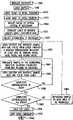
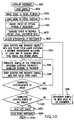
- FIG. 8is a flow diagram illustrating the basic steps implemented in the system of FIG. 1 .
- the various electronics of the system shown in FIG. 1may be initialized 1000 by the computer to initiate the process.
- a thin film samplee.g., a silicon thin film
- the sample translation stagemay be moved into an initial position 1015 , which may include an alignment with respect to reference features on the sample.
- the various optical components of the systemmay be focused 1020 if necessary.
- the lasermay then be stabilized 1025 to a desired energy level and repetition rate, as needed to fully melt the sample in accordance with the particular processing to be carried out. If necessary, the attenuation of the laser pulses may be finely adjusted 1030 .
- the shuttermay be opened 1035 to expose the sample to a single pulse of irradiation through a masking arrangement including at least one of diamond shaped areas, oval shaped areas, and round shaped areas, and accordingly, to commence the sequential lateral solidification process.
- the samplemay be translated in the horizontal direction 1040 .
- the shutteris again opened 1045 exposing previously unmelted regions to a single pulse of irradiation.
- the process of sample translation and irradiation 1040 , 1045may be repeated 1060 to grow the polycrystalline region.
- the sampleis repositioned 1065 , 1066 and the crystallization process is repeated on the new region. If no further regions have been designated for crystallization, the laser is shut off 1070 , the hardware is shut down 1075 , and the process is completed 1080 .
- steps 1005 , 1010 , and 1035 - 1065can be repeated on each sample.
Landscapes
- Physics & Mathematics (AREA)
- Engineering & Computer Science (AREA)
- Optics & Photonics (AREA)
- Power Engineering (AREA)
- Computer Hardware Design (AREA)
- Microelectronics & Electronic Packaging (AREA)
- Manufacturing & Machinery (AREA)
- Condensed Matter Physics & Semiconductors (AREA)
- General Physics & Mathematics (AREA)
- Chemical & Material Sciences (AREA)
- Crystallography & Structural Chemistry (AREA)
- High Energy & Nuclear Physics (AREA)
- Health & Medical Sciences (AREA)
- Toxicology (AREA)
- Electromagnetism (AREA)
- Plasma & Fusion (AREA)
- Mechanical Engineering (AREA)
- Recrystallisation Techniques (AREA)
- Crystals, And After-Treatments Of Crystals (AREA)
Abstract
Description
Claims (24)
Priority Applications (3)
| Application Number | Priority Date | Filing Date | Title |
|---|---|---|---|
| US11/373,773US7638728B2 (en) | 2003-09-16 | 2006-03-10 | Enhancing the width of polycrystalline grains with mask |
| US12/644,273US8063338B2 (en) | 2003-09-16 | 2009-12-22 | Enhancing the width of polycrystalline grains with mask |
| US13/273,687US20120034794A1 (en) | 2003-09-16 | 2011-10-14 | Enhancing the width of polycrystalline grains with mask |
Applications Claiming Priority (3)
| Application Number | Priority Date | Filing Date | Title |
|---|---|---|---|
| US50343703P | 2003-09-16 | 2003-09-16 | |
| PCT/US2004/030326WO2005029547A2 (en) | 2003-09-16 | 2004-09-16 | Enhancing the width of polycrystalline grains with mask |
| US11/373,773US7638728B2 (en) | 2003-09-16 | 2006-03-10 | Enhancing the width of polycrystalline grains with mask |
Related Parent Applications (1)
| Application Number | Title | Priority Date | Filing Date |
|---|---|---|---|
| PCT/US2004/030326ContinuationWO2005029547A2 (en) | 2003-09-16 | 2004-09-16 | Enhancing the width of polycrystalline grains with mask |
Related Child Applications (1)
| Application Number | Title | Priority Date | Filing Date |
|---|---|---|---|
| US12/644,273ContinuationUS8063338B2 (en) | 2003-09-16 | 2009-12-22 | Enhancing the width of polycrystalline grains with mask |
Publications (2)
| Publication Number | Publication Date |
|---|---|
| US20070012664A1 US20070012664A1 (en) | 2007-01-18 |
| US7638728B2true US7638728B2 (en) | 2009-12-29 |
Family
ID=34375351
Family Applications (3)
| Application Number | Title | Priority Date | Filing Date |
|---|---|---|---|
| US11/373,773Active2025-11-24US7638728B2 (en) | 2003-09-16 | 2006-03-10 | Enhancing the width of polycrystalline grains with mask |
| US12/644,273Expired - Fee RelatedUS8063338B2 (en) | 2003-09-16 | 2009-12-22 | Enhancing the width of polycrystalline grains with mask |
| US13/273,687AbandonedUS20120034794A1 (en) | 2003-09-16 | 2011-10-14 | Enhancing the width of polycrystalline grains with mask |
Family Applications After (2)
| Application Number | Title | Priority Date | Filing Date |
|---|---|---|---|
| US12/644,273Expired - Fee RelatedUS8063338B2 (en) | 2003-09-16 | 2009-12-22 | Enhancing the width of polycrystalline grains with mask |
| US13/273,687AbandonedUS20120034794A1 (en) | 2003-09-16 | 2011-10-14 | Enhancing the width of polycrystalline grains with mask |
Country Status (3)
| Country | Link |
|---|---|
| US (3) | US7638728B2 (en) |
| TW (1) | TWI366859B (en) |
| WO (1) | WO2005029547A2 (en) |
Cited By (4)
| Publication number | Priority date | Publication date | Assignee | Title |
|---|---|---|---|---|
| US8063338B2 (en) | 2003-09-16 | 2011-11-22 | The Trustees Of Columbia In The City Of New York | Enhancing the width of polycrystalline grains with mask |
| US8278659B2 (en) | 1996-05-28 | 2012-10-02 | The Trustees Of Columbia University In The City Of New York | Uniform large-grained and grain boundary location manipulated polycrystalline thin film semiconductors formed using sequential lateral solidification and devices formed thereon |
| US8411713B2 (en) | 2002-08-19 | 2013-04-02 | The Trustees Of Columbia University In The City Of New York | Process and system for laser crystallization processing of film regions on a substrate to minimize edge areas, and structure of such film regions |
| TWI704697B (en)* | 2018-10-23 | 2020-09-11 | 宸鴻光電科技股份有限公司 | Semiconductor device and manufacturing method for the same |
Families Citing this family (28)
| Publication number | Priority date | Publication date | Assignee | Title |
|---|---|---|---|---|
| WO2004017380A2 (en)* | 2002-08-19 | 2004-02-26 | The Trustees Of Columbia University In The City Of New York | A single-shot semiconductor processing system and method having various irradiation patterns |
| WO2004075263A2 (en)* | 2003-02-19 | 2004-09-02 | The Trustees Of Columbia University In The City Of New York | System and process for processing a plurality of semiconductor thin films which are crystallized using sequential lateral solidification techniques |
| US7164152B2 (en) | 2003-09-16 | 2007-01-16 | The Trustees Of Columbia University In The City Of New York | Laser-irradiated thin films having variable thickness |
| US7364952B2 (en)* | 2003-09-16 | 2008-04-29 | The Trustees Of Columbia University In The City Of New York | Systems and methods for processing thin films |
| WO2005029546A2 (en) | 2003-09-16 | 2005-03-31 | The Trustees Of Columbia University In The City Of New York | Method and system for providing a continuous motion sequential lateral solidification for reducing or eliminating artifacts, and a mask for facilitating such artifact reduction/elimination |
| US7318866B2 (en)* | 2003-09-16 | 2008-01-15 | The Trustees Of Columbia University In The City Of New York | Systems and methods for inducing crystallization of thin films using multiple optical paths |
| TWI351713B (en) | 2003-09-16 | 2011-11-01 | Univ Columbia | Method and system for providing a single-scan, con |
| TWI359441B (en) | 2003-09-16 | 2012-03-01 | Univ Columbia | Processes and systems for laser crystallization pr |
| WO2005034193A2 (en)* | 2003-09-19 | 2005-04-14 | The Trustees Of Columbia University In The City Ofnew York | Single scan irradiation for crystallization of thin films |
| US7645337B2 (en)* | 2004-11-18 | 2010-01-12 | The Trustees Of Columbia University In The City Of New York | Systems and methods for creating crystallographic-orientation controlled poly-silicon films |
| US8221544B2 (en) | 2005-04-06 | 2012-07-17 | The Trustees Of Columbia University In The City Of New York | Line scan sequential lateral solidification of thin films |
| KR100796590B1 (en)* | 2005-07-12 | 2008-01-21 | 삼성에스디아이 주식회사 | Method for manufacturing polycrystalline silicon thin film, mask pattern used therein and method for manufacturing flat display device using same |
| TWI524384B (en)* | 2005-08-16 | 2016-03-01 | 紐約市哥倫比亞大學理事會 | High-capacity crystallization of the film layer |
| TWI299431B (en)* | 2005-08-23 | 2008-08-01 | Au Optronics Corp | A mask for sequential lateral solidification (sls) process and a method thereof |
| US8598588B2 (en)* | 2005-12-05 | 2013-12-03 | The Trustees Of Columbia University In The City Of New York | Systems and methods for processing a film, and thin films |
| TW200942935A (en) | 2007-09-21 | 2009-10-16 | Univ Columbia | Collections of laterally crystallized semiconductor islands for use in thin film transistors and systems and methods for making same |
| JP5385289B2 (en) | 2007-09-25 | 2014-01-08 | ザ トラスティーズ オブ コロンビア ユニヴァーシティ イン ザ シティ オブ ニューヨーク | Method for producing high uniformity in thin film transistor devices fabricated on laterally crystallized thin films |
| WO2009067688A1 (en) | 2007-11-21 | 2009-05-28 | The Trustees Of Columbia University In The City Of New York | Systems and methods for preparing epitaxially textured polycrystalline films |
| WO2009067687A1 (en)* | 2007-11-21 | 2009-05-28 | The Trustees Of Columbia University In The City Of New York | Systems and methods for preparation of epitaxially textured thick films |
| US8012861B2 (en) | 2007-11-21 | 2011-09-06 | The Trustees Of Columbia University In The City Of New York | Systems and methods for preparing epitaxially textured polycrystalline films |
| US8569155B2 (en)* | 2008-02-29 | 2013-10-29 | The Trustees Of Columbia University In The City Of New York | Flash lamp annealing crystallization for large area thin films |
| US20110175099A1 (en)* | 2008-02-29 | 2011-07-21 | The Trustees Of Columbia University In The City Of New York | Lithographic method of making uniform crystalline si films |
| WO2009111326A2 (en)* | 2008-02-29 | 2009-09-11 | The Trustees Of Columbia University In The City Of New York | Flash light annealing for thin films |
| JP2012508985A (en)* | 2008-11-14 | 2012-04-12 | ザ トラスティーズ オブ コロンビア ユニヴァーシティ イン ザ シティ オブ ニューヨーク | System and method for thin film crystallization |
| US9646831B2 (en) | 2009-11-03 | 2017-05-09 | The Trustees Of Columbia University In The City Of New York | Advanced excimer laser annealing for thin films |
| US9087696B2 (en) | 2009-11-03 | 2015-07-21 | The Trustees Of Columbia University In The City Of New York | Systems and methods for non-periodic pulse partial melt film processing |
| US8440581B2 (en)* | 2009-11-24 | 2013-05-14 | The Trustees Of Columbia University In The City Of New York | Systems and methods for non-periodic pulse sequential lateral solidification |
| KR101135537B1 (en)* | 2010-07-16 | 2012-04-13 | 삼성모바일디스플레이주식회사 | Laser irradiation apparatus |
Citations (202)
| Publication number | Priority date | Publication date | Assignee | Title |
|---|---|---|---|---|
| US3632205A (en) | 1969-01-29 | 1972-01-04 | Thomson Csf | Electro-optical image-tracing systems, particularly for use with laser beams |
| US4234358A (en) | 1979-04-05 | 1980-11-18 | Western Electric Company, Inc. | Patterned epitaxial regrowth using overlapping pulsed irradiation |
| US4309225A (en) | 1979-09-13 | 1982-01-05 | Massachusetts Institute Of Technology | Method of crystallizing amorphous material with a moving energy beam |
| US4382658A (en) | 1980-11-24 | 1983-05-10 | Hughes Aircraft Company | Use of polysilicon for smoothing of liquid crystal MOS displays |
| US4456371A (en) | 1982-06-30 | 1984-06-26 | International Business Machines Corporation | Optical projection printing threshold leveling arrangement |
| US4514895A (en)* | 1983-04-20 | 1985-05-07 | Mitsubishi Denki Kabushiki Kaisha | Method of forming field-effect transistors using selectively beam-crystallized polysilicon channel regions |
| US4639277A (en) | 1984-07-02 | 1987-01-27 | Eastman Kodak Company | Semiconductor material on a substrate, said substrate comprising, in order, a layer of organic polymer, a layer of metal or metal alloy and a layer of dielectric material |
| US4691983A (en) | 1983-10-14 | 1987-09-08 | Hitachi, Ltd. | Optical waveguide and method for making the same |
| JPS62181419U (en) | 1986-05-12 | 1987-11-18 | ||
| US4727047A (en) | 1980-04-10 | 1988-02-23 | Massachusetts Institute Of Technology | Method of producing sheets of crystalline material |
| US4758533A (en) | 1987-09-22 | 1988-07-19 | Xmr Inc. | Laser planarization of nonrefractory metal during integrated circuit fabrication |
| US4793694A (en) | 1986-04-23 | 1988-12-27 | Quantronix Corporation | Method and apparatus for laser beam homogenization |
| US4800179A (en) | 1986-06-13 | 1989-01-24 | Fujitsu Limited | Method for fabricating semiconductor device |
| US4855014A (en) | 1986-01-24 | 1989-08-08 | Sharp Kabushiki Kaisha | Method for manufacturing semiconductor devices |
| US4870031A (en) | 1985-10-07 | 1989-09-26 | Kozo Iizuka, Director General, Agency Of Industrial Science And Technology | Method of manufacturing a semiconductor device |
| US4940505A (en) | 1988-12-02 | 1990-07-10 | Eaton Corporation | Method for growing single crystalline silicon with intermediate bonding agent and combined thermal and photolytic activation |
| US4970546A (en) | 1988-04-07 | 1990-11-13 | Nikon Corporation | Exposure control device |
| US4976809A (en) | 1989-12-18 | 1990-12-11 | North American Philips Corp, Signetics Division | Method of forming an aluminum conductor with highly oriented grain structure |
| US4977104A (en) | 1988-06-01 | 1990-12-11 | Matsushita Electric Industrial Co., Ltd. | Method for producing a semiconductor device by filling hollows with thermally decomposed doped and undoped polysilicon |
| US5032233A (en) | 1990-09-05 | 1991-07-16 | Micron Technology, Inc. | Method for improving step coverage of a metallization layer on an integrated circuit by use of a high melting point metal as an anti-reflective coating during laser planarization |
| US5061655A (en) | 1990-02-16 | 1991-10-29 | Mitsubishi Denki Kabushiki Kaisha | Method of producing SOI structures |
| USRE33836E (en) | 1987-10-22 | 1992-03-03 | Mrs Technology, Inc. | Apparatus and method for making large area electronic devices, such as flat panel displays and the like, using correlated, aligned dual optical systems |
| JPH0433327Y2 (en) | 1985-04-19 | 1992-08-10 | ||
| US5145808A (en) | 1990-08-22 | 1992-09-08 | Sony Corporation | Method of crystallizing a semiconductor thin film |
| US5204659A (en) | 1987-11-13 | 1993-04-20 | Honeywell Inc. | Apparatus and method for providing a gray scale in liquid crystal flat panel displays |
| US5233207A (en) | 1990-06-25 | 1993-08-03 | Nippon Steel Corporation | MOS semiconductor device formed on insulator |
| US5285236A (en) | 1992-09-30 | 1994-02-08 | Kanti Jain | Large-area, high-throughput, high-resolution projection imaging system |
| US5291240A (en) | 1992-10-27 | 1994-03-01 | Anvik Corporation | Nonlinearity-compensated large-area patterning system |
| US5304357A (en) | 1991-05-15 | 1994-04-19 | Ricoh Co. Ltd. | Apparatus for zone melting recrystallization of thin semiconductor film |
| US5373803A (en) | 1991-10-04 | 1994-12-20 | Sony Corporation | Method of epitaxial growth of semiconductor |
| US5395481A (en) | 1993-10-18 | 1995-03-07 | Regents Of The University Of California | Method for forming silicon on a glass substrate |
| US5409867A (en) | 1993-06-16 | 1995-04-25 | Fuji Electric Co., Ltd. | Method of producing polycrystalline semiconductor thin film |
| US5413958A (en) | 1992-11-16 | 1995-05-09 | Tokyo Electron Limited | Method for manufacturing a liquid crystal display substrate |
| US5417897A (en)* | 1993-05-10 | 1995-05-23 | Hewlett-Packard Company | Method for forming tapered inkjet nozzles |
| US5436095A (en)* | 1991-07-11 | 1995-07-25 | Hitachi, Ltd. | Manufacturing method or an exposing method for a semiconductor device for a semiconductor integrated circuit device and a mask used therefor |
| US5453594A (en) | 1993-10-06 | 1995-09-26 | Electro Scientific Industries, Inc. | Radiation beam position and emission coordination system |
| US5456763A (en) | 1994-03-29 | 1995-10-10 | The Regents Of The University Of California | Solar cells utilizing pulsed-energy crystallized microcrystalline/polycrystalline silicon |
| EP0681316A2 (en) | 1994-05-02 | 1995-11-08 | Sony Corporation | Method of processing a thin film on a substrate for display |
| US5466908A (en) | 1992-02-18 | 1995-11-14 | Fujitsu Limited | Method and apparatus for cutting patterns of printed wiring boards and method and apparatus for cleaning printed wiring boards |
| US5496768A (en) | 1993-12-03 | 1996-03-05 | Casio Computer Co., Ltd. | Method of manufacturing polycrystalline silicon thin film |
| US5512494A (en) | 1993-11-29 | 1996-04-30 | Nec Corporation | Method for manufacturing a thin film transistor having a forward staggered structure |
| US5523193A (en) | 1988-05-31 | 1996-06-04 | Texas Instruments Incorporated | Method and apparatus for patterning and imaging member |
| US5529951A (en) | 1993-11-02 | 1996-06-25 | Sony Corporation | Method of forming polycrystalline silicon layer on substrate by large area excimer laser irradiation |
| US5591668A (en) | 1994-03-14 | 1997-01-07 | Matsushita Electric Industrial Co., Ltd. | Laser annealing method for a semiconductor thin film |
| US5614421A (en) | 1994-03-11 | 1997-03-25 | United Microelectronics Corp. | Method of fabricating junction termination extension structure for high-voltage diode devices |
| US5614426A (en) | 1993-08-10 | 1997-03-25 | Semiconductor Energy Laboratory Co., Ltd. | Method of manufacturing semiconductor device having different orientations of crystal channel growth |
| US5616506A (en) | 1993-08-27 | 1997-04-01 | Semiconductor Energy Laboratory Co., Ltd. | Semiconductor device having a crystallized silicon thin film in which the crystallization direction is oriented either vertically or horizontally to the current flow direction |
| US5620910A (en) | 1994-06-23 | 1997-04-15 | Semiconductor Energy Laboratory Co., Ltd. | Method for producing semiconductor device with a gate insulating film consisting of silicon oxynitride |
| WO1997045827A1 (en) | 1996-05-28 | 1997-12-04 | The Trustees Of Columbia University In The City Of New York | Crystallization processing of semiconductor film regions on a substrate, and devices made therewith |
| US5710050A (en) | 1994-08-25 | 1998-01-20 | Sharp Kabushiki Kaisha | Method for fabricating a semiconductor device |
| US5721606A (en) | 1995-09-07 | 1998-02-24 | Jain; Kanti | Large-area, high-throughput, high-resolution, scan-and-repeat, projection patterning system employing sub-full mask |
| US5736709A (en) | 1996-08-12 | 1998-04-07 | Armco Inc. | Descaling metal with a laser having a very short pulse width and high average power |
| US5742426A (en) | 1995-05-25 | 1998-04-21 | York; Kenneth K. | Laser beam treatment pattern smoothing device and laser beam treatment pattern modulator |
| US5756364A (en) | 1994-11-29 | 1998-05-26 | Semiconductor Energy Laboratory Co., Ltd. | Laser processing method of semiconductor device using a catalyst |
| WO1998024118A1 (en) | 1996-11-28 | 1998-06-04 | Philips Electronics N.V. | Electronic device manufacture by energy beam crystallisation |
| US5766989A (en) | 1994-12-27 | 1998-06-16 | Matsushita Electric Industrial Co., Ltd. | Method for forming polycrystalline thin film and method for fabricating thin-film transistor |
| US5844588A (en) | 1995-01-11 | 1998-12-01 | Texas Instruments Incorporated | DMD modulated continuous wave light source for xerographic printer |
| US5861991A (en) | 1996-12-19 | 1999-01-19 | Xerox Corporation | Laser beam conditioner using partially reflective mirrors |
| JPH1164883A (en) | 1997-08-12 | 1999-03-05 | Toshiba Corp | Method and apparatus for manufacturing polycrystalline semiconductor thin film |
| US5893990A (en) | 1995-05-31 | 1999-04-13 | Semiconductor Energy Laboratory Co. Ltd. | Laser processing method |
| WO1999031719A1 (en) | 1997-12-17 | 1999-06-24 | Matsushita Electric Industrial Co., Ltd. | Semiconductor thin film, method of producing the same, apparatus for producing the same, semiconductor device and method of producing the same |
| JPH11281997A (en) | 1998-03-26 | 1999-10-15 | Toshiba Corp | Circuit board, manufacturing method thereof and liquid crystal display device |
| US5986807A (en) | 1997-01-13 | 1999-11-16 | Xerox Corporation | Single binary optical element beam homogenizer |
| US6014944A (en) | 1997-09-19 | 2000-01-18 | The United States Of America As Represented By The Secretary Of The Navy | Apparatus for improving crystalline thin films with a contoured beam pulsed laser |
| DE19839718A1 (en) | 1998-09-01 | 2000-03-02 | Strunk Horst P | Laser crystallization or crystal structure alteration of amorphous or polycrystalline semiconductor layers comprises paired laser pulse irradiation for extended melt time while maintaining a low substrate temperature |
| WO2000014784A1 (en) | 1998-09-04 | 2000-03-16 | Koninklijke Philips Electronics N.V. | Double-pulse laser crystallisation of thin semiconductor films |
| US6072631A (en) | 1998-07-09 | 2000-06-06 | 3M Innovative Properties Company | Diffractive homogenizer with compensation for spatial coherence |
| US6081381A (en) | 1998-10-26 | 2000-06-27 | Polametrics, Inc. | Apparatus and method for reducing spatial coherence and for improving uniformity of a light beam emitted from a coherent light source |
| US6093934A (en) | 1996-01-19 | 2000-07-25 | Semiconductor Energy Laboratory Co., Ltd. | Thin film transistor having grain boundaries with segregated oxygen and halogen elements |
| US6117301A (en) | 1997-09-24 | 2000-09-12 | Degussa-Huls Aktiengesellschaft | Electrolyte for the galvanic deposition of low-stress, crack-resistant ruthenium layers |
| GB2338343B (en) | 1998-06-09 | 2000-09-13 | Lg Lcd Inc | Method for fabricating thin film transistor |
| US6120976A (en) | 1998-11-20 | 2000-09-19 | 3M Innovative Properties Company | Laser ablated feature formation method |
| US6130455A (en) | 1996-03-21 | 2000-10-10 | Sharp Kabushiki Kaisha | Semiconductor device, thin film transistor having an active crystal layer formed by a line containing a catalyst element |
| US6130009A (en) | 1994-01-03 | 2000-10-10 | Litel Instruments | Apparatus and process for nozzle production utilizing computer generated holograms |
| GB2338342B (en) | 1998-06-09 | 2000-10-11 | Lg Lcd Inc | Method for crystalizing amorphous silicon layer and method for fabricating tft |
| US6162711A (en) | 1999-01-15 | 2000-12-19 | Lucent Technologies, Inc. | In-situ boron doped polysilicon with dual layer and dual grain structure for use in integrated circuits manufacturing |
| GB2338597B (en) | 1998-06-09 | 2001-01-03 | Lg Lcd Inc | Method of fabricating thin film transistors for a liquid crystal display |
| US6172820B1 (en) | 1998-06-08 | 2001-01-09 | Sanyo Electric Co., Ltd. | Laser irradiation device |
| JP2001023920A (en) | 1999-07-08 | 2001-01-26 | Sumitomo Heavy Ind Ltd | Laser processor |
| US6187088B1 (en) | 1998-08-03 | 2001-02-13 | Nec Corporation | Laser irradiation process |
| US6190985B1 (en) | 1999-08-17 | 2001-02-20 | Advanced Micro Devices, Inc. | Practical way to remove heat from SOI devices |
| US6193796B1 (en) | 1998-01-24 | 2001-02-27 | Lg. Philips Lcd Co, Ltd. | Method of crystallizing silicon layer |
| US6198141B1 (en)* | 1996-08-13 | 2001-03-06 | Semiconductor Energy Laboratory Co., Ltd. | Insulated gate semiconductor device and method of manufacturing the same |
| WO2001018854A1 (en) | 1999-09-03 | 2001-03-15 | The Trustees Of Columbia University In The City Of New York | Methods for producing uniform large-grained and grain boundary location manipulated polycrystalline thin film semiconductors using sequential lateral solidification |
| US6203952B1 (en) | 1999-01-14 | 2001-03-20 | 3M Innovative Properties Company | Imaged article on polymeric substrate |
| WO2001018855A8 (en) | 1999-09-03 | 2001-04-19 | Univ Columbia | Systems and methods using sequential lateral solidification for producing single or polycrystalline silicon thin films at low temperatures |
| US6222195B1 (en) | 1996-01-24 | 2001-04-24 | Fujitsu Limited | Charged-particle-beam exposure device and charged-particle-beam exposure method |
| US6235614B1 (en) | 1998-06-09 | 2001-05-22 | Lg. Philips Lcd Co., Ltd. | Methods of crystallizing amorphous silicon layer and fabricating thin film transistor using the same |
| US6242291B1 (en) | 1996-12-12 | 2001-06-05 | Semiconductor Energy Laboratory Co., Ltd. | Laser annealing method and laser annealing device |
| US6255146B1 (en) | 1993-06-10 | 2001-07-03 | Mitsubishi Denki Kabushiki Kaisha | Thin film transistor and a method of manufacturing thereof |
| US6274488B1 (en) | 2000-04-12 | 2001-08-14 | Ultratech Stepper, Inc. | Method of forming a silicide region in a Si substrate and a device having same |
| US6285001B1 (en) | 1995-04-26 | 2001-09-04 | 3M Innovative Properties Company | Method and apparatus for step and repeat exposures |
| WO2001071791A1 (en) | 2000-03-21 | 2001-09-27 | The Trustees Of Columbia University In The City Of New York | Surface planarization of thin silicon films during and after processing by the sequential lateral solidification method |
| WO2001071786A1 (en) | 2000-03-16 | 2001-09-27 | The Trustees Of Columbia University In The City Of New York | Method and system for providing a continuous motion sequential lateral solidification |
| US6313435B1 (en) | 1998-11-20 | 2001-11-06 | 3M Innovative Properties Company | Mask orbiting for laser ablated feature formation |
| US6316338B1 (en) | 1999-06-28 | 2001-11-13 | Lg. Philips Lcd Co., Ltd. | Laser annealing method |
| US6320227B1 (en) | 1998-12-26 | 2001-11-20 | Hyundai Electronics Industries Co., Ltd. | Semiconductor memory device and method for fabricating the same |
| US6333232B1 (en) | 1999-11-11 | 2001-12-25 | Mitsubishi Denki Kabushiki Kaisha | Semiconductor device and method of manufacturing the same |
| US6341042B1 (en) | 1999-01-29 | 2002-01-22 | Kabushiki Kaisha Toshiba | Laser radiating apparatus and methods for manufacturing a polycrystalline semiconductor film and a liquid crystal display device |
| US6348990B1 (en) | 1998-06-18 | 2002-02-19 | Hamamatsu Photonics K.K. | Spatial light modulator and spatial light modulating method |
| US6353218B1 (en) | 1997-12-17 | 2002-03-05 | Semiconductor Energy Laboratory Co., Ltd. | Laser illumination apparatus with beam dividing and combining performances |
| US6358784B1 (en) | 1992-03-26 | 2002-03-19 | Semiconductor Energy Laboratory Co., Ltd. | Process for laser processing and apparatus for use in the same |
| US6388146B1 (en) | 1998-01-28 | 2002-05-14 | Sharp Kabushiki Kaisha | Polymerizable compound, polymerizable resin composition, cured polymer and liquid crystal display device |
| US6388386B1 (en) | 1999-04-19 | 2002-05-14 | Sony Corporation | Process of crystallizing semiconductor thin film and laser irradiation |
| US6393042B1 (en) | 1999-03-08 | 2002-05-21 | Semiconductor Energy Laboratory Co., Ltd. | Beam homogenizer and laser irradiation apparatus |
| US6392810B1 (en) | 1998-10-05 | 2002-05-21 | Semiconductor Energy Laboratory Co., Ltd. | Laser irradiation apparatus, laser irradiation method, beam homogenizer, semiconductor device, and method of manufacturing the semiconductor device |
| WO2002042847A1 (en) | 2000-11-27 | 2002-05-30 | The Trustees Of Columbia University In The City Of New York | Process and mask projection system for laser crystallization processing of semiconductor film regions on a substrate |
| US6407012B1 (en) | 1997-12-26 | 2002-06-18 | Seiko Epson Corporation | Method of producing silicon oxide film, method of manufacturing semiconductor device, semiconductor device, display and infrared irradiating device |
| US6410373B1 (en) | 2001-04-24 | 2002-06-25 | United Microelectronics Corp. | Method of forming polysilicon thin film transistor structure |
| US20020083557A1 (en) | 2000-12-28 | 2002-07-04 | Yun-Ho Jung | Apparatus and method of crystallizing amorphous silicon |
| US20020096680A1 (en) | 1999-01-08 | 2002-07-25 | Yukiyasu Sugano | Process for producing thin film semiconductor device and laser irradiation apparatus |
| DE10103670A1 (en) | 2001-01-27 | 2002-08-01 | Christiansen Jens I | Generation of crystalline Si layers with (100) texture by laser bombardment of amorphous Si layers on a substrate |
| US6429100B2 (en) | 1996-05-31 | 2002-08-06 | Sanyo Electric Co., Ltd. | Method of manufacturing a semiconductor device |
| US20020104750A1 (en) | 2001-02-08 | 2002-08-08 | Hiroshi Ito | Laser processing method and apparatus |
| US6432758B1 (en) | 2000-08-09 | 2002-08-13 | Huang-Chung Cheng | Recrystallization method of polysilicon film in thin film transistor |
| US20020119609A1 (en) | 2001-01-29 | 2002-08-29 | Mutsuko Hatano | Thin film semiconductor device, polycrystalline semiconductor thin film production process and production apparatus |
| US6445359B1 (en) | 2000-09-29 | 2002-09-03 | Hughes Electronics Corporation | Low noise block down converter adapter with built-in multi-switch for a satellite dish antenna |
| US6444506B1 (en) | 1995-10-25 | 2002-09-03 | Semiconductor Energy Laboratory Co., Ltd. | Method of manufacturing silicon thin film devices using laser annealing in a hydrogen mixture gas followed by nitride formation |
| US6448612B1 (en) | 1992-12-09 | 2002-09-10 | Semiconductor Energy Laboratory Co., Ltd. | Pixel thin film transistor and a driver circuit for driving the pixel thin film transistor |
| US6451631B1 (en) | 2000-08-10 | 2002-09-17 | Hitachi America, Ltd. | Thin film crystal growth by laser annealing |
| WO2002031869A3 (en) | 2000-10-10 | 2002-09-19 | Univ Columbia | Method and apparatus for processing thin metal layers |
| US6455359B1 (en) | 1997-02-13 | 2002-09-24 | Semiconductor Energy Laboratory Co., Ltd. | Laser-irradiation method and laser-irradiation device |
| US20020151115A1 (en) | 2000-09-05 | 2002-10-17 | Sony Corporation | Process for production of thin film, semiconductor thin film, semiconductor device, process for production of semiconductor thin film, and apparatus for production of semiconductor thin film |
| US6468845B1 (en) | 1992-12-25 | 2002-10-22 | Hitachi, Ltd. | Semiconductor apparatus having conductive thin films and manufacturing apparatus therefor |
| US6471772B1 (en) | 1997-04-17 | 2002-10-29 | Semiconductor Energy Laboratory Co., Ltd. | Laser processing apparatus and laser processing method |
| US6472684B1 (en) | 1997-09-20 | 2002-10-29 | Semiconductor Energy Laboratories Co., Ltd. | Nonvolatile memory and manufacturing method thereof |
| WO2002086955A1 (en) | 2001-04-23 | 2002-10-31 | Koninklijke Philips Electronics N.V. | Semiconductor device and method of manufacturing same |
| WO2002086954A1 (en) | 2001-04-19 | 2002-10-31 | The Trustee Of Columbia University In The City Of New York | Method and system for providing a single-scan, continuous motion sequential lateral solidification |
| US6476447B1 (en) | 1992-02-05 | 2002-11-05 | Semiconductor Energy Laboratory Co., Ltd. | Active matrix display device including a transistor |
| US6493042B1 (en) | 1999-03-18 | 2002-12-10 | Xerox Corporation | Feature based hierarchical video segmentation |
| US6495067B1 (en) | 1999-03-01 | 2002-12-17 | Fuji Photo Film Co., Ltd. | Liquid crystal compound, liquid crystal mixture or composition, electrolyte comprising the same, electrochemical cell and photo-electrochemical cell containing the electrolyte |
| US6495405B2 (en) | 2001-01-29 | 2002-12-17 | Sharp Laboratories Of America, Inc. | Method of optimizing channel characteristics using laterally-crystallized ELA poly-Si films |
| US6501095B2 (en) | 2001-01-26 | 2002-12-31 | Hitachi, Ltd. | Thin film transistor |
| US20030003242A1 (en) | 2001-06-28 | 2003-01-02 | Apostolos Voutsas | Pulse width method for controlling lateral growth in crystallized silicon films |
| US20030000455A1 (en) | 2001-06-28 | 2003-01-02 | Apostolos Voutsas | System and method for regulating lateral growth in laser irradiated silicon films |
| US20030006221A1 (en) | 2001-07-06 | 2003-01-09 | Minghui Hong | Method and apparatus for cutting a multi-layer substrate by dual laser irradiation |
| US6506636B2 (en) | 2000-05-12 | 2003-01-14 | Semiconductor Energy Laboratory Co., Ltd. | Method of manufacturing a semiconductor device having a crystallized amorphous silicon film |
| US20030013278A1 (en) | 2001-07-10 | 2003-01-16 | Jin Jang | Method for crystallizing amorphous film and method for fabricating LCD by using the same |
| US20030014337A1 (en) | 2001-07-10 | 2003-01-16 | Mathews Scott H. | Systems, methods and computer program products for performing a generalized contingent claim valuation |
| US6511718B1 (en) | 1997-07-14 | 2003-01-28 | Symetrix Corporation | Method and apparatus for fabrication of thin films by chemical vapor deposition |
| US6512634B2 (en) | 1997-09-30 | 2003-01-28 | Semiconductor Energy Laboratory Co., Ltd. | Beam homogenizer, laser illumination apparatus and method, and semiconductor device |
| US6516009B1 (en) | 1997-02-28 | 2003-02-04 | Semiconductor Energy Laboratory Co., Ltd. | Laser irradiating device and laser irradiating method |
| US6521492B2 (en) | 2000-06-12 | 2003-02-18 | Seiko Epson Corporation | Thin-film semiconductor device fabrication method |
| US6521473B1 (en) | 1999-10-29 | 2003-02-18 | Lgphilips Lcd Co., Ltd. | Method of fabricating a liquid crystal display |
| US6526585B1 (en) | 2001-12-21 | 2003-03-04 | Elton E. Hill | Wet smoke mask |
| WO2003018882A1 (en) | 2001-08-27 | 2003-03-06 | The Trustees Of Columbia University In The City Of New York | Improved polycrystalline tft uniformity through microstructure mis-alignment |
| US6535535B1 (en) | 1999-02-12 | 2003-03-18 | Semiconductor Energy Laboratory Co., Ltd. | Laser irradiation method, laser irradiation apparatus, and semiconductor device |
| US20030068836A1 (en) | 2001-10-10 | 2003-04-10 | Mikio Hongo | Laser annealing apparatus, TFT device and annealing method of the same |
| US6562701B2 (en)* | 2001-03-23 | 2003-05-13 | Matsushita Electric Industrial Co., Ltd. | Method of manufacturing nitride semiconductor substrate |
| US20030089907A1 (en) | 2001-10-12 | 2003-05-15 | Hitachi, Ltd. | Thin-film transistor device, its manufacturing process, and image display using the device |
| US6573163B2 (en) | 2001-01-29 | 2003-06-03 | Sharp Laboratories Of America, Inc. | Method of optimizing channel characteristics using multiple masks to form laterally crystallized ELA poly-Si films |
| WO2003046965A1 (en) | 2001-11-28 | 2003-06-05 | The Trustees Of Columbia University In The City Of New York | Specialized substrates for use in sequential lateral solidification processing |
| US6577380B1 (en) | 2000-07-21 | 2003-06-10 | Anvik Corporation | High-throughput materials processing system |
| US6580053B1 (en) | 2000-08-31 | 2003-06-17 | Sharp Laboratories Of America, Inc. | Apparatus to control the amount of oxygen incorporated into polycrystalline silicon film during excimer laser processing of silicon films |
| US6582827B1 (en) | 2000-11-27 | 2003-06-24 | The Trustees Of Columbia University In The City Of New York | Specialized substrates for use in sequential lateral solidification processing |
| US20030148565A1 (en) | 2001-02-01 | 2003-08-07 | Hideo Yamanaka | Method for forming thin semiconductor film, method for fabricating semiconductor device, system for executing these methods and electrooptic device |
| US6608326B1 (en) | 1999-07-13 | 2003-08-19 | Hitachi, Ltd. | Semiconductor film, liquid-crystal display using semiconductor film, and method of manufacture thereof |
| US6621044B2 (en) | 2001-01-18 | 2003-09-16 | Anvik Corporation | Dual-beam materials-processing system |
| US20030194613A1 (en) | 2002-03-27 | 2003-10-16 | Voutsas Apostolos T. | Method of suppressing energy spikes of a partially-coherent beam |
| US20030196587A1 (en) | 1999-09-23 | 2003-10-23 | Memc Electronic Materials, Inc. | Process for suppressing the nucleation and/or growth of interstitial type defects by controlling the cooling rate through nucleation |
| US6660575B1 (en) | 1991-10-04 | 2003-12-09 | Semiconductor Energy Laboratory Co., Ltd. | Method for forming a semiconductor device |
| US6667198B2 (en) | 2001-07-27 | 2003-12-23 | Kabushiki Kaisha Toshiba | Method and photo mask for manufacturing an array substrate |
| WO2004017382A3 (en) | 2002-08-19 | 2004-04-29 | Univ Columbia | Process and system for laser crystallization processing of film regions on a substrate to provide substantial uniformity within areas in such regions and edge areas thereof, and a structure of such film regions |
| WO2004017381A3 (en) | 2002-08-19 | 2004-05-13 | Univ Columbia | Process and system for laser crystallization processing of film regions on a substrate to minimize edge areas, and structure of such film regions |
| US20040127066A1 (en) | 2002-12-31 | 2004-07-01 | Yun-Ho Jung | Mask for sequential lateral solidification and crystallization method using thereof |
| WO2003084688A3 (en) | 2002-04-01 | 2004-07-15 | Univ Columbia | Method and system for providing a thin film |
| US20040140470A1 (en) | 1999-08-18 | 2004-07-22 | Semiconductor Energy Laboratory Co., Ltd. | Semiconductor device and method of fabricating the same |
| US6767804B2 (en)* | 2001-11-08 | 2004-07-27 | Sharp Laboratories Of America, Inc. | 2N mask design and method of sequential lateral solidification |
| US6770545B2 (en)* | 2001-06-07 | 2004-08-03 | Lg Philips Lcd Co., Ltd. | Amorphous silicon crystallization method |
| US6777276B2 (en) | 2002-08-29 | 2004-08-17 | Sharp Laboratories Of America, Inc. | System and method for optimized laser annealing smoothing mask |
| US6784455B2 (en) | 1998-07-16 | 2004-08-31 | Sharp Laboratories Of America, Inc. | Single crystal TFT from continuous transition metal delivery method |
| US20040169176A1 (en) | 2003-02-28 | 2004-09-02 | Peterson Paul E. | Methods of forming thin film transistors and related systems |
| US20040182838A1 (en) | 2001-04-18 | 2004-09-23 | Das Palash P. | Very high energy, high stability gas discharge laser surface treatment system |
| US20040222187A1 (en) | 2003-05-02 | 2004-11-11 | Kun-Chih Lin | Method of fabricating polysilicon film by excimer laser crystallization process |
| US6830993B1 (en) | 2000-03-21 | 2004-12-14 | The Trustees Of Columbia University In The City Of New York | Surface planarization of thin silicon films during and after processing by the sequential lateral solidification method |
| WO2004075263A3 (en) | 2003-02-19 | 2005-01-20 | Univ Columbia | System and process for processing a plurality of semiconductor thin films which are crystallized using sequential lateral solidification techniques |
| US6858477B2 (en) | 2000-12-21 | 2005-02-22 | Koninklijke Philips Electronics N.V. | Thin film transistors |
| US20050059265A1 (en) | 2003-09-16 | 2005-03-17 | The Trustees Of Columbia University In The City Of New York | Systems and methods for processing thin films |
| WO2005029546A2 (en) | 2003-09-16 | 2005-03-31 | The Trustees Of Columbia University In The City Of New York | Method and system for providing a continuous motion sequential lateral solidification for reducing or eliminating artifacts, and a mask for facilitating such artifact reduction/elimination |
| US20050142451A1 (en) | 2003-12-26 | 2005-06-30 | Lg Philips Lcd Co., Ltd. | Mask for laser crystallization and crystallization method using the same |
| US20050142450A1 (en) | 2003-12-26 | 2005-06-30 | Lg.Philips Lcd Co., Ltd. | Laser beam pattern mask and crystallization method using the same |
| US20050141580A1 (en) | 2001-04-18 | 2005-06-30 | Partlo William N. | Laser thin film poly-silicon annealing system |
| WO2005029550A3 (en) | 2003-09-16 | 2005-09-09 | Univ Columbia | Method and system for producing crystalline thin films with a uniform crystalline orientation |
| US20050202654A1 (en) | 2002-08-19 | 2005-09-15 | Im James S. | Process and system for laser crystallization processing of film regions on a substrate to provide substantial uniformity, and a structure of such film regions |
| WO2004017380A3 (en) | 2002-08-19 | 2005-12-15 | Univ Columbia | A single-shot semiconductor processing system and method having various irradiation patterns |
| WO2005029551A3 (en) | 2003-09-16 | 2005-12-22 | Univ Columbia | Processes and systems for laser crystallization processing of film regions on a substrate utilizing a line-type beam, and structures of such film regions |
| US20060102901A1 (en) | 2004-11-18 | 2006-05-18 | The Trustees Of Columbia University In The City Of New York | Systems and methods for creating crystallographic-orientation controlled poly-Silicon films |
| US7049184B2 (en)* | 2003-05-09 | 2006-05-23 | Nec Corporation | Semiconductor thin film, thin film transistor, method for manufacturing same, and manufacturing equipment of semiconductor thin film |
| US20060125741A1 (en) | 2004-12-08 | 2006-06-15 | Masahiro Tanaka | Display device and driving method thereof |
| US7091411B2 (en) | 2000-08-31 | 2006-08-15 | Institut Fur Physikalische Hochtechnologie E.V. | Multicrystalline laser-crystallized silicon thin layer solar cell deposited on a glass substrate and method of producing |
| US20060211183A1 (en) | 2002-09-30 | 2006-09-21 | Nanosys, Inc. | Large-area nanoenabled macroelectronic substrates and uses therefor |
| US20060254500A1 (en) | 2005-04-06 | 2006-11-16 | The Trustees Of Columbia University In The City Of New York | Line scan sequential lateral solidification of thin films |
| US20070032096A1 (en) | 2003-09-16 | 2007-02-08 | Im James S | System and process for providing multiple beam sequential lateral solidification |
| US7187016B2 (en) | 2001-01-26 | 2007-03-06 | Exploitation Of Next Generation Co., Ltd | Semiconductor device |
| US7217605B2 (en) | 2000-11-29 | 2007-05-15 | Semiconductor Energy Laboratory Co., Ltd. | Laser irradiation method and method of manufacturing a semiconductor device |
| US20070108472A1 (en) | 2005-11-16 | 2007-05-17 | Jeong Jae K | Thin film transistor and method of manufacturing the same |
| US20070111349A1 (en) | 2003-09-16 | 2007-05-17 | James Im | Laser-irradiated thin films having variable thickness |
| US20070215942A1 (en) | 2006-03-17 | 2007-09-20 | Industrial Technology Research Institute | Thin film transistor device with high symmetry |
| US7297982B2 (en) | 1999-01-11 | 2007-11-20 | Hitachi, Ltd. | Semiconductor device including a TFT having large-grain polycrystalline active layer, LCD employing the same and method of fabricating them |
| US7311778B2 (en) | 2003-09-19 | 2007-12-25 | The Trustees Of Columbia University In The City Of New York | Single scan irradiation for crystallization of thin films |
| EP1067593B1 (en) | 1999-07-08 | 2008-12-24 | Nec Corporation | Semiconductor thin film forming system |
| JP4279064B2 (en) | 2003-06-27 | 2009-06-17 | 三菱化学株式会社 | Porous silica film and laminate having the same |
Family Cites Families (11)
| Publication number | Priority date | Publication date | Assignee | Title |
|---|---|---|---|---|
| JPH08236443A (en)* | 1995-02-28 | 1996-09-13 | Fuji Xerox Co Ltd | Semiconductor crystal growing method and semiconductor manufacturing device |
| JP3645378B2 (en) | 1996-01-19 | 2005-05-11 | 株式会社半導体エネルギー研究所 | Method for manufacturing semiconductor device |
| US6599790B1 (en) | 1996-02-15 | 2003-07-29 | Semiconductor Energy Laboratory Co., Ltd | Laser-irradiation method and laser-irradiation device |
| US5981974A (en) | 1996-09-30 | 1999-11-09 | Sharp Kabushiki Kaisha | Semiconductor device and method for fabricating the same |
| US6699671B1 (en)* | 1998-09-24 | 2004-03-02 | Pharmacia & Upjohn Company | Alzheimer's disease secretase, APP substrates therefor, and uses therefor |
| US6746942B2 (en) | 2000-09-05 | 2004-06-08 | Sony Corporation | Semiconductor thin film and method of fabricating semiconductor thin film, apparatus for fabricating single crystal semiconductor thin film, and method of fabricating single crystal thin film, single crystal thin film substrate, and semiconductor device |
| US7192479B2 (en)* | 2002-04-17 | 2007-03-20 | Sharp Laboratories Of America, Inc. | Laser annealing mask and method for smoothing an annealed surface |
| US6635836B1 (en)* | 2002-04-18 | 2003-10-21 | Oil-Rite Corporation | Housing contained fluid flow switch and indicator |
| KR100997275B1 (en)* | 2003-06-12 | 2010-11-29 | 엘지디스플레이 주식회사 | Silicon Crystallization Method |
| WO2005029547A2 (en) | 2003-09-16 | 2005-03-31 | The Trustees Of Columbia University In The City Of New York | Enhancing the width of polycrystalline grains with mask |
| TWI351713B (en) | 2003-09-16 | 2011-11-01 | Univ Columbia | Method and system for providing a single-scan, con |
- 2004
- 2004-09-16WOPCT/US2004/030326patent/WO2005029547A2/enactiveApplication Filing
- 2004-09-16TWTW093128077Apatent/TWI366859B/ennot_activeIP Right Cessation
- 2006
- 2006-03-10USUS11/373,773patent/US7638728B2/enactiveActive
- 2009
- 2009-12-22USUS12/644,273patent/US8063338B2/ennot_activeExpired - Fee Related
- 2011
- 2011-10-14USUS13/273,687patent/US20120034794A1/ennot_activeAbandoned
Patent Citations (242)
| Publication number | Priority date | Publication date | Assignee | Title |
|---|---|---|---|---|
| US3632205A (en) | 1969-01-29 | 1972-01-04 | Thomson Csf | Electro-optical image-tracing systems, particularly for use with laser beams |
| US4234358A (en) | 1979-04-05 | 1980-11-18 | Western Electric Company, Inc. | Patterned epitaxial regrowth using overlapping pulsed irradiation |
| US4309225A (en) | 1979-09-13 | 1982-01-05 | Massachusetts Institute Of Technology | Method of crystallizing amorphous material with a moving energy beam |
| US4727047A (en) | 1980-04-10 | 1988-02-23 | Massachusetts Institute Of Technology | Method of producing sheets of crystalline material |
| US4382658A (en) | 1980-11-24 | 1983-05-10 | Hughes Aircraft Company | Use of polysilicon for smoothing of liquid crystal MOS displays |
| US4456371A (en) | 1982-06-30 | 1984-06-26 | International Business Machines Corporation | Optical projection printing threshold leveling arrangement |
| US4514895A (en)* | 1983-04-20 | 1985-05-07 | Mitsubishi Denki Kabushiki Kaisha | Method of forming field-effect transistors using selectively beam-crystallized polysilicon channel regions |
| US4691983A (en) | 1983-10-14 | 1987-09-08 | Hitachi, Ltd. | Optical waveguide and method for making the same |
| US4639277A (en) | 1984-07-02 | 1987-01-27 | Eastman Kodak Company | Semiconductor material on a substrate, said substrate comprising, in order, a layer of organic polymer, a layer of metal or metal alloy and a layer of dielectric material |
| JPH0433327Y2 (en) | 1985-04-19 | 1992-08-10 | ||
| US4870031A (en) | 1985-10-07 | 1989-09-26 | Kozo Iizuka, Director General, Agency Of Industrial Science And Technology | Method of manufacturing a semiconductor device |
| US4855014A (en) | 1986-01-24 | 1989-08-08 | Sharp Kabushiki Kaisha | Method for manufacturing semiconductor devices |
| US4793694A (en) | 1986-04-23 | 1988-12-27 | Quantronix Corporation | Method and apparatus for laser beam homogenization |
| JPS62181419U (en) | 1986-05-12 | 1987-11-18 | ||
| US4800179A (en) | 1986-06-13 | 1989-01-24 | Fujitsu Limited | Method for fabricating semiconductor device |
| US4758533A (en) | 1987-09-22 | 1988-07-19 | Xmr Inc. | Laser planarization of nonrefractory metal during integrated circuit fabrication |
| USRE33836E (en) | 1987-10-22 | 1992-03-03 | Mrs Technology, Inc. | Apparatus and method for making large area electronic devices, such as flat panel displays and the like, using correlated, aligned dual optical systems |
| US5204659A (en) | 1987-11-13 | 1993-04-20 | Honeywell Inc. | Apparatus and method for providing a gray scale in liquid crystal flat panel displays |
| US4970546A (en) | 1988-04-07 | 1990-11-13 | Nikon Corporation | Exposure control device |
| US5523193A (en) | 1988-05-31 | 1996-06-04 | Texas Instruments Incorporated | Method and apparatus for patterning and imaging member |
| US4977104A (en) | 1988-06-01 | 1990-12-11 | Matsushita Electric Industrial Co., Ltd. | Method for producing a semiconductor device by filling hollows with thermally decomposed doped and undoped polysilicon |
| US4940505A (en) | 1988-12-02 | 1990-07-10 | Eaton Corporation | Method for growing single crystalline silicon with intermediate bonding agent and combined thermal and photolytic activation |
| US4976809A (en) | 1989-12-18 | 1990-12-11 | North American Philips Corp, Signetics Division | Method of forming an aluminum conductor with highly oriented grain structure |
| US5061655A (en) | 1990-02-16 | 1991-10-29 | Mitsubishi Denki Kabushiki Kaisha | Method of producing SOI structures |
| US5233207A (en) | 1990-06-25 | 1993-08-03 | Nippon Steel Corporation | MOS semiconductor device formed on insulator |
| US5145808A (en) | 1990-08-22 | 1992-09-08 | Sony Corporation | Method of crystallizing a semiconductor thin film |
| US5032233A (en) | 1990-09-05 | 1991-07-16 | Micron Technology, Inc. | Method for improving step coverage of a metallization layer on an integrated circuit by use of a high melting point metal as an anti-reflective coating during laser planarization |
| US5304357A (en) | 1991-05-15 | 1994-04-19 | Ricoh Co. Ltd. | Apparatus for zone melting recrystallization of thin semiconductor film |
| US5436095A (en)* | 1991-07-11 | 1995-07-25 | Hitachi, Ltd. | Manufacturing method or an exposing method for a semiconductor device for a semiconductor integrated circuit device and a mask used therefor |
| US5373803A (en) | 1991-10-04 | 1994-12-20 | Sony Corporation | Method of epitaxial growth of semiconductor |
| US6660575B1 (en) | 1991-10-04 | 2003-12-09 | Semiconductor Energy Laboratory Co., Ltd. | Method for forming a semiconductor device |
| US6476447B1 (en) | 1992-02-05 | 2002-11-05 | Semiconductor Energy Laboratory Co., Ltd. | Active matrix display device including a transistor |
| US5466908A (en) | 1992-02-18 | 1995-11-14 | Fujitsu Limited | Method and apparatus for cutting patterns of printed wiring boards and method and apparatus for cleaning printed wiring boards |
| US6358784B1 (en) | 1992-03-26 | 2002-03-19 | Semiconductor Energy Laboratory Co., Ltd. | Process for laser processing and apparatus for use in the same |
| US5285236A (en) | 1992-09-30 | 1994-02-08 | Kanti Jain | Large-area, high-throughput, high-resolution projection imaging system |
| US5291240A (en) | 1992-10-27 | 1994-03-01 | Anvik Corporation | Nonlinearity-compensated large-area patterning system |
| US5413958A (en) | 1992-11-16 | 1995-05-09 | Tokyo Electron Limited | Method for manufacturing a liquid crystal display substrate |
| US6448612B1 (en) | 1992-12-09 | 2002-09-10 | Semiconductor Energy Laboratory Co., Ltd. | Pixel thin film transistor and a driver circuit for driving the pixel thin film transistor |
| US6468845B1 (en) | 1992-12-25 | 2002-10-22 | Hitachi, Ltd. | Semiconductor apparatus having conductive thin films and manufacturing apparatus therefor |
| US5417897A (en)* | 1993-05-10 | 1995-05-23 | Hewlett-Packard Company | Method for forming tapered inkjet nozzles |
| US6255146B1 (en) | 1993-06-10 | 2001-07-03 | Mitsubishi Denki Kabushiki Kaisha | Thin film transistor and a method of manufacturing thereof |
| US5409867A (en) | 1993-06-16 | 1995-04-25 | Fuji Electric Co., Ltd. | Method of producing polycrystalline semiconductor thin film |
| US5614426A (en) | 1993-08-10 | 1997-03-25 | Semiconductor Energy Laboratory Co., Ltd. | Method of manufacturing semiconductor device having different orientations of crystal channel growth |
| US5616506A (en) | 1993-08-27 | 1997-04-01 | Semiconductor Energy Laboratory Co., Ltd. | Semiconductor device having a crystallized silicon thin film in which the crystallization direction is oriented either vertically or horizontally to the current flow direction |
| US5453594A (en) | 1993-10-06 | 1995-09-26 | Electro Scientific Industries, Inc. | Radiation beam position and emission coordination system |
| US5395481A (en) | 1993-10-18 | 1995-03-07 | Regents Of The University Of California | Method for forming silicon on a glass substrate |
| US5529951A (en) | 1993-11-02 | 1996-06-25 | Sony Corporation | Method of forming polycrystalline silicon layer on substrate by large area excimer laser irradiation |
| EP0655774A3 (en) | 1993-11-02 | 1996-07-17 | Sony Corp | Method for manufacturing a polycrystalline silicon layer and surface treatment apparatus used. |
| US5512494A (en) | 1993-11-29 | 1996-04-30 | Nec Corporation | Method for manufacturing a thin film transistor having a forward staggered structure |
| US5496768A (en) | 1993-12-03 | 1996-03-05 | Casio Computer Co., Ltd. | Method of manufacturing polycrystalline silicon thin film |
| US6130009A (en) | 1994-01-03 | 2000-10-10 | Litel Instruments | Apparatus and process for nozzle production utilizing computer generated holograms |
| US5614421A (en) | 1994-03-11 | 1997-03-25 | United Microelectronics Corp. | Method of fabricating junction termination extension structure for high-voltage diode devices |
| US5591668A (en) | 1994-03-14 | 1997-01-07 | Matsushita Electric Industrial Co., Ltd. | Laser annealing method for a semiconductor thin film |
| US5456763A (en) | 1994-03-29 | 1995-10-10 | The Regents Of The University Of California | Solar cells utilizing pulsed-energy crystallized microcrystalline/polycrystalline silicon |
| EP0681316A2 (en) | 1994-05-02 | 1995-11-08 | Sony Corporation | Method of processing a thin film on a substrate for display |
| US5620910A (en) | 1994-06-23 | 1997-04-15 | Semiconductor Energy Laboratory Co., Ltd. | Method for producing semiconductor device with a gate insulating film consisting of silicon oxynitride |
| US5710050A (en) | 1994-08-25 | 1998-01-20 | Sharp Kabushiki Kaisha | Method for fabricating a semiconductor device |
| US5756364A (en) | 1994-11-29 | 1998-05-26 | Semiconductor Energy Laboratory Co., Ltd. | Laser processing method of semiconductor device using a catalyst |
| US5766989A (en) | 1994-12-27 | 1998-06-16 | Matsushita Electric Industrial Co., Ltd. | Method for forming polycrystalline thin film and method for fabricating thin-film transistor |
| US5844588A (en) | 1995-01-11 | 1998-12-01 | Texas Instruments Incorporated | DMD modulated continuous wave light source for xerographic printer |
| US6285001B1 (en) | 1995-04-26 | 2001-09-04 | 3M Innovative Properties Company | Method and apparatus for step and repeat exposures |
| US5742426A (en) | 1995-05-25 | 1998-04-21 | York; Kenneth K. | Laser beam treatment pattern smoothing device and laser beam treatment pattern modulator |
| US6156997A (en) | 1995-05-31 | 2000-12-05 | Semiconductor Energy Laboratory Co., Ltd. | Laser processing method and laser processing apparatus |
| US5893990A (en) | 1995-05-31 | 1999-04-13 | Semiconductor Energy Laboratory Co. Ltd. | Laser processing method |
| US5721606A (en) | 1995-09-07 | 1998-02-24 | Jain; Kanti | Large-area, high-throughput, high-resolution, scan-and-repeat, projection patterning system employing sub-full mask |
| US6444506B1 (en) | 1995-10-25 | 2002-09-03 | Semiconductor Energy Laboratory Co., Ltd. | Method of manufacturing silicon thin film devices using laser annealing in a hydrogen mixture gas followed by nitride formation |
| US6093934A (en) | 1996-01-19 | 2000-07-25 | Semiconductor Energy Laboratory Co., Ltd. | Thin film transistor having grain boundaries with segregated oxygen and halogen elements |
| US6222195B1 (en) | 1996-01-24 | 2001-04-24 | Fujitsu Limited | Charged-particle-beam exposure device and charged-particle-beam exposure method |
| US6130455A (en) | 1996-03-21 | 2000-10-10 | Sharp Kabushiki Kaisha | Semiconductor device, thin film transistor having an active crystal layer formed by a line containing a catalyst element |
| US7319056B2 (en)* | 1996-05-28 | 2008-01-15 | The Trustees Of Columbia University In The City Of New York | Methods for producing uniform large-grained and grain boundary location manipulated polycrystalline thin film semiconductors using sequential lateral solidification |
| US20010001745A1 (en) | 1996-05-28 | 2001-05-24 | James S. Im | Crystallization processing of semiconductor film regions on a substrate, and devices made therewith |
| US20030119286A1 (en) | 1996-05-28 | 2003-06-26 | Im James S. | Method for producing uniform large-grained and grain boundary location manipulated polycrystalline thin film semiconductors using sequential lateral solidification |
| US6555449B1 (en) | 1996-05-28 | 2003-04-29 | Trustees Of Columbia University In The City Of New York | Methods for producing uniform large-grained and grain boundary location manipulated polycrystalline thin film semiconductors using sequential lateral solidfication |
| WO1997045827A1 (en) | 1996-05-28 | 1997-12-04 | The Trustees Of Columbia University In The City Of New York | Crystallization processing of semiconductor film regions on a substrate, and devices made therewith |
| US6322625B2 (en) | 1996-05-28 | 2001-11-27 | The Trustees Of Columbia University In The City Of New York | Crystallization processing of semiconductor film regions on a substrate, and devices made therewith |
| US6429100B2 (en) | 1996-05-31 | 2002-08-06 | Sanyo Electric Co., Ltd. | Method of manufacturing a semiconductor device |
| US5736709A (en) | 1996-08-12 | 1998-04-07 | Armco Inc. | Descaling metal with a laser having a very short pulse width and high average power |
| US6198141B1 (en)* | 1996-08-13 | 2001-03-06 | Semiconductor Energy Laboratory Co., Ltd. | Insulated gate semiconductor device and method of manufacturing the same |
| WO1998024118A1 (en) | 1996-11-28 | 1998-06-04 | Philips Electronics N.V. | Electronic device manufacture by energy beam crystallisation |
| US6528359B2 (en) | 1996-12-12 | 2003-03-04 | Semiconductor Energy Laboratory Co., Ltd. | Laser annealing method and laser annealing device |
| US6242291B1 (en) | 1996-12-12 | 2001-06-05 | Semiconductor Energy Laboratory Co., Ltd. | Laser annealing method and laser annealing device |
| US5861991A (en) | 1996-12-19 | 1999-01-19 | Xerox Corporation | Laser beam conditioner using partially reflective mirrors |
| US5986807A (en) | 1997-01-13 | 1999-11-16 | Xerox Corporation | Single binary optical element beam homogenizer |
| US6455359B1 (en) | 1997-02-13 | 2002-09-24 | Semiconductor Energy Laboratory Co., Ltd. | Laser-irradiation method and laser-irradiation device |
| US6516009B1 (en) | 1997-02-28 | 2003-02-04 | Semiconductor Energy Laboratory Co., Ltd. | Laser irradiating device and laser irradiating method |
| US6471772B1 (en) | 1997-04-17 | 2002-10-29 | Semiconductor Energy Laboratory Co., Ltd. | Laser processing apparatus and laser processing method |
| US6511718B1 (en) | 1997-07-14 | 2003-01-28 | Symetrix Corporation | Method and apparatus for fabrication of thin films by chemical vapor deposition |
| US6117752A (en) | 1997-08-12 | 2000-09-12 | Kabushiki Kaisha Toshiba | Method of manufacturing polycrystalline semiconductor thin film |
| JPH1164883A (en) | 1997-08-12 | 1999-03-05 | Toshiba Corp | Method and apparatus for manufacturing polycrystalline semiconductor thin film |
| US6014944A (en) | 1997-09-19 | 2000-01-18 | The United States Of America As Represented By The Secretary Of The Navy | Apparatus for improving crystalline thin films with a contoured beam pulsed laser |
| US6472684B1 (en) | 1997-09-20 | 2002-10-29 | Semiconductor Energy Laboratories Co., Ltd. | Nonvolatile memory and manufacturing method thereof |
| US6117301A (en) | 1997-09-24 | 2000-09-12 | Degussa-Huls Aktiengesellschaft | Electrolyte for the galvanic deposition of low-stress, crack-resistant ruthenium layers |
| US6512634B2 (en) | 1997-09-30 | 2003-01-28 | Semiconductor Energy Laboratory Co., Ltd. | Beam homogenizer, laser illumination apparatus and method, and semiconductor device |
| US6353218B1 (en) | 1997-12-17 | 2002-03-05 | Semiconductor Energy Laboratory Co., Ltd. | Laser illumination apparatus with beam dividing and combining performances |
| WO1999031719A1 (en) | 1997-12-17 | 1999-06-24 | Matsushita Electric Industrial Co., Ltd. | Semiconductor thin film, method of producing the same, apparatus for producing the same, semiconductor device and method of producing the same |
| US6407012B1 (en) | 1997-12-26 | 2002-06-18 | Seiko Epson Corporation | Method of producing silicon oxide film, method of manufacturing semiconductor device, semiconductor device, display and infrared irradiating device |
| US6193796B1 (en) | 1998-01-24 | 2001-02-27 | Lg. Philips Lcd Co, Ltd. | Method of crystallizing silicon layer |
| US6388146B1 (en) | 1998-01-28 | 2002-05-14 | Sharp Kabushiki Kaisha | Polymerizable compound, polymerizable resin composition, cured polymer and liquid crystal display device |
| JPH11281997A (en) | 1998-03-26 | 1999-10-15 | Toshiba Corp | Circuit board, manufacturing method thereof and liquid crystal display device |
| US6172820B1 (en) | 1998-06-08 | 2001-01-09 | Sanyo Electric Co., Ltd. | Laser irradiation device |
| US6326286B1 (en) | 1998-06-09 | 2001-12-04 | Lg. Philips Lcd Co., Ltd. | Method for crystallizing amorphous silicon layer |
| US6300175B1 (en) | 1998-06-09 | 2001-10-09 | Lg. Philips Lcd., Co., Ltd. | Method for fabricating thin film transistor |
| GB2338343B (en) | 1998-06-09 | 2000-09-13 | Lg Lcd Inc | Method for fabricating thin film transistor |
| US6235614B1 (en) | 1998-06-09 | 2001-05-22 | Lg. Philips Lcd Co., Ltd. | Methods of crystallizing amorphous silicon layer and fabricating thin film transistor using the same |
| GB2338597B (en) | 1998-06-09 | 2001-01-03 | Lg Lcd Inc | Method of fabricating thin film transistors for a liquid crystal display |
| GB2338342B (en) | 1998-06-09 | 2000-10-11 | Lg Lcd Inc | Method for crystalizing amorphous silicon layer and method for fabricating tft |
| US6177301B1 (en) | 1998-06-09 | 2001-01-23 | Lg.Philips Lcd Co., Ltd. | Method of fabricating thin film transistors for a liquid crystal display |
| US6348990B1 (en) | 1998-06-18 | 2002-02-19 | Hamamatsu Photonics K.K. | Spatial light modulator and spatial light modulating method |
| US6072631A (en) | 1998-07-09 | 2000-06-06 | 3M Innovative Properties Company | Diffractive homogenizer with compensation for spatial coherence |
| US6784455B2 (en) | 1998-07-16 | 2004-08-31 | Sharp Laboratories Of America, Inc. | Single crystal TFT from continuous transition metal delivery method |
| US6187088B1 (en) | 1998-08-03 | 2001-02-13 | Nec Corporation | Laser irradiation process |
| DE19839718A1 (en) | 1998-09-01 | 2000-03-02 | Strunk Horst P | Laser crystallization or crystal structure alteration of amorphous or polycrystalline semiconductor layers comprises paired laser pulse irradiation for extended melt time while maintaining a low substrate temperature |
| WO2000014784A1 (en) | 1998-09-04 | 2000-03-16 | Koninklijke Philips Electronics N.V. | Double-pulse laser crystallisation of thin semiconductor films |
| US6169014B1 (en) | 1998-09-04 | 2001-01-02 | U.S. Philips Corporation | Laser crystallization of thin films |
| US6392810B1 (en) | 1998-10-05 | 2002-05-21 | Semiconductor Energy Laboratory Co., Ltd. | Laser irradiation apparatus, laser irradiation method, beam homogenizer, semiconductor device, and method of manufacturing the semiconductor device |
| US6081381A (en) | 1998-10-26 | 2000-06-27 | Polametrics, Inc. | Apparatus and method for reducing spatial coherence and for improving uniformity of a light beam emitted from a coherent light source |
| US6120976A (en) | 1998-11-20 | 2000-09-19 | 3M Innovative Properties Company | Laser ablated feature formation method |
| US6313435B1 (en) | 1998-11-20 | 2001-11-06 | 3M Innovative Properties Company | Mask orbiting for laser ablated feature formation |
| US6320227B1 (en) | 1998-12-26 | 2001-11-20 | Hyundai Electronics Industries Co., Ltd. | Semiconductor memory device and method for fabricating the same |
| US6693258B2 (en) | 1999-01-08 | 2004-02-17 | Sony Corporation | Process for producing thin film semiconductor device and laser irradiation apparatus |
| US20020096680A1 (en) | 1999-01-08 | 2002-07-25 | Yukiyasu Sugano | Process for producing thin film semiconductor device and laser irradiation apparatus |
| US7297982B2 (en) | 1999-01-11 | 2007-11-20 | Hitachi, Ltd. | Semiconductor device including a TFT having large-grain polycrystalline active layer, LCD employing the same and method of fabricating them |
| US6203952B1 (en) | 1999-01-14 | 2001-03-20 | 3M Innovative Properties Company | Imaged article on polymeric substrate |
| US6162711A (en) | 1999-01-15 | 2000-12-19 | Lucent Technologies, Inc. | In-situ boron doped polysilicon with dual layer and dual grain structure for use in integrated circuits manufacturing |
| US6341042B1 (en) | 1999-01-29 | 2002-01-22 | Kabushiki Kaisha Toshiba | Laser radiating apparatus and methods for manufacturing a polycrystalline semiconductor film and a liquid crystal display device |
| US6535535B1 (en) | 1999-02-12 | 2003-03-18 | Semiconductor Energy Laboratory Co., Ltd. | Laser irradiation method, laser irradiation apparatus, and semiconductor device |
| US6495067B1 (en) | 1999-03-01 | 2002-12-17 | Fuji Photo Film Co., Ltd. | Liquid crystal compound, liquid crystal mixture or composition, electrolyte comprising the same, electrochemical cell and photo-electrochemical cell containing the electrolyte |
| US6393042B1 (en) | 1999-03-08 | 2002-05-21 | Semiconductor Energy Laboratory Co., Ltd. | Beam homogenizer and laser irradiation apparatus |
| US6493042B1 (en) | 1999-03-18 | 2002-12-10 | Xerox Corporation | Feature based hierarchical video segmentation |
| US6388386B1 (en) | 1999-04-19 | 2002-05-14 | Sony Corporation | Process of crystallizing semiconductor thin film and laser irradiation |
| US6482722B2 (en) | 1999-04-19 | 2002-11-19 | Sony Corporation | Process of crystallizing semiconductor thin film and laser irradiation system |
| US6734635B2 (en) | 1999-04-19 | 2004-05-11 | Sony Corporation | Process of crystallizing semiconductor thin film and laser irradiation system |
| US6316338B1 (en) | 1999-06-28 | 2001-11-13 | Lg. Philips Lcd Co., Ltd. | Laser annealing method |
| EP1067593B1 (en) | 1999-07-08 | 2008-12-24 | Nec Corporation | Semiconductor thin film forming system |
| JP2001023920A (en) | 1999-07-08 | 2001-01-26 | Sumitomo Heavy Ind Ltd | Laser processor |
| US6608326B1 (en) | 1999-07-13 | 2003-08-19 | Hitachi, Ltd. | Semiconductor film, liquid-crystal display using semiconductor film, and method of manufacture thereof |
| US6190985B1 (en) | 1999-08-17 | 2001-02-20 | Advanced Micro Devices, Inc. | Practical way to remove heat from SOI devices |
| US20040140470A1 (en) | 1999-08-18 | 2004-07-22 | Semiconductor Energy Laboratory Co., Ltd. | Semiconductor device and method of fabricating the same |
| WO2001018854A1 (en) | 1999-09-03 | 2001-03-15 | The Trustees Of Columbia University In The City Of New York | Methods for producing uniform large-grained and grain boundary location manipulated polycrystalline thin film semiconductors using sequential lateral solidification |
| US6635554B1 (en) | 1999-09-03 | 2003-10-21 | The Trustees Of Columbia University In The City Of New York | Systems and methods using sequential lateral solidification for producing single or polycrystalline silicon thin films at low temperatures |
| US20030096489A1 (en) | 1999-09-03 | 2003-05-22 | Im James S. | Methods for producing uniform large-grained and grain boundary location manipulated polycrystalline thin film semiconductors using sequential lateral solidification |
| US6573531B1 (en) | 1999-09-03 | 2003-06-03 | The Trustees Of Columbia University In The City Of New York | Systems and methods using sequential lateral solidification for producing single or polycrystalline silicon thin films at low temperatures |
| WO2001018855A8 (en) | 1999-09-03 | 2001-04-19 | Univ Columbia | Systems and methods using sequential lateral solidification for producing single or polycrystalline silicon thin films at low temperatures |
| US20030196587A1 (en) | 1999-09-23 | 2003-10-23 | Memc Electronic Materials, Inc. | Process for suppressing the nucleation and/or growth of interstitial type defects by controlling the cooling rate through nucleation |
| US6521473B1 (en) | 1999-10-29 | 2003-02-18 | Lgphilips Lcd Co., Ltd. | Method of fabricating a liquid crystal display |
| US6333232B1 (en) | 1999-11-11 | 2001-12-25 | Mitsubishi Denki Kabushiki Kaisha | Semiconductor device and method of manufacturing the same |
| WO2001071786A1 (en) | 2000-03-16 | 2001-09-27 | The Trustees Of Columbia University In The City Of New York | Method and system for providing a continuous motion sequential lateral solidification |
| US6368945B1 (en) | 2000-03-16 | 2002-04-09 | The Trustees Of Columbia University In The City Of New York | Method and system for providing a continuous motion sequential lateral solidification |
| US6563077B2 (en) | 2000-03-16 | 2003-05-13 | The Trustees Of Columbia University | System for providing a continuous motion sequential lateral solidification |
| US20010041426A1 (en) | 2000-03-16 | 2001-11-15 | The Trustees Of Columbia University | System for providing a continuous motion sequential lateral solidification |
| US6830993B1 (en) | 2000-03-21 | 2004-12-14 | The Trustees Of Columbia University In The City Of New York | Surface planarization of thin silicon films during and after processing by the sequential lateral solidification method |
| US20050032249A1 (en) | 2000-03-21 | 2005-02-10 | Im James S. | Surface planarization of thin silicon films during and after processing by the sequential lateral solidification method |
| WO2001071791A1 (en) | 2000-03-21 | 2001-09-27 | The Trustees Of Columbia University In The City Of New York | Surface planarization of thin silicon films during and after processing by the sequential lateral solidification method |
| US6274488B1 (en) | 2000-04-12 | 2001-08-14 | Ultratech Stepper, Inc. | Method of forming a silicide region in a Si substrate and a device having same |
| US6506636B2 (en) | 2000-05-12 | 2003-01-14 | Semiconductor Energy Laboratory Co., Ltd. | Method of manufacturing a semiconductor device having a crystallized amorphous silicon film |
| US6521492B2 (en) | 2000-06-12 | 2003-02-18 | Seiko Epson Corporation | Thin-film semiconductor device fabrication method |
| US6577380B1 (en) | 2000-07-21 | 2003-06-10 | Anvik Corporation | High-throughput materials processing system |
| US6432758B1 (en) | 2000-08-09 | 2002-08-13 | Huang-Chung Cheng | Recrystallization method of polysilicon film in thin film transistor |
| US6635932B2 (en) | 2000-08-10 | 2003-10-21 | The Regents Of The University Of California | Thin film crystal growth by laser annealing |
| US6451631B1 (en) | 2000-08-10 | 2002-09-17 | Hitachi America, Ltd. | Thin film crystal growth by laser annealing |
| US6580053B1 (en) | 2000-08-31 | 2003-06-17 | Sharp Laboratories Of America, Inc. | Apparatus to control the amount of oxygen incorporated into polycrystalline silicon film during excimer laser processing of silicon films |
| US7091411B2 (en) | 2000-08-31 | 2006-08-15 | Institut Fur Physikalische Hochtechnologie E.V. | Multicrystalline laser-crystallized silicon thin layer solar cell deposited on a glass substrate and method of producing |
| US20020151115A1 (en) | 2000-09-05 | 2002-10-17 | Sony Corporation | Process for production of thin film, semiconductor thin film, semiconductor device, process for production of semiconductor thin film, and apparatus for production of semiconductor thin film |
| US6445359B1 (en) | 2000-09-29 | 2002-09-03 | Hughes Electronics Corporation | Low noise block down converter adapter with built-in multi-switch for a satellite dish antenna |
| WO2002031869A3 (en) | 2000-10-10 | 2002-09-19 | Univ Columbia | Method and apparatus for processing thin metal layers |
| US20030029212A1 (en) | 2000-10-10 | 2003-02-13 | Im James S. | Method and apparatus for processing thin metal layers |
| US6582827B1 (en) | 2000-11-27 | 2003-06-24 | The Trustees Of Columbia University In The City Of New York | Specialized substrates for use in sequential lateral solidification processing |
| US6961117B2 (en) | 2000-11-27 | 2005-11-01 | The Trustees Of Columbia University In The City Of New York | Process and mask projection system for laser crystallization processing of semiconductor film regions on a substrate |
| US20040061843A1 (en) | 2000-11-27 | 2004-04-01 | Im James S. | Process and mask projection system for laser crystallization processing of semiconductor film regions on a substrate |
| WO2002042847A1 (en) | 2000-11-27 | 2002-05-30 | The Trustees Of Columbia University In The City Of New York | Process and mask projection system for laser crystallization processing of semiconductor film regions on a substrate |
| US7217605B2 (en) | 2000-11-29 | 2007-05-15 | Semiconductor Energy Laboratory Co., Ltd. | Laser irradiation method and method of manufacturing a semiconductor device |
| US6858477B2 (en) | 2000-12-21 | 2005-02-22 | Koninklijke Philips Electronics N.V. | Thin film transistors |
| US20020083557A1 (en) | 2000-12-28 | 2002-07-04 | Yun-Ho Jung | Apparatus and method of crystallizing amorphous silicon |
| US6621044B2 (en) | 2001-01-18 | 2003-09-16 | Anvik Corporation | Dual-beam materials-processing system |
| US7187016B2 (en) | 2001-01-26 | 2007-03-06 | Exploitation Of Next Generation Co., Ltd | Semiconductor device |
| US6501095B2 (en) | 2001-01-26 | 2002-12-31 | Hitachi, Ltd. | Thin film transistor |
| DE10103670A1 (en) | 2001-01-27 | 2002-08-01 | Christiansen Jens I | Generation of crystalline Si layers with (100) texture by laser bombardment of amorphous Si layers on a substrate |
| US20020119609A1 (en) | 2001-01-29 | 2002-08-29 | Mutsuko Hatano | Thin film semiconductor device, polycrystalline semiconductor thin film production process and production apparatus |
| US6590228B2 (en) | 2001-01-29 | 2003-07-08 | Sharp Laboratories Of America, Inc. | LCD device with optimized channel characteristics |
| US6495405B2 (en) | 2001-01-29 | 2002-12-17 | Sharp Laboratories Of America, Inc. | Method of optimizing channel characteristics using laterally-crystallized ELA poly-Si films |
| US6573163B2 (en) | 2001-01-29 | 2003-06-03 | Sharp Laboratories Of America, Inc. | Method of optimizing channel characteristics using multiple masks to form laterally crystallized ELA poly-Si films |
| US20030148565A1 (en) | 2001-02-01 | 2003-08-07 | Hideo Yamanaka | Method for forming thin semiconductor film, method for fabricating semiconductor device, system for executing these methods and electrooptic device |
| US20020104750A1 (en) | 2001-02-08 | 2002-08-08 | Hiroshi Ito | Laser processing method and apparatus |
| US6562701B2 (en)* | 2001-03-23 | 2003-05-13 | Matsushita Electric Industrial Co., Ltd. | Method of manufacturing nitride semiconductor substrate |
| US20050141580A1 (en) | 2001-04-18 | 2005-06-30 | Partlo William N. | Laser thin film poly-silicon annealing system |
| US20040182838A1 (en) | 2001-04-18 | 2004-09-23 | Das Palash P. | Very high energy, high stability gas discharge laser surface treatment system |
| WO2002086954A1 (en) | 2001-04-19 | 2002-10-31 | The Trustee Of Columbia University In The City Of New York | Method and system for providing a single-scan, continuous motion sequential lateral solidification |
| US20040053450A1 (en) | 2001-04-19 | 2004-03-18 | Sposili Robert S. | Method and system for providing a single-scan, continous motion sequential lateral solidification |
| US6908835B2 (en) | 2001-04-19 | 2005-06-21 | The Trustees Of Columbia University In The City Of New York | Method and system for providing a single-scan, continuous motion sequential lateral solidification |
| WO2002086955A1 (en) | 2001-04-23 | 2002-10-31 | Koninklijke Philips Electronics N.V. | Semiconductor device and method of manufacturing same |
| US6410373B1 (en) | 2001-04-24 | 2002-06-25 | United Microelectronics Corp. | Method of forming polysilicon thin film transistor structure |
| US20040224487A1 (en) | 2001-06-07 | 2004-11-11 | Myoung-Su Yang | Amorphous silicon crystallization method |
| US6770545B2 (en)* | 2001-06-07 | 2004-08-03 | Lg Philips Lcd Co., Ltd. | Amorphous silicon crystallization method |
| US20030000455A1 (en) | 2001-06-28 | 2003-01-02 | Apostolos Voutsas | System and method for regulating lateral growth in laser irradiated silicon films |
| US20030003242A1 (en) | 2001-06-28 | 2003-01-02 | Apostolos Voutsas | Pulse width method for controlling lateral growth in crystallized silicon films |
| US20030006221A1 (en) | 2001-07-06 | 2003-01-09 | Minghui Hong | Method and apparatus for cutting a multi-layer substrate by dual laser irradiation |
| US20030014337A1 (en) | 2001-07-10 | 2003-01-16 | Mathews Scott H. | Systems, methods and computer program products for performing a generalized contingent claim valuation |
| US20030013278A1 (en) | 2001-07-10 | 2003-01-16 | Jin Jang | Method for crystallizing amorphous film and method for fabricating LCD by using the same |
| US6667198B2 (en) | 2001-07-27 | 2003-12-23 | Kabushiki Kaisha Toshiba | Method and photo mask for manufacturing an array substrate |
| WO2003018882A1 (en) | 2001-08-27 | 2003-03-06 | The Trustees Of Columbia University In The City Of New York | Improved polycrystalline tft uniformity through microstructure mis-alignment |
| US20050034653A1 (en) | 2001-08-27 | 2005-02-17 | James Im | Polycrystalline tft uniformity through microstructure mis-alignment |
| US20030068836A1 (en) | 2001-10-10 | 2003-04-10 | Mikio Hongo | Laser annealing apparatus, TFT device and annealing method of the same |
| US20030089907A1 (en) | 2001-10-12 | 2003-05-15 | Hitachi, Ltd. | Thin-film transistor device, its manufacturing process, and image display using the device |
| US6767804B2 (en)* | 2001-11-08 | 2004-07-27 | Sharp Laboratories Of America, Inc. | 2N mask design and method of sequential lateral solidification |
| WO2003046965A1 (en) | 2001-11-28 | 2003-06-05 | The Trustees Of Columbia University In The City Of New York | Specialized substrates for use in sequential lateral solidification processing |
| US6526585B1 (en) | 2001-12-21 | 2003-03-04 | Elton E. Hill | Wet smoke mask |
| US20030194613A1 (en) | 2002-03-27 | 2003-10-16 | Voutsas Apostolos T. | Method of suppressing energy spikes of a partially-coherent beam |
| WO2003084688A3 (en) | 2002-04-01 | 2004-07-15 | Univ Columbia | Method and system for providing a thin film |
| WO2004017382A3 (en) | 2002-08-19 | 2004-04-29 | Univ Columbia | Process and system for laser crystallization processing of film regions on a substrate to provide substantial uniformity within areas in such regions and edge areas thereof, and a structure of such film regions |
| US7259081B2 (en) | 2002-08-19 | 2007-08-21 | Im James S | Process and system for laser crystallization processing of film regions on a substrate to provide substantial uniformity, and a structure of such film regions |
| US20060030164A1 (en) | 2002-08-19 | 2006-02-09 | Im James S | Process and system for laser crystallization processing of film regions on a substrate to minimize edge areas, and a structure of such film regions |
| WO2004017381A3 (en) | 2002-08-19 | 2004-05-13 | Univ Columbia | Process and system for laser crystallization processing of film regions on a substrate to minimize edge areas, and structure of such film regions |
| US20050202654A1 (en) | 2002-08-19 | 2005-09-15 | Im James S. | Process and system for laser crystallization processing of film regions on a substrate to provide substantial uniformity, and a structure of such film regions |
| US7300858B2 (en) | 2002-08-19 | 2007-11-27 | The Trustees Of Columbia University In The City Of New York | Laser crystallization and selective patterning using multiple beamlets |
| WO2004017380A3 (en) | 2002-08-19 | 2005-12-15 | Univ Columbia | A single-shot semiconductor processing system and method having various irradiation patterns |
| WO2004017379A3 (en) | 2002-08-19 | 2005-12-22 | Univ Columbia | Process and system for processing a thin film sample and thin film structure |
| US6777276B2 (en) | 2002-08-29 | 2004-08-17 | Sharp Laboratories Of America, Inc. | System and method for optimized laser annealing smoothing mask |
| US20060211183A1 (en) | 2002-09-30 | 2006-09-21 | Nanosys, Inc. | Large-area nanoenabled macroelectronic substrates and uses therefor |
| US20040127066A1 (en) | 2002-12-31 | 2004-07-01 | Yun-Ho Jung | Mask for sequential lateral solidification and crystallization method using thereof |
| WO2004075263A3 (en) | 2003-02-19 | 2005-01-20 | Univ Columbia | System and process for processing a plurality of semiconductor thin films which are crystallized using sequential lateral solidification techniques |
| US7341928B2 (en) | 2003-02-19 | 2008-03-11 | The Trustees Of Columbia University In The City Of New York | System and process for processing a plurality of semiconductor thin films which are crystallized using sequential lateral solidification techniques |
| US20040169176A1 (en) | 2003-02-28 | 2004-09-02 | Peterson Paul E. | Methods of forming thin film transistors and related systems |
| US20040222187A1 (en) | 2003-05-02 | 2004-11-11 | Kun-Chih Lin | Method of fabricating polysilicon film by excimer laser crystallization process |
| US7049184B2 (en)* | 2003-05-09 | 2006-05-23 | Nec Corporation | Semiconductor thin film, thin film transistor, method for manufacturing same, and manufacturing equipment of semiconductor thin film |
| JP4279064B2 (en) | 2003-06-27 | 2009-06-17 | 三菱化学株式会社 | Porous silica film and laminate having the same |
| US20070032096A1 (en) | 2003-09-16 | 2007-02-08 | Im James S | System and process for providing multiple beam sequential lateral solidification |
| US20070020942A1 (en) | 2003-09-16 | 2007-01-25 | Im James S | Method and system for providing a continuous motion sequential lateral solidification for reducing or eliminating artifacts, and a mask for facilitating such artifact reduction/elimination |
| WO2005029546A2 (en) | 2003-09-16 | 2005-03-31 | The Trustees Of Columbia University In The City Of New York | Method and system for providing a continuous motion sequential lateral solidification for reducing or eliminating artifacts, and a mask for facilitating such artifact reduction/elimination |
| WO2005029550A3 (en) | 2003-09-16 | 2005-09-09 | Univ Columbia | Method and system for producing crystalline thin films with a uniform crystalline orientation |
| US20070007242A1 (en) | 2003-09-16 | 2007-01-11 | The Trustees Of Columbia University In The City Of New York | Method and system for producing crystalline thin films with a uniform crystalline orientation |
| WO2005029548A3 (en) | 2003-09-16 | 2009-04-02 | Univ Columbia | System and process for providing multiple beam sequential lateral solidification |
| US20070111349A1 (en) | 2003-09-16 | 2007-05-17 | James Im | Laser-irradiated thin films having variable thickness |
| US20050059265A1 (en) | 2003-09-16 | 2005-03-17 | The Trustees Of Columbia University In The City Of New York | Systems and methods for processing thin films |
| WO2005029551A3 (en) | 2003-09-16 | 2005-12-22 | Univ Columbia | Processes and systems for laser crystallization processing of film regions on a substrate utilizing a line-type beam, and structures of such film regions |
| US7311778B2 (en) | 2003-09-19 | 2007-12-25 | The Trustees Of Columbia University In The City Of New York | Single scan irradiation for crystallization of thin films |
| US20050142450A1 (en) | 2003-12-26 | 2005-06-30 | Lg.Philips Lcd Co., Ltd. | Laser beam pattern mask and crystallization method using the same |
| US20050142451A1 (en) | 2003-12-26 | 2005-06-30 | Lg Philips Lcd Co., Ltd. | Mask for laser crystallization and crystallization method using the same |
| US20060102901A1 (en) | 2004-11-18 | 2006-05-18 | The Trustees Of Columbia University In The City Of New York | Systems and methods for creating crystallographic-orientation controlled poly-Silicon films |
| US20060125741A1 (en) | 2004-12-08 | 2006-06-15 | Masahiro Tanaka | Display device and driving method thereof |
| US20060254500A1 (en) | 2005-04-06 | 2006-11-16 | The Trustees Of Columbia University In The City Of New York | Line scan sequential lateral solidification of thin films |
| US20070108472A1 (en) | 2005-11-16 | 2007-05-17 | Jeong Jae K | Thin film transistor and method of manufacturing the same |
| US20070215942A1 (en) | 2006-03-17 | 2007-09-20 | Industrial Technology Research Institute | Thin film transistor device with high symmetry |
Non-Patent Citations (90)
| Title |
|---|
| "Overview of Beam Delivery Systems for Excimer Lasers," Micro/Las Lasersystem GMBH. 1999. |
| Bergmann, R. et al., Nucleation and Growth of Crystalline Silicon Films on Glass for Solar Cells, Phys. Stat. Sol., 1998, pp. 587-602, vol. 166, Germany. |
| Biegelsen, D.K., L.E. Fennell and J.C. Zesch, Origin of oriented crystal growth of radiantly melted silicon on SiO/sub 2, Appl. Phys. Lett. 45, 546 (1984). |
| Boyd, Laser Processing of Thin Films and Microstructures, Oxidation, Deposition, and Etching of Insulators (Springer-Verlag Berlin Heidelber 1987). |
| Broadbent et al., "Excimer Laser Processing of A1-1%Cu/TiW Interconnect Layers," 1989 Proceedings, Sixth International IEEE VLSI Multilevel Interconnection COnference, Santa Clara, CA, Jun. 12-13, 1989, pp. 336-345. |
| Brochure from MicroLas Lasersystem, GmbH, "UV Optics Systems for Excimer Laser Based Micromaching and Marking". 1999. |
| Brotherton, S.D., et al., Characterisation of poly-Si TFTs in Directionally Solidified SLS Si, Asia Display/IDS'01, p. 387-390. |
| C. E. Nebel, "Laser Interference Structuring of A-SI:h" Amorphous Silicon Technology-1996, San Francisco, CA Apr. 8-12, 1996, Materials Research Society Symposium Proceedings, vol. 420, Pittsburgh, PA. |
| Crowder et al., "Low-Temperature Single-Crystal Si TFTs Fabricated on Si Films processed via Sequential Lateral Solidification", IEEE Electron Device Letter, vol. 19(8), p. 306 (1998).* |
| Crowder et al., "Parametric investigation of SLS-processed poly-silicon thin films for TFT application," Preparations and Characterization, Elsevier, Sequoia, NL, vol. 427, No. 1-2, Mar. 3, 2003, pp. 101-107, XP004417451. |
| Crowder et al., "Sequential Lateral Solidification of PECVD and Sputter Deposited a-Si Films", Mat. Res. Soc. Symp. Proc. 621:Q.9.7.1-9.7.6, 2000. |
| Dassow, R. et al. Laser-Crystallized Polycrystalline Silicon on Glass for Photovoltaic Applications, Solid State Phenomena, pp. 193-198, vols. 67-68, Scitec Publications, Switzerland. |
| Dassow, R. et al. Nd:YVO4 Laser Crystallization for Thin Film Transistors with a High Mobility, Mat. Res. Soc. Symp. Proc., 2000, Q9.3.1-Q9.3.6, vol. 621, Materials Research Society. |
| Dassow, R. et al., Laser crystallization of silicon for high-performance thin-film transistors, Semicond. Sci. Technol., 2000, pp. L31-L34, vol. 15, UK. |
| Dimitriadis, C.A., J. Stoemenos, P.A. Coxon, S. Friligkos, J. Antonopoulos and N.A. Economou, Effect of pressure on the growth of crystallites of low-pressure chemical-vapor-deposited polycrystalline silicon films and the effective electron mobility under high normal field in thin-film transistors, J. Appl. Phys. 73, 8402 (1993). |
| E. Fogarassy et al., "Pulsed Laser Crystallization of Hydrogen-Free a-Si Thin Films for High-Mobility Poly-Si TFT Fabrication," 56 Applied Physics A-Solids and Surfaces, pp. 365-373 (1993). |
| Geis et al., "Crystallographic orientation of silicon on an amorphous substrate using an artificial surface-relief grating and laser crystallization," Appl. Phys. Lett. 35(1) Jul. 1, 1979, 71-74. |
| Geis et al., "Silicon graphoepitaxy using a strip-heater oven," Appl. Phys. Lett. 37(5), Sep. 1, 1980, 454-456. |
| Geis et al., "Zone-Melting recrystallization of SI Films with a moveable-strip heater oven" J. Electro-Chem. Soc., 129: 2812 (1982). |
| Gupta et al., "Numerical Analysis of Excimer-laser induced melting and solidification of Si Thin Films", Applied Phys. Lett., 71:99, 1997. |
| H. Endert et al., "Excimer Laser: A New Tool for Precision Micromaching," 27 Optical and Quantum Electronics, 1319 (1995). |
| H. Watanabe et al., "Crystallization Process of Polycrystalline Silicon by KrF Excimer Laser Annealing," 33 Japanese J. Of Applied Physics Part 1-Regular Papers Short Notes & Review Papers, pp. 4491-4498 (1994). |
| H.J. Kim and James S. Im, "Grain Boundary Location-Controlled Poly-Si Films for TFT Devices Obtained Via Novel Excimer Laser Process," Abstracts for Symposium of Materials Research Society, Nov.27 to Dec. 2, 1994, p. 230. |
| Hau-Reige et al., "Microstructural Evolution Induced by Scanned Laser Annealing in Al Interconnects," Appl. Phys. Lett., vol. 75, No. 10, p. 1464-1466, 1999. |
| Hau-Riege C.S. et al., "The Effects Microstructural Transitions at Width Transitions on interconnect reliabity," Journal of Applied Physics, Jun. 15, 2000, vol. 87, No. 12, pp. 8467-8472. |
| Hawkins, W.G. et al., "Origin of lamellae in radiatively melted silicon films," appl. Phys. Lett. 42(4), Feb. 15, 1983. |
| Hayzelden, C. and J.L. Batstone, Silicide formation and silicide-mediated crystallization of nickel-implanted amorphous silicon thin films, J. Appl. Phys. 73, 8279 (1993). |
| I.W. Boyd, Laser Processing of Thin Films and Microstructures, Oxidation, Deposition, and Etching of Insulators (Springer-Verlag Berlin Heidelber 1987).* |
| Im et al., "Controlled Super-Lateral Growth of Si Films for Microstructural Manipulation and Optimization", Phys. Stat. Sol. (a), vol. 166, p. 603 (1998). |
| Im et al., "On the Super Lateral Growth Phenomenon Observed in Excimer Laser-Induced Crystallization of Thin Si Films," Appl. Phys. Lett., vol. 64 (17), p. 2303 (1994). |
| Im et al., "Phase Transformation Mechanisms Involved in Excimer Laser Crystallization of Amorphous Silicon Films," Appl. Phys. Lett., vol. 63 (14), p. 1969 (1993). |
| Im et al., "Single-Crystal Si Films for Thin-Film Transistor Devices," Appl. Phys. Lett., vol. 70 (25), p. 3434 (1997). |
| Im, J.S., Method and system for producing crystalline thin films with a uniform crystalline orientation, U.S. Appl. No. 60/503,419; ref. file # 36013(BB); Columbia ref. MO2-063. |
| Ishida et al., "Ultra-shallow boxlike profiles fabricated by pulsed ultraviolet-laser doping process", J. Vac. Sci. Technol. B 12(1), p. 399-403, 1994. (No month). |
| Ishihara et al., "A Novel Double-Pulse Exicem-Laser Crystallization Method of Silicon Thin-Films," Japanese Journal of Applied Physics, Publication Office Japanese Journal of Applied Physics, Tokyo, Japan, vol. 34, No. 8A, Aug. 1995, pp. 3976-3981. |
| J. H. Jeon et al., "Two-step laser recrystallization of poly-Si for effective control of grain boundaries", Journal of Non Crystalline Solids, North-Holland Publishing Company, NL, vol. 266-269, May 2000, pp. 645-649. |
| J.S. Im et al., "Crystalline Si Films for Integrated Active-Matrix Liquid-Crystals Displays," 21 MRS Bulletin 39 (1996). |
| Jung, Y.H., et al., Low Temperature Polycrystalline Si TFTs Fabricated with Directionally Crystallized Si Film, Mat. Res. Soc. Symp. Proc. vol. 621, Z8.3.1-6, 2000. |
| Jung, Y.H., et al., The Dependence of Poly-Si TFT Characteristics on the Relative Misorientation Between Grain Boundaries and the Active Channel, Mat. Res. Soc. Symp. Proc. vol. 621, Q9.14.1-6, 2000. |
| K.H. Weiner et al., "Ultrashallow Junction Formation Using Projection Gas Immersion Laser Doping (PGILD)," A Verdant Technologies Technical Brief, Aug. 20, 1997. |
| Kahlert, H., "Creating Crystals", OE Magazine, Nov. 2001, 33-35. |
| Kim, C. et al., Development of SLS-Based SOG Display, IDMC 2005, Thu-15-02, 252-255. |
| Kim, H. J. et al., "Excimer Laser Induced Crystallization of Thin Amorphous Si Films on Si02: Implications of Crystallized Microstructures for Phase Transformation Mechanisms," Mat. Res. Soc. Symp. Proc., vol. 283, 1993. |
| Kim, H. J., "Excimer-Laser-Induced Crystallization of Amorophus Silicon Thin Films", Ph. D. Dissertation Abstract, Columbia University, 1996.* |
| Kim, H.J. et al., "Multiple Pulse Irradiation Effects in Excimer Laser-Induced Crystallization of Amorphous Si Films," Mat. Res. Soc. Sym. Proc., 321:665-670 (1994). |
| Kim, H.J. et al., "New Excimer-laser-crystallization method for producing large-grained and grain boundary-location-controlled Si Films for Thin Film Transistors", Applied Phys. Lett., 68: 1513. |
| Kim, H.-J., et al., "The effects of dopants on surface-energy-driven secondary grain growth in silicon films," J. Appl. Phys. 67 (2), Jan. 15, 1990. |
| Kimura, M. and K. Egami, Influence of as-deposited film structure on (100) texture in laser-recrystallized silicon on fused quartz, Appl. Phys. Lett, 44, 420 (1984). |
| Knowles, D. S. et al., "P-59: Thin Beam Crystallization Method: a New Laser Annealing Tool with Lower Cost and Higher Yield for LTPS Panels," SID 00 Digest, pp. 1-3 , 2005. |
| Kohler, J.R. et al., Large-grained polycrystalline silicon on glass by copper vapor laser annealing. Thin Solid Films, 1999, pp. 129-132, vol. 337, Elsevier. |
| Kung, K.T.Y. And R. Reif, Implant-dose dependence of grain size and (110) texture enhancements in polycrystalline Si films by seed selection through ion channeling, J. Appl. Phys. 59, 2422 (1986). |
| Kung, K.T.Y., R.B. Iverson and R. Reif, Seed selection through ion channeling to modify crystallographic orientations of polycrystalline Si films on SiO/sub 2/:Implant angle dependence, Appl. Phys. Lett. 46, 683 (1985). |
| Kuriyama, H., T. Nohda, S. Ishida, T. Kuwahara, S. Noguchi, S. Kiyama, S. Tsuda and S. Nakano, Lateral grain growth of poly-Si films with a specific orientation by an excimer laser annealing method, Jpn. J. Appl. Phys. 32, 6190 (1993). |
| Kuriyama, H., T. Nohda, Y. Aya, T. Kuwahara, K. Wakisaka, S. Kiyama and S. Tsuda, Comprehensive study of lateral grain growth in poly-Si films by excimer laser annealing and its application to thin film transistors, Jpn. J. Appl. Phys. 33, 5657 (1994). |
| Lee, S.-W. And S.-K. Joo, Low temperature poly-Si thin-film transistor fabrication by metal-induced lateral crystallization, IEEE Electron Device Letters 17, 160 (1996). |
| Lee, S.-W., Y.-C. Jeon and S.-K. Joo, Pd induced lateral crystallization of amorphous Si thin films, Appl. Phys. Lett. 66, 1671 (1995). |
| Leonard, J.P. et al, "Stochastic modeling of solid nucleation in supercooled liquids", Appl. Phys. Lett, 78:22, May 28, 2001, 3454-3456. |
| Limanov, A. et al., Single-Axis Projection Scheme for Conducting Sequential Lateral Solidification of Si Films for Large-Area Electronics, Mat. Res. Soc. Symp. Proc., 2001, D10.1.1-D10.1.7, vol. 685E, Materials Research Society. |
| Limanov, A. et al., The Study of Silicon Films Obtained by Sequential Lateral Solidification by Means of a 3-k-Hz Excimer Laser with a Sheetlike Beam, Russian Microelectronics, 1999, pp. 30-39, vol. 28, No. 1, Russia. |
| Limanov, A.B., et al., Development of Linear Sequential Lateral Solidification Technique to Fabricate Quasi-Single-Cyrstal Super-thin Si Films for High-Performance Thin Film Transistor Devices, Perspectives, Science, and Technologies for Novel Silicon on. |
| Mariucci et al., "Advanced excimer laser crystallization techniques," Thin Solid Films, vol. 338, pp. 39-44, 2001. |
| Mariucci et al., "Grain boundary location control by patterned metal film in excimer laser crystallized polysilicon," Proceedings of the Figth International COnference on Polycrystalline Semiconductors, Schwabisch Gmund, Germany, Sept. 13-18, 1998, vol. 67-68, pp. 175-180. |
| McWilliams et al., "Wafer-Scale Laser Pantography: Fabrication of N-Metal-Oxide-Semiconductor Transistors and Small-Scale Integrated Circuits By Direct-Write Laser-Induced Pyrolytic Reactions," Applied Physics Letters, American Institute of Physics, New York, US, vol. 43, No. 10, Nov. 1983, pp. 946-948. |
| Micro/Las Lasersystem, GmbH, "UV Optics Systems for Excimer Laser Based Micromaching and Marking" (1999). |
| Miyasaka, M., K. Makihira, T. Asano, E. Polychroniadis and J. Stoemenos, In situ observation of nickel metal-induced lateral crystallization of amorphous silicon thin films, Appl. Phys. Lett. 80, 944 (2002). |
| N. Yamamuchi and R. Reif, Journal of Applied Physics, "Polycrystalline silicon thin films processed with silicon ion implantation and subsequent solid-phase crystallization: Theory, experiments, and thin-film transistor applications" -Apr. 1, 1994-vol. 75, Issue 7, pp. 3235-3257. |
| Nerding, M., S. Christiansen, R. Dassow, K. Taretto, J.R. Kohler and H.P. Strunk, Tailoring texture in laser crystallization of silicon thin-films on glass, Solid State Phenom. 93, 173 (2003). |
| Ozawa et al., "Two-Dimensionally Position-Controlled Exicer-Laser-Crystallization of Silicon Thin Films on Glassy Substrate", Jpn. J. Appl. Phys. vol. 38, Part 1, No. 10, p. 5700-5705, (1999). No month. |
| S.D. Brotherton et al., "Influence of Melt Depth in Laser Crystallized Poly-Si Thin Film Transistors," 82 J. Appl. Phys. 4086 (1997). |
| S.D. Brotherton, "Polycrystalline Silicon Thin Film Transistors," 10 Semicond. Sci. Tech., pp. 721-738 (1995). |
| Sato et al., "Mobility anisotropy of electrons in inversion layers on oxidized silicon surfaces" Physical Review B (State State) 4, 1950 (1971). |
| Smith, H.I. et al., "The Mechanism of Orientation in Si Graphoepitaxy by Laser or Strip Heater Recrystallization," J. Electrochem. Soc.: Solid-State Science and Technology, Taiwan FPD, Jun. 11, 2005, pp. 1-12. |
| Song et al., "Single Crystal Si Islands on Si02 Obtained Via Excimer Laser Irradiation of a Patterned Si Film", Applied Phys. Lett., 68:3165, 1996. |
| Sposili et al., "Line-scan sequential lateral solidification of Si thin films", Appl. Phys. A67, 273-6, 1998. |
| Sposili et al., "Sequential Lateral Solidification of Thin Silicon Films on SiO2", Appl, Phys. Lett., vol. 69 (19), p. 2864 (1996).* |
| Sposili et al., "Single-Crystal Si Films via a Low-Substrate-Temperature Excimer-Laser Crystallization Method", Mat. Res. Soc. Symp. Proc. vol. 452, pp. 953-958, 1997 Materials Reasearch Society.* |
| T. Noguchi, "Appearance of Single-Crystalline Properties in Fine-Patterned Si Thin Film Transistors (TFTs) by Solid Phase Crystallization (SPC)," Jpn. J. Appl. Phys. vol. 32 (1993) L1584-L1587. |
| Thompson, C.V. and H.I. Smith, Surface-energy-driven secondary grain growth in ultrathin (<100 nm) films of silicon, Appl. Phys. Lett. 44, 603 (1984). |
| U.S. Appl. No. 60/253,256. filed Aug. 31, 2003, Im. |
| van der Wilt, "The Commercialization of the SLS Technology," Taiwan FPD, Jun. 11, 2004, pp. 1-12. |
| Van Der Wilt, P.C., "State-of-the-Art Laser Crystallization of Si for Flat Panel Displays," PhAST, May 18, 2004, pp. 1-34. |
| Van Der Wilt, P.C., "Textured poly-Si films for hybrid SLS," Jul. 2004, pp. 1-5. |
| Voutsas, A. T., "Assessment of the Performance of Laser-Based Lateral-Crystallization Technology via Analysis and Modeling of Polysilicon Thin-Film-Transistor Mobility," IEEE Transactions on Electronic Devices, vol. 50, No. 6, Jun. 2003. |
| Voutsas, A.T., et al., Effect of process parameters on the structural characteristics of laterally grown, laser-annealed polycrystalline silicon films, Journal of Applied Physics, vol. 94, No. 12, p. 7445-7452, Dec. 15, 2003. |
| Voutsas, At., A new era of crystallization: advances in polysilicon crystallization and crystal engineering, Applied Surface Science 250-262, 2003. |
| Weiner, K. H. et al. "Laser-assisted, Self-aligned Silicide Formation," A Verdant Technologies technical brief, Aug. 7, 1997, 1-9. |
| Werner, J.H., et al. From polycrystalline to single crystalline silicon on glass, Thin Solid Films 383, 95-100, 2001. |
| White et al., "Characterization of thin-oxide MNOS memory transistors" IEEE Trans. Electron Devices ED-19, 1280 (1972). |
| Y. Miyata et al, "Low-Temperature Polycrystalline Silicon Thin-Film Transistors for Large-Area Liquid Crystal Display," 31 Japanese J. of Applied Physics Part 1-Regular Papers Short Notes & Review Papers, pp. 4559-4562 (1992). |
| Yoshimoto, et al., "Excimer-Laser-Produced and Two-Dimensionally Position-Controlled Giant Si Grains on Organic SOG Underlayer", p. 285-286, AM-LCD 2000. No month. |
Cited By (6)
| Publication number | Priority date | Publication date | Assignee | Title |
|---|---|---|---|---|
| US8278659B2 (en) | 1996-05-28 | 2012-10-02 | The Trustees Of Columbia University In The City Of New York | Uniform large-grained and grain boundary location manipulated polycrystalline thin film semiconductors formed using sequential lateral solidification and devices formed thereon |
| US8680427B2 (en) | 1996-05-28 | 2014-03-25 | The Trustees Of Columbia University In The City Of New York | Uniform large-grained and gain boundary location manipulated polycrystalline thin film semiconductors formed using sequential lateral solidification and devices formed thereon |
| US8859436B2 (en) | 1996-05-28 | 2014-10-14 | The Trustees Of Columbia University In The City Of New York | Uniform large-grained and grain boundary location manipulated polycrystalline thin film semiconductors formed using sequential lateral solidification and devices formed thereon |
| US8411713B2 (en) | 2002-08-19 | 2013-04-02 | The Trustees Of Columbia University In The City Of New York | Process and system for laser crystallization processing of film regions on a substrate to minimize edge areas, and structure of such film regions |
| US8063338B2 (en) | 2003-09-16 | 2011-11-22 | The Trustees Of Columbia In The City Of New York | Enhancing the width of polycrystalline grains with mask |
| TWI704697B (en)* | 2018-10-23 | 2020-09-11 | 宸鴻光電科技股份有限公司 | Semiconductor device and manufacturing method for the same |
Also Published As
| Publication number | Publication date |
|---|---|
| US20120034794A1 (en) | 2012-02-09 |
| US20070012664A1 (en) | 2007-01-18 |
| US20100099273A1 (en) | 2010-04-22 |
| TW200523987A (en) | 2005-07-16 |
| WO2005029547A3 (en) | 2005-07-14 |
| TWI366859B (en) | 2012-06-21 |
| WO2005029547A2 (en) | 2005-03-31 |
| US8063338B2 (en) | 2011-11-22 |
Similar Documents
| Publication | Publication Date | Title |
|---|---|---|
| US7638728B2 (en) | Enhancing the width of polycrystalline grains with mask | |
| US8663387B2 (en) | Method and system for facilitating bi-directional growth | |
| KR100647751B1 (en) | A method for fabricating polycrystalline thin film semiconductors with uniform large particles and grain boundary position manipulated using continuous lateral solidification | |
| KR101118974B1 (en) | Process and system for laser crystallization processing of film regions on a substrate to provide substantial uniformity, and a structure of such film regions | |
| US6563077B2 (en) | System for providing a continuous motion sequential lateral solidification | |
| US8883656B2 (en) | Single-shot semiconductor processing system and method having various irradiation patterns | |
| US20070007242A1 (en) | Method and system for producing crystalline thin films with a uniform crystalline orientation | |
| US6326286B1 (en) | Method for crystallizing amorphous silicon layer | |
| US8476144B2 (en) | Method for providing a continuous motion sequential lateral solidification for reducing or eliminating artifacts in edge regions, and a mask for facilitating such artifact reduction/elimination | |
| CN1200320C (en) | Process and mask projection system for laser crystallization processing of semiconductor film regions on substrate | |
| US8411713B2 (en) | Process and system for laser crystallization processing of film regions on a substrate to minimize edge areas, and structure of such film regions | |
| US7399359B2 (en) | Method and system for providing a thin film with a controlled crystal orientation using pulsed laser induced melting and nucleation-initiated crystallization | |
| US20070010104A1 (en) | Processes and systems for laser crystallization processing of film regions on a substrate utilizing a line-type beam, and structures of such film regions | |
| KR20050039856A (en) | Process and system for laser crystallization processing of film regions on a substrate to provide substantial uniformity within areas in such regions and edge areas thereof, and a structure of such film regions | |
| CN101288156A (en) | System and method for uniform sequential lateral curing of thin films using high frequency laser | |
| KR20040045705A (en) | Method of Solidification for Amorphous Silicon layer using a Sequential Lateral Solidification Crystallization Technology | |
| JP2003178978A (en) | Crystalline semiconductor thin film, method for forming crystalline semiconductor thin film, apparatus for forming crystalline semiconductor thin film, mask for forming crystalline semiconductor thin film, and semiconductor device |
Legal Events
| Date | Code | Title | Description |
|---|---|---|---|
| AS | Assignment | Owner name:THE TRUSTEES OF COLUMBIA UNIVERSITY IN THE CITY OF Free format text:ASSIGNMENT OF ASSIGNORS INTEREST;ASSIGNOR:IM, JAMES S.;REEL/FRAME:018265/0243 Effective date:20060911 | |
| STCF | Information on status: patent grant | Free format text:PATENTED CASE | |
| FPAY | Fee payment | Year of fee payment:4 | |
| REMI | Maintenance fee reminder mailed | ||
| FEPP | Fee payment procedure | Free format text:7.5 YR SURCHARGE - LATE PMT W/IN 6 MO, LARGE ENTITY (ORIGINAL EVENT CODE: M1555) | |
| MAFP | Maintenance fee payment | Free format text:PAYMENT OF MAINTENANCE FEE, 8TH YEAR, LARGE ENTITY (ORIGINAL EVENT CODE: M1552) Year of fee payment:8 | |
| FEPP | Fee payment procedure | Free format text:MAINTENANCE FEE REMINDER MAILED (ORIGINAL EVENT CODE: REM.); ENTITY STATUS OF PATENT OWNER: LARGE ENTITY | |
| FEPP | Fee payment procedure | Free format text:11.5 YR SURCHARGE- LATE PMT W/IN 6 MO, LARGE ENTITY (ORIGINAL EVENT CODE: M1556); ENTITY STATUS OF PATENT OWNER: LARGE ENTITY | |
| MAFP | Maintenance fee payment | Free format text:PAYMENT OF MAINTENANCE FEE, 12TH YEAR, LARGE ENTITY (ORIGINAL EVENT CODE: M1553); ENTITY STATUS OF PATENT OWNER: LARGE ENTITY Year of fee payment:12 |