US7633162B2 - Electronic circuit with embedded memory - Google Patents
Electronic circuit with embedded memoryDownload PDFInfo
- Publication number
- US7633162B2 US7633162B2US11/092,521US9252105AUS7633162B2US 7633162 B2US7633162 B2US 7633162B2US 9252105 AUS9252105 AUS 9252105AUS 7633162 B2US7633162 B2US 7633162B2
- Authority
- US
- United States
- Prior art keywords
- circuitry
- memory
- stack
- interconnect region
- control
- Prior art date
- Legal status (The legal status is an assumption and is not a legal conclusion. Google has not performed a legal analysis and makes no representation as to the accuracy of the status listed.)
- Expired - Fee Related, expires
Links
Images


Classifications
- G—PHYSICS
- G11—INFORMATION STORAGE
- G11C—STATIC STORES
- G11C5/00—Details of stores covered by group G11C11/00
- G11C5/02—Disposition of storage elements, e.g. in the form of a matrix array
- G—PHYSICS
- G11—INFORMATION STORAGE
- G11C—STATIC STORES
- G11C5/00—Details of stores covered by group G11C11/00
- G11C5/02—Disposition of storage elements, e.g. in the form of a matrix array
- G11C5/04—Supports for storage elements, e.g. memory modules; Mounting or fixing of storage elements on such supports
- H—ELECTRICITY
- H10—SEMICONDUCTOR DEVICES; ELECTRIC SOLID-STATE DEVICES NOT OTHERWISE PROVIDED FOR
- H10B—ELECTRONIC MEMORY DEVICES
- H10B10/00—Static random access memory [SRAM] devices
- H—ELECTRICITY
- H10—SEMICONDUCTOR DEVICES; ELECTRIC SOLID-STATE DEVICES NOT OTHERWISE PROVIDED FOR
- H10B—ELECTRONIC MEMORY DEVICES
- H10B10/00—Static random access memory [SRAM] devices
- H10B10/18—Peripheral circuit regions
- H—ELECTRICITY
- H10—SEMICONDUCTOR DEVICES; ELECTRIC SOLID-STATE DEVICES NOT OTHERWISE PROVIDED FOR
- H10B—ELECTRONIC MEMORY DEVICES
- H10B12/00—Dynamic random access memory [DRAM] devices
- H10B12/01—Manufacture or treatment
- H—ELECTRICITY
- H10—SEMICONDUCTOR DEVICES; ELECTRIC SOLID-STATE DEVICES NOT OTHERWISE PROVIDED FOR
- H10D—INORGANIC ELECTRIC SEMICONDUCTOR DEVICES
- H10D30/00—Field-effect transistors [FET]
- H10D30/60—Insulated-gate field-effect transistors [IGFET]
- H10D30/67—Thin-film transistors [TFT]
- H10D30/6728—Vertical TFTs
- H—ELECTRICITY
- H10—SEMICONDUCTOR DEVICES; ELECTRIC SOLID-STATE DEVICES NOT OTHERWISE PROVIDED FOR
- H10D—INORGANIC ELECTRIC SEMICONDUCTOR DEVICES
- H10D86/00—Integrated devices formed in or on insulating or conducting substrates, e.g. formed in silicon-on-insulator [SOI] substrates or on stainless steel or glass substrates
- H—ELECTRICITY
- H10—SEMICONDUCTOR DEVICES; ELECTRIC SOLID-STATE DEVICES NOT OTHERWISE PROVIDED FOR
- H10D—INORGANIC ELECTRIC SEMICONDUCTOR DEVICES
- H10D88/00—Three-dimensional [3D] integrated devices
- H—ELECTRICITY
- H01—ELECTRIC ELEMENTS
- H01L—SEMICONDUCTOR DEVICES NOT COVERED BY CLASS H10
- H01L2924/00—Indexing scheme for arrangements or methods for connecting or disconnecting semiconductor or solid-state bodies as covered by H01L24/00
- H01L2924/0001—Technical content checked by a classifier
- H01L2924/0002—Not covered by any one of groups H01L24/00, H01L24/00 and H01L2224/00
- H—ELECTRICITY
- H10—SEMICONDUCTOR DEVICES; ELECTRIC SOLID-STATE DEVICES NOT OTHERWISE PROVIDED FOR
- H10B—ELECTRONIC MEMORY DEVICES
- H10B43/00—EEPROM devices comprising charge-trapping gate insulators
- H10B43/30—EEPROM devices comprising charge-trapping gate insulators characterised by the memory core region
- H—ELECTRICITY
- H10—SEMICONDUCTOR DEVICES; ELECTRIC SOLID-STATE DEVICES NOT OTHERWISE PROVIDED FOR
- H10B—ELECTRONIC MEMORY DEVICES
- H10B69/00—Erasable-and-programmable ROM [EPROM] devices not provided for in groups H10B41/00 - H10B63/00, e.g. ultraviolet erasable-and-programmable ROM [UVEPROM] devices
Definitions
- the present inventionrelates generally to semiconductor circuitry and, more particularly, to circuitry which includes memory devices.
- a typical computer systemincludes a main computer chip with a processor circuit, a control circuit, and a memory cache that are carried on a single major surface of a substrate.
- the typical computer systemalso includes main memory which is positioned on a separate memory chip outside the main computer chip. Since the memory cache is positioned on the same substrate as the processor and control circuits in the main computer chip, it is often referred to as embedded memory.
- the memory cachetypically includes fast and expensive memory cells, such as Static Random Access Memory (SRAM) cells, and the main memory typically includes slower and less expensive Dynamic Random Access Memory (DRAM) cells. Both SRAM and DRAM cells are larger than the devices included in the processor and control circuits, with SRAM cells being much larger than DRAM cells.
- cache memoryL1 cache or L2 cache, for example
- L1 cache or L2 cacheis used to store information from a slower storage medium or subsystem, such as the main memory or peripherals like hard disks and CD-ROMS, that is accessed frequently to increase the operation of the main computer chip.
- the main computer chipis increased because its idle time is reduced. For example, when the processor circuit accesses the main memory, it does so in about 60 nanoseconds (ns). However, a typical processor circuit can have cycle times of about 2 nanoseconds. Hence, there are about 30 wasted cycles while the processor circuit accesses the main memory. As a result, the processor circuit is idle for many cycle times while it accesses the main memory.
- the processor circuitcan access the cache memory in about 10 ns to 30 ns, so the idle time is significantly reduced if the information needed is stored in the cache memory.
- the access time of the processor circuit to a hard diskis even slower at about 10 milliseconds (ms) to 12 ms, and the access time to a CD-ROM drive is about 10 times greater than this.
- cache memoryuses a small amount of fast and expensive memory to allow the processor circuit faster access to information normally stored by a large amount of slower, less-expensive memory.
- the size of the main memoryis much larger than the size of the cache memory.
- the main memorycan store 256 MB to 1 GB in a single memory chip, but the cache memory can only store about 1 MB to 2 MB. This is because the size of the memory circuitry needed to store information in SRAM is much larger than that needed for DRAM.
- a conventional SRAM circuitincludes six transistors to store one bit of information and a conventional DRAM circuit includes one transistor and one capacitor, which tend to be large, to store one bit of information.
- the size of a conventional embedded SRAM cellis about 70-120 F 2 and the size of a conventional DRAM memory cell is about 15 F 2 .
- 1 Fis the minimum photolithographic feature size.
- 1 Fcorresponds to 90 nm and 1 F 2 corresponds to an area that it 90 nm by 90 nm in size.
- 1 Fcorresponds to 60 nm and 1 F 2 corresponds to an area that it 60 nm by 60 nm in size.
- to increase the size of the cache memory by increasing the number of SRAM cells included thereinwould significantly increase the size of the computer chip and decrease its yield. Further, most of the area on the computer chip will be occupied by memory circuitry instead of processor and control circuitry.
- one problemis that the yield of computer chips in a manufacturing run decreases as their size increases.
- several computer chipsare fabricated from a single large wafer in a run.
- the individual computer chips carried by the waferare typically referred to as die.
- the die in the waferare diced to provide separate chips.
- a waferhas defects distributed throughout it surface which can negatively impact the operation of the computer chips. If the computer chip is larger in size, then it is more likely to include a defect from the wafer and if the computer chip is smaller in size, then it is less likely to include a defect from the wafer. Hence, smaller computer chips are less likely to be defective. Further, if the computer chip is smaller in size, then more of them can be fabricated from a single wafer, which also decreases costs. Hence, smaller computer chips increase the yield and decrease the costs.
- Another problemis that it is typically desirable to increase the number of devices included in the processor and control circuitry so that the processor can operate faster and perform more complicated operations. It is desirable for computer chips to be fast so they can process more data in a given amount of time. The speed of operation of a computer chip is typically measured in the number of instructions per second it can perform.
- Computer chipscan be made to process more data in a given amount of time in several ways.
- the computer chipcan include devices which are smaller, but this requires advances in lithography and increasingly expensive manufacturing equipment. As discussed above, they can also be made faster by decreasing the time it takes to perform certain tasks, such as storing or retrieving information to and from memory or other peripherals and subsystems.
- Computer chipscan also be made faster by increasing the number of devices included therein so that more information can be processed in a given period of time. For example, if one processor operates on 32-bit data, then another processor that operates on 64-bit data can process information twice as fast because it can perform more instructions per second. However, the 64-bit processor will need more devices since there are more bits to process at a given time. Hence, if most of the area on the computer chip is occupied by memory cells, then there is less area for the processor and control circuitry to process data with a higher number of bits. The total area of the computer chip can be increased, but as discussed above, this decreases the yield and increases the cost.
- the present inventionprovides circuitry which includes first and second circuits and an interconnect region.
- a first interconnectis included in the interconnect region.
- the first interconnectextends above and between the first and second circuits to provide communication therebetween.
- a third circuitis positioned on the interconnect region and a second interconnect is included in the interconnect region.
- the second interconnectextends between the third circuit and at least one of the first and second circuits to provide communication therebetween.
- the present inventionalso provides circuitry which includes control and digital circuitry positioned on a substrate.
- An interconnect regionis positioned on surfaces of the control and digital circuitry to provide communication therebetween.
- Memory circuitryis positioned on the interconnect region so that the interconnect region provides communication between the memory circuitry and the control circuitry.
- the present inventionfurther provides circuitry which includes a substrate and first and second processor circuits carried by the substrate.
- a control circuitis carried by the substrate and positioned near the first and second processor circuits.
- An interconnect regionis carried by and extends from the substrate. The interconnect region allows the first and second processor circuits to communicate with each other and the control circuit.
- a memory circuitis positioned on the interconnect region so that the memory circuit is electrically coupled to the control circuit through the interconnect region.
- FIG. 1is a simplified top view of a computer chip, in accordance with the present invention, with one processor positioned near a control circuit, the sectional view being taken along a cut line 1 - 1 ′ of FIG. 2 ;
- FIG. 2is a simplified sectional view of the computer chip of FIG. 1 taken along a cut-line 2 - 2 ′ of FIG. 1 ;
- FIG. 3Ais a perspective view of a computer chip with memory devices positioned on the same substrate as the processor and control circuits;
- FIGS. 3B-3Dare simplified perspective views of different computer chips in which the memory circuit is positioned above the processor and/or control circuits in accordance with the present invention.
- FIG. 4is a more detailed view of a memory circuit shown in FIGS. 2 and 6 ;
- FIG. 5is a simplified top view of a computer chip, in accordance with the present invention, with multiple processors separated by a control circuit, the sectional view being taken along a cut line 5 - 5 ′ of FIG. 6 ;
- FIG. 6is a simplified sectional view of the computer chip of FIG. 5 taken along a cut-line 6 - 6 ′ of FIG. 5 ;
- FIG. 7is a simplified top view of another embodiment of a computer chip, in accordance with the invention, with multiple processor circuits and multiple control circuits;
- FIG. 8is a simplified top view of another embodiment of a computer chip, in accordance with the present invention, with multiple processor circuits surrounded by a control circuit;
- FIG. 9is a simplified top view of another embodiment of a computer chip, in accordance with the present invention, with multiple processors partially surrounded by multiple control circuits.
- FIGS. 1 and 2show simplified top and cross sectional views of a computer chip 100 which includes circuitry, in accordance with the present invention.
- FIG. 1is a top view taken along a cut-line 1 - 1 ′ of FIG. 2
- FIG. 2is a sectional view taken along a cut-line 2 - 2 ′ of FIG. 1 . It should be noted that in the following figures, like reference characters indicate corresponding elements throughout the several views.
- computer chip 100includes processor and control circuits which are carried by a substrate and coupled together so that signals can flow between them.
- Computer chip 100also includes a memory circuit positioned above the processor and control circuits.
- the memory circuitis spaced apart from the processor and control circuits by an interconnect region.
- the memory circuitis also coupled to the control circuit through the interconnect region so that signals can flow therebetween.
- the control circuitcan receive output signals from the processor circuit and, in response, provide signals to and receive signals from the memory circuit.
- the control circuitprovides input signals to the processor circuit.
- a memory circuitis discussed here and throughout the disclosure for illustrative purposes and that, in other embodiments, the memory circuit can be replaced with other circuitry which can be fabricated in the same or a similar manner.
- a processor circuittypically executes a series of machine instructions to process data. It usually includes an ALU (Arithmetic/Logic Unit) to perform mathematical operations like addition, subtraction, multiplication and division. Modern processor circuits typically include floating point processors that can perform extremely sophisticated operations on large floating point numbers. A processor circuit provide commands to the control circuit to move data from one memory location to another in the memory circuit. A processor circuit can also make decisions and jump to a new set of instructions based on those decisions.
- ALUArimetic/Logic Unit
- FIG. 3Ais a perspective view of a computer chip 110 with a memory circuit 221 positioned on the same substrate 111 as processor and control circuits 144 and 143 .
- processor circuit 144 and control circuit 143occupy 30% and 20%, respectively, of the total area of the chip, and memory circuit 221 occupies 50%. It should be noted, however, that they can occupy different amounts of area than that shown here.
- FIGS. 3B-3Dare simplified perspective views of computer chips 114 , 115 , and 116 , respectively, which are similar or identical to computer chip 100 .
- computer chips 114 , 115 , and 116each include a substrate 142 which carries processor circuit 144 and control circuit 143 .
- Chip 100also includes memory circuit 121 positioned above and separated from substrate 142 by an interconnect region, which is not shown for simplicity.
- processor circuit 144 and control circuit 143include more electronic devices and occupy twice the area than they do in computer chip 110 shown in FIG. 3A . This may be desirable so that computer chip 114 can operate with data represented by a higher number of bits. This may also be desired so that chip 114 can perform more complicated operations, such as more accurate computations or pipelining.
- memory circuit 121also occupies twice the area so that it can store more information, which speeds up the operation of computer chip 114 .
- the area of computer chip 115is half the size of computer chip 110 shown in FIG. 3A because processor 144 and control circuit 143 are the same size as that shown in FIG. 3A .
- Memory circuit 121is positioned above substrate 142 and extends over the same area as processor circuit 144 and control circuit 143 combined. In this way, computer chip 115 in FIG. 3C occupies half the area as chip 110 and, consequently, is less expensive to fabricate because it has a higher yield and more chips can be fabricated on a single wafer.
- FIG. 3Dthe area of computer chip 116 is the same as computer chip 110 shown in FIG. 3A , but processor 144 and control circuit 143 are the same size as that shown in FIG. 3B .
- Memory circuit 121is positioned above substrate 142 and extends over the same area as control circuit 143 , so its size is less than that shown in FIG. 3B . This may be useful in applications where a lot of memory is not needed. It should be noted that memory circuit 121 can also be positioned over processor circuit 142 or it can extend over both processor and control circuits 144 and 143 .
- the processor in the computer chip discussed hereincan address memory devices on a separate chip positioned outside the computer chip.
- the computer chipcan include embedded memory cells on the same surface as the control and processor circuits, in addition to the memory devices positioned above them.
- These memory devicescan include a cache memory and/or ROM devices.
- the ROM devicescan operate as a BIOS (Basic Input/Output System) for the computer system.
- Another advantage of computer chip 100is that the memory circuit is positioned closer to the control and processor circuits so that signals can flow therebetween in less time. This speed up operation of computer chip 100 because the access time is reduced and computer chip 100 is idle for fewer cycle times. Still another advantage of circuit 100 is that the control and processor circuits are fabricated with a different mask set than the memory circuit. Hence, the masks are less complicated and less expensive to make. A further advantage is that the memory devices are fabricated from blanket semiconductor layers after they have been bonded to the interconnect region. Hence, the memory devices do not need to be aligned with the processor and/or control circuitry, which is a complicated and expensive process.
- computer chip 100includes control circuit 143 and processor circuit 144 carried by substrate 142 ( FIG. 2 ).
- Computer chip 100also includes memory circuit 121 spaced apart from processor circuit 144 and control circuit 143 by an interconnect region 131 .
- memory circuit 121is positioned above processor circuit 144 and control circuit 143 as discussed above.
- Memory circuit 121is coupled to control circuit 143 through interconnect region 131 so that signals can flow therebetween.
- substrate 142includes silicon, although it can include other materials which can support the subsequent structures positioned thereon.
- suitable substrate materialsinclude gallium arsenide, indium phosphide, and silicon carbide, among others. It should be noted that substrate 142 can have portions doped n-type or p-type and some portions of substrate 142 can even be undoped.
- the preferred material for substrate 142 in this inventionis single crystalline material which can have defects, but is generally better material quality compared to amorphous or polycrystalline material.
- control circuit 143 and processor circuit 144include digital circuitry known in the art. However, the digital circuitry is not shown in FIG. 1 or 2 for simplicity and ease of discussion.
- the digital circuitrycan include electronic devices, such as transistors, which extend into substrate 142 and/or out of substrate 142 through a surface 142 a ( FIG. 2 ).
- Processor circuit 144can operate in many different ways. For example, processor circuit 144 can operate as a central processing unit, such as those commonly found in a computer chip, a signal processor, such as those commonly found in communication systems, or a microcontroller. In other examples, processor circuit 144 can include analog circuitry, such as amplifiers and/or converters, for analog-to-digital converter applications.
- Control circuit 143includes circuitry typically found in periphery logic circuits which read, write, and erase semiconductor memory devices. This circuitry typically includes a sense amplifier, column selector, and/or a row selector which are used to communicate with memory devices, as will be discussed in more detail below.
- interconnect region 131is positioned on surface 142 a of substrate 142 .
- Interconnect region 131 and regions subsequently positioned thereonare not shown in FIG. 1 for simplicity.
- interconnect region 131includes an interlayer dielectric region (ILD) 133 with interconnects extending between surface 142 a and a surface 131 a of region 131 so that signals can flow therethrough.
- ILDinterlayer dielectric region
- Each interconnecttypically includes one or more interconnect lines 135 and/or one or more vias 134 .
- Interconnect region 131also typically includes one or more contacts 132 coupled to the electronic devices included in control circuit 143 or processor circuit 144 .
- the interconnects included in interconnect region 131can be formed so that signals, such as signal S a , can flow between the various devices included in processor circuit 144 .
- the interconnectscan also be coupled together so that signals can flow between control circuit 143 and processor circuit 144 .
- the interconnects, vias, and contactscan include conductive materials known in the art, such as aluminum (Al), copper (Cu), tungsten (W), titanium (Ti), or a doped semiconductor, among others.
- signal S acan flow between processor circuit 144 and control circuit 143 through an interconnect 138 a included in interconnect region 131 , as shown in FIG. 2 .
- Interconnect 138 aincludes contacts 132 a and 132 b and an interconnect line 135 a . Ends of contacts 132 a and 132 b are coupled to processor circuit 144 and control circuit 143 , respectively, and extend upwardly therefrom surface 142 a .
- Interconnect line 135 aextends between opposed ends of contacts 132 a and 132 b .
- control circuit 143is positioned near processor circuit 144 so that the distance traveled by signals S a flowing therebetween is reduced.
- a memory circuit 121is positioned on interconnect region 131 and bonded to surface 131 a .
- the bondingcan be done in many different ways. For example, the bonding can be done by heating bonding surface 131 a and coupling memory circuit 121 thereto. Since memory circuit 121 is bonded to interconnect region 131 instead of deposited thereon, it can include better quality semiconductor material. One reason the material is better quality is because it is more crystalline. It is more crystalline than polycrystalline material which is typically deposited on dielectric regions when wafer bonding is not used. More information about wafer bonding can be found in co-pending U.S.
- Memory circuit 121includes a bit line 120 a positioned on surface 131 a .
- a dielectric region 123is positioned on surface 131 a and bit line 120 a .
- Bit line vias 124 aextend upwardly therefrom bit line 120 a and through dielectric region 123 .
- the number of bit line vias 124 adepends on the number of devices it is desired to form in memory circuit 121 .
- Each bit line via 124 ais coupled to an electronic device 124 .
- Electronic device 124is typically a transistor or a memory device, although it can include other devices.
- the transistorcan be a metal oxide semiconductor field effect transistor (MOSFET) and the memory device can be a negative differential resistance (NDR) static random access memory (SRAM) cell.
- An NDR SRAMincludes a layer structure that operates as a transistor and a layer structure that operates as a thyristor. The transistor and thyristor are coupled together to operate as the NDR SRAM cell. More information regarding the NDR SRAM cell can be found in co-pending U.S. patent application titled “SEMICONDUCTOR MEMORY DEVICE” filed on the same date herewith by the same inventor and incorporated herein by reference.
- a reference line via 124 bis coupled to the opposite end of each device 124 .
- Each reference line via 124 bextends upwardly from its corresponding device 124 where it connects to a reference line 120 b .
- each device 124is coupled between bit line and reference lines vias 124 a and 124 b .
- line 120 acan be used as a reference line
- line 120 bcan be used as a bit line.
- a dielectric region 148is positioned on dielectric region 123 and reference line 120 b.
- Memory circuit 121 and interconnect region 131include interconnects so that signals can flow between control circuit 143 and bit line 120 a and reference line 120 b .
- a reference interconnect 136extends through regions 133 and 123 so that one end is coupled to control circuit 143 and the opposite end is coupled to reference line 120 b .
- a bit interconnect 137extends through region 133 so that one end is coupled to control circuit 143 and the other end is coupled to bit line 120 a .
- control circuit 143can provide a bit signal to bit line 120 a through interconnect 137 and a reference signal to reference line 120 b through interconnect 136 .
- control circuit 143can communicate with the devices included in device structure 124 .
- the reference line 120 bcan be connected to an outside contact (not shown) which provides a reference voltage or current from outside of the circuit 100 .
- control circuit 143provides signals to and receives signals from memory circuit 121 through interconnects 136 and 137 .
- the signalscan be to read, write, and/or erase information in memory circuit 121 .
- Control circuit 143then provides input signals to processor circuit 144 .
- the input signalscan be data values stored by memory circuit 121 that processor circuit 144 desires to process.
- FIG. 4shows a more detailed sectional view of memory circuit 121 .
- each electronic device 124is a single transistor capacitorless dynamic random access memory (DRAM) device, although devices 124 can include other devices, such as a SONOS (Semiconductor Oxide Nitride Oxide Semiconductor) type nonvolatile memory device with a ONO (Oxide Nitride Oxide) dielectric.
- device 124includes an n + pn + stack of layers, although it can include other layer structures, such as a npn stack, a p + np + stack, or a pnp stack.
- the n + pn + stackincludes an n + -type doped region 125 a positioned on bit line via 124 a and a p-type doped region 125 b positioned on region 125 b .
- An n + -type doped region 125 cis positioned on region 125 c so that it is coupled between region 125 b and reference line via 124 b .
- An insulating region 125 dis positioned around the outer periphery of the stack of regions 125 a , 125 b , and 125 c .
- a control terminal 125 eis positioned around the outer periphery of insulating region 125 d.
- regions 125 a , 125 b , and/or 125 ccan be adjusted in response to a word signal provided to control terminal 125 e .
- the word signalis provided by control circuit 143 through a word interconnect 139 .
- Word interconnect 139is coupled between control circuit 143 and control terminal 125 e and extends through dielectric regions 123 and 133 similar to interconnects 136 and 137 .
- Interconnect 139 , insulator region 125 d , and control terminal 125 eare not shown in FIG. 2 for simplicity.
- FIGS. 5 and 6show simplified top and sectional views of a computer chip 101 in accordance with the present invention.
- FIG. 5is a top view taken along a cut-line 5 - 5 ′ of FIG. 6
- FIG. 6is a sectional view taken along a cut-line 6 - 6 ′ of FIG. 5 .
- chip 101includes multiple processors which can communicate with the control circuit and the memory circuit as discussed above in conjunction with FIGS. 1-2 , 3 B- 3 D, and 4 .
- the processorscan also communicate with each other using an interface circuit (not shown) which provides better data flow between processors. The data flow is better because it can happen faster and with less noise so there are fewer errors in the signal.
- Computer chip 102includes control circuit 143 and processors 144 a - 144 d which are carried by substrate 142 ( FIG. 6 ).
- control circuit 143is positioned in a region that is cross-shaped from a top view ( FIG. 5 ) so that it extends between processors 144 a - 144 d . In this way, the processors are separated from each other by control circuit 143 .
- processors 144 a - 144 dcan be the same or similar to processor circuit 144 discussed above in conjunction with FIGS. 1-2 , 3 B- 3 D, and 4 .
- Interconnect region 131is positioned on surface 142 a of substrate 142 so that it covers control circuit 143 as well as processors 144 a - 144 d . However, in other embodiments, interconnect region 131 can be positioned so that it covers only a portion of logic circuit 143 , processor circuit 144 a , processor circuit 144 b , processor circuit 144 c , and/or processor circuit 144 d.
- various signalscan flow between processors 144 a - 144 d and control circuit 143 .
- signal S a , S b , S c , and S dcan flow between processor circuit 144 a , 144 b , 144 c , and 144 d , respectively, and control circuit 143 , as shown in FIG. 5 .
- Signalscan also flow between processors 144 a - 144 d without flowing through control circuit 143 .
- signals S ab , S ac , S bd , and S cdcan flow between processors 144 a - 144 b , 144 a - 144 c , 144 b - 144 d , and 144 c - 144 d , respectively, as shown in FIG. 5 .
- Signals S ab , S ac , S bd , and S cdcan flow through interconnects which extend through interconnect region 131 .
- the interconnectscan be similar to interconnect 138 , but are not shown for simplicity.
- signal S acan flow between processor circuit 144 a and control circuit 143 through an interconnect 138 a , as shown in FIG. 6 .
- Interconnect 138 aincludes contacts 132 a and 132 b and interconnect line 135 a , as described above in conjunction with FIG. 2 .
- signal S bcan flow between processor circuit 144 b and control circuit 143 through an interconnect 138 b .
- Interconnect 138 bincludes contacts 132 c and 132 d and interconnect line 135 b . Ends of contacts 132 c and 132 d are coupled to processor circuit 144 b and control circuit 143 , respectively, and extend upwardly therefrom.
- Interconnect line 135 bextends between opposed ends of contacts 132 c and 132 d so that signal S b can flow between processor circuit 144 b and control circuit 143 . Signals S c and S d can flow between control circuit 143 and corresponding processors 144 c and 144 d with similar interconnects included in interconnect region 131 .
- chip 101One advantage of chip 101 is that the distance between control circuit 143 and processors 144 a - 144 d is reduced so that they can communicate with each other faster. This increases the speed of computer chip 100 . Another advantage is that the design of chip 101 is convenient because each processor circuit 144 a - 144 d can have the same or a similar design which simplifies its fabrication.
- FIG. 7is a top view of a computer chip 102 in accordance with the present invention.
- Chip 102includes processors 144 a - 144 d positioned near each other in a manner similar to that of chip 101 shown in FIG. 5 .
- the control circuitincludes separate control circuits 143 a - 143 d .
- processors 144 a and 144 bare spaced apart by control circuit 143 a
- processors 144 b and 144 dare spaced apart by control circuit 143 b
- processors 144 a and 144 care spaced apart by control circuit 143 c
- processors 144 c and 144 dare spaced apart by control circuit 143 d .
- each control circuit 143 a - 143 dcan be the same or similar to control circuit 143 shown in FIG. 4 .
- signals S a1 and S b1flow between control circuit 143 a and processors 144 a and 144 b , respectively.
- Signals S a2 and S c1flow between control circuit 143 c and processors 144 a and 144 c , respectively.
- Signals S b2 and S d1flow between control circuit 143 b and processors 144 b and 144 d , respectively.
- Signals S c2 and S d2flow between control circuit 143 d and processors 144 c and 144 d , respectively.
- Signals S a1 , S b1 , S a2 , S c1 , S b2 , S d1 , S c2 , and S d2flow between corresponding control circuits and processors through interconnects, similar to interconnects 138 a and 138 b , as described above, in conjunction with FIG. 6 .
- Signals S ab , S ac , S bd , S ad , S bc , and S cdflow between corresponding processors 144 a - 144 d through conductive lines which extend through substrate 142 or on its surface 142 a . However, these conductive lines are not shown for simplicity.
- chip 102One advantage of chip 102 is that signals S ab , S ac , S bd , S cd , S ad , and S bc , can flow therebetween processors 144 a - 144 d faster so that chip 102 can operate faster.
- One reason the signals can flow fasteris because the interconnects are shorter so the distance of travel is shorter and their capacitance is smaller.
- FIG. 8is a top view of a computer chip 103 in accordance with the present invention.
- Chip 103includes processors 144 a - 144 d positioned adjacent to each other.
- control circuit 143extends around an outer periphery of processors 144 a - 144 d .
- processors 144 a - 144 dare surrounded by control circuit 143 .
- Signals S a , S b , S c , and S dcan flow between control circuit 143 and corresponding processors 144 a - 144 d through interconnects, similar to interconnects 138 a and 138 b , as described above, in conjunction with FIG. 6 .
- processors 144 a - 144 dare coupled together so that signals S ab , S ac , S bd , S ad , S bc , and S cd can flow therebetween as described above in conjunction with FIG. 7 above.
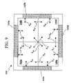
- FIG. 9is a top view of a computer chip 104 in accordance with the present invention.
- Chip 104includes processors 144 a - 144 d positioned near each other in a manner similar to that of chip 103 shown in FIG. 8 .
- control circuit 143 aextends along an outer periphery of processors 144 a and 144 b .
- control circuit 143 bextends along an outer periphery of processors 144 b and 144 d .
- Control circuit 143 cextends along an outer periphery of processors 144 a and 144 c and control circuit 143 d extends along an outer periphery of processors 144 c and 144 d.
- Signals S a1 , S a2 , S b1 , S b2 , S c1 , S c2 , S d1 , and S d2can flow between corresponding control circuits 143 a - 143 d and corresponding processors 144 a - 144 d through interconnects, similar to interconnects 138 a and 138 b , as described above, in conjunction with FIG. 6 .
- processors 144 a - 144 dare coupled together so that signals S ab , S ac , S bd , S ad , S bc , and S cd can flow therebetween as described above in conjunction with FIG. 6 above.
Landscapes
- Engineering & Computer Science (AREA)
- Manufacturing & Machinery (AREA)
- Semiconductor Memories (AREA)
- Semiconductor Integrated Circuits (AREA)
Abstract
Description
Claims (55)
Priority Applications (11)
| Application Number | Priority Date | Filing Date | Title |
|---|---|---|---|
| US11/092,521US7633162B2 (en) | 2004-06-21 | 2005-03-29 | Electronic circuit with embedded memory |
| US11/873,719US20080048327A1 (en) | 2004-06-21 | 2007-10-17 | Electronic circuit with embedded memory |
| US12/040,642US7800199B2 (en) | 2003-06-24 | 2008-02-29 | Semiconductor circuit |
| US12/397,309US7863748B2 (en) | 2003-06-24 | 2009-03-03 | Semiconductor circuit and method of fabricating the same |
| US12/470,344US8058142B2 (en) | 1996-11-04 | 2009-05-21 | Bonded semiconductor structure and method of making the same |
| US12/475,294US7799675B2 (en) | 2003-06-24 | 2009-05-29 | Bonded semiconductor structure and method of fabricating the same |
| US12/581,722US8471263B2 (en) | 2003-06-24 | 2009-10-19 | Information storage system which includes a bonded semiconductor structure |
| US12/618,542US7867822B2 (en) | 2003-06-24 | 2009-11-13 | Semiconductor memory device |
| US12/637,559US20100133695A1 (en) | 2003-01-12 | 2009-12-14 | Electronic circuit with embedded memory |
| US12/731,087US20100190334A1 (en) | 2003-06-24 | 2010-03-24 | Three-dimensional semiconductor structure and method of manufacturing the same |
| US12/874,866US8071438B2 (en) | 2003-06-24 | 2010-09-02 | Semiconductor circuit |
Applications Claiming Priority (2)
| Application Number | Priority Date | Filing Date | Title |
|---|---|---|---|
| US10/873,969US7052941B2 (en) | 2003-06-24 | 2004-06-21 | Method for making a three-dimensional integrated circuit structure |
| US11/092,521US7633162B2 (en) | 2004-06-21 | 2005-03-29 | Electronic circuit with embedded memory |
Related Parent Applications (5)
| Application Number | Title | Priority Date | Filing Date |
|---|---|---|---|
| US10/813,969Continuation-In-PartUS20050220949A1 (en) | 2004-03-31 | 2004-03-31 | Highly bioefficient isoflavone-phospholipid molecular complexes and methods of making and using the same |
| US10/873,969Continuation-In-PartUS7052941B2 (en) | 1996-11-04 | 2004-06-21 | Method for making a three-dimensional integrated circuit structure |
| US11/092,501Continuation-In-PartUS20050280155A1 (en) | 1996-11-04 | 2005-03-29 | Semiconductor bonding and layer transfer method |
| US11/092,500Continuation-In-PartUS8018058B2 (en) | 1996-11-04 | 2005-03-29 | Semiconductor memory device |
| US11/180,286Continuation-In-PartUS8779597B2 (en) | 1996-11-04 | 2005-07-12 | Semiconductor device with base support structure |
Related Child Applications (5)
| Application Number | Title | Priority Date | Filing Date |
|---|---|---|---|
| US11/092,501Continuation-In-PartUS20050280155A1 (en) | 1996-11-04 | 2005-03-29 | Semiconductor bonding and layer transfer method |
| US11/092,499Continuation-In-PartUS7470598B2 (en) | 1996-11-04 | 2005-03-29 | Semiconductor layer structure and method of making the same |
| US11/180,286Continuation-In-PartUS8779597B2 (en) | 1996-11-04 | 2005-07-12 | Semiconductor device with base support structure |
| US11/873,851Continuation-In-PartUS7718508B2 (en) | 1996-11-04 | 2007-10-17 | Semiconductor bonding and layer transfer method |
| US11/873,719DivisionUS20080048327A1 (en) | 1996-11-04 | 2007-10-17 | Electronic circuit with embedded memory |
Publications (2)
| Publication Number | Publication Date |
|---|---|
| US20050218521A1 US20050218521A1 (en) | 2005-10-06 |
| US7633162B2true US7633162B2 (en) | 2009-12-15 |
Family
ID=46304229
Family Applications (2)
| Application Number | Title | Priority Date | Filing Date |
|---|---|---|---|
| US11/092,521Expired - Fee RelatedUS7633162B2 (en) | 1996-11-04 | 2005-03-29 | Electronic circuit with embedded memory |
| US11/873,719AbandonedUS20080048327A1 (en) | 1996-11-04 | 2007-10-17 | Electronic circuit with embedded memory |
Family Applications After (1)
| Application Number | Title | Priority Date | Filing Date |
|---|---|---|---|
| US11/873,719AbandonedUS20080048327A1 (en) | 1996-11-04 | 2007-10-17 | Electronic circuit with embedded memory |
Country Status (1)
| Country | Link |
|---|---|
| US (2) | US7633162B2 (en) |
Cited By (231)
| Publication number | Priority date | Publication date | Assignee | Title |
|---|---|---|---|---|
| US20050280154A1 (en)* | 2004-06-21 | 2005-12-22 | Sang-Yun Lee | Semiconductor memory device |
| US20080078998A1 (en)* | 2006-09-28 | 2008-04-03 | Sanyo Electric Co., Ltd. | Semiconductor device |
| US20090267233A1 (en)* | 1996-11-04 | 2009-10-29 | Sang-Yun Lee | Bonded semiconductor structure and method of making the same |
| US7964916B2 (en) | 2009-04-14 | 2011-06-21 | Monolithic 3D Inc. | Method for fabrication of a semiconductor device and structure |
| US20110233676A1 (en)* | 2009-10-12 | 2011-09-29 | Monolithic 3D Inc. | Method for fabrication of a semiconductor device and structure |
| US8058137B1 (en) | 2009-04-14 | 2011-11-15 | Monolithic 3D Inc. | Method for fabrication of a semiconductor device and structure |
| US8071438B2 (en) | 2003-06-24 | 2011-12-06 | Besang Inc. | Semiconductor circuit |
| US20120082412A1 (en)* | 2006-08-31 | 2012-04-05 | Chandra Mouli | Communication Methods, Methods of Forming an Interconnect, Signal Interconnects, Integrated Circuit Structures, Circuits, and Data Apparatuses |
| US8163581B1 (en) | 2010-10-13 | 2012-04-24 | Monolith IC 3D | Semiconductor and optoelectronic devices |
| US8203148B2 (en) | 2010-10-11 | 2012-06-19 | Monolithic 3D Inc. | Semiconductor device and structure |
| US8237228B2 (en) | 2009-10-12 | 2012-08-07 | Monolithic 3D Inc. | System comprising a semiconductor device and structure |
| US8258810B2 (en) | 2010-09-30 | 2012-09-04 | Monolithic 3D Inc. | 3D semiconductor device |
| US8273610B2 (en) | 2010-11-18 | 2012-09-25 | Monolithic 3D Inc. | Method of constructing a semiconductor device and structure |
| US8283215B2 (en) | 2010-10-13 | 2012-10-09 | Monolithic 3D Inc. | Semiconductor and optoelectronic devices |
| US8298875B1 (en) | 2011-03-06 | 2012-10-30 | Monolithic 3D Inc. | Method for fabrication of a semiconductor device and structure |
| US8362800B2 (en) | 2010-10-13 | 2013-01-29 | Monolithic 3D Inc. | 3D semiconductor device including field repairable logics |
| US8362482B2 (en) | 2009-04-14 | 2013-01-29 | Monolithic 3D Inc. | Semiconductor device and structure |
| US8367524B2 (en) | 2005-03-29 | 2013-02-05 | Sang-Yun Lee | Three-dimensional integrated circuit structure |
| US8373230B1 (en) | 2010-10-13 | 2013-02-12 | Monolithic 3D Inc. | Method for fabrication of a semiconductor device and structure |
| US8373439B2 (en) | 2009-04-14 | 2013-02-12 | Monolithic 3D Inc. | 3D semiconductor device |
| US8379458B1 (en) | 2010-10-13 | 2013-02-19 | Monolithic 3D Inc. | Semiconductor device and structure |
| US8378494B2 (en) | 2009-04-14 | 2013-02-19 | Monolithic 3D Inc. | Method for fabrication of a semiconductor device and structure |
| US8378715B2 (en) | 2009-04-14 | 2013-02-19 | Monolithic 3D Inc. | Method to construct systems |
| US8384426B2 (en) | 2009-04-14 | 2013-02-26 | Monolithic 3D Inc. | Semiconductor device and structure |
| US8405420B2 (en) | 2009-04-14 | 2013-03-26 | Monolithic 3D Inc. | System comprising a semiconductor device and structure |
| US8427200B2 (en) | 2009-04-14 | 2013-04-23 | Monolithic 3D Inc. | 3D semiconductor device |
| US8440542B2 (en) | 2010-10-11 | 2013-05-14 | Monolithic 3D Inc. | Semiconductor device and structure |
| US8450804B2 (en) | 2011-03-06 | 2013-05-28 | Monolithic 3D Inc. | Semiconductor device and structure for heat removal |
| US8455978B2 (en) | 2010-05-27 | 2013-06-04 | Sang-Yun Lee | Semiconductor circuit structure and method of making the same |
| US8461035B1 (en) | 2010-09-30 | 2013-06-11 | Monolithic 3D Inc. | Method for fabrication of a semiconductor device and structure |
| US8476145B2 (en) | 2010-10-13 | 2013-07-02 | Monolithic 3D Inc. | Method of fabricating a semiconductor device and structure |
| US8492886B2 (en) | 2010-02-16 | 2013-07-23 | Monolithic 3D Inc | 3D integrated circuit with logic |
| US8536023B2 (en) | 2010-11-22 | 2013-09-17 | Monolithic 3D Inc. | Method of manufacturing a semiconductor device and structure |
| US8541819B1 (en) | 2010-12-09 | 2013-09-24 | Monolithic 3D Inc. | Semiconductor device and structure |
| US8557632B1 (en) | 2012-04-09 | 2013-10-15 | Monolithic 3D Inc. | Method for fabrication of a semiconductor device and structure |
| US8574929B1 (en) | 2012-11-16 | 2013-11-05 | Monolithic 3D Inc. | Method to form a 3D semiconductor device and structure |
| US8581349B1 (en) | 2011-05-02 | 2013-11-12 | Monolithic 3D Inc. | 3D memory semiconductor device and structure |
| US8642416B2 (en) | 2010-07-30 | 2014-02-04 | Monolithic 3D Inc. | Method of forming three dimensional integrated circuit devices using layer transfer technique |
| US8669778B1 (en) | 2009-04-14 | 2014-03-11 | Monolithic 3D Inc. | Method for design and manufacturing of a 3D semiconductor device |
| US8674470B1 (en) | 2012-12-22 | 2014-03-18 | Monolithic 3D Inc. | Semiconductor device and structure |
| US8686428B1 (en) | 2012-11-16 | 2014-04-01 | Monolithic 3D Inc. | Semiconductor device and structure |
| US8687399B2 (en) | 2011-10-02 | 2014-04-01 | Monolithic 3D Inc. | Semiconductor device and structure |
| US8723335B2 (en) | 2010-05-20 | 2014-05-13 | Sang-Yun Lee | Semiconductor circuit structure and method of forming the same using a capping layer |
| US8742476B1 (en) | 2012-11-27 | 2014-06-03 | Monolithic 3D Inc. | Semiconductor device and structure |
| US8754533B2 (en) | 2009-04-14 | 2014-06-17 | Monolithic 3D Inc. | Monolithic three-dimensional semiconductor device and structure |
| US8803206B1 (en) | 2012-12-29 | 2014-08-12 | Monolithic 3D Inc. | 3D semiconductor device and structure |
| US8901613B2 (en) | 2011-03-06 | 2014-12-02 | Monolithic 3D Inc. | Semiconductor device and structure for heat removal |
| US8902663B1 (en) | 2013-03-11 | 2014-12-02 | Monolithic 3D Inc. | Method of maintaining a memory state |
| US8975670B2 (en) | 2011-03-06 | 2015-03-10 | Monolithic 3D Inc. | Semiconductor device and structure for heat removal |
| US8994404B1 (en) | 2013-03-12 | 2015-03-31 | Monolithic 3D Inc. | Semiconductor device and structure |
| US9000557B2 (en) | 2012-03-17 | 2015-04-07 | Zvi Or-Bach | Semiconductor device and structure |
| US9012292B2 (en) | 2010-07-02 | 2015-04-21 | Sang-Yun Lee | Semiconductor memory device and method of fabricating the same |
| US9029173B2 (en) | 2011-10-18 | 2015-05-12 | Monolithic 3D Inc. | Method for fabrication of a semiconductor device and structure |
| US9099424B1 (en) | 2012-08-10 | 2015-08-04 | Monolithic 3D Inc. | Semiconductor system, device and structure with heat removal |
| US9099526B2 (en) | 2010-02-16 | 2015-08-04 | Monolithic 3D Inc. | Integrated circuit device and structure |
| US9117749B1 (en) | 2013-03-15 | 2015-08-25 | Monolithic 3D Inc. | Semiconductor device and structure |
| US9197804B1 (en) | 2011-10-14 | 2015-11-24 | Monolithic 3D Inc. | Semiconductor and optoelectronic devices |
| US9219005B2 (en) | 2011-06-28 | 2015-12-22 | Monolithic 3D Inc. | Semiconductor system and device |
| US9509313B2 (en) | 2009-04-14 | 2016-11-29 | Monolithic 3D Inc. | 3D semiconductor device |
| US9577642B2 (en) | 2009-04-14 | 2017-02-21 | Monolithic 3D Inc. | Method to form a 3D semiconductor device |
| US9711407B2 (en) | 2009-04-14 | 2017-07-18 | Monolithic 3D Inc. | Method of manufacturing a three dimensional integrated circuit by transfer of a mono-crystalline layer |
| US9871034B1 (en) | 2012-12-29 | 2018-01-16 | Monolithic 3D Inc. | Semiconductor device and structure |
| US9953925B2 (en) | 2011-06-28 | 2018-04-24 | Monolithic 3D Inc. | Semiconductor system and device |
| US10043781B2 (en) | 2009-10-12 | 2018-08-07 | Monolithic 3D Inc. | 3D semiconductor device and structure |
| US10115663B2 (en) | 2012-12-29 | 2018-10-30 | Monolithic 3D Inc. | 3D semiconductor device and structure |
| US10127344B2 (en) | 2013-04-15 | 2018-11-13 | Monolithic 3D Inc. | Automation for monolithic 3D devices |
| US10157909B2 (en) | 2009-10-12 | 2018-12-18 | Monolithic 3D Inc. | 3D semiconductor device and structure |
| US10217667B2 (en) | 2011-06-28 | 2019-02-26 | Monolithic 3D Inc. | 3D semiconductor device, fabrication method and system |
| US10224279B2 (en) | 2013-03-15 | 2019-03-05 | Monolithic 3D Inc. | Semiconductor device and structure |
| US10290682B2 (en) | 2010-10-11 | 2019-05-14 | Monolithic 3D Inc. | 3D IC semiconductor device and structure with stacked memory |
| US10297586B2 (en) | 2015-03-09 | 2019-05-21 | Monolithic 3D Inc. | Methods for processing a 3D semiconductor device |
| US10325651B2 (en) | 2013-03-11 | 2019-06-18 | Monolithic 3D Inc. | 3D semiconductor device with stacked memory |
| US10354995B2 (en) | 2009-10-12 | 2019-07-16 | Monolithic 3D Inc. | Semiconductor memory device and structure |
| US10366970B2 (en) | 2009-10-12 | 2019-07-30 | Monolithic 3D Inc. | 3D semiconductor device and structure |
| US10381328B2 (en) | 2015-04-19 | 2019-08-13 | Monolithic 3D Inc. | Semiconductor device and structure |
| US10388863B2 (en) | 2009-10-12 | 2019-08-20 | Monolithic 3D Inc. | 3D memory device and structure |
| US10388568B2 (en) | 2011-06-28 | 2019-08-20 | Monolithic 3D Inc. | 3D semiconductor device and system |
| US10418369B2 (en) | 2015-10-24 | 2019-09-17 | Monolithic 3D Inc. | Multi-level semiconductor memory device and structure |
| US10497713B2 (en) | 2010-11-18 | 2019-12-03 | Monolithic 3D Inc. | 3D semiconductor memory device and structure |
| US10515981B2 (en) | 2015-09-21 | 2019-12-24 | Monolithic 3D Inc. | Multilevel semiconductor device and structure with memory |
| US10522225B1 (en) | 2015-10-02 | 2019-12-31 | Monolithic 3D Inc. | Semiconductor device with non-volatile memory |
| US10600888B2 (en) | 2012-04-09 | 2020-03-24 | Monolithic 3D Inc. | 3D semiconductor device |
| US10600657B2 (en) | 2012-12-29 | 2020-03-24 | Monolithic 3D Inc | 3D semiconductor device and structure |
| US10651054B2 (en) | 2012-12-29 | 2020-05-12 | Monolithic 3D Inc. | 3D semiconductor device and structure |
| US10679977B2 (en) | 2010-10-13 | 2020-06-09 | Monolithic 3D Inc. | 3D microdisplay device and structure |
| US10825779B2 (en) | 2015-04-19 | 2020-11-03 | Monolithic 3D Inc. | 3D semiconductor device and structure |
| US10833108B2 (en) | 2010-10-13 | 2020-11-10 | Monolithic 3D Inc. | 3D microdisplay device and structure |
| US10840239B2 (en) | 2014-08-26 | 2020-11-17 | Monolithic 3D Inc. | 3D semiconductor device and structure |
| US10847540B2 (en) | 2015-10-24 | 2020-11-24 | Monolithic 3D Inc. | 3D semiconductor memory device and structure |
| US10892169B2 (en) | 2012-12-29 | 2021-01-12 | Monolithic 3D Inc. | 3D semiconductor device and structure |
| US10892016B1 (en) | 2019-04-08 | 2021-01-12 | Monolithic 3D Inc. | 3D memory semiconductor devices and structures |
| US10896931B1 (en) | 2010-10-11 | 2021-01-19 | Monolithic 3D Inc. | 3D semiconductor device and structure |
| US10903089B1 (en) | 2012-12-29 | 2021-01-26 | Monolithic 3D Inc. | 3D semiconductor device and structure |
| US10910364B2 (en) | 2009-10-12 | 2021-02-02 | Monolitaic 3D Inc. | 3D semiconductor device |
| US10943934B2 (en) | 2010-10-13 | 2021-03-09 | Monolithic 3D Inc. | Multilevel semiconductor device and structure |
| US10978501B1 (en) | 2010-10-13 | 2021-04-13 | Monolithic 3D Inc. | Multilevel semiconductor device and structure with waveguides |
| US10998374B1 (en) | 2010-10-13 | 2021-05-04 | Monolithic 3D Inc. | Multilevel semiconductor device and structure |
| US11004719B1 (en) | 2010-11-18 | 2021-05-11 | Monolithic 3D Inc. | Methods for producing a 3D semiconductor memory device and structure |
| US11004694B1 (en) | 2012-12-29 | 2021-05-11 | Monolithic 3D Inc. | 3D semiconductor device and structure |
| US11011507B1 (en) | 2015-04-19 | 2021-05-18 | Monolithic 3D Inc. | 3D semiconductor device and structure |
| US11018156B2 (en) | 2019-04-08 | 2021-05-25 | Monolithic 3D Inc. | 3D memory semiconductor devices and structures |
| US11018116B2 (en) | 2012-12-22 | 2021-05-25 | Monolithic 3D Inc. | Method to form a 3D semiconductor device and structure |
| US11018133B2 (en) | 2009-10-12 | 2021-05-25 | Monolithic 3D Inc. | 3D integrated circuit |
| US11018042B1 (en) | 2010-11-18 | 2021-05-25 | Monolithic 3D Inc. | 3D semiconductor memory device and structure |
| US11018191B1 (en) | 2010-10-11 | 2021-05-25 | Monolithic 3D Inc. | 3D semiconductor device and structure |
| US11024673B1 (en) | 2010-10-11 | 2021-06-01 | Monolithic 3D Inc. | 3D semiconductor device and structure |
| US11031394B1 (en) | 2014-01-28 | 2021-06-08 | Monolithic 3D Inc. | 3D semiconductor device and structure |
| US11030371B2 (en) | 2013-04-15 | 2021-06-08 | Monolithic 3D Inc. | Automation for monolithic 3D devices |
| US11031275B2 (en) | 2010-11-18 | 2021-06-08 | Monolithic 3D Inc. | 3D semiconductor device and structure with memory |
| US11043523B1 (en) | 2010-10-13 | 2021-06-22 | Monolithic 3D Inc. | Multilevel semiconductor device and structure with image sensors |
| US11056468B1 (en) | 2015-04-19 | 2021-07-06 | Monolithic 3D Inc. | 3D semiconductor device and structure |
| US11063071B1 (en) | 2010-10-13 | 2021-07-13 | Monolithic 3D Inc. | Multilevel semiconductor device and structure with waveguides |
| US11063024B1 (en) | 2012-12-22 | 2021-07-13 | Monlithic 3D Inc. | Method to form a 3D semiconductor device and structure |
| US11087995B1 (en) | 2012-12-29 | 2021-08-10 | Monolithic 3D Inc. | 3D semiconductor device and structure |
| US11088130B2 (en) | 2014-01-28 | 2021-08-10 | Monolithic 3D Inc. | 3D semiconductor device and structure |
| US11088050B2 (en) | 2012-04-09 | 2021-08-10 | Monolithic 3D Inc. | 3D semiconductor device with isolation layers |
| US11094576B1 (en) | 2010-11-18 | 2021-08-17 | Monolithic 3D Inc. | Methods for producing a 3D semiconductor memory device and structure |
| US11107721B2 (en) | 2010-11-18 | 2021-08-31 | Monolithic 3D Inc. | 3D semiconductor device and structure with NAND logic |
| US11107808B1 (en) | 2014-01-28 | 2021-08-31 | Monolithic 3D Inc. | 3D semiconductor device and structure |
| US11114427B2 (en) | 2015-11-07 | 2021-09-07 | Monolithic 3D Inc. | 3D semiconductor processor and memory device and structure |
| US11114464B2 (en) | 2015-10-24 | 2021-09-07 | Monolithic 3D Inc. | 3D semiconductor device and structure |
| US11121021B2 (en) | 2010-11-18 | 2021-09-14 | Monolithic 3D Inc. | 3D semiconductor device and structure |
| US11133344B2 (en) | 2010-10-13 | 2021-09-28 | Monolithic 3D Inc. | Multilevel semiconductor device and structure with image sensors |
| US11158652B1 (en) | 2019-04-08 | 2021-10-26 | Monolithic 3D Inc. | 3D memory semiconductor devices and structures |
| US11158674B2 (en) | 2010-10-11 | 2021-10-26 | Monolithic 3D Inc. | Method to produce a 3D semiconductor device and structure |
| US11164770B1 (en) | 2010-11-18 | 2021-11-02 | Monolithic 3D Inc. | Method for producing a 3D semiconductor memory device and structure |
| US11164898B2 (en) | 2010-10-13 | 2021-11-02 | Monolithic 3D Inc. | Multilevel semiconductor device and structure |
| US11164811B2 (en) | 2012-04-09 | 2021-11-02 | Monolithic 3D Inc. | 3D semiconductor device with isolation layers and oxide-to-oxide bonding |
| US11163112B2 (en) | 2010-10-13 | 2021-11-02 | Monolithic 3D Inc. | Multilevel semiconductor device and structure with electromagnetic modulators |
| US11177140B2 (en) | 2012-12-29 | 2021-11-16 | Monolithic 3D Inc. | 3D semiconductor device and structure |
| US11211279B2 (en) | 2010-11-18 | 2021-12-28 | Monolithic 3D Inc. | Method for processing a 3D integrated circuit and structure |
| US11217565B2 (en) | 2012-12-22 | 2022-01-04 | Monolithic 3D Inc. | Method to form a 3D semiconductor device and structure |
| US11227897B2 (en) | 2010-10-11 | 2022-01-18 | Monolithic 3D Inc. | Method for producing a 3D semiconductor memory device and structure |
| US11251149B2 (en) | 2016-10-10 | 2022-02-15 | Monolithic 3D Inc. | 3D memory device and structure |
| US11257867B1 (en) | 2010-10-11 | 2022-02-22 | Monolithic 3D Inc. | 3D semiconductor device and structure with oxide bonds |
| US11270055B1 (en) | 2013-04-15 | 2022-03-08 | Monolithic 3D Inc. | Automation for monolithic 3D devices |
| US11296106B2 (en) | 2019-04-08 | 2022-04-05 | Monolithic 3D Inc. | 3D memory semiconductor devices and structures |
| US11296115B1 (en) | 2015-10-24 | 2022-04-05 | Monolithic 3D Inc. | 3D semiconductor device and structure |
| US11309292B2 (en) | 2012-12-22 | 2022-04-19 | Monolithic 3D Inc. | 3D semiconductor device and structure with metal layers |
| US11315980B1 (en) | 2010-10-11 | 2022-04-26 | Monolithic 3D Inc. | 3D semiconductor device and structure with transistors |
| US11329059B1 (en) | 2016-10-10 | 2022-05-10 | Monolithic 3D Inc. | 3D memory devices and structures with thinned single crystal substrates |
| US11327227B2 (en) | 2010-10-13 | 2022-05-10 | Monolithic 3D Inc. | Multilevel semiconductor device and structure with electromagnetic modulators |
| US11341309B1 (en) | 2013-04-15 | 2022-05-24 | Monolithic 3D Inc. | Automation for monolithic 3D devices |
| US11355380B2 (en) | 2010-11-18 | 2022-06-07 | Monolithic 3D Inc. | Methods for producing 3D semiconductor memory device and structure utilizing alignment marks |
| US11355381B2 (en) | 2010-11-18 | 2022-06-07 | Monolithic 3D Inc. | 3D semiconductor memory device and structure |
| US11374118B2 (en) | 2009-10-12 | 2022-06-28 | Monolithic 3D Inc. | Method to form a 3D integrated circuit |
| US11398569B2 (en) | 2013-03-12 | 2022-07-26 | Monolithic 3D Inc. | 3D semiconductor device and structure |
| US11404466B2 (en) | 2010-10-13 | 2022-08-02 | Monolithic 3D Inc. | Multilevel semiconductor device and structure with image sensors |
| US11410912B2 (en) | 2012-04-09 | 2022-08-09 | Monolithic 3D Inc. | 3D semiconductor device with vias and isolation layers |
| US11430668B2 (en) | 2012-12-29 | 2022-08-30 | Monolithic 3D Inc. | 3D semiconductor device and structure with bonding |
| US11430667B2 (en) | 2012-12-29 | 2022-08-30 | Monolithic 3D Inc. | 3D semiconductor device and structure with bonding |
| US11437368B2 (en) | 2010-10-13 | 2022-09-06 | Monolithic 3D Inc. | Multilevel semiconductor device and structure with oxide bonding |
| US11443971B2 (en) | 2010-11-18 | 2022-09-13 | Monolithic 3D Inc. | 3D semiconductor device and structure with memory |
| US11469271B2 (en) | 2010-10-11 | 2022-10-11 | Monolithic 3D Inc. | Method to produce 3D semiconductor devices and structures with memory |
| US11476181B1 (en) | 2012-04-09 | 2022-10-18 | Monolithic 3D Inc. | 3D semiconductor device and structure with metal layers |
| US11482438B2 (en) | 2010-11-18 | 2022-10-25 | Monolithic 3D Inc. | Methods for producing a 3D semiconductor memory device and structure |
| US11482439B2 (en) | 2010-11-18 | 2022-10-25 | Monolithic 3D Inc. | Methods for producing a 3D semiconductor memory device comprising charge trap junction-less transistors |
| US11482440B2 (en) | 2010-12-16 | 2022-10-25 | Monolithic 3D Inc. | 3D semiconductor device and structure with a built-in test circuit for repairing faulty circuits |
| US11487928B2 (en) | 2013-04-15 | 2022-11-01 | Monolithic 3D Inc. | Automation for monolithic 3D devices |
| US11495484B2 (en) | 2010-11-18 | 2022-11-08 | Monolithic 3D Inc. | 3D semiconductor devices and structures with at least two single-crystal layers |
| US11508605B2 (en) | 2010-11-18 | 2022-11-22 | Monolithic 3D Inc. | 3D semiconductor memory device and structure |
| US11521888B2 (en) | 2010-11-18 | 2022-12-06 | Monolithic 3D Inc. | 3D semiconductor device and structure with high-k metal gate transistors |
| US11569117B2 (en) | 2010-11-18 | 2023-01-31 | Monolithic 3D Inc. | 3D semiconductor device and structure with single-crystal layers |
| US11574109B1 (en) | 2013-04-15 | 2023-02-07 | Monolithic 3D Inc | Automation methods for 3D integrated circuits and devices |
| US11594473B2 (en) | 2012-04-09 | 2023-02-28 | Monolithic 3D Inc. | 3D semiconductor device and structure with metal layers and a connective path |
| US11600667B1 (en) | 2010-10-11 | 2023-03-07 | Monolithic 3D Inc. | Method to produce 3D semiconductor devices and structures with memory |
| US11605663B2 (en) | 2010-10-13 | 2023-03-14 | Monolithic 3D Inc. | Multilevel semiconductor device and structure with image sensors and wafer bonding |
| US11610802B2 (en) | 2010-11-18 | 2023-03-21 | Monolithic 3D Inc. | Method for producing a 3D semiconductor device and structure with single crystal transistors and metal gate electrodes |
| US11615977B2 (en) | 2010-11-18 | 2023-03-28 | Monolithic 3D Inc. | 3D semiconductor memory device and structure |
| US11616004B1 (en) | 2012-04-09 | 2023-03-28 | Monolithic 3D Inc. | 3D semiconductor device and structure with metal layers and a connective path |
| US11694944B1 (en) | 2012-04-09 | 2023-07-04 | Monolithic 3D Inc. | 3D semiconductor device and structure with metal layers and a connective path |
| US11694922B2 (en) | 2010-10-13 | 2023-07-04 | Monolithic 3D Inc. | Multilevel semiconductor device and structure with oxide bonding |
| US11711928B2 (en) | 2016-10-10 | 2023-07-25 | Monolithic 3D Inc. | 3D memory devices and structures with control circuits |
| US11720736B2 (en) | 2013-04-15 | 2023-08-08 | Monolithic 3D Inc. | Automation methods for 3D integrated circuits and devices |
| US11735462B2 (en) | 2010-11-18 | 2023-08-22 | Monolithic 3D Inc. | 3D semiconductor device and structure with single-crystal layers |
| US11735501B1 (en) | 2012-04-09 | 2023-08-22 | Monolithic 3D Inc. | 3D semiconductor device and structure with metal layers and a connective path |
| US11763864B2 (en) | 2019-04-08 | 2023-09-19 | Monolithic 3D Inc. | 3D memory semiconductor devices and structures with bit-line pillars |
| US11784169B2 (en) | 2012-12-22 | 2023-10-10 | Monolithic 3D Inc. | 3D semiconductor device and structure with metal layers |
| US11784082B2 (en) | 2010-11-18 | 2023-10-10 | Monolithic 3D Inc. | 3D semiconductor device and structure with bonding |
| US11804396B2 (en) | 2010-11-18 | 2023-10-31 | Monolithic 3D Inc. | Methods for producing a 3D semiconductor device and structure with memory cells and multiple metal layers |
| US11812620B2 (en) | 2016-10-10 | 2023-11-07 | Monolithic 3D Inc. | 3D DRAM memory devices and structures with control circuits |
| US11855114B2 (en) | 2010-10-13 | 2023-12-26 | Monolithic 3D Inc. | Multilevel semiconductor device and structure with image sensors and wafer bonding |
| US11854857B1 (en) | 2010-11-18 | 2023-12-26 | Monolithic 3D Inc. | Methods for producing a 3D semiconductor device and structure with memory cells and multiple metal layers |
| US11855100B2 (en) | 2010-10-13 | 2023-12-26 | Monolithic 3D Inc. | Multilevel semiconductor device and structure with oxide bonding |
| US11862503B2 (en) | 2010-11-18 | 2024-01-02 | Monolithic 3D Inc. | Method for producing a 3D semiconductor device and structure with memory cells and multiple metal layers |
| US11869965B2 (en) | 2013-03-11 | 2024-01-09 | Monolithic 3D Inc. | 3D semiconductor device and structure with metal layers and memory cells |
| US11869915B2 (en) | 2010-10-13 | 2024-01-09 | Monolithic 3D Inc. | Multilevel semiconductor device and structure with image sensors and wafer bonding |
| US11869591B2 (en) | 2016-10-10 | 2024-01-09 | Monolithic 3D Inc. | 3D memory devices and structures with control circuits |
| US11881443B2 (en) | 2012-04-09 | 2024-01-23 | Monolithic 3D Inc. | 3D semiconductor device and structure with metal layers and a connective path |
| US11901210B2 (en) | 2010-11-18 | 2024-02-13 | Monolithic 3D Inc. | 3D semiconductor device and structure with memory |
| US11916045B2 (en) | 2012-12-22 | 2024-02-27 | Monolithic 3D Inc. | 3D semiconductor device and structure with metal layers |
| US11923374B2 (en) | 2013-03-12 | 2024-03-05 | Monolithic 3D Inc. | 3D semiconductor device and structure with metal layers |
| US11923230B1 (en) | 2010-11-18 | 2024-03-05 | Monolithic 3D Inc. | 3D semiconductor device and structure with bonding |
| US11929372B2 (en) | 2010-10-13 | 2024-03-12 | Monolithic 3D Inc. | Multilevel semiconductor device and structure with image sensors and wafer bonding |
| US11930648B1 (en) | 2016-10-10 | 2024-03-12 | Monolithic 3D Inc. | 3D memory devices and structures with metal layers |
| US11935949B1 (en) | 2013-03-11 | 2024-03-19 | Monolithic 3D Inc. | 3D semiconductor device and structure with metal layers and memory cells |
| US11937422B2 (en) | 2015-11-07 | 2024-03-19 | Monolithic 3D Inc. | Semiconductor memory device and structure |
| US11956952B2 (en) | 2015-08-23 | 2024-04-09 | Monolithic 3D Inc. | Semiconductor memory device and structure |
| US11961827B1 (en) | 2012-12-22 | 2024-04-16 | Monolithic 3D Inc. | 3D semiconductor device and structure with metal layers |
| US11967583B2 (en) | 2012-12-22 | 2024-04-23 | Monolithic 3D Inc. | 3D semiconductor device and structure with metal layers |
| US11978731B2 (en) | 2015-09-21 | 2024-05-07 | Monolithic 3D Inc. | Method to produce a multi-level semiconductor memory device and structure |
| US11984438B2 (en) | 2010-10-13 | 2024-05-14 | Monolithic 3D Inc. | Multilevel semiconductor device and structure with oxide bonding |
| US11984445B2 (en) | 2009-10-12 | 2024-05-14 | Monolithic 3D Inc. | 3D semiconductor devices and structures with metal layers |
| US11991884B1 (en) | 2015-10-24 | 2024-05-21 | Monolithic 3D Inc. | 3D semiconductor device and structure with logic and memory |
| US12016181B2 (en) | 2015-10-24 | 2024-06-18 | Monolithic 3D Inc. | 3D semiconductor device and structure with logic and memory |
| US12027518B1 (en) | 2009-10-12 | 2024-07-02 | Monolithic 3D Inc. | 3D semiconductor devices and structures with metal layers |
| US12035531B2 (en) | 2015-10-24 | 2024-07-09 | Monolithic 3D Inc. | 3D semiconductor device and structure with logic and memory |
| US12033884B2 (en) | 2010-11-18 | 2024-07-09 | Monolithic 3D Inc. | Methods for producing a 3D semiconductor device and structure with memory cells and multiple metal layers |
| US12051674B2 (en) | 2012-12-22 | 2024-07-30 | Monolithic 3D Inc. | 3D semiconductor device and structure with metal layers |
| US12068187B2 (en) | 2010-11-18 | 2024-08-20 | Monolithic 3D Inc. | 3D semiconductor device and structure with bonding and DRAM memory cells |
| US12080743B2 (en) | 2010-10-13 | 2024-09-03 | Monolithic 3D Inc. | Multilevel semiconductor device and structure with image sensors and wafer bonding |
| US12094892B2 (en) | 2010-10-13 | 2024-09-17 | Monolithic 3D Inc. | 3D micro display device and structure |
| US12094965B2 (en) | 2013-03-11 | 2024-09-17 | Monolithic 3D Inc. | 3D semiconductor device and structure with metal layers and memory cells |
| US12094829B2 (en) | 2014-01-28 | 2024-09-17 | Monolithic 3D Inc. | 3D semiconductor device and structure |
| US12100658B2 (en) | 2015-09-21 | 2024-09-24 | Monolithic 3D Inc. | Method to produce a 3D multilayer semiconductor device and structure |
| US12100611B2 (en) | 2010-11-18 | 2024-09-24 | Monolithic 3D Inc. | Methods for producing a 3D semiconductor device and structure with memory cells and multiple metal layers |
| US12100646B2 (en) | 2013-03-12 | 2024-09-24 | Monolithic 3D Inc. | 3D semiconductor device and structure with metal layers |
| US12120880B1 (en) | 2015-10-24 | 2024-10-15 | Monolithic 3D Inc. | 3D semiconductor device and structure with logic and memory |
| US12125737B1 (en) | 2010-11-18 | 2024-10-22 | Monolithic 3D Inc. | 3D semiconductor device and structure with metal layers and memory cells |
| US12136562B2 (en) | 2010-11-18 | 2024-11-05 | Monolithic 3D Inc. | 3D semiconductor device and structure with single-crystal layers |
| US12144190B2 (en) | 2010-11-18 | 2024-11-12 | Monolithic 3D Inc. | 3D semiconductor device and structure with bonding and memory cells preliminary class |
| US12154817B1 (en) | 2010-11-18 | 2024-11-26 | Monolithic 3D Inc. | Methods for producing a 3D semiconductor memory device and structure |
| US12178055B2 (en) | 2015-09-21 | 2024-12-24 | Monolithic 3D Inc. | 3D semiconductor memory devices and structures |
| US12219769B2 (en) | 2015-10-24 | 2025-02-04 | Monolithic 3D Inc. | 3D semiconductor device and structure with logic and memory |
| US12225704B2 (en) | 2016-10-10 | 2025-02-11 | Monolithic 3D Inc. | 3D memory devices and structures with memory arrays and metal layers |
| US12243765B2 (en) | 2010-11-18 | 2025-03-04 | Monolithic 3D Inc. | 3D semiconductor device and structure with metal layers and memory cells |
| US12249538B2 (en) | 2012-12-29 | 2025-03-11 | Monolithic 3D Inc. | 3D semiconductor device and structure including power distribution grids |
| US12250830B2 (en) | 2015-09-21 | 2025-03-11 | Monolithic 3D Inc. | 3D semiconductor memory devices and structures |
| US12272586B2 (en) | 2010-11-18 | 2025-04-08 | Monolithic 3D Inc. | 3D semiconductor memory device and structure with memory and metal layers |
| US12360310B2 (en) | 2010-10-13 | 2025-07-15 | Monolithic 3D Inc. | Multilevel semiconductor device and structure with oxide bonding |
| US12362219B2 (en) | 2010-11-18 | 2025-07-15 | Monolithic 3D Inc. | 3D semiconductor memory device and structure |
Families Citing this family (25)
| Publication number | Priority date | Publication date | Assignee | Title |
|---|---|---|---|---|
| US7863748B2 (en)* | 2003-06-24 | 2011-01-04 | Oh Choonsik | Semiconductor circuit and method of fabricating the same |
| US7767571B2 (en)* | 2006-10-13 | 2010-08-03 | Qimonda Ag | Method for manufacturing a structure in a semiconductor device and a structure in a semiconductor device |
| KR100948093B1 (en)* | 2007-12-21 | 2010-03-16 | 주식회사 하이닉스반도체 | Semiconductor device and manufacturing method thereof |
| US7974119B2 (en) | 2008-07-10 | 2011-07-05 | Seagate Technology Llc | Transmission gate-based spin-transfer torque memory unit |
| US7936580B2 (en) | 2008-10-20 | 2011-05-03 | Seagate Technology Llc | MRAM diode array and access method |
| US9030867B2 (en) | 2008-10-20 | 2015-05-12 | Seagate Technology Llc | Bipolar CMOS select device for resistive sense memory |
| US7936583B2 (en) | 2008-10-30 | 2011-05-03 | Seagate Technology Llc | Variable resistive memory punchthrough access method |
| US7825478B2 (en) | 2008-11-07 | 2010-11-02 | Seagate Technology Llc | Polarity dependent switch for resistive sense memory |
| US8178864B2 (en) | 2008-11-18 | 2012-05-15 | Seagate Technology Llc | Asymmetric barrier diode |
| US8203869B2 (en) | 2008-12-02 | 2012-06-19 | Seagate Technology Llc | Bit line charge accumulation sensing for resistive changing memory |
| US8159856B2 (en) | 2009-07-07 | 2012-04-17 | Seagate Technology Llc | Bipolar select device for resistive sense memory |
| US7911833B2 (en)* | 2009-07-13 | 2011-03-22 | Seagate Technology Llc | Anti-parallel diode structure and method of fabrication |
| US8183126B2 (en) | 2009-07-13 | 2012-05-22 | Seagate Technology Llc | Patterning embedded control lines for vertically stacked semiconductor elements |
| US8158964B2 (en) | 2009-07-13 | 2012-04-17 | Seagate Technology Llc | Schottky diode switch and memory units containing the same |
| US8208285B2 (en)* | 2009-07-13 | 2012-06-26 | Seagate Technology Llc | Vertical non-volatile switch with punchthrough access and method of fabrication therefor |
| TWI670711B (en) | 2010-09-14 | 2019-09-01 | 日商半導體能源研究所股份有限公司 | Memory device and semiconductor device |
| US8617952B2 (en) | 2010-09-28 | 2013-12-31 | Seagate Technology Llc | Vertical transistor with hardening implatation |
| KR101973212B1 (en)* | 2010-11-05 | 2019-04-26 | 가부시키가이샤 한도오따이 에네루기 켄큐쇼 | Semiconductor device |
| US8648426B2 (en) | 2010-12-17 | 2014-02-11 | Seagate Technology Llc | Tunneling transistors |
| KR101221445B1 (en)* | 2012-04-20 | 2013-01-11 | 한국과학기술원 | Capacitorless dynamic landom access memory and fabrication method thereof |
| WO2015195082A1 (en)* | 2014-06-16 | 2015-12-23 | Intel Corporation | Method for direct integration of memory die to logic die without use of through silicon vias (tsv) |
| CN106463534B (en)* | 2014-06-23 | 2020-12-11 | 英特尔公司 | Techniques for Forming Vertical Transistor Architectures |
| US10283411B1 (en)* | 2018-01-02 | 2019-05-07 | International Business Machines Corporation | Stacked vertical transistor device for three-dimensional monolithic integration |
| KR20250099267A (en)* | 2019-04-15 | 2025-07-01 | 양쯔 메모리 테크놀로지스 씨오., 엘티디. | Bonded semiconductor devices having processor and dynamic random-access memory and methods for forming the same |
| US20240204100A1 (en)* | 2022-12-20 | 2024-06-20 | International Business Machines Corporation | Vertical field effect transistor with self-aligned backside trench epitaxy |
Citations (9)
| Publication number | Priority date | Publication date | Assignee | Title |
|---|---|---|---|---|
| US6150214A (en)* | 1997-11-21 | 2000-11-21 | Texas Instruments Incorporated | Titanium nitride metal interconnection system and method of forming the same |
| US6229161B1 (en)* | 1998-06-05 | 2001-05-08 | Stanford University | Semiconductor capacitively-coupled NDR device and its applications in high-density high-speed memories and in power switches |
| US20020024140A1 (en)* | 2000-03-31 | 2002-02-28 | Takashi Nakajima | Semiconductor device |
| US20020125524A1 (en)* | 2000-02-03 | 2002-09-12 | Mitsubishi Denki Kabushiki Kaisha | Semiconductor device and method of manufacturing same |
| US20020153548A1 (en)* | 2000-07-31 | 2002-10-24 | Fujitsu Limited | Semiconductor device and method of manufacturing the same |
| US20040023065A1 (en)* | 2002-03-28 | 2004-02-05 | Nve Corporation | Superparamagnetic devices |
| US20040147077A1 (en)* | 1997-04-10 | 2004-07-29 | Kozo Watanabe | Semiconductor integrated circuitry and method for manufacturing the circuitry |
| US20040156233A1 (en)* | 2003-02-10 | 2004-08-12 | Arup Bhattacharyya | TFT-based random access memory cells comprising thyristors |
| US6790713B1 (en)* | 2002-09-09 | 2004-09-14 | T-Ram, Inc. | Method for making an inlayed thyristor-based device |
Family Cites Families (34)
| Publication number | Priority date | Publication date | Assignee | Title |
|---|---|---|---|---|
| KR900008647B1 (en)* | 1986-03-20 | 1990-11-26 | 후지쓰 가부시끼가이샤 | A method for manufacturing three demensional i.c. |
| US4829018A (en)* | 1986-06-27 | 1989-05-09 | Wahlstrom Sven E | Multilevel integrated circuits employing fused oxide layers |
| US4704785A (en)* | 1986-08-01 | 1987-11-10 | Texas Instruments Incorporated | Process for making a buried conductor by fusing two wafers |
| US4887134A (en)* | 1986-09-26 | 1989-12-12 | Canon Kabushiki Kaisha | Semiconductor device having a semiconductor region in which either the conduction or valence band remains flat while bandgap is continuously graded |
| JP2606857B2 (en)* | 1987-12-10 | 1997-05-07 | 株式会社日立製作所 | Method for manufacturing semiconductor memory device |
| JPH0344067A (en)* | 1989-07-11 | 1991-02-25 | Nec Corp | Laminating method of semiconductor substrate |
| JPH05198739A (en)* | 1991-09-10 | 1993-08-06 | Mitsubishi Electric Corp | Stacked semiconductor device and manufacturing method thereof |
| US5308782A (en)* | 1992-03-02 | 1994-05-03 | Motorola | Semiconductor memory device and method of formation |
| US5554870A (en)* | 1994-02-04 | 1996-09-10 | Motorola, Inc. | Integrated circuit having both vertical and horizontal devices and process for making the same |
| US5915167A (en)* | 1997-04-04 | 1999-06-22 | Elm Technology Corporation | Three dimensional structure memory |
| US6551857B2 (en)* | 1997-04-04 | 2003-04-22 | Elm Technology Corporation | Three dimensional structure integrated circuits |
| JP4032454B2 (en)* | 1997-06-27 | 2008-01-16 | ソニー株式会社 | Manufacturing method of three-dimensional circuit element |
| US6304483B1 (en)* | 1998-02-24 | 2001-10-16 | Micron Technology, Inc. | Circuits and methods for a static random access memory using vertical transistors |
| US6153495A (en)* | 1998-03-09 | 2000-11-28 | Intersil Corporation | Advanced methods for making semiconductor devices by low temperature direct bonding |
| US6128216A (en)* | 1998-05-13 | 2000-10-03 | Micron Technology Inc. | High density planar SRAM cell with merged transistors |
| US6072223A (en)* | 1998-09-02 | 2000-06-06 | Micron Technology, Inc. | Circuit and method for a memory cell using reverse base current effect |
| US6423613B1 (en)* | 1998-11-10 | 2002-07-23 | Micron Technology, Inc. | Low temperature silicon wafer bond process with bulk material bond strength |
| US6208555B1 (en)* | 1999-03-30 | 2001-03-27 | Micron Technology, Inc. | Negative resistance memory cell and method |
| US6600173B2 (en)* | 2000-08-30 | 2003-07-29 | Cornell Research Foundation, Inc. | Low temperature semiconductor layering and three-dimensional electronic circuits using the layering |
| KR100401130B1 (en)* | 2001-03-28 | 2003-10-10 | 한국전자통신연구원 | Ultra small size vertical MOSFET device and fabrication method of the MOSFET device |
| US6492662B2 (en)* | 2001-04-16 | 2002-12-10 | Ibm Corporation | T-RAM structure having dual vertical devices and method for fabricating the same |
| DE10125967C1 (en)* | 2001-05-29 | 2002-07-11 | Infineon Technologies Ag | DRAM cell arrangement used for a semiconductor storage device comprises a matrix arrangement of storage cells stacked over each other as layers, and a capacitor connected to the MOS transistor |
| JP4336758B2 (en)* | 2001-11-12 | 2009-09-30 | 日本電気株式会社 | Memory device |
| US6583452B1 (en)* | 2001-12-17 | 2003-06-24 | T-Ram, Inc. | Thyristor-based device having extended capacitive coupling |
| US6670642B2 (en)* | 2002-01-22 | 2003-12-30 | Renesas Technology Corporation. | Semiconductor memory device using vertical-channel transistors |
| US6642081B1 (en)* | 2002-04-11 | 2003-11-04 | Robert Patti | Interlocking conductor method for bonding wafers to produce stacked integrated circuits |
| US6995430B2 (en)* | 2002-06-07 | 2006-02-07 | Amberwave Systems Corporation | Strained-semiconductor-on-insulator device structures |
| US6683916B1 (en)* | 2002-07-17 | 2004-01-27 | Philippe Jean-Marc Sartori | Adaptive modulation/coding and power allocation system |
| AU2003255254A1 (en)* | 2002-08-08 | 2004-02-25 | Glenn J. Leedy | Vertical system integration |
| US7354798B2 (en)* | 2002-12-20 | 2008-04-08 | International Business Machines Corporation | Three-dimensional device fabrication method |
| JP2004253730A (en)* | 2003-02-21 | 2004-09-09 | Renesas Technology Corp | Semiconductor integrated circuit device and its manufacturing method |
| US6849481B1 (en)* | 2003-07-28 | 2005-02-01 | Chartered Semiconductor Manufacturing Ltd. | Thyristor-based SRAM and method for the fabrication thereof |
| US7304327B1 (en)* | 2003-11-12 | 2007-12-04 | T-Ram Semiconductor, Inc. | Thyristor circuit and approach for temperature stability |
| US6967149B2 (en)* | 2003-11-20 | 2005-11-22 | Hewlett-Packard Development Company, L.P. | Storage structure with cleaved layer |
- 2005
- 2005-03-29USUS11/092,521patent/US7633162B2/ennot_activeExpired - Fee Related
- 2007
- 2007-10-17USUS11/873,719patent/US20080048327A1/ennot_activeAbandoned
Patent Citations (9)
| Publication number | Priority date | Publication date | Assignee | Title |
|---|---|---|---|---|
| US20040147077A1 (en)* | 1997-04-10 | 2004-07-29 | Kozo Watanabe | Semiconductor integrated circuitry and method for manufacturing the circuitry |
| US6150214A (en)* | 1997-11-21 | 2000-11-21 | Texas Instruments Incorporated | Titanium nitride metal interconnection system and method of forming the same |
| US6229161B1 (en)* | 1998-06-05 | 2001-05-08 | Stanford University | Semiconductor capacitively-coupled NDR device and its applications in high-density high-speed memories and in power switches |
| US20020125524A1 (en)* | 2000-02-03 | 2002-09-12 | Mitsubishi Denki Kabushiki Kaisha | Semiconductor device and method of manufacturing same |
| US20020024140A1 (en)* | 2000-03-31 | 2002-02-28 | Takashi Nakajima | Semiconductor device |
| US20020153548A1 (en)* | 2000-07-31 | 2002-10-24 | Fujitsu Limited | Semiconductor device and method of manufacturing the same |
| US20040023065A1 (en)* | 2002-03-28 | 2004-02-05 | Nve Corporation | Superparamagnetic devices |
| US6790713B1 (en)* | 2002-09-09 | 2004-09-14 | T-Ram, Inc. | Method for making an inlayed thyristor-based device |
| US20040156233A1 (en)* | 2003-02-10 | 2004-08-12 | Arup Bhattacharyya | TFT-based random access memory cells comprising thyristors |
Cited By (272)
| Publication number | Priority date | Publication date | Assignee | Title |
|---|---|---|---|---|
| US20090267233A1 (en)* | 1996-11-04 | 2009-10-29 | Sang-Yun Lee | Bonded semiconductor structure and method of making the same |
| US8058142B2 (en) | 1996-11-04 | 2011-11-15 | Besang Inc. | Bonded semiconductor structure and method of making the same |
| US8071438B2 (en) | 2003-06-24 | 2011-12-06 | Besang Inc. | Semiconductor circuit |
| US20050280154A1 (en)* | 2004-06-21 | 2005-12-22 | Sang-Yun Lee | Semiconductor memory device |
| US8018058B2 (en) | 2004-06-21 | 2011-09-13 | Besang Inc. | Semiconductor memory device |
| US8367524B2 (en) | 2005-03-29 | 2013-02-05 | Sang-Yun Lee | Three-dimensional integrated circuit structure |
| US8447147B2 (en)* | 2006-08-31 | 2013-05-21 | Micron Technology, Inc. | Communication methods, methods of forming an interconnect, signal interconnects, integrated circuit structures, circuits, and data apparatuses |
| US20120082412A1 (en)* | 2006-08-31 | 2012-04-05 | Chandra Mouli | Communication Methods, Methods of Forming an Interconnect, Signal Interconnects, Integrated Circuit Structures, Circuits, and Data Apparatuses |
| US8866194B2 (en) | 2006-09-28 | 2014-10-21 | Semiconductor Components Industries, Llc | Semiconductor device |
| US20080078998A1 (en)* | 2006-09-28 | 2008-04-03 | Sanyo Electric Co., Ltd. | Semiconductor device |
| US8987079B2 (en) | 2009-04-14 | 2015-03-24 | Monolithic 3D Inc. | Method for developing a custom device |
| US9711407B2 (en) | 2009-04-14 | 2017-07-18 | Monolithic 3D Inc. | Method of manufacturing a three dimensional integrated circuit by transfer of a mono-crystalline layer |
| US8378494B2 (en) | 2009-04-14 | 2013-02-19 | Monolithic 3D Inc. | Method for fabrication of a semiconductor device and structure |
| US8669778B1 (en) | 2009-04-14 | 2014-03-11 | Monolithic 3D Inc. | Method for design and manufacturing of a 3D semiconductor device |
| US9412645B1 (en) | 2009-04-14 | 2016-08-09 | Monolithic 3D Inc. | Semiconductor devices and structures |
| US8427200B2 (en) | 2009-04-14 | 2013-04-23 | Monolithic 3D Inc. | 3D semiconductor device |
| US8405420B2 (en) | 2009-04-14 | 2013-03-26 | Monolithic 3D Inc. | System comprising a semiconductor device and structure |
| US8058137B1 (en) | 2009-04-14 | 2011-11-15 | Monolithic 3D Inc. | Method for fabrication of a semiconductor device and structure |
| US8384426B2 (en) | 2009-04-14 | 2013-02-26 | Monolithic 3D Inc. | Semiconductor device and structure |
| US9577642B2 (en) | 2009-04-14 | 2017-02-21 | Monolithic 3D Inc. | Method to form a 3D semiconductor device |
| US8378715B2 (en) | 2009-04-14 | 2013-02-19 | Monolithic 3D Inc. | Method to construct systems |
| US8362482B2 (en) | 2009-04-14 | 2013-01-29 | Monolithic 3D Inc. | Semiconductor device and structure |
| US8754533B2 (en) | 2009-04-14 | 2014-06-17 | Monolithic 3D Inc. | Monolithic three-dimensional semiconductor device and structure |
| US9509313B2 (en) | 2009-04-14 | 2016-11-29 | Monolithic 3D Inc. | 3D semiconductor device |
| US8373439B2 (en) | 2009-04-14 | 2013-02-12 | Monolithic 3D Inc. | 3D semiconductor device |
| US7964916B2 (en) | 2009-04-14 | 2011-06-21 | Monolithic 3D Inc. | Method for fabrication of a semiconductor device and structure |
| US10388863B2 (en) | 2009-10-12 | 2019-08-20 | Monolithic 3D Inc. | 3D memory device and structure |
| US8664042B2 (en) | 2009-10-12 | 2014-03-04 | Monolithic 3D Inc. | Method for fabrication of configurable systems |
| US8294159B2 (en) | 2009-10-12 | 2012-10-23 | Monolithic 3D Inc. | Method for fabrication of a semiconductor device and structure |
| US8395191B2 (en) | 2009-10-12 | 2013-03-12 | Monolithic 3D Inc. | Semiconductor device and structure |
| US10043781B2 (en) | 2009-10-12 | 2018-08-07 | Monolithic 3D Inc. | 3D semiconductor device and structure |
| US10157909B2 (en) | 2009-10-12 | 2018-12-18 | Monolithic 3D Inc. | 3D semiconductor device and structure |
| US8237228B2 (en) | 2009-10-12 | 2012-08-07 | Monolithic 3D Inc. | System comprising a semiconductor device and structure |
| US10354995B2 (en) | 2009-10-12 | 2019-07-16 | Monolithic 3D Inc. | Semiconductor memory device and structure |
| US9406670B1 (en) | 2009-10-12 | 2016-08-02 | Monolithic 3D Inc. | System comprising a semiconductor device and structure |
| US20110233676A1 (en)* | 2009-10-12 | 2011-09-29 | Monolithic 3D Inc. | Method for fabrication of a semiconductor device and structure |
| US11984445B2 (en) | 2009-10-12 | 2024-05-14 | Monolithic 3D Inc. | 3D semiconductor devices and structures with metal layers |
| US12027518B1 (en) | 2009-10-12 | 2024-07-02 | Monolithic 3D Inc. | 3D semiconductor devices and structures with metal layers |
| US11374118B2 (en) | 2009-10-12 | 2022-06-28 | Monolithic 3D Inc. | Method to form a 3D integrated circuit |
| US10910364B2 (en) | 2009-10-12 | 2021-02-02 | Monolitaic 3D Inc. | 3D semiconductor device |
| US11018133B2 (en) | 2009-10-12 | 2021-05-25 | Monolithic 3D Inc. | 3D integrated circuit |
| US20110233617A1 (en)* | 2009-10-12 | 2011-09-29 | Monolithic 3D Inc. | Method for fabrication of a semiconductor device and structure |
| US10366970B2 (en) | 2009-10-12 | 2019-07-30 | Monolithic 3D Inc. | 3D semiconductor device and structure |
| US8907442B2 (en) | 2009-10-12 | 2014-12-09 | Monolthic 3D Inc. | System comprising a semiconductor device and structure |
| US8148728B2 (en) | 2009-10-12 | 2012-04-03 | Monolithic 3D, Inc. | Method for fabrication of a semiconductor device and structure |
| US9564432B2 (en) | 2010-02-16 | 2017-02-07 | Monolithic 3D Inc. | 3D semiconductor device and structure |
| US8846463B1 (en) | 2010-02-16 | 2014-09-30 | Monolithic 3D Inc. | Method to construct a 3D semiconductor device |
| US9099526B2 (en) | 2010-02-16 | 2015-08-04 | Monolithic 3D Inc. | Integrated circuit device and structure |
| US8492886B2 (en) | 2010-02-16 | 2013-07-23 | Monolithic 3D Inc | 3D integrated circuit with logic |
| US8723335B2 (en) | 2010-05-20 | 2014-05-13 | Sang-Yun Lee | Semiconductor circuit structure and method of forming the same using a capping layer |
| US8455978B2 (en) | 2010-05-27 | 2013-06-04 | Sang-Yun Lee | Semiconductor circuit structure and method of making the same |
| US9012292B2 (en) | 2010-07-02 | 2015-04-21 | Sang-Yun Lee | Semiconductor memory device and method of fabricating the same |
| US8709880B2 (en) | 2010-07-30 | 2014-04-29 | Monolithic 3D Inc | Method for fabrication of a semiconductor device and structure |
| US8642416B2 (en) | 2010-07-30 | 2014-02-04 | Monolithic 3D Inc. | Method of forming three dimensional integrated circuit devices using layer transfer technique |
| US8912052B2 (en) | 2010-07-30 | 2014-12-16 | Monolithic 3D Inc. | Semiconductor device and structure |
| US8703597B1 (en) | 2010-09-30 | 2014-04-22 | Monolithic 3D Inc. | Method for fabrication of a semiconductor device and structure |
| US8461035B1 (en) | 2010-09-30 | 2013-06-11 | Monolithic 3D Inc. | Method for fabrication of a semiconductor device and structure |
| US8258810B2 (en) | 2010-09-30 | 2012-09-04 | Monolithic 3D Inc. | 3D semiconductor device |
| US9419031B1 (en) | 2010-10-07 | 2016-08-16 | Monolithic 3D Inc. | Semiconductor and optoelectronic devices |
| US8440542B2 (en) | 2010-10-11 | 2013-05-14 | Monolithic 3D Inc. | Semiconductor device and structure |
| US8956959B2 (en) | 2010-10-11 | 2015-02-17 | Monolithic 3D Inc. | Method of manufacturing a semiconductor device with two monocrystalline layers |
| US9818800B2 (en) | 2010-10-11 | 2017-11-14 | Monolithic 3D Inc. | Self aligned semiconductor device and structure |
| US8203148B2 (en) | 2010-10-11 | 2012-06-19 | Monolithic 3D Inc. | Semiconductor device and structure |
| US11257867B1 (en) | 2010-10-11 | 2022-02-22 | Monolithic 3D Inc. | 3D semiconductor device and structure with oxide bonds |
| US11018191B1 (en) | 2010-10-11 | 2021-05-25 | Monolithic 3D Inc. | 3D semiconductor device and structure |
| US10290682B2 (en) | 2010-10-11 | 2019-05-14 | Monolithic 3D Inc. | 3D IC semiconductor device and structure with stacked memory |
| US11600667B1 (en) | 2010-10-11 | 2023-03-07 | Monolithic 3D Inc. | Method to produce 3D semiconductor devices and structures with memory |
| US11469271B2 (en) | 2010-10-11 | 2022-10-11 | Monolithic 3D Inc. | Method to produce 3D semiconductor devices and structures with memory |
| US11158674B2 (en) | 2010-10-11 | 2021-10-26 | Monolithic 3D Inc. | Method to produce a 3D semiconductor device and structure |
| US11024673B1 (en) | 2010-10-11 | 2021-06-01 | Monolithic 3D Inc. | 3D semiconductor device and structure |
| US10896931B1 (en) | 2010-10-11 | 2021-01-19 | Monolithic 3D Inc. | 3D semiconductor device and structure |
| US11315980B1 (en) | 2010-10-11 | 2022-04-26 | Monolithic 3D Inc. | 3D semiconductor device and structure with transistors |
| US11227897B2 (en) | 2010-10-11 | 2022-01-18 | Monolithic 3D Inc. | Method for producing a 3D semiconductor memory device and structure |
| US10833108B2 (en) | 2010-10-13 | 2020-11-10 | Monolithic 3D Inc. | 3D microdisplay device and structure |
| US8379458B1 (en) | 2010-10-13 | 2013-02-19 | Monolithic 3D Inc. | Semiconductor device and structure |
| US10943934B2 (en) | 2010-10-13 | 2021-03-09 | Monolithic 3D Inc. | Multilevel semiconductor device and structure |
| US10978501B1 (en) | 2010-10-13 | 2021-04-13 | Monolithic 3D Inc. | Multilevel semiconductor device and structure with waveguides |
| US10998374B1 (en) | 2010-10-13 | 2021-05-04 | Monolithic 3D Inc. | Multilevel semiconductor device and structure |
| US12094892B2 (en) | 2010-10-13 | 2024-09-17 | Monolithic 3D Inc. | 3D micro display device and structure |
| US10679977B2 (en) | 2010-10-13 | 2020-06-09 | Monolithic 3D Inc. | 3D microdisplay device and structure |
| US12360310B2 (en) | 2010-10-13 | 2025-07-15 | Monolithic 3D Inc. | Multilevel semiconductor device and structure with oxide bonding |
| US8476145B2 (en) | 2010-10-13 | 2013-07-02 | Monolithic 3D Inc. | Method of fabricating a semiconductor device and structure |
| US11437368B2 (en) | 2010-10-13 | 2022-09-06 | Monolithic 3D Inc. | Multilevel semiconductor device and structure with oxide bonding |
| US11163112B2 (en) | 2010-10-13 | 2021-11-02 | Monolithic 3D Inc. | Multilevel semiconductor device and structure with electromagnetic modulators |
| US11327227B2 (en) | 2010-10-13 | 2022-05-10 | Monolithic 3D Inc. | Multilevel semiconductor device and structure with electromagnetic modulators |
| US11404466B2 (en) | 2010-10-13 | 2022-08-02 | Monolithic 3D Inc. | Multilevel semiconductor device and structure with image sensors |
| US11984438B2 (en) | 2010-10-13 | 2024-05-14 | Monolithic 3D Inc. | Multilevel semiconductor device and structure with oxide bonding |
| US11929372B2 (en) | 2010-10-13 | 2024-03-12 | Monolithic 3D Inc. | Multilevel semiconductor device and structure with image sensors and wafer bonding |
| US12080743B2 (en) | 2010-10-13 | 2024-09-03 | Monolithic 3D Inc. | Multilevel semiconductor device and structure with image sensors and wafer bonding |
| US8373230B1 (en) | 2010-10-13 | 2013-02-12 | Monolithic 3D Inc. | Method for fabrication of a semiconductor device and structure |
| US8362800B2 (en) | 2010-10-13 | 2013-01-29 | Monolithic 3D Inc. | 3D semiconductor device including field repairable logics |
| US11164898B2 (en) | 2010-10-13 | 2021-11-02 | Monolithic 3D Inc. | Multilevel semiconductor device and structure |
| US8283215B2 (en) | 2010-10-13 | 2012-10-09 | Monolithic 3D Inc. | Semiconductor and optoelectronic devices |
| US11374042B1 (en) | 2010-10-13 | 2022-06-28 | Monolithic 3D Inc. | 3D micro display semiconductor device and structure |
| US11063071B1 (en) | 2010-10-13 | 2021-07-13 | Monolithic 3D Inc. | Multilevel semiconductor device and structure with waveguides |
| US11869915B2 (en) | 2010-10-13 | 2024-01-09 | Monolithic 3D Inc. | Multilevel semiconductor device and structure with image sensors and wafer bonding |
| US11605663B2 (en) | 2010-10-13 | 2023-03-14 | Monolithic 3D Inc. | Multilevel semiconductor device and structure with image sensors and wafer bonding |
| US11133344B2 (en) | 2010-10-13 | 2021-09-28 | Monolithic 3D Inc. | Multilevel semiconductor device and structure with image sensors |
| US11694922B2 (en) | 2010-10-13 | 2023-07-04 | Monolithic 3D Inc. | Multilevel semiconductor device and structure with oxide bonding |
| US11855100B2 (en) | 2010-10-13 | 2023-12-26 | Monolithic 3D Inc. | Multilevel semiconductor device and structure with oxide bonding |
| US11043523B1 (en) | 2010-10-13 | 2021-06-22 | Monolithic 3D Inc. | Multilevel semiconductor device and structure with image sensors |
| US8823122B2 (en) | 2010-10-13 | 2014-09-02 | Monolithic 3D Inc. | Semiconductor and optoelectronic devices |
| US8163581B1 (en) | 2010-10-13 | 2012-04-24 | Monolith IC 3D | Semiconductor and optoelectronic devices |
| US8753913B2 (en) | 2010-10-13 | 2014-06-17 | Monolithic 3D Inc. | Method for fabricating novel semiconductor and optoelectronic devices |
| US11855114B2 (en) | 2010-10-13 | 2023-12-26 | Monolithic 3D Inc. | Multilevel semiconductor device and structure with image sensors and wafer bonding |
| US12033884B2 (en) | 2010-11-18 | 2024-07-09 | Monolithic 3D Inc. | Methods for producing a 3D semiconductor device and structure with memory cells and multiple metal layers |
| US11031275B2 (en) | 2010-11-18 | 2021-06-08 | Monolithic 3D Inc. | 3D semiconductor device and structure with memory |
| US11784082B2 (en) | 2010-11-18 | 2023-10-10 | Monolithic 3D Inc. | 3D semiconductor device and structure with bonding |
| US11854857B1 (en) | 2010-11-18 | 2023-12-26 | Monolithic 3D Inc. | Methods for producing a 3D semiconductor device and structure with memory cells and multiple metal layers |
| US11735462B2 (en) | 2010-11-18 | 2023-08-22 | Monolithic 3D Inc. | 3D semiconductor device and structure with single-crystal layers |
| US8273610B2 (en) | 2010-11-18 | 2012-09-25 | Monolithic 3D Inc. | Method of constructing a semiconductor device and structure |
| US11121021B2 (en) | 2010-11-18 | 2021-09-14 | Monolithic 3D Inc. | 3D semiconductor device and structure |
| US11862503B2 (en) | 2010-11-18 | 2024-01-02 | Monolithic 3D Inc. | Method for producing a 3D semiconductor device and structure with memory cells and multiple metal layers |
| US10497713B2 (en) | 2010-11-18 | 2019-12-03 | Monolithic 3D Inc. | 3D semiconductor memory device and structure |
| US11615977B2 (en) | 2010-11-18 | 2023-03-28 | Monolithic 3D Inc. | 3D semiconductor memory device and structure |
| US11610802B2 (en) | 2010-11-18 | 2023-03-21 | Monolithic 3D Inc. | Method for producing a 3D semiconductor device and structure with single crystal transistors and metal gate electrodes |
| US11164770B1 (en) | 2010-11-18 | 2021-11-02 | Monolithic 3D Inc. | Method for producing a 3D semiconductor memory device and structure |
| US11901210B2 (en) | 2010-11-18 | 2024-02-13 | Monolithic 3D Inc. | 3D semiconductor device and structure with memory |
| US11923230B1 (en) | 2010-11-18 | 2024-03-05 | Monolithic 3D Inc. | 3D semiconductor device and structure with bonding |
| US11211279B2 (en) | 2010-11-18 | 2021-12-28 | Monolithic 3D Inc. | Method for processing a 3D integrated circuit and structure |
| US11569117B2 (en) | 2010-11-18 | 2023-01-31 | Monolithic 3D Inc. | 3D semiconductor device and structure with single-crystal layers |
| US11107721B2 (en) | 2010-11-18 | 2021-08-31 | Monolithic 3D Inc. | 3D semiconductor device and structure with NAND logic |
| US11521888B2 (en) | 2010-11-18 | 2022-12-06 | Monolithic 3D Inc. | 3D semiconductor device and structure with high-k metal gate transistors |
| US11508605B2 (en) | 2010-11-18 | 2022-11-22 | Monolithic 3D Inc. | 3D semiconductor memory device and structure |
| US11495484B2 (en) | 2010-11-18 | 2022-11-08 | Monolithic 3D Inc. | 3D semiconductor devices and structures with at least two single-crystal layers |
| US11094576B1 (en) | 2010-11-18 | 2021-08-17 | Monolithic 3D Inc. | Methods for producing a 3D semiconductor memory device and structure |
| US9136153B2 (en) | 2010-11-18 | 2015-09-15 | Monolithic 3D Inc. | 3D semiconductor device and structure with back-bias |
| US11482439B2 (en) | 2010-11-18 | 2022-10-25 | Monolithic 3D Inc. | Methods for producing a 3D semiconductor memory device comprising charge trap junction-less transistors |
| US12068187B2 (en) | 2010-11-18 | 2024-08-20 | Monolithic 3D Inc. | 3D semiconductor device and structure with bonding and DRAM memory cells |
| US12362219B2 (en) | 2010-11-18 | 2025-07-15 | Monolithic 3D Inc. | 3D semiconductor memory device and structure |
| US11482438B2 (en) | 2010-11-18 | 2022-10-25 | Monolithic 3D Inc. | Methods for producing a 3D semiconductor memory device and structure |
| US12272586B2 (en) | 2010-11-18 | 2025-04-08 | Monolithic 3D Inc. | 3D semiconductor memory device and structure with memory and metal layers |
| US11355380B2 (en) | 2010-11-18 | 2022-06-07 | Monolithic 3D Inc. | Methods for producing 3D semiconductor memory device and structure utilizing alignment marks |
| US12243765B2 (en) | 2010-11-18 | 2025-03-04 | Monolithic 3D Inc. | 3D semiconductor device and structure with metal layers and memory cells |
| US11004719B1 (en) | 2010-11-18 | 2021-05-11 | Monolithic 3D Inc. | Methods for producing a 3D semiconductor memory device and structure |
| US11443971B2 (en) | 2010-11-18 | 2022-09-13 | Monolithic 3D Inc. | 3D semiconductor device and structure with memory |
| US12100611B2 (en) | 2010-11-18 | 2024-09-24 | Monolithic 3D Inc. | Methods for producing a 3D semiconductor device and structure with memory cells and multiple metal layers |
| US12125737B1 (en) | 2010-11-18 | 2024-10-22 | Monolithic 3D Inc. | 3D semiconductor device and structure with metal layers and memory cells |
| US11804396B2 (en) | 2010-11-18 | 2023-10-31 | Monolithic 3D Inc. | Methods for producing a 3D semiconductor device and structure with memory cells and multiple metal layers |
| US12136562B2 (en) | 2010-11-18 | 2024-11-05 | Monolithic 3D Inc. | 3D semiconductor device and structure with single-crystal layers |
| US11018042B1 (en) | 2010-11-18 | 2021-05-25 | Monolithic 3D Inc. | 3D semiconductor memory device and structure |
| US12144190B2 (en) | 2010-11-18 | 2024-11-12 | Monolithic 3D Inc. | 3D semiconductor device and structure with bonding and memory cells preliminary class |
| US12154817B1 (en) | 2010-11-18 | 2024-11-26 | Monolithic 3D Inc. | Methods for producing a 3D semiconductor memory device and structure |
| US11355381B2 (en) | 2010-11-18 | 2022-06-07 | Monolithic 3D Inc. | 3D semiconductor memory device and structure |
| US8536023B2 (en) | 2010-11-22 | 2013-09-17 | Monolithic 3D Inc. | Method of manufacturing a semiconductor device and structure |
| US8541819B1 (en) | 2010-12-09 | 2013-09-24 | Monolithic 3D Inc. | Semiconductor device and structure |
| US11482440B2 (en) | 2010-12-16 | 2022-10-25 | Monolithic 3D Inc. | 3D semiconductor device and structure with a built-in test circuit for repairing faulty circuits |
| US8450804B2 (en) | 2011-03-06 | 2013-05-28 | Monolithic 3D Inc. | Semiconductor device and structure for heat removal |
| US8975670B2 (en) | 2011-03-06 | 2015-03-10 | Monolithic 3D Inc. | Semiconductor device and structure for heat removal |
| US8901613B2 (en) | 2011-03-06 | 2014-12-02 | Monolithic 3D Inc. | Semiconductor device and structure for heat removal |
| US8298875B1 (en) | 2011-03-06 | 2012-10-30 | Monolithic 3D Inc. | Method for fabrication of a semiconductor device and structure |
| US8581349B1 (en) | 2011-05-02 | 2013-11-12 | Monolithic 3D Inc. | 3D memory semiconductor device and structure |
| US9953925B2 (en) | 2011-06-28 | 2018-04-24 | Monolithic 3D Inc. | Semiconductor system and device |
| US10217667B2 (en) | 2011-06-28 | 2019-02-26 | Monolithic 3D Inc. | 3D semiconductor device, fabrication method and system |
| US10388568B2 (en) | 2011-06-28 | 2019-08-20 | Monolithic 3D Inc. | 3D semiconductor device and system |
| US9219005B2 (en) | 2011-06-28 | 2015-12-22 | Monolithic 3D Inc. | Semiconductor system and device |
| US9030858B2 (en) | 2011-10-02 | 2015-05-12 | Monolithic 3D Inc. | Semiconductor device and structure |
| US8687399B2 (en) | 2011-10-02 | 2014-04-01 | Monolithic 3D Inc. | Semiconductor device and structure |
| US9197804B1 (en) | 2011-10-14 | 2015-11-24 | Monolithic 3D Inc. | Semiconductor and optoelectronic devices |
| US9029173B2 (en) | 2011-10-18 | 2015-05-12 | Monolithic 3D Inc. | Method for fabrication of a semiconductor device and structure |
| US9000557B2 (en) | 2012-03-17 | 2015-04-07 | Zvi Or-Bach | Semiconductor device and structure |
| US11594473B2 (en) | 2012-04-09 | 2023-02-28 | Monolithic 3D Inc. | 3D semiconductor device and structure with metal layers and a connective path |
| US11088050B2 (en) | 2012-04-09 | 2021-08-10 | Monolithic 3D Inc. | 3D semiconductor device with isolation layers |
| US8557632B1 (en) | 2012-04-09 | 2013-10-15 | Monolithic 3D Inc. | Method for fabrication of a semiconductor device and structure |
| US11881443B2 (en) | 2012-04-09 | 2024-01-23 | Monolithic 3D Inc. | 3D semiconductor device and structure with metal layers and a connective path |
| US11164811B2 (en) | 2012-04-09 | 2021-11-02 | Monolithic 3D Inc. | 3D semiconductor device with isolation layers and oxide-to-oxide bonding |
| US10600888B2 (en) | 2012-04-09 | 2020-03-24 | Monolithic 3D Inc. | 3D semiconductor device |
| US11616004B1 (en) | 2012-04-09 | 2023-03-28 | Monolithic 3D Inc. | 3D semiconductor device and structure with metal layers and a connective path |
| US11735501B1 (en) | 2012-04-09 | 2023-08-22 | Monolithic 3D Inc. | 3D semiconductor device and structure with metal layers and a connective path |
| US11476181B1 (en) | 2012-04-09 | 2022-10-18 | Monolithic 3D Inc. | 3D semiconductor device and structure with metal layers |
| US9305867B1 (en) | 2012-04-09 | 2016-04-05 | Monolithic 3D Inc. | Semiconductor devices and structures |
| US11410912B2 (en) | 2012-04-09 | 2022-08-09 | Monolithic 3D Inc. | 3D semiconductor device with vias and isolation layers |
| US8836073B1 (en) | 2012-04-09 | 2014-09-16 | Monolithic 3D Inc. | Semiconductor device and structure |
| US11694944B1 (en) | 2012-04-09 | 2023-07-04 | Monolithic 3D Inc. | 3D semiconductor device and structure with metal layers and a connective path |
| US9099424B1 (en) | 2012-08-10 | 2015-08-04 | Monolithic 3D Inc. | Semiconductor system, device and structure with heat removal |
| US8686428B1 (en) | 2012-11-16 | 2014-04-01 | Monolithic 3D Inc. | Semiconductor device and structure |
| US8574929B1 (en) | 2012-11-16 | 2013-11-05 | Monolithic 3D Inc. | Method to form a 3D semiconductor device and structure |
| US8742476B1 (en) | 2012-11-27 | 2014-06-03 | Monolithic 3D Inc. | Semiconductor device and structure |
| US11217565B2 (en) | 2012-12-22 | 2022-01-04 | Monolithic 3D Inc. | Method to form a 3D semiconductor device and structure |
| US11063024B1 (en) | 2012-12-22 | 2021-07-13 | Monlithic 3D Inc. | Method to form a 3D semiconductor device and structure |
| US11967583B2 (en) | 2012-12-22 | 2024-04-23 | Monolithic 3D Inc. | 3D semiconductor device and structure with metal layers |
| US11961827B1 (en) | 2012-12-22 | 2024-04-16 | Monolithic 3D Inc. | 3D semiconductor device and structure with metal layers |
| US11916045B2 (en) | 2012-12-22 | 2024-02-27 | Monolithic 3D Inc. | 3D semiconductor device and structure with metal layers |
| US9252134B2 (en) | 2012-12-22 | 2016-02-02 | Monolithic 3D Inc. | Semiconductor device and structure |
| US11018116B2 (en) | 2012-12-22 | 2021-05-25 | Monolithic 3D Inc. | Method to form a 3D semiconductor device and structure |
| US11784169B2 (en) | 2012-12-22 | 2023-10-10 | Monolithic 3D Inc. | 3D semiconductor device and structure with metal layers |
| US11309292B2 (en) | 2012-12-22 | 2022-04-19 | Monolithic 3D Inc. | 3D semiconductor device and structure with metal layers |
| US12051674B2 (en) | 2012-12-22 | 2024-07-30 | Monolithic 3D Inc. | 3D semiconductor device and structure with metal layers |
| US8921970B1 (en) | 2012-12-22 | 2014-12-30 | Monolithic 3D Inc | Semiconductor device and structure |
| US8674470B1 (en) | 2012-12-22 | 2014-03-18 | Monolithic 3D Inc. | Semiconductor device and structure |
| US12278216B2 (en) | 2012-12-22 | 2025-04-15 | Monolithic 3D Inc. | 3D semiconductor device and structure with metal layers |
| US11430667B2 (en) | 2012-12-29 | 2022-08-30 | Monolithic 3D Inc. | 3D semiconductor device and structure with bonding |
| US10651054B2 (en) | 2012-12-29 | 2020-05-12 | Monolithic 3D Inc. | 3D semiconductor device and structure |
| US11004694B1 (en) | 2012-12-29 | 2021-05-11 | Monolithic 3D Inc. | 3D semiconductor device and structure |
| US10115663B2 (en) | 2012-12-29 | 2018-10-30 | Monolithic 3D Inc. | 3D semiconductor device and structure |
| US10903089B1 (en) | 2012-12-29 | 2021-01-26 | Monolithic 3D Inc. | 3D semiconductor device and structure |
| US9911627B1 (en) | 2012-12-29 | 2018-03-06 | Monolithic 3D Inc. | Method of processing a semiconductor device |
| US11177140B2 (en) | 2012-12-29 | 2021-11-16 | Monolithic 3D Inc. | 3D semiconductor device and structure |
| US10892169B2 (en) | 2012-12-29 | 2021-01-12 | Monolithic 3D Inc. | 3D semiconductor device and structure |
| US12249538B2 (en) | 2012-12-29 | 2025-03-11 | Monolithic 3D Inc. | 3D semiconductor device and structure including power distribution grids |
| US9871034B1 (en) | 2012-12-29 | 2018-01-16 | Monolithic 3D Inc. | Semiconductor device and structure |
| US8803206B1 (en) | 2012-12-29 | 2014-08-12 | Monolithic 3D Inc. | 3D semiconductor device and structure |
| US9460991B1 (en) | 2012-12-29 | 2016-10-04 | Monolithic 3D Inc. | Semiconductor device and structure |
| US11430668B2 (en) | 2012-12-29 | 2022-08-30 | Monolithic 3D Inc. | 3D semiconductor device and structure with bonding |
| US9460978B1 (en) | 2012-12-29 | 2016-10-04 | Monolithic 3D Inc. | Semiconductor device and structure |
| US10600657B2 (en) | 2012-12-29 | 2020-03-24 | Monolithic 3D Inc | 3D semiconductor device and structure |
| US9385058B1 (en) | 2012-12-29 | 2016-07-05 | Monolithic 3D Inc. | Semiconductor device and structure |
| US11087995B1 (en) | 2012-12-29 | 2021-08-10 | Monolithic 3D Inc. | 3D semiconductor device and structure |
| US11004967B1 (en) | 2013-03-11 | 2021-05-11 | Monolithic 3D Inc. | 3D semiconductor device and structure with memory |
| US10325651B2 (en) | 2013-03-11 | 2019-06-18 | Monolithic 3D Inc. | 3D semiconductor device with stacked memory |
| US12094965B2 (en) | 2013-03-11 | 2024-09-17 | Monolithic 3D Inc. | 3D semiconductor device and structure with metal layers and memory cells |
| US11935949B1 (en) | 2013-03-11 | 2024-03-19 | Monolithic 3D Inc. | 3D semiconductor device and structure with metal layers and memory cells |
| US8902663B1 (en) | 2013-03-11 | 2014-12-02 | Monolithic 3D Inc. | Method of maintaining a memory state |
| US9496271B2 (en) | 2013-03-11 | 2016-11-15 | Monolithic 3D Inc. | 3DIC system with a two stable state memory and back-bias region |
| US11515413B2 (en) | 2013-03-11 | 2022-11-29 | Monolithic 3D Inc. | 3D semiconductor device and structure with memory |
| US11121246B2 (en) | 2013-03-11 | 2021-09-14 | Monolithic 3D Inc. | 3D semiconductor device and structure with memory |
| US11869965B2 (en) | 2013-03-11 | 2024-01-09 | Monolithic 3D Inc. | 3D semiconductor device and structure with metal layers and memory cells |
| US10964807B2 (en) | 2013-03-11 | 2021-03-30 | Monolithic 3D Inc. | 3D semiconductor device with memory |
| US10355121B2 (en) | 2013-03-11 | 2019-07-16 | Monolithic 3D Inc. | 3D semiconductor device with stacked memory |
| US8994404B1 (en) | 2013-03-12 | 2015-03-31 | Monolithic 3D Inc. | Semiconductor device and structure |
| US11398569B2 (en) | 2013-03-12 | 2022-07-26 | Monolithic 3D Inc. | 3D semiconductor device and structure |
| US12100646B2 (en) | 2013-03-12 | 2024-09-24 | Monolithic 3D Inc. | 3D semiconductor device and structure with metal layers |
| US11923374B2 (en) | 2013-03-12 | 2024-03-05 | Monolithic 3D Inc. | 3D semiconductor device and structure with metal layers |
| US10224279B2 (en) | 2013-03-15 | 2019-03-05 | Monolithic 3D Inc. | Semiconductor device and structure |
| US9117749B1 (en) | 2013-03-15 | 2015-08-25 | Monolithic 3D Inc. | Semiconductor device and structure |
| US11720736B2 (en) | 2013-04-15 | 2023-08-08 | Monolithic 3D Inc. | Automation methods for 3D integrated circuits and devices |
| US11574109B1 (en) | 2013-04-15 | 2023-02-07 | Monolithic 3D Inc | Automation methods for 3D integrated circuits and devices |
| US10127344B2 (en) | 2013-04-15 | 2018-11-13 | Monolithic 3D Inc. | Automation for monolithic 3D devices |
| US11487928B2 (en) | 2013-04-15 | 2022-11-01 | Monolithic 3D Inc. | Automation for monolithic 3D devices |
| US11270055B1 (en) | 2013-04-15 | 2022-03-08 | Monolithic 3D Inc. | Automation for monolithic 3D devices |
| US11341309B1 (en) | 2013-04-15 | 2022-05-24 | Monolithic 3D Inc. | Automation for monolithic 3D devices |
| US11030371B2 (en) | 2013-04-15 | 2021-06-08 | Monolithic 3D Inc. | Automation for monolithic 3D devices |
| US11107808B1 (en) | 2014-01-28 | 2021-08-31 | Monolithic 3D Inc. | 3D semiconductor device and structure |
| US12094829B2 (en) | 2014-01-28 | 2024-09-17 | Monolithic 3D Inc. | 3D semiconductor device and structure |
| US11031394B1 (en) | 2014-01-28 | 2021-06-08 | Monolithic 3D Inc. | 3D semiconductor device and structure |
| US11088130B2 (en) | 2014-01-28 | 2021-08-10 | Monolithic 3D Inc. | 3D semiconductor device and structure |
| US10840239B2 (en) | 2014-08-26 | 2020-11-17 | Monolithic 3D Inc. | 3D semiconductor device and structure |
| US10297586B2 (en) | 2015-03-09 | 2019-05-21 | Monolithic 3D Inc. | Methods for processing a 3D semiconductor device |
| US11056468B1 (en) | 2015-04-19 | 2021-07-06 | Monolithic 3D Inc. | 3D semiconductor device and structure |
| US10381328B2 (en) | 2015-04-19 | 2019-08-13 | Monolithic 3D Inc. | Semiconductor device and structure |
| US11011507B1 (en) | 2015-04-19 | 2021-05-18 | Monolithic 3D Inc. | 3D semiconductor device and structure |
| US10825779B2 (en) | 2015-04-19 | 2020-11-03 | Monolithic 3D Inc. | 3D semiconductor device and structure |
| US11956952B2 (en) | 2015-08-23 | 2024-04-09 | Monolithic 3D Inc. | Semiconductor memory device and structure |
| US10515981B2 (en) | 2015-09-21 | 2019-12-24 | Monolithic 3D Inc. | Multilevel semiconductor device and structure with memory |
| US12100658B2 (en) | 2015-09-21 | 2024-09-24 | Monolithic 3D Inc. | Method to produce a 3D multilayer semiconductor device and structure |
| US12178055B2 (en) | 2015-09-21 | 2024-12-24 | Monolithic 3D Inc. | 3D semiconductor memory devices and structures |
| US12250830B2 (en) | 2015-09-21 | 2025-03-11 | Monolithic 3D Inc. | 3D semiconductor memory devices and structures |
| US11978731B2 (en) | 2015-09-21 | 2024-05-07 | Monolithic 3D Inc. | Method to produce a multi-level semiconductor memory device and structure |
| US10522225B1 (en) | 2015-10-02 | 2019-12-31 | Monolithic 3D Inc. | Semiconductor device with non-volatile memory |
| US12035531B2 (en) | 2015-10-24 | 2024-07-09 | Monolithic 3D Inc. | 3D semiconductor device and structure with logic and memory |
| US12219769B2 (en) | 2015-10-24 | 2025-02-04 | Monolithic 3D Inc. | 3D semiconductor device and structure with logic and memory |
| US11296115B1 (en) | 2015-10-24 | 2022-04-05 | Monolithic 3D Inc. | 3D semiconductor device and structure |
| US11114464B2 (en) | 2015-10-24 | 2021-09-07 | Monolithic 3D Inc. | 3D semiconductor device and structure |
| US12016181B2 (en) | 2015-10-24 | 2024-06-18 | Monolithic 3D Inc. | 3D semiconductor device and structure with logic and memory |
| US11991884B1 (en) | 2015-10-24 | 2024-05-21 | Monolithic 3D Inc. | 3D semiconductor device and structure with logic and memory |
| US10847540B2 (en) | 2015-10-24 | 2020-11-24 | Monolithic 3D Inc. | 3D semiconductor memory device and structure |
| US12120880B1 (en) | 2015-10-24 | 2024-10-15 | Monolithic 3D Inc. | 3D semiconductor device and structure with logic and memory |
| US10418369B2 (en) | 2015-10-24 | 2019-09-17 | Monolithic 3D Inc. | Multi-level semiconductor memory device and structure |
| US11114427B2 (en) | 2015-11-07 | 2021-09-07 | Monolithic 3D Inc. | 3D semiconductor processor and memory device and structure |
| US11937422B2 (en) | 2015-11-07 | 2024-03-19 | Monolithic 3D Inc. | Semiconductor memory device and structure |
| US11930648B1 (en) | 2016-10-10 | 2024-03-12 | Monolithic 3D Inc. | 3D memory devices and structures with metal layers |
| US11251149B2 (en) | 2016-10-10 | 2022-02-15 | Monolithic 3D Inc. | 3D memory device and structure |
| US11711928B2 (en) | 2016-10-10 | 2023-07-25 | Monolithic 3D Inc. | 3D memory devices and structures with control circuits |
| US12225704B2 (en) | 2016-10-10 | 2025-02-11 | Monolithic 3D Inc. | 3D memory devices and structures with memory arrays and metal layers |
| US11869591B2 (en) | 2016-10-10 | 2024-01-09 | Monolithic 3D Inc. | 3D memory devices and structures with control circuits |
| US11329059B1 (en) | 2016-10-10 | 2022-05-10 | Monolithic 3D Inc. | 3D memory devices and structures with thinned single crystal substrates |
| US11812620B2 (en) | 2016-10-10 | 2023-11-07 | Monolithic 3D Inc. | 3D DRAM memory devices and structures with control circuits |
| US11296106B2 (en) | 2019-04-08 | 2022-04-05 | Monolithic 3D Inc. | 3D memory semiconductor devices and structures |
| US11158652B1 (en) | 2019-04-08 | 2021-10-26 | Monolithic 3D Inc. | 3D memory semiconductor devices and structures |
| US11018156B2 (en) | 2019-04-08 | 2021-05-25 | Monolithic 3D Inc. | 3D memory semiconductor devices and structures |
| US11763864B2 (en) | 2019-04-08 | 2023-09-19 | Monolithic 3D Inc. | 3D memory semiconductor devices and structures with bit-line pillars |
| US10892016B1 (en) | 2019-04-08 | 2021-01-12 | Monolithic 3D Inc. | 3D memory semiconductor devices and structures |
Also Published As
| Publication number | Publication date |
|---|---|
| US20050218521A1 (en) | 2005-10-06 |
| US20080048327A1 (en) | 2008-02-28 |
Similar Documents
| Publication | Publication Date | Title |
|---|---|---|
| US7633162B2 (en) | Electronic circuit with embedded memory | |
| US20100133695A1 (en) | Electronic circuit with embedded memory | |
| US8634234B2 (en) | Embedded magnetic random access memory (MRAM) | |
| US8582352B2 (en) | Methods and apparatus for FinFET SRAM cells | |
| US7376002B2 (en) | Semiconductor memory device | |
| US8289757B2 (en) | Embedded magnetic random access memory (MRAM) | |
| KR100753066B1 (en) | Magnetic semiconductor memory apparatus and method of manufacturing the same | |
| US7006370B1 (en) | Memory cell architecture | |
| US11749586B2 (en) | Semiconductor device including through via structure | |
| Liu et al. | CFET SRAM with double-sided interconnect design and DTCO benchmark | |
| TWI870393B (en) | Semiconductor device and method for fabricating the same | |
| US11957062B2 (en) | Memory | |
| US20120045872A1 (en) | Semiconductor Memory Device | |
| JP3853478B2 (en) | Manufacturing method of semiconductor integrated circuit device | |
| JPH04276659A (en) | Semiconductor integrated circuit device and its formation method | |
| US6951791B2 (en) | Global column select structure for accessing a memory | |
| CN108695328B (en) | Static random access memory element and method of forming the same | |
| US5307308A (en) | Semiconductor memory device comprising one or more high-resistance elements | |
| US20230065187A1 (en) | Structure and method of increasing subtractive bitline air gap height | |
| US20240387462A1 (en) | Semiconductor device and semiconductor package including the same | |
| CN119967809A (en) | Memory device and method of manufacturing the same | |
| TW202518456A (en) | Memory device and method of manufacturing the same | |
| WO2025094773A1 (en) | Memory device and semiconductor device | |
| JPH04127470A (en) | Semiconductor storage device | |
| JPH03253071A (en) | Semiconductor integrated circuit device |
Legal Events
| Date | Code | Title | Description |
|---|---|---|---|
| CC | Certificate of correction | ||
| AS | Assignment | Owner name:BESANG, INC., OREGON Free format text:ASSIGNMENT OF ASSIGNORS INTEREST;ASSIGNOR:LEE, SANG-YUN;REEL/FRAME:025695/0105 Effective date:20101215 | |
| AS | Assignment | Owner name:DAEHONG TECHNEW CORPORATION, KOREA, REPUBLIC OF Free format text:SECURITY AGREEMENT;ASSIGNOR:BESANG INC.;REEL/FRAME:030373/0668 Effective date:20130507 | |
| REMI | Maintenance fee reminder mailed | ||
| FEPP | Fee payment procedure | Free format text:PETITION RELATED TO MAINTENANCE FEES GRANTED (ORIGINAL EVENT CODE: PMFG); ENTITY STATUS OF PATENT OWNER: SMALL ENTITY Free format text:PETITION RELATED TO MAINTENANCE FEES FILED (ORIGINAL EVENT CODE: PMFP); ENTITY STATUS OF PATENT OWNER: SMALL ENTITY | |
| LAPS | Lapse for failure to pay maintenance fees | ||
| REIN | Reinstatement after maintenance fee payment confirmed | ||
| FP | Lapsed due to failure to pay maintenance fee | Effective date:20131215 | |
| FPAY | Fee payment | Year of fee payment:4 | |
| PRDP | Patent reinstated due to the acceptance of a late maintenance fee | Effective date:20140909 | |
| REMI | Maintenance fee reminder mailed | ||
| LAPS | Lapse for failure to pay maintenance fees | Free format text:PATENT EXPIRED FOR FAILURE TO PAY MAINTENANCE FEES (ORIGINAL EVENT CODE: EXP.) | |
| STCH | Information on status: patent discontinuation | Free format text:PATENT EXPIRED DUE TO NONPAYMENT OF MAINTENANCE FEES UNDER 37 CFR 1.362 | |
| FP | Lapsed due to failure to pay maintenance fee | Effective date:20171215 | |
| AS | Assignment | Owner name:BESANG INC., OREGON Free format text:RELEASE BY SECURED PARTY;ASSIGNOR:DAEHONG TECHNEW CORPORATION;REEL/FRAME:045658/0353 Effective date:20180427 |