US7630446B2 - Apparatus and method for automatic polarity swap in a communications system - Google Patents
Apparatus and method for automatic polarity swap in a communications systemDownload PDFInfo
- Publication number
- US7630446B2 US7630446B2US12/222,367US22236708AUS7630446B2US 7630446 B2US7630446 B2US 7630446B2US 22236708 AUS22236708 AUS 22236708AUS 7630446 B2US7630446 B2US 7630446B2
- Authority
- US
- United States
- Prior art keywords
- transceiver
- data
- serial
- parallel
- data word
- Prior art date
- Legal status (The legal status is an assumption and is not a legal conclusion. Google has not performed a legal analysis and makes no representation as to the accuracy of the status listed.)
- Expired - Fee Related
Links
- 238000004891communicationMethods0.000titleclaimsabstractdescription25
- 238000000034methodMethods0.000titledescription7
- 230000008878couplingEffects0.000claims2
- 238000010168coupling processMethods0.000claims2
- 238000005859coupling reactionMethods0.000claims2
- 238000012937correctionMethods0.000abstractdescription7
- 238000006243chemical reactionMethods0.000abstractdescription5
- 230000009471actionEffects0.000abstractdescription2
- 238000012360testing methodMethods0.000description19
- 239000000758substrateSubstances0.000description18
- 230000005540biological transmissionEffects0.000description9
- 239000004065semiconductorSubstances0.000description8
- 239000000872bufferSubstances0.000description4
- 230000008569processEffects0.000description3
- 238000012545processingMethods0.000description3
- 230000008901benefitEffects0.000description2
- 230000008859changeEffects0.000description2
- 235000012489doughnutsNutrition0.000description2
- 230000009977dual effectEffects0.000description2
- 238000010977unit operationMethods0.000description2
- 101001038535Pelodiscus sinensis Lysozyme CProteins0.000description1
- 238000005516engineering processMethods0.000description1
- 230000006870functionEffects0.000description1
- 230000010354integrationEffects0.000description1
Images


Classifications
- H—ELECTRICITY
- H04—ELECTRIC COMMUNICATION TECHNIQUE
- H04L—TRANSMISSION OF DIGITAL INFORMATION, e.g. TELEGRAPHIC COMMUNICATION
- H04L25/00—Baseband systems
- H04L25/02—Details ; arrangements for supplying electrical power along data transmission lines
- H04L25/0264—Arrangements for coupling to transmission lines
- H04L25/0272—Arrangements for coupling to multiple lines, e.g. for differential transmission
- H—ELECTRICITY
- H04—ELECTRIC COMMUNICATION TECHNIQUE
- H04L—TRANSMISSION OF DIGITAL INFORMATION, e.g. TELEGRAPHIC COMMUNICATION
- H04L25/00—Baseband systems
- H04L25/02—Details ; arrangements for supplying electrical power along data transmission lines
- H—ELECTRICITY
- H04—ELECTRIC COMMUNICATION TECHNIQUE
- H04L—TRANSMISSION OF DIGITAL INFORMATION, e.g. TELEGRAPHIC COMMUNICATION
- H04L25/00—Baseband systems
- H04L25/02—Details ; arrangements for supplying electrical power along data transmission lines
- H04L25/0264—Arrangements for coupling to transmission lines
- H04L25/0292—Arrangements specific to the receiver end
Definitions
- the present inventiongenerally relates to serial de-serializer integrated circuits with multiple high speed data ports, and more particularly to an automatic polarity swap to correct for any differential cross-connect at the input of one or more serial data ports.
- High speed data linkstransmit data from one location to another over transmission lines.
- These data linkscan include serial deserializer data links (i.e. SERDES) that receive data in a parallel format and convert the data to a serial format for high speed transmission.
- SERDES data linkscan be part of a backplane in a communications system (e.g. Tyco Backplane 30-inch trace).
- a multi-port Serdes transceiverincludes multiple parallel ports and serial ports, and includes the flexibility to connect any one of the parallel ports to another parallel port or to a serial port, or both. Furthermore, the multiport transceiver chip can connect any one of the serial ports to another serial port or to one of the parallel ports. The multi-port Serdes transceiver is able to operate at multiple data rates.
- the multi-port Serdes transceiveralso includes a packet bit error rate tester (BERT).
- the packet BERTgenerates and processes packet test data that can be transmitted over any of the serial ports to perform bit error testing.
- the packet BERTcan monitor (or “snoop”) between the serial ports. In other words, if data is being transmitted from one serial port to another serial port, the packet BERT can capture and store a portion of this data for bit error testing.
- the substrate layout of the multi-port Serdes transceiver chipis configured so that the parallel ports and the serial ports are on the outer perimeter of the substrate.
- a logic coreis at the center of the substrate, where the logic core operates the serial and parallel data ports, and a bus that connects the data ports.
- the buscan be described as a “ring” structure (or donut “structure”) around the logic core, and is configured between the logic core and the data ports.
- the ring structure of the busprovides efficient communication between the logic core and the various data ports.
- the Serdes transceiver described hereinis highly flexible and can be configured to provide multiple different transceiver products from enabling and disabling various serial and parallel data ports. This is accomplished using a configuration logic circuit that enables/disables these data ports. As a result, several different transceiver products, with different capabilities and price points, can be configured from a single semiconductor die.
- two or more transceivers having differential inputs and outputscan be coupled together through an interface, such as a backplane to form a communications system.
- an interfacesuch as a backplane
- the present inventionincludes an error check and correction module that detects invalid data words after parallel-to-serial conversion. More specifically, an error check determines if the parallel differential signal represents a valid data word. This can be done, for example, by storing and comparing valid data words in a memory such as RAM. If the received data word is valid, then no corrective action is taken.
- the parallel differential signalis inverted using a logic circuit, which will correct the error if it is due to cross-connection of the differential lines.
- the inversion of the parallel differential signalis implemented using an X-OR logic circuit.
- the X-OR logic circuitoperates on the parallel differential signal according to a control bit. When the control bit is set to “1”, the X-OR logic circuit will invert the signal components of the parallel differential signal.
- Other logic circuitscould also be used to perform the signal inversion.
- FIG. Iillustrates a multi-port Serdes chip according to embodiments of the present invention.
- FIG. 2further illustrates the multi-port Serdes chip including a parallel-to-serial conversion according to embodiments of the present invention.
- FIG. 3further illustrates the operation of the transceiver 100 in the routing of serial data between ports according to embodiments of the present invention.
- FIG. 4illustrates a multi-port Serdes transceiver 400 , which is one embodiment of the transceiver 100 .
- FIG. 5illustrates a substrate layout of the multi-port Serdes transceiver chip according to embodiments of the present invention.
- FIG. 6illustrates a section of the bus 106 according to embodiments of the present invention.
- FIG. 7further illustrates the bus 106 having equal length transmission lines according to embodiments of the present invention.
- FIG. 8illustrates a transceiver 800 , which one configuration of the transceiver 400 .
- FIG. 9illustrates a transceiver 900 , which is another configuration of the transceiver 400 .
- FIG. 10illustrates a transceiver 1000 , which is another configuration of the transceiver 400 .
- FIG. 11illustrates a transceiver 1100 , which is another configuration of the transceiver 400 .
- FIG. 12illustrates a transceiver 1200 , which is another configuration of the transceiver 400 .
- FIG. 13illustrates a communications system with a backplane interface.
- FIG. 14illustrates a transceiver 1400 with automatic polarity swap according to embodiments of the present invention.
- FIG. 15illustrates a flowchart that further describes automatic polarity swap according to embodiments of the present invention.
- FIG. 1illustrates a multi-port transceiver 100 according to embodiments of the present invention.
- Transceiver 100includes a plurality of serial ports 104 a - d , a plurality of parallel ports 102 a - b , and a bus 106 .
- Each of the plurality of serial ports 104is capable of transmitting and receiving data in a serial format
- each of the parallel ports 102is capable of transmitting and receiving data in a parallel format.
- the serial ports 104could be transmitting and receiving serial data with corresponding switches (e.g. MACs) 108 a - d.
- switchese.g. MACs
- the transceiver 100also includes a bus 106 that is coupled to the serial ports 104 a - d and the parallel ports 102 a and 102 b .
- the bus 106enables any serial port 104 to be connected to any other serial port 104 and to any parallel port 102 for data transmission, and vice versa. Therefore, data can be transmitted from any switch 108 to any other switch 108 , or can be transmitted and received to and from the parallel ports 102 .
- data received at the serial port 104 a from switch 108 acan be routed to the serial port 104 c by the bus 106 , for transmission to the switch 108 c .
- data from the switch 108 acan be routed to the other serial ports 104 b - d and to the parallel ports 102 a and 102 b through the bus 106 .
- FIG. 2illustrates that each serial port 104 can include a serial-to-parallel converter 202 , so that serial data processed by the port 104 can be converted to parallel data, and vice versa.
- serial data received by serial ports 104 from corresponding switches 108can be converted to parallel data and routed on the bus 106 .
- the serial-to-parallel converters 202are bi-directional, so that parallel data from the bus 106 can be converted to serial data for transmission from the serial port 104 to the corresponding switch 108 .
- the parallel data from the bus 106can also be converted to serial for transmission to the switch 108 .
- FIG. 2also illustrates the bus 106 to have a “ring structure” that enables the data to be sent from one adjacent port 104 to another adjacent port 104 .
- data from port 104 ais directly transmitted to ports 104 b and 104 c over the ring structure of the bus 106 . Therefore, data from any one port 104 can be connected to another port 104 using the bus 106 by transmitting data around the ring structure of the bus from one port 104 to another port 104 .
- the bus 106transmits data in a parallel format since it is connected to the parallel side of the serial to parallel converters 202 .
- the parallel format of the bus 106enables parallel data to be tapped out from the bus 106 at the parallel ports 102 a and 102 b .
- the ring structure of the bus 106will be further described herein.
- FIG. 3illustrates a flowchart 300 that further describes the operation of the transceiver 100 in the routing of serial data between ports.
- serial datais received at a first serial port 104 , from a switch 108 for example.
- the serial datais converted to parallel data.
- the parallel datais routed from one adjacent port 104 to another via the bus 106 until a destination port 104 is reached.
- the parallel datais converted back to serial.
- the serial datais transmitted from the serial destination port 104 , to a destination switch 108 for example.
- the ports of the transceiver 100can be configured to operate over a number of different data standards, as will be described further herein.
- the serial ports 104can transmit data to the switches 108 according to an XAUI serial protocol.
- the XAUI serial datais converted to XGMII parallel data for transmission over the parallel bus 106 , and therefore the XGMII parallel data can be tapped-out by the parallel ports 102 a and 102 b.
- FIG. 3illustrates a flowchart 300 that further describes the operation of the transceiver 100 in the routing of data between serial ports.
- serial datais received at a first serial port 104 , from a switch 108 for example.
- the serial datais converted to parallel data.
- the parallel datais routed from one adjacent port 104 to another port 104 via the bus 106 until a destination port 104 is reached.
- the parallel datais converted back to serial data.
- the serial datais transmitted from the serial destination port 104 , to a destination switch 108 for example.
- the parallel datacan be tapped, prior to being serialized, and transmitted for further processing at another destination.
- Parallel datais received at a parallel port 102 and routed to the other parallel port 102 or routed to a serial destination port 104 . If routed to a serial destination port, then the data is serialized prior to transmission.
- FIG. 4illustrates a multi-port Serdes transceiver 400 , which is one embodiment of the transceiver 100 .
- the Serdes transceiver 400includes multiple parallel ports 102 and serial ports 104 , and includes the flexibility to connect any one of the parallel ports 102 to another parallel port 102 or to a serial port 104 , or both.
- the multiport transceiver chip 400can connect any one of the serial ports 104 to another serial port 104 or to one of the parallel ports 102 .
- the Serdes transceiver chip 400includes two parallel transceiver ports 102 a,b , and four serial transceiver ports 104 a - d.
- the parallel transceiver ports 102 a,btransmit and receive data in a parallel format.
- the parallel transceiver ports 102 a,bcan be XGMII parallel ports, for example, where the XGMII transceiver protocol is known to those skilled in the arts.
- Each XGMII port 102can include 74 data pins, for example, operating at 1/10 the data rate of the serial ports 104 .
- the 74 pinscan transmit 36 data signals and receive 36 data signals, simultaneously, and 2 clock signals (1 transmit and 1 receive).
- the four serial ports 104 a - dcan be XAUI serial ports, and transmit and receive data in a serial format.
- Each serial port 104can be a quad serial port having four serial differential data lines using the XAUI protocol that is known to those skilled in the arts.
- the serial ports 104can operate at data rates of 3.125 GHz, 2.5 GHz, and 1.25 GHz.
- the transceiver chip 100is a mult-rate device.
- the XAUI data rates aboveare effectively quadrupled since there are four serial data lines in each serial port 104 . Therefore, the 2.5 GHz data rate is equivalent to a 10 GHz data rate.
- the parallel data ratescan operate at 1/10 of the data rates of the serial data.
- the serial ports 104can be further described as 10 Gigabit extension sub-letter (XGXS).
- XGXSdefines the parallel-to-serial conversion between the parallel XGMII protocol to serial XAUI protocol, according to the EEEE Std 802.3ae, the entire standard of which is incorporated herein by reference.
- the serial ports 104receive serial XAUI data and convert it to parallel XGMII data according the XGXS protocol.
- the parallel XGMII datais routed from adjacent port to adjacent port on the parallel bus 106 .
- the parallel bus 106enables data to travel between all the ports 102 and 104 . More specifically the bus 106 enables data to travel from one parallel port 102 to another parallel port 102 , and to travel from one parallel port 102 to a serial port 104 .
- Multiplexers 402connect the bus 106 to the parallel ports 102 and to the serial ports 104 .
- the serial port 104performs a parallel to serial conversion when receiving parallel data that is to be sent out serial.
- the bus 106enables data to travel from one serial port 104 to another serial port 104 , and to travel between a serial port 104 and a parallel port 102 .
- the parallel port 102enables parallel data to be tapped from the parallel bus 106 so that parallel data (e.g. XGMII data) can be transmitted from the transceiver 400 .
- parallel datae.g. XGMII data
- the multi-port Serdes transceiver 400is highly flexible in being able to connect multiple parallel ports 102 to multiple serial ports 104 , and vice versa.
- the Serdes transceiver chip 400can be implemented on a single CMOS substrate.
- the Serdes transceiver chip 400can be implemented using a low power 0.13-micron CMOS process technology, which lends itself to higher levels of integration and application.
- the transceiver 400enables dual unit operation, where one parallel port 102 is paired up with two of the serial ports 104 and the other parallel port 102 is paired up with the other two serial ports 104 .
- parallel port 102 acan be paired with serial ports 104 a and 104 b .
- the parallel port 102 bcan be paired with serial ports 104 c and 104 d .
- parallel port 102 acan be paired with either serial ports 104 a and 104 b , or serial ports 104 c and 104 d . In a backplane configuration, this provides flexibility to connect a parallel port to one or more serial ports, and with redundancy.
- the transceiver 400also includes a packet bit error rate tester (BERT) 406 .
- the packet BERT 406generates and processes packet test data that can be transmitted over any of the serial ports 104 to perform bit error testing. Any type of packet data can be generated to perform the testing and at different data rates.
- the packet BERT 406can generate packet data that can be used to test the Serdes data link.
- the packet BERT 406provides a built-in self test for the Serdes data link.
- the packet BERT 406generates test data that is sent over one or more of the serial ports 104 using the bus 106 to perform the bit error rate testing of the Serdes data link.
- the packet BERT 406can generate test data for a data link formed by enabling the serial ports 104 a and 104 b to connect the switch 108 a to the switch 108 c .
- the packet BERT 406can capture test data received over any one of the serial ports 104 or parallel ports 102 using the bus 106 for comparison with test data that was sent out. A bit error rate can then be determined based on this comparison.
- the packet BERT 406is RAM-based so that the test data is stored and compared in a RAM memory to perform the bit error rate test.
- the packet BERT 406is logic based so that the test data is generated by a logic function, and transmitted across a Serdes link. Upon receipt back, the test data is re-generated by the logic packet BERT 406 , for comparison with the original test data that was sent over the Serdes data link.
- a RAM packet BERT 406is more flexible than a logic packet BERT 406 because there is no limitation on the data that can be stored in the RAM packet BERT 406 . However, a logic packet BERT 406 is more efficient in terms of substrate area because a RAM occupies more area than a logic circuit.
- the packet BERT 406can monitor (or “snoop”) between the serial ports 104 . In other words, if data is being transmitted from one serial port 104 to another serial port 104 , the packet BERT 406 can capture and store a portion of this data for bit error testing. In one embodiment, the packet BERT 406 “blindly” captures data being sent from one serial port 104 to another serial port 104 . In another embodiment, the packet BERT 406 starts capturing data after a particular byte of data is transmitted. In another embodiment, the packet BERT 406 starts capturing data after an error event occurs. The packet BERT 406 is further described in U.S. patent application Ser. No. 10/681,244, filed on Oct. 9, 2003, and incorporated by reference herein in its entirety.
- the Serdes transceiver chip 400also includes the ability to include other optional logic blocks 408 that are not necessary for the operation of the Serdes transceiver.
- the logic blocks 408could be customer driven logic blocks or some other type of logic block.
- These optional logic blocks 408can transmit and receive data over the serial ports 104 or parallel ports 102 using the bus 106 .
- the packet BERT 406 and the optional blocks 408connect to the bus 106 using the multiplexers 404 .
- the Serdes transceiver chip 400also includes a management interface 412 that enables the configuration of the portions (parallel ports 102 , series port 104 , packet BERT 406 , and optional logic blocks 408 ) of the transceiver chip 100 .
- the management interface 412includes two pads 414 that enable two different management chips to program and control the portions of the transceiver chip 400 using MDIOs blocks 416 .
- one management chip connected to pad 414 acould control the parallel port 102 a and the serial ports 104 a and 104 b
- another management chip connected to pad 414 bcould control the parallel port 102 b and the serial ports 104 c and 104 d .
- the management interface 412is configured to be compatible with both IEEE Std.
- one management pad 414 a and MDIO block 416 acan be programmed to be responsive to clause 45 electricals and protocol, and the other management pad 414 b and MDIO block 416 b could be responsive to clause 22 electricals and protocol.
- the management pads 414 and MDIO blockscan mix and match clause 22 and clause 45 electrical and protocols.
- management pad 414 a and MDIO block 416 acan be responsive to clause 22 electricals and clause 45 protocols, and vice versa. Similar mix and match can be done for the management pad 414 b and the MDIO block 416 b .
- the management data padsare further described in U.S. patent application Ser. No.
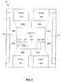
- FIG. 5illustrates the substrate layout 500 for the Serdes transceiver 400 according to embodiments of the invention.
- the substrate layout 500is configured to minimize the substrate area of the transceiver 400 , and efficiently provide the port interconnections described above.
- the substrate layout 500is configured so that the parallel ports 102 a,b and the serial ports 104 a - d are on the outer perimeter of the substrate 200 , as shown.
- the serial ports 104 a and 104 bare on a first side of the substrate layout 500 and the serial ports 104 c and 104 d are on a second side of the substrate layout 500 .
- the parallel port 102 ais on a third side of the substrate layout 500 .
- the parallel port 102 bis on a fourth side of the substrate layout 500 .
- a logic core 502is at the center of the substrate 500 , where the logic core 502 operates the bus 106 and the serial 104 and parallel 102 data ports.
- the management interface 412 , the packet BERT 406 , and the optional logic blocks 408 a - care adjacent to the logic core 502 as shown.
- the bus 106can be described as a “ring” structure (or donut “structure”) around the logic core 502 , and is placed in between the logic core 502 and the data ports 102 and 104 that occupy the parameter of the substrate layout 500 .
- the ring structure of the bus 106also provides efficient communication between the logic core 502 and the various data ports 102 and 104 .
- the ring structure of the bus 106also provides efficient communication between the management interface 412 , the packet BERT 406 , the optional logic blocks 408 , and the various data ports 102 and 104 .
- the bus 106is illustrated as 8 sections 106 a - 106 g for ease of illustration. Each section provides an interface to the respective data ports 102 or 104 that are adjacent to the respective sections.
- FIG. 6represents one of the 8 sections 106 a - 106 g of the bus 106 according to embodiments of the present invention.
- Each section of the bus 106can be represented as two paths 608 and 610 .
- Dataenters the bus 106 through a buffer 602 and proceeds to its destination along the path 608 and through the buffers 604 .
- Datapasses from one section to another section of the bus 106 using the path 610 and passing through the buffers 612 .
- the mux 606represents data passing from the bus 106 to a functional block, such as a data port 102 , 104 or the packet BERT 406 .
- the actual wires and buffers on the bus 106are matched to minimize signal distortion.
- the data wires in the bus 106are deposited on the substrate 500 in a particular fashion. Namely, a power or ground is placed between adjacent (or near by) data wires. Furthermore, adjacent data wires on the bus 106 are placed on two separate layers. Therefore, a power or ground will be above or below a data wire, and adjacent to a data wire. Therefore, two nearby data wires will not be located directly adjacent one another, but instead will be positioned diagonal to each other, thereby reducing cross talk.
- the parallel bus 106is further described in U.S. patent application Ser. No. 10/695,458, titled “Cross-Linked Multiplexer Bus”, filed Oct. 29 2003, which is incorporated by reference herein in its entirety.
- the multi-port Serdes transceiver 400supports multiple different data protocols at the pads including XGMII, TBI, RTBI, HSTL, SSTL, or LVTTL protocols, and others.
- FIG. 7further illustrates an example layout of the bus 106 .
- the wires 702 between data ports 102 , 104are configured to have the same path lengths so as to minimize signal distortion.
- wires 702 a - dare deposited so as to have the same path length so as to reduce signal distortion.
- the multi-port Serdes transceiver 400includes the ability to change the timing of the data ports 102 and 104 . This includes the ability to change the timing between the data and clock signals. In other words, the registers in the data ports 102 and 104 can be re-programmed to operate at different timing protocols.
- the Serdes transceiver 400is highly flexible and can be configured to provide multiple different transceivers by enabling and disabling various serial and parallel data ports. This is accomplished using a configuration logic circuit 418 that controls the registers and timing of the data ports 102 and 104 , and also enables/disables these data ports. As a result, several different transceiver products can be configured from a single semiconductor die that is manufactured with the 4 serial data ports and 2 parallel data ports. For instance, FIG. 1 illustrates an embodiment, where all four serial ports 104 and both parallel ports 102 are enabled and accessible to exchange data.
- the transceiver 400represents the maximum capability that can be achieved from the 4 serial and two parallel data ports. Other specific examples are discussed below, but the invention is not limited to these examples.
- FIG. 8illustrates a transceiver 800 having 4 serial XGXS data ports 104 .
- the two parallel ports 102have been disabled using configuration logic 418 and/or by not bonding the parallel ports to the output pins of the semiconductor package.
- the transceiver 800enables any of the switches 108 to exchange data with any of the other switches 108 .
- FIG. 9illustrates a transceiver 900 having 2 serial XGXS data ports 104 a and 104 b and two XGMII parallel data ports 102 a and 102 b .
- the other two serial data ports 104 c and 104 dhave been disabled using configuration logic 418 and/or by not bonding the ports to the output pins of the semiconductor package.
- the transceiver 900enables the switch 108 a to exchange data with the switch 108 b , and allows the parallel XGMII data to be tapped from the parallel bus 106 using the parallel XGMII data ports 102 a 102 b.
- the timing of the serial and parallel portsis varied to provide another transceiver product.
- the two XGXS serial portscan be configured as 8 Serdes ports that operate at a slower data rate than the XGXS data ports.
- the two XGMII parallel data portscan be configured as 8 TBI data ports that also operate at a slower data rate.
- the timing of the data portscan be revised and reconfigured for each of the transceiver configurations shown herein.
- FIG. 10illustrates a transceiver 1000 having 2 serial XGXS data ports 104 a and 104 b and only one XGMII parallel data port 102 a .
- the other two serial data ports 104 c and 104 d and the parallel port 102 bhave been disabled using configuration logic 418 and/or by not bonding the ports to the output pins of the semiconductor package.
- the transceiver 1000enables the switch 108 a to exchange data with the switch 108 b , and allows the parallel XGMII data to be tapped from the parallel bus 106 using the parallel XGMII data port 102 a.
- FIG. 11illustrates a transceiver 1100 having 2 serial XGXS data ports 104 a and 104 c and no XGMII parallel data port 102 a .
- the other two serial data ports 104 c and 104 d and the parallel ports 102have been disabled using configuration logic 418 and/or by not bonding the disabled ports to the output pins of the semiconductor package.
- the transceiver 1100enables the switch 108 a to exchange data with the switch 108 c.
- FIG. 12illustrates a transceiver 1200 having 3 serial XGXS data ports 104 a , 104 b , and 104 d and one XGMII parallel data port 102 a .
- the other serial data ports 104 c and the parallel port 102 ahave been disabled using configuration logic 418 and/or by not bonding the disabled ports to the output pins of the semiconductor package.
- the transceiver 1200enables the switches 108 a , 108 b , and 108 d to exchange data with each other.
- the base transceiver 400is highly flexible and enables multiple transceiver products, with different capabilities and price points, to be configured and sold from the base semiconductor die.
- FIG. 13illustrates a communications system 1300 having a first Serdes transceiver 100 a that communicates data with a second Serdes transceiver 100 b through an interface 1303 , that may be a backplane for example.
- the Serdes transceivers 100 a and 100 bcan be any type of the transceivers discussed herein, or any other type of transceiver.
- the Serdes transceiver 100 acan be represented as having a differential input 1301 p and 1301 n and a differential output 1302 p and 1302 n .
- the Serdes transceiver 100 bcan be described as having a differential input 1304 p and 1304 n , and a differential output 1306 p and 1306 n.
- the differential output 1302 of the transceiver 100 acan be mistakenly cross-connected with the differential input 1304 of the Serdes transceiver 100 b .
- the 1302 n output of the transceiver 100 acan be mistakenly connected to the 1304 p input of the transceiver 100 b .
- the 1302 p output of the transceiver 100 acan be mistaken connected to the 1304 n input of the transceiver 100 a .
- the result of such a cross-connectionis that invalid data words are received at the Serdes transceiver 100 b , which causes an increase in the bit error rate (BER).
- BERbit error rate
- FIG. 14illustrates an apparatus and method of automatic polarity swap to address the cross-connection problem discussed with reference to FIG. 13 .
- FIG. 14illustrates a transceiver 1400 having an error check and correction module 1401 .
- the error check and correction module 1401includes an error check 1402 and a exclusive OR (X-OR) 1404 .
- the error check and correction module 1401is coupled to the output of the serial-to-parallel converter 202 and checks the digital output of the serial-to-parallel converter 202 to determine if it is a valid digital word. If it is not a valid digital word, then the module 1401 performs an automatic polarity flip of the digital word.
- the error check and correction module 1401includes an error check 1402 at the output of the parallel-to-serial converter 202 a .
- the error check module 1402examines the digital word at the output of the parallel-to-serial converter 1402 and determines if it is a valid digital word within the context of the communications system 1300 .
- the error check module 1402can include a RAM memory that stores the possible digital word combinations for comparison with the digital word output of the serial-to-parallel converter 202 . If the digital word output of the serial-to-parallel converter 202 a does not match any one of the possible combinations, then the digital word output of the serial-to-parallel converter is not a valid digital word.
- the interface 1303is cross-connected as discussed above. If this is so, then flipping the polarity of the bits that make up the digital word, will convert the invalid digital word to a valid digital word. This can be accomplished using an exclusive-OR gate 1404 .
- the error check module 1402detects an invalid digital word, then the error check module 1402 sends a control bit logic “1” to the exclusive-OR 1404 , which causes the exclusive OR to invert the digital output from the serial-to-parallel converter, and generate a inverted digital word 1405 .
- the logic state of each portion (both p and n) of the differential lineis inverted from 0 to 1, or 1 to 0. If the error was introduced by the cross-connection, then the inverted digital word 1405 will be a valid digital word.
- the error check module 1402outputs a control bit “0” when it determines that the digital word at the output of the serial-to-parallel converter is a valid digital word. A control bit “0” does not invert the digital word, so that the digital word passes unchanged for further processing.
- the error check and correction module 1401can be implemented using other configurations as will be understood by those skilled in the arts based on the discussion given herein. For instance, a logic circuit other than an X-OR can be used to flip the polarity of the digital word if it is invalid.
- An advantage of implementing the automatic polarity swapis that cross-connect errors are rectified quickly and easily, without having to re-wire or re-configure any hardware.
- the polarity swapcan be implemented on the transmit side or the receive side.
- the receive implementationis shown in FIG. 14 .
- the transmit implementationwill be apparent based the description related to FIG. 14 .
- FIG. 15illustrates a flowchart 1500 that further describes an automatic polarity swap according to embodiments of the present invention.
- step 1502a serial differential signal is received.
- step 1504the serial differential signal is converted to a parallel differential data word.
- the parallel differential data wordis examined to determined if it is a valid data word for the corresponding communications system. For instance, the parallel differential data word can be compared with valid data words that are stored in a RAM. If the parallel differential data word is valid, then it is passed unmodified for further processing. For example, a valid data word can be re-serialized and transmitted to a destination switch or MAC.
- the parallel differential data wordis inverted if the parallel differential data word is found to be invalid in step 1506 .
- the differential data wordincludes a first component and a second component (i.e. positive component and a negative component), and the first component and the second component are both inverted so that a “0” becomes a “1”, and a “1” becomes a “0”.
- a logic circuitsuch as the X-OR 1404 ) can be used to invert the parallel data word is if it is invalid.
- the inverted parallel data wordcan be re-examined to determine if it is now a valid data word, and if so the inverted parallel data word can be further processed.
- the inverted parallel data wordcan be serialized and retransmitted to a destination switch, or MAC.
Landscapes
- Engineering & Computer Science (AREA)
- Power Engineering (AREA)
- Computer Networks & Wireless Communication (AREA)
- Signal Processing (AREA)
- Information Transfer Systems (AREA)
Abstract
Description
Claims (16)
Priority Applications (1)
| Application Number | Priority Date | Filing Date | Title |
|---|---|---|---|
| US12/222,367US7630446B2 (en) | 2003-10-29 | 2008-08-07 | Apparatus and method for automatic polarity swap in a communications system |
Applications Claiming Priority (2)
| Application Number | Priority Date | Filing Date | Title |
|---|---|---|---|
| US10/694,945US7430240B2 (en) | 2003-10-29 | 2003-10-29 | Apparatus and method for automatic polarity swap in a communications system |
| US12/222,367US7630446B2 (en) | 2003-10-29 | 2008-08-07 | Apparatus and method for automatic polarity swap in a communications system |
Related Parent Applications (1)
| Application Number | Title | Priority Date | Filing Date |
|---|---|---|---|
| US10/694,945ContinuationUS7430240B2 (en) | 2003-10-29 | 2003-10-29 | Apparatus and method for automatic polarity swap in a communications system |
Publications (2)
| Publication Number | Publication Date |
|---|---|
| US20080304579A1 US20080304579A1 (en) | 2008-12-11 |
| US7630446B2true US7630446B2 (en) | 2009-12-08 |
Family
ID=34549962
Family Applications (2)
| Application Number | Title | Priority Date | Filing Date |
|---|---|---|---|
| US10/694,945Active2025-10-24US7430240B2 (en) | 2003-10-29 | 2003-10-29 | Apparatus and method for automatic polarity swap in a communications system |
| US12/222,367Expired - Fee RelatedUS7630446B2 (en) | 2003-10-29 | 2008-08-07 | Apparatus and method for automatic polarity swap in a communications system |
Family Applications Before (1)
| Application Number | Title | Priority Date | Filing Date |
|---|---|---|---|
| US10/694,945Active2025-10-24US7430240B2 (en) | 2003-10-29 | 2003-10-29 | Apparatus and method for automatic polarity swap in a communications system |
Country Status (1)
| Country | Link |
|---|---|
| US (2) | US7430240B2 (en) |
Cited By (1)
| Publication number | Priority date | Publication date | Assignee | Title |
|---|---|---|---|---|
| US20120243622A1 (en)* | 2011-03-23 | 2012-09-27 | Broadcom Corporation | Method and apparatus for improving the error rate of a serial/de-serial backplane connection |
Families Citing this family (11)
| Publication number | Priority date | Publication date | Assignee | Title |
|---|---|---|---|---|
| US7430240B2 (en)* | 2003-10-29 | 2008-09-30 | Broadcom Corporation | Apparatus and method for automatic polarity swap in a communications system |
| US20050289435A1 (en)* | 2004-06-29 | 2005-12-29 | Mulla Dean A | Fast approximate DINV calculation in parallel with coupled ECC generation or correction |
| US20060080632A1 (en)* | 2004-09-30 | 2006-04-13 | Mathstar, Inc. | Integrated circuit layout having rectilinear structure of objects |
| WO2006039522A2 (en)* | 2004-09-30 | 2006-04-13 | Boston Scientific Scimed, Inc. | Adapter for use with digital imaging medical device |
| US20070247189A1 (en)* | 2005-01-25 | 2007-10-25 | Mathstar | Field programmable semiconductor object array integrated circuit |
| JP4809439B2 (en)* | 2006-09-29 | 2011-11-09 | 富士通株式会社 | Integrated circuit |
| US20090144595A1 (en)* | 2007-11-30 | 2009-06-04 | Mathstar, Inc. | Built-in self-testing (bist) of field programmable object arrays |
| WO2017151141A1 (en)* | 2016-03-04 | 2017-09-08 | Hewlett Packard Enterprise Development Lp | Matching data i/o types on backplane systems |
| CN106227155B (en)* | 2016-07-20 | 2019-03-12 | 上海宇航系统工程研究所 | A kind of satellite antenna servo controller Multi-serial port real-time communication control system and method |
| US10721473B2 (en)* | 2016-07-25 | 2020-07-21 | Honeywell International Inc. | Systems and methods for adjusting the frame rate of transmitted video based on the level of motion in the video |
| US12204423B1 (en)* | 2023-04-21 | 2025-01-21 | Cadence Design Systems, Inc. | System and method for verifying a cross-connection of lanes in a multi-lane environment using a single testbench |
Citations (36)
| Publication number | Priority date | Publication date | Assignee | Title |
|---|---|---|---|---|
| US4627070A (en) | 1981-09-16 | 1986-12-02 | Fmc Corporation | Asynchronous data bus system |
| US4833695A (en) | 1987-09-08 | 1989-05-23 | Tektronix, Inc. | Apparatus for skew compensating signals |
| US4833605A (en) | 1984-08-16 | 1989-05-23 | Mitsubishi Denki Kabushiki Kaisha | Cascaded information processing module having operation unit, parallel port, and serial port for concurrent data transfer and data processing |
| US4967201A (en) | 1987-10-22 | 1990-10-30 | Westinghouse Electric Corp. | Multi-layer single substrate microwave transmit/receive module |
| US5726991A (en) | 1993-06-07 | 1998-03-10 | At&T Global Information Solutions Company | Integral bit error rate test system for serial data communication links |
| US5793990A (en) | 1993-06-11 | 1998-08-11 | Vlsi Technology, Inc. | Multiplex address/data bus with multiplex system controller and method therefor |
| US5903613A (en) | 1996-01-23 | 1999-05-11 | Seiko Epson Corporation | Data reception device, data reception method and electronic equipment |
| US5933021A (en) | 1996-06-18 | 1999-08-03 | Sun Microsystems, Inc | Noise suppression method and circuits for sensitive circuits |
| US6081570A (en) | 1997-09-02 | 2000-06-27 | The United States Of America As Represented By The Administrator Of The National Aeronautics And Space Administration | Parallel integrated frame synchronizer chip |
| US6137734A (en) | 1999-03-30 | 2000-10-24 | Lsi Logic Corporation | Computer memory interface having a memory controller that automatically adjusts the timing of memory interface signals |
| US6140956A (en) | 1997-06-25 | 2000-10-31 | Cellutrac, Inc. | Vehicle tracking and security system incorporating simultaneous voice and data communication |
| US6259693B1 (en) | 1997-08-28 | 2001-07-10 | Ascend Communications, Inc. | Cell combination to utilize available switch bandwidth |
| US20010012288A1 (en) | 1999-07-14 | 2001-08-09 | Shaohua Yu | Data transmission apparatus and method for transmitting data between physical layer side device and network layer device |
| US20010015664A1 (en) | 2000-02-23 | 2001-08-23 | Fujitsu Limited | Delay time adjusting method of delaying a phase of an output signal until a phase difference between an input signal and the output signal becomes an integral number of periods other than zero |
| US20010017595A1 (en) | 1998-05-27 | 2001-08-30 | Richard Cliff | Programmable voltage regulator |
| US20010021953A1 (en) | 2000-01-14 | 2001-09-13 | Katsuya Nakashima | Data processing circuit |
| US6317804B1 (en) | 1998-11-30 | 2001-11-13 | Philips Semiconductors Inc. | Concurrent serial interconnect for integrating functional blocks in an integrated circuit device |
| US20020054569A1 (en) | 2000-11-07 | 2002-05-09 | Casio Computer Co., Ltd. | Data communication terminal |
| US6438717B1 (en) | 1999-05-26 | 2002-08-20 | 3Com Corporation | High speed parallel bit error rate tester |
| US6483849B1 (en) | 1998-04-17 | 2002-11-19 | Advanced Micro Devices, Inc. | Network transceiver having a LED interface operable in parallel and serial modes |
| US20030009307A1 (en) | 2001-01-18 | 2003-01-09 | Mejia Robert G. | Digital data pattern detection methods and arrangements |
| US20030048781A1 (en) | 1999-12-02 | 2003-03-13 | Worldcom, Inc. | Method and system for implementing an improved universal packet switching capability in a data switch |
| US20030057932A1 (en) | 2001-09-12 | 2003-03-27 | Jui-Feng Chang | Method for detecting connection polarity of network transmission lines and associated detection circuit |
| US20030120791A1 (en) | 2001-12-20 | 2003-06-26 | Weber David M. | Multi-thread, multi-speed, multi-mode interconnect protocol controller |
| US20030172332A1 (en) | 2002-03-08 | 2003-09-11 | Jeffrey R. Rearick | Systems and methods for facilitating testing of pad drivers of integrated circuits |
| US20040083077A1 (en) | 2002-10-29 | 2004-04-29 | Broadcom Corporation | Integrated packet bit error rate tester for 10G SERDES |
| US20040153945A1 (en) | 2002-11-22 | 2004-08-05 | Isao Takami | Error correction circuit employing cyclic code |
| US20040181734A1 (en) | 2003-03-14 | 2004-09-16 | Saliba George A. | Extended error correction codes |
| US6820232B2 (en) | 2000-11-10 | 2004-11-16 | Samsung Electronics Co., Ltd. | Device and method for detecting errors in CRC code having reverse ordered parity bits |
| US20050086571A1 (en) | 2003-10-03 | 2005-04-21 | Farnsworth Timothy L. | Data processing system and method |
| US20050190690A1 (en) | 2002-10-29 | 2005-09-01 | Broadcom Corporation | Multi-port, gigabit serdes transceiver capable of automatic fail switchover |
| US7032139B1 (en) | 2002-03-18 | 2006-04-18 | Finisar Corporation | Bit error rate tester |
| US7133648B1 (en)* | 2003-06-03 | 2006-11-07 | Xilinx, Inc. | Bidirectional multi-gigabit transceiver |
| US20070011587A1 (en)* | 2002-05-31 | 2007-01-11 | Kiribati Wireless Ventures, Llc | Redundant path communication methods and systems |
| US7298837B2 (en)* | 2003-06-30 | 2007-11-20 | Intel Corporation | Cross-over voltage lock for differential output drivers |
| US7430240B2 (en)* | 2003-10-29 | 2008-09-30 | Broadcom Corporation | Apparatus and method for automatic polarity swap in a communications system |
Family Cites Families (1)
| Publication number | Priority date | Publication date | Assignee | Title |
|---|---|---|---|---|
| US6263577B1 (en)* | 1998-10-06 | 2001-07-24 | American Safety Razor | Automatic spring retractable utility knife |
- 2003
- 2003-10-29USUS10/694,945patent/US7430240B2/enactiveActive
- 2008
- 2008-08-07USUS12/222,367patent/US7630446B2/ennot_activeExpired - Fee Related
Patent Citations (42)
| Publication number | Priority date | Publication date | Assignee | Title |
|---|---|---|---|---|
| US4627070A (en) | 1981-09-16 | 1986-12-02 | Fmc Corporation | Asynchronous data bus system |
| US4833605A (en) | 1984-08-16 | 1989-05-23 | Mitsubishi Denki Kabushiki Kaisha | Cascaded information processing module having operation unit, parallel port, and serial port for concurrent data transfer and data processing |
| US4833695A (en) | 1987-09-08 | 1989-05-23 | Tektronix, Inc. | Apparatus for skew compensating signals |
| US4967201A (en) | 1987-10-22 | 1990-10-30 | Westinghouse Electric Corp. | Multi-layer single substrate microwave transmit/receive module |
| US5726991A (en) | 1993-06-07 | 1998-03-10 | At&T Global Information Solutions Company | Integral bit error rate test system for serial data communication links |
| US5793990A (en) | 1993-06-11 | 1998-08-11 | Vlsi Technology, Inc. | Multiplex address/data bus with multiplex system controller and method therefor |
| US5903613A (en) | 1996-01-23 | 1999-05-11 | Seiko Epson Corporation | Data reception device, data reception method and electronic equipment |
| US5933021A (en) | 1996-06-18 | 1999-08-03 | Sun Microsystems, Inc | Noise suppression method and circuits for sensitive circuits |
| US6140956A (en) | 1997-06-25 | 2000-10-31 | Cellutrac, Inc. | Vehicle tracking and security system incorporating simultaneous voice and data communication |
| US6259693B1 (en) | 1997-08-28 | 2001-07-10 | Ascend Communications, Inc. | Cell combination to utilize available switch bandwidth |
| US6081570A (en) | 1997-09-02 | 2000-06-27 | The United States Of America As Represented By The Administrator Of The National Aeronautics And Space Administration | Parallel integrated frame synchronizer chip |
| US6483849B1 (en) | 1998-04-17 | 2002-11-19 | Advanced Micro Devices, Inc. | Network transceiver having a LED interface operable in parallel and serial modes |
| US20010017595A1 (en) | 1998-05-27 | 2001-08-30 | Richard Cliff | Programmable voltage regulator |
| US6317804B1 (en) | 1998-11-30 | 2001-11-13 | Philips Semiconductors Inc. | Concurrent serial interconnect for integrating functional blocks in an integrated circuit device |
| US6137734A (en) | 1999-03-30 | 2000-10-24 | Lsi Logic Corporation | Computer memory interface having a memory controller that automatically adjusts the timing of memory interface signals |
| US6438717B1 (en) | 1999-05-26 | 2002-08-20 | 3Com Corporation | High speed parallel bit error rate tester |
| US20010012288A1 (en) | 1999-07-14 | 2001-08-09 | Shaohua Yu | Data transmission apparatus and method for transmitting data between physical layer side device and network layer device |
| US20030048781A1 (en) | 1999-12-02 | 2003-03-13 | Worldcom, Inc. | Method and system for implementing an improved universal packet switching capability in a data switch |
| US20010021953A1 (en) | 2000-01-14 | 2001-09-13 | Katsuya Nakashima | Data processing circuit |
| US20010015664A1 (en) | 2000-02-23 | 2001-08-23 | Fujitsu Limited | Delay time adjusting method of delaying a phase of an output signal until a phase difference between an input signal and the output signal becomes an integral number of periods other than zero |
| US20020054569A1 (en) | 2000-11-07 | 2002-05-09 | Casio Computer Co., Ltd. | Data communication terminal |
| US6820232B2 (en) | 2000-11-10 | 2004-11-16 | Samsung Electronics Co., Ltd. | Device and method for detecting errors in CRC code having reverse ordered parity bits |
| US20030009307A1 (en) | 2001-01-18 | 2003-01-09 | Mejia Robert G. | Digital data pattern detection methods and arrangements |
| US20030057932A1 (en) | 2001-09-12 | 2003-03-27 | Jui-Feng Chang | Method for detecting connection polarity of network transmission lines and associated detection circuit |
| US20030120791A1 (en) | 2001-12-20 | 2003-06-26 | Weber David M. | Multi-thread, multi-speed, multi-mode interconnect protocol controller |
| US20030172332A1 (en) | 2002-03-08 | 2003-09-11 | Jeffrey R. Rearick | Systems and methods for facilitating testing of pad drivers of integrated circuits |
| US7032139B1 (en) | 2002-03-18 | 2006-04-18 | Finisar Corporation | Bit error rate tester |
| US20070011587A1 (en)* | 2002-05-31 | 2007-01-11 | Kiribati Wireless Ventures, Llc | Redundant path communication methods and systems |
| US20040117698A1 (en) | 2002-10-29 | 2004-06-17 | Broadcom Corporation | Programmable management IO pads for an integrated circuit |
| US20040088443A1 (en) | 2002-10-29 | 2004-05-06 | Broadcom Corporation | Multipurpose and programmable pad ring for an integrated circuit |
| US20040083077A1 (en) | 2002-10-29 | 2004-04-29 | Broadcom Corporation | Integrated packet bit error rate tester for 10G SERDES |
| US20060250985A1 (en) | 2002-10-29 | 2006-11-09 | Broadcom Corporation | Multi-rate, multi-port, gigabit serdes transceiver |
| US20040141531A1 (en) | 2002-10-29 | 2004-07-22 | Abbas Amirichimeh | Cross link multiplexer bus |
| US7035228B2 (en) | 2002-10-29 | 2006-04-25 | Broadcom Corporation | Multi-rate, multi-port, gigabit Serdes transceiver |
| US20050190690A1 (en) | 2002-10-29 | 2005-09-01 | Broadcom Corporation | Multi-port, gigabit serdes transceiver capable of automatic fail switchover |
| US20040141497A1 (en) | 2002-10-29 | 2004-07-22 | Abbas Amirichimeh | Cross link multiplexer bus configured to reduce cross-talk |
| US20040153945A1 (en) | 2002-11-22 | 2004-08-05 | Isao Takami | Error correction circuit employing cyclic code |
| US20040181734A1 (en) | 2003-03-14 | 2004-09-16 | Saliba George A. | Extended error correction codes |
| US7133648B1 (en)* | 2003-06-03 | 2006-11-07 | Xilinx, Inc. | Bidirectional multi-gigabit transceiver |
| US7298837B2 (en)* | 2003-06-30 | 2007-11-20 | Intel Corporation | Cross-over voltage lock for differential output drivers |
| US20050086571A1 (en) | 2003-10-03 | 2005-04-21 | Farnsworth Timothy L. | Data processing system and method |
| US7430240B2 (en)* | 2003-10-29 | 2008-09-30 | Broadcom Corporation | Apparatus and method for automatic polarity swap in a communications system |
Non-Patent Citations (23)
| Title |
|---|
| "Broadcom Announces the First 0.13-micron CMOS Multi-Rate Gigabit Octal Serializers/Deserializers" [online], Broadcom Press Release, Oct. 29, 2002, http://www.broadcom.com/cgi-bin/pr/prps.cgi?pr-id=PR021029, 5 pages. |
| 4-Channel Multirate 1.0-3.2-GBPS Transceiver with High-Speed Redundancy [online], BCM8021 Product Brief, Broadcom Corporation http://www.broadcom.com/products/8021.html, 2 pages, Oct. 30, 2002. |
| 8-Channel Multi-Rate CMOS Retimer with Full Redundancy [online], BCM8040 Product Brief, Broadcom Corporation, http://www.broadcom.com/products/8040.html, 2 pages, Mar. 8, 2002. |
| 8-Channel Multi-Rate CMOS Transceiver with Full Redundancy [online], BCM8020 Product Brief, Broadcom Corporation, http://www.broadcom.com/products/8020.html, 2 pages, Mar. 8, 2002. |
| Alaska Quad-Port Gigabit Ethernet Over Copper Transceivers, from http://www.marvell.com/products/transceivers/quadport/ . . . , 1 page, (2002). |
| Alaska X10 Gigabit Ethernet Alaska Gigabit Ethernet Fast Ethernet Physical Layer (PHY) Transceiver Families Provide a Full Range of Ethernet Transceiver Solutions for the Broadband Communications Industry, from http://www.nuhorizons.com/FeaturedProducts/Volume3/Marvell/phy-transceiver.asp , 4 pages, first online Feb. 26, 2007. |
| BCM8020 8-Channel Multi-rate 1.0-3.2-GBPS Transceiver [online], Broadcom Products Site Guide, http://www.broadcom.com/products/8020.html, 2 pages, first online Nov. 6, 2002. |
| BCM8021 4-Channel Multi-rate 1.0-3.2-GBPS Transceiver with High-Speed Redundancy [online], Broadcom Products Site Guide, http://www.broadcom.com/products/8021.html, 2 pages, first online Dec. 27, 2002. |
| BCM8040 8-Channel Multi-rate 1.0-3.2-GBPS Retimer Switch [online], Broadcom Products Site Guide http://www.broadcom.com/products/8040.html (2 pages), first online Dec. 27, 2002. |
| Broadcom Announces the Industry's First 0.13-micron CMOS Advanced Transciver Solution with Signal Conditioning for Low-Cost 10-Gigabit Over Copper Links [online], Broadcom Press Release, Apr. 29, 2003, http://www.broadcom.com/cgi-bin/pr/prps.cgi?pr- id=PR030429A, 4 pages. |
| Cisco Systems, Cisco Systems ad Aretae Interactive Launch Internet Powered Property (IP2), http://newroom.cisco.com/dlls/global/asiapac/news/2000/pr-07-25.html, 3 pages, Jul. 25, 2000. |
| Cisco Systems, Hiroshi Suzuki: Taking Ethernet Beyond the LAN, http://newsroom.cisco.com/dlls/innovators/optical/hiroshi-suzuki-profile.html, first online Dec. 4, 2002, 2 pages. |
| Cisco Systems, Innovators Profiles, http://newsroom.cisco.com/dlls/innovators/inn-profiles.html, first online Oct. 21, 2002, 8 pages. |
| Cisco Systems, Optical, http://newsroom.cisco.com/dlls/innovatros/optical/ (2002), 2 pages. |
| Cisco Systems, Q&A: Hiroshi Suzuki on Extending Ethernet Beyond the LAN, http://newsroom.cisco.com/dlls/innovators/optical/hiroshi-suzuki-qa.html, first online Dec. 4, 2002, 3 pages. |
| David Maliniak (ed.), Bel's integrated connector modules support Marvell's Alaska quad Gigabit Ethernet transceiver, from http://www.electronicsweb.com/Content/news/ . . . , 1 page, Dec. 14, 2000. |
| Ed Turner, David Law, Sept. 17-19, 2001, "IEEE P802.3ae MDC/MDIO", http://www.ieee802.org/3/efm/public/sep01/turner-1-0901.pdf. |
| IEEE Std. 802.3, Part 3: Carrier Sense Multiple Access with Collision Detection (CSMA/CD) access method and physical layer specifications, Section Four, pp. 9-152, 2005. |
| IEEE Std. 802.3, Part 3: Carrier Sense Multiple Access with Collision Detection (CSMA/CD) access method and physical layer specifications, Section Two, pp. 9-55, 2002. |
| Industry Breakthrough: Marvell Announces the First Quad-Port Transceiver to Support Both Copper and Fiber-Optic Gigabit Ethernet Interfaces, from Business Wire at www.encyclopedia.com/printable/aspx?id=1G1:68912211, 4 pages, Jan. 9, 2001. |
| Marvell Gets Small, from http://www.lightreading.com/document.asp?doc- id=12004&print-true, 1 page, Feb. 19, 2002. |
| Marvell Introduces the Industry's Smallest Quad-Port Gigabit Transceiver Device, Enabling Ultra High Port Density Enterprise Switching Systems, from http://www.marvell.com/press/pressNewsDisplay.do?releaseID-41, 3 pages, Feb. 19, 2002. |
| Q&A: Hiroshi Suzuki on Extending Ethernet Beyond the LAN, from http://newsroom.cisco.com/dlls/innovators/optical/hiroshi-suzuki- qa.html, 3 pages, first online Dec. 4, 2002. |
Cited By (1)
| Publication number | Priority date | Publication date | Assignee | Title |
|---|---|---|---|---|
| US20120243622A1 (en)* | 2011-03-23 | 2012-09-27 | Broadcom Corporation | Method and apparatus for improving the error rate of a serial/de-serial backplane connection |
Also Published As
| Publication number | Publication date |
|---|---|
| US20080304579A1 (en) | 2008-12-11 |
| US20050094734A1 (en) | 2005-05-05 |
| US7430240B2 (en) | 2008-09-30 |
Similar Documents
| Publication | Publication Date | Title |
|---|---|---|
| US7035228B2 (en) | Multi-rate, multi-port, gigabit Serdes transceiver | |
| US7630446B2 (en) | Apparatus and method for automatic polarity swap in a communications system | |
| US8711677B2 (en) | Multi-port, gigabit SERDES transceiver capable of automatic fail switchover | |
| US7486721B2 (en) | Physical layer device having an analog serdes pass through mode | |
| US8046510B2 (en) | Physical layer device having a SERDES pass through mode | |
| US6341142B2 (en) | Serial data transceiver including elements which facilitate functional testing requiring access to only the serial data ports, and an associated test method | |
| EP1357709A2 (en) | A physical layer device having a serdes pass through mode | |
| CN117795913A (en) | Data bus inversion using multiple transforms |
Legal Events
| Date | Code | Title | Description |
|---|---|---|---|
| AS | Assignment | Owner name:BROADCOM CORPORATION, CALIFORNIA Free format text:ASSIGNMENT OF ASSIGNORS INTEREST;ASSIGNOR:PARTHASARATHY, VASUDEVAN;REEL/FRAME:021419/0326 Effective date:20031029 | |
| STCF | Information on status: patent grant | Free format text:PATENTED CASE | |
| FPAY | Fee payment | Year of fee payment:4 | |
| AS | Assignment | Owner name:BANK OF AMERICA, N.A., AS COLLATERAL AGENT, NORTH CAROLINA Free format text:PATENT SECURITY AGREEMENT;ASSIGNOR:BROADCOM CORPORATION;REEL/FRAME:037806/0001 Effective date:20160201 Owner name:BANK OF AMERICA, N.A., AS COLLATERAL AGENT, NORTH Free format text:PATENT SECURITY AGREEMENT;ASSIGNOR:BROADCOM CORPORATION;REEL/FRAME:037806/0001 Effective date:20160201 | |
| AS | Assignment | Owner name:AVAGO TECHNOLOGIES GENERAL IP (SINGAPORE) PTE. LTD., SINGAPORE Free format text:ASSIGNMENT OF ASSIGNORS INTEREST;ASSIGNOR:BROADCOM CORPORATION;REEL/FRAME:041706/0001 Effective date:20170120 Owner name:AVAGO TECHNOLOGIES GENERAL IP (SINGAPORE) PTE. LTD Free format text:ASSIGNMENT OF ASSIGNORS INTEREST;ASSIGNOR:BROADCOM CORPORATION;REEL/FRAME:041706/0001 Effective date:20170120 | |
| AS | Assignment | Owner name:BROADCOM CORPORATION, CALIFORNIA Free format text:TERMINATION AND RELEASE OF SECURITY INTEREST IN PATENTS;ASSIGNOR:BANK OF AMERICA, N.A., AS COLLATERAL AGENT;REEL/FRAME:041712/0001 Effective date:20170119 | |
| FPAY | Fee payment | Year of fee payment:8 | |
| AS | Assignment | Owner name:AVAGO TECHNOLOGIES INTERNATIONAL SALES PTE. LIMITE Free format text:MERGER;ASSIGNOR:AVAGO TECHNOLOGIES GENERAL IP (SINGAPORE) PTE. LTD.;REEL/FRAME:047195/0827 Effective date:20180509 | |
| AS | Assignment | Owner name:AVAGO TECHNOLOGIES INTERNATIONAL SALES PTE. LIMITE Free format text:CORRECTIVE ASSIGNMENT TO CORRECT THE EFFECTIVE DATE OF MERGER PREVIOUSLY RECORDED AT REEL: 047195 FRAME: 0827. ASSIGNOR(S) HEREBY CONFIRMS THE MERGER;ASSIGNOR:AVAGO TECHNOLOGIES GENERAL IP (SINGAPORE) PTE. LTD.;REEL/FRAME:047924/0571 Effective date:20180905 | |
| FEPP | Fee payment procedure | Free format text:MAINTENANCE FEE REMINDER MAILED (ORIGINAL EVENT CODE: REM.); ENTITY STATUS OF PATENT OWNER: LARGE ENTITY | |
| LAPS | Lapse for failure to pay maintenance fees | Free format text:PATENT EXPIRED FOR FAILURE TO PAY MAINTENANCE FEES (ORIGINAL EVENT CODE: EXP.); ENTITY STATUS OF PATENT OWNER: LARGE ENTITY | |
| STCH | Information on status: patent discontinuation | Free format text:PATENT EXPIRED DUE TO NONPAYMENT OF MAINTENANCE FEES UNDER 37 CFR 1.362 | |
| FP | Lapsed due to failure to pay maintenance fee | Effective date:20211208 |