US7630123B2 - Method and device for compensating for color shift as a function of angle of view - Google Patents
Method and device for compensating for color shift as a function of angle of viewDownload PDFInfo
- Publication number
- US7630123B2 US7630123B2US11/040,824US4082405AUS7630123B2US 7630123 B2US7630123 B2US 7630123B2US 4082405 AUS4082405 AUS 4082405AUS 7630123 B2US7630123 B2US 7630123B2
- Authority
- US
- United States
- Prior art keywords
- diffuser
- display
- angle
- view
- interferometric modulator
- Prior art date
- Legal status (The legal status is an assumption and is not a legal conclusion. Google has not performed a legal analysis and makes no representation as to the accuracy of the status listed.)
- Expired - Fee Related, expires
Links
Images


Classifications
- G—PHYSICS
- G02—OPTICS
- G02B—OPTICAL ELEMENTS, SYSTEMS OR APPARATUS
- G02B26/00—Optical devices or arrangements for the control of light using movable or deformable optical elements
- G—PHYSICS
- G02—OPTICS
- G02B—OPTICAL ELEMENTS, SYSTEMS OR APPARATUS
- G02B26/00—Optical devices or arrangements for the control of light using movable or deformable optical elements
- G02B26/001—Optical devices or arrangements for the control of light using movable or deformable optical elements based on interference in an adjustable optical cavity
- G—PHYSICS
- G02—OPTICS
- G02B—OPTICAL ELEMENTS, SYSTEMS OR APPARATUS
- G02B26/00—Optical devices or arrangements for the control of light using movable or deformable optical elements
- G02B26/08—Optical devices or arrangements for the control of light using movable or deformable optical elements for controlling the direction of light
- G02B26/0808—Optical devices or arrangements for the control of light using movable or deformable optical elements for controlling the direction of light by means of one or more diffracting elements
- G—PHYSICS
- G02—OPTICS
- G02B—OPTICAL ELEMENTS, SYSTEMS OR APPARATUS
- G02B5/00—Optical elements other than lenses
- G02B5/02—Diffusing elements; Afocal elements
- G02B5/0205—Diffusing elements; Afocal elements characterised by the diffusing properties
- G02B5/0236—Diffusing elements; Afocal elements characterised by the diffusing properties the diffusion taking place within the volume of the element
- G—PHYSICS
- G02—OPTICS
- G02B—OPTICAL ELEMENTS, SYSTEMS OR APPARATUS
- G02B5/00—Optical elements other than lenses
- G02B5/02—Diffusing elements; Afocal elements
- G02B5/0273—Diffusing elements; Afocal elements characterized by the use
- G02B5/0278—Diffusing elements; Afocal elements characterized by the use used in transmission
Definitions
- the field of the inventionrelates to microelectromechanical systems (MEMS).
- MEMSmicroelectromechanical systems
- Microelectromechanical systemsinclude micro mechanical elements, actuators, and electronics. Micromechanical elements may be created using deposition, etching, and or other micromachining processes that etch away parts of substrates and/or deposited material layers or that add layers to form electrical and electromechanical devices.
- An interferometric modulatormay comprise a pair of conductive plates, one or both of which may be transparent and/or reflective in whole or part and capable of relative motion upon application of an appropriate electrical signal.
- One platemay comprise a stationary layer deposited on a substrate, the other plate may comprise a metallic membrane separated from the stationary layer by an air gap.
- Such deviceshave a wide range of applications, and it would be beneficial in the art to utilize and/or modify the characteristics of these types of devices so that their features can be exploited in improving existing products and creating new products that have not yet been developed.
- Another embodimentis a display that includes at least one interferometric modulator configured to reflect incident light.
- the at least one interferometric modulatorhas an optical response that depends at least in part on angle of view and wavelength of the incident light.
- the displayfurther includes a diffuser positioned in an optical path to the at least one interferometric modulator.
- the diffuserhas an optical response that is substantially matched to the optical response of the interferometric modulator to maintain substantially the composition of color at different angles of view.
- the displayincludes at least one interferometric modulator having a spectral responsivity that varies with angle of view, ⁇ , such that color varies with angle of view.
- the displayfurther includes a non-lambertian diffuser positioned in an optical path to the at least one interferometric modulator.
- the non-lambertian diffuserhas an optical response that varies with angle of view. The diffuser substantially reduces variation of color with angle of view.
- Another embodimentis a method of fabricating a display.
- the methodincludes selecting a diffuser having an optical response.
- the methodfurther includes disposing the diffuser in front of an interferometric modulator array.
- the interferometric modulator arrayhas an optical response that depends on angle of view.
- Selecting the diffuserincludes substantially matching the optical response of the diffuser and the optical response of the interferometric modulator array to reduce angular color shift with angle-of-view of the display.
- One embodimentis a display manufactured according to this method.
- Another embodimentis a method of tailoring optical properties of a display.
- the displayincludes an interferometric modulator having a spectral responsivity and a diffuser having an optical response.
- the methodincludes selecting at least one property of the diffuser with reference to the spectral responsivity of the interferometric modulator so as to reduce color shift of the display.
- Another embodimentis a display system for producing an image.
- the systemincludes at least one interferometric modulator having a spectral responsivity that depends at least in part on angle of view of the display.
- the systemfurther includes a diffuser positioned in at least one optical path through the at least one interferometric modulator.
- the interferometric modulatoris configured to at least partially encrypt the image from view.
- the diffuseris configured to decrypt the image.
- One embodimentis a method of limiting view of a display to authorized viewers.
- the methodincludes selecting at least one interferometric modulator having a spectral responsivity that depends at least in part on angle of view of the display.
- the methodfurther includes reflecting light indicative of an image from the at least one interferometric modulator.
- the interferometric modulatoris configured to at least partially obscure the image from view.
- the methodfurther comprises diffusing the reflected light from the at least one interferometric modulator with a diffuser having an optical response, wherein the optical response of the diffuser is configured to so as to decrypt the image.
- spatial light modulatorsmay be used, particularly those exhibiting color shift as function of viewing position.
- FIG. 1is an isometric view depicting a portion of one embodiment of an interferometric modulator display in which a movable reflective layer of a first interferometric modulator is in a released position and a movable reflective layer of a second interferometric modulator is in an actuated position.
- FIG. 2is a system block diagram illustrating one embodiment of an electronic device incorporating a 3 ⁇ 3 interferometric modulator display.
- FIG. 3is a diagram of movable mirror position versus applied voltage for one exemplary embodiment of an interferometric modulator of FIG. 1 .
- FIG. 4is an illustration of a set of row and column voltages that may be used to drive an interferometric modulator display.
- FIGS. 5A and 5Billustrate one exemplary timing diagram for row and column signals that may be used to write a frame of display data to the 3 ⁇ 3 interferometric modulator display of FIG. 2 .
- FIG. 6Ais a cross section of the device of FIG. 1 .
- FIG. 6Bis a cross section of an alternative embodiment of an interferometric modulator.
- FIG. 6Cis a cross section of another alternative embodiment of an interferometric modulator.
- FIG. 7is a side cross-sectional view of an interferometric modulator display illustrating optical paths through the modulator.
- FIG. 8schematically illustrates exemplary spectral responses R ( ⁇ i , ⁇ ) for different angles of incidence.
- FIG. 9is a side cross-sectional view of an interferometric modulator display that includes a diffuser.
- FIG. 10is an exemplary graphical diagram of intensity versus view angle for various diffusers.
- FIG. 11is a cross-sectional view of the interferometric modulator display of FIG. 9 , also showing an example of the effect of the diffuser.
- FIGS. 12A and 12Bare graphical diagrams illustrating the gain of an exemplary diffuser versus angle of view for light incident at two different angles.
- FIG. 13is an exemplary graphical diagram of reflectance versus wavelength of light illustrating variation in spectral responsivity of the interferometric modulators with angle and the effects of the diffuser on the variation in spectral responsivity.
- FIG. 14is a graphical diagram of color shift versus view angle illustrating an exemplary effect of the diffuser.
- the displayincludes a plurality of interferometric display elements exhibiting color shift.
- the displayfurther includes at least one diffuser. Optical properties of the diffuser are selected to reduce color shift of the display for at least one range of angles.
- the following detailed descriptionis directed to certain specific embodiments of the invention. However, the invention can be embodied in a multitude of different ways. In this description, reference is made to the drawings wherein like parts are designated with like numerals throughout. As will be apparent from the following description, the invention may be implemented in any device that is configured to display an image, whether in motion (e.g., video) or stationary (e.g., still image), and whether textual or pictorial.
- motione.g., video
- stationarye.g., still image
- the inventionmay be implemented in or associated with a variety of electronic devices such as, but not limited to, mobile telephones, wireless devices, personal data assistants (PDAs), hand-held or portable computers, GPS receivers/navigators, cameras, MP3 players, camcorders, game consoles, wrist watches, clocks, calculators, television monitors, flat panel displays, computer monitors, auto displays (e.g., odometer display, etc.), cockpit controls and/or displays, display of camera views (e.g., display of a rear view camera in a vehicle), electronic photographs, electronic billboards or signs, projectors, architectural structures, packaging, and aesthetic structures (e.g., display of images on a piece of jewelry).
- MEMS devices of similar structure to those described hereincan also be used in non-display applications such as in electronic switching devices.
- FIG. 1One interferometric modulator display embodiment comprising an interferometric MEMS display element is illustrated in FIG. 1 .
- the pixelsare in either a bright or dark state.
- the display elementIn the bright (“on” or “open”) state, the display element reflects a large portion of incident visible light to a user.
- the dark (“off” or “closed”) stateWhen in the dark (“off” or “closed”) state, the display element reflects little incident visible light to the user.
- the light reflectance properties of the “on” and “off” statesmay be reversed.
- MEMS pixelscan be configured to reflect predominantly at selected colors, allowing for a color display in addition to black and white.
- FIG. 1is an isometric view depicting two adjacent pixels in a series of pixels of a visual display, wherein each pixel comprises a MEMS interferometric modulator.
- an interferometric modulator displaycomprises a row/column array of these interferometric modulators.
- Each interferometric modulatorincludes a pair of reflective layers positioned at a variable and controllable distance from each other to form a resonant optical cavity with at least one variable dimension.
- one of the reflective layersmay be moved between two positions. In the first position, referred to herein as the released state, the movable layer is positioned at a relatively large distance from a fixed partially reflective layer.
- the movable layerIn the second position, the movable layer is positioned more closely adjacent to the partially reflective layer. Incident light that reflects from the two layers interferes constructively or destructively depending on the position of the movable reflective layer, producing either an overall reflective or non-reflective state for each pixel.
- the depicted portion of the pixel array in FIG. 1includes two adjacent interferometric modulators 12 a and 12 b .
- a movable and highly reflective layer 14 ais illustrated in a released position at a predetermined distance from a fixed partially reflective layer 16 a .
- the movable highly reflective layer 14 bis illustrated in an actuated position adjacent to the fixed partially reflective layer 16 b.
- the fixed layers 16 a , 16 bare electrically conductive, partially transparent and partially reflective, and may be fabricated, for example, by depositing one or more layers each of chromium and indium-tin-oxide onto a transparent substrate 20 .
- the layersare patterned into parallel strips, and may form row electrodes in a display device as described further below.
- the movable layers 14 a , 14 bmay be formed as a series of parallel strips of a deposited metal layer or layers (orthogonal to the row electrodes 16 a , 16 b ) deposited on top of posts 18 and an intervening sacrificial material deposited between the posts 18 .
- the deformable metal layersare separated from the fixed metal layers by a defined air gap 19 .
- a highly conductive and reflective materialsuch as aluminum may be used for the deformable layers, and these strips may form column electrodes in a display device.
- the cavity 19remains between the layers 14 a , 16 a and the deformable layer is in a mechanically relaxed state as illustrated by the pixel 12 a in FIG. 1 .
- the capacitor formed at the intersection of the row and column electrodes at the corresponding pixelbecomes charged, and electrostatic forces pull the electrodes together.
- the movable layeris deformed and is forced against the fixed layer (a dielectric material which is not illustrated in this Figure may be deposited on the fixed layer to prevent shorting and control the separation distance) as illustrated by the pixel 12 b on the right in FIG. 1 .
- the behavioris the same regardless of the polarity of the applied potential difference. In this way, row/column actuation that can control the reflective vs. non-reflective pixel states is analogous in many ways to that used in conventional LCD and other display technologies.
- FIGS. 2 through 5illustrate one exemplary process and system for using an array of interferometric modulators in a display application.
- FIG. 2is a system block diagram illustrating one embodiment of an electronic device that may incorporate aspects of the invention.
- the electronic deviceincludes a processor 21 which may be any general purpose single- or multi-chip microprocessor such as an ARM, Pentium®, Pentium II®, Pentium III®, Pentium IV®, Pentium® Pro, an 8051, MIPS®, a Power PC®, an ALPHA®, or any special purpose microprocessor such as a digital signal processor, microcontroller, or a programmable gate array.
- the processor 21may be configured to execute one or more software modules.
- the processormay be configured to execute one or more software applications, including a web browser, a telephone application, an email program, or any other software application.
- the processor 21is also configured to communicate with an array controller 22 .
- the array controller 22includes a row driver circuit 24 and a column driver circuit 26 that provide signals to a pixel array 30 .
- the cross section of the array illustrated in FIG. 1is shown by the lines 1 - 1 in FIG. 2 .
- the row/column actuation protocolmay take advantage of a hysteresis property of these devices illustrated in FIG. 3 . It may require, for example, a 10 volt potential difference to cause a movable layer to deform from the released state to the actuated state. However, when the voltage is reduced from that value, the movable layer maintains its state as the voltage drops back below 10 volts.
- the movable layerdoes not release completely until the voltage drops below 2 volts.
- There is thus a range of voltage, about 3 to 7 V in the example illustrated in FIG. 3where there exists a window of applied voltage within which the device is stable in either the released or actuated state. This is referred to herein as the “hysteresis window” or “stability window.”
- hysteresis windowor “stability window.”
- the row/column actuation protocolcan be designed such that during row strobing, pixels in the strobed row that are to be actuated are exposed to a voltage difference of about 10 volts, and pixels that are to be released are exposed to a voltage difference of close to zero volts. After the strobe, the pixels are exposed to a steady state voltage difference of about 5 volts such that they remain in whatever state the row strobe put them in. After being written, each pixel sees a potential difference within the “stability window” of 3-7 volts in this example. This feature makes the pixel design illustrated in FIG. 1 stable under the same applied voltage conditions in either an actuated or released pre-existing state.
- each pixel of the interferometric modulatoris essentially a capacitor formed by the fixed and moving reflective layers, this stable state can be held at a voltage within the hysteresis window with almost no power dissipation. Essentially no current flows into the pixel if the applied potential is fixed.
- a display framemay be created by asserting the set of column electrodes in accordance with the desired set of actuated pixels in the first row.
- a row pulseis then applied to the row 1 electrode, actuating the pixels corresponding to the asserted column lines.
- the asserted set of column electrodesis then changed to correspond to the desired set of actuated pixels in the second row.
- a pulseis then applied to the row 2 electrode, actuating the appropriate pixels in row 2 in accordance with the asserted column electrodes.
- the row 1 pixelsare unaffected by the row 2 pulse, and remain in the state they were set to during the row 1 pulse. This may be repeated for the entire series of rows in a sequential fashion to produce the frame.
- the framesare refreshed and/or updated with new display data by continually repeating this process at some desired number of frames per second.
- protocols for driving row and column electrodes of pixel arrays to produce display framesare also well known and may be used in conjunction with the present invention.
- FIGS. 4 and 5illustrate one possible actuation protocol for creating a display frame on the 3 ⁇ 3 array of FIG. 2 .
- FIG. 4illustrates a possible set of column and row voltage levels that may be used for pixels exhibiting the hysteresis curves of FIG. 3 .
- actuating a pixelinvolves setting the appropriate column to ⁇ V bias , and the appropriate row to + ⁇ V, which may correspond to ⁇ 5 volts and +5 volts respectively Releasing the pixel is accomplished by setting the appropriate column to +V bias , and the appropriate row to the same + ⁇ V, producing a zero volt potential difference across the pixel. In those rows where the row voltage is held at zero volts, the pixels are stable in whatever state they were originally in, regardless of whether the column is at +V bias , or ⁇ V bias .
- FIG. 5Bis a timing diagram showing a series of row and column signals applied to the 3 ⁇ 3 array of FIG. 2 which will result in the display arrangement illustrated in FIG. 5A , where actuated pixels are non-reflective.
- the pixelsPrior to writing the frame illustrated in FIG. 5A , the pixels can be in any state, and in this example, all the rows are at 0 volts, and all the columns are at +5 volts. With these applied voltages, all pixels are stable in their existing actuated or released states.
- pixels ( 1 , 1 ), ( 1 , 2 ), ( 2 , 2 ), ( 3 , 2 ) and ( 3 , 3 )are actuated.
- columns 1 and 2are set to ⁇ 5 volts
- column 3is set to +5 volts. This does not change the state of any pixels, because all the pixels remain in the 3-7 volt stability window.
- Row 1is then strobed with a pulse that goes from 0, up to 5 volts, and back to zero. This actuates the ( 1 , 1 ) and ( 1 , 2 ) pixels and releases the ( 1 , 3 ) pixel. No other pixels in the array are affected.
- row 2is set to ⁇ 5 volts, and columns 1 and 3 are set to +5 volts.
- the same strobe applied to row 2will then actuate pixel ( 2 , 2 ) and release pixels ( 2 , 1 ) and ( 2 , 3 ). Again, no other pixels of the array are affected.
- Row 3is similarly set by setting columns 2 and 3 to ⁇ 5 volts, and column 1 to +5 volts.
- the row 3strobe sets the row 3 pixels as shown in FIG. 5A . After writing the frame, the row potentials are zero, and the column potentials can remain at either +5 or ⁇ 5 volts, and the display is then stable in the arrangement of FIG. 5A .
- FIGS. 6A-6Cillustrate three different embodiments of the moving mirror structure.
- FIG. 6Ais a cross section of the embodiment of FIG. 1 , where a strip of metal material 14 is deposited on orthogonally extending supports 18 .
- the moveable reflective material 14is attached to supports at the corners only, on tethers 32 .
- the moveable reflective material 14is suspended from a deformable layer 34 .
- This embodimenthas benefits because the structural design and materials used for the reflective material 14 can be optimized with respect to the optical properties, and the structural design and materials used for the deformable layer 34 can be optimized with respect to desired mechanical properties.
- FIG. 7is a side cross-sectional view of an interferometric modulator 12 illustrating optical paths through the modulator 12 .
- the color of light reflected from the interferometric modulator 12may vary for different angles of incidence (and reflection) as illustrated in FIG. 7 .
- the interferometric modulator 12 shown in FIG. 7as light travels along path A 1 , the light is incident on the interferometric modulator at a first angle, reflects from the interferometric modulator, and travels to a viewer. The viewer perceives a first color when the light reaches the viewer as a result of optical interference between a pair of mirrors in the interferometric modulator 12 .
- Optical interference in the interferometric modulator 12depends on optical path length of light propagated within the modulator. Different optical path lengths for the different optical paths A 1 and A 2 therefore yield different outputs from the interferometric modulator 12 . The user therefore perceives different colors depending on his or her angle of view. This phenomenon is referred to as a “color shift”.
- the amount of color shiftmay be expressed in terms of a difference in wavelength, e.g., in nanometers, for the light emitted from the interferometric modulators for different angles of incident (and reflected light). As is well known, for spectral reflection, the angle of incidence is equal to the angle of reflection.
- the wavelength used to measure the color shiftmay be the peak wavelength of the specular distribution of light output from the interferometric modulator.
- specular distributionrefers to the wavelength distribution, such as for example, the intensity of light at different wavelengths.
- the output of the interferometric modulator 12may be characterized by a spectral responsivity function or spectral response R ( ⁇ i , ⁇ ), where ⁇ i is the angle of incidence of light and ⁇ is the wavelength.
- R ( ⁇ i , ⁇ )the spectral responsivity function
- ⁇ ithe angle of incidence of light
- ⁇the wavelength
- FIG. 8schematically illustrates exemplary spectral responses R ( ⁇ i , ⁇ ) for different angles of incidence.
- a first plot 110for example, shows a spectral response (output versus wavelength) for a first angle of incidence.
- a second plot 120shows a spectral response for a second angle of incidence.
- the first and second plotseach have peaks 115 , 125 , sometime referred to herein as spectral lines. These plots 110 , 120 and the corresponding peaks are shifted from each other. The shift in the peaks 115 , 125 for the different plots shows the color shift with angle of view.
- a certain amount of perceived off-axis color shift in a displaymay be tolerated for certain displays.
- a color shift or a changee.g., of about 5-30 nanometers in wavelength for an angle of view shift of about 40° may be acceptable for certain applications.
- the color shiftis too significant and is noticeable by the observer.
- methods of correcting or compensating for such intolerable color shifts as described hereinmay be employed.
- the level of tolerance that is permissiblemay depend upon factors that include the intended use of the display, the quality, and/or the price range of the display.
- the level of “tolerance” in color shiftmay be expressed in terms of nanometers of wavelength shift for a change in view angle of a specified range.
- the tolerancemay be expressed for a range between about ⁇ 60° and 60°.
- the tolerancemay be expressed for a range between about ⁇ 80° and 80°.
- FIG. 9shows one embodiment of interferometric modulator display 200 that includes a diffuser layer 201 .
- the interferometric modulator display 200includes a transparent substrate 20 , such as glass, having a viewing surface to which the diffuser layer 201 is attached.
- the diffuser layer 201is formed on the top side of the substrate 20 as shown in FIG. 9 .
- Other designsare also possible.
- Diffusersmay comprise bulk diffuser material.
- a diffusermay include one or more layers of a material such as a suitable transparent or translucent polymer resin, for example, polyester, polycarbonate, polyvinyl chloride (PVC), polyvinylidene chloride, polystyrene, polyacrylates, polyethylene terephthalate, polyurethane, and copolymers or blends thereof. Other materials may be employed as well.
- the diffuseris attached to a surface of the substrate using a double-sided adhesive.
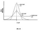
- FIG. 10is a graphical diagram 300 of exemplary optical responses, referred to as D( ⁇ i , ⁇ ), for a diffuser or diffuser material in accordance embodiments of the invention.
- Output from the diffusermay depend on both angle of incidence ⁇ i and on angle of transmission or angle of view, ⁇ .
- the optical transfer function D( ⁇ i , ⁇ )may be expressed as a function of the angle of view “ ⁇ ” and the angle of incidence of light “ ⁇ i ” ranging, e.g., from 0 to 90° or from 0 to ⁇ 90°.
- the vertical axisdepicts the relative intensity of light from a light source that is observed through a diffuser.
- the horizontal axisrepresents the angle of viewing of light communicated through the diffuser.
- the possible angle of viewvaries from 0 to 90 degrees on the right side of graph and from 0 to ⁇ 90 degrees—left side of graph 300 ).
- Curves or traces 310 , 320 , and 330 in FIG. 10depict the optical response of diffusers for a given angle of incidence, ⁇ i as the output varies with transmission angle or view angle ⁇ .
- This angle of incidencemay, for example, be 0° for the plots 310 , 320 , 330 in FIG. 10 .
- the first trace 310depicts the perceived intensity of light versus angle of viewing for a particular diffuser (and a particular angle of incidence).
- the trace 310has a generally a bell-shaped curve that has a relatively sharp peak at a center angle.
- the sharp or relatively narrow peakis located at 0° for this embodiment of the diffuser.
- This narrow peakmay for example have a width as measured at full width half maximum of about 10-30°.
- This type of traceis sometimes referred to as a high gain curve.
- the trace 320depicts an optical response for a second type of diffuser.
- the trace 320is a generally bell-shaped curve that has a relatively small wider peak at its center. This narrow peak may for example have a width as measured at full width half maximum of about 60-100°
- the trace 320with its relatively low peak and thus somewhat flattened response profile is sometimes referred to as a low gain curve.
- each optical responseis shown as centered at about 0° for the purpose of illustration. As will be discussed further below, the optical response may be centered at other angles for different diffusers.
- FIG. 10shows a trace 330 depicting the optical response of an ideal Lambertian diffuser.
- Lambertian diffusersare characterized by a substantially flat angular response profile.
- the trace 330depicts an approximately straight line response having a generally fixed intensity at all angles of viewing.
- non-lambertian diffusersdo not have substantially flat angular response profiles.
- the high gain and low gain diffusers corresponding to traces 310 and 320are examples of non-lambertian diffusers.
- the traces 310 and 320illustrate optical responses of various diffusers having responses that are centered around zero degrees (0°).
- similar shaped (or other shaped) response profilesmay be centered on view angles other than zero degrees, such as, for example, at ten (10), twenty (20), thirty (30), forty (40), 45 (forty five), 50 (fifty), 60 (sixty), 70 (seventy), 80 (eighty) degrees, or on any other view angle.
- D( ⁇ i , ⁇ )may be characterized by a response profile that may be different characteristically for different angles of view.
- the diffuser 201may be a high gain, low gain (or very low gain), or any other suitable type of diffuser therebetween, or any combination thereof.
- the centering of D( ⁇ i , ⁇ ) around a particular angleis relevant to computing a convolution of D( ⁇ i , ⁇ ) and optical response of the interferometric modulator, without the diffuser, which is referred to as R ( ⁇ i , ⁇ )
- FIG. 11is a cross-sectional view illustrating an embodiment of an interferometric modulator display 400 that includes a diffuser 402 .
- the display 400includes an array of interferometric modulators 401 .
- the diffuser 402is physically coupled to a substrate 403 . Light is reflected in the interferometric modulator 401 so as to pass outward through the diffuser 402 .
- the diffuser 402is selected based on its characteristics which influence the reflected light so as to compensate for at least a portion of the angular color shift of the interferometric modulator 401 . This compensation reduces the perceived color shift as the viewing angle of a user of the modulator 401 changes.
- any numerical values used herein, such as the angles of incidence of light paths 410 , 412 , and 414 ,are presented for purposes of illustration and are not necessarily indicative of any embodiment.
- the modulator 401reflects the light further along the paths 410 , 412 , and 414 .
- the light along the paths 410 , 412 , and 414is then incident on the diffuser 402 .
- the diffuser 402redirects portions of the reflected light along a range of optical paths at intensities that depend upon the gain characteristics, D( ⁇ i , ⁇ ), of the diffuser 402 .
- the diffused portion of the light from optical paths 410 , 412 , and 414travels to a viewing position along optical paths 416 .
- These paths 416are at substantially the same angle with respect to the diffuser 402 and substantially parallel for this particular exemplary viewing position 430 which is a distant viewing position.
- the diffuser 402thus operates to collect light that is incident on the modulator 401 at a range of angles and corresponding optical paths, including the paths 410 , 412 , and 414 . This collected light is redirected. A portion of this light is redirected to the viewing position along the optical paths 416 .
- the diffuser 402thus collects light from the modulator 401 (or array of modulators 401 ) at a range of wavelengths to produce a net optical response for the modulator 401 as modified by the diffuser 402 .
- the net optical responseis related to the convolution of the optical response D( ⁇ i , ⁇ ) of the diffuser with the optical response R( ⁇ i , ⁇ ) of the modulator 401 over a range of angles of light incident on the display 400 .
- the net optical response of the system 400can thus be controlled to achieve a desired net optical response.
- the characteristics of the diffuser 402 and the interferometric modulator 401are selected so as to substantially compensate for angular color shift of the interferometric modulator 401 .
- the characteristics of the diffuser 402 and the modulator 401are selected so that an image formed by the modulator array alone is obscured or encrypted and is not visible. The image formed by the modulator array, however, is visible by viewing through the diffuser 402 .
- the overall optical characteristics of the modulator 401 together with the diffuser 402may be modeled in terms of the convolution of the optical response (i.e., spectral reflectance or transfer function) of the modulator 401 , with the optical response of the diffuser 402 .
- An exemplary expression for this convolutionis set forth below.
- the optical response R ( ⁇ i , ⁇ ) of the modulator 401is represented as a function of the angle of incidence, ⁇ i , and wavelength of light, ⁇ , entering the modulator 401 .
- the angle of incidenceis equal to the angle of reflection for specular reflection
- the view angle, ⁇ , for the modulatoris equal to the angle of incidence, ⁇ i , on the modulator.
- R ( ⁇ i , ⁇ )characterizes the optical response of the modulator as a function of view angle, ⁇ .
- the intensity of the light coming out of the diffuser 402is also generally a function of the viewing angle ⁇ (and angle of incidence ⁇ i ). Accordingly, as described above, the optical response of the diffuser is characterized by D( ⁇ i , ⁇ ).
- the view angle, ⁇ , of the modulatorcorresponds to the angle of incidence, ⁇ i , of the diffuser.
- the total or net optical response of the modulator 401 as modified by the diffuser 402may be expressed as R′( ⁇ , ⁇ ) in accordance with the following relation:
- R ′ ⁇ ( ⁇ , ⁇ )⁇ ⁇ i ⁇ D ⁇ ( ⁇ i , ⁇ ) ⁇ R ⁇ ( ⁇ i , ⁇ )
- the modified spectral reflectance R′( ⁇ , ⁇ ) that includes the effects of the diffuser 402can be computed.
- the resultis spectral response of the display for a given view angle ⁇ .
- the spectral response of the combination of the modulator 401 and the diffuser 402can thus be computed for a particular viewing angle and corresponding viewer position.
- the spectral response for the aggregate structure comprising the modulator 401 and the diffuser 402may be computed for multiple viewing angles and view positions to quantify color shift resulting from change in angle of view.
- the type of overall or corrected reflectancei.e., R′( ⁇ , ⁇ )
- R′( ⁇ , ⁇ )in terms of particular criteria, e.g., acceptable or unacceptable level of color shift.
- particular criteriae.g., acceptable or unacceptable level of color shift.
- the color shift at a particular angle of viewe.g., 30 degrees
- the uncompensated optical response R ( ⁇ i , ⁇ ) of the modulator 401 having an undesirable 100-nanometer color shifte.g., at 30 degrees
- R′( ⁇ , ⁇ )the level of tolerance in color shift characteristics may depend on intended use or planned viewing conditions.
- the desirable optical response R′( ⁇ , ⁇ )is derivable from the uncompensated optical response R ( ⁇ i , ⁇ ).
- the optical response of uncompensated R ( ⁇ i , ⁇ ) and desired R′( ⁇ , ⁇ )are known functions
- the optical response (i.e., characteristics) for D( ⁇ i , ⁇ )can be computed from the above equation. Since the above equation has only one unknown variable, D( ⁇ i , ⁇ ) can be determined to define the suitable diffuser for providing the desired spectral responsivity R′( ⁇ , ⁇ ).
- the D( ⁇ i , ⁇ ), once solvedmay, for example, correspond to a diffuser having a high gain, a low gain, or a very low gain response, or other suitable characteristics.
- D( ⁇ i , ⁇ )is determined by solving permutations of the equation above (e.g., solving the deconvolution).
- Well known mathematical and numerical methodsmay be employed to perform the calculations.
- diffusersmay be fabricated to provide a desired optical response. Accordingly, once characteristics of D ( ⁇ i , ⁇ ) are determined, a suitable physical configuration and material of the diffuser 402 may then be determined to produce at least an approximation of the desired response profile D ( ⁇ i , ⁇ ) such that the color shift is within a desired tolerance at the target angle.
- the physical configurationmay be determined using techniques such as are known in the art. Diffusers with selected properties are available, for example, from Nitto Denko, Osaka, Japan. Additional details regarding selecting a diffuser based on the spectral response of the interferometric modulator are discussed more fully below.
- the diffuser 402is a diffuser having high gain characteristics that may be selected to reduce or compensate for the color shift.
- FIG. 12Ais a graphical diagram illustrating the gain of the exemplary diffuser 402 versus angle of view for an angle of incidence of 0°.
- FIG. 12Bis a graphical diagram illustrating the gain of the exemplary diffuser 402 versus angle of view at an angle of incidence of 10°.
- R⁇ i , ⁇
- the calculationsare illustrated using only two angles of incidence for a single wavelength, are provided.
- the convolutionis calculated for angle of incidence ranging from 0 to 10° with a step size of 10°.
- a larger range of anglesmay be used and the step size may be different.
- values for various wavelengthsmay be identified at any particular angle of incidence (or angle of view); in this example, only 0° and 10° are being used.
- wavelengths at each angle of viewthere are many different wavelengths at each angle of view; however only two values (0.5 and 0.9) for the wavelength, ⁇ , are provided at 0 degrees (angle of incidence ⁇ i or angle of view) for illustration only. Similarly, two values (0.6 and 0.8) for the wavelength, ⁇ , are provided at an angle of view of 10 degrees.
- R′( ⁇ , ⁇ )may be compute using the actual optical response D( ⁇ i , ⁇ ) of the diffuser 402 .
- the equation aboveis used to compute R′( ⁇ , ⁇ ) at a desired angle of view.
- R′( ⁇ , ⁇ )can be computed at an angle of view of 10° (or at any desired angle of view, e.g., between 0° and 90°, in a like manner).
- the convolutionis summed by varying ⁇ i ; from 0° to 90° to compute the total modified or compensated optical response R′( ⁇ , ⁇ ) (as corrected by the diffuser 402 ).
- the computationmay operate as follows:
- the diffuser 402may include more than one diffuser layer. In one such embodiment, the same diffuser characteristics may be selected for each of the diffuser layers. In another embodiment, different characteristics may be selected for each of the layers of the diffuser 402 . In one embodiment, the diffuser characteristics of the diffuser 402 may be calculated by convolving the optical responses of each of the layers.
- FIG. 13illustrates a graphical diagram 500 of several spectral reflectance traces for various configurations of interferometric modulator display devices.
- the vertical axisrepresents a reflectance to the viewer, expressed as a percentage (from 0 to 90%).
- the horizontal axisrepresents the wavelength of light that is reflected by the interferometric modulator. This reflectance corresponds to the spectral responsivity e.g., R( ⁇ i , ⁇ ), R′( ⁇ , ⁇ ), described above.
- curve 510depicts a somewhat bell-shaped curve that represents the reflectance as viewed at 0 degrees to normal from the display of one or more interferometric modulators (without the presence of a diffuser layer).
- the peak of curve 510is at approximately 80% reflectance and is centered about 820 nm, which is in the infrared portion of the spectrum.
- FIG. 13further depicts a curve 520 that represents the reflectance of this same display as viewed at 50 degrees to normal.
- the curve 520is shaped similarly to the curve 510 but has a peak value of reflectance of approximately 84% that is located at about 690 nm.
- FIG. 13also depicts a somewhat bell-shaped curve 530 that represents the reflectance as viewed at 0 degrees to normal from a display that includes a diffuser layer.
- the curve 530has a peak gain of approximately 64% that is located approximately at 750 nm.
- FIG. 13depicts a curve 540 that represents the reflectance of the display having the diffuser layer as viewed at 50 degrees to normal.
- the curve 540follows a path that is substantially the same as the path of curve 530 with a slightly smaller peak reflectance value of 62%.
- FIG. 13shows the reflectance from the modulator using input light to the interferometric modulator that is in the infrared portion of the electromagnetic spectrum at about a peak wavelength of 810 nanometers (nm).
- the 50 degree shift in viewing anglecauses an approximately 120 nm color shift in the viewed response profile.
- the curves 530 and 540illustrate the spectral reflectance of the modulator when viewed through a very low gain diffuser 302 having a full width half maximum gain between 120° and 180°.
- the curves 530 and 540represent the convolution of the response of this very low gain diffuser with that of the interferometric modulator. As shown in FIG.
- both curves 530 and 540peak at about the same or a similar wavelength that is horizontally between the peaks of curves 510 and 520 .
- the curvesthus exhibit a very minor perceived color shift (such as in the range of about 10 to 20 nm) when the viewing angle changes by fifty degrees (50°), as in this example.
- the diffuser layerAs compared to the 120 nm color shift of the modulator viewed at 50° without the diffuser layer, the diffuser layer has thus been substantially compensated for the shift in viewing angle.
- the peaks of the curves 530 and 540do not shift in color substantially with changing viewing angle.
- the peaks of curves for the modulator without the diffuser that were in the infrared portion of the spectrumare in the red portion of the spectrum with the low gain diffuser.
- the diffuserhas therefore shifted the spectral responsivity of an interferometric modulator have a peak response in the infrared to a device having a peak in a visible wavelength.
- Another characteristic of the effect of the diffuseris that the peak spectral reflectance of the convoluted, e.g., perceived, light signal is reduced and spread more evenly across the spectrum.
- the color shift and the amount of the drop in peak reflectancemay be controlled by selecting the desired wavelength and angle for the peak of the curve for a diffuser.
- the selected diffusermay have a response that is centered about 0°.
- the selected diffusermay have a response centered around an angle other than 0°, for example, centered at ten (10°), twenty (20), thirty (30), forty (40), 45 (forty five), 50 (fifty), 60 (sixty), 70 (seventy), 80 (eighty) degrees, or on any other view angle.
- FIG. 14is a CIE 1976 chromaticity diagram 600 that illustrates a sequence of data points that show color shift versus view angle to further illustrate the effect of the embodiment of the diffuser 401 from FIG. 13 .
- the horizontal and vertical axesdefine a chromaticity coordinate system on which spectral tri-stimulus values may be depicted.
- a sequence of data points for an interferometric modulator display without diffuseris shown on the gamut color space of the diagram along a trace 605 .
- the curve of the trace 605indicates that there is a considerable color shift for changes in the view angle.
- a single data point 610is shown on the diagram 401 because the color shift has been substantially eliminated by use of the diffuser layer
- a diffusercan be selected having specific properties that produce a desired spectral responsivity, R′( ⁇ , ⁇ ). Examples of properties that can be varied include the shape of the optical response D( ⁇ i , ⁇ ).
- the diffusermay comprise, e.g., a non-lambertian diffuser such as a high gain, low gain, or very low gain diffuser.
- the optical response D( ⁇ i , ⁇ )comprises a peak
- the width of this peakcan be selected. For example, peaks as measured at full width half maximum may be between about 2° to 20° wide in some embodiments or between about 20° to 120° wide or larger or smaller. Peaks widths outside these ranges are also possible.
- the position of this peakcan be controlled.
- the high and low gain response shown in FIG. 10are centered about 0°, in certain embodiments, diffusers having peaked optical response with peak at locations other than 0° may be used. Other properties of the diffuser may be varied as well.
- the optical responses depicted in FIG. 10are for a particular angle of incidence; however, D( ⁇ i , ⁇ ) is also a function of ⁇ i .
- the diffusermay be configured to provide different optical responses D( ⁇ ) for light incident at different angles of incidence ⁇ i .
- the diffusermay be designed such that the width and location of peaks in the optical response are different for differing angles of incidence.
- the peakmay for example be located at an angle of view equal (but opposite) to the angle of incidence.
- the angle of view of the peakmay be different in magnitude from the angle of incidence.
- the spectral responsivity of the interferometric modulatorvaries with angle, different responses for different angles of incidence may be employed to redistribute the rays to achieve the desired dependency of color on view angle. Accordingly, reduced color shift may be achieved by properly distributing the light incident on the diffuser at different angles.
- the desired spectral responsivity R′( ⁇ , ⁇ )may be obtained.
- Consideration of the spectral responsivity R( ⁇ i , ⁇ ) of the interferometric modulatormay be used in determining the properties of such a suitable diffuser. Accordingly, a diffuser may be selected that appropriately matches the interferometric modulator so as, for example, to reduce color shift.
- the selection and/or design of the diffusermay be based on the known spectral and angular optical response of diffuser materials and architectures.
- the diffuseris selected or designed so that the convolution of the diffuser's optical response with that of the interferometric modulator 401 produces an optical response that decreases the color shift.
- the color shift as viewed from at least one target anglemay be reduced to within a predetermined tolerance for a particular viewing angle and particular interferometric modulator configuration 401 .
- the predetermined tolerancemay be expressed as a number of nanometers of color shift.
- Holographic or diffractive optical elementsmay be employed as the diffuser.
- the diffusersmay also be computer generated.
- the desired optical response for the diffuseris produced by selecting materials, thicknesses, and arrangement of the materials of the diffuser to produce the desired optical response for the diffuser.
- the interferometric modulatorhas a spectral response (e.g., for viewing angles at normal incidence) that is centered in the infrared or other non-visible wavelength.
- a spectral responsehaving mostly non-visible components may contribute to reduced color shifting. For example 50%, 60%, 70% or more of the wavelengths under a central peak that extends in the visible may be non-visible. The diffuser may shift this peak into the visible.
- the diffusermay exhibit a response D( ⁇ i , ⁇ , ⁇ ) that is a function of wavelength.
- the diffuserincludes a holographic optical element. Other types of wavelength sensitive diffusers may be employed as well.
- a back light or front lightmay be added to provide additional intensity at desired wavelengths.
- the use of such frequency dependent diffuser configurations and light sourcesprovides additional flexibility in selecting a configuration that may be viewed at a selected angle with a predetermined tolerance on color shift.
- the display 400may include interferometric modulators 401 that have varying optical responses.
- the display 400includes three groups of interferometric modulators 401 having optical responses that, when the modulators 401 are matched with the diffuser 402 as disclosed herein, correspond to red, green, and blue to produce a color display.
- the optical response of diffuser 402may depend on the wavelength ⁇ of light passing through the diffuser 402 .
- the diffuser 402comprises a holographic optical element.
- a combination of several diffusersmay be used to provide a display with angular color shift at a selected angle that is within a predetermined tolerance.
- one or more diffusersmay be used to provide a color shift that is within a predetermined tolerance for two, three, or a range of angles. Still other configurations are possible.
- an application of the interferometric modulator with diffuseris to enable encryption or obscuring of the image of a display to secure the image from unauthorized viewing.
- the diffusermoves data from an invisible portion of the spectrum, e.g., infrared, to a visible portion of the spectrum.
- the diffusermay be positioned with respect to the interferometric modulator array so that authorized viewers receive light from the display through the diffuser.
- the interferometric modulatorproduces an encrypted image and the diffuser is configured to decrypt the image.
- the interferometric modulator array of the displayhas an optical response that is selected to receive input image data and produce an output image that is difficult for the human eye to perceive, for example, in which colors are shifted such that the image is obscured.
- the diffuseris selected to shift the colors to a produce an image with colors indicative of the input image data.
Landscapes
- Physics & Mathematics (AREA)
- General Physics & Mathematics (AREA)
- Optics & Photonics (AREA)
- Spectroscopy & Molecular Physics (AREA)
- Mechanical Light Control Or Optical Switches (AREA)
- Devices For Indicating Variable Information By Combining Individual Elements (AREA)
Abstract
Description
Claims (22)
Priority Applications (14)
| Application Number | Priority Date | Filing Date | Title |
|---|---|---|---|
| US11/040,824US7630123B2 (en) | 2004-09-27 | 2005-01-21 | Method and device for compensating for color shift as a function of angle of view |
| AU2005204303AAU2005204303A1 (en) | 2004-09-27 | 2005-08-30 | Method and device for compensating for color shift as a function of angle of view |
| TW094130570ATW200624368A (en) | 2004-09-27 | 2005-09-06 | Method and device for compensating for color shift as a function of angle of view |
| JP2005261026AJP2006099102A (en) | 2004-09-27 | 2005-09-08 | Method and device of being compensated to collar shifting as function of field angle |
| CA002519485ACA2519485A1 (en) | 2004-09-27 | 2005-09-13 | Method and device for compensating for color shift as a function of angle of view |
| EP05255647AEP1640314A3 (en) | 2004-09-27 | 2005-09-14 | Method and device for compensating for color shift as a function of angle of view |
| EP11157386AEP2388234A1 (en) | 2004-09-27 | 2005-09-14 | Method and device for compensating for color shift as a function of angle of view |
| SG200506022ASG121151A1 (en) | 2004-09-27 | 2005-09-19 | Method and device for compensating for color shiftas a function of angle of view |
| MXPA05010094AMXPA05010094A (en) | 2004-09-27 | 2005-09-21 | Method and device for compensating for color shift as a function of angle of view. |
| RU2005129902/28ARU2005129902A (en) | 2004-09-27 | 2005-09-26 | METHOD AND DEVICE FOR COMPENSATION OF COLOR SHIFT AS VISION ANGLE FUNCTIONS |
| BRPI0503907-0ABRPI0503907A (en) | 2004-09-27 | 2005-09-27 | method and device for compensating for change in color as a function of the viewing angle |
| KR1020050090052AKR101236289B1 (en) | 2004-09-27 | 2005-09-27 | Method and device for compensating for color shift as a function of angle of view |
| US12/631,686US8045256B2 (en) | 2004-09-27 | 2009-12-04 | Method and device for compensating for color shift as a function of angle of view |
| US13/229,467US8861071B2 (en) | 2004-09-27 | 2011-09-09 | Method and device for compensating for color shift as a function of angle of view |
Applications Claiming Priority (2)
| Application Number | Priority Date | Filing Date | Title |
|---|---|---|---|
| US61397804P | 2004-09-27 | 2004-09-27 | |
| US11/040,824US7630123B2 (en) | 2004-09-27 | 2005-01-21 | Method and device for compensating for color shift as a function of angle of view |
Related Child Applications (1)
| Application Number | Title | Priority Date | Filing Date |
|---|---|---|---|
| US12/631,686DivisionUS8045256B2 (en) | 2004-09-27 | 2009-12-04 | Method and device for compensating for color shift as a function of angle of view |
Publications (2)
| Publication Number | Publication Date |
|---|---|
| US20060077522A1 US20060077522A1 (en) | 2006-04-13 |
| US7630123B2true US7630123B2 (en) | 2009-12-08 |
Family
ID=35462167
Family Applications (3)
| Application Number | Title | Priority Date | Filing Date |
|---|---|---|---|
| US11/040,824Expired - Fee RelatedUS7630123B2 (en) | 2004-09-27 | 2005-01-21 | Method and device for compensating for color shift as a function of angle of view |
| US12/631,686Expired - Fee RelatedUS8045256B2 (en) | 2004-09-27 | 2009-12-04 | Method and device for compensating for color shift as a function of angle of view |
| US13/229,467Active2026-02-21US8861071B2 (en) | 2004-09-27 | 2011-09-09 | Method and device for compensating for color shift as a function of angle of view |
Family Applications After (2)
| Application Number | Title | Priority Date | Filing Date |
|---|---|---|---|
| US12/631,686Expired - Fee RelatedUS8045256B2 (en) | 2004-09-27 | 2009-12-04 | Method and device for compensating for color shift as a function of angle of view |
| US13/229,467Active2026-02-21US8861071B2 (en) | 2004-09-27 | 2011-09-09 | Method and device for compensating for color shift as a function of angle of view |
Country Status (11)
| Country | Link |
|---|---|
| US (3) | US7630123B2 (en) |
| EP (2) | EP1640314A3 (en) |
| JP (1) | JP2006099102A (en) |
| KR (1) | KR101236289B1 (en) |
| AU (1) | AU2005204303A1 (en) |
| BR (1) | BRPI0503907A (en) |
| CA (1) | CA2519485A1 (en) |
| MX (1) | MXPA05010094A (en) |
| RU (1) | RU2005129902A (en) |
| SG (1) | SG121151A1 (en) |
| TW (1) | TW200624368A (en) |
Cited By (30)
| Publication number | Priority date | Publication date | Assignee | Title |
|---|---|---|---|---|
| US7813026B2 (en) | 2004-09-27 | 2010-10-12 | Qualcomm Mems Technologies, Inc. | System and method of reducing color shift in a display |
| US7845841B2 (en) | 2006-08-28 | 2010-12-07 | Qualcomm Mems Technologies, Inc. | Angle sweeping holographic illuminator |
| US7864395B2 (en) | 2006-10-27 | 2011-01-04 | Qualcomm Mems Technologies, Inc. | Light guide including optical scattering elements and a method of manufacture |
| US7907319B2 (en) | 1995-11-06 | 2011-03-15 | Qualcomm Mems Technologies, Inc. | Method and device for modulating light with optical compensation |
| US7933475B2 (en) | 2006-02-17 | 2011-04-26 | Qualcomm Mems Technologies, Inc. | Method and apparatus for providing back-lighting in a display device |
| US20110199669A1 (en)* | 2004-09-27 | 2011-08-18 | Qualcomm Mems Technologies, Inc. | Systems and methods using interferometric optical modulators and diffusers |
| US8004504B2 (en) | 2004-09-27 | 2011-08-23 | Qualcomm Mems Technologies, Inc. | Reduced capacitance display element |
| US8040589B2 (en) | 2008-02-12 | 2011-10-18 | Qualcomm Mems Technologies, Inc. | Devices and methods for enhancing brightness of displays using angle conversion layers |
| US8045252B2 (en) | 2004-02-03 | 2011-10-25 | Qualcomm Mems Technologies, Inc. | Spatial light modulator with integrated optical compensation structure |
| US8045256B2 (en) | 2004-09-27 | 2011-10-25 | Qualcomm Mems Technologies, Inc. | Method and device for compensating for color shift as a function of angle of view |
| US8049951B2 (en) | 2008-04-15 | 2011-11-01 | Qualcomm Mems Technologies, Inc. | Light with bi-directional propagation |
| US8061882B2 (en) | 2006-10-06 | 2011-11-22 | Qualcomm Mems Technologies, Inc. | Illumination device with built-in light coupler |
| US8068710B2 (en) | 2007-12-07 | 2011-11-29 | Qualcomm Mems Technologies, Inc. | Decoupled holographic film and diffuser |
| US8072402B2 (en) | 2007-08-29 | 2011-12-06 | Qualcomm Mems Technologies, Inc. | Interferometric optical modulator with broadband reflection characteristics |
| US8094362B2 (en) | 2004-03-06 | 2012-01-10 | Qualcomm Mems Technologies, Inc. | Method and system for color optimization in a display |
| US8111446B2 (en) | 2004-09-27 | 2012-02-07 | Qualcomm Mems Technologies, Inc. | Optical films for controlling angular characteristics of displays |
| US8284475B2 (en) | 2007-05-11 | 2012-10-09 | Qualcomm Mems Technologies, Inc. | Methods of fabricating MEMS with spacers between plates and devices formed by same |
| US8300304B2 (en) | 2008-02-12 | 2012-10-30 | Qualcomm Mems Technologies, Inc. | Integrated front light diffuser for reflective displays |
| US8368981B2 (en) | 2006-10-10 | 2013-02-05 | Qualcomm Mems Technologies, Inc. | Display device with diffractive optics |
| US8416487B2 (en) | 1999-10-05 | 2013-04-09 | Qualcomm Mems Technologies, Inc. | Photonic MEMS and structures |
| US8670171B2 (en) | 2010-10-18 | 2014-03-11 | Qualcomm Mems Technologies, Inc. | Display having an embedded microlens array |
| US8717660B2 (en)* | 2012-07-03 | 2014-05-06 | Qualcomm Mems Technologies, Inc. | Annulus scattering diffuser for reflective display |
| US8736949B2 (en) | 2007-07-31 | 2014-05-27 | Qualcomm Mems Technologies, Inc. | Devices and methods for enhancing color shift of interferometric modulators |
| US8872085B2 (en) | 2006-10-06 | 2014-10-28 | Qualcomm Mems Technologies, Inc. | Display device having front illuminator with turning features |
| US8902484B2 (en) | 2010-12-15 | 2014-12-02 | Qualcomm Mems Technologies, Inc. | Holographic brightness enhancement film |
| US8928967B2 (en) | 1998-04-08 | 2015-01-06 | Qualcomm Mems Technologies, Inc. | Method and device for modulating light |
| US8971675B2 (en) | 2006-01-13 | 2015-03-03 | Qualcomm Mems Technologies, Inc. | Interconnect structure for MEMS device |
| US9019183B2 (en) | 2006-10-06 | 2015-04-28 | Qualcomm Mems Technologies, Inc. | Optical loss structure integrated in an illumination apparatus |
| US9025235B2 (en) | 2002-12-25 | 2015-05-05 | Qualcomm Mems Technologies, Inc. | Optical interference type of color display having optical diffusion layer between substrate and electrode |
| US9110289B2 (en) | 1998-04-08 | 2015-08-18 | Qualcomm Mems Technologies, Inc. | Device for modulating light with multiple electrodes |
Families Citing this family (8)
| Publication number | Priority date | Publication date | Assignee | Title |
|---|---|---|---|---|
| US7777954B2 (en)* | 2007-01-30 | 2010-08-17 | Qualcomm Mems Technologies, Inc. | Systems and methods of providing a light guiding layer |
| US8111262B2 (en)* | 2007-05-18 | 2012-02-07 | Qualcomm Mems Technologies, Inc. | Interferometric modulator displays with reduced color sensitivity |
| US8986812B2 (en) | 2007-07-09 | 2015-03-24 | 3M Innovative Properties Company | Thin microstructured optical films |
| US7864403B2 (en)* | 2009-03-27 | 2011-01-04 | Qualcomm Mems Technologies, Inc. | Post-release adjustment of interferometric modulator reflectivity |
| CN108281111A (en)* | 2018-01-19 | 2018-07-13 | 云谷(固安)科技有限公司 | Display control method and device |
| US12007593B2 (en) | 2018-04-18 | 2024-06-11 | 3M Innovative Properties Company | Organic light emitting diode with color-correction for maximum white-point color shift |
| US11726365B1 (en) | 2020-07-10 | 2023-08-15 | Meta Platforms Technologies, Llc | Optical assembly for providing koehller illumination to a display |
| US11862083B2 (en) | 2020-08-13 | 2024-01-02 | Apple Inc. | Electronic devices with curved display surfaces |
Citations (221)
| Publication number | Priority date | Publication date | Assignee | Title |
|---|---|---|---|---|
| US3813265A (en) | 1970-02-16 | 1974-05-28 | A Marks | Electro-optical dipolar material |
| DE3402746A1 (en) | 1984-01-27 | 1985-08-08 | Robert Bosch Gmbh, 7000 Stuttgart | Liquid crystal display |
| JPS629317B2 (en) | 1979-05-05 | 1987-02-27 | Krupp Gmbh | |
| EP0278038A1 (en) | 1987-02-13 | 1988-08-17 | Battelle-Institut e.V. | Active flat type display panel |
| US4832459A (en) | 1984-02-06 | 1989-05-23 | Rogers Corporation | Backlighting for electro-optical passive displays and transflective layer useful therewith |
| US4850682A (en) | 1986-07-14 | 1989-07-25 | Advanced Environmental Research Group | Diffraction grating structures |
| US4961617A (en) | 1989-07-19 | 1990-10-09 | Ferrydon Shahidi | Fibre optic waveguide illuminating elements |
| JPH0481816B2 (en) | 1985-08-26 | 1992-12-25 | Matsushita Electric Ind Co Ltd | |
| GB2260203A (en) | 1991-10-04 | 1993-04-07 | Marconi Gec Ltd | Transmissive colour display system illuminated using a holographic element |
| JPH05281479A (en) | 1992-03-31 | 1993-10-29 | Nippon Steel Corp | Display device |
| US5289300A (en) | 1991-02-04 | 1994-02-22 | Semiconductor Energy Laboratory Co., Ltd. | Method of manufacturing electro-optical devices wherein the electrode is patterned on the modulation layer |
| US5293272A (en) | 1992-08-24 | 1994-03-08 | Physical Optics Corporation | High finesse holographic fabry-perot etalon and method of fabricating |
| GB2278222A (en) | 1993-05-20 | 1994-11-23 | Sharp Kk | Spatial light modulator |
| WO1995001584A1 (en) | 1993-07-01 | 1995-01-12 | Alliedsignal Inc. | Direct view display device with array of tapered waveguide |
| US5398125A (en) | 1993-11-10 | 1995-03-14 | Minnesota Mining And Manufacturing Company | Liquid crystal projection panel having microlens arrays, on each side of the liquid crystal, with a focus beyond the liquid crystal |
| WO1995014256A1 (en) | 1993-11-15 | 1995-05-26 | Alliedsignal Inc. | Optical element for use in an array of optical elements in a display arrangement |
| US5452385A (en) | 1993-03-09 | 1995-09-19 | Sharp Kabushiki Kaisha | Optical scanning device an optical scanning type display and an image data input/output device |
| US5459610A (en) | 1992-04-28 | 1995-10-17 | The Board Of Trustees Of The Leland Stanford, Junior University | Deformable grating apparatus for modulating a light beam and including means for obviating stiction between grating elements and underlying substrate |
| US5467417A (en) | 1992-09-16 | 1995-11-14 | Hitachi, Ltd. | Prism plate for efficiently emitting light flux within a predetermined range, and liquid crystal indicator and indicator illumination method using the same |
| US5515184A (en) | 1991-11-12 | 1996-05-07 | The University Of Alabama In Huntsville | Waveguide hologram illuminators |
| US5569565A (en) | 1991-05-23 | 1996-10-29 | Matsushita Electric Industrial Co., Ltd. | Hologram recording material |
| WO1997001240A1 (en) | 1995-06-20 | 1997-01-09 | Thomson Consumer Electronics, Inc. | Back lit electronic viewfinder |
| US5594830A (en) | 1992-03-23 | 1997-01-14 | Minnesota Mining And Manufacturing Co. | Luminaire device |
| JPH0922012A (en) | 1995-07-06 | 1997-01-21 | Mitsubishi Rayon Co Ltd | Backlight and liquid crystal display device using the same |
| WO1997016756A1 (en) | 1995-11-01 | 1997-05-09 | Matsushita Electric Industrial Co., Ltd. | Outgoing efficiency control device, projection type display apparatus, infrared sensor and non-contact thermometer |
| WO1997017628A1 (en) | 1995-11-06 | 1997-05-15 | Etalon, Inc. | Interferometric modulation |
| US5638084A (en) | 1992-05-22 | 1997-06-10 | Dielectric Systems International, Inc. | Lighting-independent color video display |
| US5650865A (en) | 1995-03-21 | 1997-07-22 | Hughes Electronics | Holographic backlight for flat panel displays |
| US5659410A (en) | 1993-12-28 | 1997-08-19 | Enplas Corporation | Surface light source device and liquid crystal display |
| JPH09281917A (en) | 1996-04-17 | 1997-10-31 | Dainippon Printing Co Ltd | Image display device using hologram color filter |
| DE19622748A1 (en) | 1996-06-05 | 1997-12-11 | Forschungszentrum Juelich Gmbh | Interference filter based on porous silicon |
| US5703667A (en) | 1996-05-31 | 1997-12-30 | Shimada Precision, Co., Ltd. | Light guide plates and light guide plate assembly utilizing diffraction grating |
| EP0822441A2 (en) | 1996-08-01 | 1998-02-04 | Sharp Kabushiki Kaisha | Optical device and directional display |
| US5735590A (en) | 1994-03-02 | 1998-04-07 | Tosoh Corporation | Backlighting device with a transparent sheet having straight ridges |
| US5771321A (en) | 1996-01-04 | 1998-06-23 | Massachusetts Institute Of Technology | Micromechanical optical switch and flat panel display |
| US5770626A (en) | 1987-08-19 | 1998-06-23 | Hoffmann-La Roche Inc. | Tetrahydronaphtalene and indane compounds useful for reversing the photodamage in sun-exposed skin |
| US5783614A (en) | 1997-02-21 | 1998-07-21 | Copytele, Inc. | Polymeric-coated dielectric particles and formulation and method for preparing same |
| WO1998032047A1 (en) | 1997-01-16 | 1998-07-23 | Motorola Inc. | Ambient illuminated electro-optic display device |
| JPH10202948A (en) | 1997-01-29 | 1998-08-04 | Canon Inc | Image forming apparatus and image forming method of image forming apparatus |
| US5793504A (en) | 1996-08-07 | 1998-08-11 | Northrop Grumman Corporation | Hybrid angular/spatial holographic multiplexer |
| WO1998035182A1 (en) | 1997-02-07 | 1998-08-13 | Alliedsignal Inc. | Reflective display |
| US5810464A (en) | 1995-02-03 | 1998-09-22 | Enplas Corporation | Surface light source device of side light type |
| US5815229A (en) | 1994-11-21 | 1998-09-29 | Proxima Corporation | Microlens imbedded liquid crystal projection panel including thermal insulation layer |
| US5854872A (en) | 1996-10-08 | 1998-12-29 | Clio Technologies, Inc. | Divergent angle rotator system and method for collimating light beams |
| US5877874A (en) | 1995-08-24 | 1999-03-02 | Terrasun L.L.C. | Device for concentrating optical radiation |
| US5892598A (en) | 1994-07-15 | 1999-04-06 | Matsushita Electric Industrial Co., Ltd. | Head up display unit, liquid crystal display panel, and method of fabricating the liquid crystal display panel |
| EP0879991A3 (en) | 1997-05-13 | 1999-04-21 | Matsushita Electric Industrial Co., Ltd. | Illuminating system |
| US5914804A (en) | 1998-01-28 | 1999-06-22 | Lucent Technologies Inc | Double-cavity micromechanical optical modulator with plural multilayer mirrors |
| JPH11174234A (en) | 1997-12-05 | 1999-07-02 | Victor Co Of Japan Ltd | Hologram color filter, manufacture of hologram color filter and spatial light modulation device using the same |
| US5933183A (en) | 1995-12-12 | 1999-08-03 | Fuji Photo Film Co., Ltd. | Color spatial light modulator and color printer using the same |
| JPH11232919A (en) | 1998-02-17 | 1999-08-27 | Fuji Xerox Co Ltd | Front light lighting system and reflecting type display device |
| US5982540A (en) | 1994-03-16 | 1999-11-09 | Enplas Corporation | Surface light source device with polarization function |
| EP0957392A1 (en) | 1998-05-11 | 1999-11-17 | Nitto Denko Corporation | Reflection type liquid-crystal display unit |
| US5991073A (en) | 1996-01-26 | 1999-11-23 | Sharp Kabushiki Kaisha | Autostereoscopic display including a viewing window that may receive black view data |
| WO1999063394A1 (en) | 1998-06-02 | 1999-12-09 | Nissha Printing Co., Ltd. | Touch screen with front lighting |
| US6014192A (en) | 1996-07-16 | 2000-01-11 | Thomson-Csf | Illumination device and application thereof to the illumination of a transmissive screen |
| US6040937A (en) | 1994-05-05 | 2000-03-21 | Etalon, Inc. | Interferometric modulation |
| US6048071A (en) | 1997-03-28 | 2000-04-11 | Sharp Kabushiki Kaisha | Front illumination device and reflection-type liquid crystal display device incorporating same |
| US6049317A (en) | 1989-02-27 | 2000-04-11 | Texas Instruments Incorporated | System for imaging of light-sensitive media |
| US6073034A (en) | 1996-10-31 | 2000-06-06 | Kopin Corporation | Wireless telephone display system |
| US6091469A (en) | 1998-05-19 | 2000-07-18 | Dai Nippon Printing Co., Ltd. | Light reflector for use in a reflective-type liquid-crystal display |
| JP2000305074A (en) | 1999-04-26 | 2000-11-02 | Dainippon Printing Co Ltd | Reflective liquid crystal display |
| US6195196B1 (en) | 1998-03-13 | 2001-02-27 | Fuji Photo Film Co., Ltd. | Array-type exposing device and flat type display incorporating light modulator and driving method thereof |
| US6196691B1 (en) | 1998-04-01 | 2001-03-06 | Shimada Precision, Co., Ltd. | Light guide plate for point source |
| EP1081633A2 (en) | 1999-08-31 | 2001-03-07 | Daicel Chemical Industries, Ltd. | Touch panel and display device using the same |
| US6211976B1 (en) | 1998-09-14 | 2001-04-03 | Digilens, Inc. | Holographic projection system |
| EP1089115A1 (en) | 1999-10-02 | 2001-04-04 | Sharp Kabushiki Kaisha | Optical device and projection display |
| US6243149B1 (en) | 1994-10-27 | 2001-06-05 | Massachusetts Institute Of Technology | Method of imaging using a liquid crystal display device |
| WO2001057434A1 (en) | 2000-02-04 | 2001-08-09 | Robert Bosch Gmbh | Display device |
| US6282010B1 (en) | 1998-05-14 | 2001-08-28 | Texas Instruments Incorporated | Anti-reflective coatings for spatial light modulators |
| US20010019380A1 (en) | 2000-03-03 | 2001-09-06 | Takayuki Ishihara | Lighting unit and liquid crystal display utilizing the same |
| US20010030861A1 (en) | 1996-02-01 | 2001-10-18 | Mitsubishi Rayon Co., Ltd. | Surface light source device, and liquid crystal display device, sign display apparatus and traffic sign display apparatus using the surface light source device |
| JP2001305312A (en) | 2000-03-31 | 2001-10-31 | Three M Innovative Properties Co | Optical laminated body |
| US20010049061A1 (en) | 1997-12-05 | 2001-12-06 | Shintaro Nakagaki | Method for producing hologram lens, method for producing hologram color filter, and space light modulating apparatuses using the hologram lens and the hologram color filter respectively |
| JP2001343514A (en) | 2000-05-30 | 2001-12-14 | Victor Co Of Japan Ltd | Hologram color filter |
| US20010055208A1 (en) | 2000-06-15 | 2001-12-27 | Koichi Kimura | Optical element, optical light source unit and optical display device equipped with the optical light source unit |
| WO2002006858A2 (en) | 2000-07-18 | 2002-01-24 | Optaglio Limited | Achromatic diffractive device |
| US6356378B1 (en) | 1995-06-19 | 2002-03-12 | Reflectivity, Inc. | Double substrate reflective spatial light modulator |
| US20020034071A1 (en) | 2000-09-20 | 2002-03-21 | Sanyo Electric Co., Ltd. | Beam light source and lighting device using same |
| JP2002090549A (en) | 2000-09-13 | 2002-03-27 | Shimada Precision Kk | Front light light guide plate |
| EP1199512A1 (en) | 2000-10-11 | 2002-04-24 | Nitto Denko Corporation | Glass substrate and liquid-crystal display device |
| US6381022B1 (en) | 1992-01-22 | 2002-04-30 | Northeastern University | Light modulating device |
| US20020054258A1 (en) | 2000-11-08 | 2002-05-09 | Nitto Denko Corporation | Optical film and reflective liquid-crystal display device |
| JP2002174780A (en) | 2000-12-08 | 2002-06-21 | Stanley Electric Co Ltd | Reflective color display |
| US20020080465A1 (en) | 2000-11-03 | 2002-06-27 | Intpax, Inc. | MEMS based variable optical attenuator (MBVOA) |
| US6412969B1 (en) | 1998-12-14 | 2002-07-02 | Sharp Kabushiki Kaisha | Backlighting device and a method of manufacturing the same, and a liquid crystal display apparatus |
| EP1222586A2 (en) | 1999-08-31 | 2002-07-17 | Accenture LLP | A system, method and article of manufacture for organizing multiple dimensions of tax data for the purpose of generating tax-related fact details |
| US20020105699A1 (en) | 2001-02-02 | 2002-08-08 | Teravicta Technologies, Inc | Integrated optical micro-electromechanical systems and methods of fabricating and operating the same |
| US20020126364A1 (en) | 1994-05-05 | 2002-09-12 | Iridigm Display Corporation, A Delaware Corporation | Interferometric modulation of radiation |
| WO2002071132A2 (en) | 2001-03-02 | 2002-09-12 | Massachusetts Institute Of Technology | Methods and apparatus for diffractive optical processing using an actuatable structure |
| US20020135560A1 (en) | 2001-03-26 | 2002-09-26 | Minebea Co., Ltd. | Spread illuminating apparatus with multi-layer light conductive member |
| US20020149584A1 (en) | 2001-04-13 | 2002-10-17 | Simpson John T. | Reflective coherent spatial light modulator |
| US20020154256A1 (en) | 2001-02-09 | 2002-10-24 | Fujitsu Limited | Liquid-crystal display and a lighting apparatus |
| US20020172039A1 (en) | 2001-05-16 | 2002-11-21 | Ben-Zion Inditsky | Ultra-thin backlight |
| US20020180915A1 (en) | 2001-06-01 | 2002-12-05 | Dai Nippon Printing Co., Ltd. | Wavelength-selecting optical element and optical display provided with the same |
| US20020180910A1 (en) | 2001-05-07 | 2002-12-05 | Nitto Denko Corporation | Reflective liquid-crystal display device |
| US6493475B1 (en) | 2000-10-19 | 2002-12-10 | Tellium, Inc. | Monolithic integration of signal-monitoring scheme in an optical switch |
| EP1279892A1 (en) | 2001-07-27 | 2003-01-29 | Nissen Chemitec Corporation | Planar lighting device |
| US6522794B1 (en) | 1994-09-09 | 2003-02-18 | Gemfire Corporation | Display panel with electrically-controlled waveguide-routing |
| JP2003057652A (en) | 2001-08-20 | 2003-02-26 | Japan Science & Technology Corp | Image display devices, lighting devices |
| JP2003066451A (en) | 2001-08-30 | 2003-03-05 | Matsushita Electric Ind Co Ltd | Liquid crystal display |
| US6538813B1 (en) | 2000-09-19 | 2003-03-25 | Honeywell International Inc. | Display screen with metallized tapered waveguides |
| US20030067760A1 (en) | 2001-09-26 | 2003-04-10 | Jagt Hendrik Johannes Boudewijn | Waveguide, edge-lit illumination arrangement and display comprising such |
| WO2003032058A1 (en) | 2001-10-11 | 2003-04-17 | Deep Video Imaging Limited | Visual display unit illumination |
| US20030083429A1 (en) | 1995-09-28 | 2003-05-01 | Alliedsignal Inc. | Colored articles and compositions and methods for their fabrication |
| US6574033B1 (en) | 2002-02-27 | 2003-06-03 | Iridigm Display Corporation | Microelectromechanical systems device and method for fabricating same |
| US20030103177A1 (en) | 2001-04-10 | 2003-06-05 | Seiko Epson Corporation | Liquid crystal device and electronic apparatus |
| JP2003177336A (en) | 2001-12-11 | 2003-06-27 | Fuji Photo Film Co Ltd | Optical modulating element, optical modulating element array, and exposure device using the same |
| WO2003056876A2 (en) | 2001-12-14 | 2003-07-10 | Digital Optics International Corporation | Uniform illumination system |
| US6598987B1 (en) | 2000-06-15 | 2003-07-29 | Nokia Mobile Phones Limited | Method and apparatus for distributing light to the user interface of an electronic device |
| WO2003062912A1 (en) | 2002-01-25 | 2003-07-31 | Koninklijke Philips Electronics N.V. | Display device |
| US20030151821A1 (en) | 2001-12-19 | 2003-08-14 | Favalora Gregg E. | Radiation conditioning system |
| US20030160919A1 (en) | 2002-02-28 | 2003-08-28 | Mitsubishi Denki Kabushiki Kaisha | Liquid crystal display device |
| US20030161040A1 (en) | 2002-02-26 | 2003-08-28 | Namco Ltd. | Stereoscopic image display device and electronic apparatus |
| EP1347315A1 (en) | 2000-12-28 | 2003-09-24 | Fuji Electric Co., Ltd. | Light guiding plate and liquid crystal display device with the light guiding plate |
| US20030184690A1 (en) | 2000-04-21 | 2003-10-02 | Akifumi Ogiwara | Illuminator, image display comprising the same, liquid crystal television, liquid crystal monitor, and liquid crystal information terminal |
| US6636322B1 (en) | 1999-05-07 | 2003-10-21 | Sharp Kabushiki Kaisha | Method and device for measuring cell gap of liquid crystal display using near-IR radiation |
| US6642913B1 (en) | 1999-01-20 | 2003-11-04 | Fuji Photo Film Co., Ltd. | Light modulation element, exposure unit, and flat-panel display unit |
| JP2003315694A (en) | 2002-04-25 | 2003-11-06 | Fuji Photo Film Co Ltd | Image display element and image display device using the same |
| US6646772B1 (en) | 1999-09-14 | 2003-11-11 | Digilens, Inc. | Holographic illumination system |
| US20030210363A1 (en) | 2000-04-21 | 2003-11-13 | Seiko Epson Corporation | Electrooptical device, projection-type display apparatus, and method for manufacturing the electrooptical device |
| US6650455B2 (en) | 1994-05-05 | 2003-11-18 | Iridigm Display Corporation | Photonic mems and structures |
| US6653616B2 (en) | 2002-01-11 | 2003-11-25 | Alcor Micro, Corp. | Device for processing output signals from a photo-diode |
| US6669350B2 (en) | 2000-12-14 | 2003-12-30 | Mitsubish Rayon Co., Ltd. | Planar light source system and light deflecting device therefor |
| US6674562B1 (en) | 1994-05-05 | 2004-01-06 | Iridigm Display Corporation | Interferometric modulation of radiation |
| WO2004006003A1 (en) | 2002-07-02 | 2004-01-15 | Iridigm Display Corporation | A device having a light-absorbing mask a method for fabricating same |
| US20040032401A1 (en) | 2002-08-19 | 2004-02-19 | Fujitsu Limited | Touch panel device |
| EP1329664A4 (en) | 2000-09-25 | 2004-03-03 | Mitsubishi Rayon Co | LIGHTING DEVICE |
| US20040051929A1 (en) | 1994-05-05 | 2004-03-18 | Sampsell Jeffrey Brian | Separable modulator |
| WO2004027514A2 (en) | 2002-09-20 | 2004-04-01 | Honeywell International, Inc. | High efficiency viewing screen |
| EP1413543A1 (en) | 2002-10-24 | 2004-04-28 | Hewlett-Packard Development Company, L.P. | Micro electro mechanical (MEMS) actuated colour light modulator grating and method for its manufacture |
| WO2004036270A1 (en) | 2002-10-14 | 2004-04-29 | 3M Innovative Properties Company | Antireflection films for use with displays |
| WO2003038509B1 (en) | 2001-11-01 | 2004-05-06 | Motorola Inc | Reflective liquid crystal display with improved contrast |
| US6738194B1 (en) | 2002-07-22 | 2004-05-18 | The United States Of America As Represented By The Secretary Of The Navy | Resonance tunable optical filter |
| US6742921B2 (en) | 2000-06-26 | 2004-06-01 | Nitto Denko Corporation | Light pipe, plate light source unit and reflection type liquid-crystal display device |
| WO2003075207A3 (en) | 2002-03-01 | 2004-06-10 | Planar Systems Inc | Reflection resistant touch screens |
| US20040125281A1 (en) | 2002-12-25 | 2004-07-01 | Wen-Jian Lin | Optical interference type of color display |
| US20040125048A1 (en) | 2002-09-20 | 2004-07-01 | Toshihiro Fukuda | Display element , display device, and microlens array |
| US6760135B1 (en) | 1999-06-09 | 2004-07-06 | Holographic Imaging Llc | Holographic displays |
| US6774962B2 (en) | 2001-11-08 | 2004-08-10 | Lg.Philips Lcd Co., Ltd. | Liquid crystal display device using cholesteric liquid crystal and a manufacturing method thereof |
| US6773126B1 (en) | 1999-05-28 | 2004-08-10 | Oy Modilis Ltd. | Light panel with improved diffraction |
| DE10228946B4 (en) | 2002-06-28 | 2004-08-26 | Universität Bremen | Optical modulator, display, use of an optical modulator and method for producing an optical modulator |
| US6794119B2 (en) | 2002-02-12 | 2004-09-21 | Iridigm Display Corporation | Method for fabricating a structure for a microelectromechanical systems (MEMS) device |
| US20040207995A1 (en) | 2003-04-18 | 2004-10-21 | Park Jong Hwa | Light unit for display device |
| US6819469B1 (en) | 2003-05-05 | 2004-11-16 | Igor M. Koba | High-resolution spatial light modulator for 3-dimensional holographic display |
| US6822745B2 (en)* | 2000-01-25 | 2004-11-23 | Zygo Corporation | Optical systems for measuring form and geometric dimensions of precision engineered parts |
| US20040233357A1 (en) | 2001-10-02 | 2004-11-25 | Sharp Kabushiki Kaisha | Liquid crystal display device |
| US20040246743A1 (en) | 2001-06-30 | 2004-12-09 | Lee Moon-Gyu | Backlight using planar hologram for flat display device |
| US6841787B2 (en) | 2001-11-07 | 2005-01-11 | Applied Materials, Inc. | Maskless photon-electron spot-grid array printer |
| US20050010568A1 (en) | 2002-11-29 | 2005-01-13 | Casio Computer Co., Ltd. | Portable wireless communication terminal, picked-up image editing apparatus, and picked-up image editing method |
| WO2005011012A1 (en) | 2003-07-21 | 2005-02-03 | Schott Ag | Luminous element |
| US20050069254A1 (en) | 2003-08-08 | 2005-03-31 | Bernd Schultheis | Method for producing light-scattering structures on flat optical waveguides |
| US6879354B1 (en) | 1997-03-28 | 2005-04-12 | Sharp Kabushiki Kaisha | Front-illuminating device and a reflection-type liquid crystal display using such a device |
| US6885377B2 (en) | 2001-11-19 | 2005-04-26 | Samsung Electronics Co., Ltd. | Image data output controller using double buffering |
| US20050120553A1 (en) | 2003-12-08 | 2005-06-09 | Brown Dirk D. | Method for forming MEMS grid array connector |
| US20050133761A1 (en) | 2003-12-19 | 2005-06-23 | Robbie Thielemans | Broadband full white reflective display structure |
| US20050141065A1 (en) | 2003-12-22 | 2005-06-30 | Taketoshi Masamoto | Illuminating device, electro-optical device, and electronic apparatus |
| US20050146897A1 (en) | 2002-03-14 | 2005-07-07 | Nec Corporation | Optical modulating/display device and production method therefor and display apparatus mounting the optical modulating/displaying device thereon |
| US6917469B2 (en) | 2003-06-27 | 2005-07-12 | Japan Acryace Co., Ltd. | Light diffusing laminated plate |
| US20050179977A1 (en)* | 2004-02-03 | 2005-08-18 | Clarence Chui | Spatial light modulator with integrated optical compensation structure |
| US20050195468A1 (en)* | 2004-03-05 | 2005-09-08 | Sampsell Jeffrey B. | Integrated modulator illumination |
| EP1577701A1 (en) | 2004-03-17 | 2005-09-21 | National Institute of Advanced Industrial Science and Technology | Reflective light control element with diffusely reflecting surface |
| WO2005088367A1 (en) | 2004-02-13 | 2005-09-22 | Nokia Corporation | Method of manufacturing a light guide |
| US20050231977A1 (en) | 2002-07-01 | 2005-10-20 | Matsushita Electric Industrial Co., Ltd. | Portable terminal apparatus |
| US6967779B2 (en) | 1998-04-15 | 2005-11-22 | Bright View Technologies, Inc. | Micro-lens array with precisely aligned aperture mask and methods of producing same |
| US20050259939A1 (en) | 2004-04-30 | 2005-11-24 | Kari Rinko | Ultra thin lighting element |
| US6970031B1 (en) | 2004-05-28 | 2005-11-29 | Hewlett-Packard Development Company, L.P. | Method and apparatus for reducing charge injection in control of MEMS electrostatic actuator array |
| EP1544537A4 (en) | 2002-08-30 | 2005-11-30 | Hitachi Chemical Co Ltd | Light guide plate and backlight device |
| US20050286113A1 (en) | 1995-05-01 | 2005-12-29 | Miles Mark W | Photonic MEMS and structures |
| US20060002141A1 (en) | 2004-06-30 | 2006-01-05 | Ouderkirk Andrew J | Phosphor based illumination system having a short pass reflector and method of making same |
| US20060001942A1 (en) | 2004-07-02 | 2006-01-05 | Clarence Chui | Interferometric modulators with thin film transistors |
| US6999225B2 (en) | 2003-08-15 | 2006-02-14 | Prime View International Co, Ltd. | Optical interference display panel |
| US7002726B2 (en) | 2003-07-24 | 2006-02-21 | Reflectivity, Inc. | Micromirror having reduced space between hinge and mirror plate of the micromirror |
| US20060051048A1 (en) | 1999-10-08 | 2006-03-09 | Gardiner Mark E | Backlight with structured surfaces |
| US7018088B2 (en) | 2002-11-08 | 2006-03-28 | Hon Hai Precision Ind. Co., Ltd. | Light guide plate for liquid crystal display |
| EP1640314A2 (en) | 2004-09-27 | 2006-03-29 | Idc, Llc | Method and device for compensating for color shift as a function of angle of view |
| EP1640778A1 (en) | 2004-09-27 | 2006-03-29 | Idc, Llc | System and method of reducing color shift in a display |
| US20060066511A1 (en) | 2004-09-27 | 2006-03-30 | Clarence Chui | Systems and methods using interferometric optical modulators and diffusers |
| US20060066586A1 (en) | 2004-09-27 | 2006-03-30 | Gally Brian J | Touchscreens for displays |
| US20060067600A1 (en) | 2004-09-27 | 2006-03-30 | Gally Brian J | Display element having filter material diffused in a substrate of the display element |
| US20060066935A1 (en) | 2004-09-27 | 2006-03-30 | Cummings William J | Process for modifying offset voltage characteristics of an interferometric modulator |
| US20060077154A1 (en) | 2004-09-27 | 2006-04-13 | Gally Brian J | Optical films for directing light towards active areas of displays |
| US20060077123A1 (en) | 2004-09-27 | 2006-04-13 | Gally Brian J | Optical films for controlling angular characteristics of displays |
| US20060109682A1 (en) | 2004-11-22 | 2006-05-25 | Koditech Co., Ltd | Light excitation-diffusion sheet for backlight unit and backlight unit for liquid crystal display using the same |
| US20060126142A1 (en) | 2004-12-14 | 2006-06-15 | Samsung Electronics Co., Ltd. | Illumination apparatus for display device using hologram-based light guide plate (LGP) |
| US7064875B2 (en)* | 2003-03-24 | 2006-06-20 | Fuji Xerox Co., Ltd. | Optical recording apparatus and optical recording/reproducing apparatus |
| US20060132383A1 (en) | 2004-09-27 | 2006-06-22 | Idc, Llc | System and method for illuminating interferometric modulator display |
| US7072093B2 (en) | 2003-04-30 | 2006-07-04 | Hewlett-Packard Development Company, L.P. | Optical interference pixel display with charge control |
| US20060181903A1 (en) | 2005-01-24 | 2006-08-17 | Citizen Electronics Co. Ltd. | Planar light source unit |
| CN1272922C (en) | 2000-09-29 | 2006-08-30 | 阿雷伊通讯有限公司 | Method and apparatus for separating multiple users in a shared-channel communication system |
| US20060209012A1 (en) | 2005-02-23 | 2006-09-21 | Pixtronix, Incorporated | Devices having MEMS displays |
| US20060209385A1 (en) | 2005-03-15 | 2006-09-21 | Motorola, Inc. | Microelectromechanical system optical apparatus and method |
| US7113339B2 (en) | 2003-08-29 | 2006-09-26 | Sharp Kabushiki Kaisha | Interferometric modulator and display unit |
| US20060215958A1 (en) | 2004-11-17 | 2006-09-28 | Yeo Terence E | Enhanced electroluminescent sign |
| US20060227532A1 (en) | 2005-04-06 | 2006-10-12 | Kdt Co. Ltd. | Keypad lighting arrangement |
| US7138984B1 (en) | 2001-06-05 | 2006-11-21 | Idc, Llc | Directly laminated touch sensitive screen |
| US7142367B2 (en) | 2000-07-14 | 2006-11-28 | Hitachi, Ltd. | Projection lens apparatus and projection type image display apparatus |
| US7142347B2 (en) | 2000-08-01 | 2006-11-28 | Cheetah Omni, Llc | Method and system for processing photonic systems using semiconductor devices |
| CN1286424C (en) | 2001-03-08 | 2006-11-29 | 戴森技术有限公司 | Rod-shaped components for home appliances |
| US20060274400A1 (en) | 1995-11-06 | 2006-12-07 | Miles Mark W | Method and device for modulating light with optical compensation |
| EP1734401A1 (en) | 2005-06-18 | 2006-12-20 | Samsung Electro-Mechanics Co. Ltd. | Backlight unit for flat panel display and flat panel display apparatus having the same |
| US7156546B2 (en) | 2002-06-17 | 2007-01-02 | Casio Computer Co., Ltd. | Surface light source for emitting light from two surfaces and double-sided display device using the same |
| US7161730B2 (en) | 2004-09-27 | 2007-01-09 | Idc, Llc | System and method for providing thermal compensation for an interferometric modulator display |
| US7218429B2 (en) | 2000-10-20 | 2007-05-15 | Batchko Robert G | Digital focus lens system |
| US20070196040A1 (en) | 2006-02-17 | 2007-08-23 | Chun-Ming Wang | Method and apparatus for providing back-lighting in an interferometric modulator display device |
| WO2007094558A1 (en) | 2005-12-30 | 2007-08-23 | Doosan Corporation | Integrated light guide panel and method of manufacturing the same |
| US7262916B2 (en) | 2005-03-16 | 2007-08-28 | Au Optronicscorp. | Backlight module and brightness enhancement film thereof |
| US7336329B2 (en) | 2001-11-08 | 2008-02-26 | Lg.Philips Lcd Co., Ltd. | Liquid crystal display device using holographic diffuser |
| US20080049450A1 (en) | 2006-08-28 | 2008-02-28 | Sampsell Jeffrey B | Angle sweeping holographic illuminator |
| US7359011B2 (en) | 2003-03-31 | 2008-04-15 | Sharp Kabushiki Kaisha | Reflection-type liquid crystal display device |
| WO2008045463A2 (en) | 2006-10-10 | 2008-04-17 | Qualcomm Mems Technologies, Inc. | Display device with diffractive optics |
| WO2008045224A2 (en) | 2006-10-06 | 2008-04-17 | Qualcomm Mems Technologies, Inc | Thin light bar and method of manufacturing |
| WO2008045200A2 (en) | 2006-10-06 | 2008-04-17 | Qualcomm Mems Technologies, Inc. | Optical loss structure integrated in an illumination apparatus of a display |
| US7369294B2 (en) | 2004-09-27 | 2008-05-06 | Idc, Llc | Ornamental display device |
| US7380970B2 (en) | 2005-10-19 | 2008-06-03 | Lg Electronics Inc. | Prism sheet employed in a backlight unit |
| WO2008069877A2 (en) | 2006-10-27 | 2008-06-12 | Qualcomm Mems Technologies, Inc. | Light guide including optical scattering elements and a method of manufacture |
| WO2008045311A3 (en) | 2006-10-06 | 2008-08-07 | Qualcomm Mems Technologies Inc | Illumination device with built-in light coupler |
| US7417784B2 (en) | 2006-04-19 | 2008-08-26 | Qualcomm Mems Technologies, Inc. | Microelectromechanical device and method utilizing a porous surface |
| WO2008045207A3 (en) | 2006-10-06 | 2008-10-09 | Qualcomm Mems Technologies Inc | Light guide |
| US7450295B2 (en) | 2006-03-02 | 2008-11-11 | Qualcomm Mems Technologies, Inc. | Methods for producing MEMS with protective coatings using multi-component sacrificial layers |
| US20090126792A1 (en) | 2007-11-16 | 2009-05-21 | Qualcomm Incorporated | Thin film solar concentrator/collector |
Family Cites Families (167)
| Publication number | Priority date | Publication date | Assignee | Title |
|---|---|---|---|---|
| US2518647A (en) | 1948-01-07 | 1950-08-15 | Celanese Corp | Interferometer means for thickness measurements |
| US4863224A (en) | 1981-10-06 | 1989-09-05 | Afian Viktor V | Solar concentrator and manufacturing method therefor |
| JPS5944763U (en) | 1982-09-13 | 1984-03-24 | 黒崎炉工業株式会社 | Walking beam furnace |
| US5835255A (en) | 1986-04-23 | 1998-11-10 | Etalon, Inc. | Visible spectrum modulator arrays |
| GB2198867A (en) | 1986-12-17 | 1988-06-22 | Philips Electronic Associated | A liquid crystal display illumination system |
| JPH01108501U (en) | 1988-01-16 | 1989-07-21 | ||
| US4947291A (en) | 1988-06-17 | 1990-08-07 | Mcdermott Kevin | Lighting device |
| US5042921A (en) | 1988-10-25 | 1991-08-27 | Casio Computer Co., Ltd. | Liquid crystal display apparatus |
| JP2893599B2 (en) | 1989-10-05 | 1999-05-24 | セイコーエプソン株式会社 | Polarized light source and projection display |
| DE69028497T2 (en) | 1989-12-20 | 1997-02-06 | Canon Kk | Polarizing lighting device |
| US5038224A (en) | 1989-12-22 | 1991-08-06 | Bell Communications Research, Inc. | Video imaging device in a teleconferencing system |
| US5361190A (en) | 1990-02-20 | 1994-11-01 | K. W. Muth Co. Inc. | Mirror assembly |
| JPH04230705A (en) | 1990-05-18 | 1992-08-19 | Canon Inc | Polarized light conversion device, polarized light illuminating device having this polarized light conversion device and projection type display device having polarized light illuminating device |
| US5387953A (en) | 1990-12-27 | 1995-02-07 | Canon Kabushiki Kaisha | Polarization illumination device and projector having the same |
| FR2680882B1 (en) | 1991-08-06 | 1993-10-29 | Thomson Csf | ORPTIMIZED LIGHT EFFICIENCY IMAGE PROJECTOR. |
| US5151585A (en) | 1991-08-12 | 1992-09-29 | Hughes Danbury Optical Systems, Inc. | Coherent radiation detector |
| JPH05241103A (en) | 1992-02-21 | 1993-09-21 | Nec Corp | Projection type liquid crystal display device |
| JPH05264904A (en) | 1992-03-18 | 1993-10-15 | Canon Inc | Illuminating optical system and projection type image display device using the system |
| US6002829A (en) | 1992-03-23 | 1999-12-14 | Minnesota Mining And Manufacturing Company | Luminaire device |
| US5818095A (en) | 1992-08-11 | 1998-10-06 | Texas Instruments Incorporated | High-yield spatial light modulator with light blocking layer |
| GB9219671D0 (en) | 1992-09-17 | 1992-10-28 | Canterbury Park Limited | Ink |
| US5671314A (en) | 1993-01-15 | 1997-09-23 | Sisters Of Prividence In Oregon | Illuminator devices for ultraviolet light delivery and methods of making same |
| EP0609812B1 (en) | 1993-02-01 | 1998-01-07 | Matsushita Electric Industrial Co., Ltd. | Waveguide-type image transmission device and fingerprint identification device |
| JP3382683B2 (en) | 1993-10-22 | 2003-03-04 | オリンパス光学工業株式会社 | Concentric optical system |
| BE1007993A3 (en) | 1993-12-17 | 1995-12-05 | Philips Electronics Nv | LIGHTING SYSTEM FOR A COLOR IMAGE PROJECTION DEVICE AND circular polarizer SUITABLE FOR USE IN SUCH A LIGHTING SYSTEM AND COLOR IMAGE PROJECTION DEVICE CONTAINING SUCH LIGHTING SYSTEM WITH circular polarizer. |
| JP2765471B2 (en) | 1994-02-15 | 1998-06-18 | 日本電気株式会社 | Projection type liquid crystal display |
| US20010003487A1 (en) | 1996-11-05 | 2001-06-14 | Mark W. Miles | Visible spectrum modulator arrays |
| US5805117A (en) | 1994-05-12 | 1998-09-08 | Samsung Electronics Co., Ltd. | Large area tiled modular display system |
| KR100400114B1 (en) | 1994-06-01 | 2003-12-31 | 코닌클리케 필립스 일렉트로닉스 엔.브이. | Video projection device with high efficiency lighting devices and such devices |
| KR0164463B1 (en) | 1994-11-25 | 1999-03-20 | 이헌조 | Optical device of liquid crystal project |
| JPH08271874A (en) | 1995-03-31 | 1996-10-18 | Sony Corp | Liquid crystal display device and its production |
| US5751388A (en) | 1995-04-07 | 1998-05-12 | Honeywell Inc. | High efficiency polarized display |
| US5835256A (en) | 1995-06-19 | 1998-11-10 | Reflectivity, Inc. | Reflective spatial light modulator with encapsulated micro-mechanical elements |
| JPH095735A (en) | 1995-06-21 | 1997-01-10 | Hitachi Ltd | Reflective liquid crystal display |
| US6324192B1 (en) | 1995-09-29 | 2001-11-27 | Coretek, Inc. | Electrically tunable fabry-perot structure utilizing a deformable multi-layer mirror and method of making the same |
| JPH09182112A (en) | 1995-12-22 | 1997-07-11 | Sharp Corp | Projector device using small optical system |
| US6624944B1 (en) | 1996-03-29 | 2003-09-23 | Texas Instruments Incorporated | Fluorinated coating for an optical element |
| JPH09307140A (en) | 1996-05-14 | 1997-11-28 | Matsushita Electron Corp | Semiconductor light emitting device |
| US5892540A (en)* | 1996-06-13 | 1999-04-06 | Rockwell International Corporation | Low noise amplifier for passive pixel CMOS imager |
| US5782993A (en) | 1996-06-28 | 1998-07-21 | Ponewash; Jackie | Photovoltaic cells having micro-embossed optical enhancing structures |
| US5771124A (en) | 1996-07-02 | 1998-06-23 | Siliscape | Compact display system with two stage magnification and immersed beam splitter |
| KR100441548B1 (en)* | 1996-09-23 | 2004-12-29 | 코닌클리케 필립스 일렉트로닉스 엔.브이. | Irradiation Apparatus for Flat Panel Display |
| US5975703A (en) | 1996-09-30 | 1999-11-02 | Digital Optics International | Image projection system |
| US5981112A (en) | 1997-01-24 | 1999-11-09 | Eastman Kodak Company | Method of making color filter arrays |
| US5913594A (en) | 1997-02-25 | 1999-06-22 | Iimura; Keiji | Flat panel light source device and passive display device utilizing the light source device |
| JPH10260405A (en)* | 1997-03-18 | 1998-09-29 | Seiko Epson Corp | Lighting device, liquid crystal display device and electronic equipment |
| JP3364592B2 (en) | 1998-09-16 | 2003-01-08 | シャープ株式会社 | Reflective liquid crystal display |
| US6259082B1 (en) | 1997-07-31 | 2001-07-10 | Rohm Co., Ltd. | Image reading apparatus |
| US6031653A (en) | 1997-08-28 | 2000-02-29 | California Institute Of Technology | Low-cost thin-metal-film interference filters |
| FR2769382B1 (en) | 1997-10-03 | 2000-12-01 | Thomson Multimedia Sa | REAR LIGHTING SYSTEM FOR A TRANSMISSIBLE ELECTRO-OPTICAL MODULATOR USING THE LIGHT POLARIZATION EFFECT |
| JPH11160687A (en) | 1997-11-21 | 1999-06-18 | Sony Corp | Display device and method of manufacturing optical diffusion layer |
| JPH11167808A (en) | 1997-12-04 | 1999-06-22 | Hitachi Ltd | Liquid crystal display device having illumination device and backlight |
| JPH11211999A (en) | 1998-01-28 | 1999-08-06 | Teijin Ltd | Optical modulating element and display device |
| JPH11258558A (en) | 1998-03-13 | 1999-09-24 | Fuji Photo Film Co Ltd | Flat panel display |
| KR19990074812A (en) | 1998-03-14 | 1999-10-05 | 윤종용 | Compatible optical pickup device |
| JP3279265B2 (en) | 1998-03-26 | 2002-04-30 | 株式会社エム・アール・システム研究所 | Image display device |
| US6167761B1 (en) | 1998-03-31 | 2001-01-02 | Hitachi, Ltd. And Hitachi Car Engineering Co., Ltd. | Capacitance type pressure sensor with capacitive elements actuated by a diaphragm |
| WO1999052006A2 (en) | 1998-04-08 | 1999-10-14 | Etalon, Inc. | Interferometric modulation of radiation |
| US6377535B1 (en)* | 1998-07-06 | 2002-04-23 | Read-Rite Corporation | High numerical aperture optical focusing device having a conical incident facet and a parabolic reflector for use in data storage systems |
| GB2340281A (en) | 1998-08-04 | 2000-02-16 | Sharp Kk | A reflective liquid crystal display device |
| JP3119846B2 (en) | 1998-09-17 | 2000-12-25 | 恵和株式会社 | Light diffusion sheet and backlight unit using the same |
| JP2000147262A (en) | 1998-11-11 | 2000-05-26 | Nobuyuki Higuchi | Converging device and photovoltaic power generation system utilizing the device |
| KR100433607B1 (en) | 1999-02-01 | 2004-05-31 | 세이코 엡슨 가부시키가이샤 | Display device, electronic device and light giude |
| US6322236B1 (en) | 1999-02-09 | 2001-11-27 | 3M Innovative Properties Company | Optical film with defect-reducing surface and method for making same |
| JP3471001B2 (en) | 1999-04-16 | 2003-11-25 | 富士写真光機株式会社 | Illumination optical system and projection display device using the same |
| US6323987B1 (en) | 1999-05-14 | 2001-11-27 | Agere Systems Optoelectronics Guardian Corp. | Controlled multi-wavelength etalon |
| JP3515426B2 (en) | 1999-05-28 | 2004-04-05 | 大日本印刷株式会社 | Anti-glare film and method for producing the same |
| JP2001035225A (en)* | 1999-07-26 | 2001-02-09 | Minebea Co Ltd | Surface lighting system |
| LT4842B (en) | 1999-12-10 | 2001-09-25 | Uab "Geola" | Universal digital holographic printer and method |
| JP3987257B2 (en) | 1999-12-10 | 2007-10-03 | ローム株式会社 | Liquid crystal display |
| JP2001188230A (en) | 1999-12-28 | 2001-07-10 | Fuji Photo Film Co Ltd | Liquid crystal display device |
| JP2001194534A (en)* | 2000-01-13 | 2001-07-19 | Nitto Denko Corp | Light guide plate and method of manufacturing the same |
| JP2001215501A (en) | 2000-02-02 | 2001-08-10 | Fuji Photo Film Co Ltd | Illumining device and liquid crystal display device |
| JP2001267592A (en)* | 2000-03-14 | 2001-09-28 | Nikon Corp | Method of manufacturing semiconductor device, method of manufacturing back illuminated light receiving device, semiconductor device, and back illuminated light receiving device |
| JP2001283622A (en) | 2000-03-29 | 2001-10-12 | Matsushita Electric Ind Co Ltd | Illumination device and reflective liquid crystal display device |
| JP2001297615A (en) | 2000-04-12 | 2001-10-26 | Keiwa Inc | Optical sheet and backlight unit using the same |
| US6480634B1 (en) | 2000-05-18 | 2002-11-12 | Silicon Light Machines | Image projector including optical fiber which couples laser illumination to light modulator |
| KR20030013423A (en) | 2000-05-19 | 2003-02-14 | 코닌클리케 필립스 일렉트로닉스 엔.브이. | Polarized light-emitting waveguide plate |
| DE60128354T2 (en) | 2000-06-15 | 2008-01-10 | Teijin Ltd. | BIAXIALLY ORIENTED POLYESTER FILM FOR LIGHT SLIP AND LIGHT SLIP |
| FR2811139B1 (en)* | 2000-06-29 | 2003-10-17 | Centre Nat Rech Scient | OPTOELECTRONIC DEVICE WITH INTEGRATED WAVELENGTH FILTERING |
| JP2002023155A (en) | 2000-07-05 | 2002-01-23 | Nitto Denko Corp | Reflective liquid crystal display |
| US6565225B2 (en)* | 2000-07-19 | 2003-05-20 | Sanyo Electric Co., Ltd. | Bar-shaped light guide, beam lighting device using the bar-shaped light guide, and surface lighting device using the beam lighting device |
| JP4945861B2 (en) | 2000-09-05 | 2012-06-06 | 株式会社ニコン | Thermal displacement element and radiation detector using the same |
| JP4374482B2 (en)* | 2000-11-02 | 2009-12-02 | ミネベア株式会社 | Surface lighting device |
| JP3551310B2 (en) | 2000-12-20 | 2004-08-04 | ミネベア株式会社 | Touch panel for display device |
| KR100358181B1 (en) | 2000-12-22 | 2002-10-25 | 한국전자통신연구원 | Thermo-optic tunable optical attenuator |
| KR100377359B1 (en) | 2001-02-14 | 2003-03-26 | 삼성전자주식회사 | Illumination system for a display appratus |
| JP3888075B2 (en) | 2001-03-23 | 2007-02-28 | セイコーエプソン株式会社 | Optical switching element, optical switching device, and image display apparatus |
| JP2002297044A (en) | 2001-03-29 | 2002-10-09 | Toshiba Corp | Mobile display for narrow angle of view, manufacturing method for filter used in the display, and portable terminal device |
| JP2002313121A (en) | 2001-04-16 | 2002-10-25 | Nitto Denko Corp | Illumination device with touch panel and reflective liquid crystal display device |
| US6660997B2 (en) | 2001-04-26 | 2003-12-09 | Creo Srl | Absolute position Moiré type encoder for use in a control system |
| JP2002365438A (en) | 2001-06-05 | 2002-12-18 | Mark:Kk | Linear light guide, display device and electronic device using the same, and method of manufacturing linear light guide |
| US7068948B2 (en)* | 2001-06-13 | 2006-06-27 | Gazillion Bits, Inc. | Generation of optical signals with return-to-zero format |
| US6961045B2 (en) | 2001-06-16 | 2005-11-01 | Che-Chih Tsao | Pattern projection techniques for volumetric 3D displays and 2D displays |
| GB0114862D0 (en) | 2001-06-19 | 2001-08-08 | Secr Defence | Image replication system |
| JP3959678B2 (en) | 2001-07-13 | 2007-08-15 | ミネベア株式会社 | Touch panel for display device |
| US7263268B2 (en) | 2001-07-23 | 2007-08-28 | Ben-Zion Inditsky | Ultra thin radiation management and distribution systems with hybrid optical waveguide |
| KR100432490B1 (en) | 2001-09-17 | 2004-05-22 | (주)니트 젠 | Optical fingerprint acquisition apparatus |
| US7128459B2 (en)* | 2001-11-12 | 2006-10-31 | Nidec Copal Corporation | Light-guide plate and method for manufacturing the same |
| JP2003149642A (en) | 2001-11-13 | 2003-05-21 | Matsushita Electric Works Ltd | Front light for liquid crystal |
| JP2003149643A (en) | 2001-11-16 | 2003-05-21 | Goyo Paper Working Co Ltd | Front light for liquid crystal display |
| JP2003167500A (en) | 2001-11-30 | 2003-06-13 | Art Nau:Kk | Method for making hologram |
| US6998196B2 (en)* | 2001-12-28 | 2006-02-14 | Wavefront Technology | Diffractive optical element and method of manufacture |
| US6577429B1 (en) | 2002-01-15 | 2003-06-10 | Eastman Kodak Company | Laser projection display system |
| US7203002B2 (en) | 2002-02-12 | 2007-04-10 | Nitto Denko Corporation | Polarizer, polarizing plate, liquid crystal display, and image display, and a method for producing the polarizer |
| JP2003248181A (en) | 2002-02-25 | 2003-09-05 | Ricoh Co Ltd | Reflective spatial light modulator |
| US20050206802A1 (en) | 2002-03-08 | 2005-09-22 | Creemers Tijsbert M H | Display device comprising a light guide |
| US7145143B2 (en) | 2002-03-18 | 2006-12-05 | Honeywell International Inc. | Tunable sensor |
| KR100673680B1 (en)* | 2002-03-18 | 2007-01-24 | 가부시키가이샤 니콘 | Diffractive optical element, method for manufacturing same, and optical device |
| JP2003295183A (en)* | 2002-03-29 | 2003-10-15 | Citizen Watch Co Ltd | Plane illuminator of liquid crystal display device |
| JP4170677B2 (en) | 2002-06-07 | 2008-10-22 | 大日本印刷株式会社 | Light source device and display |
| GB2389960A (en) | 2002-06-20 | 2003-12-24 | Suisse Electronique Microtech | Four-tap demodulation pixel |
| US7019734B2 (en) | 2002-07-17 | 2006-03-28 | 3M Innovative Properties Company | Resistive touch sensor having microstructured conductive layer |
| JP2004062099A (en) | 2002-07-31 | 2004-02-26 | Dainippon Printing Co Ltd | Visibility improving sheet, display using the same, and transmissive projection screen |
| US7151532B2 (en) | 2002-08-09 | 2006-12-19 | 3M Innovative Properties Company | Multifunctional multilayer optical film |
| KR100883096B1 (en)* | 2002-10-05 | 2009-02-11 | 삼성전자주식회사 | Optical member, manufacturing method thereof and liquid crystal display device using same |
| TWI252938B (en) | 2002-11-22 | 2006-04-11 | Hon Hai Prec Ind Co Ltd | Light guide plate and backlight system using the same |
| WO2004053531A2 (en) | 2002-12-09 | 2004-06-24 | Oree, Advanced Illumination Solutions Inc. | Flexible optical device |
| KR100624408B1 (en) | 2003-01-07 | 2006-09-18 | 삼성전자주식회사 | Backlight unit |
| KR100506088B1 (en) | 2003-01-14 | 2005-08-03 | 삼성전자주식회사 | Liquid crystal displaying apparatus |
| JP4397394B2 (en) | 2003-01-24 | 2010-01-13 | ディジタル・オプティクス・インターナショナル・コーポレイション | High density lighting system |
| TW577549U (en) | 2003-01-30 | 2004-02-21 | Toppoly Optoelectronics Corp | Back light module for flat display device |
| US20040188150A1 (en) | 2003-03-25 | 2004-09-30 | 3M Innovative Properties Company | High transparency touch screen |
| KR100506092B1 (en) | 2003-04-16 | 2005-08-04 | 삼성전자주식회사 | Light guide panel of edge light type backlight apparatus and edge light type backlight apparatus using the same |
| JP3829819B2 (en) | 2003-05-08 | 2006-10-04 | ソニー株式会社 | Holographic stereogram creation device |
| WO2004106983A2 (en) | 2003-05-22 | 2004-12-09 | Optical Research Associates | Illumination in optical systems |
| TWI274178B (en) | 2003-05-22 | 2007-02-21 | Hitachi Chemical Co Ltd | Optical film and surface light source device using the same |
| JP2007027150A (en) | 2003-06-23 | 2007-02-01 | Hitachi Chem Co Ltd | Concentrating photovoltaic system |
| WO2005029172A2 (en) | 2003-09-22 | 2005-03-31 | Koninklijke Philips Electronics N.V. | Touch input screen using a light guide |
| GB0322682D0 (en) | 2003-09-27 | 2003-10-29 | Koninkl Philips Electronics Nv | Backlight for 3D display device |
| GB0322681D0 (en) | 2003-09-27 | 2003-10-29 | Koninkl Philips Electronics Nv | Multi-view display |
| US7456805B2 (en) | 2003-12-18 | 2008-11-25 | 3M Innovative Properties Company | Display including a solid state light device and method using same |
| CA2490603C (en) | 2003-12-24 | 2012-12-11 | National Research Council Of Canada | Optical off-chip interconnects in multichannel planar waveguide devices |
| US20050207016A1 (en) | 2004-03-15 | 2005-09-22 | Fuji Photo Film Co., Ltd. | Antireflection film, polarizing plate and liquid crystal display |
| JP4539160B2 (en) | 2004-04-28 | 2010-09-08 | 日立化成工業株式会社 | Optical element, optical element manufacturing method, and surface light source device |
| US7092163B2 (en) | 2004-07-22 | 2006-08-15 | General Electric Company | Light collimating and diffusing film and system for making the film |
| JP2006093104A (en) | 2004-08-25 | 2006-04-06 | Seiko Instruments Inc | Lighting system, and display device using the same |
| US8031133B2 (en) | 2004-09-27 | 2011-10-04 | Qualcomm Mems Technologies, Inc. | Method and device for manipulating color in a display |
| US7911428B2 (en) | 2004-09-27 | 2011-03-22 | Qualcomm Mems Technologies, Inc. | Method and device for manipulating color in a display |
| US7564612B2 (en) | 2004-09-27 | 2009-07-21 | Idc, Llc | Photonic MEMS and structures |
| US7719500B2 (en) | 2004-09-27 | 2010-05-18 | Qualcomm Mems Technologies, Inc. | Reflective display pixels arranged in non-rectangular arrays |
| US7417735B2 (en) | 2004-09-27 | 2008-08-26 | Idc, Llc | Systems and methods for measuring color and contrast in specular reflective devices |
| JP4728688B2 (en) | 2004-10-13 | 2011-07-20 | Nec液晶テクノロジー株式会社 | Light source device, display device, terminal device, and optical unit |
| US7170697B2 (en) | 2004-10-20 | 2007-01-30 | Hewlett-Packard Development Company, L.P. | Programmable waveform for lamp ballast |
| JP2006065360A (en) | 2005-11-16 | 2006-03-09 | Omron Corp | Light guide and display apparatus |
| JP4639337B2 (en) | 2006-02-17 | 2011-02-23 | 国立大学法人長岡技術科学大学 | Solar cell and solar collector |
| US7643203B2 (en) | 2006-04-10 | 2010-01-05 | Qualcomm Mems Technologies, Inc. | Interferometric optical display system with broadband characteristics |
| US7369292B2 (en)* | 2006-05-03 | 2008-05-06 | Qualcomm Mems Technologies, Inc. | Electrode and interconnect materials for MEMS devices |
| US7855827B2 (en)* | 2006-10-06 | 2010-12-21 | Qualcomm Mems Technologies, Inc. | Internal optical isolation structure for integrated front or back lighting |
| US8107155B2 (en)* | 2006-10-06 | 2012-01-31 | Qualcomm Mems Technologies, Inc. | System and method for reducing visual artifacts in displays |
| US7403180B1 (en) | 2007-01-29 | 2008-07-22 | Qualcomm Mems Technologies, Inc. | Hybrid color synthesis for multistate reflective modulator displays |
| US7777954B2 (en) | 2007-01-30 | 2010-08-17 | Qualcomm Mems Technologies, Inc. | Systems and methods of providing a light guiding layer |
| US7733439B2 (en)* | 2007-04-30 | 2010-06-08 | Qualcomm Mems Technologies, Inc. | Dual film light guide for illuminating displays |
| EP2183623A1 (en)* | 2007-07-31 | 2010-05-12 | Qualcomm Mems Technologies, Inc. | Devices for enhancing colour shift of interferometric modulators |
| US8072402B2 (en) | 2007-08-29 | 2011-12-06 | Qualcomm Mems Technologies, Inc. | Interferometric optical modulator with broadband reflection characteristics |
| JP2011501874A (en) | 2007-09-14 | 2011-01-13 | クォルコム・メムズ・テクノロジーズ・インコーポレーテッド | Etching process used in MEMS manufacturing |
| EP2203765A1 (en) | 2007-10-23 | 2010-07-07 | Qualcomm Mems Technologies, Inc. | Adjustably transmissive mems-based devices |
| US7949213B2 (en) | 2007-12-07 | 2011-05-24 | Qualcomm Mems Technologies, Inc. | Light illumination of displays with front light guide and coupling elements |
| US8068710B2 (en) | 2007-12-07 | 2011-11-29 | Qualcomm Mems Technologies, Inc. | Decoupled holographic film and diffuser |
| CN101946334B (en) | 2008-02-12 | 2013-08-21 | 高通Mems科技公司 | Dual layer thin film holographic solar concentrator/collector |
| WO2009102733A2 (en) | 2008-02-12 | 2009-08-20 | Qualcomm Mems Technologies, Inc. | Integrated front light diffuser for reflective displays |
| WO2009102731A2 (en) | 2008-02-12 | 2009-08-20 | Qualcomm Mems Technologies, Inc. | Devices and methods for enhancing brightness of displays using angle conversion layers |
| WO2009129264A1 (en) | 2008-04-15 | 2009-10-22 | Qualcomm Mems Technologies, Inc. | Light with bi-directional propagation |
| US20090323144A1 (en) | 2008-06-30 | 2009-12-31 | Qualcomm Mems Technologies, Inc. | Illumination device with holographic light guide |
| US20100238529A1 (en) | 2009-03-23 | 2010-09-23 | Qualcomm Mems Technologies, Inc. | Dithered holographic frontlight |
| WO2010138762A1 (en) | 2009-05-29 | 2010-12-02 | Qualcomm Mems Technologies, Inc. | Illumination devices for reflective displays |
| KR20120048669A (en) | 2009-08-03 | 2012-05-15 | 퀄컴 엠이엠에스 테크놀로지스, 인크. | Microstructures for light guide illumination |
- 2005
- 2005-01-21USUS11/040,824patent/US7630123B2/ennot_activeExpired - Fee Related
- 2005-08-30AUAU2005204303Apatent/AU2005204303A1/ennot_activeAbandoned
- 2005-09-06TWTW094130570Apatent/TW200624368A/enunknown
- 2005-09-08JPJP2005261026Apatent/JP2006099102A/ennot_activeWithdrawn
- 2005-09-13CACA002519485Apatent/CA2519485A1/ennot_activeAbandoned
- 2005-09-14EPEP05255647Apatent/EP1640314A3/ennot_activeWithdrawn
- 2005-09-14EPEP11157386Apatent/EP2388234A1/ennot_activeWithdrawn
- 2005-09-19SGSG200506022Apatent/SG121151A1/enunknown
- 2005-09-21MXMXPA05010094Apatent/MXPA05010094A/ennot_activeApplication Discontinuation
- 2005-09-26RURU2005129902/28Apatent/RU2005129902A/ennot_activeApplication Discontinuation
- 2005-09-27BRBRPI0503907-0Apatent/BRPI0503907A/ennot_activeApplication Discontinuation
- 2005-09-27KRKR1020050090052Apatent/KR101236289B1/ennot_activeExpired - Fee Related
- 2009
- 2009-12-04USUS12/631,686patent/US8045256B2/ennot_activeExpired - Fee Related
- 2011
- 2011-09-09USUS13/229,467patent/US8861071B2/enactiveActive
Patent Citations (253)
| Publication number | Priority date | Publication date | Assignee | Title |
|---|---|---|---|---|
| US3813265A (en) | 1970-02-16 | 1974-05-28 | A Marks | Electro-optical dipolar material |
| JPS629317B2 (en) | 1979-05-05 | 1987-02-27 | Krupp Gmbh | |
| DE3402746A1 (en) | 1984-01-27 | 1985-08-08 | Robert Bosch Gmbh, 7000 Stuttgart | Liquid crystal display |
| US4832459A (en) | 1984-02-06 | 1989-05-23 | Rogers Corporation | Backlighting for electro-optical passive displays and transflective layer useful therewith |
| JPH0481816B2 (en) | 1985-08-26 | 1992-12-25 | Matsushita Electric Ind Co Ltd | |
| US4850682A (en) | 1986-07-14 | 1989-07-25 | Advanced Environmental Research Group | Diffraction grating structures |
| EP0278038A1 (en) | 1987-02-13 | 1988-08-17 | Battelle-Institut e.V. | Active flat type display panel |
| US4974942A (en) | 1987-02-13 | 1990-12-04 | Battelle Memorial Institute | Active flat-design video screen |
| US5770626A (en) | 1987-08-19 | 1998-06-23 | Hoffmann-La Roche Inc. | Tetrahydronaphtalene and indane compounds useful for reversing the photodamage in sun-exposed skin |
| US6049317A (en) | 1989-02-27 | 2000-04-11 | Texas Instruments Incorporated | System for imaging of light-sensitive media |
| US4961617A (en) | 1989-07-19 | 1990-10-09 | Ferrydon Shahidi | Fibre optic waveguide illuminating elements |
| US5289300A (en) | 1991-02-04 | 1994-02-22 | Semiconductor Energy Laboratory Co., Ltd. | Method of manufacturing electro-optical devices wherein the electrode is patterned on the modulation layer |
| US5569565A (en) | 1991-05-23 | 1996-10-29 | Matsushita Electric Industrial Co., Ltd. | Hologram recording material |
| GB2260203A (en) | 1991-10-04 | 1993-04-07 | Marconi Gec Ltd | Transmissive colour display system illuminated using a holographic element |
| US5515184A (en) | 1991-11-12 | 1996-05-07 | The University Of Alabama In Huntsville | Waveguide hologram illuminators |
| US6381022B1 (en) | 1992-01-22 | 2002-04-30 | Northeastern University | Light modulating device |
| US5594830A (en) | 1992-03-23 | 1997-01-14 | Minnesota Mining And Manufacturing Co. | Luminaire device |
| JPH05281479A (en) | 1992-03-31 | 1993-10-29 | Nippon Steel Corp | Display device |
| US5459610A (en) | 1992-04-28 | 1995-10-17 | The Board Of Trustees Of The Leland Stanford, Junior University | Deformable grating apparatus for modulating a light beam and including means for obviating stiction between grating elements and underlying substrate |
| US5638084A (en) | 1992-05-22 | 1997-06-10 | Dielectric Systems International, Inc. | Lighting-independent color video display |
| US5293272A (en) | 1992-08-24 | 1994-03-08 | Physical Optics Corporation | High finesse holographic fabry-perot etalon and method of fabricating |
| US5467417A (en) | 1992-09-16 | 1995-11-14 | Hitachi, Ltd. | Prism plate for efficiently emitting light flux within a predetermined range, and liquid crystal indicator and indicator illumination method using the same |
| US5452385A (en) | 1993-03-09 | 1995-09-19 | Sharp Kabushiki Kaisha | Optical scanning device an optical scanning type display and an image data input/output device |
| GB2278222A (en) | 1993-05-20 | 1994-11-23 | Sharp Kk | Spatial light modulator |
| WO1995001584A1 (en) | 1993-07-01 | 1995-01-12 | Alliedsignal Inc. | Direct view display device with array of tapered waveguide |
| US5398125A (en) | 1993-11-10 | 1995-03-14 | Minnesota Mining And Manufacturing Company | Liquid crystal projection panel having microlens arrays, on each side of the liquid crystal, with a focus beyond the liquid crystal |
| WO1995014256A1 (en) | 1993-11-15 | 1995-05-26 | Alliedsignal Inc. | Optical element for use in an array of optical elements in a display arrangement |
| US5659410A (en) | 1993-12-28 | 1997-08-19 | Enplas Corporation | Surface light source device and liquid crystal display |
| US5735590A (en) | 1994-03-02 | 1998-04-07 | Tosoh Corporation | Backlighting device with a transparent sheet having straight ridges |
| US5982540A (en) | 1994-03-16 | 1999-11-09 | Enplas Corporation | Surface light source device with polarization function |
| US7042643B2 (en) | 1994-05-05 | 2006-05-09 | Idc, Llc | Interferometric modulation of radiation |
| US20040051929A1 (en) | 1994-05-05 | 2004-03-18 | Sampsell Jeffrey Brian | Separable modulator |
| US6674562B1 (en) | 1994-05-05 | 2004-01-06 | Iridigm Display Corporation | Interferometric modulation of radiation |
| US6040937A (en) | 1994-05-05 | 2000-03-21 | Etalon, Inc. | Interferometric modulation |
| US20050002082A1 (en) | 1994-05-05 | 2005-01-06 | Miles Mark W. | Interferometric modulation of radiation |
| US6650455B2 (en) | 1994-05-05 | 2003-11-18 | Iridigm Display Corporation | Photonic mems and structures |
| US20020126364A1 (en) | 1994-05-05 | 2002-09-12 | Iridigm Display Corporation, A Delaware Corporation | Interferometric modulation of radiation |
| US6055090A (en) | 1994-05-05 | 2000-04-25 | Etalon, Inc. | Interferometric modulation |
| US7123216B1 (en) | 1994-05-05 | 2006-10-17 | Idc, Llc | Photonic MEMS and structures |
| US5892598A (en) | 1994-07-15 | 1999-04-06 | Matsushita Electric Industrial Co., Ltd. | Head up display unit, liquid crystal display panel, and method of fabricating the liquid crystal display panel |
| US6522794B1 (en) | 1994-09-09 | 2003-02-18 | Gemfire Corporation | Display panel with electrically-controlled waveguide-routing |
| US6243149B1 (en) | 1994-10-27 | 2001-06-05 | Massachusetts Institute Of Technology | Method of imaging using a liquid crystal display device |
| US5815229A (en) | 1994-11-21 | 1998-09-29 | Proxima Corporation | Microlens imbedded liquid crystal projection panel including thermal insulation layer |
| US5810464A (en) | 1995-02-03 | 1998-09-22 | Enplas Corporation | Surface light source device of side light type |
| US5650865A (en) | 1995-03-21 | 1997-07-22 | Hughes Electronics | Holographic backlight for flat panel displays |
| US20050286113A1 (en) | 1995-05-01 | 2005-12-29 | Miles Mark W | Photonic MEMS and structures |
| US7009754B2 (en) | 1995-06-19 | 2006-03-07 | Reflectivity, Inc | Double substrate reflective spatial light modulator with self-limiting micro-mechanical elements |
| US6356378B1 (en) | 1995-06-19 | 2002-03-12 | Reflectivity, Inc. | Double substrate reflective spatial light modulator |
| WO1997001240A1 (en) | 1995-06-20 | 1997-01-09 | Thomson Consumer Electronics, Inc. | Back lit electronic viewfinder |
| JPH0922012A (en) | 1995-07-06 | 1997-01-21 | Mitsubishi Rayon Co Ltd | Backlight and liquid crystal display device using the same |
| US5877874A (en) | 1995-08-24 | 1999-03-02 | Terrasun L.L.C. | Device for concentrating optical radiation |
| US20030083429A1 (en) | 1995-09-28 | 2003-05-01 | Alliedsignal Inc. | Colored articles and compositions and methods for their fabrication |
| US6072620A (en) | 1995-11-01 | 2000-06-06 | Matsushita Electric Industrial Co., Ltd. | Output efficiency control device, projection-type display apparatus, infrared sensor, and non-contact thermometer |
| WO1997016756A1 (en) | 1995-11-01 | 1997-05-09 | Matsushita Electric Industrial Co., Ltd. | Outgoing efficiency control device, projection type display apparatus, infrared sensor and non-contact thermometer |
| WO1997017628A1 (en) | 1995-11-06 | 1997-05-15 | Etalon, Inc. | Interferometric modulation |
| US20060274400A1 (en) | 1995-11-06 | 2006-12-07 | Miles Mark W | Method and device for modulating light with optical compensation |
| US5933183A (en) | 1995-12-12 | 1999-08-03 | Fuji Photo Film Co., Ltd. | Color spatial light modulator and color printer using the same |
| US5771321A (en) | 1996-01-04 | 1998-06-23 | Massachusetts Institute Of Technology | Micromechanical optical switch and flat panel display |
| US5991073A (en) | 1996-01-26 | 1999-11-23 | Sharp Kabushiki Kaisha | Autostereoscopic display including a viewing window that may receive black view data |
| US20010030861A1 (en) | 1996-02-01 | 2001-10-18 | Mitsubishi Rayon Co., Ltd. | Surface light source device, and liquid crystal display device, sign display apparatus and traffic sign display apparatus using the surface light source device |
| JPH09281917A (en) | 1996-04-17 | 1997-10-31 | Dainippon Printing Co Ltd | Image display device using hologram color filter |
| US5703667A (en) | 1996-05-31 | 1997-12-30 | Shimada Precision, Co., Ltd. | Light guide plates and light guide plate assembly utilizing diffraction grating |
| DE19622748A1 (en) | 1996-06-05 | 1997-12-11 | Forschungszentrum Juelich Gmbh | Interference filter based on porous silicon |
| US6014192A (en) | 1996-07-16 | 2000-01-11 | Thomson-Csf | Illumination device and application thereof to the illumination of a transmissive screen |
| EP0822441A2 (en) | 1996-08-01 | 1998-02-04 | Sharp Kabushiki Kaisha | Optical device and directional display |
| US5793504A (en) | 1996-08-07 | 1998-08-11 | Northrop Grumman Corporation | Hybrid angular/spatial holographic multiplexer |
| US5854872A (en) | 1996-10-08 | 1998-12-29 | Clio Technologies, Inc. | Divergent angle rotator system and method for collimating light beams |
| US6232937B1 (en) | 1996-10-31 | 2001-05-15 | Kopin Corporation | Low power active display system |
| US6073034A (en) | 1996-10-31 | 2000-06-06 | Kopin Corporation | Wireless telephone display system |
| WO1998032047A1 (en) | 1997-01-16 | 1998-07-23 | Motorola Inc. | Ambient illuminated electro-optic display device |
| JPH10202948A (en) | 1997-01-29 | 1998-08-04 | Canon Inc | Image forming apparatus and image forming method of image forming apparatus |
| WO1998035182A1 (en) | 1997-02-07 | 1998-08-13 | Alliedsignal Inc. | Reflective display |
| US5783614A (en) | 1997-02-21 | 1998-07-21 | Copytele, Inc. | Polymeric-coated dielectric particles and formulation and method for preparing same |
| US6048071A (en) | 1997-03-28 | 2000-04-11 | Sharp Kabushiki Kaisha | Front illumination device and reflection-type liquid crystal display device incorporating same |
| US6879354B1 (en) | 1997-03-28 | 2005-04-12 | Sharp Kabushiki Kaisha | Front-illuminating device and a reflection-type liquid crystal display using such a device |
| EP0879991A3 (en) | 1997-05-13 | 1999-04-21 | Matsushita Electric Industrial Co., Ltd. | Illuminating system |
| US20010019479A1 (en) | 1997-05-13 | 2001-09-06 | Koki Nakabayashi | Illuminating system |
| US20010049061A1 (en) | 1997-12-05 | 2001-12-06 | Shintaro Nakagaki | Method for producing hologram lens, method for producing hologram color filter, and space light modulating apparatuses using the hologram lens and the hologram color filter respectively |
| JPH11174234A (en) | 1997-12-05 | 1999-07-02 | Victor Co Of Japan Ltd | Hologram color filter, manufacture of hologram color filter and spatial light modulation device using the same |
| US5914804A (en) | 1998-01-28 | 1999-06-22 | Lucent Technologies Inc | Double-cavity micromechanical optical modulator with plural multilayer mirrors |
| JPH11232919A (en) | 1998-02-17 | 1999-08-27 | Fuji Xerox Co Ltd | Front light lighting system and reflecting type display device |
| US6195196B1 (en) | 1998-03-13 | 2001-02-27 | Fuji Photo Film Co., Ltd. | Array-type exposing device and flat type display incorporating light modulator and driving method thereof |
| US6196691B1 (en) | 1998-04-01 | 2001-03-06 | Shimada Precision, Co., Ltd. | Light guide plate for point source |
| US6967779B2 (en) | 1998-04-15 | 2005-11-22 | Bright View Technologies, Inc. | Micro-lens array with precisely aligned aperture mask and methods of producing same |
| EP0957392A1 (en) | 1998-05-11 | 1999-11-17 | Nitto Denko Corporation | Reflection type liquid-crystal display unit |
| US6282010B1 (en) | 1998-05-14 | 2001-08-28 | Texas Instruments Incorporated | Anti-reflective coatings for spatial light modulators |
| US6091469A (en) | 1998-05-19 | 2000-07-18 | Dai Nippon Printing Co., Ltd. | Light reflector for use in a reflective-type liquid-crystal display |
| WO1999063394A1 (en) | 1998-06-02 | 1999-12-09 | Nissha Printing Co., Ltd. | Touch screen with front lighting |
| US6211976B1 (en) | 1998-09-14 | 2001-04-03 | Digilens, Inc. | Holographic projection system |
| US6412969B1 (en) | 1998-12-14 | 2002-07-02 | Sharp Kabushiki Kaisha | Backlighting device and a method of manufacturing the same, and a liquid crystal display apparatus |
| US6642913B1 (en) | 1999-01-20 | 2003-11-04 | Fuji Photo Film Co., Ltd. | Light modulation element, exposure unit, and flat-panel display unit |
| JP2000305074A (en) | 1999-04-26 | 2000-11-02 | Dainippon Printing Co Ltd | Reflective liquid crystal display |
| US6636322B1 (en) | 1999-05-07 | 2003-10-21 | Sharp Kabushiki Kaisha | Method and device for measuring cell gap of liquid crystal display using near-IR radiation |
| US6773126B1 (en) | 1999-05-28 | 2004-08-10 | Oy Modilis Ltd. | Light panel with improved diffraction |
| US6760135B1 (en) | 1999-06-09 | 2004-07-06 | Holographic Imaging Llc | Holographic displays |
| EP1081633A2 (en) | 1999-08-31 | 2001-03-07 | Daicel Chemical Industries, Ltd. | Touch panel and display device using the same |
| EP1222586A2 (en) | 1999-08-31 | 2002-07-17 | Accenture LLP | A system, method and article of manufacture for organizing multiple dimensions of tax data for the purpose of generating tax-related fact details |
| US6646772B1 (en) | 1999-09-14 | 2003-11-11 | Digilens, Inc. | Holographic illumination system |
| EP1089115A1 (en) | 1999-10-02 | 2001-04-04 | Sharp Kabushiki Kaisha | Optical device and projection display |
| US7110158B2 (en) | 1999-10-05 | 2006-09-19 | Idc, Llc | Photonic MEMS and structures |
| US20060051048A1 (en) | 1999-10-08 | 2006-03-09 | Gardiner Mark E | Backlight with structured surfaces |
| US6822745B2 (en)* | 2000-01-25 | 2004-11-23 | Zygo Corporation | Optical systems for measuring form and geometric dimensions of precision engineered parts |
| US6709123B2 (en) | 2000-02-04 | 2004-03-23 | Robert Bosch Gmbh | Display device |
| WO2001057434A1 (en) | 2000-02-04 | 2001-08-09 | Robert Bosch Gmbh | Display device |
| US20010019380A1 (en) | 2000-03-03 | 2001-09-06 | Takayuki Ishihara | Lighting unit and liquid crystal display utilizing the same |
| JP2001305312A (en) | 2000-03-31 | 2001-10-31 | Three M Innovative Properties Co | Optical laminated body |
| US20030210363A1 (en) | 2000-04-21 | 2003-11-13 | Seiko Epson Corporation | Electrooptical device, projection-type display apparatus, and method for manufacturing the electrooptical device |
| US20030184690A1 (en) | 2000-04-21 | 2003-10-02 | Akifumi Ogiwara | Illuminator, image display comprising the same, liquid crystal television, liquid crystal monitor, and liquid crystal information terminal |
| JP2001343514A (en) | 2000-05-30 | 2001-12-14 | Victor Co Of Japan Ltd | Hologram color filter |
| US6798469B2 (en) | 2000-06-15 | 2004-09-28 | Fuji Photo Film Co., Ltd. | Optical element, optical light source unit and optical display device equipped with the optical light source unit |
| US20010055208A1 (en) | 2000-06-15 | 2001-12-27 | Koichi Kimura | Optical element, optical light source unit and optical display device equipped with the optical light source unit |
| US6598987B1 (en) | 2000-06-15 | 2003-07-29 | Nokia Mobile Phones Limited | Method and apparatus for distributing light to the user interface of an electronic device |
| US6742921B2 (en) | 2000-06-26 | 2004-06-01 | Nitto Denko Corporation | Light pipe, plate light source unit and reflection type liquid-crystal display device |
| US7142367B2 (en) | 2000-07-14 | 2006-11-28 | Hitachi, Ltd. | Projection lens apparatus and projection type image display apparatus |
| WO2002006858A2 (en) | 2000-07-18 | 2002-01-24 | Optaglio Limited | Achromatic diffractive device |
| US7142347B2 (en) | 2000-08-01 | 2006-11-28 | Cheetah Omni, Llc | Method and system for processing photonic systems using semiconductor devices |
| JP2002090549A (en) | 2000-09-13 | 2002-03-27 | Shimada Precision Kk | Front light light guide plate |
| US6538813B1 (en) | 2000-09-19 | 2003-03-25 | Honeywell International Inc. | Display screen with metallized tapered waveguides |
| US20020034071A1 (en) | 2000-09-20 | 2002-03-21 | Sanyo Electric Co., Ltd. | Beam light source and lighting device using same |
| EP1329664A4 (en) | 2000-09-25 | 2004-03-03 | Mitsubishi Rayon Co | LIGHTING DEVICE |
| CN1272922C (en) | 2000-09-29 | 2006-08-30 | 阿雷伊通讯有限公司 | Method and apparatus for separating multiple users in a shared-channel communication system |
| EP1199512A1 (en) | 2000-10-11 | 2002-04-24 | Nitto Denko Corporation | Glass substrate and liquid-crystal display device |
| US6493475B1 (en) | 2000-10-19 | 2002-12-10 | Tellium, Inc. | Monolithic integration of signal-monitoring scheme in an optical switch |
| US7218429B2 (en) | 2000-10-20 | 2007-05-15 | Batchko Robert G | Digital focus lens system |
| US20020080465A1 (en) | 2000-11-03 | 2002-06-27 | Intpax, Inc. | MEMS based variable optical attenuator (MBVOA) |
| US20020054258A1 (en) | 2000-11-08 | 2002-05-09 | Nitto Denko Corporation | Optical film and reflective liquid-crystal display device |
| JP2002174780A (en) | 2000-12-08 | 2002-06-21 | Stanley Electric Co Ltd | Reflective color display |
| US6669350B2 (en) | 2000-12-14 | 2003-12-30 | Mitsubish Rayon Co., Ltd. | Planar light source system and light deflecting device therefor |
| EP1347315A1 (en) | 2000-12-28 | 2003-09-24 | Fuji Electric Co., Ltd. | Light guiding plate and liquid crystal display device with the light guiding plate |
| US20020105699A1 (en) | 2001-02-02 | 2002-08-08 | Teravicta Technologies, Inc | Integrated optical micro-electromechanical systems and methods of fabricating and operating the same |
| US20020154256A1 (en) | 2001-02-09 | 2002-10-24 | Fujitsu Limited | Liquid-crystal display and a lighting apparatus |
| WO2002071132A2 (en) | 2001-03-02 | 2002-09-12 | Massachusetts Institute Of Technology | Methods and apparatus for diffractive optical processing using an actuatable structure |
| CN1286424C (en) | 2001-03-08 | 2006-11-29 | 戴森技术有限公司 | Rod-shaped components for home appliances |
| US20020135560A1 (en) | 2001-03-26 | 2002-09-26 | Minebea Co., Ltd. | Spread illuminating apparatus with multi-layer light conductive member |
| US20030103177A1 (en) | 2001-04-10 | 2003-06-05 | Seiko Epson Corporation | Liquid crystal device and electronic apparatus |
| US20020149584A1 (en) | 2001-04-13 | 2002-10-17 | Simpson John T. | Reflective coherent spatial light modulator |
| US20020180910A1 (en) | 2001-05-07 | 2002-12-05 | Nitto Denko Corporation | Reflective liquid-crystal display device |
| US6693690B2 (en) | 2001-05-07 | 2004-02-17 | Nitto Denko Corporation | Reflective liquid-crystal display device |
| US20020172039A1 (en) | 2001-05-16 | 2002-11-21 | Ben-Zion Inditsky | Ultra-thin backlight |
| US7030949B2 (en) | 2001-06-01 | 2006-04-18 | Dai Nippon Printing Co., Ltd. | Optical display including a cholesteric layer, a display device and a diffusing layer on an exit side of the cholesteric layer |
| US20020180915A1 (en) | 2001-06-01 | 2002-12-05 | Dai Nippon Printing Co., Ltd. | Wavelength-selecting optical element and optical display provided with the same |
| US7138984B1 (en) | 2001-06-05 | 2006-11-21 | Idc, Llc | Directly laminated touch sensitive screen |
| US20040246743A1 (en) | 2001-06-30 | 2004-12-09 | Lee Moon-Gyu | Backlight using planar hologram for flat display device |
| EP1279892A1 (en) | 2001-07-27 | 2003-01-29 | Nissen Chemitec Corporation | Planar lighting device |
| JP2003057652A (en) | 2001-08-20 | 2003-02-26 | Japan Science & Technology Corp | Image display devices, lighting devices |
| JP2003066451A (en) | 2001-08-30 | 2003-03-05 | Matsushita Electric Ind Co Ltd | Liquid crystal display |
| US20030067760A1 (en) | 2001-09-26 | 2003-04-10 | Jagt Hendrik Johannes Boudewijn | Waveguide, edge-lit illumination arrangement and display comprising such |
| US20040233357A1 (en) | 2001-10-02 | 2004-11-25 | Sharp Kabushiki Kaisha | Liquid crystal display device |
| WO2003032058A1 (en) | 2001-10-11 | 2003-04-17 | Deep Video Imaging Limited | Visual display unit illumination |
| WO2003038509B1 (en) | 2001-11-01 | 2004-05-06 | Motorola Inc | Reflective liquid crystal display with improved contrast |
| US6841787B2 (en) | 2001-11-07 | 2005-01-11 | Applied Materials, Inc. | Maskless photon-electron spot-grid array printer |
| US7336329B2 (en) | 2001-11-08 | 2008-02-26 | Lg.Philips Lcd Co., Ltd. | Liquid crystal display device using holographic diffuser |
| US6774962B2 (en) | 2001-11-08 | 2004-08-10 | Lg.Philips Lcd Co., Ltd. | Liquid crystal display device using cholesteric liquid crystal and a manufacturing method thereof |
| US6885377B2 (en) | 2001-11-19 | 2005-04-26 | Samsung Electronics Co., Ltd. | Image data output controller using double buffering |
| JP2003177336A (en) | 2001-12-11 | 2003-06-27 | Fuji Photo Film Co Ltd | Optical modulating element, optical modulating element array, and exposure device using the same |
| WO2003056876A2 (en) | 2001-12-14 | 2003-07-10 | Digital Optics International Corporation | Uniform illumination system |
| US20030151821A1 (en) | 2001-12-19 | 2003-08-14 | Favalora Gregg E. | Radiation conditioning system |
| US6940653B2 (en) | 2001-12-19 | 2005-09-06 | Actuality Systems, Inc. | Radiation conditioning system |
| US6653616B2 (en) | 2002-01-11 | 2003-11-25 | Alcor Micro, Corp. | Device for processing output signals from a photo-diode |
| WO2003062912A1 (en) | 2002-01-25 | 2003-07-31 | Koninklijke Philips Electronics N.V. | Display device |
| US6794119B2 (en) | 2002-02-12 | 2004-09-21 | Iridigm Display Corporation | Method for fabricating a structure for a microelectromechanical systems (MEMS) device |
| US20030161040A1 (en) | 2002-02-26 | 2003-08-28 | Namco Ltd. | Stereoscopic image display device and electronic apparatus |
| US6574033B1 (en) | 2002-02-27 | 2003-06-03 | Iridigm Display Corporation | Microelectromechanical systems device and method for fabricating same |
| US20030160919A1 (en) | 2002-02-28 | 2003-08-28 | Mitsubishi Denki Kabushiki Kaisha | Liquid crystal display device |
| WO2003075207A3 (en) | 2002-03-01 | 2004-06-10 | Planar Systems Inc | Reflection resistant touch screens |
| US20050146897A1 (en) | 2002-03-14 | 2005-07-07 | Nec Corporation | Optical modulating/display device and production method therefor and display apparatus mounting the optical modulating/displaying device thereon |
| JP2003315694A (en) | 2002-04-25 | 2003-11-06 | Fuji Photo Film Co Ltd | Image display element and image display device using the same |
| US7156546B2 (en) | 2002-06-17 | 2007-01-02 | Casio Computer Co., Ltd. | Surface light source for emitting light from two surfaces and double-sided display device using the same |
| DE10228946B4 (en) | 2002-06-28 | 2004-08-26 | Universität Bremen | Optical modulator, display, use of an optical modulator and method for producing an optical modulator |
| US20050231977A1 (en) | 2002-07-01 | 2005-10-20 | Matsushita Electric Industrial Co., Ltd. | Portable terminal apparatus |
| WO2004006003A1 (en) | 2002-07-02 | 2004-01-15 | Iridigm Display Corporation | A device having a light-absorbing mask a method for fabricating same |
| US6738194B1 (en) | 2002-07-22 | 2004-05-18 | The United States Of America As Represented By The Secretary Of The Navy | Resonance tunable optical filter |
| US20040032401A1 (en) | 2002-08-19 | 2004-02-19 | Fujitsu Limited | Touch panel device |
| EP1544537A4 (en) | 2002-08-30 | 2005-11-30 | Hitachi Chemical Co Ltd | Light guide plate and backlight device |
| WO2004027514A3 (en) | 2002-09-20 | 2005-03-31 | Honeywell Int Inc | High efficiency viewing screen |
| WO2004027514A2 (en) | 2002-09-20 | 2004-04-01 | Honeywell International, Inc. | High efficiency viewing screen |
| US20040125048A1 (en) | 2002-09-20 | 2004-07-01 | Toshihiro Fukuda | Display element , display device, and microlens array |
| WO2004036270A1 (en) | 2002-10-14 | 2004-04-29 | 3M Innovative Properties Company | Antireflection films for use with displays |
| US20040174583A1 (en) | 2002-10-24 | 2004-09-09 | Zhizhang Chen | MEMS-actuated color light modulator and methods |
| EP1413543A1 (en) | 2002-10-24 | 2004-04-28 | Hewlett-Packard Development Company, L.P. | Micro electro mechanical (MEMS) actuated colour light modulator grating and method for its manufacture |
| US7018088B2 (en) | 2002-11-08 | 2006-03-28 | Hon Hai Precision Ind. Co., Ltd. | Light guide plate for liquid crystal display |
| US20050010568A1 (en) | 2002-11-29 | 2005-01-13 | Casio Computer Co., Ltd. | Portable wireless communication terminal, picked-up image editing apparatus, and picked-up image editing method |
| US20050024557A1 (en) | 2002-12-25 | 2005-02-03 | Wen-Jian Lin | Optical interference type of color display |
| US7038752B2 (en) | 2002-12-25 | 2006-05-02 | Prime View International Co, Ltd | Optical interference type of color display |
| US20040125281A1 (en) | 2002-12-25 | 2004-07-01 | Wen-Jian Lin | Optical interference type of color display |
| US7064875B2 (en)* | 2003-03-24 | 2006-06-20 | Fuji Xerox Co., Ltd. | Optical recording apparatus and optical recording/reproducing apparatus |
| US7359011B2 (en) | 2003-03-31 | 2008-04-15 | Sharp Kabushiki Kaisha | Reflection-type liquid crystal display device |
| US20040207995A1 (en) | 2003-04-18 | 2004-10-21 | Park Jong Hwa | Light unit for display device |
| US7072093B2 (en) | 2003-04-30 | 2006-07-04 | Hewlett-Packard Development Company, L.P. | Optical interference pixel display with charge control |
| US6819469B1 (en) | 2003-05-05 | 2004-11-16 | Igor M. Koba | High-resolution spatial light modulator for 3-dimensional holographic display |
| US6917469B2 (en) | 2003-06-27 | 2005-07-12 | Japan Acryace Co., Ltd. | Light diffusing laminated plate |
| WO2005011012A1 (en) | 2003-07-21 | 2005-02-03 | Schott Ag | Luminous element |
| US20070201234A1 (en) | 2003-07-21 | 2007-08-30 | Clemens Ottermann | Luminous element |
| US7002726B2 (en) | 2003-07-24 | 2006-02-21 | Reflectivity, Inc. | Micromirror having reduced space between hinge and mirror plate of the micromirror |
| US20050069254A1 (en) | 2003-08-08 | 2005-03-31 | Bernd Schultheis | Method for producing light-scattering structures on flat optical waveguides |
| US6999225B2 (en) | 2003-08-15 | 2006-02-14 | Prime View International Co, Ltd. | Optical interference display panel |
| US7113339B2 (en) | 2003-08-29 | 2006-09-26 | Sharp Kabushiki Kaisha | Interferometric modulator and display unit |
| US20050120553A1 (en) | 2003-12-08 | 2005-06-09 | Brown Dirk D. | Method for forming MEMS grid array connector |
| US20050133761A1 (en) | 2003-12-19 | 2005-06-23 | Robbie Thielemans | Broadband full white reflective display structure |
| US20050141065A1 (en) | 2003-12-22 | 2005-06-30 | Taketoshi Masamoto | Illuminating device, electro-optical device, and electronic apparatus |
| US20080151347A1 (en) | 2004-02-03 | 2008-06-26 | Idc, Llc | Spatial light modulator with integrated optical compensation structure |
| US20050179977A1 (en)* | 2004-02-03 | 2005-08-18 | Clarence Chui | Spatial light modulator with integrated optical compensation structure |
| WO2005076051A1 (en) | 2004-02-03 | 2005-08-18 | Idc, Llc | Spatial light modulator with integrated optical structure |
| US20080112039A1 (en) | 2004-02-03 | 2008-05-15 | Idc, Llc | Spatial light modulator with integrated optical compensation structure |
| WO2005088367A1 (en) | 2004-02-13 | 2005-09-22 | Nokia Corporation | Method of manufacturing a light guide |
| US20050195468A1 (en)* | 2004-03-05 | 2005-09-08 | Sampsell Jeffrey B. | Integrated modulator illumination |
| US20060198013A1 (en) | 2004-03-05 | 2006-09-07 | Sampsell Jeffrey B | Integrated modulator illumination |
| EP1577701A1 (en) | 2004-03-17 | 2005-09-21 | National Institute of Advanced Industrial Science and Technology | Reflective light control element with diffusely reflecting surface |
| US20050259939A1 (en) | 2004-04-30 | 2005-11-24 | Kari Rinko | Ultra thin lighting element |
| US6970031B1 (en) | 2004-05-28 | 2005-11-29 | Hewlett-Packard Development Company, L.P. | Method and apparatus for reducing charge injection in control of MEMS electrostatic actuator array |
| US20060002141A1 (en) | 2004-06-30 | 2006-01-05 | Ouderkirk Andrew J | Phosphor based illumination system having a short pass reflector and method of making same |
| US20060001942A1 (en) | 2004-07-02 | 2006-01-05 | Clarence Chui | Interferometric modulators with thin film transistors |
| EP1640778A1 (en) | 2004-09-27 | 2006-03-29 | Idc, Llc | System and method of reducing color shift in a display |
| US20060066511A1 (en) | 2004-09-27 | 2006-03-30 | Clarence Chui | Systems and methods using interferometric optical modulators and diffusers |
| US7369294B2 (en) | 2004-09-27 | 2008-05-06 | Idc, Llc | Ornamental display device |
| US20060077123A1 (en) | 2004-09-27 | 2006-04-13 | Gally Brian J | Optical films for controlling angular characteristics of displays |
| US7508571B2 (en) | 2004-09-27 | 2009-03-24 | Idc, Llc | Optical films for controlling angular characteristics of displays |
| EP1640314A2 (en) | 2004-09-27 | 2006-03-29 | Idc, Llc | Method and device for compensating for color shift as a function of angle of view |
| US20060077154A1 (en) | 2004-09-27 | 2006-04-13 | Gally Brian J | Optical films for directing light towards active areas of displays |
| US20060077514A1 (en) | 2004-09-27 | 2006-04-13 | Sampsell Jeffrey B | System and method of reducing color shift in a display |
| WO2006036440A1 (en) | 2004-09-27 | 2006-04-06 | Idc, Llc | Touchscreens for displays |
| WO2006036588A1 (en) | 2004-09-27 | 2006-04-06 | Idc, Llc | Systems and methods using interferometric optical modulators and diffusers |
| US20060066935A1 (en) | 2004-09-27 | 2006-03-30 | Cummings William J | Process for modifying offset voltage characteristics of an interferometric modulator |
| US20060067600A1 (en) | 2004-09-27 | 2006-03-30 | Gally Brian J | Display element having filter material diffused in a substrate of the display element |
| US20090097100A1 (en) | 2004-09-27 | 2009-04-16 | Idc, Llc | Optical films for controlling angular characteristics of displays |
| US20060066586A1 (en) | 2004-09-27 | 2006-03-30 | Gally Brian J | Touchscreens for displays |
| US7161730B2 (en) | 2004-09-27 | 2007-01-09 | Idc, Llc | System and method for providing thermal compensation for an interferometric modulator display |
| US20060132383A1 (en) | 2004-09-27 | 2006-06-22 | Idc, Llc | System and method for illuminating interferometric modulator display |
| US20060215958A1 (en) | 2004-11-17 | 2006-09-28 | Yeo Terence E | Enhanced electroluminescent sign |
| US20060109682A1 (en) | 2004-11-22 | 2006-05-25 | Koditech Co., Ltd | Light excitation-diffusion sheet for backlight unit and backlight unit for liquid crystal display using the same |
| US20060126142A1 (en) | 2004-12-14 | 2006-06-15 | Samsung Electronics Co., Ltd. | Illumination apparatus for display device using hologram-based light guide plate (LGP) |
| US20060181903A1 (en) | 2005-01-24 | 2006-08-17 | Citizen Electronics Co. Ltd. | Planar light source unit |
| US20060209012A1 (en) | 2005-02-23 | 2006-09-21 | Pixtronix, Incorporated | Devices having MEMS displays |
| US20060209385A1 (en) | 2005-03-15 | 2006-09-21 | Motorola, Inc. | Microelectromechanical system optical apparatus and method |
| US7262916B2 (en) | 2005-03-16 | 2007-08-28 | Au Optronicscorp. | Backlight module and brightness enhancement film thereof |
| US20060227532A1 (en) | 2005-04-06 | 2006-10-12 | Kdt Co. Ltd. | Keypad lighting arrangement |
| EP1734401A1 (en) | 2005-06-18 | 2006-12-20 | Samsung Electro-Mechanics Co. Ltd. | Backlight unit for flat panel display and flat panel display apparatus having the same |
| US7380970B2 (en) | 2005-10-19 | 2008-06-03 | Lg Electronics Inc. | Prism sheet employed in a backlight unit |
| WO2007094558A1 (en) | 2005-12-30 | 2007-08-23 | Doosan Corporation | Integrated light guide panel and method of manufacturing the same |
| US20070196040A1 (en) | 2006-02-17 | 2007-08-23 | Chun-Ming Wang | Method and apparatus for providing back-lighting in an interferometric modulator display device |
| WO2008039229A3 (en) | 2006-02-17 | 2008-06-05 | Qualcomm Mems Technologies Inc | Method and apparatus for providing back-lighting in an interferometric modulator display device |
| US7450295B2 (en) | 2006-03-02 | 2008-11-11 | Qualcomm Mems Technologies, Inc. | Methods for producing MEMS with protective coatings using multi-component sacrificial layers |
| US7417784B2 (en) | 2006-04-19 | 2008-08-26 | Qualcomm Mems Technologies, Inc. | Microelectromechanical device and method utilizing a porous surface |
| US20080049450A1 (en) | 2006-08-28 | 2008-02-28 | Sampsell Jeffrey B | Angle sweeping holographic illuminator |
| WO2008027275A2 (en) | 2006-08-28 | 2008-03-06 | Qualcomm Mems Technologies, Inc. | Angle sweeping holographic illuminator |
| WO2008045311A3 (en) | 2006-10-06 | 2008-08-07 | Qualcomm Mems Technologies Inc | Illumination device with built-in light coupler |
| WO2008045200A2 (en) | 2006-10-06 | 2008-04-17 | Qualcomm Mems Technologies, Inc. | Optical loss structure integrated in an illumination apparatus of a display |
| WO2008045207A3 (en) | 2006-10-06 | 2008-10-09 | Qualcomm Mems Technologies Inc | Light guide |
| WO2008045224A2 (en) | 2006-10-06 | 2008-04-17 | Qualcomm Mems Technologies, Inc | Thin light bar and method of manufacturing |
| WO2008045462A3 (en) | 2006-10-10 | 2008-12-11 | Qualcomm Mems Technologies Inc | Display device with diffractive optics |
| WO2008045463A2 (en) | 2006-10-10 | 2008-04-17 | Qualcomm Mems Technologies, Inc. | Display device with diffractive optics |
| WO2008069877A2 (en) | 2006-10-27 | 2008-06-12 | Qualcomm Mems Technologies, Inc. | Light guide including optical scattering elements and a method of manufacture |
| US20090126792A1 (en) | 2007-11-16 | 2009-05-21 | Qualcomm Incorporated | Thin film solar concentrator/collector |
Non-Patent Citations (57)
| Title |
|---|
| Advisory Action mailed Feb. 14, 2008 in U.S. Appl. No. 11/041,020. |
| Amendment mailed Apr. 28, 2008 in U.S. Appl. No. 11/156,335. |
| Amendment mailed Jan. 7, 2008 in U.S. Appl. No. 11/041,020. |
| Austrian Search Report for U.S. Appl. No. 11/036,965 (Publication No. 2005/0179977). |
| Austrian Search Report for U.S. Appl. No. 11/041,020 (Publication No. 2006/077514). |
| European Search Report Mailed Jan. 25, 2006 in EPO App. No. 05255711.3-2217. |
| Extended European Search Report in European App. No. 05255711.3 (European Publication No.: EP 1 640 778) dated Jan. 25, 2006. |
| Extended European Search Report in European Application No. 05255647.9 mailed Mar. 12, 2008 (European Publication EP 1 640314). |
| Extended Search Report in European App. No. 08153686.4 dated Apr. 17, 2009. |
| Goossen, "MEMS-Based Variable Optical Interference Devices", 2000 IEEE/LEOS International Conference on Optical MEMS, pp. 17 and 18, (Aug. 21-24, 2000). |
| International Search Report and Written Opinion in PCT/US2007/020680 (International Publication No. WO 2008/045200) dated Jul. 1, 2008. |
| International Search Report and Written Opinion in PCT/US2007/020999 (International Publication No. WO 2008/045244) dated Mar. 20, 2008. |
| International Search Report and Written Opinion in PCT/US2007/021376 (International Publication No. WO 2008/045311) dated Jun. 18, 2008. |
| International Search Report and Written Opinion in PCT/US2007/021622 (International Publication No. WO 2008/045462) dated Oct. 22, 2008. |
| International Search Report and Written Opinion in PCT/US2007/021623 (International Publication No. WO 2008/045463) dated Oct. 22, 2008. |
| International Search Report and Written Opinion in PCT/US2008/069877 (International Publication No. WO 2008/069877) dated Aug. 14, 2008. |
| International Search Report and Written Opinion in PCT/US2008/085026 dated Apr. 20, 2009. |
| Interview Summary mailed Mar. 28, 2008 in U.S. Appl. No. 11/041,020. |
| Invitation to pay additiional fees and Partial International Search Report in PCT/US2009/033701 dated Jun. 4, 2009. |
| ISR and WO dated Jul. 14, 2008 in International Application No. PCT/US2007/020736 (International Publication No. WO 2008/045207). |
| ISR and Written Opinion for PCT/US2005/002986 filed Feb. 2, 2005 (PCT Publication No. WO 2005/076051). |
| ISR and Written Opinion for PCT/US2005/030968 filed Aug. 31, 2005 (PCT Publication No. WO 2006/036440). |
| ISR and Written Opinion for PCT/US2005/033056 filed Sep. 14, 2005 (PCT Publication No. WO 2005/036588). |
| ISR and Written Opinion for PCT/US2007/018639 dated Mar. 20, 2008 (PCT Publication No. WO 2008/027275). |
| ISR for PCT/US2005/031238 filed Sep. 14, 2005. |
| Mehregany et al., "MEMS Applications in Optical Systems", IEEE/LEOS 1996 Summer Topical Meetings, pp. 75-76, (Aug. 5-9, 1996). |
| Miles, et al., Digital Paper for reflective displays, Journal of the Society for Information Display, San Jose, CA, vol. 11, No. 1, 2003, pp. 209-215. |
| Neal T.D., et. al., "Surface Plasmon enhanced emission from dye doped polymer layers," Optics Express Opt. Soc. America, USA, vol. 13, No. 14, Jul. 11, 2005. |
| Notice of Allowance in U.S. Appl. No. 11/041,020 dated Jan. 8, 2008. |
| Notice of Allowance in U.S. Appl. No. 11/041,020 dated Jun. 16, 2009. |
| Obi, et al., "Fabrication of Optical MEMS in SOL-GEL Materials", 2002 IEEE/LEOS International Conference on Optical MEMS, Conference Digest, pp. 39 and 40, (Aug. 20-23, 2002). |
| Office Action in Japanese App. No. 2005-226115 dated May 12, 2009. |
| Office Action Japanese App. No. 2005-226115 mailed May 12, 2009. |
| Office Action mailed Jan. 29, 2008 in U.S. Appl. No. 11/156,335. |
| Office Action Mailed May 21, 2007 in U.S. Appl. No. 11/041,020. |
| Office Action Mailed May 3, 2007 in U.S. Appl. No. 11/156,335. |
| Office Action mailed Nov. 5, 2007 in U.S. Appl. No. 11/041,020. |
| Office Action Mailed Oct. 12, 2006 in EPO App. No. 05255711.3-2217. |
| Official Communication from Mexican Patent Office in Mexican Application No. PA/a/2005/010243 mailed Apr. 21, 2008. |
| Official Communication from PRC (China) Patent Office in PRC (China) Application No. 200510103554.5 mailed Mar. 28, 2008. |
| Official Communication in Chinese App. No. 200510103554.5 dated Dec. 19, 2008. |
| Official Communication in Chinese App. No. 200510105063.4 dated May 30, 2008. |
| Official Communication in European App. No. 05255647.9 dated Feb. 27, 2009. |
| Official Communication in U.S. Appl. No. 11/041,020 dated Jul. 11, 2008. |
| Partial International Search Report and invitation to pay fees in PCT/US2009/033698 dated May 29, 2009. |
| Partial International Search Report for PCT/US2007/020736 dated Apr. 28, 2008 (PCT Publication No. WO 2008/045207). |
| Partial International Search Report for PCT/US2007/021376 dated Mar. 27, 2008 (PCT Publication No. WO 2008/045311). |
| Partial International Search Report for PCT/US2007/021622 dated May 13, 2008 (PCT Publication No. WO 2008/045462). |
| Partial International Search Report for PCT/US2007/021623 dated May 13, 2008 (PCT Publication No. WO 2008/045463). |
| RCE and Amendment mailed Apr. 14, 2008 in U.S. Appl. No. 11/041,020. |
| RCE and IDS in U.S. Appl. No. 11/041,020 dated Apr. 7, 2009. |
| RCE in U.S. Appl. No. 11/041,020 dated Apr. 7, 2008. |
| Response in U.S. Appl. No. 11/041,020 dated Oct. 10, 2008. |
| Response to Office Action filed Aug. 2, 2007 for U.S. Appl. No. 11/156,335. |
| Response to Office Action filed Aug. 21, 2007 for U.S. Appl. No. 11/041,020. |
| Search Report-Austrian Patent Office, Jul. 14, 2005. |
| WO dated Apr. 3, 2008 in International Patent Application No. PCT/US07/04277 (International Publication No. WO 2008/039229). |
Cited By (38)
| Publication number | Priority date | Publication date | Assignee | Title |
|---|---|---|---|---|
| US8422108B2 (en) | 1995-11-06 | 2013-04-16 | Qualcomm Mems Technologies, Inc. | Method and device for modulating light with optical compensation |
| US7907319B2 (en) | 1995-11-06 | 2011-03-15 | Qualcomm Mems Technologies, Inc. | Method and device for modulating light with optical compensation |
| US8928967B2 (en) | 1998-04-08 | 2015-01-06 | Qualcomm Mems Technologies, Inc. | Method and device for modulating light |
| US9110289B2 (en) | 1998-04-08 | 2015-08-18 | Qualcomm Mems Technologies, Inc. | Device for modulating light with multiple electrodes |
| US8416487B2 (en) | 1999-10-05 | 2013-04-09 | Qualcomm Mems Technologies, Inc. | Photonic MEMS and structures |
| US9025235B2 (en) | 2002-12-25 | 2015-05-05 | Qualcomm Mems Technologies, Inc. | Optical interference type of color display having optical diffusion layer between substrate and electrode |
| US8111445B2 (en) | 2004-02-03 | 2012-02-07 | Qualcomm Mems Technologies, Inc. | Spatial light modulator with integrated optical compensation structure |
| US8045252B2 (en) | 2004-02-03 | 2011-10-25 | Qualcomm Mems Technologies, Inc. | Spatial light modulator with integrated optical compensation structure |
| US9019590B2 (en) | 2004-02-03 | 2015-04-28 | Qualcomm Mems Technologies, Inc. | Spatial light modulator with integrated optical compensation structure |
| US8094362B2 (en) | 2004-03-06 | 2012-01-10 | Qualcomm Mems Technologies, Inc. | Method and system for color optimization in a display |
| US8004504B2 (en) | 2004-09-27 | 2011-08-23 | Qualcomm Mems Technologies, Inc. | Reduced capacitance display element |
| US8184358B2 (en) | 2004-09-27 | 2012-05-22 | Qualcomm Mems Technologies, Inc. | Systems and methods using interferometric optical modulators and diffusers |
| US8045256B2 (en) | 2004-09-27 | 2011-10-25 | Qualcomm Mems Technologies, Inc. | Method and device for compensating for color shift as a function of angle of view |
| US7813026B2 (en) | 2004-09-27 | 2010-10-12 | Qualcomm Mems Technologies, Inc. | System and method of reducing color shift in a display |
| US8861071B2 (en) | 2004-09-27 | 2014-10-14 | Qualcomm Mems Technologies, Inc. | Method and device for compensating for color shift as a function of angle of view |
| US20110199669A1 (en)* | 2004-09-27 | 2011-08-18 | Qualcomm Mems Technologies, Inc. | Systems and methods using interferometric optical modulators and diffusers |
| US8111446B2 (en) | 2004-09-27 | 2012-02-07 | Qualcomm Mems Technologies, Inc. | Optical films for controlling angular characteristics of displays |
| US8971675B2 (en) | 2006-01-13 | 2015-03-03 | Qualcomm Mems Technologies, Inc. | Interconnect structure for MEMS device |
| US7933475B2 (en) | 2006-02-17 | 2011-04-26 | Qualcomm Mems Technologies, Inc. | Method and apparatus for providing back-lighting in a display device |
| US7845841B2 (en) | 2006-08-28 | 2010-12-07 | Qualcomm Mems Technologies, Inc. | Angle sweeping holographic illuminator |
| US8061882B2 (en) | 2006-10-06 | 2011-11-22 | Qualcomm Mems Technologies, Inc. | Illumination device with built-in light coupler |
| US9019183B2 (en) | 2006-10-06 | 2015-04-28 | Qualcomm Mems Technologies, Inc. | Optical loss structure integrated in an illumination apparatus |
| US8872085B2 (en) | 2006-10-06 | 2014-10-28 | Qualcomm Mems Technologies, Inc. | Display device having front illuminator with turning features |
| US8368981B2 (en) | 2006-10-10 | 2013-02-05 | Qualcomm Mems Technologies, Inc. | Display device with diffractive optics |
| US7864395B2 (en) | 2006-10-27 | 2011-01-04 | Qualcomm Mems Technologies, Inc. | Light guide including optical scattering elements and a method of manufacture |
| US8284475B2 (en) | 2007-05-11 | 2012-10-09 | Qualcomm Mems Technologies, Inc. | Methods of fabricating MEMS with spacers between plates and devices formed by same |
| US8830557B2 (en) | 2007-05-11 | 2014-09-09 | Qualcomm Mems Technologies, Inc. | Methods of fabricating MEMS with spacers between plates and devices formed by same |
| US8736949B2 (en) | 2007-07-31 | 2014-05-27 | Qualcomm Mems Technologies, Inc. | Devices and methods for enhancing color shift of interferometric modulators |
| US8072402B2 (en) | 2007-08-29 | 2011-12-06 | Qualcomm Mems Technologies, Inc. | Interferometric optical modulator with broadband reflection characteristics |
| US8798425B2 (en) | 2007-12-07 | 2014-08-05 | Qualcomm Mems Technologies, Inc. | Decoupled holographic film and diffuser |
| US8068710B2 (en) | 2007-12-07 | 2011-11-29 | Qualcomm Mems Technologies, Inc. | Decoupled holographic film and diffuser |
| US8300304B2 (en) | 2008-02-12 | 2012-10-30 | Qualcomm Mems Technologies, Inc. | Integrated front light diffuser for reflective displays |
| US8040589B2 (en) | 2008-02-12 | 2011-10-18 | Qualcomm Mems Technologies, Inc. | Devices and methods for enhancing brightness of displays using angle conversion layers |
| US8049951B2 (en) | 2008-04-15 | 2011-11-01 | Qualcomm Mems Technologies, Inc. | Light with bi-directional propagation |
| US8670171B2 (en) | 2010-10-18 | 2014-03-11 | Qualcomm Mems Technologies, Inc. | Display having an embedded microlens array |
| US8902484B2 (en) | 2010-12-15 | 2014-12-02 | Qualcomm Mems Technologies, Inc. | Holographic brightness enhancement film |
| US8717660B2 (en)* | 2012-07-03 | 2014-05-06 | Qualcomm Mems Technologies, Inc. | Annulus scattering diffuser for reflective display |
| US9140830B2 (en) | 2012-07-03 | 2015-09-22 | Qualcomm Mems Technologies, Inc. | Annulus scattering diffuser for display with reflective surface |
Also Published As
| Publication number | Publication date |
|---|---|
| KR101236289B1 (en) | 2013-02-22 |
| EP2388234A1 (en) | 2011-11-23 |
| US8861071B2 (en) | 2014-10-14 |
| US20120002265A1 (en) | 2012-01-05 |
| TW200624368A (en) | 2006-07-16 |
| KR20060085161A (en) | 2006-07-26 |
| EP1640314A2 (en) | 2006-03-29 |
| EP1640314A3 (en) | 2008-04-09 |
| AU2005204303A1 (en) | 2006-04-13 |
| US20100149624A1 (en) | 2010-06-17 |
| MXPA05010094A (en) | 2006-04-27 |
| SG121151A1 (en) | 2006-04-26 |
| US8045256B2 (en) | 2011-10-25 |
| US20060077522A1 (en) | 2006-04-13 |
| JP2006099102A (en) | 2006-04-13 |
| RU2005129902A (en) | 2007-04-10 |
| CA2519485A1 (en) | 2006-03-27 |
| BRPI0503907A (en) | 2006-05-09 |
Similar Documents
| Publication | Publication Date | Title |
|---|---|---|
| US8861071B2 (en) | Method and device for compensating for color shift as a function of angle of view | |
| US8169688B2 (en) | System and method of reducing color shift in a display | |
| KR101226586B1 (en) | Systems and methods using interferometric optical modulators and diffusers | |
| US7302157B2 (en) | System and method for multi-level brightness in interferometric modulation | |
| US7321456B2 (en) | Method and device for corner interferometric modulation | |
| US7583429B2 (en) | Ornamental display device | |
| US8970939B2 (en) | Method and device for multistate interferometric light modulation | |
| US7777954B2 (en) | Systems and methods of providing a light guiding layer | |
| US20060077149A1 (en) | Method and device for manipulating color in a display | |
| KR20070101230A (en) | Decorative display devices | |
| HK1087783A (en) | Method and device for compensating for color shift as a function of angle of view |
Legal Events
| Date | Code | Title | Description |
|---|---|---|---|
| AS | Assignment | Owner name:IDC, LLC, CALIFORNIA Free format text:ASSIGNMENT OF ASSIGNORS INTEREST;ASSIGNOR:KOTHARI, MANISH;REEL/FRAME:016188/0754 Effective date:20050419 | |
| AS | Assignment | Owner name:QUALCOMM MEMS TECHNOLOGIES, INC., CALIFORNIA Free format text:ASSIGNMENT OF ASSIGNORS INTEREST;ASSIGNOR:IDC, LLC;REEL/FRAME:023424/0609 Effective date:20090925 | |
| STCF | Information on status: patent grant | Free format text:PATENTED CASE | |
| CC | Certificate of correction | ||
| FEPP | Fee payment procedure | Free format text:PAYOR NUMBER ASSIGNED (ORIGINAL EVENT CODE: ASPN); ENTITY STATUS OF PATENT OWNER: LARGE ENTITY Free format text:PAYER NUMBER DE-ASSIGNED (ORIGINAL EVENT CODE: RMPN); ENTITY STATUS OF PATENT OWNER: LARGE ENTITY | |
| FPAY | Fee payment | Year of fee payment:4 | |
| AS | Assignment | Owner name:SNAPTRACK, INC., CALIFORNIA Free format text:ASSIGNMENT OF ASSIGNORS INTEREST;ASSIGNOR:QUALCOMM MEMS TECHNOLOGIES, INC.;REEL/FRAME:039891/0001 Effective date:20160830 | |
| FPAY | Fee payment | Year of fee payment:8 | |
| FEPP | Fee payment procedure | Free format text:MAINTENANCE FEE REMINDER MAILED (ORIGINAL EVENT CODE: REM.); ENTITY STATUS OF PATENT OWNER: LARGE ENTITY | |
| LAPS | Lapse for failure to pay maintenance fees | Free format text:PATENT EXPIRED FOR FAILURE TO PAY MAINTENANCE FEES (ORIGINAL EVENT CODE: EXP.); ENTITY STATUS OF PATENT OWNER: LARGE ENTITY | |
| STCH | Information on status: patent discontinuation | Free format text:PATENT EXPIRED DUE TO NONPAYMENT OF MAINTENANCE FEES UNDER 37 CFR 1.362 | |
| FP | Lapsed due to failure to pay maintenance fee | Effective date:20211208 |