US7627848B2 - Bit stream compatible FPGA to MPGA conversions - Google Patents
Bit stream compatible FPGA to MPGA conversionsDownload PDFInfo
- Publication number
- US7627848B2 US7627848B2US11/645,313US64531306AUS7627848B2US 7627848 B2US7627848 B2US 7627848B2US 64531306 AUS64531306 AUS 64531306AUS 7627848 B2US7627848 B2US 7627848B2
- Authority
- US
- United States
- Prior art keywords
- fpga
- logic
- mpga
- pass
- interconnect
- Prior art date
- Legal status (The legal status is an assumption and is not a legal conclusion. Google has not performed a legal analysis and makes no representation as to the accuracy of the status listed.)
- Expired - Fee Related, expires
Links
Images


Classifications
- G—PHYSICS
- G06—COMPUTING OR CALCULATING; COUNTING
- G06F—ELECTRIC DIGITAL DATA PROCESSING
- G06F30/00—Computer-aided design [CAD]
- G06F30/30—Circuit design
- G06F30/34—Circuit design for reconfigurable circuits, e.g. field programmable gate arrays [FPGA] or programmable logic devices [PLD]
- G06F30/343—Logical level
- G—PHYSICS
- G06—COMPUTING OR CALCULATING; COUNTING
- G06F—ELECTRIC DIGITAL DATA PROCESSING
- G06F30/00—Computer-aided design [CAD]
- G06F30/30—Circuit design
- G—PHYSICS
- G06—COMPUTING OR CALCULATING; COUNTING
- G06F—ELECTRIC DIGITAL DATA PROCESSING
- G06F30/00—Computer-aided design [CAD]
- G06F30/30—Circuit design
- G06F30/34—Circuit design for reconfigurable circuits, e.g. field programmable gate arrays [FPGA] or programmable logic devices [PLD]
- G—PHYSICS
- G06—COMPUTING OR CALCULATING; COUNTING
- G06F—ELECTRIC DIGITAL DATA PROCESSING
- G06F30/00—Computer-aided design [CAD]
- G06F30/30—Circuit design
- G06F30/34—Circuit design for reconfigurable circuits, e.g. field programmable gate arrays [FPGA] or programmable logic devices [PLD]
- G06F30/347—Physical level, e.g. placement or routing
- G—PHYSICS
- G06—COMPUTING OR CALCULATING; COUNTING
- G06F—ELECTRIC DIGITAL DATA PROCESSING
- G06F30/00—Computer-aided design [CAD]
- G06F30/30—Circuit design
- G06F30/39—Circuit design at the physical level
- G06F30/394—Routing
- H—ELECTRICITY
- H03—ELECTRONIC CIRCUITRY
- H03K—PULSE TECHNIQUE
- H03K19/00—Logic circuits, i.e. having at least two inputs acting on one output; Inverting circuits
- H03K19/02—Logic circuits, i.e. having at least two inputs acting on one output; Inverting circuits using specified components
- H03K19/173—Logic circuits, i.e. having at least two inputs acting on one output; Inverting circuits using specified components using elementary logic circuits as components
- H03K19/177—Logic circuits, i.e. having at least two inputs acting on one output; Inverting circuits using specified components using elementary logic circuits as components arranged in matrix form
- H03K19/1778—Structural details for adapting physical parameters
- H03K19/17796—Structural details for adapting physical parameters for physical disposition of blocks
- G—PHYSICS
- G06—COMPUTING OR CALCULATING; COUNTING
- G06F—ELECTRIC DIGITAL DATA PROCESSING
- G06F2111/00—Details relating to CAD techniques
- G06F2111/04—Constraint-based CAD
- G—PHYSICS
- G11—INFORMATION STORAGE
- G11C—STATIC STORES
- G11C16/00—Erasable programmable read-only memories
- G11C16/02—Erasable programmable read-only memories electrically programmable
- G11C16/04—Erasable programmable read-only memories electrically programmable using variable threshold transistors, e.g. FAMOS
- G11C16/0408—Erasable programmable read-only memories electrically programmable using variable threshold transistors, e.g. FAMOS comprising cells containing floating gate transistors
- G11C16/0433—Erasable programmable read-only memories electrically programmable using variable threshold transistors, e.g. FAMOS comprising cells containing floating gate transistors comprising cells containing a single floating gate transistor and one or more separate select transistors
- G—PHYSICS
- G11—INFORMATION STORAGE
- G11C—STATIC STORES
- G11C17/00—Read-only memories programmable only once; Semi-permanent stores, e.g. manually-replaceable information cards
- G11C17/14—Read-only memories programmable only once; Semi-permanent stores, e.g. manually-replaceable information cards in which contents are determined by selectively establishing, breaking or modifying connecting links by permanently altering the state of coupling elements, e.g. PROM
- G11C17/16—Read-only memories programmable only once; Semi-permanent stores, e.g. manually-replaceable information cards in which contents are determined by selectively establishing, breaking or modifying connecting links by permanently altering the state of coupling elements, e.g. PROM using electrically-fusible links
- H—ELECTRICITY
- H10—SEMICONDUCTOR DEVICES; ELECTRIC SOLID-STATE DEVICES NOT OTHERWISE PROVIDED FOR
- H10B—ELECTRONIC MEMORY DEVICES
- H10B10/00—Static random access memory [SRAM] devices
- H10B10/10—SRAM devices comprising bipolar components
Definitions
- the present inventionrelates to multi-dimensional integrated circuits. More specifically it relates to design conversion from field programmable devices to application specific devices.
- ICintegrated circuit
- ASICapplication specific integrated circuit
- Gate ArrayAnother type of semi custom device called a Gate Array customizes modular blocks at a reduced NRE cost by synthesizing the design using a software model similar to the ASIC. The missing silicon level design verification results in multiple spins and lengthy design iterations.
- FPGAsoffer the advantages of low non-recurring engineering costs, fast turnaround (designs can be placed and routed on an FPGA in typically a few minutes), and low risk since designs can be easily amended late on in the product design cycle. It is only for high volume production runs that there is a cost benefit in using the more traditional approaches. However, the conversion from an FPGA implementation to an ASIC implementation typically requires a complete redesign. Such redesign is undesirable in that the FPGA design effort is wasted.
- an ASICCompared to PLD and FPGA, an ASIC has hard-wired logic connections, identified during the chip design phase, and need no configuration memory cells. This is a large chip area and cost saving for the ASIC. Smaller ASIC die sizes lead to better performance. A fill custom ASIC also has customized logic functions which take less gate counts compared to PLD and FPGA configurations of the same functions. Thus, an ASIC is significantly smaller, faster, cheaper and more reliable than an equivalent gate-count PLD or FPGA. The trade-off is between time-to-market (PLD and FPGA advantage) versus low cost and better reliability (ASIC advantage).
- a three-dimensional semiconductor device with two selectable manufacturing configurationsincludes a first module layer having a plurality of circuit blocks; and a second module layer formed substantially above the first module layer, wherein in a first selectable configuration a plurality of memory circuits are formed to store instructions to control a portion of the circuit blocks, and wherein in a second selectable configuration a predetermined conductive pattern is formed in lieu of the memory circuit to control substantially the same portion of the circuit blocks.
- Implementations of the above aspectmay include one or more of the following.
- a third module layercan be formed substantially above the first module layer, wherein interconnect and routing signals are formed to connect the circuit modules within the first and second module layers.
- the second module layer in its first configurationcan contain isolated through connections to connect the first module layer to the third module layer.
- a third module layercan be formed between the first and second module layers, wherein interconnect and routing signals are formed to connect the circuit modules within the first and second module layers.
- the first selectable configurationforms a programmable logic device (PLD) with one or more digital circuits formed on the first module layer; one or more programmable logic blocks formed on the first module layer and electrically coupled to the digital circuits; one or more memory blocks formed on the first module layer and electrically coupled to the digital circuits; one or more configurable memory elements formed on the second module layer and electrically coupled to the programmable logic blocks to customize the programmable content of the PLD; and one or more interconnect and routing signals formed in a third module layer, electrically coupled to first and second module layers to provide the functionality of the PLD.
- PLDprogrammable logic device
- the second selectable configurationforms an Application Specific Integrated Circuit (ASIC) with one or more digital circuits formed on the first module layer; one or more programmable logic blocks formed on the first module layer and electrically coupled to the digital circuits; one or more memory blocks formed on the first module layer and electrically coupled to digital circuits; one or more predetermined connections formed on the second module layer and electrically coupled to the programmable logic blocks to customize the programmable content; and one or more interconnect and routing signals formed in a third module layer and electrically coupled to first and second module layers.
- the second module layercan be generic and user configurable to program and re-program to alter the functional response and performance of the PLD.
- the predetermined conductive patterncan be positioned substantially above the digital circuits.
- the predetermined conductive patterncan also be integrated in the first module layer or alternatively can be integrated in the third module layer. For every given memory pattern of the second module layer in the first configuration, a unique predetermined connection pattern exists in the second configuration to substantially match logic customization.
- One or more of the circuit blocks within the first module layercan maintain substantially identical timing characteristics under both configurations of second module layer logic control.
- the memory circuitcan include one or more thin film devices such as thin film transistors (TFTs), resistors and capacitors.
- the replaceable memorycan be selected from the group consisting of fuse links, antifuse capacitors, SRAM cells, DRAM cells, metal optional links, EPROM cells, EEPROM cells, Flash cells, and Ferro-electric elements.
- the digital circuitcan include a third-party IP core.
- the digital circuitincludes a processor capable of executing software logic instructions and other programmable logic blocks, wherein the programmable logic block is selected from one or more of a pass gate logic, multiplexer logic, truth table logic, or an AND/OR logic.
- the module layer onecan include a substrate layer, n-well & p-well layers, field isolation regions, NMOS & PMOS gate, drain, source regions of transistors built on substrate, N+ & P+ diodes, resistors and capacitors built on substrate, gate oxide, gate poly, salicided regions, inter layer dielectric and contacts.
- a programmable logic devicein another aspect, includes one or more digital circuits formed on a substrate; and a non-planar circuit electrically coupled to the digital circuits, the non-planar circuit being either a memory constructed to store data to define the logic outputs of the digital circuits to fabricate a field programmable gate array (FPGA) or a conductive pattern constructed to define the logic outputs of the digital circuits to fabricate an application specific integrated circuit (ASIC), wherein the memory and the conductive pattern options have substantially matching functionality timing characteristics.
- FPGAfield programmable gate array
- ASICapplication specific integrated circuit
- Implementations of the above aspectsmay include one or more of the following.
- the IC productis re-programmable in its initial stage with turnkey conversion to an ASIC.
- the IChas the end ASIC cost structure and FPGA re-programmability.
- the IC product offeringoccurs in two phases: the first stage is a generic FPGA that has re-programmability containing a programmable module, and the second stage is a timing-exact ASIC with the entire programmable module replaced by 1 to 2 customized hard-wire masks.
- Advantages of the ICmay include one or more of the following.
- a series product familiescan be provided with a modularized programmable element in an FPGA version followed by a turnkey custom ASIC with the same base die with 1-2 custom masks.
- the vertically integrated programmable moduledoes not consume valuable silicon real estate of a base die.
- the design and layout of these product familiesadhere to removable module concept: ensuring the functionality and timing of the product in its FPGA and ASIC canonicals.
- These IC productscan replace existing PLD and FPGA products and compete with existing Gate Arrays and ASIC's in cost and performance. Such products offer a more reliable and lower cost ASIC design conversion from the initial PLD and FPGA.
- FIG. 1shows a cross sectional view of a first embodiment of an integrated circuit.
- FIG. 2shows a cross sectional view of a second embodiment of an integrated circuit.
- FIG. 3shows a cross sectional view of a third embodiment of an integrated circuit.
- FIG. 4shows a cross sectional view of a fourth embodiment of an integrated circuit.
- FIG. 5shows an exemplary AND-OR PLD Architecture.
- FIG. 6shows an exemplary AND-OR array gate realization of PLD.
- FIG. 7shows one EEPROM implementation of a P-Term logic array.
- FIG. 8shows P-term configuration for SRAM hard-wired PLD architecture.
- FIG. 9shows an exemplary pass-gate logic.
- FIG. 10shows an exemplary 4-Input logic MUX.
- FIG. 11shows an exemplary 2-Input Truth Table.
- FIG. 12shows a logic tree implementation of a 4-Input Truth Table.
- FIG. 13shows an exemplary 6T SRAM.
- FIG. 14shows pass gate transistor logic controlled by SRAM.
- FIG. 15shows one embodiment of a 5 ⁇ 6 switch matrix.
- FIG. 16shows pass gate controlled by Vcc (power) or Vss (ground)
- FIG. 17shows the 5 ⁇ 6 switch matrix
- wafer and substrate used in the following descriptioninclude any structure having an exposed surface with which to form the integrated circuit (IC) structure of the invention.
- substrateis understood to include semiconductor wafers.
- substrateis also used to refer to semiconductor structures during processing, and may include other layers that have been fabricated thereupon. Both wafer and substrate include doped and undoped semiconductors, epitaxial semiconductor layers supported by a base semiconductor or insulator, SOI material as well as other semiconductor structures well known to one skilled in the art.
- conductoris understood to include semiconductors, and the term insulator is defined to include any material that is less electrically conductive than the materials referred to as conductors. The following detailed description is, therefore, not to be taken in a limiting sense.
- module layerincludes a structure that is fabricated using a series of predetermined process steps.
- the boundary of the structureis defined by a first step, one or more intermediate steps, and a final step.
- the resulting structureis formed on a substrate.
- layoutrefers to a set of geometries arranged to define a masking layer.
- the term configuration circuitincludes one or more configurable elements and connections that can be programmed for controlling one or more circuit blocks in accordance with a predetermined user-desired functionality.
- the configuration circuitsinclude a plurality of memory circuits to store instructions to configure an FPGA.
- the configuration circuitsinclude a first selectable configuration where a plurality of memory circuits is formed to store instructions to control one or more circuit blocks.
- the configuration circuitsinclude a second selectable configuration with a predetermined conductive pattern formed in lieu of the memory circuit to control substantially the same circuit blocks.
- the memory circuitincludes elements such as diode, transistor, resistor, capacitor, metal link, among others.
- the memory circuitalso includes thin film elements.
- the configuration circuitsinclude a predetermined conductive pattern, via, resistor, capacitor or other suitable circuits formed in lieu of the memory circuit to control substantially the same circuit blocks.
- the term “horizontal” as used in this applicationis defined as a plane parallel to the conventional plane or surface of a wafer or substrate, regardless of the orientation of the wafer or substrate.
- the term “vertical”refers to a direction perpendicular to the horizontal direction as defined above. Prepositions, such as “on”, “side”, “higher”, “lower”, “over” and “under” are defined with respect to the conventional plane or surface being on the top surface of the wafer or substrate, regardless of the orientation of the wafer or substrate.
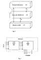
- FIG. 1shows a cross sectional view of a first embodiment of an integrated circuit that can be selectably fabricated as either an FPGA or an ASIC.
- a three-dimensional semiconductor device 100is shown.
- the device 100includes a first module layer 102 having a plurality of circuit blocks 104 embedded therein.
- the device 100also includes a second module layer 106 formed substantially above the first module layer 102 .
- One or more configuration circuits 108are formed to store instructions to control a portion of the circuit blocks 104 .
- circuits 108are programmable to build FPGA products.
- circuits 108are wire connections to build ASIC products.
- wiring/routing circuits 112are formed on a third layer 110 above the second layer 106 . Circuits 112 connect to both circuits 104 and 108 to complete the functionality of the PLD.
- FIG. 2shows a cross sectional view of a second embodiment of an integrated circuit that can be selectably fabricated as either an FPGA or an ASIC.
- a three-dimensional semiconductor device 120is shown.
- the device 120includes a first module layer 122 having a plurality of circuit blocks 124 embedded therein.
- the device 120also includes a second module layer 126 formed substantially above the first module layer 122 that includes wiring and/or routing circuitry 128 , and a third module layer 130 formed substantially above the second module layer 126 that includes configuration circuits 132 .
- circuits 132are programmable to build FPGA products.
- circuits 132are wire connections to build ASIC products.
- the wiring/routing circuitry 128is electrically connected to the circuit blocks 124 and to configuration circuits 132 in a third module layer 130 .
- the configuration circuits 132store instructions to control a portion of the circuit blocks 124 .
- FIG. 3shows a third embodiment which is substantially similar to the embodiment of FIG. 2 .
- a fourth layer 140 having wiring/routing circuitry 142is position above the third layer 130 .
- the wiring/routing circuitry 142is electrically connected to one of the following: one or more circuit blocks 124 , one or more wiring/routing circuitry 128 , and one or more configuration circuits 132 .
- FIG. 4shows one implementation where the configuration memory element is SRAM.
- silicon transistors 150are deposited on a substrate.
- a module layer of removable SRAM memory cells 152are positioned above the silicon transistors 150 , and a module layer of interconnect wiring or routing circuit 154 is formed above the removable memory cells 152 .
- SRAM cells 152are programmable to build FPGA products.
- cells 152are replaced with wire connections to build ASIC products.
- the designadheres to a hierarchical layout structure. As shown in FIG. 4 , the SRAM cell module is sandwiched between the single crystal device layers below and the metal layers above electrically connecting to both. It also provides through connections “A” for the lower device layers to upper metal layers.
- the SRAM modulecontains no switching electrical signal routing inside the module. All such routing is in the layers above and below. Most of the programmable element configuration signals run inside the module. Upper layer connections to SRAM module “C” are minimized to Power, Ground and high drive data wires. Connections “B” between SRAM module and single crystal module only contain logic level signals and replaced later by Vcc and Vss wires to build the ASIC. Most of the replaceable programmable elements and its configuration wiring is in the “replaceable module” while all the devices and end ASIC wiring is outside the “replaceable module”. In other embodiments, the replaceable module could exist between two metal layers or as the top most layer satisfying the same device and routing constraints.
- Fabrication of the ICalso follows a modularized device formation. Formation of transistors 150 and routing 154 is by utilizing a standard logic process flow used in the ASIC fabrication. Extra processing steps used for memory element 152 formation are inserted into the logic flow after circuit layer 150 is constructed. A fill disclosure of the vertical integration of the TFT module using extra masks and extra processing is in the co-pending incorporated by reference applications discussed above.
- the custom wire connectionscan be combined with the contact in module- 1 and metal- 1 in module- 2 processing.
- the custom wire connectionscan be an extra metal- 1 , via- 1 insertion compatible with logic processing. Removal of the SRAM module provides a low cost standard logic process for the final ASIC construction with the added benefit of a smaller die size. The design timing is unaffected by this migration as lateral metal routing and silicon transistors are untouched. Software verification and the original FPGA design methodology provide a guaranteed final ASIC solution to the user. A fill disclosure of the ASIC migration from the original FPGA is provided in the body of this discussion.
- the third module layeris formed substantially above the first and second module layers, wherein interconnect and routing signals are formed to connect the circuit modules within the first and second module layers.
- the third module layercan be formed substantially below the first and second module layer with the interconnect and routing signals formed to connect the circuit modules within the first and second module layers.
- the third and fourth module layerspositioned above and below the second module layer respectively, wherein the third and fourth module layers provide interconnect and routing signals to connect the circuit modules within the first and second module layers.
- a first module layeris fabricated having a plurality of circuit blocks formed on a first plane.
- the programmable multi-dimensional semiconductor devicealso includes a second module layer formed on a second plane.
- a plurality of configuration circuitsis then formed to store instructions to control a portion of the circuit modules.
- a programmable logic devicein another embodiment, includes one or more digital circuits formed on a substrate; and a non-planar circuit electrically coupled to the digital circuits, the non-planar circuit being either a memory constructed to store data to define the logic outputs of the digital circuits to fabricate a field programmable gate array (FPGA) or a conductive pattern constructed to define the logic outputs of the digital circuits to fabricate an application specific integrated circuit (ASIC), wherein the memory and the conductive pattern options have substantially matching functionality timing characteristics.
- FPGAfield programmable gate array
- ASICapplication specific integrated circuit
- the design/conversion of the FPGA to the ASICis explained next The larger and very complex FPGA designs are done with computer-aided design (CAD) tools.
- a design specificationis converted to a logical entry format for a Design Entry CAD tool.
- the abstract logic functionsare described using Hardware Description Language (HDL, VHDL) or Schematic Diagrams.
- HDL, VHDLHardware Description Language
- the design entryis compiled to extract the netlist. This netlist is used to synthesize the logic to be placed in the FPGA. Design capture so far is independent of the FPGA platform.
- a customized Place and Route (fitter) software toolis used to select the logic gates and to make the required connections in a chosen FPGA.
- the design placed and routed inside the FPGAis simulated using test vectors to verify the performance and functionality.
- the optimized design databasespecifies how the FPGA programmable resources are utilized to achieve the original design objectives.
- a configuration bitstreamis generated by a tool commonly referred to as a bitstream compiler. All the logic and routing customization specific to the design is contained in this bitstream, which is a binary representation of every single configuration device in the FPGA. This is also referred to as a bitmap when the bitstream is mapped to the image of configuration elements.
- the defining binary data in the bitstreamrepresent the ON/OFF states of the configurable switches that control logic blocks, IO blocks and interconnection in the FPGA.
- the configuration bitstreameither may be downloaded to the logic array thereby configuring the device or the bitstream may be saved onto disk.
- the FPGAcontains non volatile memory elements, a programmer is used to program the bitmap into the device.
- Some non volatile memory (NVM) elementssuch as EEPROM and Flash lend to in system programmability (ISP), allowing programming inside the design board via JTAG instructions.
- ISPsystem programmability
- SRAM based FPGAallow ISP, but need a NVM content outside the device to hold the bitstream.
- These B contactsrepresent configuration element control of the logic blocks. There is a one to one matching between these B contacts and the bitmap generated for the design, as every configuration element is represented in both.
- Bitstream onesrepresent B contacts at Vcc, while bitstream zeros represent B contacts at Vss.
- the bitstreamcan be automatically mapped to contact B file to convert those to Vcc and Vss hard connections.
- the contacts Bare in the CAD database that generates the physical mask for wafer processing. This technique provides an error free software conversion of the bitstream to a had-wire mask.
- Vcc and Vss resourcesBy appropriate pre-allocation of Vcc and Vss resources above the B contacts, one could conceivably generate the ASIC with only one custom mask, a considerable savings in expensive mask costs. All the C contacts in the hard mask are simply omitted as no configuration elements exist, while all the A contacts are retained.
- the conversiondoes not result in a new placement and routing configuration that is different from the previous FPGA design.
- the conversiondoes not result in a change to the logic gates in module layer- 1 or the lateral wire routing in module layer- 3 .
- the vertical contact height changeis negligible in the gate and wire delay components of logic propagation.
- Logic gate timingis not affected by control options between SRAM output or Vcc/Vss. The timing is maintained identical in this FPGA to ASIC conversion. Furthermore, this conversion can be made by the FPGA supplier, with no engineering overhead, saving valuable design resources at both end user and manufacturing sites.
- the final hard mask ASIChas no soft errors (no SRAM bits to flip), better reliability as fewer processing steps and fewer hard wires (one connection to replace 6-transistors) are used, and provide a secure environment against “bitstream piracy”—a technique of stealing designs by extracting the bitstream from FPGAs.
- circuit blocks 104the configuration circuit 108 , and the wiring and/or routing circuit 112 in FIG. 1 are detailed.
- circuit blocks 104A variety of digital or analog circuits can be used in circuit blocks 104 . These circuit blocks include programmable logic blocks to allow user customization of logic. In one embodiment, programmable logic blocks are provided to respond to input data signals. The programmable logic blocks develop corresponding complete or partial output logic signals. Registers are used to store the output logic signals and either outputting them to output terminals or returning them as inputs to additional programmable logic blocks. The registers themselves can be programmable, allowing those to be configured such as T flip-flops, JK flip-flops, or any other register. The logic blocks may contain no registers, or the registers may be programmed to be by-passed to facilitate combinational logic implementation.
- the programmable logic blockcan be selected from one of a pass gate logic, a multiplexer logic, a truth table logic, or an AND/OR logic.
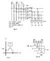
- FIG. 5shows an exemplary AND-OR PLD Architecture.
- AND and OR arrays 202 and 204contain user configurable programmable elements.
- FIG. 6shows an exemplary AND-OR array gate realization of a three input, four P-term, four output PLD.
- the AND and the OR array 210 - 212are shown programmed to a specific pattern.
- the circuit block 104contains a RAM/ROM logic block consisting of “logic element tree” or “P-Term logic array” blocks that perform logic functions.
- FIG. 7shows one such NAND EEPROM implementation of a P-Term in NAND-NOR logic array
- FIG. 8shows the same P-term configuration for either SRAM, or hard-wired PLD architectures.
- FIG. 7shows two mirrored outputs P 1 and P 2 .
- an AND gate 232receives signals from pass transistors 222 , 224 , 228 and 230 .
- the pass transistor 222is controlled by block 220 shown in the dashed circle, while the pass transistor 228 is controlled by block 226 shown inside the dashed circle.
- the upper half of FIG. 8includes an AND gate 252 that receives inputs from pass transistors 242 , 244 , 248 and 250 , respectively.
- FIG. 9shows an exemplary pass-gate logic 260 connecting one input to one output
- the NMOS pass gate voltage level S 0determines an ON and OFF connection.
- OI 0 *S 0 +I 1 *S 1 +I 2 *S 2 +I 3 *S 3 .
- the MUXis constructed by combining four NMOS pass gate logic elements 280 - 286 shown in FIG. 9 .
- the truth table logic statesare represented by S 0 , S 1 , S 2 and S 3 .
- the realizationis done through six inverters collectively designated 250 and eight pass transistors collectively designated 260 .
- Logic statesare stored in 4 programmable registers.
- FIG. 12shows a logic tree constructed with five 2-input truth table logic blocks 320 - 328 to perform a full four input truth table.
- a four input truth tablehas 16 possible logic states S 0 , S 1 , . . . , S 15 .
- this logic tree constructionrequires 2 N logic states, and 2 (N-1) branches in the logic tree.
- N-1branches in the logic tree.
- a full truth table realizationis less efficient compared to a partial product term AND-OR array realization.
- the programmable logic blockcan be a programmable microprocessor block.
- the microprocessorcan be selected from third party IP cores such as: 8051, Z80, 68000, MIPS, ARM, and PowerPC. These microprocessor architectures include superscalar, Fine Grain Multi-Threading (FGMT) and Simultaneous Multi-Threading (SMT) that support Application Specific Packet Processing (ASPP) routines.
- FGMTFine Grain Multi-Threading
- SMTSimultaneous Multi-Threading
- APNApplication Specific Packet Processing
- PNIProgrammable Network Interface
- the processorcan contain hardware and software configurability. Hardware upgradeability can be greatly enhanced in microprocessors embedded in PLD's by making use of the available logic content of the PLD device.
- Programmable featurescan include varying processor speed, cache memory system and processor configuration, enhancing the degree of Instruction Level Parallelism (ILP), enhancing Thread level parallelism (TLP). Such enhancements allow the user to optimize the core processor to their specific application. Cache parameters such as access latency, memory bandwidth, interleaving and partitioning are also programmable to further optimize processor performance and minimize cache hit miss rates.
- the processor blockcan be a Very Long Instruction Word (VLIW) processor to handle multimedia applications.
- VLIWVery Long Instruction Word
- the processor blockcan include a cache controller to implement a large capacity cache as compared with an internal cache.
- the programmable logic blockcan also contain a digital signal processor (DSP), which is a special purpose processor designed to optimize performance for very high speed digital signal processing encountered in wireless and fiber-optic networks.
- DSPdigital signal processor
- the DSP applicationscan include programmable content for cache partitioning, digital filters, image processing and speech recognition blocks. These real-time DSP applications contain high interrupt rates and intensive numeric computations best handled by hardware blocks. In addition, the applications tend to be intensive in memory access operations, which may require the input and output of large quantities of data
- the DSP cache memorymay be configured to have a “Harvard” architecture with separate, independent program and data memories so that the two memories may be accessed simultaneously.
- This architecturepermits an instruction and an operand to be fetched from memory in a single clock cycle.
- a modified Harvard architectureutilizes the program memory for storing both instructions and operands to achieve full memory utilization.
- the program and data memoriesare often interconnected with the core processor by separate program and data buses.
- conflictsmay arise in fetching data with the next instruction. Such conflicts have been resolved in prior art for DSPs by providing an instruction cache to store conflicting instructions for subsequent program execution.
- programmable logic blockcan contain software programmability. These software functions are executed in DSP, ARM, or MIPS type inserted IP cores, or an external host CPU. Accelerators connected by a configurable SRAM switching matrix enhance the computation power of the processors.
- the microprocessorhas local permanent SRAM memory to swap, read, and write data.
- the switch matrixis pre-designed to offer both hard-wire and programmable options in the final ASIC.
- the circuit block 104can be a functional block that performs well-defined, commonly-needed function, such as special D/A or A/D converter, standard bus interface, or such block that implements special algorithms such as MPEG decode.
- the special algorithms implementedcan be hardware versions of software. For example, algorithms relating to digital radio or cellular telephone such as WCDMA signal processing can be implemented by the functional block.
- Other functional blocksinclude PCI, mini-PCI, USB, UART blocks that can be configured by specifying the SRAM logic blocks.
- the circuit block 104can be memory such as a register file, cache memory, static memory, or dynamic memory.
- a register fileis an array of latches that operate at high speed. This register length counter may be programmable by the user.
- a cache memoryhas a high access throughput, short access latency and a smaller capacity as compared with main memory.
- the cache memorymay be programmable to partition between the different requirements of the system design. One such need is the division between L1 and L2 cache requirements for networking applications.
- the memorycan also be static random access memory or (SRAM) device with an array of single port, or multi-port addressable memory cells. Each cell includes a four transistor flip-flop and access transistors that are coupled to input/output nodes of the flip-flop.
- SRAMstatic random access memory
- Datais written to the memory cell by applying a high or low logic level to one of the input/output nodes of the flip-flop through one of the access transistors. When the logic level is removed from the access transistor, the flip-flop reins this logic level at the input/output node. Data is read out from the flip-flop by turning on the access transistor.
- the memorycan also be dynamic random access memory (DRAM).
- DRAMdynamic random access memory
- a DRAM cellconsists of one transistor and a capacitor. A word line turns on/off the transistor at the time of reading/writing data stored in the capacitor, and the bit line is a data input/output path. DRAM data is destroyed during read, and refresh circuitry is used to continually refresh the data. Due to the low component count per bit, a high density memory device is achieved.
- the circuit block 104can be an intellectual property (“IP”) core which is reusable for licensing from other companies or which is taken from the same/previous design.
- IPintellectual property
- core-based designindividual cores may be developed and verified independently as stand-alone modules, particularly when IP core is licensed from external design source.
- IP blocksconnect via a programmable switching matrix to each other and other programmable logic.
- the hardware logic block insertion to any position in a logic sequenceis done through the configurable logic matrix.
- These hardware logic blocksoffer a significant gate count reduction on high gate count frequently used logic functions, and the user does not require generic “logic element” customization. In both cases, the user saves simulation time, minimize logic gate count, improve performance, reduce power consumption and reduce product cost with predefined IP blocks.
- the switch matrixis replaced by hard-wires in the final ASIC.
- the circuit blocks 104can also be an array of programmable analog blocks.
- the analog blocksinclude programmable PLL, DLL, ADC and DAC.
- each blockcontains an operational amplifier, multiple programmable capacitors, and switching arrangements for connecting the capacitors in such as a way as to perform the desired function.
- Switched capacitor filterscan also be used to achieve an accurate filter specification through a ratio of capacitors and an accurate control of the frequency of a sampling clock.
- Multiple PLL'scan be programmed to run at different frequencies on the same chip to facilitate SoC applications requiring more than one clock frequency.
- the circuit blocks 104also contain data fetch and data write circuitry required to configure the configuration circuits 108 . This operation may be executed by a host CPU residing in the system, or the PLD device itself. During power up, these circuits initialize and read the configuration data from an outside source, either in serial mode or in parallel mode. The data is stored in a predefined word length locally and written to the configurability allocation. The programmed configuration data is verified against the locally stored data and a programming error flag is generated if there is a mismatch. These circuits are redundant in the conversion of the PLD to an ASIC. However, these circuits are used in both FPGA and ASIC for test purposes, and has no cost penalty. A pin-out option has a “disable” feature to disconnect them for the customer use in the FPGA and ASIC.
- Configuration circuits 108provide active circuit control over digital circuits 104 .
- One embodiment of the configuration circuitincludes an array of memory elements. The user configuration of this memory amounts to a specific bitmap of the programmable memory in a software representation.
- Suitable memory elementsinclude volatile or non volatile memory elements.
- NVMnon-volatile memory
- configurable datais held in one of metal link fuse, anti-fuse, EPROM, Flash, EEPROM memory element, or ferro-electric elements. The first two are one time programmable (OTP), while the last four can be programmed multiple times.
- OTPone time programmable
- Flash & EEPROM'slend to in-system programmability (ISP).
- the configurable data storagecan be SRAM cells or DRAM cells. With DRAM cells, the data requires constant refresh to prevent losses from leakages. Additionally, one or more redundant memory cells controlling the same circuit block can be used to enhance device yield.
- the components of the memory element arraycan be a resistor, capacitor, transistor or a diode.
- a memory elementcan be formed using thin film deposition.
- the memory elementcan be a thin film resistor, thin film capacitor, thin film transistor (TFT) or a thin film diode or a group of thin film devices connected to form an SRAM cell.
- An exemplary 6T SRAM cellshown in FIG. 13 , needs no high voltage capability, nor added process complexity.
- the cell of FIG. 13has two back-to-back inverters 350 - 352 whose access is controlled by pass transistors 354 - 356 .
- R-load & Thin Film Transistor (TFT) load PMOS based SRAM cellscan be used for PLDs and FPGAs.
- TFTThin Film Transistor
- Pass gate transistor 360 logic controlled by SRAMis shown in FIG. 14 .
- the memory cell(such as the cell of FIG. 13 ) drives the pass transistor 360 to e affect an outcome.
- a 5 ⁇ 6-switch point matrix 370 controlled by 30-SRAM cells coupled to 30-NMOS pass gatesis shown in FIG. 15 .
- FIG. 16shows the NMOS pass gate 360 logic controlled by the SRAM in FIG. 14 converted to hard-wire logic.
- a contact 362connected to Vcc (logic 1 ) or Vss (logic 0 ) depending on the SRAM logic content, replace the SRAM cell.
- the SRAM logic mapping to hard wire connectionsare automatic and done by a software program that is verifiable against the bit-map.
- FIG. 17shows the 5 ⁇ 6-switch point matrix 370 hard-wired by replacing the SRAM bits that control NMOS gates with hard-wires to Vcc or Vss.
- the bubblemay represent either SRAM or hard-wire Vcc or Vss control on NMOS pass gates.
- contact or no contact between the two metal lines in FIG. 15directly replaces the programmable element and there is no NMOS pass-gate needed.
- the P-Term logicbuilds the core of PLD's and complex PLD's (CPLD's) that use AND-OR blocks 202 - 204 (or equivalent NAND-NOR type logic functions) as shown in the block diagram of FIG. 5 and one expansion is shown in FIG. 6 with and gates 210 and or gates 212 .
- Gate implementation of two inputs (I 1 , I 2 ) and two P-terms (P 1 , P 2 ) NAND functioncan be single poly EEPROM bits as shown in FIG. 10 .
- the dotted circlecontains the charge trapping floating gate, the programming select transistor, tunneling diode, a control gate capacitor and programming access nodes.
- the SRAM cellreplaces that entire circle in this invention as detailed next.
- the SRAM NAND-NOR array (also AND-OR array) replacementhas not been realized in prior art as SRAM cells require Nwell & Pwell regions that consume large silicon area to prevent latch-up.
- the SRAM in TFTdo not have well related constraints as NMOS and PMOS bodies are isolated from each other. Keeping the two pass gates in silicon layers and moving SRAM to TFT layers allow P-Term logic implementation with SRAM cells and subsequent replacement with hard-wires. In TFT SRAM conversion to final ASIC, the bubble on NMOS gate becomes a hard-wire connection to Vcc or Vss.
- the length of input and output wires, and the drive on NMOS pass gates and logic gate delaysdetermine the overall PLD delay timing, independent of the SRAM cell parameters.
- the chip X,Y dimensionsare reduced over 20% to 50% compared to traditional SRAM FPGA's, providing a faster logic evaluation time.
- removal of SRAM cell laterdoes not alter lateral wire length, wire loading and NMOS pass gate characteristic.
- the vertical dimension change in eliminating the memory moduleis negligible compared to the lateral dimension of the ASIC, and has no impact on timing. This allows maintaining identical timing between the FPGA and ASIC implementations with and without the *SRAM cells.
- the final ASIC with smaller die size and no SRAM elementshave superior reliability, similar to an ASIC, leading to lower board level burn-in and field failures compared to PLD's and FPGA's in use today.
- the wiring and/or routing circuit 112connects each logic block to each other logic block.
- the wiring/routing circuitallows a high degree of routing flexibility per silicon area consumed and uniformly fast propagation of signals, including high-fanout signals, throughout the device.
- the wiring modulemay contain one or many levels of metal interconnects.
- FIG. 15One embodiment of a switch matrix is a 6 ⁇ 5 programmable switch-matrix with 30 SRAM bits (or 30 Anti-fuses, or 30 fuses), shown in FIG. 15 .
- the box in FIG. 14contains the SRAM cell shown inside dotted box of FIG. 14 , where the pass gate makes the connection between the two wires, and the SRAM bit holds the configuration data
- the wire connection in circuit 112occurs via a pass transistor located in circuit 104 controlled by an SRAM cell in circuit 108 .
- a permanent non-volatile memory block located in the systemloads the correct configuration data into SRAM cells.
- the boxsimply represents the programmable element in circuit 108 between the two wires in circuit 112 . During the ASIC conversion this link is replaced with an open or short between the wires.
- Another embodimentprovides short interconnect segments that could be joined to each other and to input and output terminals of the logic blocks at programmable interconnection points.
- direct connections to adjacent logic blockscan be used to increase speed.
- longer linesare used Segmented interconnect structures with routing lines of varied lengths can be used.
- a hierarchical interconnect structureprovides lines of short lengths connectable at boundaries to lines of longer lengths extending between the boundaries, and larger boundaries with lines of even longer length extending between those boundaries.
- the routing circuitcan connect adjacent logic blocks in two different hierarchical blocks differently than adjacent logic blocks in the same hierarchical block.
- a tile-based interconnect structurecan be used where lines of varying lengths in which each tile in a rectangular array may be identical to each other tile.
- the interconnect linescan be separated from the logic block inputs by way of a routing matrix, which gives each interconnect line more flexible access to the logic block inputs.
- the interconnect routingis driven by programmable buffers. Long wire lengths can be sub-divided into smaller length segments with smaller buffers to achieve a net reduction in the overall wire delay, and to obtain predictable tiring in the logic routing of the PLD.
- one or more digital circuitscan be formed on a substrate.
- the processselectively fabricates either a memory circuit or a conductive pattern substantially above the digital circuits to control portion of digital circuits.
- the processfabricates an interconnect and routing layer substantially above the digital circuits and memory circuits to connect digital circuits and one of the memory circuit or the conductive pattern.
- the processcan be modified to fabricate a generic field programmable gate array (FPGA) with the constructed memory circuit or an application specific integrated circuit (ASIC) with the constructed conductive pattern.
- FPGAfield programmable gate array
- ASICapplication specific integrated circuit
- Multiple ASICscan be fabricated with different variations of conductive patterns.
- the memory circuit and the conductive patternhave one or more substantially matching circuit characteristics. In this case, timing characteristics substantially unchanged by the circuit control option.
- the processthus fabricates a programmable logic device by constructing digital circuits on a substrate; and constructing a non-planar circuit on the substrate after constructing the digital circuits, the non-planar circuit being either a memory deposited to store data to configure the digital circuits to form a field programmable gate array (FPGA) or a conductive pattern deposited to hard-wire the digital circuits to form an application specific integrated circuit (ASIC), wherein the deposited memory and the conductive pattern have substantially matching timing characteristics.
- the hard-wire ASIC optionmay be incorporated into the digital circuit layer 100 .
- the hard-wire ASIC optionis incorporated into the routing layer 110 .
Landscapes
- Engineering & Computer Science (AREA)
- Computer Hardware Design (AREA)
- Physics & Mathematics (AREA)
- Theoretical Computer Science (AREA)
- General Engineering & Computer Science (AREA)
- General Physics & Mathematics (AREA)
- Geometry (AREA)
- Evolutionary Computation (AREA)
- Mathematical Physics (AREA)
- Computing Systems (AREA)
- Computer Networks & Wireless Communication (AREA)
- Design And Manufacture Of Integrated Circuits (AREA)
- Logic Circuits (AREA)
Abstract
Description
F=/A*/B*S0+/A*B*S1+A*/B*S2+A*B*S3 (/Ameans notA).
The truth table logic states are represented by S0, S1, S2 and S3. The realization is done through six inverters collectively designated250 and eight pass transistors collectively designated260. Logic states are stored in 4 programmable registers.
Claims (17)
Priority Applications (6)
| Application Number | Priority Date | Filing Date | Title |
|---|---|---|---|
| US11/645,313US7627848B2 (en) | 2002-07-08 | 2006-12-26 | Bit stream compatible FPGA to MPGA conversions |
| US11/712,380US7673273B2 (en) | 2002-07-08 | 2007-03-01 | MPGA products based on a prototype FPGA |
| US12/104,377US8499269B2 (en) | 2002-07-08 | 2008-04-16 | Timing exact design conversions from FPGA to ASIC |
| US13/411,486USRE45110E1 (en) | 2006-03-20 | 2012-03-02 | MPGA products based on a prototype FPGA |
| US13/953,666US9547736B2 (en) | 2002-07-08 | 2013-07-29 | Timing exact design conversions from FPGA to ASIC |
| US15/407,242US10339245B2 (en) | 2002-07-08 | 2017-01-16 | Timing exact design conversions from FPGA to ASIC |
Applications Claiming Priority (6)
| Application Number | Priority Date | Filing Date | Title |
|---|---|---|---|
| US39376302P | 2002-07-08 | 2002-07-08 | |
| US39707002P | 2002-07-22 | 2002-07-22 | |
| US10/267,511US6747478B2 (en) | 2002-07-08 | 2002-10-08 | Field programmable gate array with convertibility to application specific integrated circuit |
| US10/825,194US6992503B2 (en) | 2002-07-08 | 2004-04-16 | Programmable devices with convertibility to customizable devices |
| US11/384,116US7356799B2 (en) | 2002-07-08 | 2006-03-20 | Timing exact design conversions from FPGA to ASIC |
| US11/645,313US7627848B2 (en) | 2002-07-08 | 2006-12-26 | Bit stream compatible FPGA to MPGA conversions |
Related Parent Applications (1)
| Application Number | Title | Priority Date | Filing Date |
|---|---|---|---|
| US11/384,116ContinuationUS7356799B2 (en) | 2002-07-08 | 2006-03-20 | Timing exact design conversions from FPGA to ASIC |
Related Child Applications (2)
| Application Number | Title | Priority Date | Filing Date |
|---|---|---|---|
| US11/712,380Continuation-In-PartUS7673273B2 (en) | 2002-07-08 | 2007-03-01 | MPGA products based on a prototype FPGA |
| US12/104,377ContinuationUS8499269B2 (en) | 2002-07-08 | 2008-04-16 | Timing exact design conversions from FPGA to ASIC |
Publications (2)
| Publication Number | Publication Date |
|---|---|
| US20070103192A1 US20070103192A1 (en) | 2007-05-10 |
| US7627848B2true US7627848B2 (en) | 2009-12-01 |
Family
ID=33102109
Family Applications (8)
| Application Number | Title | Priority Date | Filing Date |
|---|---|---|---|
| US10/825,194Expired - LifetimeUS6992503B2 (en) | 2002-07-08 | 2004-04-16 | Programmable devices with convertibility to customizable devices |
| US10/864,092Expired - LifetimeUS7205589B2 (en) | 2002-07-08 | 2004-06-08 | Semiconductor devices fabricated with different processing options |
| US11/384,116Expired - LifetimeUS7356799B2 (en) | 2002-07-08 | 2006-03-20 | Timing exact design conversions from FPGA to ASIC |
| US11/645,313Expired - Fee RelatedUS7627848B2 (en) | 2002-07-08 | 2006-12-26 | Bit stream compatible FPGA to MPGA conversions |
| US11/801,738Expired - Fee RelatedUS7759705B2 (en) | 2002-07-08 | 2007-05-11 | Semiconductor devices fabricated with different processing options |
| US12/104,377Expired - Fee RelatedUS8499269B2 (en) | 2002-07-08 | 2008-04-16 | Timing exact design conversions from FPGA to ASIC |
| US13/953,666Expired - Fee RelatedUS9547736B2 (en) | 2002-07-08 | 2013-07-29 | Timing exact design conversions from FPGA to ASIC |
| US15/407,242Expired - Fee RelatedUS10339245B2 (en) | 2002-07-08 | 2017-01-16 | Timing exact design conversions from FPGA to ASIC |
Family Applications Before (3)
| Application Number | Title | Priority Date | Filing Date |
|---|---|---|---|
| US10/825,194Expired - LifetimeUS6992503B2 (en) | 2002-07-08 | 2004-04-16 | Programmable devices with convertibility to customizable devices |
| US10/864,092Expired - LifetimeUS7205589B2 (en) | 2002-07-08 | 2004-06-08 | Semiconductor devices fabricated with different processing options |
| US11/384,116Expired - LifetimeUS7356799B2 (en) | 2002-07-08 | 2006-03-20 | Timing exact design conversions from FPGA to ASIC |
Family Applications After (4)
| Application Number | Title | Priority Date | Filing Date |
|---|---|---|---|
| US11/801,738Expired - Fee RelatedUS7759705B2 (en) | 2002-07-08 | 2007-05-11 | Semiconductor devices fabricated with different processing options |
| US12/104,377Expired - Fee RelatedUS8499269B2 (en) | 2002-07-08 | 2008-04-16 | Timing exact design conversions from FPGA to ASIC |
| US13/953,666Expired - Fee RelatedUS9547736B2 (en) | 2002-07-08 | 2013-07-29 | Timing exact design conversions from FPGA to ASIC |
| US15/407,242Expired - Fee RelatedUS10339245B2 (en) | 2002-07-08 | 2017-01-16 | Timing exact design conversions from FPGA to ASIC |
Country Status (1)
| Country | Link |
|---|---|
| US (8) | US6992503B2 (en) |
Cited By (7)
| Publication number | Priority date | Publication date | Assignee | Title |
|---|---|---|---|---|
| US8001537B1 (en)* | 2005-12-05 | 2011-08-16 | Altera Corporation | Method and apparatus for compiling programmable logic device configurations |
| US8875080B1 (en)* | 2013-12-04 | 2014-10-28 | Baysand Inc. | Programmable macros for metal/via programmable gate array integrated circuits |
| US20170124241A1 (en)* | 2002-07-08 | 2017-05-04 | Callahan Cellular L.L.C. | Timing exact design conversions from fpga to asic |
| US9666248B1 (en)* | 2015-10-16 | 2017-05-30 | Xilinx, Inc. | Secure configuration readback for programmable logic devices |
| US10304854B2 (en) | 2007-11-19 | 2019-05-28 | Callahan Cellular L.L.C. | Pads and pin-outs in three dimensional integrated circuits |
| US10447272B2 (en) | 2002-07-08 | 2019-10-15 | Callahan Cellular L.L.C. | Three dimensional integrated-circuits |
| US10594320B2 (en) | 2003-12-04 | 2020-03-17 | Callahan Cellular L.L.C. | Programmable structured arrays |
Families Citing this family (281)
| Publication number | Priority date | Publication date | Assignee | Title |
|---|---|---|---|---|
| KR100516693B1 (en)* | 2003-04-02 | 2005-09-22 | 주식회사 하이닉스반도체 | Non-volatile programmable logic circuit |
| US20040004251A1 (en)* | 2002-07-08 | 2004-01-08 | Madurawe Raminda U. | Insulated-gate field-effect thin film transistors |
| US7129744B2 (en)* | 2003-10-23 | 2006-10-31 | Viciciv Technology | Programmable interconnect structures |
| US7673273B2 (en) | 2002-07-08 | 2010-03-02 | Tier Logic, Inc. | MPGA products based on a prototype FPGA |
| US7064579B2 (en)* | 2002-07-08 | 2006-06-20 | Viciciv Technology | Alterable application specific integrated circuit (ASIC) |
| US6747478B2 (en)* | 2002-07-08 | 2004-06-08 | Viciciv | Field programmable gate array with convertibility to application specific integrated circuit |
| US7812458B2 (en)* | 2007-11-19 | 2010-10-12 | Tier Logic, Inc. | Pad invariant FPGA and ASIC devices |
| US20050116738A1 (en)* | 2003-12-01 | 2005-06-02 | Lsi Logic Corporation | Integrated circuits, and design and manufacture thereof |
| KR100564611B1 (en)* | 2004-02-14 | 2006-03-29 | 삼성전자주식회사 | Hard disk drive buffer structure |
| US7193440B1 (en)* | 2004-02-14 | 2007-03-20 | Herman Schmit | Configurable circuits, IC's, and systems |
| US7425841B2 (en) | 2004-02-14 | 2008-09-16 | Tabula Inc. | Configurable circuits, IC's, and systems |
| EP1721403A2 (en)* | 2004-03-03 | 2006-11-15 | Aware, Inc. | Impulse noise management |
| US7489164B2 (en)* | 2004-05-17 | 2009-02-10 | Raminda Udaya Madurawe | Multi-port memory devices |
| US7167026B2 (en)* | 2004-06-18 | 2007-01-23 | Nantero, Inc. | Tri-state circuit using nanotube switching elements |
| US7317331B2 (en) | 2004-11-08 | 2008-01-08 | Tabula, Inc. | Reconfigurable IC that has sections running at different reconfiguration rates |
| US7230869B1 (en) | 2005-03-15 | 2007-06-12 | Jason Redgrave | Method and apparatus for accessing contents of memory cells |
| US20060242611A1 (en)* | 2005-04-07 | 2006-10-26 | Microsoft Corporation | Integrating programmable logic into personal computer (PC) architecture |
| US8044437B1 (en)* | 2005-05-16 | 2011-10-25 | Lsi Logic Corporation | Integrated circuit cell architecture configurable for memory or logic elements |
| WO2007130919A2 (en)* | 2006-05-01 | 2007-11-15 | The Regents Of The University Of California | Nano-electro-mechanical memory cells and devices |
| US20080024165A1 (en)* | 2006-07-28 | 2008-01-31 | Raminda Udaya Madurawe | Configurable embedded multi-port memory |
| JP2008078363A (en)* | 2006-09-21 | 2008-04-03 | Matsushita Electric Ind Co Ltd | Variable path wiring cell, semiconductor integrated circuit, design method thereof, and variable path wiring cell forming method |
| US8018248B2 (en)* | 2006-09-21 | 2011-09-13 | Quicklogic Corporation | Adjustable interface buffer circuit between a programmable logic device and a dedicated device |
| KR20090078790A (en)* | 2006-09-26 | 2009-07-20 | 샌드브리지 테크놀로지스, 인코포레이티드 | Software implementation of matrix inversion in a wireless communication system |
| US7671624B1 (en)* | 2006-10-10 | 2010-03-02 | Xilinx, Inc. | Method to reduce configuration solution using masked-ROM |
| US8629006B2 (en)* | 2006-12-05 | 2014-01-14 | Agate Logic, Inc. | Hybrid integrated circuits and their methods of fabrication |
| US7589555B1 (en)* | 2007-01-08 | 2009-09-15 | Altera Corporation | Variable sized soft memory macros in structured cell arrays, and related methods |
| US7535252B1 (en) | 2007-03-22 | 2009-05-19 | Tabula, Inc. | Configurable ICs that conditionally transition through configuration data sets |
| US8344755B2 (en) | 2007-09-06 | 2013-01-01 | Tabula, Inc. | Configuration context switcher |
| US7882453B2 (en)* | 2007-10-17 | 2011-02-01 | Rapid Bridge Llc | Semiconductor device metal programmable pooling and dies |
| US20090128189A1 (en)* | 2007-11-19 | 2009-05-21 | Raminda Udaya Madurawe | Three dimensional programmable devices |
| US7635988B2 (en)* | 2007-11-19 | 2009-12-22 | Tier Logic, Inc. | Multi-port thin-film memory devices |
| US7573294B2 (en)* | 2007-12-26 | 2009-08-11 | Tier Logic, Inc. | Programmable logic based latches and shift registers |
| US7573293B2 (en)* | 2007-12-26 | 2009-08-11 | Tier Logic, Inc. | Programmable logic based latches and shift registers |
| US7602213B2 (en)* | 2007-12-26 | 2009-10-13 | Tier Logic, Inc. | Using programmable latch to implement logic |
| US7795913B2 (en)* | 2007-12-26 | 2010-09-14 | Tier Logic | Programmable latch based multiplier |
| US8667437B2 (en)* | 2008-03-17 | 2014-03-04 | Xilinx, Inc. | Creating a standard cell circuit design from a programmable logic device circuit design |
| US8230375B2 (en) | 2008-09-14 | 2012-07-24 | Raminda Udaya Madurawe | Automated metal pattern generation for integrated circuits |
| US7834712B2 (en)* | 2008-10-09 | 2010-11-16 | Altera Corporation | Techniques for providing option conductors to connect components in an oscillator circuit |
| US8362482B2 (en) | 2009-04-14 | 2013-01-29 | Monolithic 3D Inc. | Semiconductor device and structure |
| US8378715B2 (en) | 2009-04-14 | 2013-02-19 | Monolithic 3D Inc. | Method to construct systems |
| US8427200B2 (en) | 2009-04-14 | 2013-04-23 | Monolithic 3D Inc. | 3D semiconductor device |
| US8754533B2 (en) | 2009-04-14 | 2014-06-17 | Monolithic 3D Inc. | Monolithic three-dimensional semiconductor device and structure |
| US8362800B2 (en) | 2010-10-13 | 2013-01-29 | Monolithic 3D Inc. | 3D semiconductor device including field repairable logics |
| US7986042B2 (en) | 2009-04-14 | 2011-07-26 | Monolithic 3D Inc. | Method for fabrication of a semiconductor device and structure |
| US9509313B2 (en) | 2009-04-14 | 2016-11-29 | Monolithic 3D Inc. | 3D semiconductor device |
| US9711407B2 (en) | 2009-04-14 | 2017-07-18 | Monolithic 3D Inc. | Method of manufacturing a three dimensional integrated circuit by transfer of a mono-crystalline layer |
| US8058137B1 (en) | 2009-04-14 | 2011-11-15 | Monolithic 3D Inc. | Method for fabrication of a semiconductor device and structure |
| US8373439B2 (en) | 2009-04-14 | 2013-02-12 | Monolithic 3D Inc. | 3D semiconductor device |
| US8405420B2 (en) | 2009-04-14 | 2013-03-26 | Monolithic 3D Inc. | System comprising a semiconductor device and structure |
| US8384426B2 (en)* | 2009-04-14 | 2013-02-26 | Monolithic 3D Inc. | Semiconductor device and structure |
| US8669778B1 (en) | 2009-04-14 | 2014-03-11 | Monolithic 3D Inc. | Method for design and manufacturing of a 3D semiconductor device |
| US9577642B2 (en) | 2009-04-14 | 2017-02-21 | Monolithic 3D Inc. | Method to form a 3D semiconductor device |
| US8395191B2 (en) | 2009-10-12 | 2013-03-12 | Monolithic 3D Inc. | Semiconductor device and structure |
| US8216902B2 (en)* | 2009-08-06 | 2012-07-10 | International Business Machines Corporation | Nanomesh SRAM cell |
| US10354995B2 (en) | 2009-10-12 | 2019-07-16 | Monolithic 3D Inc. | Semiconductor memory device and structure |
| US11018133B2 (en) | 2009-10-12 | 2021-05-25 | Monolithic 3D Inc. | 3D integrated circuit |
| US8450804B2 (en) | 2011-03-06 | 2013-05-28 | Monolithic 3D Inc. | Semiconductor device and structure for heat removal |
| US10043781B2 (en) | 2009-10-12 | 2018-08-07 | Monolithic 3D Inc. | 3D semiconductor device and structure |
| US10366970B2 (en) | 2009-10-12 | 2019-07-30 | Monolithic 3D Inc. | 3D semiconductor device and structure |
| US8476145B2 (en) | 2010-10-13 | 2013-07-02 | Monolithic 3D Inc. | Method of fabricating a semiconductor device and structure |
| US12027518B1 (en) | 2009-10-12 | 2024-07-02 | Monolithic 3D Inc. | 3D semiconductor devices and structures with metal layers |
| US8148728B2 (en) | 2009-10-12 | 2012-04-03 | Monolithic 3D, Inc. | Method for fabrication of a semiconductor device and structure |
| US10157909B2 (en) | 2009-10-12 | 2018-12-18 | Monolithic 3D Inc. | 3D semiconductor device and structure |
| US8536023B2 (en) | 2010-11-22 | 2013-09-17 | Monolithic 3D Inc. | Method of manufacturing a semiconductor device and structure |
| US10910364B2 (en) | 2009-10-12 | 2021-02-02 | Monolitaic 3D Inc. | 3D semiconductor device |
| US11984445B2 (en) | 2009-10-12 | 2024-05-14 | Monolithic 3D Inc. | 3D semiconductor devices and structures with metal layers |
| US8581349B1 (en) | 2011-05-02 | 2013-11-12 | Monolithic 3D Inc. | 3D memory semiconductor device and structure |
| US9099424B1 (en) | 2012-08-10 | 2015-08-04 | Monolithic 3D Inc. | Semiconductor system, device and structure with heat removal |
| US11374118B2 (en) | 2009-10-12 | 2022-06-28 | Monolithic 3D Inc. | Method to form a 3D integrated circuit |
| US8742476B1 (en) | 2012-11-27 | 2014-06-03 | Monolithic 3D Inc. | Semiconductor device and structure |
| US10388863B2 (en) | 2009-10-12 | 2019-08-20 | Monolithic 3D Inc. | 3D memory device and structure |
| US8492886B2 (en) | 2010-02-16 | 2013-07-23 | Monolithic 3D Inc | 3D integrated circuit with logic |
| US8373230B1 (en) | 2010-10-13 | 2013-02-12 | Monolithic 3D Inc. | Method for fabrication of a semiconductor device and structure |
| US9099526B2 (en) | 2010-02-16 | 2015-08-04 | Monolithic 3D Inc. | Integrated circuit device and structure |
| US8461035B1 (en) | 2010-09-30 | 2013-06-11 | Monolithic 3D Inc. | Method for fabrication of a semiconductor device and structure |
| US8026521B1 (en) | 2010-10-11 | 2011-09-27 | Monolithic 3D Inc. | Semiconductor device and structure |
| US8541819B1 (en) | 2010-12-09 | 2013-09-24 | Monolithic 3D Inc. | Semiconductor device and structure |
| JP5032611B2 (en)* | 2010-02-19 | 2012-09-26 | 株式会社東芝 | Semiconductor integrated circuit |
| US10217667B2 (en) | 2011-06-28 | 2019-02-26 | Monolithic 3D Inc. | 3D semiconductor device, fabrication method and system |
| US8642416B2 (en) | 2010-07-30 | 2014-02-04 | Monolithic 3D Inc. | Method of forming three dimensional integrated circuit devices using layer transfer technique |
| US9219005B2 (en) | 2011-06-28 | 2015-12-22 | Monolithic 3D Inc. | Semiconductor system and device |
| US9953925B2 (en) | 2011-06-28 | 2018-04-24 | Monolithic 3D Inc. | Semiconductor system and device |
| US8901613B2 (en) | 2011-03-06 | 2014-12-02 | Monolithic 3D Inc. | Semiconductor device and structure for heat removal |
| US8105885B1 (en) | 2010-08-06 | 2012-01-31 | Altera Corporation | Hardened programmable devices |
| WO2012047735A2 (en)* | 2010-09-29 | 2012-04-12 | The Regents Of The University Of California | In-place resynthesis and remapping techniques for soft error mitigation in fpga |
| US11482440B2 (en) | 2010-12-16 | 2022-10-25 | Monolithic 3D Inc. | 3D semiconductor device and structure with a built-in test circuit for repairing faulty circuits |
| US10497713B2 (en) | 2010-11-18 | 2019-12-03 | Monolithic 3D Inc. | 3D semiconductor memory device and structure |
| US8273610B2 (en) | 2010-11-18 | 2012-09-25 | Monolithic 3D Inc. | Method of constructing a semiconductor device and structure |
| US8163581B1 (en) | 2010-10-13 | 2012-04-24 | Monolith IC 3D | Semiconductor and optoelectronic devices |
| US12362219B2 (en) | 2010-11-18 | 2025-07-15 | Monolithic 3D Inc. | 3D semiconductor memory device and structure |
| US11600667B1 (en) | 2010-10-11 | 2023-03-07 | Monolithic 3D Inc. | Method to produce 3D semiconductor devices and structures with memory |
| US11018191B1 (en) | 2010-10-11 | 2021-05-25 | Monolithic 3D Inc. | 3D semiconductor device and structure |
| US11469271B2 (en) | 2010-10-11 | 2022-10-11 | Monolithic 3D Inc. | Method to produce 3D semiconductor devices and structures with memory |
| US11024673B1 (en) | 2010-10-11 | 2021-06-01 | Monolithic 3D Inc. | 3D semiconductor device and structure |
| US8114757B1 (en) | 2010-10-11 | 2012-02-14 | Monolithic 3D Inc. | Semiconductor device and structure |
| US10896931B1 (en) | 2010-10-11 | 2021-01-19 | Monolithic 3D Inc. | 3D semiconductor device and structure |
| US11315980B1 (en) | 2010-10-11 | 2022-04-26 | Monolithic 3D Inc. | 3D semiconductor device and structure with transistors |
| US11257867B1 (en) | 2010-10-11 | 2022-02-22 | Monolithic 3D Inc. | 3D semiconductor device and structure with oxide bonds |
| US10290682B2 (en) | 2010-10-11 | 2019-05-14 | Monolithic 3D Inc. | 3D IC semiconductor device and structure with stacked memory |
| US11227897B2 (en) | 2010-10-11 | 2022-01-18 | Monolithic 3D Inc. | Method for producing a 3D semiconductor memory device and structure |
| US11158674B2 (en) | 2010-10-11 | 2021-10-26 | Monolithic 3D Inc. | Method to produce a 3D semiconductor device and structure |
| US11605663B2 (en) | 2010-10-13 | 2023-03-14 | Monolithic 3D Inc. | Multilevel semiconductor device and structure with image sensors and wafer bonding |
| US10978501B1 (en) | 2010-10-13 | 2021-04-13 | Monolithic 3D Inc. | Multilevel semiconductor device and structure with waveguides |
| US11404466B2 (en) | 2010-10-13 | 2022-08-02 | Monolithic 3D Inc. | Multilevel semiconductor device and structure with image sensors |
| US11855114B2 (en) | 2010-10-13 | 2023-12-26 | Monolithic 3D Inc. | Multilevel semiconductor device and structure with image sensors and wafer bonding |
| US11133344B2 (en) | 2010-10-13 | 2021-09-28 | Monolithic 3D Inc. | Multilevel semiconductor device and structure with image sensors |
| US11984438B2 (en) | 2010-10-13 | 2024-05-14 | Monolithic 3D Inc. | Multilevel semiconductor device and structure with oxide bonding |
| US11869915B2 (en) | 2010-10-13 | 2024-01-09 | Monolithic 3D Inc. | Multilevel semiconductor device and structure with image sensors and wafer bonding |
| US11063071B1 (en) | 2010-10-13 | 2021-07-13 | Monolithic 3D Inc. | Multilevel semiconductor device and structure with waveguides |
| US11043523B1 (en) | 2010-10-13 | 2021-06-22 | Monolithic 3D Inc. | Multilevel semiconductor device and structure with image sensors |
| US12080743B2 (en) | 2010-10-13 | 2024-09-03 | Monolithic 3D Inc. | Multilevel semiconductor device and structure with image sensors and wafer bonding |
| US9197804B1 (en) | 2011-10-14 | 2015-11-24 | Monolithic 3D Inc. | Semiconductor and optoelectronic devices |
| US11929372B2 (en) | 2010-10-13 | 2024-03-12 | Monolithic 3D Inc. | Multilevel semiconductor device and structure with image sensors and wafer bonding |
| US12094892B2 (en) | 2010-10-13 | 2024-09-17 | Monolithic 3D Inc. | 3D micro display device and structure |
| US11694922B2 (en) | 2010-10-13 | 2023-07-04 | Monolithic 3D Inc. | Multilevel semiconductor device and structure with oxide bonding |
| US11164898B2 (en) | 2010-10-13 | 2021-11-02 | Monolithic 3D Inc. | Multilevel semiconductor device and structure |
| US11437368B2 (en) | 2010-10-13 | 2022-09-06 | Monolithic 3D Inc. | Multilevel semiconductor device and structure with oxide bonding |
| US11327227B2 (en) | 2010-10-13 | 2022-05-10 | Monolithic 3D Inc. | Multilevel semiconductor device and structure with electromagnetic modulators |
| US11163112B2 (en) | 2010-10-13 | 2021-11-02 | Monolithic 3D Inc. | Multilevel semiconductor device and structure with electromagnetic modulators |
| US8379458B1 (en) | 2010-10-13 | 2013-02-19 | Monolithic 3D Inc. | Semiconductor device and structure |
| US10679977B2 (en) | 2010-10-13 | 2020-06-09 | Monolithic 3D Inc. | 3D microdisplay device and structure |
| US10943934B2 (en) | 2010-10-13 | 2021-03-09 | Monolithic 3D Inc. | Multilevel semiconductor device and structure |
| US12360310B2 (en) | 2010-10-13 | 2025-07-15 | Monolithic 3D Inc. | Multilevel semiconductor device and structure with oxide bonding |
| US11855100B2 (en) | 2010-10-13 | 2023-12-26 | Monolithic 3D Inc. | Multilevel semiconductor device and structure with oxide bonding |
| US10833108B2 (en) | 2010-10-13 | 2020-11-10 | Monolithic 3D Inc. | 3D microdisplay device and structure |
| US10998374B1 (en) | 2010-10-13 | 2021-05-04 | Monolithic 3D Inc. | Multilevel semiconductor device and structure |
| US20120119782A1 (en)* | 2010-11-16 | 2012-05-17 | Raminda Udaya Madurawe | Logic for Metal Configurable Integrated Circuits |
| US8159268B1 (en) | 2010-11-16 | 2012-04-17 | Raminda Udaya Madurawe | Interconnect structures for metal configurable integrated circuits |
| US8159266B1 (en) | 2010-11-16 | 2012-04-17 | Raminda Udaya Madurawe | Metal configurable integrated circuits |
| US8159265B1 (en) | 2010-11-16 | 2012-04-17 | Raminda Udaya Madurawe | Memory for metal configurable integrated circuits |
| US11521888B2 (en) | 2010-11-18 | 2022-12-06 | Monolithic 3D Inc. | 3D semiconductor device and structure with high-k metal gate transistors |
| US11443971B2 (en) | 2010-11-18 | 2022-09-13 | Monolithic 3D Inc. | 3D semiconductor device and structure with memory |
| US12033884B2 (en) | 2010-11-18 | 2024-07-09 | Monolithic 3D Inc. | Methods for producing a 3D semiconductor device and structure with memory cells and multiple metal layers |
| US11004719B1 (en) | 2010-11-18 | 2021-05-11 | Monolithic 3D Inc. | Methods for producing a 3D semiconductor memory device and structure |
| US11482439B2 (en) | 2010-11-18 | 2022-10-25 | Monolithic 3D Inc. | Methods for producing a 3D semiconductor memory device comprising charge trap junction-less transistors |
| US11107721B2 (en) | 2010-11-18 | 2021-08-31 | Monolithic 3D Inc. | 3D semiconductor device and structure with NAND logic |
| US11211279B2 (en) | 2010-11-18 | 2021-12-28 | Monolithic 3D Inc. | Method for processing a 3D integrated circuit and structure |
| US11031275B2 (en) | 2010-11-18 | 2021-06-08 | Monolithic 3D Inc. | 3D semiconductor device and structure with memory |
| US11854857B1 (en) | 2010-11-18 | 2023-12-26 | Monolithic 3D Inc. | Methods for producing a 3D semiconductor device and structure with memory cells and multiple metal layers |
| US12136562B2 (en) | 2010-11-18 | 2024-11-05 | Monolithic 3D Inc. | 3D semiconductor device and structure with single-crystal layers |
| US12154817B1 (en) | 2010-11-18 | 2024-11-26 | Monolithic 3D Inc. | Methods for producing a 3D semiconductor memory device and structure |
| US12243765B2 (en) | 2010-11-18 | 2025-03-04 | Monolithic 3D Inc. | 3D semiconductor device and structure with metal layers and memory cells |
| US11804396B2 (en) | 2010-11-18 | 2023-10-31 | Monolithic 3D Inc. | Methods for producing a 3D semiconductor device and structure with memory cells and multiple metal layers |
| US11615977B2 (en) | 2010-11-18 | 2023-03-28 | Monolithic 3D Inc. | 3D semiconductor memory device and structure |
| US11862503B2 (en) | 2010-11-18 | 2024-01-02 | Monolithic 3D Inc. | Method for producing a 3D semiconductor device and structure with memory cells and multiple metal layers |
| US11923230B1 (en) | 2010-11-18 | 2024-03-05 | Monolithic 3D Inc. | 3D semiconductor device and structure with bonding |
| US11495484B2 (en) | 2010-11-18 | 2022-11-08 | Monolithic 3D Inc. | 3D semiconductor devices and structures with at least two single-crystal layers |
| US11018042B1 (en) | 2010-11-18 | 2021-05-25 | Monolithic 3D Inc. | 3D semiconductor memory device and structure |
| US11735462B2 (en) | 2010-11-18 | 2023-08-22 | Monolithic 3D Inc. | 3D semiconductor device and structure with single-crystal layers |
| US11610802B2 (en) | 2010-11-18 | 2023-03-21 | Monolithic 3D Inc. | Method for producing a 3D semiconductor device and structure with single crystal transistors and metal gate electrodes |
| US11508605B2 (en) | 2010-11-18 | 2022-11-22 | Monolithic 3D Inc. | 3D semiconductor memory device and structure |
| US11094576B1 (en) | 2010-11-18 | 2021-08-17 | Monolithic 3D Inc. | Methods for producing a 3D semiconductor memory device and structure |
| US11784082B2 (en) | 2010-11-18 | 2023-10-10 | Monolithic 3D Inc. | 3D semiconductor device and structure with bonding |
| US11569117B2 (en) | 2010-11-18 | 2023-01-31 | Monolithic 3D Inc. | 3D semiconductor device and structure with single-crystal layers |
| US12068187B2 (en) | 2010-11-18 | 2024-08-20 | Monolithic 3D Inc. | 3D semiconductor device and structure with bonding and DRAM memory cells |
| US11164770B1 (en) | 2010-11-18 | 2021-11-02 | Monolithic 3D Inc. | Method for producing a 3D semiconductor memory device and structure |
| US12100611B2 (en) | 2010-11-18 | 2024-09-24 | Monolithic 3D Inc. | Methods for producing a 3D semiconductor device and structure with memory cells and multiple metal layers |
| US11482438B2 (en) | 2010-11-18 | 2022-10-25 | Monolithic 3D Inc. | Methods for producing a 3D semiconductor memory device and structure |
| US12272586B2 (en) | 2010-11-18 | 2025-04-08 | Monolithic 3D Inc. | 3D semiconductor memory device and structure with memory and metal layers |
| US11901210B2 (en) | 2010-11-18 | 2024-02-13 | Monolithic 3D Inc. | 3D semiconductor device and structure with memory |
| US11355381B2 (en) | 2010-11-18 | 2022-06-07 | Monolithic 3D Inc. | 3D semiconductor memory device and structure |
| US11355380B2 (en) | 2010-11-18 | 2022-06-07 | Monolithic 3D Inc. | Methods for producing 3D semiconductor memory device and structure utilizing alignment marks |
| US12125737B1 (en) | 2010-11-18 | 2024-10-22 | Monolithic 3D Inc. | 3D semiconductor device and structure with metal layers and memory cells |
| US11121021B2 (en) | 2010-11-18 | 2021-09-14 | Monolithic 3D Inc. | 3D semiconductor device and structure |
| US12144190B2 (en) | 2010-11-18 | 2024-11-12 | Monolithic 3D Inc. | 3D semiconductor device and structure with bonding and memory cells preliminary class |
| US8975670B2 (en) | 2011-03-06 | 2015-03-10 | Monolithic 3D Inc. | Semiconductor device and structure for heat removal |
| US8493089B2 (en) | 2011-04-06 | 2013-07-23 | International Business Machines Corporation | Programmable logic circuit using three-dimensional stacking techniques |
| US10388568B2 (en) | 2011-06-28 | 2019-08-20 | Monolithic 3D Inc. | 3D semiconductor device and system |
| US8687399B2 (en) | 2011-10-02 | 2014-04-01 | Monolithic 3D Inc. | Semiconductor device and structure |
| US9029173B2 (en) | 2011-10-18 | 2015-05-12 | Monolithic 3D Inc. | Method for fabrication of a semiconductor device and structure |
| US9000557B2 (en) | 2012-03-17 | 2015-04-07 | Zvi Or-Bach | Semiconductor device and structure |
| US8557632B1 (en) | 2012-04-09 | 2013-10-15 | Monolithic 3D Inc. | Method for fabrication of a semiconductor device and structure |
| US11476181B1 (en) | 2012-04-09 | 2022-10-18 | Monolithic 3D Inc. | 3D semiconductor device and structure with metal layers |
| US11881443B2 (en) | 2012-04-09 | 2024-01-23 | Monolithic 3D Inc. | 3D semiconductor device and structure with metal layers and a connective path |
| US11088050B2 (en) | 2012-04-09 | 2021-08-10 | Monolithic 3D Inc. | 3D semiconductor device with isolation layers |
| US11164811B2 (en) | 2012-04-09 | 2021-11-02 | Monolithic 3D Inc. | 3D semiconductor device with isolation layers and oxide-to-oxide bonding |
| US11616004B1 (en) | 2012-04-09 | 2023-03-28 | Monolithic 3D Inc. | 3D semiconductor device and structure with metal layers and a connective path |
| US10600888B2 (en) | 2012-04-09 | 2020-03-24 | Monolithic 3D Inc. | 3D semiconductor device |
| US11735501B1 (en) | 2012-04-09 | 2023-08-22 | Monolithic 3D Inc. | 3D semiconductor device and structure with metal layers and a connective path |
| US11594473B2 (en) | 2012-04-09 | 2023-02-28 | Monolithic 3D Inc. | 3D semiconductor device and structure with metal layers and a connective path |
| US11410912B2 (en) | 2012-04-09 | 2022-08-09 | Monolithic 3D Inc. | 3D semiconductor device with vias and isolation layers |
| US11694944B1 (en) | 2012-04-09 | 2023-07-04 | Monolithic 3D Inc. | 3D semiconductor device and structure with metal layers and a connective path |
| US8686428B1 (en) | 2012-11-16 | 2014-04-01 | Monolithic 3D Inc. | Semiconductor device and structure |
| US8574929B1 (en) | 2012-11-16 | 2013-11-05 | Monolithic 3D Inc. | Method to form a 3D semiconductor device and structure |
| US11916045B2 (en) | 2012-12-22 | 2024-02-27 | Monolithic 3D Inc. | 3D semiconductor device and structure with metal layers |
| US11309292B2 (en) | 2012-12-22 | 2022-04-19 | Monolithic 3D Inc. | 3D semiconductor device and structure with metal layers |
| US12051674B2 (en) | 2012-12-22 | 2024-07-30 | Monolithic 3D Inc. | 3D semiconductor device and structure with metal layers |
| US11967583B2 (en) | 2012-12-22 | 2024-04-23 | Monolithic 3D Inc. | 3D semiconductor device and structure with metal layers |
| US11217565B2 (en) | 2012-12-22 | 2022-01-04 | Monolithic 3D Inc. | Method to form a 3D semiconductor device and structure |
| US11063024B1 (en) | 2012-12-22 | 2021-07-13 | Monlithic 3D Inc. | Method to form a 3D semiconductor device and structure |
| US11961827B1 (en) | 2012-12-22 | 2024-04-16 | Monolithic 3D Inc. | 3D semiconductor device and structure with metal layers |
| US11018116B2 (en) | 2012-12-22 | 2021-05-25 | Monolithic 3D Inc. | Method to form a 3D semiconductor device and structure |
| US8674470B1 (en) | 2012-12-22 | 2014-03-18 | Monolithic 3D Inc. | Semiconductor device and structure |
| US11784169B2 (en) | 2012-12-22 | 2023-10-10 | Monolithic 3D Inc. | 3D semiconductor device and structure with metal layers |
| US9871034B1 (en) | 2012-12-29 | 2018-01-16 | Monolithic 3D Inc. | Semiconductor device and structure |
| US12249538B2 (en) | 2012-12-29 | 2025-03-11 | Monolithic 3D Inc. | 3D semiconductor device and structure including power distribution grids |
| US10600657B2 (en) | 2012-12-29 | 2020-03-24 | Monolithic 3D Inc | 3D semiconductor device and structure |
| US11430668B2 (en) | 2012-12-29 | 2022-08-30 | Monolithic 3D Inc. | 3D semiconductor device and structure with bonding |
| US11177140B2 (en) | 2012-12-29 | 2021-11-16 | Monolithic 3D Inc. | 3D semiconductor device and structure |
| US11430667B2 (en) | 2012-12-29 | 2022-08-30 | Monolithic 3D Inc. | 3D semiconductor device and structure with bonding |
| US10651054B2 (en) | 2012-12-29 | 2020-05-12 | Monolithic 3D Inc. | 3D semiconductor device and structure |
| US9385058B1 (en) | 2012-12-29 | 2016-07-05 | Monolithic 3D Inc. | Semiconductor device and structure |
| US11087995B1 (en) | 2012-12-29 | 2021-08-10 | Monolithic 3D Inc. | 3D semiconductor device and structure |
| US11004694B1 (en) | 2012-12-29 | 2021-05-11 | Monolithic 3D Inc. | 3D semiconductor device and structure |
| US10903089B1 (en) | 2012-12-29 | 2021-01-26 | Monolithic 3D Inc. | 3D semiconductor device and structure |
| US10892169B2 (en) | 2012-12-29 | 2021-01-12 | Monolithic 3D Inc. | 3D semiconductor device and structure |
| US10115663B2 (en) | 2012-12-29 | 2018-10-30 | Monolithic 3D Inc. | 3D semiconductor device and structure |
| US11935949B1 (en) | 2013-03-11 | 2024-03-19 | Monolithic 3D Inc. | 3D semiconductor device and structure with metal layers and memory cells |
| US10325651B2 (en) | 2013-03-11 | 2019-06-18 | Monolithic 3D Inc. | 3D semiconductor device with stacked memory |
| US8902663B1 (en) | 2013-03-11 | 2014-12-02 | Monolithic 3D Inc. | Method of maintaining a memory state |
| US12094965B2 (en) | 2013-03-11 | 2024-09-17 | Monolithic 3D Inc. | 3D semiconductor device and structure with metal layers and memory cells |
| US11869965B2 (en) | 2013-03-11 | 2024-01-09 | Monolithic 3D Inc. | 3D semiconductor device and structure with metal layers and memory cells |
| US12100646B2 (en) | 2013-03-12 | 2024-09-24 | Monolithic 3D Inc. | 3D semiconductor device and structure with metal layers |
| US10840239B2 (en) | 2014-08-26 | 2020-11-17 | Monolithic 3D Inc. | 3D semiconductor device and structure |
| US11088130B2 (en) | 2014-01-28 | 2021-08-10 | Monolithic 3D Inc. | 3D semiconductor device and structure |
| US11398569B2 (en) | 2013-03-12 | 2022-07-26 | Monolithic 3D Inc. | 3D semiconductor device and structure |
| US8994404B1 (en) | 2013-03-12 | 2015-03-31 | Monolithic 3D Inc. | Semiconductor device and structure |
| US11923374B2 (en) | 2013-03-12 | 2024-03-05 | Monolithic 3D Inc. | 3D semiconductor device and structure with metal layers |
| US9117749B1 (en) | 2013-03-15 | 2015-08-25 | Monolithic 3D Inc. | Semiconductor device and structure |
| US10224279B2 (en) | 2013-03-15 | 2019-03-05 | Monolithic 3D Inc. | Semiconductor device and structure |
| US11574109B1 (en) | 2013-04-15 | 2023-02-07 | Monolithic 3D Inc | Automation methods for 3D integrated circuits and devices |
| US11487928B2 (en) | 2013-04-15 | 2022-11-01 | Monolithic 3D Inc. | Automation for monolithic 3D devices |
| US11341309B1 (en) | 2013-04-15 | 2022-05-24 | Monolithic 3D Inc. | Automation for monolithic 3D devices |
| US11030371B2 (en) | 2013-04-15 | 2021-06-08 | Monolithic 3D Inc. | Automation for monolithic 3D devices |
| US11720736B2 (en) | 2013-04-15 | 2023-08-08 | Monolithic 3D Inc. | Automation methods for 3D integrated circuits and devices |
| US9021414B1 (en) | 2013-04-15 | 2015-04-28 | Monolithic 3D Inc. | Automation for monolithic 3D devices |
| US11270055B1 (en) | 2013-04-15 | 2022-03-08 | Monolithic 3D Inc. | Automation for monolithic 3D devices |
| CN103745057B (en)* | 2014-01-08 | 2016-05-25 | 西安电子科技大学 | In FPGA, carry out the logical block packing method of electric design automation |
| US11107808B1 (en) | 2014-01-28 | 2021-08-31 | Monolithic 3D Inc. | 3D semiconductor device and structure |
| US11031394B1 (en) | 2014-01-28 | 2021-06-08 | Monolithic 3D Inc. | 3D semiconductor device and structure |
| US12094829B2 (en) | 2014-01-28 | 2024-09-17 | Monolithic 3D Inc. | 3D semiconductor device and structure |
| US10297586B2 (en) | 2015-03-09 | 2019-05-21 | Monolithic 3D Inc. | Methods for processing a 3D semiconductor device |
| US8997033B1 (en)* | 2014-03-05 | 2015-03-31 | Altera Corporation | Techniques for generating a single configuration file for multiple partial reconfiguration regions |
| US9269723B2 (en)* | 2014-04-09 | 2016-02-23 | Eastman Kodak Company | Printing electronic circuitry logic |
| US10825779B2 (en) | 2015-04-19 | 2020-11-03 | Monolithic 3D Inc. | 3D semiconductor device and structure |
| US10381328B2 (en) | 2015-04-19 | 2019-08-13 | Monolithic 3D Inc. | Semiconductor device and structure |
| US11056468B1 (en) | 2015-04-19 | 2021-07-06 | Monolithic 3D Inc. | 3D semiconductor device and structure |
| US11011507B1 (en) | 2015-04-19 | 2021-05-18 | Monolithic 3D Inc. | 3D semiconductor device and structure |
| US11956952B2 (en) | 2015-08-23 | 2024-04-09 | Monolithic 3D Inc. | Semiconductor memory device and structure |
| CN105184675B (en)* | 2015-09-08 | 2019-01-08 | 江苏省电力公司扬州供电公司 | Optical cable method of adjustment in intelligent substation based on infologic |
| US11114427B2 (en) | 2015-11-07 | 2021-09-07 | Monolithic 3D Inc. | 3D semiconductor processor and memory device and structure |
| US12100658B2 (en) | 2015-09-21 | 2024-09-24 | Monolithic 3D Inc. | Method to produce a 3D multilayer semiconductor device and structure |
| US11937422B2 (en) | 2015-11-07 | 2024-03-19 | Monolithic 3D Inc. | Semiconductor memory device and structure |
| CN108401468A (en) | 2015-09-21 | 2018-08-14 | 莫诺利特斯3D有限公司 | 3D semiconductor devices and structures |
| US11978731B2 (en) | 2015-09-21 | 2024-05-07 | Monolithic 3D Inc. | Method to produce a multi-level semiconductor memory device and structure |
| US12250830B2 (en) | 2015-09-21 | 2025-03-11 | Monolithic 3D Inc. | 3D semiconductor memory devices and structures |
| US12178055B2 (en) | 2015-09-21 | 2024-12-24 | Monolithic 3D Inc. | 3D semiconductor memory devices and structures |
| US9619610B1 (en) | 2015-10-01 | 2017-04-11 | Altera Corporation | Control block size reduction through IP migration in an integrated circuit device |
| US10522225B1 (en) | 2015-10-02 | 2019-12-31 | Monolithic 3D Inc. | Semiconductor device with non-volatile memory |
| US10847540B2 (en) | 2015-10-24 | 2020-11-24 | Monolithic 3D Inc. | 3D semiconductor memory device and structure |
| US12016181B2 (en) | 2015-10-24 | 2024-06-18 | Monolithic 3D Inc. | 3D semiconductor device and structure with logic and memory |
| US12219769B2 (en) | 2015-10-24 | 2025-02-04 | Monolithic 3D Inc. | 3D semiconductor device and structure with logic and memory |
| US10418369B2 (en) | 2015-10-24 | 2019-09-17 | Monolithic 3D Inc. | Multi-level semiconductor memory device and structure |
| US12035531B2 (en) | 2015-10-24 | 2024-07-09 | Monolithic 3D Inc. | 3D semiconductor device and structure with logic and memory |
| US11114464B2 (en) | 2015-10-24 | 2021-09-07 | Monolithic 3D Inc. | 3D semiconductor device and structure |
| US11991884B1 (en) | 2015-10-24 | 2024-05-21 | Monolithic 3D Inc. | 3D semiconductor device and structure with logic and memory |
| US12120880B1 (en) | 2015-10-24 | 2024-10-15 | Monolithic 3D Inc. | 3D semiconductor device and structure with logic and memory |
| US11296115B1 (en) | 2015-10-24 | 2022-04-05 | Monolithic 3D Inc. | 3D semiconductor device and structure |
| CN105631127A (en)* | 2015-12-28 | 2016-06-01 | 中国电子科技集团公司第五十四研究所 | Automatic replacing method for FPGA-to-ASIC memorizer |
| US12225704B2 (en) | 2016-10-10 | 2025-02-11 | Monolithic 3D Inc. | 3D memory devices and structures with memory arrays and metal layers |
| US11711928B2 (en) | 2016-10-10 | 2023-07-25 | Monolithic 3D Inc. | 3D memory devices and structures with control circuits |
| US11329059B1 (en) | 2016-10-10 | 2022-05-10 | Monolithic 3D Inc. | 3D memory devices and structures with thinned single crystal substrates |
| US11812620B2 (en) | 2016-10-10 | 2023-11-07 | Monolithic 3D Inc. | 3D DRAM memory devices and structures with control circuits |
| US11930648B1 (en) | 2016-10-10 | 2024-03-12 | Monolithic 3D Inc. | 3D memory devices and structures with metal layers |
| US11869591B2 (en) | 2016-10-10 | 2024-01-09 | Monolithic 3D Inc. | 3D memory devices and structures with control circuits |
| US11251149B2 (en) | 2016-10-10 | 2022-02-15 | Monolithic 3D Inc. | 3D memory device and structure |
| US10410735B1 (en)* | 2017-02-23 | 2019-09-10 | Pdf Solutions, Inc. | Direct access memory characterization vehicle |
| JP2019033327A (en)* | 2017-08-04 | 2019-02-28 | 株式会社東芝 | Semiconductor integrated circuit |
| CN107895087B (en)* | 2017-11-29 | 2021-02-26 | 中科亿海微电子科技(苏州)有限公司 | Method and system for automatically generating module-level simulation configuration code of programmable logic circuit |
| CN107819883A (en)* | 2017-12-13 | 2018-03-20 | 天津光电通信技术有限公司 | A kind of multi signal processing equipment and its remote upgrade method to FPGA programs |
| US10686731B2 (en) | 2017-12-19 | 2020-06-16 | Xilinx, Inc. | Network interface device |
| US11165720B2 (en) | 2017-12-19 | 2021-11-02 | Xilinx, Inc. | Network interface device |
| US10686872B2 (en) | 2017-12-19 | 2020-06-16 | Xilinx, Inc. | Network interface device |
| US11158652B1 (en) | 2019-04-08 | 2021-10-26 | Monolithic 3D Inc. | 3D memory semiconductor devices and structures |
| US11763864B2 (en) | 2019-04-08 | 2023-09-19 | Monolithic 3D Inc. | 3D memory semiconductor devices and structures with bit-line pillars |
| US10892016B1 (en) | 2019-04-08 | 2021-01-12 | Monolithic 3D Inc. | 3D memory semiconductor devices and structures |
| US11018156B2 (en) | 2019-04-08 | 2021-05-25 | Monolithic 3D Inc. | 3D memory semiconductor devices and structures |
| US11296106B2 (en) | 2019-04-08 | 2022-04-05 | Monolithic 3D Inc. | 3D memory semiconductor devices and structures |
| US12086518B2 (en) | 2020-06-01 | 2024-09-10 | Intel Corporation | Programmable integrated circuit underlay |
| CN111753485B (en)* | 2020-06-30 | 2022-02-15 | 无锡中微亿芯有限公司 | FPGA-based mask programmable logic gate array customization method |
| US11676917B2 (en)* | 2020-11-24 | 2023-06-13 | Micron Technology, Inc. | Active protection circuits for semiconductor devices |
Citations (57)
| Publication number | Priority date | Publication date | Assignee | Title |
|---|---|---|---|---|
| US4609986A (en) | 1984-06-14 | 1986-09-02 | Altera Corporation | Programmable logic array device using EPROM technology |
| US4706216A (en) | 1985-02-27 | 1987-11-10 | Xilinx, Inc. | Configurable logic element |
| US4761768A (en) | 1985-03-04 | 1988-08-02 | Lattice Semiconductor Corporation | Programmable logic device |
| US4864161A (en) | 1988-05-05 | 1989-09-05 | Altera Corporation | Multifunction flip-flop-type circuit |
| US4870302A (en) | 1984-03-12 | 1989-09-26 | Xilinx, Inc. | Configurable electrical circuit having configurable logic elements and configurable interconnects |
| US4873459A (en) | 1986-09-19 | 1989-10-10 | Actel Corporation | Programmable interconnect architecture |
| US5164612A (en) | 1992-04-16 | 1992-11-17 | Kaplinsky Cecil H | Programmable CMOS flip-flop emptying multiplexers |
| US5191241A (en) | 1990-08-01 | 1993-03-02 | Actel Corporation | Programmable interconnect architecture |
| US5343406A (en) | 1989-07-28 | 1994-08-30 | Xilinx, Inc. | Distributed memory architecture for a configurable logic array and method for using distributed memory |
| US5563526A (en) | 1994-01-03 | 1996-10-08 | Texas Instruments Incorporated | Programmable mixed-mode integrated circuit architecture |
| US5581501A (en) | 1995-08-17 | 1996-12-03 | Altera Corporation | Nonvolatile SRAM cells and cell arrays |
| US5625221A (en) | 1994-03-03 | 1997-04-29 | Samsung Electronics Co., Ltd. | Semiconductor assembly for a three-dimensional integrated circuit package |
| US5629637A (en) | 1995-08-18 | 1997-05-13 | Xilinx, Inc. | Method of time multiplexing a programmable logic device |
| US5679967A (en) | 1985-01-20 | 1997-10-21 | Chip Express (Israel) Ltd. | Customizable three metal layer gate array devices |
| US5684744A (en) | 1995-12-11 | 1997-11-04 | Hewlett-Packard Company | Configurable multifunction flip-flop |
| US5701233A (en) | 1995-01-23 | 1997-12-23 | Irvine Sensors Corporation | Stackable modules and multimodular assemblies |
| US5781031A (en) | 1995-11-21 | 1998-07-14 | International Business Machines Corporation | Programmable logic array |
| US5835405A (en) | 1993-12-13 | 1998-11-10 | Lattice Semiconductor Corporation | Application specific modules in a programmable logic device |
| US5844422A (en) | 1996-11-13 | 1998-12-01 | Xilinx, Inc. | State saving and restoration in reprogrammable FPGAs |
| US5880598A (en) | 1997-01-10 | 1999-03-09 | Xilinx, Inc. | Tile-based modular routing resources for high density programmable logic device |
| US5943574A (en) | 1998-02-23 | 1999-08-24 | Motorola, Inc. | Method of fabricating 3D multilayer semiconductor circuits |
| US5949710A (en) | 1996-04-10 | 1999-09-07 | Altera Corporation | Programmable interconnect junction |
| US6018476A (en) | 1996-09-16 | 2000-01-25 | Altera Corporation | Nonvolatile configuration cells and cell arrays |
| US6097211A (en) | 1996-07-18 | 2000-08-01 | Altera Corporation | Configuration memory integrated circuit |
| US6134173A (en) | 1991-09-03 | 2000-10-17 | Altera Corporation | Programmable logic array integrated circuits |
| US6191614B1 (en) | 1999-04-05 | 2001-02-20 | Xilinx, Inc. | FPGA configuration circuit including bus-based CRC register |
| US6242767B1 (en) | 1997-11-10 | 2001-06-05 | Lightspeed Semiconductor Corp. | Asic routing architecture |
| US20010003428A1 (en) | 1999-05-13 | 2001-06-14 | Easic Corp. | Semiconductor device |
| US6262596B1 (en) | 1999-04-05 | 2001-07-17 | Xilinx, Inc. | Configuration bus interface circuit for FPGAS |
| US6275065B1 (en) | 1996-04-09 | 2001-08-14 | Altera Corporation | Programmable logic integrated circuit architecture incorporating a lonely register |
| US20010028059A1 (en) | 1997-12-08 | 2001-10-11 | Emma Philip George | Merged logic and memory combining thin film and bulk Si transistors |
| US6323682B1 (en)* | 1996-11-22 | 2001-11-27 | Xilinx, Inc. | FPGA architecture with wide function multiplexers |
| US20010047509A1 (en) | 2000-05-25 | 2001-11-29 | Mason Jeffrey M. | Modular design method and system for programmable logic devices |
| US6331784B1 (en) | 2000-07-28 | 2001-12-18 | Atmel Corporation | Secure programmable logic device |
| US6420925B1 (en) | 2001-01-09 | 2002-07-16 | International Business Machines Corporation | Programmable latch device with integrated programmable element |
| US6448808B2 (en) | 1997-02-26 | 2002-09-10 | Xilinx, Inc. | Interconnect structure for a programmable logic device |
| US6480954B2 (en) | 1995-08-18 | 2002-11-12 | Xilinx Inc. | Method of time multiplexing a programmable logic device |
| US6480027B1 (en) | 1999-03-04 | 2002-11-12 | Altera Corporation | Driver circuitry for programmable logic devices |
| US20020186044A1 (en) | 1997-10-09 | 2002-12-12 | Vantis Corporation | Variable grain architecture for FPGA integrated circuits |
| US6496887B1 (en) | 1998-03-16 | 2002-12-17 | Actel Corporation | SRAM bus architecture and interconnect to an FPGA |
| US20030001615A1 (en) | 2001-06-29 | 2003-01-02 | Semiconductor Technology Academic Research Center | Programmable logic circuit device having look up table enabling to reduce implementation area |
| US6504742B1 (en) | 2001-10-31 | 2003-01-07 | Hewlett-Packard Company | 3-D memory device for large storage capacity |
| US20030023762A1 (en) | 2001-07-25 | 2003-01-30 | Xilinx, Inc. | Configurable communication integrated circuit |
| US6515511B2 (en) | 2000-02-17 | 2003-02-04 | Nec Corporation | Semiconductor integrated circuit and semiconductor integrated circuit device |
| US6525953B1 (en) | 2001-08-13 | 2003-02-25 | Matrix Semiconductor, Inc. | Vertically-stacked, field-programmable, nonvolatile memory and method of fabrication |
| US20030085733A1 (en) | 2001-10-16 | 2003-05-08 | Pugh Daniel J. | Field programmable gate array core cell with efficient logic packing |
| US6582980B2 (en) | 2001-01-30 | 2003-06-24 | Eastman Kodak Company | System for integrating digital control with common substrate display devices |
| US6613611B1 (en) | 2000-12-22 | 2003-09-02 | Lightspeed Semiconductor Corporation | ASIC routing architecture with variable number of custom masks |
| US6627985B2 (en) | 2001-12-05 | 2003-09-30 | Arbor Company Llp | Reconfigurable processor module comprising hybrid stacked integrated circuit die elements |
| US6633181B1 (en) | 1999-12-30 | 2003-10-14 | Stretch, Inc. | Multi-scale programmable array |
| US6633182B2 (en)* | 2001-09-05 | 2003-10-14 | Carnegie Mellon University | Programmable gate array based on configurable metal interconnect vias |
| US6738962B1 (en) | 2000-06-12 | 2004-05-18 | Altera Corporation | Configuration and/or reconfiguration of integrated circuit devices that include programmable logic and microprocessor circuitry |
| US6737675B2 (en) | 2002-06-27 | 2004-05-18 | Matrix Semiconductor, Inc. | High density 3D rail stack arrays |
| US6781409B2 (en) | 2001-10-10 | 2004-08-24 | Altera Corporation | Apparatus and methods for silicon-on-insulator transistors in programmable logic devices |
| US20040178819A1 (en) | 2003-03-12 | 2004-09-16 | Xilinx, Inc. | Multi-chip programmable logic device having configurable logic circuitry and configuration data storage on different dice |
| US6798240B1 (en) | 2003-01-24 | 2004-09-28 | Altera Corporation | Logic circuitry with shared lookup table |
| US20060195729A1 (en) | 2001-12-05 | 2006-08-31 | Arbor Company Llp | Reconfigurable processor module comprising hybrid stacked integrated circuit die elements |
Family Cites Families (118)
| Publication number | Priority date | Publication date | Assignee | Title |
|---|---|---|---|---|
| US648027A (en)* | 1900-01-08 | 1900-04-24 | William B Hogan | Gate. |
| US4207556A (en) | 1976-12-14 | 1980-06-10 | Nippon Telegraph And Telephone Public Corporation | Programmable logic array arrangement |
| US4646266A (en) | 1984-09-28 | 1987-02-24 | Energy Conversion Devices, Inc. | Programmable semiconductor structures and methods for using the same |
| US5225719A (en) | 1985-03-29 | 1993-07-06 | Advanced Micro Devices, Inc. | Family of multiple segmented programmable logic blocks interconnected by a high speed centralized switch matrix |
| US5367208A (en) | 1986-09-19 | 1994-11-22 | Actel Corporation | Reconfigurable programmable interconnect architecture |
| US4781768A (en)* | 1986-10-01 | 1988-11-01 | National Forge Company | Full length forging method for producing large section, large mass cylindrical sleeves of alloy 625 |
| US4831573A (en) | 1987-03-06 | 1989-05-16 | Altera Corporation | Programmable integrated circuit micro-sequencer device |
| US5377124A (en) | 1989-09-20 | 1994-12-27 | Aptix Corporation | Field programmable printed circuit board |
| US5166556A (en)* | 1991-01-22 | 1992-11-24 | Myson Technology, Inc. | Programmable antifuse structure, process, logic cell and architecture for programmable integrated circuits |
| US5216636A (en) | 1991-09-16 | 1993-06-01 | Advanced Micro Devices, Inc. | Cmos memory cell |
| US5347519A (en) | 1991-12-03 | 1994-09-13 | Crosspoint Solutions Inc. | Preprogramming testing in a field programmable gate array |
| JP3254007B2 (en) | 1992-06-09 | 2002-02-04 | 株式会社半導体エネルギー研究所 | Thin film semiconductor device and method for manufacturing the same |
| US5457410A (en) | 1993-08-03 | 1995-10-10 | Btr, Inc. | Architecture and interconnect scheme for programmable logic circuits |
| EP0721662A1 (en) | 1993-09-30 | 1996-07-17 | Kopin Corporation | Three-dimensional processor using transferred thin film circuits |
| US5488317A (en) | 1993-10-22 | 1996-01-30 | Texas Instruments Incorporated | Wired logic functions on FPGA's |
| US5698885A (en) | 1994-03-17 | 1997-12-16 | Fujitsu Limited | Semiconductor device and method of manufacturing semiconductor device |
| US5502333A (en) | 1994-03-30 | 1996-03-26 | International Business Machines Corporation | Semiconductor stack structures and fabrication/sparing methods utilizing programmable spare circuit |
| JP3725911B2 (en) | 1994-06-02 | 2005-12-14 | 株式会社ルネサステクノロジ | Semiconductor device |
| IL111708A (en)* | 1994-11-21 | 1998-03-10 | Chip Express Israel Ltd | Mapping of gate arrays |
| GB9508932D0 (en) | 1995-05-02 | 1995-06-21 | Xilinx Inc | FPGA with parallel and serial user interfaces |
| US5646878A (en) | 1995-06-02 | 1997-07-08 | Motorola, Inc. | Content addressable memory system |
| US5583526A (en)* | 1995-07-28 | 1996-12-10 | Chrysler Corporation | Hand calibration system for virtual reality vehicle simulator |
| US5754826A (en) | 1995-08-04 | 1998-05-19 | Synopsys, Inc. | CAD and simulation system for targeting IC designs to multiple fabrication processes |
| US5914906A (en) | 1995-12-20 | 1999-06-22 | International Business Machines Corporation | Field programmable memory array |
| US5894228A (en) | 1996-01-10 | 1999-04-13 | Altera Corporation | Tristate structures for programmable logic devices |
| US6005806A (en) | 1996-03-14 | 1999-12-21 | Altera Corporation | Nonvolatile configuration cells and cell arrays |
| US6346824B1 (en) | 1996-04-09 | 2002-02-12 | Xilinx, Inc. | Dedicated function fabric for use in field programmable gate arrays |
| US5949983A (en)* | 1996-04-18 | 1999-09-07 | Xilinx, Inc. | Method to back annotate programmable logic device design files based on timing information of a target technology |
| US5925920A (en) | 1996-06-12 | 1999-07-20 | Quicklogic Corporation | Techniques and circuits for high yield improvements in programmable devices using redundant routing resources |
| US5926035A (en) | 1996-06-26 | 1999-07-20 | Cypress Semiconductor Corp. | Method and apparatus to generate mask programmable device |
| US5825202A (en)* | 1996-09-26 | 1998-10-20 | Xilinx, Inc. | Integrated circuit with field programmable and application specific logic areas |
| EP1764905B1 (en) | 1997-01-23 | 2010-12-22 | Mitsubishi Denki Kabushiki Kaisha | Motor-driven power steering control system |
| US5959466A (en) | 1997-01-31 | 1999-09-28 | Actel Corporation | Field programmable gate array with mask programmed input and output buffers |
| US5874834A (en) | 1997-03-04 | 1999-02-23 | Xilinx, Inc. | Field programmable gate array with distributed gate-array functionality |
| US6551857B2 (en) | 1997-04-04 | 2003-04-22 | Elm Technology Corporation | Three dimensional structure integrated circuits |
| US6424011B1 (en) | 1997-04-14 | 2002-07-23 | International Business Machines Corporation | Mixed memory integration with NVRAM, dram and sram cell structures on same substrate |
| JP2907186B2 (en)* | 1997-05-19 | 1999-06-21 | 日本電気株式会社 | Semiconductor device and manufacturing method thereof |
| US6421817B1 (en) | 1997-05-29 | 2002-07-16 | Xilinx, Inc. | System and method of computation in a programmable logic device using virtual instructions |
| US6020755A (en) | 1997-09-26 | 2000-02-01 | Lucent Technologies Inc. | Hybrid programmable gate arrays |
| US6199140B1 (en) | 1997-10-30 | 2001-03-06 | Netlogic Microsystems, Inc. | Multiport content addressable memory device and timing signals |
| US6091263A (en) | 1997-12-12 | 2000-07-18 | Xilinx, Inc. | Rapidly reconfigurable FPGA having a multiple region architecture with reconfiguration caches useable as data RAM |
| US6275064B1 (en) | 1997-12-22 | 2001-08-14 | Vantis Corporation | Symmetrical, extended and fast direct connections between variable grain blocks in FPGA integrated circuits |
| US6209118B1 (en)* | 1998-01-21 | 2001-03-27 | Micron Technology, Inc. | Method for modifying an integrated circuit |
| US6066960A (en) | 1998-05-21 | 2000-05-23 | Altera Corporation | Programmable logic device having combinational logic at inputs to logic elements within logic array blocks |
| US6208164B1 (en) | 1998-08-04 | 2001-03-27 | Micron Technology, Inc. | Programmable logic array with vertical transistors |
| US6169416B1 (en) | 1998-09-01 | 2001-01-02 | Quicklogic Corporation | Programming architecture for field programmable gate array |
| US6968514B2 (en) | 1998-09-30 | 2005-11-22 | Cadence Design Systems, Inc. | Block based design methodology with programmable components |
| US7157314B2 (en)* | 1998-11-16 | 2007-01-02 | Sandisk Corporation | Vertically stacked field programmable nonvolatile memory and method of fabrication |
| JP3754221B2 (en) | 1999-03-05 | 2006-03-08 | ローム株式会社 | Multi-chip type semiconductor device |
| JP3425100B2 (en) | 1999-03-08 | 2003-07-07 | 松下電器産業株式会社 | Field programmable gate array and method of manufacturing the same |
| US6191660B1 (en) | 1999-03-24 | 2001-02-20 | Cypress Semiconductor Corp. | Programmable oscillator scheme |
| US6301696B1 (en) | 1999-03-30 | 2001-10-09 | Actel Corporation | Final design method of a programmable logic device that is based on an initial design that consists of a partial underlying physical template |
| US6255848B1 (en) | 1999-04-05 | 2001-07-03 | Xilinx, Inc. | Method and structure for reading, modifying and writing selected configuration memory cells of an FPGA |
| US6211697B1 (en) | 1999-05-25 | 2001-04-03 | Actel | Integrated circuit that includes a field-programmable gate array and a hard gate array having the same underlying structure |
| US6404226B1 (en) | 1999-09-21 | 2002-06-11 | Lattice Semiconductor Corporation | Integrated circuit with standard cell logic and spare gates |
| US6984571B1 (en) | 1999-10-01 | 2006-01-10 | Ziptronix, Inc. | Three dimensional device integration method and integrated device |
| US6851047B1 (en) | 1999-10-15 | 2005-02-01 | Xilinx, Inc. | Configuration in a configurable system on a chip |
| US6588006B1 (en)* | 1999-12-16 | 2003-07-01 | Lsi Logic Corporation | Programmable ASIC |
| US6462363B1 (en) | 1999-12-30 | 2002-10-08 | Intel Corporation | Compact, all-layers-programmable integrated circuit arrangements |
| DE10005618A1 (en) | 2000-02-09 | 2001-08-30 | Infineon Technologies Ag | Integrated semiconductor memory with redundant unit of memory cells |
| JP2002231951A (en) | 2001-01-29 | 2002-08-16 | Sony Corp | Semiconductor device and method of manufacturing the same |
| US6331790B1 (en)* | 2000-03-10 | 2001-12-18 | Easic Corporation | Customizable and programmable cell array |
| US6888750B2 (en) | 2000-04-28 | 2005-05-03 | Matrix Semiconductor, Inc. | Nonvolatile memory on SOI and compound semiconductor substrates and method of fabrication |
| US6631085B2 (en) | 2000-04-28 | 2003-10-07 | Matrix Semiconductor, Inc. | Three-dimensional memory array incorporating serial chain diode stack |
| US6529040B1 (en) | 2000-05-05 | 2003-03-04 | Xilinx, Inc. | FPGA lookup table with speed read decoder |
| US6445065B1 (en) | 2000-06-06 | 2002-09-03 | In-Chip Systems, Inc. | Routing driven, metal programmable integrated circuit architecture with multiple types of core cells |
| US6617621B1 (en) | 2000-06-06 | 2003-09-09 | Virage Logic Corporation | Gate array architecture using elevated metal levels for customization |
| US6476636B1 (en) | 2000-09-02 | 2002-11-05 | Actel Corporation | Tileable field-programmable gate array architecture |
| US6748456B1 (en) | 2000-09-29 | 2004-06-08 | Cypress Semiconductor Corp. | PLD configuration port architecture and logic |
| US6614267B2 (en)* | 2000-12-01 | 2003-09-02 | Kabushiki Kaisha Toshiba | Electronic circuit device and hybrid integrated circuit with an ASIC and an FPGA |
| US6426649B1 (en) | 2000-12-29 | 2002-07-30 | Quicklogic Corporation | Architecture for field programmable gate array |
| US6625702B2 (en) | 2001-04-07 | 2003-09-23 | Hewlett-Packard Development Company, L.P. | Memory controller with support for memory modules comprised of non-homogeneous data width RAM devices |
| US6526559B2 (en) | 2001-04-13 | 2003-02-25 | Interface & Control Systems, Inc. | Method for creating circuit redundancy in programmable logic devices |
| US6510548B1 (en) | 2001-08-03 | 2003-01-21 | Xilinx, Inc. | Method for providing pre-designed modules for programmable logic devices |
| US6584416B2 (en) | 2001-08-16 | 2003-06-24 | Hewlett-Packard Development Company | System and methods for forming data storage devices |
| US7420392B2 (en) | 2001-09-28 | 2008-09-02 | Xilinx, Inc. | Programmable gate array and embedded circuitry initialization and processing |
| JP3643067B2 (en) | 2001-10-11 | 2005-04-27 | 株式会社半導体エネルギー研究所 | Method for designing semiconductor display device |
| US6954084B2 (en) | 2002-02-11 | 2005-10-11 | Seiko Epson Corporation | Logic circuits using polycrystalline semiconductor thin film transistors |
| US6938236B1 (en)* | 2002-03-29 | 2005-08-30 | Altera Corporation | Method of creating a mask-programmed logic device from a pre-existing circuit design |
| KR100745959B1 (en) | 2002-04-17 | 2007-08-02 | 후지쯔 가부시끼가이샤 | Program recording medium recording the development method of the integrated circuit and the development method of the integrated circuit |
| US6624654B1 (en) | 2002-05-16 | 2003-09-23 | Xilinx, Inc. | Methods for implementing circuits in programmable logic devices to minimize the effects of single event upsets |
| US7189606B2 (en) | 2002-06-05 | 2007-03-13 | Micron Technology, Inc. | Method of forming fully-depleted (FD) SOI MOSFET access transistor |
| US6992503B2 (en)* | 2002-07-08 | 2006-01-31 | Viciciv Technology | Programmable devices with convertibility to customizable devices |
| US20040004251A1 (en) | 2002-07-08 | 2004-01-08 | Madurawe Raminda U. | Insulated-gate field-effect thin film transistors |
| US6828689B2 (en) | 2002-07-08 | 2004-12-07 | Vi Ci Civ | Semiconductor latches and SRAM devices |
| US6855988B2 (en) | 2002-07-08 | 2005-02-15 | Viciciv Technology | Semiconductor switching devices |
| US7112994B2 (en) | 2002-07-08 | 2006-09-26 | Viciciv Technology | Three dimensional integrated circuits |
| US7064579B2 (en) | 2002-07-08 | 2006-06-20 | Viciciv Technology | Alterable application specific integrated circuit (ASIC) |
| US6747478B2 (en) | 2002-07-08 | 2004-06-08 | Viciciv | Field programmable gate array with convertibility to application specific integrated circuit |
| US7312109B2 (en) | 2002-07-08 | 2007-12-25 | Viciciv, Inc. | Methods for fabricating fuse programmable three dimensional integrated circuits |
| US20040018711A1 (en) | 2002-07-08 | 2004-01-29 | Madurawe Raminda U. | Methods for fabricating three dimensional integrated circuits |
| US6998722B2 (en) | 2002-07-08 | 2006-02-14 | Viciciv Technology | Semiconductor latches and SRAM devices |
| US7064018B2 (en) | 2002-07-08 | 2006-06-20 | Viciciv Technology | Methods for fabricating three dimensional integrated circuits |
| US7093225B2 (en) | 2002-07-17 | 2006-08-15 | Osann Robert Jr | FPGA with hybrid interconnect |
| US7679398B2 (en) | 2002-07-17 | 2010-03-16 | Osann Jr Robert | Reprogrammable instruction DSP |
| AU2003255254A1 (en) | 2002-08-08 | 2004-02-25 | Glenn J. Leedy | Vertical system integration |
| US8643162B2 (en) | 2007-11-19 | 2014-02-04 | Raminda Udaya Madurawe | Pads and pin-outs in three dimensional integrated circuits |
| US7084666B2 (en) | 2002-10-21 | 2006-08-01 | Viciciv Technology | Programmable interconnect structures |
| US6911730B1 (en) | 2003-03-03 | 2005-06-28 | Xilinx, Inc. | Multi-chip module including embedded transistors within the substrate |
| US6870395B2 (en) | 2003-03-18 | 2005-03-22 | Lattice Semiconductor Corporation | Programmable logic devices with integrated standard-cell logic blocks |
| US7290237B2 (en) | 2003-06-23 | 2007-10-30 | Altera Corporation | Method for programming a mask-programmable logic device and device so programmed |
| US7068072B2 (en) | 2003-06-30 | 2006-06-27 | Xilinx, Inc. | Integrated circuit with interface tile for coupling to a stacked-die second integrated circuit |
| US7285487B2 (en) | 2003-07-24 | 2007-10-23 | California Institute Of Technology | Method and apparatus for network with multilayer metalization |
| US7019999B1 (en) | 2003-10-08 | 2006-03-28 | Netlogic Microsystems, Inc | Content addressable memory with latching sense amplifier |
| US6903571B1 (en) | 2003-11-18 | 2005-06-07 | Xilinx, Inc. | Programmable systems and devices with multiplexer circuits providing enhanced capabilities for triple modular redundancy |
| US7019557B2 (en) | 2003-12-24 | 2006-03-28 | Viciciv Technology | Look-up table based logic macro-cells |
| US7030651B2 (en) | 2003-12-04 | 2006-04-18 | Viciciv Technology | Programmable structured arrays |
| US7176713B2 (en) | 2004-01-05 | 2007-02-13 | Viciciv Technology | Integrated circuits with RAM and ROM fabrication options |
| US7190190B1 (en) | 2004-01-09 | 2007-03-13 | Altera Corporation | Programmable logic device with on-chip nonvolatile user memory |
| US7365398B2 (en) | 2004-02-11 | 2008-04-29 | Cornell Research Foundation, Inc. | Compact SRAMs and other multiple transistor structures |
| US7100142B2 (en) | 2004-04-07 | 2006-08-29 | Synopsys, Inc. | Method and apparatus for creating a mask-programmable architecture from standard cells |
| US7356797B2 (en)* | 2005-06-14 | 2008-04-08 | International Business Machines Corporation | Logic transformation and gate placement to avoid routing congestion |
| US7732930B2 (en) | 2006-09-06 | 2010-06-08 | Kabushiki Kaisha Toshiba | Semiconductor device, relay chip, and method for producing relay chip |
| US8373440B2 (en) | 2009-04-06 | 2013-02-12 | Hewlett-Packard Development Company, L.P. | Three dimensional multilayer circuit |
| US20110074464A1 (en) | 2009-09-25 | 2011-03-31 | Senani Gunaratna | Low power programmable logic devices |
| US8431474B2 (en) | 2009-09-25 | 2013-04-30 | Hewlett-Packard Development Company, L.P. | Three dimensional multilayer circuit |
| US9741765B1 (en) | 2012-08-14 | 2017-08-22 | Crossbar, Inc. | Monolithically integrated resistive memory using integrated-circuit foundry compatible processes |
| US9425237B2 (en) | 2014-03-11 | 2016-08-23 | Crossbar, Inc. | Selector device for two-terminal memory |
- 2004
- 2004-04-16USUS10/825,194patent/US6992503B2/ennot_activeExpired - Lifetime
- 2004-06-08USUS10/864,092patent/US7205589B2/ennot_activeExpired - Lifetime
- 2006
- 2006-03-20USUS11/384,116patent/US7356799B2/ennot_activeExpired - Lifetime
- 2006-12-26USUS11/645,313patent/US7627848B2/ennot_activeExpired - Fee Related
- 2007
- 2007-05-11USUS11/801,738patent/US7759705B2/ennot_activeExpired - Fee Related
- 2008
- 2008-04-16USUS12/104,377patent/US8499269B2/ennot_activeExpired - Fee Related
- 2013
- 2013-07-29USUS13/953,666patent/US9547736B2/ennot_activeExpired - Fee Related
- 2017
- 2017-01-16USUS15/407,242patent/US10339245B2/ennot_activeExpired - Fee Related
Patent Citations (61)
| Publication number | Priority date | Publication date | Assignee | Title |
|---|---|---|---|---|
| US4870302A (en) | 1984-03-12 | 1989-09-26 | Xilinx, Inc. | Configurable electrical circuit having configurable logic elements and configurable interconnects |
| US4609986A (en) | 1984-06-14 | 1986-09-02 | Altera Corporation | Programmable logic array device using EPROM technology |
| US5679967A (en) | 1985-01-20 | 1997-10-21 | Chip Express (Israel) Ltd. | Customizable three metal layer gate array devices |
| US4706216A (en) | 1985-02-27 | 1987-11-10 | Xilinx, Inc. | Configurable logic element |
| US4761768A (en) | 1985-03-04 | 1988-08-02 | Lattice Semiconductor Corporation | Programmable logic device |
| US4873459A (en) | 1986-09-19 | 1989-10-10 | Actel Corporation | Programmable interconnect architecture |
| US4873459B1 (en) | 1986-09-19 | 1995-01-10 | Actel Corp | Programmable interconnect architecture |
| US4864161A (en) | 1988-05-05 | 1989-09-05 | Altera Corporation | Multifunction flip-flop-type circuit |
| US5343406A (en) | 1989-07-28 | 1994-08-30 | Xilinx, Inc. | Distributed memory architecture for a configurable logic array and method for using distributed memory |
| US5488316A (en) | 1989-07-28 | 1996-01-30 | Xilinx, Inc. | Circuit for selecting a bit in a look-up table |
| US5191241A (en) | 1990-08-01 | 1993-03-02 | Actel Corporation | Programmable interconnect architecture |
| US6134173A (en) | 1991-09-03 | 2000-10-17 | Altera Corporation | Programmable logic array integrated circuits |
| US5164612A (en) | 1992-04-16 | 1992-11-17 | Kaplinsky Cecil H | Programmable CMOS flip-flop emptying multiplexers |
| US5835405A (en) | 1993-12-13 | 1998-11-10 | Lattice Semiconductor Corporation | Application specific modules in a programmable logic device |
| US5563526A (en) | 1994-01-03 | 1996-10-08 | Texas Instruments Incorporated | Programmable mixed-mode integrated circuit architecture |
| US5625221A (en) | 1994-03-03 | 1997-04-29 | Samsung Electronics Co., Ltd. | Semiconductor assembly for a three-dimensional integrated circuit package |
| US5701233A (en) | 1995-01-23 | 1997-12-23 | Irvine Sensors Corporation | Stackable modules and multimodular assemblies |
| US5581501A (en) | 1995-08-17 | 1996-12-03 | Altera Corporation | Nonvolatile SRAM cells and cell arrays |
| US5629637A (en) | 1995-08-18 | 1997-05-13 | Xilinx, Inc. | Method of time multiplexing a programmable logic device |
| US6480954B2 (en) | 1995-08-18 | 2002-11-12 | Xilinx Inc. | Method of time multiplexing a programmable logic device |
| US5781031A (en) | 1995-11-21 | 1998-07-14 | International Business Machines Corporation | Programmable logic array |
| US5684744A (en) | 1995-12-11 | 1997-11-04 | Hewlett-Packard Company | Configurable multifunction flip-flop |
| US6275065B1 (en) | 1996-04-09 | 2001-08-14 | Altera Corporation | Programmable logic integrated circuit architecture incorporating a lonely register |
| US5949710A (en) | 1996-04-10 | 1999-09-07 | Altera Corporation | Programmable interconnect junction |
| US6097211A (en) | 1996-07-18 | 2000-08-01 | Altera Corporation | Configuration memory integrated circuit |
| US6614259B2 (en) | 1996-07-18 | 2003-09-02 | Altera Corporation | Configuration memory integrated circuit |
| US6018476A (en) | 1996-09-16 | 2000-01-25 | Altera Corporation | Nonvolatile configuration cells and cell arrays |
| US5844422A (en) | 1996-11-13 | 1998-12-01 | Xilinx, Inc. | State saving and restoration in reprogrammable FPGAs |
| US6323682B1 (en)* | 1996-11-22 | 2001-11-27 | Xilinx, Inc. | FPGA architecture with wide function multiplexers |
| US5880598A (en) | 1997-01-10 | 1999-03-09 | Xilinx, Inc. | Tile-based modular routing resources for high density programmable logic device |
| US6448808B2 (en) | 1997-02-26 | 2002-09-10 | Xilinx, Inc. | Interconnect structure for a programmable logic device |
| US20020186044A1 (en) | 1997-10-09 | 2002-12-12 | Vantis Corporation | Variable grain architecture for FPGA integrated circuits |
| US6242767B1 (en) | 1997-11-10 | 2001-06-05 | Lightspeed Semiconductor Corp. | Asic routing architecture |
| US20010028059A1 (en) | 1997-12-08 | 2001-10-11 | Emma Philip George | Merged logic and memory combining thin film and bulk Si transistors |
| US5943574A (en) | 1998-02-23 | 1999-08-24 | Motorola, Inc. | Method of fabricating 3D multilayer semiconductor circuits |
| US6496887B1 (en) | 1998-03-16 | 2002-12-17 | Actel Corporation | SRAM bus architecture and interconnect to an FPGA |
| US6480027B1 (en) | 1999-03-04 | 2002-11-12 | Altera Corporation | Driver circuitry for programmable logic devices |
| US6262596B1 (en) | 1999-04-05 | 2001-07-17 | Xilinx, Inc. | Configuration bus interface circuit for FPGAS |
| US6191614B1 (en) | 1999-04-05 | 2001-02-20 | Xilinx, Inc. | FPGA configuration circuit including bus-based CRC register |
| US6331789B2 (en) | 1999-05-13 | 2001-12-18 | Easic Corporation | Semiconductor device |
| US20010003428A1 (en) | 1999-05-13 | 2001-06-14 | Easic Corp. | Semiconductor device |
| US6633181B1 (en) | 1999-12-30 | 2003-10-14 | Stretch, Inc. | Multi-scale programmable array |
| US6515511B2 (en) | 2000-02-17 | 2003-02-04 | Nec Corporation | Semiconductor integrated circuit and semiconductor integrated circuit device |
| US20010047509A1 (en) | 2000-05-25 | 2001-11-29 | Mason Jeffrey M. | Modular design method and system for programmable logic devices |
| US6738962B1 (en) | 2000-06-12 | 2004-05-18 | Altera Corporation | Configuration and/or reconfiguration of integrated circuit devices that include programmable logic and microprocessor circuitry |
| US6331784B1 (en) | 2000-07-28 | 2001-12-18 | Atmel Corporation | Secure programmable logic device |
| US6613611B1 (en) | 2000-12-22 | 2003-09-02 | Lightspeed Semiconductor Corporation | ASIC routing architecture with variable number of custom masks |
| US6420925B1 (en) | 2001-01-09 | 2002-07-16 | International Business Machines Corporation | Programmable latch device with integrated programmable element |
| US6582980B2 (en) | 2001-01-30 | 2003-06-24 | Eastman Kodak Company | System for integrating digital control with common substrate display devices |
| US20030001615A1 (en) | 2001-06-29 | 2003-01-02 | Semiconductor Technology Academic Research Center | Programmable logic circuit device having look up table enabling to reduce implementation area |
| US20030023762A1 (en) | 2001-07-25 | 2003-01-30 | Xilinx, Inc. | Configurable communication integrated circuit |
| US6525953B1 (en) | 2001-08-13 | 2003-02-25 | Matrix Semiconductor, Inc. | Vertically-stacked, field-programmable, nonvolatile memory and method of fabrication |
| US6633182B2 (en)* | 2001-09-05 | 2003-10-14 | Carnegie Mellon University | Programmable gate array based on configurable metal interconnect vias |
| US6781409B2 (en) | 2001-10-10 | 2004-08-24 | Altera Corporation | Apparatus and methods for silicon-on-insulator transistors in programmable logic devices |
| US20030085733A1 (en) | 2001-10-16 | 2003-05-08 | Pugh Daniel J. | Field programmable gate array core cell with efficient logic packing |
| US6504742B1 (en) | 2001-10-31 | 2003-01-07 | Hewlett-Packard Company | 3-D memory device for large storage capacity |
| US6627985B2 (en) | 2001-12-05 | 2003-09-30 | Arbor Company Llp | Reconfigurable processor module comprising hybrid stacked integrated circuit die elements |
| US20060195729A1 (en) | 2001-12-05 | 2006-08-31 | Arbor Company Llp | Reconfigurable processor module comprising hybrid stacked integrated circuit die elements |
| US6737675B2 (en) | 2002-06-27 | 2004-05-18 | Matrix Semiconductor, Inc. | High density 3D rail stack arrays |
| US6798240B1 (en) | 2003-01-24 | 2004-09-28 | Altera Corporation | Logic circuitry with shared lookup table |
| US20040178819A1 (en) | 2003-03-12 | 2004-09-16 | Xilinx, Inc. | Multi-chip programmable logic device having configurable logic circuitry and configuration data storage on different dice |
Non-Patent Citations (2)
| Title |
|---|
| Ashok K. Sharma, "Programmable Logic Handbook-PLDs, CPLDs, & FPGAs", 1998, pp. 99-171, McGraw-Hill, USA. |
| Chen Dong et al., "3-D nFPGA: A reconfigurable architecture for 3-D CMOS/Nanomaterial Hybrid Digital Circuits", IEEE Trans. Circuits and Systems, vol. 54, No. 11, Nov. 1, 2007 (pp. 2489-2501). |
Cited By (8)
| Publication number | Priority date | Publication date | Assignee | Title |
|---|---|---|---|---|
| US20170124241A1 (en)* | 2002-07-08 | 2017-05-04 | Callahan Cellular L.L.C. | Timing exact design conversions from fpga to asic |
| US10339245B2 (en)* | 2002-07-08 | 2019-07-02 | Callahan Cellular L.L.C. | Timing exact design conversions from FPGA to ASIC |
| US10447272B2 (en) | 2002-07-08 | 2019-10-15 | Callahan Cellular L.L.C. | Three dimensional integrated-circuits |
| US10594320B2 (en) | 2003-12-04 | 2020-03-17 | Callahan Cellular L.L.C. | Programmable structured arrays |
| US8001537B1 (en)* | 2005-12-05 | 2011-08-16 | Altera Corporation | Method and apparatus for compiling programmable logic device configurations |
| US10304854B2 (en) | 2007-11-19 | 2019-05-28 | Callahan Cellular L.L.C. | Pads and pin-outs in three dimensional integrated circuits |
| US8875080B1 (en)* | 2013-12-04 | 2014-10-28 | Baysand Inc. | Programmable macros for metal/via programmable gate array integrated circuits |
| US9666248B1 (en)* | 2015-10-16 | 2017-05-30 | Xilinx, Inc. | Secure configuration readback for programmable logic devices |
Also Published As
| Publication number | Publication date |
|---|---|
| US20050093573A1 (en) | 2005-05-05 |
| US9547736B2 (en) | 2017-01-17 |
| US10339245B2 (en) | 2019-07-02 |
| US8499269B2 (en) | 2013-07-30 |
| US7759705B2 (en) | 2010-07-20 |
| US20080218205A1 (en) | 2008-09-11 |
| US20070210336A1 (en) | 2007-09-13 |
| US20060158217A1 (en) | 2006-07-20 |
| US20040196065A1 (en) | 2004-10-07 |
| US20070103192A1 (en) | 2007-05-10 |
| US7356799B2 (en) | 2008-04-08 |
| US20130311961A1 (en) | 2013-11-21 |
| US20170124241A1 (en) | 2017-05-04 |
| US7205589B2 (en) | 2007-04-17 |
| US6992503B2 (en) | 2006-01-31 |
Similar Documents
| Publication | Publication Date | Title |
|---|---|---|
| US10339245B2 (en) | Timing exact design conversions from FPGA to ASIC | |
| US6747478B2 (en) | Field programmable gate array with convertibility to application specific integrated circuit | |
| US7673273B2 (en) | MPGA products based on a prototype FPGA | |
| US9912336B2 (en) | Three dimensional integrated circuits | |
| US7345505B2 (en) | Alterable application specific integrated circuit (ASIC) |
Legal Events
| Date | Code | Title | Description |
|---|---|---|---|
| AS | Assignment | Owner name:VICICIV TECHNOLOGY, INC., CALIFORNIA Free format text:ASSIGNMENT OF ASSIGNORS INTEREST;ASSIGNOR:MADURAWE, RAMINDA U;REEL/FRAME:019520/0314 Effective date:20070705 Owner name:VICICIV TECHNOLOGY, INC.,CALIFORNIA Free format text:ASSIGNMENT OF ASSIGNORS INTEREST;ASSIGNOR:MADURAWE, RAMINDA U;REEL/FRAME:019520/0314 Effective date:20070705 | |
| STCF | Information on status: patent grant | Free format text:PATENTED CASE | |
| AS | Assignment | Owner name:TIER LOGIC, INC., CALIFORNIA Free format text:CHANGE OF NAME;ASSIGNOR:VICICIV TECHNOLOGY, INC.;REEL/FRAME:026824/0623 Effective date:20080618 | |
| AS | Assignment | Owner name:YAKIMISHU CO. LTD., LLC, DELAWARE Free format text:ASSIGNMENT OF ASSIGNORS INTEREST;ASSIGNOR:TIER LOGIC, INC.;REEL/FRAME:026839/0396 Effective date:20110724 | |
| FEPP | Fee payment procedure | Free format text:PAT HOLDER NO LONGER CLAIMS SMALL ENTITY STATUS, ENTITY STATUS SET TO UNDISCOUNTED (ORIGINAL EVENT CODE: STOL); ENTITY STATUS OF PATENT OWNER: LARGE ENTITY | |
| REFU | Refund | Free format text:REFUND - SURCHARGE, PETITION TO ACCEPT PYMT AFTER EXP, UNINTENTIONAL (ORIGINAL EVENT CODE: R2551); ENTITY STATUS OF PATENT OWNER: LARGE ENTITY | |
| FPAY | Fee payment | Year of fee payment:4 | |
| AS | Assignment | Owner name:CALLAHAN CELLULAR L.L.C., DELAWARE Free format text:MERGER;ASSIGNOR:YAKIMISHU CO. LTD., L.L.C.;REEL/FRAME:036829/0821 Effective date:20110724 | |
| FPAY | Fee payment | Year of fee payment:8 | |
| FEPP | Fee payment procedure | Free format text:PETITION RELATED TO MAINTENANCE FEES GRANTED (ORIGINAL EVENT CODE: PTGR); ENTITY STATUS OF PATENT OWNER: LARGE ENTITY | |
| CC | Certificate of correction | ||
| AS | Assignment | Owner name:INTELLECTUAL VENTURES ASSETS 154 LLC, DELAWARE Free format text:ASSIGNMENT OF ASSIGNORS INTEREST;ASSIGNOR:CALLAHAN CELLULAR L.L.C.;REEL/FRAME:051464/0389 Effective date:20191223 | |
| AS | Assignment | Owner name:LIBERTY PATENTS LLC, TEXAS Free format text:ASSIGNMENT OF ASSIGNORS INTEREST;ASSIGNOR:INTELLECTUAL VENTURES ASSETS 154 LLC;REEL/FRAME:051709/0805 Effective date:20191230 | |
| FEPP | Fee payment procedure | Free format text:MAINTENANCE FEE REMINDER MAILED (ORIGINAL EVENT CODE: REM.); ENTITY STATUS OF PATENT OWNER: LARGE ENTITY | |
| LAPS | Lapse for failure to pay maintenance fees | Free format text:PATENT EXPIRED FOR FAILURE TO PAY MAINTENANCE FEES (ORIGINAL EVENT CODE: EXP.); ENTITY STATUS OF PATENT OWNER: LARGE ENTITY | |
| STCH | Information on status: patent discontinuation | Free format text:PATENT EXPIRED DUE TO NONPAYMENT OF MAINTENANCE FEES UNDER 37 CFR 1.362 | |
| FP | Lapsed due to failure to pay maintenance fee | Effective date:20211201 |