US7626643B2 - Waveguide for autostereoscopic display having a plurality of switchable portions of diffusive material within the waveguide for providing either scattering or light-transmissive light to the display - Google Patents
Waveguide for autostereoscopic display having a plurality of switchable portions of diffusive material within the waveguide for providing either scattering or light-transmissive light to the displayDownload PDFInfo
- Publication number
- US7626643B2 US7626643B2US10/578,071US57807104AUS7626643B2US 7626643 B2US7626643 B2US 7626643B2US 57807104 AUS57807104 AUS 57807104AUS 7626643 B2US7626643 B2US 7626643B2
- Authority
- US
- United States
- Prior art keywords
- waveguide
- light
- display panel
- image
- display
- Prior art date
- Legal status (The legal status is an assumption and is not a legal conclusion. Google has not performed a legal analysis and makes no representation as to the accuracy of the status listed.)
- Expired - Lifetime, expires
Links
Images


Classifications
- G—PHYSICS
- G02—OPTICS
- G02B—OPTICAL ELEMENTS, SYSTEMS OR APPARATUS
- G02B6/00—Light guides; Structural details of arrangements comprising light guides and other optical elements, e.g. couplings
- G02B6/0001—Light guides; Structural details of arrangements comprising light guides and other optical elements, e.g. couplings specially adapted for lighting devices or systems
- G02B6/0011—Light guides; Structural details of arrangements comprising light guides and other optical elements, e.g. couplings specially adapted for lighting devices or systems the light guides being planar or of plate-like form
- G02B6/0033—Means for improving the coupling-out of light from the light guide
- G02B6/0035—Means for improving the coupling-out of light from the light guide provided on the surface of the light guide or in the bulk of it
- G02B6/004—Scattering dots or dot-like elements, e.g. microbeads, scattering particles, nanoparticles
- G02B6/0041—Scattering dots or dot-like elements, e.g. microbeads, scattering particles, nanoparticles provided in the bulk of the light guide
- G—PHYSICS
- G02—OPTICS
- G02B—OPTICAL ELEMENTS, SYSTEMS OR APPARATUS
- G02B30/00—Optical systems or apparatus for producing three-dimensional [3D] effects, e.g. stereoscopic images
- G02B30/20—Optical systems or apparatus for producing three-dimensional [3D] effects, e.g. stereoscopic images by providing first and second parallax images to an observer's left and right eyes
- G02B30/26—Optical systems or apparatus for producing three-dimensional [3D] effects, e.g. stereoscopic images by providing first and second parallax images to an observer's left and right eyes of the autostereoscopic type
- G02B30/27—Optical systems or apparatus for producing three-dimensional [3D] effects, e.g. stereoscopic images by providing first and second parallax images to an observer's left and right eyes of the autostereoscopic type involving lenticular arrays
- G—PHYSICS
- G02—OPTICS
- G02B—OPTICAL ELEMENTS, SYSTEMS OR APPARATUS
- G02B5/00—Optical elements other than lenses
- G02B5/02—Diffusing elements; Afocal elements
- G—PHYSICS
- G02—OPTICS
- G02B—OPTICAL ELEMENTS, SYSTEMS OR APPARATUS
- G02B6/00—Light guides; Structural details of arrangements comprising light guides and other optical elements, e.g. couplings
- G—PHYSICS
- G02—OPTICS
- G02F—OPTICAL DEVICES OR ARRANGEMENTS FOR THE CONTROL OF LIGHT BY MODIFICATION OF THE OPTICAL PROPERTIES OF THE MEDIA OF THE ELEMENTS INVOLVED THEREIN; NON-LINEAR OPTICS; FREQUENCY-CHANGING OF LIGHT; OPTICAL LOGIC ELEMENTS; OPTICAL ANALOGUE/DIGITAL CONVERTERS
- G02F1/00—Devices or arrangements for the control of the intensity, colour, phase, polarisation or direction of light arriving from an independent light source, e.g. switching, gating or modulating; Non-linear optics
- G02F1/01—Devices or arrangements for the control of the intensity, colour, phase, polarisation or direction of light arriving from an independent light source, e.g. switching, gating or modulating; Non-linear optics for the control of the intensity, phase, polarisation or colour
- G02F1/13—Devices or arrangements for the control of the intensity, colour, phase, polarisation or direction of light arriving from an independent light source, e.g. switching, gating or modulating; Non-linear optics for the control of the intensity, phase, polarisation or colour based on liquid crystals, e.g. single liquid crystal display cells
- G02F1/133—Constructional arrangements; Operation of liquid crystal cells; Circuit arrangements
- G02F1/1333—Constructional arrangements; Manufacturing methods
- G02F1/1335—Structural association of cells with optical devices, e.g. polarisers or reflectors
- G02F1/1336—Illuminating devices
- G02F1/133615—Edge-illuminating devices, i.e. illuminating from the side
- H—ELECTRICITY
- H04—ELECTRIC COMMUNICATION TECHNIQUE
- H04N—PICTORIAL COMMUNICATION, e.g. TELEVISION
- H04N13/00—Stereoscopic video systems; Multi-view video systems; Details thereof
- H04N13/30—Image reproducers
- H04N13/302—Image reproducers for viewing without the aid of special glasses, i.e. using autostereoscopic displays
- H04N13/31—Image reproducers for viewing without the aid of special glasses, i.e. using autostereoscopic displays using parallax barriers
- H—ELECTRICITY
- H04—ELECTRIC COMMUNICATION TECHNIQUE
- H04N—PICTORIAL COMMUNICATION, e.g. TELEVISION
- H04N13/00—Stereoscopic video systems; Multi-view video systems; Details thereof
- H04N13/30—Image reproducers
- H04N13/302—Image reproducers for viewing without the aid of special glasses, i.e. using autostereoscopic displays
- H04N13/32—Image reproducers for viewing without the aid of special glasses, i.e. using autostereoscopic displays using arrays of controllable light sources; using moving apertures or moving light sources
- H—ELECTRICITY
- H04—ELECTRIC COMMUNICATION TECHNIQUE
- H04N—PICTORIAL COMMUNICATION, e.g. TELEVISION
- H04N13/00—Stereoscopic video systems; Multi-view video systems; Details thereof
- H04N13/30—Image reproducers
- H04N13/356—Image reproducers having separate monoscopic and stereoscopic modes
- H04N13/359—Switching between monoscopic and stereoscopic modes
- H—ELECTRICITY
- H04—ELECTRIC COMMUNICATION TECHNIQUE
- H04N—PICTORIAL COMMUNICATION, e.g. TELEVISION
- H04N13/00—Stereoscopic video systems; Multi-view video systems; Details thereof
- H04N13/30—Image reproducers
- H04N13/361—Reproducing mixed stereoscopic images; Reproducing mixed monoscopic and stereoscopic images, e.g. a stereoscopic image overlay window on a monoscopic image background
- G—PHYSICS
- G02—OPTICS
- G02F—OPTICAL DEVICES OR ARRANGEMENTS FOR THE CONTROL OF LIGHT BY MODIFICATION OF THE OPTICAL PROPERTIES OF THE MEDIA OF THE ELEMENTS INVOLVED THEREIN; NON-LINEAR OPTICS; FREQUENCY-CHANGING OF LIGHT; OPTICAL LOGIC ELEMENTS; OPTICAL ANALOGUE/DIGITAL CONVERTERS
- G02F1/00—Devices or arrangements for the control of the intensity, colour, phase, polarisation or direction of light arriving from an independent light source, e.g. switching, gating or modulating; Non-linear optics
- G02F1/01—Devices or arrangements for the control of the intensity, colour, phase, polarisation or direction of light arriving from an independent light source, e.g. switching, gating or modulating; Non-linear optics for the control of the intensity, phase, polarisation or colour
- G02F1/13—Devices or arrangements for the control of the intensity, colour, phase, polarisation or direction of light arriving from an independent light source, e.g. switching, gating or modulating; Non-linear optics for the control of the intensity, phase, polarisation or colour based on liquid crystals, e.g. single liquid crystal display cells
- G02F1/1326—Liquid crystal optical waveguides or liquid crystal cells specially adapted for gating or modulating between optical waveguides
- G—PHYSICS
- G02—OPTICS
- G02F—OPTICAL DEVICES OR ARRANGEMENTS FOR THE CONTROL OF LIGHT BY MODIFICATION OF THE OPTICAL PROPERTIES OF THE MEDIA OF THE ELEMENTS INVOLVED THEREIN; NON-LINEAR OPTICS; FREQUENCY-CHANGING OF LIGHT; OPTICAL LOGIC ELEMENTS; OPTICAL ANALOGUE/DIGITAL CONVERTERS
- G02F1/00—Devices or arrangements for the control of the intensity, colour, phase, polarisation or direction of light arriving from an independent light source, e.g. switching, gating or modulating; Non-linear optics
- G02F1/01—Devices or arrangements for the control of the intensity, colour, phase, polarisation or direction of light arriving from an independent light source, e.g. switching, gating or modulating; Non-linear optics for the control of the intensity, phase, polarisation or colour
- G02F1/13—Devices or arrangements for the control of the intensity, colour, phase, polarisation or direction of light arriving from an independent light source, e.g. switching, gating or modulating; Non-linear optics for the control of the intensity, phase, polarisation or colour based on liquid crystals, e.g. single liquid crystal display cells
- G02F1/133—Constructional arrangements; Operation of liquid crystal cells; Circuit arrangements
- G02F1/1333—Constructional arrangements; Manufacturing methods
- G02F1/1334—Constructional arrangements; Manufacturing methods based on polymer dispersed liquid crystals, e.g. microencapsulated liquid crystals
- G02F1/13345—Network or three-dimensional gels
Definitions
- the present inventionrelates to a waveguide for use in an autostereoscopic display device.
- Light shutter display devicessuch as liquid crystal displays (LCDs), in which a backlight is modulated on a pixel-by-pixel basis using a liquid crystal matrix, are well-known. Such devices generally produce a two-dimensional (2D) image.
- 2Dtwo-dimensional
- 3Dthree-dimensional
- Autostereoscopic displaystypically comprise a conventional display panel, such as an LCD, together with means for providing a pair of images, in which one image is seen by a viewer's left eye and the other is seen by the viewer's right eye.
- a 3D imagecan be produced using an array of semi-cylindrical lenses placed in front of the display panel, where the lenses focus light from different columns of pixels or sub-pixels to different regions of space so that a viewer standing at a predetermined distance from the display panel will perceive a 3D image.
- a conventional barrier-type autostereoscopic display 1comprises a display panel 2 , a backlight 3 and a barrier 4 .
- the barrier 4is an opaque screen with a pattern of parallel transparent lines or slits 5 a to 5 d and is placed between the backlight 3 and display panel 2 or, alternatively, positioned in front of the display panel 2 .
- light emitted by the backlight 3is transmitted through the slits 5 a to 5 d of the barrier 4 , so that the display panel 2 is illuminated by what is effectively a plurality of narrow elongate light sources.
- Alternate columns of sub-pixels of the display panel 2are driven to display a left-eye image A and a right-eye image B respectively.
- the sub-pixelshave a pitch p d and the display panel 2 is positioned a distance c from the barrier 4 , such that each “elongate light source” illuminates one pair of sub-pixel columns.
- the display 1is used by a viewer 6 at a distance d from the display panel 2 , the user's left and right eyes perceives the left-eye and right-eye images A, B respectively.
- a displayed 3D imagecan only be viewed from one perspective.
- the 3D imagerepresents an object
- the image displayedrepresents the object when viewed from one angle.
- more views C, D etc.are required.
- the relationship between the pitch of the line sources p i and the number of views mas follows,
- Displays that can switch between 2D and 3D imaging modeshave been devised.
- a switchable diffuser 7between the barrier 4 and display panel 2 .
- the diffuser 7is switched into a transmissive state to allow light transmitted by the slits 5 a to 5 d to pass through.
- the diffuser 7is switched into a diffusing state, so that light from the backlight 3 is scattered and the display panel 2 is uniformly illuminated.
- barrier type displaysare inefficient, as a significant proportion of the light generated by the backlight 3 is lost. For instance, in 2D imaging modes, a significant proportion of the light may be scattered away from the display panel 2 . In 3D mode, the light that does not enter the slits 5 a to 5 d is lost.
- the inventionis intended to achieve one or more of the following objects: the provision of a parallax barrier that does not require a separate diffusing element, the provision of a display that is capable of producing both 2D and 3D images in a flexible manner, the presentation of 3D images to a viewer without restricting the viewer to a particular position with respect to the display panel and the production of 2D and 3D images with greater light efficiency.
- a waveguide for use in illuminating a display panelcomprises a first face arranged to receive light from a light source and an exit face through which light may exit the waveguide and is configured so that, in use, light enters the waveguide through said first face, is scattered by a plurality of portions of diffusing material located within the waveguide and leaves the waveguide through the exit face.
- the light leaving the waveguide through the exit facemay form a pattern of light lines, providing suitable illumination for 3D images in a light efficient manner.
- At least one of the portionsis switchable between a state in which it is predominantly light-transmissive and a state in which it is predominantly diffusive.
- the waveguidemay be arranged so that light passing through a first region of the exit face produces uniform illumination while light passing through a second region of the exit face produces a pattern of light lines, to provide appropriate illumination for 2D and 3D images displayed simultaneously by the display panel.
- the waveguidemay comprise a plurality of electrodes for use in switching the portions between these states.
- the electrodesmay include a set of column electrodes. These may be used in conjunction with a set of row electrodes, so that the portions can be controlled using passive matrix addressing.
- a two-dimensional array of electrodesmay be provided, in which case an active matrix may be used to apply electric fields to selected portions.
- the waveguidemay comprise a reflective surface arranged to reflect light scattered by at least one portion in a direction leading away from the exit face.
- Suitable diffusing material for forming the portionsinclude liquid crystal material, including liquid crystal gels. Where the portions are non-switchable, other scattering elements, such as titanium oxide particles, may be used, which may have greater scattering efficiency.
- the waveguidemay form part of an illumination system for a display panel within a display.
- Such a displayif comprising a waveguide with switchable portions, may also comprise an arrangement for determining the position of a viewer, means for switching one or more of the portions in order to vary the position of the light lines according to the detected position of the viewer and means for adjusting an image displayed on the display panel according to the detected position of the viewer. This permits the display of a 3D image without requiring the viewer to be located in, and therefore remain in, a particular position with respect to the display.
- a method of presenting an imagecomprises displaying an image on a display panel and providing backlighting for the display panel using a light source and a waveguide, wherein said waveguide comprises a layer of diffusive material and the step of providing backlighting comprises setting the optical properties of at least one portion of the layer of diffusive material.
- the step of setting optical propertiescomprises applying a potential difference across said at least one portion, in order to switch at least one portion of the layer of diffusive material between a state in which said portion is predominantly light-transmissive and a state in which said portion is predominantly diffusive.
- the optical properties of said portionsmay be set so that said backlighting comprises a plurality of light lines for illuminating a 3D image or set to produce uniform illumination for illuminating a 2D image.
- the illumination systemmay be switchable between 2D and 3D modes and/or arranged to provide illumination for simultaneous display of 2D and 3D images on the display panel.
- the methodmay further comprise determining a position of a viewer and adjusting the image and pattern of light lines accordingly.
- FIG. 1is a schematic diagram of a known autostereoscopic display arrangement for producing multiple views of an image
- FIG. 2is a schematic diagram of a display comprising a waveguide according to a first embodiment of the invention
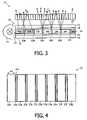
- FIG. 3is a schematic diagram of a display in a 3D imaging mode comprising a waveguide according to a second embodiment of the invention
- FIG. 4is a plan view of an array of column electrodes provided in the waveguide of the second embodiment
- FIG. 5is an exploded perspective view of a diffusing layer and electrodes in the waveguide of the second embodiment
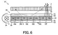
- FIG. 6is a schematic diagram of the waveguide of the second embodiment when the display of FIG. 3 is in a 2D imaging mode
- FIG. 7illustrates the light pattern produced by the waveguide of the second embodiment, when arranged to simultaneously display 2D and 3D images;
- FIG. 8is a schematic diagram of a personal digital assistant incorporating the display of FIG. 3 ;
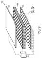
- FIG. 9is an exploded perspective view of a diffusing layer and electrodes in a waveguide according to a third embodiment of the invention.
- FIG. 10shows part of an electrode structure for use in a waveguide according to a fourth embodiment of the invention.
- FIG. 11depicts an active matrix arrangement for use with the electrode structure of FIG. 10 ;
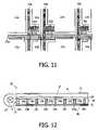
- FIG. 12is a schematic diagram of a display comprising a waveguide according to a fifth embodiment of the invention.
- FIG. 13is a schematic diagram of a display comprising a waveguide according to a sixth embodiment of the invention.
- FIG. 14is a plan view of an electrode structure used in the waveguide of FIG. 13 .
- FIG. 2depicts a display 8 , comprising a display panel 2 and an illumination system comprising a backlight 3 , such as a fluorescent rod lamp, and a waveguide 9 .
- a backlight 3such as a fluorescent rod lamp
- the display panel 2comprises a layer of electro-optically active material, such as a liquid crystal material, sandwiched between two light-transmissive substrates (not shown).
- a liquid crystal layerthe operation of the layer may be based on, for example, a twisted nematic (TN), super-twisted nematic (STN), vertically aligned nematic (VAN), optically compensated birefringence (OCB), in-plane switching nematics (IPS) or ferro-electric effect for modulating a polarisation direction of incident light.
- the display panel 2is subdivided into an array of pixels and is provided with an active matrix or a passive matrix arrangement (not shown) for driving the pixels to allow an image to be displayed in a manner well known per se.
- the waveguide 9comprises an array of portions 10 a to 10 f of a diffusing material.
- suitable diffusive materialsinclude a polymer dispersed liquid crystal (PDLC), which is diffusive in the absence of an electric field and plastics material containing particles of another material for scattering incident light, such as Polymethyl methacrylate (PMMA) containing embedded titanium oxide particles.
- PDLCpolymer dispersed liquid crystal
- PMMAPolymethyl methacrylate
- the diffusing portions 10 a to 10 fare separated by non-diffusing regions, which comprise a transparent material that is free from scattering particles.
- the diffusing portions 10 a to 10 fare sandwiched between substrates 11 , 12 .
- the substrates 11 , 12are made from a transparent material such as, for example, glass, silicon dioxide (SiO 2 ), quartz or a suitable plastic material.
- the refractive indices of the non-diffusing regions and substrates 11 , 12are substantially equal.
- An end face 13 of the waveguide 9is arranged to receive light emitted by the light source 3 either directly or, where provided, reflected by an associated reflector 14 .
- Lightpropagates through the waveguide 9 and is reflected, by total internal reflection, at the outer faces of the substrates 11 , 12 .
- light incident on a diffusing portion 10 a to 10 fis scattered in a random direction and may leave the waveguide 9 through an exit face 15 that is arranged to face the display panel 2 .
- the light that leaves the waveguide 9 through exit face 15forms a pattern of light lines that illuminate the display panel 2 . Examples of paths followed by light within the waveguide 9 are shown using dotted lines in FIG. 2 .
- each diffusing portion 10 a to 10 fcauses a column of four pixels in the display panel 2 to be illuminated.
- Each of the pixels within the columnmay present a different view, for example, views A, B, C and D, so that a viewer positioned at a suitable location may perceive a 3D image by registering an appropriate pair of views.
- the diffusing portions 10 a to 10 f in the waveguide 9 of FIG. 2produce a pattern of light lines by scattering light from the light source 3 .
- Lightmay continue to propagate through the waveguide 9 until it is scattered by a diffusing portion and exits the waveguide through one of the exit face 15 , a face 16 of the substrate 12 remote from the display panel 2 or an end face, for example, end face 13 , of the waveguide 9 .
- the light efficiency of the waveguide 9compares favourably with the prior art arrangement of FIG. 1 , in which light lines are formed by blocking and discarding unwanted light.
- the waveguide 9 of FIG. 2is configured for use in producing 3D images and cannot be used for 2D imaging.
- a switchable 2D/3D display 17is shown in FIG. 3 , which includes a waveguide 18 according to a second embodiment of the invention.
- the waveguide 18comprises diffusing portions 10 a to 10 f sandwiched between transparent substrates 11 , 12 and is arranged to guide light emitted by a light source 3 entering through an end face 13 of the waveguide 18 towards a display panel 2 in a similar manner to that discussed in relation to the first embodiment.
- the waveguide 18differs from the waveguide 9 of FIG. 2 in comprising a continuous layer 19 of switchable diffusing material.
- the diffusing materialis a liquid crystal (LC) gel and the layer has a thickness in the range of 6 to 18 ⁇ m.
- the LC gelcomprises the following components:
- the LC gelis formed by photopolymerisation of these components. Before photo-polymerisation, the blend is aligned at a surface alignment layer and is transparent. After photopolymerisation, by exposure to ultra-violet (UV) light, a polymer network micro-phase separates, comprising polymer network molecules having the same alignment and preferably the same optical properties, that is, similar ordinary and extraordinary refractive indices. This micro-phase, a so-called LC gel, is transparent.
- UVultra-violet
- the refractive index of the LC gelbecomes inhomogeneous. Multi-domains may be formed in the unphotopolymerised liquid crystal. The refractive index transitions within the LC gel, result in scattering of incident light.
- the voltage required to switch the LC gel into a diffusive stateis between 60 and 120 Volts, depending on the thickness of the layer 19 .
- the diffusing layer 19may be formed from a PDLC, which is diffusive in the absence of an electric field but becomes transparent when a voltage is applied.
- a PDLCwhich is diffusive in the absence of an electric field but becomes transparent when a voltage is applied.
- an LC gel layer 19may be less diffusive than a PDLC layer, resulting in a higher transmittance.
- the time required for an LC gel to respond to an electric fieldmay be of the order of milliseconds and compares favourably with typical PDLC materials, which may switch with rates of tens of milliseconds.
- the waveguide 18is arranged so that portions 10 a to 10 f , 19 a to 19 g of the continuous diffusive layer 19 can be switched between a transparent state and a diffusing state using a passive matrix addressing arrangement.
- the substrates 11 , 12are coated with a layer of transparent conducting material 20 , 21 , such as indium tin oxide (ITO).
- ITO layer 20 , 21is configured to form an array of electrodes, as shown in FIGS. 4 and 5 .
- a plurality of column electrodes 22 a to 22 f , 23 a to 23 gis defined in ITO layer 21 .
- a set of row electrodes, indicated generally by 24is defined in the other ITO layer 20 .
- a drive unit 25is provided for applying voltages to the electrodes 22 a to 22 f , 23 a to 23 g , 24 .
- a region 10 a to 10 f , 19 a to 19 g of the diffusive layer 19may be switched into, or maintained in, a diffusive state by applying an electric field using the appropriate column electrode 23 a to 23 f and one or more of the row electrodes 24 .
- one set of column electrodes 22 a to 22 fis configured for use in producing a pattern of light lines for 3D imaging.
- the sizes and positions of the column electrodes 22 a to 22 fare arranged to correspond to portions 10 a to 10 f of the switchable layer 19 , which are then maintained in a diffusive state.
- the diffusive portions 10 a to 10 fact on light entering the waveguide 18 in the same manner as described in relation to the first embodiment.
- the state of portions 19 a to 19 g of the diffusive layer 19located adjacent to, and between, portions 10 a to 10 f , can be controlled using electrodes 23 a to 23 g .
- the switchable portions 19 a to 19 gare light-transmissive, and light lines are produced by the waveguide 18 .
- the switchable portions 19 a to 19 gcan be switched into a diffusive state.
- all the switchable portions 19 a to 19 gare diffusive, as shown in FIG.
- uniform backlighting for the display panel 2is produced as light is scattered by all regions 10 a to 10 f , 19 a to 19 g of the diffusive layer 19 .
- the dimensions of the electrodes 22 a to 22 f and 23 a to 23 g and, therefore, the portions 10 a to 10 f , 19 a to 19 gare selected so that cross-talk between views A, B, C, D is limited to an acceptable level.
- the electrodes 23 a to 23 ghave a width w 1 of approximately 405 ⁇ m, while electrodes 22 a to 22 f have a width w 2 of approximately 50 ⁇ m.
- the dimensions used in other embodiments of the inventionwill depend on the type of display 16 and its pixel size.
- the electrodes 22 a to 22 f and 23 a to 23 gare configured to produce light lines with a width selected from a range of 10 to 800 ⁇ m with a pitch of between 100 ⁇ m to 10 mm.
- the width of the light linewill be less than, or equal to, half the pitch in order to limit cross-talk.
- the alignment of the liquid crystal within the diffusing layer 19 in the absence of an electric fieldmay be parallel or perpendicular to a propagating wave in the waveguide or perpendicular to the surface of the ITO layers 20 , 21 . If an arrangement in which the alignment is perpendicular to the ITO layers 20 , 21 is required, the LC gel must have a net negative dielectric anisotropy.
- the display 17may be used to show 2D and 3D images simultaneously.
- switchable portions 19 a , 19 b , 19 gare in a diffusive state and so, together with diffusive portions 10 a , 10 b , 10 f , produce uniform illumination, while switchable portions 19 c , 19 d , 19 e , 19 f are light-transmissive, so that light lines are produced in a limited area of the exit face 15 , by diffusive portions 10 c , 10 d and 10 e.
- FIG. 7shows a pattern of light emitted by the waveguide 18 , comprising a first area 26 of uniform illumination for one or more 2D images and a second area 27 comprising light lines for 3D images.
- the display 17may be incorporated in a device such as a PDA 28 , in a user interface that further comprises keys 29 , is used to present a 2D image 30 , such as text and/or wallpaper, and a 3D picture image 31 simultaneously.
- the 3D imagecomprises multiple views A, B.
- FIG. 5shows an arrangement in which the row electrodes 24 are provided by ITO layer 20 closest to the exit face 15 and column electrodes 22 a to 22 f , 23 a to 23 g are provided by ITO layer 21
- a waveguidecomprising this type of electrode structure can be devised in which the row electrodes 24 are provided by ITO layer 21 and the column electrodes 22 a to 22 f , 23 a to 23 g by the ITO layer 20 .
- FIG. 9shows a diffusing layer 19 and ITO layers 20 , 21 for use in a waveguide, not shown, according to a third embodiment of the invention.
- a single, unstructured, electrode 24 ais provided by the ITO layer 20 .
- a drive unit 25applies voltages to selected electrodes 22 a to 22 f , 23 a to 23 g , 24 a in order to control the optical properties of various regions 10 a to 10 f , 19 a to 19 g of the diffusive layer 19 .
- the diffusive layer 19is capable of providing illumination for 2D and 3D images simultaneously, by switching regions 19 a to 19 g accordingly.
- each region 19 a to 19 gcannot vary along the direction of the column electrodes 23 a to 23 g .
- FIG. 9shows an arrangement in which the unstructured electrode 24 a and column electrodes 22 a to 22 f , 23 a to 23 g are provided by ITO layers 20 and 21 respectively
- the electrode structuresmay be interchanged in an alternative embodiment, so that the ITO layer 20 provides the array of column electrodes 22 a to 22 f , 23 a to 23 g and ITO layer 21 constitutes the single electrode 24 a.
- the drive unit 25applies voltages to row electrodes 24 and column electrodes 22 a to 22 f , 23 a to 23 g using passive matrix addressing.
- regions 10 a to 10 f , 19 a to 19 g of the diffusive layer 19are addressed using an active matrix.
- FIG. 10depicts an ITO layer 21 provided on a substrate 12 .
- the substrate 12may be used in place of that shown in the waveguide 18 of FIG. 3 .
- the ITO layer 21is divided into pixels, forming a two-dimensional array of electrodes 22 a to 22 c , 22 p , 23 a to 23 c , 23 p to 23 s .
- the pixel electrodes 22 a to 22 c , 22 p , 23 a to 23 c , 23 p to 23 shave one of two widths w 1 , w 2 , depending on their location, in a similar manner to the column electrodes 22 a to 22 f , 23 a to 23 g of FIG. 4 .
- the substrate 12also carries an array of transistors, such as back-channel etched thin film transistors (TFTs) 32 a , 32 b , 32 c and a plurality of capacitors (not shown), where one TFT 32 a , 32 b , 32 c and one capacitor is associated with each pixel electrode 22 a , 22 b , 22 p , 22 q , 23 a , 23 b , 23 p , 23 q .
- TFTsback-channel etched thin film transistors
- TFT 32 aIn order to apply a voltage to a selected pixel electrode 23 b , TFT 32 a is activated by a voltage applied to a row electrode 33 a , causing its associated capacitor to be charged up according to the voltage on column electrode 34 b . The accumulated voltage is then supplied to a pixel electrode 23 b , in order to switch part of region 19 b of the diffusive layer 19 into a diffusive state.
- an active matrix arrangementprovides greater flexibility in allowing the creation of illumination for several 3D image windows simultaneously, so that a plurality of 3D images may be displayed simultaneously with one or more 2D images.
- a given region 19 amay be tuned to a particular scattering strength, independently of the other regions 19 b to 19 g .
- Such a featuremay be used to provide dissimilar levels of illumination to different parts of the display panel 2 simultaneously, for example, to compensate for variations in brightness and/or contrast in different parts of the display panel 2 .
- the surfaces of the waveguides 9 , 18 of the first to fourth embodimentsare not provided with reflective coatings and so, as light is scattered in random directions by diffusing portions 10 a to 10 f and, in the second embodiment, switchable portions 19 a to 19 g , a significant fraction of the light may leave the waveguide through a surface other than the exit face 15 .
- lightmay leave through face 16 of substrate 12 , or through an end face, such as end face 13 . This light cannot be recovered without causing deterioration in the contrast of the light lines.
- a fifth embodiment of the inventionwhich can achieve a higher light efficiency than the waveguides 9 , 18 of the first to fourth embodiments, while maintaining the contrast achieved by the light lines, is illustrated in FIG. 12 .
- a waveguide 35according to a fifth embodiment of the invention comprises a first substrate 11 , diffusive portions 10 a to 10 h , a diffusing layer 19 and ITO layers 20 , 21 arranged into row and column electrodes 22 a to 22 f , 23 a to 23 g , 24 as described in relation to the second embodiment.
- a light-reflective surface 36is provided in place of substrate 12 in order to recover light that is scattered by a part of the diffusing layer 19 in a direction away from the exit face 15 .
- the diffusing layer 19is situated close to the light-reflective surface 36 , a pattern of light lines with a reasonable contrast can be maintained.
- a similar configurationcan be used for a non-switchable waveguide.
- a waveguide(not shown) may be formed using a first substrate 11 , together with a reflective surface 36 as in FIG. 12 , and non-switchable diffusing portions 10 a to 10 f as discussed in relation to the first embodiment, shown in FIG. 2 .
- This configurationachieves similar advantages to those described in relation to the third embodiment.
- the 3D images produced by a display 8 , 17 comprising a waveguide 9 , 18 , 35 according to one of the first to fifth embodimentscan only be viewed from a limited number of predetermined positions, that is, a viewer must be located at a position in which the appropriate images A, B, or A, B, C, D, can be registered correctly, as shown in the prior arrangement of FIG. 1 . If the viewer should move sideways, the correct pair of images may not be perceived as the light lines and image would not be correctly aligned. The viewer may move towards, or away from, the display panel 2 . Alternatively, the direction of the viewers gaze may no longer be perpendicular to the display panel 2 .
- FIG. 13depicts a display 37 comprising a waveguide 38 according to a sixth embodiment of the invention, configured to compensate for movement of a viewer.
- the waveguide 38differs from the waveguide 18 of the second embodiment in the arrangement of column electrodes provided in ITO layer 21 .
- an array 39 of column electrodes 39 a , 39 b and so on, having substantially similar physical dimensions,is provided.
- the column electrodes 39 a , 39 bhave widths w 3 of approximately 50 ⁇ m.
- the other ITO layer 20may provide a single unstructured electrode or an array of row electrodes.
- a tracking arrangementcomprising a processor 40 and tracking devices is provided for determining the position of a viewer 6 .
- the tracking devicesare three ultrasonic transducers 41 a , 41 b , 41 c .
- the transducers 41 a , 41 b , 41 care positioned at spatial intervals in the vicinity of or, if required, within, the display 37 .
- the processor 40causes one of the ultrasonic transducers 41 b to emit an ultrasound pulse and receives output signals from the transducers 41 a , 41 c generated in response to the detection of echoes caused by reflection of the pulse by the viewer. The times at which the echoes were received and their intensity are analysed by the processor 40 in order to determine the position of the viewer 6 .
- the processor 40determines an appropriate pattern of light lines required to display a 3D image to the viewer 6 .
- the processor 40sends a control signal to the drive unit 25 , which applies voltages through selected groups of electrodes 39 a , 39 b , switching parts of the diffusive layer 19 into a diffusive state, in order to produce the required light pattern. in FIG. 13 .
- a second control signalis sent by the processor 40 to an image processor 42 .
- the image processor 42adjusts the image to be displayed in accordance with the viewer position. For example, the images displayed by each column of pixels may be manipulated in order to compensate for the viewer having an oblique view of the display panel 2 , as shown in FIG. 13 .
- Alternative sensors for detecting the position or movement of the viewer 6may be provided in place of the ultrasonic transducers 41 a , 41 b , 41 c .
- One suitable alternativeuses a single camera that monitors a viewing zone in front of the display panel 2 .
- the processor 40is equipped with software for determining the position of the viewer or his eyes from images recorded by the camera.
- a display substantially similar to that shown in FIG. 13may be provided, where the waveguide comprises an array of column electrodes, similar to the array 39 of FIG. 14 , where the widths of the column electrodes, equivalent to 39 a , 39 b etc., are less than the width of a light line, where an electric field may be applied to a diffusing layer using a plurality of adjacent column electrodes in order to provide each diffusive portion.
- a width of approximately one fifth of the width of the light lineswould be suitable, so that column electrodes with a width of 2 ⁇ m would be used in a waveguide configured to produce light lines of 10 ⁇ m width.
- column electrodes of width 160 ⁇ mcould be used in a waveguide configured to produce light lines of 800 ⁇ m width.
- Such a displaycan respond to a determination by a tracking arrangement that the viewer 6 has moved away from, or towards, the display panel by increasing or decreasing the pitch of the light lines respectively. This is achieved by applying voltages to a suitable number of column electrodes in order to switch portions of the diffusive layer into a diffusive state in order to produce light lines with the required spacing.
- the image displayed by the display panelmay also be adjusted in accordance with the detected viewer position.
- the substrates 11 , 12 , diffusing layer 19 , layers 20 , 21 and, therefore, electrodes 22 , 23 , 24 , 24 a , 33 a , 34 , 39may be provided using suitable materials other than those mentioned above.
- the electrodes 22 , 23 , 24 , 24 a , 33 a , 34 , 39may be formed using a transparent electrically conductive film of a material other than ITO, such as tin oxide (SnO 2 ).
- a waveguide according to the inventionmay be used to illuminate other types of display panel 2 , including micromechanical displays.
- the column electrodes in the waveguides of the second, third, fifth and sixth embodiments described abovemay be provided by either one of the ITO layers 20 , 21 , with a complementary electrode, that is, a single unstructured electrode 24 a or an array or row electrodes 24 being provided on the other of the ITO layers 20 , 21 .
- the active matrix described in relation to the fourth embodimentmay be provided on. substrate 11 , instead of substrate 12 .
- an active matrix arrangementmay instead be used to tune portions of a diffusing layer 19 in a similar manner discussed in relation to the electrode structure shown in FIGS. 10 and 11 .
- FIG. 8depicted a PDA 26 comprising a display and waveguide according to the invention
- the displaymay be used in other devices.
- the displaymay be incorporated in, for example, mobile telephones and other communication devices, games consoles and devices, televisions, automotive displays and displays for audio/visual or computing equipment, whether fixed or portable.
Landscapes
- Physics & Mathematics (AREA)
- Engineering & Computer Science (AREA)
- Multimedia (AREA)
- Signal Processing (AREA)
- General Physics & Mathematics (AREA)
- Optics & Photonics (AREA)
- Nonlinear Science (AREA)
- Mathematical Physics (AREA)
- Chemical & Material Sciences (AREA)
- Crystallography & Structural Chemistry (AREA)
- Liquid Crystal (AREA)
- Light Guides In General And Applications Therefor (AREA)
Abstract
Description
where pdis the pitch of the sub-pixels and a is the required parallax between each view at the position of the user. The relationship between the viewing distance d, the parallax a and the barrier-to-panel distance c is given by
- A liquid crystal blend. This may be a commercially available LC blend, for example, BL109 commercialised by Merck (RTM), and/or may have a large birefringence to enhance its scattering properties;
- A liquid crystalline monomer, such as those described in D. J. Broer et al., 1989, Makromol. Chem. 190, 3201-3215 and in D. J. Broer, “Photoinitiated polymerization and crosslinking of liquid-crystalline systems”, Radiation Curing Polym. Si. Technol. (ed. J-P. Fouassier, J. Rabek), 1993,
volume 3, 383-443. One suitable example is a liquid crystalline diacrylate with the following chemical structure, at a concentration of between 6 and 12 Wt %:

- a photoinitiator, for example, Irgacure 651, manufactured by Ciba Geigy®. The amount is normally about 1% calculated on the amount of reactive monomer.
Claims (23)
Applications Claiming Priority (3)
| Application Number | Priority Date | Filing Date | Title |
|---|---|---|---|
| GBGB0326005.6AGB0326005D0 (en) | 2003-11-07 | 2003-11-07 | Waveguide for autostereoscopic display |
| GB0326005.6 | 2003-11-07 | ||
| PCT/IB2004/052287WO2005045488A1 (en) | 2003-11-07 | 2004-11-03 | Waveguide for autostereoscopic display |
Publications (2)
| Publication Number | Publication Date |
|---|---|
| US20070091638A1 US20070091638A1 (en) | 2007-04-26 |
| US7626643B2true US7626643B2 (en) | 2009-12-01 |
Family
ID=29726122
Family Applications (1)
| Application Number | Title | Priority Date | Filing Date |
|---|---|---|---|
| US10/578,071Expired - LifetimeUS7626643B2 (en) | 2003-11-07 | 2004-11-03 | Waveguide for autostereoscopic display having a plurality of switchable portions of diffusive material within the waveguide for providing either scattering or light-transmissive light to the display |
Country Status (8)
| Country | Link |
|---|---|
| US (1) | US7626643B2 (en) |
| EP (1) | EP1682932B1 (en) |
| JP (1) | JP4917892B2 (en) |
| KR (1) | KR20060114694A (en) |
| CN (1) | CN100504465C (en) |
| GB (1) | GB0326005D0 (en) |
| TW (1) | TW200522720A (en) |
| WO (1) | WO2005045488A1 (en) |
Cited By (28)
| Publication number | Priority date | Publication date | Assignee | Title |
|---|---|---|---|---|
| US20070216828A1 (en)* | 2004-01-17 | 2007-09-20 | Jacobs Adrian M | Display |
| US20080163663A1 (en)* | 2007-01-05 | 2008-07-10 | Apple Inc | Compact tube with internal features and methods for fabricating the same |
| US20080166005A1 (en)* | 2007-01-05 | 2008-07-10 | Apple Inc | Headset electronics |
| US20080164934A1 (en)* | 2007-01-06 | 2008-07-10 | Apple Inc. | Connectors designed for ease of use |
| US20080252720A1 (en)* | 2007-04-12 | 2008-10-16 | Samsung Electronics Co., Ltd. | Highly efficient 2d-3d switchable display device |
| US20080291364A1 (en)* | 2007-05-18 | 2008-11-27 | Dong-Gun Moon | Light emission device and display device using the light emission device as a light source |
| US20100026797A1 (en)* | 2007-01-03 | 2010-02-04 | Koninklijke Philips Electronics, N.V. | Display device |
| US20100079843A1 (en)* | 2008-08-22 | 2010-04-01 | Derichs Kevin J | Normally emitting pixel architecture for frustrated total internal reflection displays |
| US7982823B1 (en) | 2010-06-17 | 2011-07-19 | Sharp Laboratories Of America, Inc. | Area active backlight with steerable backlight |
| US20120162762A1 (en)* | 2010-12-28 | 2012-06-28 | Sony Corporation | Stereoscopic display unit and barrier device |
| US20120194509A1 (en)* | 2011-01-31 | 2012-08-02 | Samsung Electronics Co., Ltd. | Method and apparatus for displaying partial 3d image in 2d image display area |
| US20130082921A1 (en)* | 2011-09-30 | 2013-04-04 | Soon Seok Kang | Barrier panel, and 3d image display device and method using the same |
| US8870380B2 (en) | 2012-09-11 | 2014-10-28 | Delta Electronics, Inc. | System and method for time-multiplexed autostereoscopic display |
| US9052421B2 (en) | 2012-10-15 | 2015-06-09 | Samsung Display Co., Ltd. | Backlight unit for display device and driving method thereof |
| US9128226B2 (en) | 2013-07-30 | 2015-09-08 | Leia Inc. | Multibeam diffraction grating-based backlighting |
| US9294830B2 (en) | 2005-09-26 | 2016-03-22 | Apple Inc. | Wireless headset having adaptive powering |
| US9298168B2 (en) | 2013-01-31 | 2016-03-29 | Leia Inc. | Multiview 3D wrist watch |
| US9389415B2 (en) | 2012-04-27 | 2016-07-12 | Leia Inc. | Directional pixel for use in a display screen |
| US9459461B2 (en) | 2012-05-31 | 2016-10-04 | Leia Inc. | Directional backlight |
| US9507197B2 (en) | 2010-04-06 | 2016-11-29 | Sony Corporation | Lighting device and display device |
| US9557466B2 (en) | 2014-07-30 | 2017-01-31 | Leia, Inc | Multibeam diffraction grating-based color backlighting |
| US9837009B2 (en) | 2013-12-09 | 2017-12-05 | Samsung Electronics Co., Ltd. | Apparatus and method for driving display panel |
| US9967646B2 (en) | 2007-01-06 | 2018-05-08 | Apple Inc. | Headset connector |
| US20190025494A1 (en)* | 2016-01-30 | 2019-01-24 | Leia Inc. | Multibeam element-based backlight and display using same |
| US10397557B2 (en) | 2015-03-26 | 2019-08-27 | Koninklijke Philips N.V. | Display device with directional control of the output, and a backlight for such a display device and a light direction method |
| US10582284B2 (en) | 2015-09-30 | 2020-03-03 | Apple Inc. | In-ear headphone |
| US10798371B2 (en) | 2015-09-05 | 2020-10-06 | Leia Inc. | Multiview display with head tracking |
| US12177414B2 (en) | 2018-08-26 | 2024-12-24 | Leia Inc. | Multiview display, system, and method with user tracking |
Families Citing this family (79)
| Publication number | Priority date | Publication date | Assignee | Title |
|---|---|---|---|---|
| ATE527705T1 (en)* | 2004-12-06 | 2011-10-15 | Koninkl Philips Electronics Nv | ORGANIC ELECTROLUMINescent LIGHT SOURCE |
| GB2426351A (en) | 2005-05-19 | 2006-11-22 | Sharp Kk | A dual view display |
| GB2428129A (en)* | 2005-07-08 | 2007-01-17 | Sharp Kk | A multiple-view directional display |
| KR101167318B1 (en)* | 2005-08-31 | 2012-07-19 | 엘지디스플레이 주식회사 | stereoscopic image display device |
| KR20070077415A (en)* | 2006-01-23 | 2007-07-26 | (주)쓰리디아이에스 | Stereoscopic video display |
| DE102006013407A1 (en)* | 2006-03-20 | 2007-09-27 | Newsight Gmbh | Arrangement for optionally three-dimensionally perceptible or two-dimensional representation of images |
| EP1943555B1 (en)* | 2006-10-06 | 2012-05-02 | QUALCOMM MEMS Technologies, Inc. | Optical loss structure integrated in an illumination apparatus of a display |
| RU2326507C1 (en)* | 2006-12-12 | 2008-06-10 | Евгений Борисович Гаскевич | Stereo image generation system |
| KR101439842B1 (en)* | 2007-06-25 | 2014-09-12 | 삼성전자주식회사 | Backlight unit and 2D-3D switchable image display apparatus employing the same |
| TW200925023A (en)* | 2007-12-07 | 2009-06-16 | Altek Corp | Method of displaying shot image on car reverse video system |
| GB2457691A (en)* | 2008-02-21 | 2009-08-26 | Sharp Kk | Display with regions simultaneously operable in different viewing modes |
| US20110050127A1 (en)* | 2008-05-08 | 2011-03-03 | Koninklijke Philips Electronics N.V. | Lighting device |
| KR100961903B1 (en)* | 2008-06-09 | 2010-06-10 | 주식회사 토비스 | Backlight unit, and liquid crystal display and game machine including the same |
| RU2473941C2 (en)* | 2008-09-25 | 2013-01-27 | Шарп Кабусики Кайся | Light flux control device, lit-up unit, lc display panel, and lc display |
| KR101658793B1 (en) | 2008-10-09 | 2016-09-23 | 삼성전자주식회사 | Apparatus and method for 2d and 3d image switchable display |
| JP2010157475A (en)* | 2009-01-05 | 2010-07-15 | Sony Corp | Illuminating device and display device |
| EP2401639B1 (en)* | 2009-02-24 | 2019-09-18 | AGC Glass Europe | Laminated glass diffused lighting panel and method of manufacturing it |
| TWI419124B (en) | 2009-03-06 | 2013-12-11 | Au Optronics Corp | 2d/3d image displaying apparatus |
| JP2010237416A (en)* | 2009-03-31 | 2010-10-21 | Sharp Corp | 3D display device |
| DE102009003069A1 (en)* | 2009-05-13 | 2010-11-25 | Seereal Technologies S.A. | 3D display with controllable visibility tracker |
| KR101652471B1 (en) | 2009-06-16 | 2016-08-30 | 삼성전자주식회사 | Display device and method thereof |
| US20110242298A1 (en)* | 2009-08-21 | 2011-10-06 | Microsoft Corporation | Private video presentation |
| US9247286B2 (en) | 2009-12-31 | 2016-01-26 | Broadcom Corporation | Frame formatting supporting mixed two and three dimensional video data communication |
| US8823782B2 (en) | 2009-12-31 | 2014-09-02 | Broadcom Corporation | Remote control with integrated position, viewer identification and optical and audio test |
| US8854531B2 (en) | 2009-12-31 | 2014-10-07 | Broadcom Corporation | Multiple remote controllers that each simultaneously controls a different visual presentation of a 2D/3D display |
| US20110157322A1 (en) | 2009-12-31 | 2011-06-30 | Broadcom Corporation | Controlling a pixel array to support an adaptable light manipulator |
| WO2011113180A1 (en) | 2010-03-19 | 2011-09-22 | Nokia Corporation | Apparatus, methods and computer programs for configuring output of a display |
| JP2011222237A (en)* | 2010-04-07 | 2011-11-04 | Sony Corp | Lighting system and display device |
| JP4930631B2 (en)* | 2010-09-27 | 2012-05-16 | ソニー株式会社 | 3D display device |
| KR101729023B1 (en)* | 2010-10-05 | 2017-04-21 | 엘지전자 주식회사 | Mobile terminal and operation control method thereof |
| US9201185B2 (en) | 2011-02-04 | 2015-12-01 | Microsoft Technology Licensing, Llc | Directional backlighting for display panels |
| TWI569041B (en) | 2011-02-14 | 2017-02-01 | 半導體能源研究所股份有限公司 | Display device |
| US9443455B2 (en)* | 2011-02-25 | 2016-09-13 | Semiconductor Energy Laboratory Co., Ltd. | Display device having a plurality of pixels |
| JP2012226199A (en)* | 2011-04-21 | 2012-11-15 | Sony Corp | Light source device and display |
| JP5699786B2 (en)* | 2011-04-28 | 2015-04-15 | ソニー株式会社 | Display device and lighting device |
| JP5948813B2 (en) | 2011-05-09 | 2016-07-06 | ソニー株式会社 | Illumination device and display device |
| JP2012252993A (en) | 2011-05-10 | 2012-12-20 | Sony Corp | Lighting device and display device |
| CN102316341B (en)* | 2011-05-16 | 2014-03-12 | 深圳超多维光电子有限公司 | 2D-3D display mode switching method and corresponding display equipment |
| JP5685154B2 (en)* | 2011-06-21 | 2015-03-18 | 株式会社ジャパンディスプレイ | Stereoscopic image display device and driving method of stereoscopic image display device |
| JP2013050694A (en) | 2011-07-29 | 2013-03-14 | Sony Corp | Illumination device and display device |
| JP2013054331A (en)* | 2011-08-05 | 2013-03-21 | Sony Corp | Display method, display device, electronic system, and lighting unit |
| JP5991053B2 (en)* | 2011-10-04 | 2016-09-14 | ソニー株式会社 | Display device and lighting device |
| JP5906649B2 (en)* | 2011-10-05 | 2016-04-20 | ソニー株式会社 | Display device |
| CN102395039B (en)* | 2011-11-18 | 2013-09-11 | 南开大学 | Follow-up illuminating free stereo video image display |
| TW201326982A (en)* | 2011-12-29 | 2013-07-01 | Ind Tech Res Inst | Display apparatus |
| US9354748B2 (en) | 2012-02-13 | 2016-05-31 | Microsoft Technology Licensing, Llc | Optical stylus interaction |
| US9075566B2 (en) | 2012-03-02 | 2015-07-07 | Microsoft Technoogy Licensing, LLC | Flexible hinge spine |
| US9460029B2 (en) | 2012-03-02 | 2016-10-04 | Microsoft Technology Licensing, Llc | Pressure sensitive keys |
| US9870066B2 (en) | 2012-03-02 | 2018-01-16 | Microsoft Technology Licensing, Llc | Method of manufacturing an input device |
| US20130300590A1 (en) | 2012-05-14 | 2013-11-14 | Paul Henry Dietz | Audio Feedback |
| US9256089B2 (en) | 2012-06-15 | 2016-02-09 | Microsoft Technology Licensing, Llc | Object-detecting backlight unit |
| US20140022241A1 (en)* | 2012-07-18 | 2014-01-23 | Electronics And Telecommunications Research Institute | Display apparatus and method based on symmetrically spb |
| JP6098064B2 (en)* | 2012-08-08 | 2017-03-22 | ソニー株式会社 | Display device and lighting device |
| WO2014051623A1 (en)* | 2012-09-28 | 2014-04-03 | Hewlett-Packard Development Company, L. P. | Directional waveguide-based backlight for use in a multivew display screen |
| JP5954097B2 (en)* | 2012-10-11 | 2016-07-20 | ソニー株式会社 | Display device |
| US9552777B2 (en) | 2013-05-10 | 2017-01-24 | Microsoft Technology Licensing, Llc | Phase control backlight |
| TWI495904B (en)* | 2013-07-12 | 2015-08-11 | Vision Technology Co Ltd C | Field sequential color lcd and method for generating 3d images by matching a software optical grating |
| CN104423054B (en)* | 2013-08-30 | 2017-01-11 | 张家港康得新光电材料有限公司 | Method and device capable of simultaneously displaying 2D (two-dimensional) image and 3D image |
| EP3936934B1 (en)* | 2014-03-21 | 2024-04-24 | RealD Spark, LLC | Directional backlight |
| KR20150122341A (en)* | 2014-04-23 | 2015-11-02 | 삼성전자주식회사 | Back light apparatus and 3d display apparatus including the same |
| CN104023223B (en)* | 2014-05-29 | 2016-03-02 | 京东方科技集团股份有限公司 | Display control method, Apparatus and system |
| CN106461997A (en)* | 2014-05-30 | 2017-02-22 | 3M创新有限公司 | Variable viewing angle optical systems |
| KR20160059783A (en) | 2014-11-19 | 2016-05-27 | 삼성전자주식회사 | Back light unit, display device comprising the same and method for manufacturing the same |
| KR102367515B1 (en)* | 2014-11-19 | 2022-02-25 | 삼성전자주식회사 | Back light unit, display device comprising the same and method for manufacturing the same |
| JP6567058B2 (en)* | 2015-01-10 | 2019-08-28 | レイア、インコーポレイテッドLeia Inc. | 2D / 3D (2D / 3D) switchable display backlight and electronic display |
| US10591869B2 (en)* | 2015-03-24 | 2020-03-17 | Light Field Lab, Inc. | Tileable, coplanar, flat-panel 3-D display with tactile and audio interfaces |
| JP7073249B2 (en)* | 2015-07-16 | 2022-05-23 | メルク パテント ゲゼルシャフト ミット ベシュレンクテル ハフツング | A device for controlling the transmission of light |
| CN105304677B (en)* | 2015-09-24 | 2019-09-06 | 京东方科技集团股份有限公司 | A kind of OLED display panel and display device, display system |
| KR20230131497A (en) | 2016-07-15 | 2023-09-13 | 라이트 필드 랩 인코포레이티드 | Energy Propagation and Transverse Anderson Localization with Two-Dimensional, Light Field and Holographic Relays |
| FR3054899B1 (en)* | 2016-08-03 | 2018-08-17 | Valeo Comfort And Driving Assistance | IMAGE GENERATING DEVICE FOR SCREEN AND HEAD-UP DISPLAY |
| CN107845583B (en)* | 2016-09-18 | 2020-12-18 | 中芯国际集成电路制造(上海)有限公司 | Substrate surface defect detection device, image distortion correction method and device, and substrate surface defect detection apparatus |
| KR102667702B1 (en)* | 2016-12-06 | 2024-05-22 | 삼성전자주식회사 | Back light apparatus, display apparatus having the back light apparatus and control method for the display apparatus |
| CN107394062B (en)* | 2017-07-20 | 2019-02-05 | 京东方科技集团股份有限公司 | An organic light emitting diode display panel, a method for making the same, and a display device |
| CN112105976B (en) | 2018-01-14 | 2022-12-09 | 光场实验室公司 | Energy Field 3D Printing System |
| CN112105975A (en) | 2018-01-14 | 2020-12-18 | 光场实验室公司 | System and method for lateral energy localization using ordered structures in energy repeaters |
| JP6867320B2 (en)* | 2018-02-28 | 2021-04-28 | 浜松ホトニクス株式会社 | Light measuring device and light measuring method |
| EP4029014A4 (en)* | 2019-09-13 | 2023-03-29 | Light Field Lab, Inc. | LIGHT FIELD DISPLAY SYSTEM FOR ADULT APPLICATIONS |
| JP7483015B2 (en)* | 2020-01-20 | 2024-05-14 | レイア、インコーポレイテッド | Multi-user multi-view display, system and method thereof |
| DE102020121647A1 (en)* | 2020-08-18 | 2022-02-24 | Bayerische Motoren Werke Aktiengesellschaft | Waveguide display arrangement for a 3D head-up display device in a vehicle and method for its operation |
Citations (6)
| Publication number | Priority date | Publication date | Assignee | Title |
|---|---|---|---|---|
| US5099343A (en)* | 1989-05-25 | 1992-03-24 | Hughes Aircraft Company | Edge-illuminated liquid crystal display devices |
| US6222598B1 (en)* | 1995-11-22 | 2001-04-24 | Hitachi, Ltd. | Liquid crystal display |
| US20020018158A1 (en)* | 1999-12-23 | 2002-02-14 | Putilin Andrey N. | System and method for the manufacture of a universal reflective-transmissive display |
| US6437915B2 (en)* | 1996-09-12 | 2002-08-20 | Sharp Kabushiki Kaisha | Parallax barrier, display, passive polarization modulating optical element and method of making such an element |
| US20030067563A1 (en)* | 2001-09-11 | 2003-04-10 | Samsung Electronics Co., Ltd. | 2D/3D convertible display |
| US6618104B1 (en)* | 1998-07-28 | 2003-09-09 | Nippon Telegraph And Telephone Corporation | Optical device having reverse mode holographic PDLC and front light guide |
Family Cites Families (13)
| Publication number | Priority date | Publication date | Assignee | Title |
|---|---|---|---|---|
| GB2139392B (en)* | 1983-05-05 | 1986-10-22 | Standard Telephones Cables Ltd | Display device |
| FR2705484B1 (en)* | 1993-05-18 | 1995-06-23 | Thomson Csf | Display device. |
| JP3246701B2 (en)* | 1994-12-28 | 2002-01-15 | 日本電信電話株式会社 | 3D display device |
| JP2930185B2 (en)* | 1995-02-24 | 1999-08-03 | 松下電器産業株式会社 | Display device |
| US5897184A (en) | 1996-07-02 | 1999-04-27 | Dimension Technologies, Inc. | Reduced-thickness backlighter for autostereoscopic display and display using the backlighter |
| GB2317710A (en)* | 1996-09-27 | 1998-04-01 | Sharp Kk | Spatial light modulator and directional display |
| JPH10206848A (en)* | 1997-01-27 | 1998-08-07 | Seiko Epson Corp | Liquid crystal display device and electronic device using the same |
| JPH11237631A (en)* | 1998-02-23 | 1999-08-31 | Sanyo Electric Co Ltd | Color display device |
| JP2000075243A (en)* | 1998-08-31 | 2000-03-14 | Citizen Watch Co Ltd | Stereoscopic display device |
| US6276138B1 (en) | 1999-09-10 | 2001-08-21 | Ford Global Technologies, Inc. | Engine with direct turbo compounding |
| JP2002084553A (en)* | 2000-09-11 | 2002-03-22 | Canon Inc | 3D display device |
| DE60238691D1 (en)* | 2001-08-21 | 2011-02-03 | Koninkl Philips Electronics Nv | AUTOSTEREOSCOPIC IMAGE DISPLAY DEVICE WITH USER SUCCESSION SYSTEM |
| US6966684B2 (en)* | 2001-09-13 | 2005-11-22 | Gelcore, Llc | Optical wave guide |
- 2003
- 2003-11-07GBGBGB0326005.6Apatent/GB0326005D0/ennot_activeCeased
- 2004
- 2004-11-03USUS10/578,071patent/US7626643B2/ennot_activeExpired - Lifetime
- 2004-11-03JPJP2006537544Apatent/JP4917892B2/ennot_activeExpired - Lifetime
- 2004-11-03KRKR1020067008547Apatent/KR20060114694A/ennot_activeWithdrawn
- 2004-11-03CNCNB2004800324965Apatent/CN100504465C/ennot_activeExpired - Lifetime
- 2004-11-03WOPCT/IB2004/052287patent/WO2005045488A1/enactiveApplication Filing
- 2004-11-03EPEP04799054Apatent/EP1682932B1/ennot_activeExpired - Lifetime
- 2004-11-04TWTW093133657Apatent/TW200522720A/enunknown
Patent Citations (6)
| Publication number | Priority date | Publication date | Assignee | Title |
|---|---|---|---|---|
| US5099343A (en)* | 1989-05-25 | 1992-03-24 | Hughes Aircraft Company | Edge-illuminated liquid crystal display devices |
| US6222598B1 (en)* | 1995-11-22 | 2001-04-24 | Hitachi, Ltd. | Liquid crystal display |
| US6437915B2 (en)* | 1996-09-12 | 2002-08-20 | Sharp Kabushiki Kaisha | Parallax barrier, display, passive polarization modulating optical element and method of making such an element |
| US6618104B1 (en)* | 1998-07-28 | 2003-09-09 | Nippon Telegraph And Telephone Corporation | Optical device having reverse mode holographic PDLC and front light guide |
| US20020018158A1 (en)* | 1999-12-23 | 2002-02-14 | Putilin Andrey N. | System and method for the manufacture of a universal reflective-transmissive display |
| US20030067563A1 (en)* | 2001-09-11 | 2003-04-10 | Samsung Electronics Co., Ltd. | 2D/3D convertible display |
Cited By (60)
| Publication number | Priority date | Publication date | Assignee | Title |
|---|---|---|---|---|
| US20070216828A1 (en)* | 2004-01-17 | 2007-09-20 | Jacobs Adrian M | Display |
| US7903183B2 (en)* | 2004-01-17 | 2011-03-08 | Sharp Kabushiki Kaisha | Display including backlight operable in 2D and 3D modes |
| US9854343B2 (en) | 2005-09-26 | 2017-12-26 | Apple Inc. | Headset connector |
| US9294830B2 (en) | 2005-09-26 | 2016-03-22 | Apple Inc. | Wireless headset having adaptive powering |
| US9287657B2 (en) | 2005-09-26 | 2016-03-15 | Apple Inc. | Headset connector |
| US20100026797A1 (en)* | 2007-01-03 | 2010-02-04 | Koninklijke Philips Electronics, N.V. | Display device |
| US20080163663A1 (en)* | 2007-01-05 | 2008-07-10 | Apple Inc | Compact tube with internal features and methods for fabricating the same |
| US20080166005A1 (en)* | 2007-01-05 | 2008-07-10 | Apple Inc | Headset electronics |
| US8867758B2 (en) | 2007-01-05 | 2014-10-21 | Apple Inc. | Headset electronics |
| US8712071B2 (en) | 2007-01-05 | 2014-04-29 | Apple Inc. | Headset electronics |
| US8650925B2 (en) | 2007-01-05 | 2014-02-18 | Apple Inc. | Extrusion method for fabricating a compact tube with internal features |
| US11877112B2 (en) | 2007-01-06 | 2024-01-16 | Apple Inc. | In-ear wireless device |
| US12231837B2 (en) | 2007-01-06 | 2025-02-18 | Apple Inc. | In-ear wireless device |
| US20180255389A1 (en) | 2007-01-06 | 2018-09-06 | Apple Inc. | Headset connector |
| US10993011B2 (en) | 2007-01-06 | 2021-04-27 | Apple Inc. | In-ear wireless listening device |
| US10771880B1 (en) | 2007-01-06 | 2020-09-08 | Apple Inc. | In-ear wireless device |
| US10959006B2 (en) | 2007-01-06 | 2021-03-23 | Apple Inc. | In-ear wireless listening device |
| US10433043B2 (en) | 2007-01-06 | 2019-10-01 | Apple Inc. | In-ear listening device |
| US10165346B2 (en) | 2007-01-06 | 2018-12-25 | Apple Inc. | Headset connector |
| US10516931B2 (en) | 2007-01-06 | 2019-12-24 | Apple Inc. | Headset connector |
| US9967646B2 (en) | 2007-01-06 | 2018-05-08 | Apple Inc. | Headset connector |
| US10313775B2 (en) | 2007-01-06 | 2019-06-04 | Apple Inc. | Portable listening device system |
| US9118990B2 (en) | 2007-01-06 | 2015-08-25 | Apple Inc. | Connectors designed for ease of use |
| US11336985B2 (en) | 2007-01-06 | 2022-05-17 | Apple Inc. | In-ear wireless device |
| US10979796B2 (en) | 2007-01-06 | 2021-04-13 | Apple Inc. | In-ear wireless listening device |
| US20080164934A1 (en)* | 2007-01-06 | 2008-07-10 | Apple Inc. | Connectors designed for ease of use |
| US20080252720A1 (en)* | 2007-04-12 | 2008-10-16 | Samsung Electronics Co., Ltd. | Highly efficient 2d-3d switchable display device |
| US8319828B2 (en)* | 2007-04-12 | 2012-11-27 | Samsung Electronics Co., Ltd. | Highly efficient 2D-3D switchable display device |
| US8154684B2 (en)* | 2007-05-18 | 2012-04-10 | Samsung Sdi Co., Ltd. | Light emission device and display device using the light emission device as a light source |
| US20080291364A1 (en)* | 2007-05-18 | 2008-11-27 | Dong-Gun Moon | Light emission device and display device using the light emission device as a light source |
| US8320036B2 (en)* | 2008-08-22 | 2012-11-27 | Rambus Inc. | Normally emitting pixel architecture for frustrated total internal reflection displays |
| US20100079843A1 (en)* | 2008-08-22 | 2010-04-01 | Derichs Kevin J | Normally emitting pixel architecture for frustrated total internal reflection displays |
| US9507197B2 (en) | 2010-04-06 | 2016-11-29 | Sony Corporation | Lighting device and display device |
| US7982823B1 (en) | 2010-06-17 | 2011-07-19 | Sharp Laboratories Of America, Inc. | Area active backlight with steerable backlight |
| CN102566066A (en)* | 2010-12-28 | 2012-07-11 | 索尼公司 | Stereoscopic display unit and barrier device |
| US20120162762A1 (en)* | 2010-12-28 | 2012-06-28 | Sony Corporation | Stereoscopic display unit and barrier device |
| US9253479B2 (en)* | 2011-01-31 | 2016-02-02 | Samsung Display Co., Ltd. | Method and apparatus for displaying partial 3D image in 2D image display area |
| US20120194509A1 (en)* | 2011-01-31 | 2012-08-02 | Samsung Electronics Co., Ltd. | Method and apparatus for displaying partial 3d image in 2d image display area |
| US20130082921A1 (en)* | 2011-09-30 | 2013-04-04 | Soon Seok Kang | Barrier panel, and 3d image display device and method using the same |
| US9389415B2 (en) | 2012-04-27 | 2016-07-12 | Leia Inc. | Directional pixel for use in a display screen |
| US9459461B2 (en) | 2012-05-31 | 2016-10-04 | Leia Inc. | Directional backlight |
| US8870380B2 (en) | 2012-09-11 | 2014-10-28 | Delta Electronics, Inc. | System and method for time-multiplexed autostereoscopic display |
| US9052421B2 (en) | 2012-10-15 | 2015-06-09 | Samsung Display Co., Ltd. | Backlight unit for display device and driving method thereof |
| US9298168B2 (en) | 2013-01-31 | 2016-03-29 | Leia Inc. | Multiview 3D wrist watch |
| US9785119B2 (en) | 2013-01-31 | 2017-10-10 | Leia Inc. | Multiview display screen and multiview mobile device using same |
| US9128226B2 (en) | 2013-07-30 | 2015-09-08 | Leia Inc. | Multibeam diffraction grating-based backlighting |
| US9837009B2 (en) | 2013-12-09 | 2017-12-05 | Samsung Electronics Co., Ltd. | Apparatus and method for driving display panel |
| US9557466B2 (en) | 2014-07-30 | 2017-01-31 | Leia, Inc | Multibeam diffraction grating-based color backlighting |
| US10345505B2 (en) | 2014-07-30 | 2019-07-09 | Leia, Inc. | Multibeam diffraction grating-based color backlighting |
| US10397557B2 (en) | 2015-03-26 | 2019-08-27 | Koninklijke Philips N.V. | Display device with directional control of the output, and a backlight for such a display device and a light direction method |
| US10798371B2 (en) | 2015-09-05 | 2020-10-06 | Leia Inc. | Multiview display with head tracking |
| US11265638B2 (en) | 2015-09-30 | 2022-03-01 | Apple Inc. | In-ear headphone |
| US10841683B2 (en) | 2015-09-30 | 2020-11-17 | Apple Inc. | In-ear headphone |
| US10694276B2 (en) | 2015-09-30 | 2020-06-23 | Apple Inc. | In-ear headphone |
| US10582284B2 (en) | 2015-09-30 | 2020-03-03 | Apple Inc. | In-ear headphone |
| US11930313B2 (en) | 2015-09-30 | 2024-03-12 | Apple Inc. | In-ear headphone |
| US12284475B2 (en) | 2015-09-30 | 2025-04-22 | Apple Inc. | In-ear headphone |
| US10649128B2 (en)* | 2016-01-30 | 2020-05-12 | Leia Inc. | Multibeam element-based backlight and display using same |
| US20190025494A1 (en)* | 2016-01-30 | 2019-01-24 | Leia Inc. | Multibeam element-based backlight and display using same |
| US12177414B2 (en) | 2018-08-26 | 2024-12-24 | Leia Inc. | Multiview display, system, and method with user tracking |
Also Published As
| Publication number | Publication date |
|---|---|
| JP4917892B2 (en) | 2012-04-18 |
| GB0326005D0 (en) | 2003-12-10 |
| KR20060114694A (en) | 2006-11-07 |
| TW200522720A (en) | 2005-07-01 |
| US20070091638A1 (en) | 2007-04-26 |
| CN100504465C (en) | 2009-06-24 |
| WO2005045488A1 (en) | 2005-05-19 |
| CN1875302A (en) | 2006-12-06 |
| EP1682932B1 (en) | 2013-01-09 |
| EP1682932A1 (en) | 2006-07-26 |
| JP2007514273A (en) | 2007-05-31 |
Similar Documents
| Publication | Publication Date | Title |
|---|---|---|
| US7626643B2 (en) | Waveguide for autostereoscopic display having a plurality of switchable portions of diffusive material within the waveguide for providing either scattering or light-transmissive light to the display | |
| JP4813366B2 (en) | 2D / 3D image display | |
| KR100686293B1 (en) | Optical element and display device using same | |
| JP5991053B2 (en) | Display device and lighting device | |
| US9257063B2 (en) | Display unit | |
| US11314117B2 (en) | Display assembly, display device and control method thereof | |
| CN102096237B (en) | Transparent display device | |
| JP5929083B2 (en) | Display device | |
| US8599322B2 (en) | 2-dimensional and 3-dimensional image display device and method of manufacturing the same | |
| KR101243790B1 (en) | Three-dimensional Image Display | |
| JP2012063704A (en) | Display device | |
| KR100765308B1 (en) | Liquid crystal display | |
| US20150268478A1 (en) | Display device | |
| US20200284965A1 (en) | Light source module and display device using the same | |
| KR20170087221A (en) | Display apparatus | |
| KR101738002B1 (en) | Liquid crystal display | |
| CN115561939A (en) | Liquid crystal display device having a plurality of pixel electrodes | |
| JP2007047206A (en) | Optical sheet, electric field-controlled panel, illumination device, liquid crystal display device and method for manufacturing optical sheet | |
| JP2006119291A (en) | Liquid crystal display | |
| JP2007047205A (en) | Optical sheet, electric field-controlled panel, illumination device, liquid crystal display device and method for manufacturing optical sheet |
Legal Events
| Date | Code | Title | Description |
|---|---|---|---|
| AS | Assignment | Owner name:KONINKLIJKE PHILIPS ELECTRONICS, N.V., NETHERLANDS Free format text:ASSIGNMENT OF ASSIGNORS INTEREST;ASSIGNORS:IJZERMAN, WILLEM L.;JAK, MARTIN J.J.;REEL/FRAME:017843/0313 Effective date:20060313 | |
| STCF | Information on status: patent grant | Free format text:PATENTED CASE | |
| FPAY | Fee payment | Year of fee payment:4 | |
| FPAY | Fee payment | Year of fee payment:8 | |
| MAFP | Maintenance fee payment | Free format text:PAYMENT OF MAINTENANCE FEE, 12TH YEAR, LARGE ENTITY (ORIGINAL EVENT CODE: M1553); ENTITY STATUS OF PATENT OWNER: LARGE ENTITY Year of fee payment:12 | |
| AS | Assignment | Owner name:LEIA INC., CALIFORNIA Free format text:ASSIGNMENT OF ASSIGNORS INTEREST;ASSIGNOR:KONINKLIJKE PHILIPS N.V.;REEL/FRAME:065385/0825 Effective date:20231024 | |
| AS | Assignment | Owner name:KONINKLIJKE PHILIPS NV., NETHERLANDS Free format text:CHANGE OF NAME;ASSIGNOR:KONINKLIJKE PHILIPS ELECTRONICS N.Y.;REEL/FRAME:065598/0589 Effective date:20130515 | |
| AS | Assignment | Owner name:LELIS, INC., AS AGENT, PANAMA Free format text:SECURITY INTEREST;ASSIGNORS:LEIA, INC.;LEIA SPV LLC;DIMENCO HOLDING B.V.;REEL/FRAME:069296/0265 Effective date:20240930 |