US7623335B2 - Hermetic feedthrough terminal assembly with wire bond pads for human implant applications - Google Patents
Hermetic feedthrough terminal assembly with wire bond pads for human implant applicationsDownload PDFInfo
- Publication number
- US7623335B2 US7623335B2US11/308,662US30866206AUS7623335B2US 7623335 B2US7623335 B2US 7623335B2US 30866206 AUS30866206 AUS 30866206AUS 7623335 B2US7623335 B2US 7623335B2
- Authority
- US
- United States
- Prior art keywords
- assembly
- wire bond
- bond pad
- terminal pin
- conductive
- Prior art date
- Legal status (The legal status is an assumption and is not a legal conclusion. Google has not performed a legal analysis and makes no representation as to the accuracy of the status listed.)
- Expired - Lifetime, expires
Links
Images


Classifications
- A—HUMAN NECESSITIES
- A61—MEDICAL OR VETERINARY SCIENCE; HYGIENE
- A61N—ELECTROTHERAPY; MAGNETOTHERAPY; RADIATION THERAPY; ULTRASOUND THERAPY
- A61N1/00—Electrotherapy; Circuits therefor
- A61N1/18—Applying electric currents by contact electrodes
- A61N1/32—Applying electric currents by contact electrodes alternating or intermittent currents
- A61N1/36—Applying electric currents by contact electrodes alternating or intermittent currents for stimulation
- A61N1/372—Arrangements in connection with the implantation of stimulators
- A61N1/375—Constructional arrangements, e.g. casings
- A61N1/3752—Details of casing-lead connections
- A61N1/3754—Feedthroughs
- H—ELECTRICITY
- H01—ELECTRIC ELEMENTS
- H01G—CAPACITORS; CAPACITORS, RECTIFIERS, DETECTORS, SWITCHING DEVICES, LIGHT-SENSITIVE OR TEMPERATURE-SENSITIVE DEVICES OF THE ELECTROLYTIC TYPE
- H01G4/00—Fixed capacitors; Processes of their manufacture
- H01G4/35—Feed-through capacitors or anti-noise capacitors
Definitions
- This inventionrelates generally to hermetic feedthrough terminal subassemblies and related methods of construction, particularly of the type used in active implantable medical devices such as cardiac pacemakers, implantable defibrillators, cochlear implants, neurostimulators, active drug pumps, and the like, and those incorporating an electromagnetic interference (EMI) filter designed to decouple and shield undesirable EMI signals from an associated device. More particularly, the present invention relates to an improved hermetic terminal that includes bonding pads for convenient attachment of lead wires by way of thermal or ultrasonic bonding, soldering or the like. The bonding pads can be attached to the capacitor structure or to a terminal pin.
- EMIelectromagnetic interference
- Feedthrough terminal assembliesare generally well known for connecting electrical signals through the housing or case of an electronic instrument.
- the terminal pin assemblycomprises one or more conductive terminal pins supported by an insulator structure for feedthrough passage from the exterior to the interior of the medical device.
- the insulator structureprovides a hermetic seal to prevent entry of body fluids into the housing of the medical device.
- the feedthrough terminal pinsare typically connected to one or more lead wires within the case to conduct pacing pulses to cardiac tissue and/or detect or sense cardiac rhythms.
- the lead wirescan also undesirably act as an antenna and thus tend to collect stray electromagnetic interference (EMI) signals for transmission into the interior of the medical device.
- EMIstray electromagnetic interference
- the hermetic terminal pin subassemblyhas been combined in various ways with a ceramic feedthrough capacitor filter to decouple electromagnetic interference (EMI) signals to the equipotential housing of the medical device.
- EMIelectromagnetic interference
- the ceramic feedthrough capacitorwhich has one or more passages or feedthrough holes is connected to the hermetic terminal of the implantable medical device in a variety of ways.
- a low impedance and low resistance electrical connectionmust be made between the capacitor ground electrode plate stack and the ferrule, which, in turn, mechanically and electrically connects to the overall conductive housing of the implantable medical device.
- the hermetic terminal assemblyconsists of a conductive ferrule generally made of titanium which is laser-welded to the overall titanium housing of the implantable medical device.
- the ceramic feedthrough capacitoris, in turn, electrically and mechanically bonded to the ferrule of said hermetic terminal.
- the connectionis typically performed using a thermal setting conductive adhesive.
- One such materialis a silver flake loaded conductive polyimide, silver flakes overlay each other, increasing their flake-to-flake contact area, and having a much lower inductance and lower resistance at high frequency.
- FIG. 1is a cut away perspective view of a prior art unipolar ceramic feedthrough capacitor 110 .
- This capacitor 110has a conventional external ground 112 formed by the conductive termination around its outside diameter. This is a conductive termination which would be electrically connected to the ferrule of the hermetic terminal of an implantable medical device.
- the inside diameter hole 114is also metallized 116 for electrical connection to the lead wire that passes through the center passageway 114 .
- Feedthrough capacitor geometryis highly preferable for EMI filters in that it acts as a coaxial broadband transmission line filter. This means that a feedthrough capacitor offers effective attenuation over a very broad range of frequencies without the series resonance problem that plagues conventional rectangular monolithic ceramic chip capacitors.
- FIG. 2is the schematic diagram of the feedthrough capacitor of FIG. 1 .
- FIG. 3is a cross-section drawing which illustrates the feedthrough capacitor 110 of FIG. 1 installed to the hermetically sealed ferrule 122 of a housing 124 of an implantable medical device in accordance with U.S. Pat. No. 5,333,095, entitled FEEDTHROUGH FILTERED CAPACITOR ASSEMBLY FOR HUMAN IMPLANT.
- This deviceis also referred to as a unipolar (one lead wire) EMI filtered hermetic terminal. It is also known as a one section single element EMI filter.
- the schematic diagram for the filteris shown in FIG. 4 .
- connection between the outside diameter metallization 112 of the feedthrough capacitor 110 and the ferrule 122is accomplished with a thermal setting conductive adhesive 126 .
- connection 126is typically not a continuous connection 360 degrees around the entire outside diameter of the ceramic capacitor 110 .
- the electrical connection material 126is usually discontinuous to allow for helium leak detection and also to minimize thermal and mechanical stresses to the capacitor 110 .
- the capacitor 110is surface mounted and bonded to the ferrule 122 of the hermetic terminal using an adhesive backed polyimide supported washer 128 , which is further described in FIG. 6 .
- the hermetic terminal of FIG. 3is formed by gold brazes 130 and 132 .
- Braze 130makes a 360 degree mechanical and hermetic seal between the ferrule 122 and the alumina ceramic insulator 134 .
- Gold braze 132forms a 360 degree mechanical and hermetic seal between the lead wire or terminal terminal pin 136 and the alumina ceramic terminal 134 .
- the capacitor ground electrode plates 120are connected in parallel to the capacitor outside termination 112 .
- the capacitor ground electrode plates 120are connected to the ferrule 122 by way of the electrical connection material 126 disposed between the capacitor metallization 112 and the surface of the ferrule 122 .
- the material 126is of the group of solder, braze, or a thermal setting conductive polymer such as conductive polyimide or conductive epoxy.
- the electrical connectionis made between the capacitor inside diameter metallization 116 and the terminal terminal pin 136 with connection material 138 , which is typically of the same material described above with respect to connection material 126 .
- terminal terminal pin 136is of solderable material, which, for human implant applications, includes the group of platinum and platinum iridium biocompatible alloys, then material 138 can be solder, conductive thermal setting adhesives or the like.
- solders and conductive adhesivesgenerally cannot be applied directly to such pin materials. In this case, the terminal pin 136 would need pretreatment in order to eliminate contact problems associated with high resistance surface oxides.
- the ceramic capacitor 110is often comprised of relatively weak barium titanate, strontium titanate or equivalent high K dielectric. As a general rule, as one raises the dielectric constant, K, of a ceramic material, the structurally weaker it becomes. Leads extending from the circuitry of the implantable device to the feedthrough assembly, or those leads extending from the implantable device to the organ or another device, must be connected to the feedthrough terminal assembly. However, during ultrasonic or thermal wire bonding, considerable energy is imparted into the structure, which can damage the structure, and particularly the ceramic capacitor.
- any of the electrical circuit connections that are in series with the input or output of the deviceshould be of highly reliable connections.
- the lead wires that are implanted in the heartsense both biologic electrical signals and also provide pacing pulses to correct cardiac arrhythmias. It is generally not acceptable to have an opening or break in this lead wire anywhere in the system that would then be reattached during initial manufacturing with solder, conductive thermal setting adhesives or the like.
- Feedthrough terminal assemblies constructed in accordance with the present invention for use in active implantable medical devicesgenerally comprise a conductive ferrule conductively coupled to a housing of the active implantable medical device.
- One or more conductive terminal pinsextend through the ferrule in non-conductive relation.
- a non-conductive insulatoris disposed between the terminal pin and the ferrule, and includes passageways therethrough for the one or more terminal pins.
- a lead wire bonding padis conductively coupled to the terminal pin.
- the bonding padis attached to an end of the terminal pin on a body fluid side of the assembly. Accordingly, the bonding pad is comprised of, or coated with, a conductive and biocompatible material, such as a noble metal or stainless steel.
- EMI filter terminal assemblies constructed in accordance with the present inventioncomprise, generally, at least one conductive terminal pin, a filter capacitor, which in the case of a feedthrough filter capacitor has a passageway through which one or more terminal pins extend, and one or more wire bond pads.
- the feedthrough capacitoris mounted to a hermetic seal subassembly in accordance with one or more prior art methods as described in U.S. Pat. Nos. 4,424,551, and 5,333,095.
- the feedthrough capacitorhas first and second sets of electrode plates also known as the ground electrode plate set and the active electrode plate set.
- the terminal pin(s)extend through the passageway(s) of the capacitor in conductive relation with the active set of electrode plates.
- a hermetic insulatorsupported by a conductive substrate (usually a titanium ferrule) in which the terminal pin passes through in nonconductive relation.
- the capacitormay be bonded onto or into this insulator or separated from the insulator thereby forming a small air gap depending on the assembly method used.
- the outside diameter of the capacitoris generally installed in conductive relation with the conductive substrate or ferrule so that the feedthrough capacitor is properly grounded.
- An alternative arrangementis shown in U.S. Pat. No. 5,905,627, entitled INTERNALLY GROUNDED FEEDTHROUGH FILTER CAPACITOR.
- a substrate or circuit board having attached wire bond padsis co-bonded to the ceramic capacitor in such a way that they act as a monolithic structure.
- the co-bonded circuit board or substratecontains via holes, circuit traces and bonding pads or bonding areas such that it is convenient to attach wires from the circuitry inside the implantable medical device to the feedthrough capacitor structure via thermosonic bonding, ultrasonic bonding, thermal-setting conductive adhesives, soldering, welding, brazing, mechanical attachments or the like.
- a novel circuit board or substrateis co-bonded to the top surface of the ceramic feedthrough capacitor in accordance with the invention.
- a novel aspect of the present inventionis that both the ceramic feedthrough capacitor(s) and the circuit board or substrate can be made much thinner than conventional practice because they are co-bonded into a monolithic laminate structure.
- This co-bonded/laminated structureis analogous to a beam.
- By increasing the height of the beamone dramatically increases the moment of inertia of the beam.
- a beam with an increased moment of inertiais much more resistant to failure or cracking due to bending forces. For example, if there was a bending force which tended to deflect the composite structure in a downward fashion, the top of the capacitor would be in compression and the bottom would tend to be in tension.
- a novel aspect of the present inventionis that a circuit board or substrate can be added without greatly increasing the overall volume (height) of the EMI filter.
- circuit board or substratebe relatively thin. This means that materials having a high structural integrity must be used.
- alumina, aluminum oxide, Fosterite, or polyimideas a substrate material is ideal.
- the bond padis plated of ultrapure soft gold, such as 99.99% purity. Such gold is also known as yellow gold, is quite soft and to which forming a wire bond is easy.
- the wire bond padis laid down directly on the substrate or it can be a Kovar or Alloy 42 attached metal pad with a nickel under-plate and then finished with a soft gold over-plate. Chemical or photo resist techniques, electroplating, electroless plating and the like can be used to prevent deposition of plating, such as the gold, in the wrong places.
- the bond paditself is typically Kovar or Alloy 42 but can include many other metals, ceramics and other materials.
- Kovar or other metal wire bond padsare preferably attached to the outside or perimeter of the capacitor or a bonded substrate. Another embodiment is to add Kovar wire bond pads surrounding the feedthrough terminal pins where a convenient and highly reliable laser weld can be made. Another inventive concept is the idea of using the ceramic capacitor itself to directly attach metallized wire bond pads such as gold plated Kovar pads for wire bonding.
- the Kovar or Alloy 42 padis generally not required. However, during ultrasonic or thermal wire bonding, considerable energy is imparted into the structure. Accordingly, in this case, a Kovar pad is desired to dissipate energy away from the underlying ceramic substrate or feedthrough capacitor structure.
- a Kovar padis desired to dissipate energy away from the underlying ceramic substrate or feedthrough capacitor structure.
- wire bonding using thermosonic or ultrasonic energyit is desirable to also use an alumina substrate which is co-bonded to the ceramic capacitor. This alumina substrate, when it is co-bonded, distributes the wire bonding shock and vibration forces across the entire surface of the ceramic capacitor. In general, ceramic materials, and capacitor dielectrics in particular, are strong in compression but very weak in tension.
- the relatively strong co-bonded alumina substratehelps protect the relatively weak barium titanate, strontium titanate or equivalent high K dielectric used in the ceramic capacitor from fracturing or forming micro-cracks during application of these wire bonding forces.
- Kdielectric constant
- a low K alumina or aluminum oxide substrateis generally much stronger than barium titanate or other high K ceramics and is able to withstand these wire bonding forces. In this way, tension, shear and impact forces do not build up or become excessive in the capacitor dielectric.
- Various substratesare well known in the art with wire bond pads and are typically used in combination with hybrid circuit electrical connections and the like.
- any of the electrical circuit connections that are in series with the input or output of the deviceshould be of highly reliable connections.
- the lead wires that are implanted in the heartsense both biologic electrical signals and also provide pacing pulses to correct cardiac arrhythmias. It is generally not acceptable to have an opening or break in this lead wire anywhere in the system that would then be reattached during initial manufacturing with solder, conductive thermal setting adhesives or the like.
- connection from the feedthrough capacitor wire bond padis generally accomplished by ultrasonic or thermosonic bonding of a pure gold wire directly to the pure gold plating of the pad.
- Attachment of lead wire(s) to wire bond padscan also be accomplished by soldering, conductive polymers, welding, brazing or a variety of mechanical attachment methods including machine screws and the like.
- this pure gold wireis approximately 0.005 inch in diameter and would terminate on a similar wire bond pad on the pacemaker hybrid circuit substrate or circuit board on which microprocessor wire bonding and other implantable medical device electronics are mounted.
- Automated wire bonding equipmentis readily available and well known in the art.
- FIG. 1is a cutaway perspective view of a prior art unipolar ceramic feedthrough capacitor
- FIG. 2is an electric schematic diagram of the prior art feedthrough capacitor of FIG. 1 ;
- FIG. 3is a fragmented cross-sectional view of the prior art feedthrough capacitor of FIG. 1 installed to a hermetically sealed ferrule;
- FIG. 4is an electric schematic diagram for the prior art filter shown in FIG. 3 ;
- FIG. 5is a table specifying the properties of a thermal plastic polyimide supported tape adhesive.
- FIG. 6is a sectional view similar to FIG. 5 , illustrating use of a wire bond pad bonded or laminated onto the top of the capacitor over a shortened lead wire;
- FIG. 7is an enlarged perspective view of the wire bond pad of FIG. 9 ;
- FIG. 8is a sectional view taken generally along the line 8 - 8 of FIG. 7 ;
- FIG. 9is a sectional view similar to FIG. 9 illustrating another embodiment of the invention.
- FIG. 10is an inverted perspective view of the feedthrough capacitor illustrated in FIG. 9 ;
- FIG. 11is an enlarged sectional view taken generally along the line 11 - 11 of FIGS. 9-10 ;
- FIG. 12shows the alumina substrate of FIG. 9 ;
- FIG. 13illustrates an alternative embodiment of the alumina substrate of FIG. 12 , incorporating a circular boss into which a counterbore holds an electrical connection material;
- FIG. 14is a partially fragmented sectional view similar to FIG. 12 , illustrating use of an alternative wire bond pad
- FIG. 14Ais an enlarged, fragmented cross-sectional view of the area 14 A of FIG. 14 , illustrating an alternative configuration of components;
- FIG. 15is a view similar to FIG. 14 , illustrating an alternative embodiment of the wire bond cap
- FIG. 16is a fragmented cross-sectional view of the EMI filter hermetic terminal of FIG. 5 with modifications;
- FIG. 17is an enlarged sectional view of area “17” of FIG. 16 , illustrating a bonding pad used in accordance with the present invention
- FIG. 18is an enlarged, fragmented cross-sectional view of the area indicated by the number 18 in FIG. 16 ;
- FIG. 19is an inverted perspective view of the alumina substrate of FIG. 16 ;
- FIG. 20is an enlarged, fragmented cross-sectional view taken along the line 20 - 20 of FIG. 19 ;
- FIG. 21is a fragmented cross-sectional view similar to FIG. 5 , illustrating the use of an L-shaped wire bond cap
- FIG. 22is a perspective view of the attachment of a lead wire to the L-shaped wire bond pad of FIG. 21 ;
- FIG. 23is a sectional view of an alternative wire bond pad arrangement in comparison with that illustrated in FIG. 21 ;
- FIG. 24is a perspective view of the L-shaped wire bond pad of FIGS. 23 and 21 ;
- FIG. 25is a perspective view similar to FIG. 24 , illustrating the configuration of an alternative wire bond pad
- FIG. 26is a sectional view similar to FIG. 23 , illustrating the use of a circular or rectilinear wire bond pad
- FIG. 27is a perspective view of a rectilinear wire bond pad that could be incorporated into the assembly of FIG. 26 ;
- FIG. 28is a perspective view of a circular wire bond pad that can be utilized in FIG. 26 ;
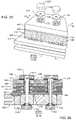
- FIG. 29is a fragmented perspective and partially exploded view of a bipolar feedthrough terminal assembly with wire bond caps
- FIG. 30is an enlarged, fragmented cross-sectional view taken generally along the line 30 - 30 of FIG. 29 ;
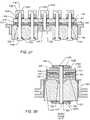
- FIG. 31is an exploded perspective view of an internally grounded dual inline 9-pole filter feedthrough capacitor hermetic terminal embodying the present invention.
- FIG. 32is a perspective view of the assembled 9-pole filter feedthrough capacitor hermetic terminal of FIG. 31 ;
- FIG. 33is an enlarged cross-sectional view taken generally along the line 33 - 33 of FIG. 32 ;
- FIG. 34is an exploded perspective view of an internally grounded quadpolar feedthrough capacitor embodying the present invention.
- FIG. 35is a perspective view of the assembled feedthrough terminal assembly of FIG. 34 ;
- FIG. 36is a cross-sectional view taken generally along the line 36 - 36 of FIG. 35 ;
- FIG. 37is a perspective view of modified L-shaped wire bond pad taken generally of the structure illustrated by the line 37 - 37 in FIG. 35 ;
- FIG. 38is a cross-sectional view of another unipolar hermetic terminal embodying the invention.
- FIG. 39is a sectional view of yet another embodiment of the invention similar to that shown in FIG. 6 , wherein the wire bond cap has been drilled and threaded.
- FIG. 6A novel method of providing a wire bond pad 150 is shown in FIG. 6 .
- a counterbored Kovar or Alloy 42 diskas also shown in FIGS. 7 and 8 , is bonded or laminated 228 onto the top of capacitor 110 over a shortened lead wire or terminal terminal pin 136 by soldering, conductive thermal-setting adhesives, resistance welding, laser welding material 154 or the like.
- FIG. 7is an isometric view of the wire bond cap 150 and FIG. 8 is a cross-sectional view of the wire bond cap 150 of FIG. 6 .
- wire bond cap 150as shown in FIGS. 6 and 7 would be constructed of Kovar or Alloy 42.
- the Kovarwould be nickel plated and then over plated with soft gold suitable for compatibility with ultrasonic, thermal or thermal sonic wire bonding processes.
- Electrical connection material 154is preferably placed in shear between the wire bond pad 150 and the terminal terminal pin 136 . This is essential to form a highly reliable electrical connection that will withstand the vibration and shock forces associated with subsequent ultrasonic wire bond attachment(s). This shear area is accomplished by the counterbore area 152 shown in FIGS. 7 and 8 .
- the wire bond cap 150 of FIG. 7is also described in pending U.S. patent application Ser. Nos. 10/377,018, 10/377,272 and 10/377,086.
- an alternative method of forming the electrical connection 154 between the counterbore 152 of wire bond cap 150 and terminal terminal pin 136is by prior art resistance welding techniques.
- the counterbore 152 of wire bond cap 150would fit very tightly onto terminal pin 136 .
- Electrical contactswould be placed on the outside diameter of wire bond cap 150 and a current pulse from the resistance weld machine would be applied sufficient to cause heating and reflow of metals and/or the plating of wire bond cap 150 to form a low resistance metallurgical bond to terminal pin 136 .
- electrical connection material 154also makes a reliable and oxide free electrical connection to the gold braze area 132 .
- the gold braze material 132penetrates through any surface oxidation on terminal pin 136 , for example, if terminal pin 136 is niobium or tantalum, and thereby forms a highly conductive and reliable hermetic seal connection.
- electrical connection material 154also makes an electrical connection to the inside diameter metallization 116 of feedthrough capacitor 110 and to the gold plated counterbore area 152 of the Kovar wire bond cap 150 .
- terminal pin 136can be of any biocompatible material including oxidized materials such as niobium, and that no pretreatment, for example, sputter coating, is required to make a reliable electrical connection from terminal pin 136 to the feedthrough capacitor inside diameter metallization 116 or to the gold plated wire bond cap 150 . In other words, no direct electrical contact from the capacitor inside termination 116 or the wire bond cap 150 is required to terminal pin 136 .
- FIG. 6is a Table which specifies the properties of a thermal plastic polyimide supported tape adhesive 228 which is ideal for laminating the bond pad 150 of the present invention to the ceramic capacitor 110 or insulator 134 surface.
- the industry designation for thisis ABLELOC®5500.
- Thisis the same polyimide supported tape adhesive 128 that is generally used to bond the ceramic capacitor 110 to the surface of the hermetic terminal 122 .
- This materialis convenient in that it can be die cut, stamped or laser cut into convenient geometries to co-bond a bonding pad 150 or an induction, or an alumina substrate 140 to the capacitor 110 or bond the capacitor to a hermetic terminal 122 .
- polyimideis an ideal high-temperature material that will readily withstand the installation stresses into the implantable medical device caused by laser welding. A number of other bonding materials can also be used including adhesives, epoxies, glasses and the like.
- a wire bond pad 150is also connected to the end of the terminal terminal pin 136 on the body fluid side, as illustrated in FIG. 6 .
- a connection of the wire bond pad 150 to the terminal terminal pin 136 and the illumine insulator 134can be made in the same manner, as described above.
- the purpose of the hermetic terminalis to allow conductive terminal pins 136 to pass in nonconductive relationship through the titanium housing or can 124 of the pacemaker or implantable cardioverter defibrillator. Accordingly, all materials used on the body fluid side of such can or housing must be biocompatible. This limits the materials that can be used to noble metals, titanium, stainless steel and the like. Usually the terminal terminal pin 136 would be of platinum, platinum-iridium alloy, tantalum, niobium or the like.
- the terminal pin 136is platinum or platinum-iridium, these are highly solderable materials and therefore, it is easy to form a well wetted solder joint or conductive polymer connection between the bond pad 150 and the outside diameter of the terminal terminal pin 136 .
- the terminal pinis constructed of tantalum or niobium, these materials are generally not easily wetted by solder or conductive polymers. This can complicate the solder or conductive polymer joint. This is because niobium and tantalum form a heavy oxide layer on their surfaces. Accordingly, a niobium or tantalum terminal pin 136 must be pretreated so that a solder joint or connection with a conductive thermal setting material can be accomplished.
- U.S. Pat. No. 6,159,560describes a method of depositing silver on a tantalum pin to displace surface oxide and deposit a conductive finish suitable for making an electrical connection.
- pin metal coating methodologiesincluding sputter or vacuum deposition (as described in U.S. Pat. No. 5,531,003), of materials such as gold, titanium and other conductors which can then be followed up with surface plating with gold, iridium or the like.
- the wire bond pad 150could be resistance welded to the tip of the terminal terminal pin 136 as described above.
- FIG. 9illustrates another embodiment of the present invention.
- Mechanically robust and reliable metallurgical jointsare preferred and are generally of the group of laser welding, brazing and the like.
- a preferred embodiment illustrated in FIG. 9overcomes such deficiencies with a wire bond pad 250 that has been modified to accommodate laser beam welding.
- the terminal pinscan be of niobium or tantalum construction instead of relatively expensive platinum or platinum-iridium alloys.
- Niobium and tantalumare notorious for forming heavy oxides on their surface and generally do not readily accept solder or thermal setting conductive adhesives.
- Previous methods of making the electrical contact with niobium or tantalum lead wiresinclude an expensive process of pre-treating the niobium with vacuum or sputter deposition processes or other metallic overcoating. Such overcoat materials can be platinum, gold and the like.
- FIG. 9overcomes all of these previous deficiencies with the novel assembly method as illustrated.
- FIG. 9is similar to the unipolar hermetic terminal assembly of FIG. 3 with a metallic ferrule 122 . Co-bonded to this assembly is a prior art ceramic feedthrough capacitor 110 .
- the ferrule 122is designed to be laser welded 156 into the housing 124 of an implantable medical device such as a cardiac pacemaker or implantable cardioverter defibrillator (ICD).
- Gold braze 130forms a hermetic seal connection between the ferrule 122 and the alumina insulator 134 .
- the gold braze material 132makes the hermetic connection between the terminal terminal pin 136 and the hermetic alumina insulator 134 .
- the alumina insulator 134could be replaced by a variety of glasses or other sealing materials.
- the mounting of the unipolar capacitor 110 to this terminalis in accordance with prior art U.S. Pat. No. 5,333,095 and others.
- FIG. 9one can see that the alumina substrate 240 of the present invention is placed on top and co-bonded 228 to the ceramic capacitor 110 .
- a counterbored wire bond cap 250is placed over the top of the co-bonded alumina substrate 240 as shown. It is a novel aspect of the Kovar cap that it have one or more side through holes 158 .
- holes 158are designed so that a laser beam from a laser welder can be directed into the through hole 158 to impinge its energy upon the terminal pin 136 . Accordingly, a highly reliable laser weld connection 160 is formed between the counterbored wire bond cap 250 and the terminal terminal pin 136 .
- a highly reliable laser weld connection 160is formed between the counterbored wire bond cap 250 and the terminal terminal pin 136 .
- another wire bond pad 250with the same arrangement as described above is laser welded 160 to the terminal terminal pin 136 extending out from the housing 124 of the implantable device and into the body fluid. This enables lead wires and the like to be attached directly to the wire bond pad 250 , and extend to the organ in question, such as the heart, or other devices and the like.
- FIG. 9Another novel aspect of the assembly shown in FIG. 9 is the fact that no electrical connection is needed from the inside diameter termination 116 of the feedthrough capacitor 110 and the terminal pin 136 . This is because there is an electrical connection from a bottom termination surface 162 of the feedthrough capacitor 110 to a corresponding top termination surface 164 of the alumina substrate 240 .
- the electrical connection material 166 joining these two surfacescan be solder, conductive thermal setting adhesives and the like.
- the wire bond cap 250has been previously gold brazed 168 to a metallized surface 170 of the alumina substrate 240 as shown.
- the wire bond cap 250is first gold brazed using a gold braze preform 168 to the metallization 170 that is on the surface of the alumina substrate 240 .
- the laser weld 160is then made by projecting a laser beam through the holes 158 in the wire bond cap 250 .
- FIG. 10is an inverted isometric view of the feedthrough capacitor 110 .
- An important featureis the circular surface metallization band 162 which forms a continuous electrical connection with the inside diameter termination 116 .
- the capacitor 110would be tumbled either in the green or fired state prior to metallization application so that the sharp transmission corner from the passage hole to the surface is rounded. This makes for a more reliable electrical connection between the top circular metallization 162 and the inside diameter metallization 116 .
- FIG. 11is an enlarged cross-section taken along line 11 - 11 of FIG. 10 , which illustrates the rounded corner 172 .
- a sharp, non-tumbled square cornercould cause the metallization 116 - 162 to pull away during firing and becoming undesirably thin and discontinuous at the sharp edge. Such condition could lead to high resistance or even loss of circuit continuity.
- the alumina substrate 240has an inside diameter or via hole metallization 144 which forms a continuous electrical connection with a similar circular metallization stripe 164 .
- FIG. 13illustrates an alternative embodiment of the alumina substrate 240 of FIG. 12 which incorporates a circular boss 174 into which a counterbore holds an electrical connection material 166 . This boss also appears in FIG. 9 .
- Electrical connection material 166can be either a thermal setting conductive adhesive, solder a gold braze preform or the like. This gold brazed preform 166 is designed to seat against the metallized surface 164 of the alumina substrate 240 .
- the wire bond cap 250is pre-assembled by gold braze 168 to a circular metallized band 170 on the opposite side of the alumina substrate 240 as shown in FIGS. 9 , 12 and 13 .
- the capacitor circular metallization band 162is electrically connected through material 166 to the corresponding metallization band 164 of the alumina substrate 240 .
- the wire bond cap 250is gold brazed to the opposite side metallization surface 170 of the alumina substrate 240 , there is then a continuous electrical connection from the inside diameter metallization of the feedthrough capacitor 116 through the inside diameter via hole metallization 144 of the substrate 240 all the way to its top metallization 170 and in turn, to the wire bond cap 250 .
- the rest of the electrical circuitis completed by the laser weld connection between the wire bond cap 250 and the terminal terminal pin 136 shown as 160 .
- Another advantageis the ability to pre-assemble the wire bond cap 250 to the alumina substrate 240 to the feedthrough capacitor 110 and test and inventory this piece as a sub-assembly.
- the most expensive part of the hermetically sealed filtered terminalis the hermetic seal feedthrough 178 without a capacitor 110 .
- Thisconsists of the assembly of the terminal terminal pin 136 to the alumina insulator 134 to the ferrule 122 which is hermetically and mechanically connected by gold brazes 130 and 132 . In this way, a large quantity of the hermetic terminal assemblies can be built and kept in inventory. A quantity of the pre-assemblies can also be built and kept in inventory.
- the capacitance value determined by the feedthrough capacitor 110varies anywhere in human implant applications from 25 picofarads to around 9000 picofarads. In one cardiac pacemaker application alone, the capacitance value can vary from approximately 1000-9000 picofarads. Accordingly, it is an advantage to be able to inventory various capacitance values of the pre-assembly and keep them in inventory ready to be installed by co-bonding 128 and laser welding to the hermetic terminal and then final tested and shipped.
- the wire bond pad 250has had its laser through hole 158 ′ enlarged at the opening point.
- Thiscan be done by a counter sink, counterbore or the like. In this way, it is easier to direct the laser beam energy against terminal pin 136 thereby facilitating formation of the laser weld connection 160 between the wire bond cap 250 and the terminal terminal pin 136 . This can be done on one or more sides around the circumference of the wire bond cap.
- the laser weld hole 158 ′shown in FIG. 14 , has a counterbore which enlarges the opening for the laser beam.
- the terminal pin 136can be of a non-wettable material such as niobium or tantalum.
- an electrical connection material 168which attaches the wire bond cap 250 directly to the capacitor top metallization 162 .
- Capacitor top metallization 162is continuous and also forms a termination surface 116 all around the inside diameter of the capacitor 110 feedthrough hole. The capacitor 110 depicted in FIG. 14 requires no additional electrical connection between the terminal terminal pin 136 and the feedthrough capacitor inside diameter termination 116 .
- connection material 168is directly attached to the alumina insulator 134 , which connection can be made in a variety of ways, including connection material 168 , an adhesive-backed washer, polyimide or other non-conductive adhesive or the like.
- FIG. 14Aillustrates an alternative method of attaching the wire bond cap 250 to the top metallization 162 of the ceramic capacitor 110 .
- wire bond cap 250is attached to the top capacitor metallization 162 through a sandwiched electrical connection consisting of either gold braze, solder, conductive thermosetting adhesives or the like.
- the electrical connection materialhas been relocated as shown.
- 168 ′would typically not be a gold braze but of the group of solder, conductive polyimide or conductive epoxy.
- FIG. 15illustrates an alternative embodiment of the wire bond cap 250 of FIG. 14 .
- a laser weld joint 160is formed in the same manner as previously described for FIG. 14 .
- the electrical connection material 168 ′is only between the terminal pin 136 and the capacitor inside diameter metallization 116 .
- FIG. 16is a cross-sectional view of the EMI filtered hermetic terminal of FIG. 9 modified with two improvements.
- Ring 184has been previously gold brazed to the metallization 170 of the alumina ceramic substrate 340 making a solid mechanical and electrical connection.
- the terminal terminal pin 136is then attached by laser welding 160 to the metallic ring 184 .
- Laser weldingmakes a very reliable and rugged electrical and mechanical joint in this important series connection.
- Non-ceramic printed circuit board materialscan also be used as a circuit board substitute for the ceramic substrate of the present invention and are mostly constructed from a resin reinforced by a fabric cloth. Epoxy (FR-4), polyimide and cyanate ester are the more common resin systems in use today. Fiberglass is the most popular fabric. It is important that the circuit board substrate be able to withstand the high temperatures caused by laser welding of the EMI filtered hermetic terminal assembly with wire bonds into the housing of an implantable medical device.
- Non-ceramic circuit board temperature rangeis most often expressed as the glass transition temperature (Tg) of the material.
- Tgglass transition temperature
- Printed circuit board materialschange from hard, brittle substances to soft, rubber like substances after they reach their glass transition temperature. Typical Tg ratings for the more common material systems are as follows:
- Tg Polyimides260° C.-270° C.
- Modified Polymidies240° C.-260° C. Cyanate Esters 240° C.-250° C. BT* Epoxies 225° C.-240° C.
- Composite Epoxies240° C.-260° C. MultiFunctional EpoxieS 160° C.-190° C. TetraFunctional Epoxies 140° C.-160° C.
- Photo-resist, chemical etching, automated screen printing, silk screening, selective plating, screen printing and thin or thick film deposition methodsare typically used to lay down the conductive circuit trace patterns, the bond pads or “lands” and the location and metallization of via holes.
- Binder PhaseTo hold the ink to the ceramic substrate, and merges with the ceramic during high temperature firing.
- Substrate via holesare typically formed by automated pattern recognition drilling machines. There are a number of methods of providing metallization on the circuit paths, the bonding pads and through the via holes, including screen printing selective plating, metallization vacuum pull through, screen printing, cladding followed by selective etching, physical vapor deposition (PVD), chemical vapor deposition (CVD), and the like. Since these techniques are well known in the art, they will not be completely described herein.
- FIG. 20is a cross-sectional view from FIG. 19 which better illustrates the mounting of the wire bond pad 450 .
- wire bond pad 450has been electrically and mechanically attached to the circuit trace 146 using braze preform 148 .
- This brazing operationwould typically be performed on the alumina substrate 340 in a high temperature vacuum-brazing furnace.
- the braze joints 168 and 148 of FIG. 16which attaches the ring 184 to the alumina substrate metallization 170 and the wire bond pad 450 to the alumina substrate 340 metallization 146 would typically be done prior to capacitor bonding at the same time in vacuum brazing furnace re-flow operation.
- FIG. 17is an enlarged cross-sectional view from area “17” of FIG. 16 , also illustrating the mounting of a wire bond pad 450 to the alumina insulator 134 using a circuit trace 146 .
- the terminal pin 136can be of both solderable or heavily oxidized materials.
- terminal terminal pin 136can be of the group of niobium, tantalum, titanium or other heavily oxidized materials. Normally, such heavily oxidized materials are not readily wettable with solder or suitable for attachment using a thermal setting conductive adhesive.
- solderable or heavily oxidized materialsare not readily wettable with solder or suitable for attachment using a thermal setting conductive adhesive.
- a similar electrical connection from the insert ring 184 to the terminal pin 136is formed by the laser welding material 160 .
- This laser weldalso burns through any surface oxide on niobium, tantalum, or titanium pins and the like, thereby making a highly reliable electrical connection from the terminal pin 136 to the ring 184 which has been previously gold brazed to the surface metallization 170 , of substrate 340 .
- the novel feedthrough capacitor with substrate as described in FIG. 16has a number of advantages, including the obvious one of having highly reliable brazed electrical connections, and being suitable for wire bonding, but also suitable for use with literally any type of biocompatible terminal pin 136 .
- FIG. 21illustrates a cross-sectional view of the present invention with an L-shaped wire bond cap 550 .
- This wire bond pad 550is typically Kovar or Alloy 42 and is gold plated.
- FIG. 21is the cross-section of a wire bonded lead wire 186 .
- the attachment of lead wire 186 to the L-shaped wire bond pad 550is better seen in isometric view FIG. 22 .
- lead wire 186which is routed to internal implanted medical device circuitry, has been wire bonded in the area shown as 188 to the wire bond pad 550 . It is typical in the art that lead wire 186 be a small diameter, pure gold or aluminum wire, such as a wire 0.005 inches in diameter.
- the wire bond connection 188is typically formed by ultrasonic or thermosonic processes that are very well known in the art.
- an L-shaped wire bond cap 550is bonded to the alumina insulator 134 , and has a conductive connection 160 to the terminal pin 136 .
- a lead wire 186is attached thereto, such as by ultrasonic or thermosonic processes, and extends to a location outside of the device, such as an organ within the body.
- FIG. 23shows an alternative embodiment to that previously described in FIG. 21 .
- the wire bond pad 550has been directly attached to the top of the ceramic feedthrough capacitor 110 .
- the wire bond pad 550is electrically and mechanically attached to the top of the ceramic capacitor using a conductive thermal setting polymer 138 , a gold braze or a solder 168 .
- a laser weld connection 160is formed between lead wire 136 and the wire bond pad 550 as shown.
- FIG. 23is a lower cost alternative, but is not considered to be as mechanically robust as having an alumina or equivalent material substrate 140 placed between the wire bond pad 550 and the ceramic capacitor 110 .
- the ultrasonic wire bonding forces that would be applied during the attachment of the lead wire 186would put substantial mechanical stress onto the relatively fragile ceramic capacitor 110 itself. This must be a highly controlled process so that microfractures are not induced into the ceramic capacitor 110 . Such microfractures have been shown to cause immediate or latent failure (electrical short circuit) of capacitor 110 . Such short circuiting could be life threatening to a pacemaker patient.
- FIG. 24is an isometric view of the L-shaped wire bond pad 550 , previously described in FIG. 23 .
- FIG. 25is a similar wire bond pad 550 ′ as described in FIG. 24 , except that it is angled ( ⁇ ) to line up with the geometry or architecture of the internal circuits of the implanted medical device. As shown in FIG. 25 , any convenient angle ( ⁇ ) can be used.
- FIG. 29illustrates the top view of a bipolar capacitor of the present invention.
- exploded away circular wire bond pads 650are placed over the top of the feedthrough holes of substrate 440 for convenient attachment of lead wires 186 (not shown). This is better understood by observing the cross-section of FIG. 29 illustrated in FIG. 30 .
- a circular wire bond pad 650is attached to the top surface via metallization 170 of the ceramic substrate 440 .
- the attachment of the circular wire bond pad 650is by gold brazing 168 to the top metallization 170 of the alumina substrate 440 .
- the terminal pin 136which comes from the hermetic terminal consisting of 122 , 130 , 132 , 136 and 134 , is shortened as shown.
- the alumina substrate 440is co-bonded using a nonconductive polyimide preform 228 to the top surface of the ceramic capacitor 210 .
- the electrical connection material 138is typically a conductive thermal setting polymer, such as a conductive polyimide, solder or the like.
- the electrical connection material 138electrically connects the inside diameter or via hole metallization 144 of the substrate 440 to the terminal pin 136 and in turn to the inside diameter metallization 116 of the feedthrough capacitor 210 .
- wire bond pads 650are conductively coupled to the terminal pins 136 via metallization 170 or the like. This enables the attachment to of lead wires (not shown) directly to these wire bonding pads 650 on the body fluid side of the device.
- lead wiresnot shown
- materials on the body fluid side, including the wire bonding pads 650must be comprised of a biocompatible material, such as a noble metal, stainless steel, titanium or the like.
- FIG. 31illustrates an exploded view of an internally grounded dual inline 9-pole filtered feedthrough capacitor 510 hermetic terminal of the present invention.
- the wire bond pads 750which are typically of gold plated Kovar or the like, on both the body fluid side as well as the side to be disposed within the active medical implant device.
- the alumina substrate 740has convenient recesses and metallized areas 164 (typically of gold or nickel coated tungsten) suitable for metallurgical connection via gold brazing material or preforms 168 to the wire bond pads 750 .
- An adhesive coated polyimide nonconductive preform 228bonds the alumina substrate 740 to the ceramic feedthrough capacitor 510 .
- internally grounded feedthrough capacitorsare well known in the art.
- ground pin 236be centered to provide a low inductance path to the feedthrough capacitor active electrode plates (not shown). Accordingly, ground pin 236 has been centrally located and solidly welded, gold brazed or machined into the metallic ferrule 122 , as illustrated in FIG. 32 . All of the other pins 136 are in nonconductive relationship with the ferrule 122 as previously described in the prior art.
- FIG. 32illustrates a perspective view of the completed assembly of FIG. 31 .
- convenient wire bond attachmentcan be made to the wire bond pads 750 .
- FIG. 32is a cross-sectional view of the 9-pole internally grounded feedthrough capacitor of FIG. 32 .
- laser weld connection 160is made between each wire bond pad 750 and the corresponding terminal pin 136 .
- the wire bonding pads 750are conductively coupled, such as by weld 160 , to opposite ends of the terminal pins 136 , as illustrated in FIG. 33 .
- Thisenables lead wires to be connected both internally and externally of the active implantable medical device housing and be conductively coupled to the terminal pin 136 , which is hermetically sealed and yet provides electric conductivity through the hermetic assembly.
- feedthrough capacitors 510can be utilized to remove potentially damaging EMI.
- FIG. 34illustrates an exploded view of an internally grounded quadpolar plus ground pin hermetic terminal for human implant applications.
- the internally grounded feedthrough assemblyhas four active feedthrough pins 136 and one ground pin 236 .
- the ground pin 236is shown welded to ferrule 122 in the center which is desirable, such as for use as a convenient ground point. This is because terminal pin 236 is brazed or welded directly to the ferrule 122 of the assembly. In many cases, a ground to the titanium housing 124 is required.
- a grounded wire bond pad 550 ′as illustrated in FIGS. 34-36 , this avoids the need to provide a special grounding location on the titanium housing of the implantable medical device.
- FIG. 35illustrates the completed assembly of FIG. 34 .
- a lead wire 186is shown wire bonded 188 to one of the wire bond pads 550 .
- Wire bonding equipmentincluding automated systems with robotic controls typically have a rather large feed head through which the wire to be bonded protrudes.
- the wire bond equipment feed headtapers to a point and is somewhat conical in cross-section.
- substrate 1540has been tapered down into area 216 thereby providing sufficient space for the wire bond head to come in and properly engage the leads 186 and wire bond pads 550 .
- Thisis a novel aspect of the present invention that can be adapted to many other of the substrates that are described in this patent application.
- the center wire bond pad 550 ′is grounded to ferrule 122 of the hermetic terminal.
- terminal pin 236is both mechanically and electrically connected to the center of overall metallic ferrule structure 122 .
- Wire bond pad 550 ′is not necessary in all implantable medical devices. In certain cardiac pacemakers and implantable defibrillators, a convenient grounding location is an important feature. For example, in an implantable defibrillator cardioverter, where the titanium housing of the device can also be a cardiac shock electrode, a low resistance connection must be made from the high voltage output circuitry of the implantable defibrillator to its overall titanium housing 124 . Accordingly, wire bond pad 550 ′ provides a convenient place to make such a connection. The rest of this shock electrode circuit is completed by laser welding the ferrule 122 into the overall housing or titanium shield 124 of the implantable medical device (not shown).
- FIG. 36illustrates a cross-sectional view of the quadpolar plus ground pin assembly of FIG. 35 .
- the wire bond pads 550have been attached by brazing material 202 to the top metallization 146 of the alumina substrate 1540 .
- a laser weld connection 160is made between terminal pin 136 and the wire bond pad 550 or 550 ′.
- Wire bond pads 1150can be placed on the other side of the hermetic terminal assembly and are brazed 230 directly to the alumina insulator 134 .
- Human body fluidis very corrosive.
- the wire bond pads 550 or 1150 , the braze 230 and the underlying lead material 136must be of suitable biocompatible material.
- Such materialsinclude the group of platinum, niobium, gold, tantalum, titanium, stainless and their various alloys including alloys containing iridium and nickel.
- Attachment of lead wires 186 (not shown) to the body fluid side wire bond padsis preferably done by direct lead wire welding or brazing. These lead wires would typically connect from the wire bond pads 1150 to the connector or header block (not shown) of a cardiac pacemaker and the like. If attachment to wire bond pads 1150 is by mechanical attachment, ultrasonic bonding or thermosonic bonding, then wire bond pads 1150 would either be of gold or would require an ultra-pure gold over plating.
- laser welds 130 and 132make a mechanical and hermetic seal connection between alumina insulator 134 and both the ferrule 122 and terminal pin 136 .
- Manufacturing of the unipolar EMI filter capacitor assembly as shown in FIG. 38is relatively simple. All that is involved is to drop capacitor 110 over terminal pin 136 and then also place wire bond cap 1250 on top of capacitor 110 . Fixturing would then apply pressure to center and push down on wire bond pad 1250 while automated equipment formed the laser weld 160 as shown. At this point the ceramic capacitor is captured between the pedestal area 234 of the alumina insulator 134 and the wire bond pad 1250 .
- thermosetting conductive polymer 2126 and 126both around the outside diameter of the Kovar pad 1250 and the capacitor outside diameter termination 112 as shown.
- the connection material 2126makes electrical contact between the wire bond pad 1250 and the top metallization ring 162 of the ceramic capacitor 110 .
- the top metallization ring 162forms a continuous electrical connection to the capacitor inside diameter metallization 116 and to the active electrodes 118 of the feedthrough capacitor 110 .
- a wire bond pad 1250 on the body fluid sidecan be welded to the terminal pin 136 and attached to the alumina insulator 134 in the same manner.
- electrical connection material 126makes an electrical contact between the outside diameter termination 112 of the feedthrough capacitor 110 and the gold braze area 130 of the hermetic terminal ferrule 122 .
- the outside diameter metallization 112 of the capacitor 110is electrically connected to its ground electrode plates 120 .
- Co-pending U.S. patent application Ser. No. 10/377,086describes the importance of making electrical contact to a gold surface instead of directly to the titanium ferrule 122 . This is because titanium is notorious for forming oxides which could preclude the proper performance of the EMI filter at high frequency.
- An alternative method of assembling the unipolar capacitor 110 shown in FIG. 38would be to first pre-assemble the wire bond cap 1250 to the ceramic capacitor 110 by making the mechanical and electrical connection 2126 to the top metallization 162 of the feedthrough capacitor 110 . In this way the capacitor and Kovar pad assembly could be tested and then stored in inventory. When it came time to attach this pre-assembly to the hermetic terminal, all that would need to be done is to mount the assembly in place and perform the laser weld 160 to terminal pins and make the electrical connection 126 ground the capacitor outside diameter termination 112 as previously described.
- the assembly of FIG. 38does not incorporate the nonconductive bonding washers 228 used in previously described embodiments. This results in a space or air gap 235 between the wire bond cap 1250 and the capacitor 110 . This gap is very small but could present a concern where contaminants could be trapped. Accordingly, the assembly of FIG. 38 is best suited for low voltage pacemaker applications.
- wire bond cap 1250has a central through hole where the laser weld connection 160 is made to lead wire 136 . This reduces the top surface contact area of the wire bond pad 1250 that is available for subsequent wire bonding to the lead wires.
- FIG. 39an alternative method of attaching wire bond cap 1450 is illustrated.
- FIG. 39is similar to FIG. 6 .
- the novel wire bond cap 1450has been drilled and threaded 1451 as shown. This is designed to mate up with a threaded portion 1449 of terminal pin 136 .
- Such threadscan typically be formed using screw machines and the like.
- opposite ends of the terminal pin 136include external threads such that a wire bond cap 1450 can be threadedly inserted onto the ends for attachment to lead wires either extending from the internal circuitry within the housing 124 of the device, or externally on the body fluid side of the device.
- the threaded-on wire bond cap 1450is typically constructed of Kovar or Alloy 42 which is then nickel plated and then over plated with pure gold suitable for wire bonding.
- the shape of the wire bond cap of 1450can be circular, rectangular, hexagonal or any other shape to fit a convenient tool for screwing the device into place.
- a bonding washer(not shown) could be used sandwiched between the threaded wire bond cap 1450 and the top surface of the ceramic capacitor 110 . After threading the wire bond cap 1450 into place, this washer could be cured which would firmly seat the threaded cap into position so that it would be able to withstand shock and vibration forces.
Landscapes
- Engineering & Computer Science (AREA)
- Power Engineering (AREA)
- Health & Medical Sciences (AREA)
- Animal Behavior & Ethology (AREA)
- Radiology & Medical Imaging (AREA)
- Life Sciences & Earth Sciences (AREA)
- Nuclear Medicine, Radiotherapy & Molecular Imaging (AREA)
- General Health & Medical Sciences (AREA)
- Public Health (AREA)
- Veterinary Medicine (AREA)
- Biomedical Technology (AREA)
- Manufacturing & Machinery (AREA)
- Microelectronics & Electronic Packaging (AREA)
- Electrotherapy Devices (AREA)
Abstract
Description
| Tg | ||
| Polyimides | 260° C.-270° C. | ||
| Modified | 240° C.-260° | ||
| Cyanate Esters | |||
| 240° C.-250° C. | |||
| BT* Epoxies | 225° C.-240° | ||
| Composite Epoxies | |||
| 240° C.-260° | |||
| MultiFunctional EpoxieS | |||
| 160° C.-190° | |||
| TetraFunctional Epoxies | |||
| 140° C.-160° C. | |||
| Modified FR*-4′ | 120° C.-130° C. | ||
| Standard FR*-4′ | 115° C.-125° C. | ||
| BT = Barium Titanate | |||
| FR = fiber reinforced | |||
| Functional Phase | Consists of metal powders (Pt, Pd, Ag, Au, |
| etc.) in conductive inks, metals and/or metal | |
| oxides (RuO2, Bi2Ru2O7, Pd, Ag) in resistors | |
| and ceramic/glass (BaTiO3, glass) in dielectric | |
| temperature firing. | |
| Binder Phase | To hold the ink to the ceramic substrate, and |
| merges with the ceramic during high | |
| temperature firing. | |
| Vehicle | Acts as the carrier for the powders and is |
| composed of both volatile (solvents) and | |
| non-volatile (polymers) organics. These | |
| evaporate and burn off during the early | |
| stages of drying and firing, respectively. | |
| Modifiers | Are small amounts of proprietary additives |
| which control behavior of the inks before and | |
| after processing. | |
- 1. Conductor Pastes—Single metal systems (such as, Pd, Ag, Au, Ni, etc.).
- 2. Conductor Pastes—Binary metal systems (such as, Ag/Pd, Ag/Pt, etc), Tungsten (W), Tungsten/Nickel and equivalent.
- 3. Conductor Pastes—Ternary metal systems (such as, 40 Au/40 Pd/20 Pt, 60 Ag/20 Pt/20 Pd, 35 Ag/25 Pd/20 Au/20 Pt, etc.).
- 4. High fire systems (such as, 30 Ag/70 Pd with BaTiO3or ZrO additives, 100 Pd, etc.).
- 5. Base metal systems (such as, Ni with BaTiO3or ZrO additives, etc.)
Claims (58)
Priority Applications (1)
| Application Number | Priority Date | Filing Date | Title |
|---|---|---|---|
| US11/308,662US7623335B2 (en) | 2003-02-27 | 2006-04-19 | Hermetic feedthrough terminal assembly with wire bond pads for human implant applications |
Applications Claiming Priority (9)
| Application Number | Priority Date | Filing Date | Title |
|---|---|---|---|
| US10/377,272US6765780B2 (en) | 2002-02-28 | 2003-02-27 | EMI feedthrough filter terminal assembly having surface mounted, internally grounded hybrid capacitor |
| US10/377,018US6888715B2 (en) | 2002-02-28 | 2003-02-27 | EMI feedthrough filter terminal assembly utilizing hermetic seal for electrical attachment between lead wires and capacitor |
| US10/377,086US6765779B2 (en) | 2002-02-28 | 2003-02-27 | EMI feedthrough filter terminal assembly for human implant applications utilizing oxide resistant biostable conductive pads for reliable electrical attachments |
| US50842603P | 2003-10-02 | 2003-10-02 | |
| US54877004P | 2004-02-27 | 2004-02-27 | |
| US10/825,900US6999818B2 (en) | 2003-05-23 | 2004-04-15 | Inductor capacitor EMI filter for human implant applications |
| US10/842,967US7038900B2 (en) | 2003-02-27 | 2004-05-10 | EMI filter terminal assembly with wire bond pads for human implant applications |
| US11/182,289US7310216B2 (en) | 2003-02-27 | 2005-07-14 | EMI filter terminal assembly with wire bond pads for human implant applications |
| US11/308,662US7623335B2 (en) | 2003-02-27 | 2006-04-19 | Hermetic feedthrough terminal assembly with wire bond pads for human implant applications |
Related Parent Applications (1)
| Application Number | Title | Priority Date | Filing Date |
|---|---|---|---|
| US11/182,289Continuation-In-PartUS7310216B2 (en) | 2003-02-27 | 2005-07-14 | EMI filter terminal assembly with wire bond pads for human implant applications |
Publications (2)
| Publication Number | Publication Date |
|---|---|
| US20060259093A1 US20060259093A1 (en) | 2006-11-16 |
| US7623335B2true US7623335B2 (en) | 2009-11-24 |
Family
ID=37420161
Family Applications (1)
| Application Number | Title | Priority Date | Filing Date |
|---|---|---|---|
| US11/308,662Expired - LifetimeUS7623335B2 (en) | 2003-02-27 | 2006-04-19 | Hermetic feedthrough terminal assembly with wire bond pads for human implant applications |
Country Status (1)
| Country | Link |
|---|---|
| US (1) | US7623335B2 (en) |
Cited By (30)
| Publication number | Priority date | Publication date | Assignee | Title |
|---|---|---|---|---|
| US20080039709A1 (en)* | 2004-08-09 | 2008-02-14 | Karmarkar Parag V | Implantable Mri compatible Stimulation Leads And Antennas And Related Systems And Methods |
| US20080097193A1 (en)* | 2004-07-27 | 2008-04-24 | Karmarkar Parag V | Mri Systems Having Mri Compatible Universal Delivery Cannulas With Cooperating Mri Antenna Probes and Related Systems and Methods |
| US20080119919A1 (en)* | 2001-04-13 | 2008-05-22 | Surgi-Vision, Inc. | Mri compatible medical leads with band stop filters |
| US20080243218A1 (en)* | 2007-03-19 | 2008-10-02 | Bottomley Paul A | Mri and rf compatible leads and related methods of operating and fabricating leads |
| US20080262584A1 (en)* | 2007-03-19 | 2008-10-23 | Bottomley Paul A | Methods and apparatus for fabricating leads with conductors and related flexible lead configurations |
| US20090171421A1 (en)* | 2005-10-21 | 2009-07-02 | Ergin Atalar | Mri-safe high impedance lead systems |
| US20110082531A1 (en)* | 2009-10-05 | 2011-04-07 | Swanson Lawrence D | Side mount feedthrough system for sealed components |
| US20110218422A1 (en)* | 2005-05-04 | 2011-09-08 | Surgivision, Inc. | Electrical lead for an electronic device such as an implantable device |
| US8219208B2 (en) | 2001-04-13 | 2012-07-10 | Greatbatch Ltd. | Frequency selective passive component networks for active implantable medical devices utilizing an energy dissipating surface |
| US8275466B2 (en) | 2006-06-08 | 2012-09-25 | Greatbatch Ltd. | Band stop filter employing a capacitor and an inductor tank circuit to enhance MRI compatibility of active medical devices |
| US20120261183A1 (en)* | 2011-04-15 | 2012-10-18 | Bernd Pretzlaff | Lead feedthrough and electrical functional unit |
| US8478409B2 (en) | 2007-03-21 | 2013-07-02 | Medtronic, Inc. | Filtering capacitor feedthrough assembly |
| EP2617461A1 (en) | 2012-01-16 | 2013-07-24 | Greatbatch Ltd. | Co-fired hermetically sealed feedthrough with alumina substrate and platinum filled via for an active implantable medical device |
| WO2014151141A1 (en)* | 2013-03-15 | 2014-09-25 | The Charles Stark Draper Laboratory, Inc. | Methods for bonding a hermetic module to an electrode array |
| US9093974B2 (en)* | 2012-09-05 | 2015-07-28 | Avx Corporation | Electromagnetic interference filter for implanted electronics |
| EP3320950A1 (en) | 2016-11-10 | 2018-05-16 | Greatbatch Ltd. | Feedthrough assembly for active implantable medical device |
| EP3326692A1 (en) | 2016-11-08 | 2018-05-30 | Greatbatch Ltd. | Feedthrough for an implantable medical device having a composite conductive lead |
| EP3345652A1 (en) | 2017-01-06 | 2018-07-11 | Greatbatch Ltd. | Method for manufacturing a feedthrough for an active implantable medical device |
| EP3449973A1 (en) | 2017-08-30 | 2019-03-06 | Greatbatch Ltd. | Hermetically sealed filtered feedthrough assembly |
| US10249415B2 (en) | 2017-01-06 | 2019-04-02 | Greatbatch Ltd. | Process for manufacturing a leadless feedthrough for an active implantable medical device |
| US10350421B2 (en) | 2013-06-30 | 2019-07-16 | Greatbatch Ltd. | Metallurgically bonded gold pocket pad for grounding an EMI filter to a hermetic terminal for an active implantable medical device |
| US10449375B2 (en) | 2016-12-22 | 2019-10-22 | Greatbatch Ltd. | Hermetic terminal for an AIMD having a pin joint in a feedthrough capacitor or circuit board |
| US10561837B2 (en) | 2011-03-01 | 2020-02-18 | Greatbatch Ltd. | Low equivalent series resistance RF filter for an active implantable medical device utilizing a ceramic reinforced metal composite filled via |
| US10874865B2 (en) | 2017-11-06 | 2020-12-29 | Avx Corporation | EMI feedthrough filter terminal assembly containing a resin coating over a hermetically sealing material |
| US10905888B2 (en) | 2018-03-22 | 2021-02-02 | Greatbatch Ltd. | Electrical connection for an AIMD EMI filter utilizing an anisotropic conductive layer |
| US10912945B2 (en) | 2018-03-22 | 2021-02-09 | Greatbatch Ltd. | Hermetic terminal for an active implantable medical device having a feedthrough capacitor partially overhanging a ferrule for high effective capacitance area |
| US20210051812A1 (en)* | 2014-12-24 | 2021-02-18 | Medtronic, Inc. | Hermetically-sealed packages including feedthrough assemblies |
| US11198014B2 (en) | 2011-03-01 | 2021-12-14 | Greatbatch Ltd. | Hermetically sealed filtered feedthrough assembly having a capacitor with an oxide resistant electrical connection to an active implantable medical device housing |
| US11351387B2 (en) | 2012-01-16 | 2022-06-07 | Greatbatch Ltd. | Method of manufacturing a singulated feedthrough insulator for a hermetic seal of an active implantable medical device incorporating a post conductive paste filled pressing step |
| US12302492B2 (en) | 2020-12-16 | 2025-05-13 | Neuropace, Inc. | Interposer for active implantable medical device |
Families Citing this family (70)
| Publication number | Priority date | Publication date | Assignee | Title |
|---|---|---|---|---|
| US6701176B1 (en) | 1998-11-04 | 2004-03-02 | Johns Hopkins University School Of Medicine | Magnetic-resonance-guided imaging, electrophysiology, and ablation |
| US9295828B2 (en) | 2001-04-13 | 2016-03-29 | Greatbatch Ltd. | Self-resonant inductor wound portion of an implantable lead for enhanced MRI compatibility of active implantable medical devices |
| WO2002083016A1 (en) | 2001-04-13 | 2002-10-24 | Surgi-Vision, Inc. | Systems and methods for magnetic-resonance-guided interventional procedures |
| US6904307B2 (en) | 2002-05-29 | 2005-06-07 | Surgi-Vision, Inc. | Magnetic resonance probes |
| US20070260282A1 (en)* | 2003-09-12 | 2007-11-08 | Taylor William J | Feedthrough apparatus with noble metal-coated leads |
| US7966070B2 (en)* | 2003-09-12 | 2011-06-21 | Medtronic, Inc. | Feedthrough apparatus with noble metal-coated leads |
| US20060247714A1 (en)* | 2005-04-28 | 2006-11-02 | Taylor William J | Glass-to-metal feedthrough seals having improved durability particularly under AC or DC bias |
| US7340305B2 (en)* | 2005-06-09 | 2008-03-04 | Cardiac Pacemakers, Inc. | Implantable medical device feedthrough assembly having a coated conductor |
| US7656031B2 (en)* | 2007-02-05 | 2010-02-02 | Bridge Semiconductor Corporation | Stackable semiconductor package having metal pin within through hole of package |
| US7502217B2 (en)* | 2007-02-16 | 2009-03-10 | Medtronic, Inc. | Filtering capacitor feedthrough assembly |
| US8373384B2 (en)* | 2007-04-11 | 2013-02-12 | Pacesetter, Inc. | Capacitor-integrated feedthrough assembly with improved grounding for an implantable medical device |
| US8160708B2 (en)* | 2007-04-11 | 2012-04-17 | Pacesetter, Inc. | Capacitor-integrated feedthrough assembly with improved grounding for an implantable medical device |
| US7693576B1 (en) | 2007-04-11 | 2010-04-06 | Pacesetter, Inc. | Capacitor-integrated feedthrough assembly for an implantable medical device |
| US20090082832A1 (en)* | 2007-09-25 | 2009-03-26 | Boston Scientific Neuromodulation Corporation | Thermal Management of Implantable Medical Devices |
| US8165694B2 (en)* | 2008-01-29 | 2012-04-24 | Boston Scientific Neuromodulation Corporation | Thermal management of implantable medical devices |
| US9108066B2 (en) | 2008-03-20 | 2015-08-18 | Greatbatch Ltd. | Low impedance oxide resistant grounded capacitor for an AIMD |
| CN102037528A (en)* | 2008-03-20 | 2011-04-27 | 格瑞巴奇有限公司 | Shielded three-terminal flat-through EMI/energy dissipating filter |
| US10080889B2 (en) | 2009-03-19 | 2018-09-25 | Greatbatch Ltd. | Low inductance and low resistance hermetically sealed filtered feedthrough for an AIMD |
| US20090270956A1 (en)* | 2008-04-25 | 2009-10-29 | Pacesetter, Inc. | Implantable medical lead configured for improved mri safety |
| US20090281592A1 (en)* | 2008-05-08 | 2009-11-12 | Pacesetter, Inc. | Shaft-mounted rf filtering elements for implantable medical device lead to reduce lead heating during mri |
| US8332037B2 (en) | 2008-11-05 | 2012-12-11 | Incube Labs, Llc | Housing structure for a medical implant including a monolithic substrate |
| US20110094768A1 (en)* | 2009-10-28 | 2011-04-28 | Pacesetter, Inc. | Implantable medical device having feedthru with an integrated interconnect/filter substrate |
| US8648255B2 (en)* | 2010-05-21 | 2014-02-11 | Greatbatch Ltd. | Laser beam button weld of dissimilar materials |
| EP2651510B1 (en)* | 2010-12-15 | 2015-11-04 | Advanced Bionics AG | Particulate toughened ceramic feedthrough |
| DE102011009865B4 (en) | 2011-01-31 | 2012-09-20 | Heraeus Precious Metals Gmbh & Co. Kg | Headboard for a medically implantable device |
| DE102011009859B4 (en) | 2011-01-31 | 2012-09-20 | Heraeus Precious Metals Gmbh & Co. Kg | Ceramic bushing with filter |
| DE102011009857B8 (en)* | 2011-01-31 | 2013-01-17 | Heraeus Precious Metals Gmbh & Co. Kg | Electrical feedthrough with a cermet-like connector for an active implantable medical device |
| DE102011009860B4 (en) | 2011-01-31 | 2013-03-07 | Heraeus Precious Metals Gmbh & Co. Kg | Implantable device with integrated ceramic bushing |
| DE102011009858B8 (en) | 2011-01-31 | 2013-11-07 | Heraeus Precious Metals Gmbh & Co. Kg | Cermet-containing bushing for a medically implantable device with a bonding layer |
| DE102011009861B4 (en) | 2011-01-31 | 2012-09-20 | Heraeus Precious Metals Gmbh & Co. Kg | Process for the preparation of a cermet-containing feedthrough |
| DE102011009867B4 (en) | 2011-01-31 | 2013-09-05 | Heraeus Precious Metals Gmbh & Co. Kg | Ceramic bushing for a medically implantable device |
| DE102011009856B8 (en) | 2011-01-31 | 2012-12-27 | W.C. Heraeus Gmbh | An electrical feedthrough and method of making a lead-containing feedthrough for a medically implantable device |
| DE102011009866B4 (en) | 2011-01-31 | 2013-09-05 | Heraeus Precious Metals Gmbh & Co. Kg | Directly applied electrical feedthrough |
| DE102011009863B9 (en) | 2011-01-31 | 2020-08-13 | Heraeus Deutschland GmbH & Co. KG | Ceramic bushing with line elements of high conductivity |
| DE102011009862B4 (en) | 2011-01-31 | 2012-11-08 | Heraeus Precious Metals Gmbh & Co. Kg | Cermet-containing bushing with holding element for a medically implantable device |
| DE102011009855B8 (en) | 2011-01-31 | 2013-01-03 | Heraeus Precious Metals Gmbh & Co. Kg | Ceramic bushing with inductive filter |
| US9427596B2 (en) | 2013-01-16 | 2016-08-30 | Greatbatch Ltd. | Low impedance oxide resistant grounded capacitor for an AIMD |
| US9931514B2 (en) | 2013-06-30 | 2018-04-03 | Greatbatch Ltd. | Low impedance oxide resistant grounded capacitor for an AIMD |
| US8694102B2 (en)* | 2011-03-09 | 2014-04-08 | Greatbatch Ltd. | Ionizing radiation-protected active implantable medical device |
| WO2012158845A2 (en)* | 2011-05-16 | 2012-11-22 | Lawrence Livermore National Security, Llc | Method of fabricating high-density hermetic electrical feedthroughs using insulated wire bundles |
| US9627833B2 (en)* | 2011-08-02 | 2017-04-18 | Medtronic, Inc. | Electrical leads for a feedthrough |
| US8670829B2 (en) | 2011-08-02 | 2014-03-11 | Medtronic, Inc. | Insulator for a feedthrough |
| US8841558B2 (en) | 2011-08-02 | 2014-09-23 | Medtronic Inc. | Hermetic feedthrough |
| US9724524B2 (en) | 2011-08-02 | 2017-08-08 | Medtronic, Inc. | Interconnection of conductor to feedthrough |
| US8872035B2 (en) | 2011-08-02 | 2014-10-28 | Medtronic, Inc. | Hermetic feedthrough |
| US8588916B2 (en)* | 2011-08-02 | 2013-11-19 | Medtronic, Inc. | Feedthrough configured for interconnect |
| US8593816B2 (en) | 2011-09-21 | 2013-11-26 | Medtronic, Inc. | Compact connector assembly for implantable medical device |
| DE102011119125B4 (en) | 2011-11-23 | 2014-01-23 | Heraeus Precious Metals Gmbh & Co. Kg | Contacting arrangement with bushing and filter structure |
| US8648328B2 (en)* | 2011-12-27 | 2014-02-11 | Sharp Laboratories Of America, Inc. | Light emitting diode (LED) using three-dimensional gallium nitride (GaN) pillar structures with planar surfaces |
| US9889306B2 (en) | 2012-01-16 | 2018-02-13 | Greatbatch Ltd. | Hermetically sealed feedthrough with co-fired filled via and conductive insert for an active implantable medical device |
| US10046166B2 (en) | 2012-01-16 | 2018-08-14 | Greatbatch Ltd. | EMI filtered co-connected hermetic feedthrough, feedthrough capacitor and leadwire assembly for an active implantable medical device |
| US10881867B2 (en) | 2012-01-16 | 2021-01-05 | Greatbatch Ltd. | Method for providing a hermetically sealed feedthrough with co-fired filled via for an active implantable medical device |
| US20150250386A1 (en)* | 2012-09-28 | 2015-09-10 | Csem Centre Suisse D'electronique Et De Microtechnique Sa -Recherche Et Developpement | Implantable devices |
| USRE46699E1 (en) | 2013-01-16 | 2018-02-06 | Greatbatch Ltd. | Low impedance oxide resistant grounded capacitor for an AIMD |
| US9478959B2 (en) | 2013-03-14 | 2016-10-25 | Heraeus Deutschland GmbH & Co. KG | Laser welding a feedthrough |
| US9431801B2 (en) | 2013-05-24 | 2016-08-30 | Heraeus Deutschland GmbH & Co. KG | Method of coupling a feedthrough assembly for an implantable medical device |
| US9403023B2 (en) | 2013-08-07 | 2016-08-02 | Heraeus Deutschland GmbH & Co. KG | Method of forming feedthrough with integrated brazeless ferrule |
| US9504841B2 (en) | 2013-12-12 | 2016-11-29 | Heraeus Deutschland GmbH & Co. KG | Direct integration of feedthrough to implantable medical device housing with ultrasonic welding |
| US9610451B2 (en) | 2013-12-12 | 2017-04-04 | Heraeus Deutschland GmbH & Co. KG | Direct integration of feedthrough to implantable medical device housing using a gold alloy |
| US9610452B2 (en) | 2013-12-12 | 2017-04-04 | Heraeus Deutschland GmbH & Co. KG | Direct integration of feedthrough to implantable medical device housing by sintering |
| EP3826104B1 (en) | 2014-09-22 | 2023-05-03 | Tc1 Llc | Antenna designs for communication between a wirelessly powered implant to an external device outside the body |
| US9865533B2 (en)* | 2014-12-24 | 2018-01-09 | Medtronic, Inc. | Feedthrough assemblies |
| US9968794B2 (en) | 2014-12-24 | 2018-05-15 | Medtronic, Inc. | Implantable medical device system including feedthrough assembly and method of forming same |
| KR101656723B1 (en)* | 2015-06-30 | 2016-09-12 | 재단법인 오송첨단의료산업진흥재단 | Feedthrough making method |
| US10098589B2 (en) | 2015-12-21 | 2018-10-16 | Medtronic, Inc. | Sealed package and method of forming same |
| US10726998B2 (en)* | 2016-01-08 | 2020-07-28 | Energizer Brands, Llc | Feedthrough device |
| EP3228354B1 (en) | 2016-04-07 | 2020-08-05 | Heraeus Deutschland GmbH & Co. KG | Method of directly connecting a wire to a feedthrough comprising a cermet conductor and an associated feedthrough |
| EP3384958A1 (en)* | 2017-04-03 | 2018-10-10 | BIOTRONIK SE & Co. KG | Feedthrough for implant components |
| EP4226968B1 (en) | 2020-02-21 | 2025-04-30 | Heraeus Medical Components, LLC | Ferrule for non-planar medical device housing |
| EP3900782B1 (en) | 2020-02-21 | 2023-08-09 | Heraeus Medical Components, LLC | Ferrule with strain relief spacer for implantable medical device |
Citations (45)
| Publication number | Priority date | Publication date | Assignee | Title |
|---|---|---|---|---|
| US2756375A (en) | 1952-02-06 | 1956-07-24 | Sprague Electric Co | Feed-through capacitors |
| US3235939A (en) | 1962-09-06 | 1966-02-22 | Aerovox Corp | Process for manufacturing multilayer ceramic capacitors |
| US3538464A (en) | 1963-08-20 | 1970-11-03 | Erie Technological Prod Inc | Multiple pin connector having ferrite core stacked capacitor filter |
| US3920888A (en) | 1974-06-04 | 1975-11-18 | Nuclear Battery Corp | Electrical feed-through assembly suitable for electronic devices implantable in a human body |
| US4083022A (en) | 1976-10-12 | 1978-04-04 | Bunker Ramo Corporation | Planar pi multi-filter having a ferrite inductance for pin filters in electrical connectors |
| US4144509A (en) | 1977-01-12 | 1979-03-13 | Bunker Ramo Corporation | Filter connector |
| US4148003A (en) | 1977-07-08 | 1979-04-03 | Globe-Union Inc. | Series feed-through capacitor |
| US4152540A (en) | 1977-05-03 | 1979-05-01 | American Pacemaker Corporation | Feedthrough connector for implantable cardiac pacer |
| US4220813A (en) | 1977-09-26 | 1980-09-02 | Medical Components Corp. | Terminal for medical instrument |
| US4247881A (en) | 1979-04-02 | 1981-01-27 | Sprague Electric Company | Discoidal monolithic ceramic capacitor |
| US4314213A (en) | 1978-03-30 | 1982-02-02 | Murata Manufacturing Co., Ltd. | Through-type capacitor |
| US4352951A (en) | 1977-09-26 | 1982-10-05 | Medical Components Corp. | Ceramic seals between spaced members such as a terminal pin and a ferrule |
| US4362792A (en) | 1980-12-01 | 1982-12-07 | Emerson Electric Co. | Conductor seal assembly |
| US4424551A (en) | 1982-01-25 | 1984-01-03 | U.S. Capacitor Corporation | Highly-reliable feed through/filter capacitor and method for making same |
| US4456786A (en) | 1979-11-19 | 1984-06-26 | James C. Kyle | Terminal assembly for heart pacemaker |
| US4737601A (en) | 1986-08-18 | 1988-04-12 | Dynawave Incorporated | Hermetically sealed electrical feedthrough and method of making same |
| US4741710A (en) | 1986-11-03 | 1988-05-03 | Amphenol Corporation | Electrical connector having a monolithic capacitor |
| US5032692A (en) | 1989-05-09 | 1991-07-16 | Avx Corporation | Process for manufactoring hermetic high temperature filter packages and the products produced thereby |
| US5070605A (en) | 1988-04-22 | 1991-12-10 | Medtronic, Inc. | Method for making an in-line pacemaker connector system |
| US5142430A (en) | 1990-03-28 | 1992-08-25 | Anthony Anthony A | Power line filter and surge protection circuit components and circuits |
| US5333095A (en) | 1993-05-03 | 1994-07-26 | Maxwell Laboratories, Inc., Sierra Capacitor Filter Division | Feedthrough filter capacitor assembly for human implant |
| US5440447A (en) | 1993-07-02 | 1995-08-08 | The Morgan Crucible Company, Plc | High temperature feed-through system and method for making same |
| US5539611A (en) | 1991-05-26 | 1996-07-23 | Endress U Hauser Gmbh U Co. | Interface connection through an insulating part |
| US5650759A (en) | 1995-11-09 | 1997-07-22 | Hittman Materials & Medical Components, Inc. | Filtered feedthrough assembly having a mounted chip capacitor for medical implantable devices and method of manufacture therefor |
| US5751539A (en) | 1996-04-30 | 1998-05-12 | Maxwell Laboratories, Inc. | EMI filter for human implantable heart defibrillators and pacemakers |
| US5759197A (en) | 1994-10-04 | 1998-06-02 | Medtronic, Inc. | Protective feedthrough |
| US5825608A (en) | 1996-10-18 | 1998-10-20 | Novacap, Inc. | Feed-through filter capacitor assembly |
| US5836992A (en) | 1994-10-04 | 1998-11-17 | Medtronic, Inc. | Filtered feedthrough assembly for implantable medical device |
| US5867361A (en) | 1997-05-06 | 1999-02-02 | Medtronic Inc. | Adhesively-bonded capacitive filter feedthrough for implantable medical device |
| US5905627A (en) | 1997-09-10 | 1999-05-18 | Maxwell Energy Products, Inc. | Internally grounded feedthrough filter capacitor |
| US5959829A (en) | 1998-02-18 | 1999-09-28 | Maxwell Energy Products, Inc. | Chip capacitor electromagnetic interference filter |
| US5973906A (en) | 1998-03-17 | 1999-10-26 | Maxwell Energy Products, Inc. | Chip capacitors and chip capacitor electromagnetic interference filters |
| US6008980A (en) | 1997-11-13 | 1999-12-28 | Maxwell Energy Products, Inc. | Hermetically sealed EMI feedthrough filter capacitor for human implant and other applications |
| US6414835B1 (en) | 2000-03-01 | 2002-07-02 | Medtronic, Inc. | Capacitive filtered feedthrough array for an implantable medical device |
| US6459935B1 (en) | 2000-07-13 | 2002-10-01 | Avx Corporation | Integrated filter feed-thru |
| US6529103B1 (en)* | 2000-09-07 | 2003-03-04 | Greatbatch-Sierra, Inc. | Internally grounded feedthrough filter capacitor with improved ground plane design for human implant and other applications |
| US6545854B2 (en) | 2001-05-25 | 2003-04-08 | Presidio Components, Inc. | Fringe-field non-overlapping-electrodes discoidal feed-through ceramic filter capacitor with high breakdown voltage |
| US6619763B2 (en) | 2001-05-25 | 2003-09-16 | Presidio Components, Inc. | Feed-through filter capacitor with non-overlapping electrodes |
| US6765780B2 (en)* | 2002-02-28 | 2004-07-20 | Greatbatch-Sierra, Inc. | EMI feedthrough filter terminal assembly having surface mounted, internally grounded hybrid capacitor |
| US6985347B2 (en) | 2002-02-28 | 2006-01-10 | Greatbatch-Sierra, Inc. | EMI filter capacitors designed for direct body fluid exposure |
| US6987660B2 (en)* | 2003-02-27 | 2006-01-17 | Greatbatch-Sierra, Inc. | Spring contact system for EMI filtered hermetic seals for active implantable medical devices |
| US6999818B2 (en)* | 2003-05-23 | 2006-02-14 | Greatbatch-Sierra, Inc. | Inductor capacitor EMI filter for human implant applications |
| US7035077B2 (en)* | 2004-05-10 | 2006-04-25 | Greatbatch-Sierra, Inc. | Device to protect an active implantable medical device feedthrough capacitor from stray laser weld strikes, and related manufacturing process |
| US7136273B2 (en)* | 2005-03-30 | 2006-11-14 | Greatbatch-Sierra, Inc. | Hybrid spring contact system for EMI filtered hermetic seals for active implantable medical devices |
| US7145076B2 (en)* | 2005-02-08 | 2006-12-05 | Greatbatch, Inc. | Method for minimizing stress in feedthrough capacitor filter assemblies |
- 2006
- 2006-04-19USUS11/308,662patent/US7623335B2/ennot_activeExpired - Lifetime
Patent Citations (51)
| Publication number | Priority date | Publication date | Assignee | Title |
|---|---|---|---|---|
| US2756375A (en) | 1952-02-06 | 1956-07-24 | Sprague Electric Co | Feed-through capacitors |
| US3235939A (en) | 1962-09-06 | 1966-02-22 | Aerovox Corp | Process for manufacturing multilayer ceramic capacitors |
| US3538464A (en) | 1963-08-20 | 1970-11-03 | Erie Technological Prod Inc | Multiple pin connector having ferrite core stacked capacitor filter |
| US3920888A (en) | 1974-06-04 | 1975-11-18 | Nuclear Battery Corp | Electrical feed-through assembly suitable for electronic devices implantable in a human body |
| US4083022A (en) | 1976-10-12 | 1978-04-04 | Bunker Ramo Corporation | Planar pi multi-filter having a ferrite inductance for pin filters in electrical connectors |
| US4144509A (en) | 1977-01-12 | 1979-03-13 | Bunker Ramo Corporation | Filter connector |
| US4152540A (en) | 1977-05-03 | 1979-05-01 | American Pacemaker Corporation | Feedthrough connector for implantable cardiac pacer |
| US4148003A (en) | 1977-07-08 | 1979-04-03 | Globe-Union Inc. | Series feed-through capacitor |
| US4220813A (en) | 1977-09-26 | 1980-09-02 | Medical Components Corp. | Terminal for medical instrument |
| US4352951A (en) | 1977-09-26 | 1982-10-05 | Medical Components Corp. | Ceramic seals between spaced members such as a terminal pin and a ferrule |
| US4314213A (en) | 1978-03-30 | 1982-02-02 | Murata Manufacturing Co., Ltd. | Through-type capacitor |
| US4247881A (en) | 1979-04-02 | 1981-01-27 | Sprague Electric Company | Discoidal monolithic ceramic capacitor |
| US4456786A (en) | 1979-11-19 | 1984-06-26 | James C. Kyle | Terminal assembly for heart pacemaker |
| US4362792A (en) | 1980-12-01 | 1982-12-07 | Emerson Electric Co. | Conductor seal assembly |
| US4424551A (en) | 1982-01-25 | 1984-01-03 | U.S. Capacitor Corporation | Highly-reliable feed through/filter capacitor and method for making same |
| US4424551B1 (en) | 1982-01-25 | 1991-06-11 | Highly-reliable feed through/filter capacitor and method for making same | |
| US4737601A (en) | 1986-08-18 | 1988-04-12 | Dynawave Incorporated | Hermetically sealed electrical feedthrough and method of making same |
| US4741710A (en) | 1986-11-03 | 1988-05-03 | Amphenol Corporation | Electrical connector having a monolithic capacitor |
| US5070605A (en) | 1988-04-22 | 1991-12-10 | Medtronic, Inc. | Method for making an in-line pacemaker connector system |
| US5032692A (en) | 1989-05-09 | 1991-07-16 | Avx Corporation | Process for manufactoring hermetic high temperature filter packages and the products produced thereby |
| US5142430A (en) | 1990-03-28 | 1992-08-25 | Anthony Anthony A | Power line filter and surge protection circuit components and circuits |
| US5670063A (en) | 1991-05-26 | 1997-09-23 | Endress + Hauser Gmbh + Co. | Method for making an interface connection through an insulating part |
| US5539611A (en) | 1991-05-26 | 1996-07-23 | Endress U Hauser Gmbh U Co. | Interface connection through an insulating part |
| US5333095A (en) | 1993-05-03 | 1994-07-26 | Maxwell Laboratories, Inc., Sierra Capacitor Filter Division | Feedthrough filter capacitor assembly for human implant |
| US5440447A (en) | 1993-07-02 | 1995-08-08 | The Morgan Crucible Company, Plc | High temperature feed-through system and method for making same |
| US5759197A (en) | 1994-10-04 | 1998-06-02 | Medtronic, Inc. | Protective feedthrough |
| US5836992A (en) | 1994-10-04 | 1998-11-17 | Medtronic, Inc. | Filtered feedthrough assembly for implantable medical device |
| US5650759A (en) | 1995-11-09 | 1997-07-22 | Hittman Materials & Medical Components, Inc. | Filtered feedthrough assembly having a mounted chip capacitor for medical implantable devices and method of manufacture therefor |
| US5751539A (en) | 1996-04-30 | 1998-05-12 | Maxwell Laboratories, Inc. | EMI filter for human implantable heart defibrillators and pacemakers |
| US5825608A (en) | 1996-10-18 | 1998-10-20 | Novacap, Inc. | Feed-through filter capacitor assembly |
| US6031710A (en) | 1997-05-06 | 2000-02-29 | Medtronic, Inc. | Adhesively- and solder-bonded capacitive filter feedthrough for implantable medical devices |
| US5867361A (en) | 1997-05-06 | 1999-02-02 | Medtronic Inc. | Adhesively-bonded capacitive filter feedthrough for implantable medical device |
| US5870272A (en) | 1997-05-06 | 1999-02-09 | Medtronic Inc. | Capacitive filter feedthrough for implantable medical device |
| US5905627A (en) | 1997-09-10 | 1999-05-18 | Maxwell Energy Products, Inc. | Internally grounded feedthrough filter capacitor |
| US6008980A (en) | 1997-11-13 | 1999-12-28 | Maxwell Energy Products, Inc. | Hermetically sealed EMI feedthrough filter capacitor for human implant and other applications |
| US5959829A (en) | 1998-02-18 | 1999-09-28 | Maxwell Energy Products, Inc. | Chip capacitor electromagnetic interference filter |
| US5973906A (en) | 1998-03-17 | 1999-10-26 | Maxwell Energy Products, Inc. | Chip capacitors and chip capacitor electromagnetic interference filters |
| US6414835B1 (en) | 2000-03-01 | 2002-07-02 | Medtronic, Inc. | Capacitive filtered feedthrough array for an implantable medical device |
| US20020166618A1 (en) | 2000-03-01 | 2002-11-14 | Medtronic, Inc. | Capacitive filtered feedthrough array for an implantable medical device |
| US6459935B1 (en) | 2000-07-13 | 2002-10-01 | Avx Corporation | Integrated filter feed-thru |
| US6566978B2 (en)* | 2000-09-07 | 2003-05-20 | Greatbatch-Sierra, Inc. | Feedthrough capacitor filter assemblies with leak detection vents |
| US6529103B1 (en)* | 2000-09-07 | 2003-03-04 | Greatbatch-Sierra, Inc. | Internally grounded feedthrough filter capacitor with improved ground plane design for human implant and other applications |
| US6545854B2 (en) | 2001-05-25 | 2003-04-08 | Presidio Components, Inc. | Fringe-field non-overlapping-electrodes discoidal feed-through ceramic filter capacitor with high breakdown voltage |
| US6619763B2 (en) | 2001-05-25 | 2003-09-16 | Presidio Components, Inc. | Feed-through filter capacitor with non-overlapping electrodes |
| US6765780B2 (en)* | 2002-02-28 | 2004-07-20 | Greatbatch-Sierra, Inc. | EMI feedthrough filter terminal assembly having surface mounted, internally grounded hybrid capacitor |
| US6985347B2 (en) | 2002-02-28 | 2006-01-10 | Greatbatch-Sierra, Inc. | EMI filter capacitors designed for direct body fluid exposure |
| US6987660B2 (en)* | 2003-02-27 | 2006-01-17 | Greatbatch-Sierra, Inc. | Spring contact system for EMI filtered hermetic seals for active implantable medical devices |
| US6999818B2 (en)* | 2003-05-23 | 2006-02-14 | Greatbatch-Sierra, Inc. | Inductor capacitor EMI filter for human implant applications |
| US7035077B2 (en)* | 2004-05-10 | 2006-04-25 | Greatbatch-Sierra, Inc. | Device to protect an active implantable medical device feedthrough capacitor from stray laser weld strikes, and related manufacturing process |
| US7145076B2 (en)* | 2005-02-08 | 2006-12-05 | Greatbatch, Inc. | Method for minimizing stress in feedthrough capacitor filter assemblies |
| US7136273B2 (en)* | 2005-03-30 | 2006-11-14 | Greatbatch-Sierra, Inc. | Hybrid spring contact system for EMI filtered hermetic seals for active implantable medical devices |
Cited By (66)
| Publication number | Priority date | Publication date | Assignee | Title |
|---|---|---|---|---|
| US20080119919A1 (en)* | 2001-04-13 | 2008-05-22 | Surgi-Vision, Inc. | Mri compatible medical leads with band stop filters |
| US8219208B2 (en) | 2001-04-13 | 2012-07-10 | Greatbatch Ltd. | Frequency selective passive component networks for active implantable medical devices utilizing an energy dissipating surface |
| US20080097193A1 (en)* | 2004-07-27 | 2008-04-24 | Karmarkar Parag V | Mri Systems Having Mri Compatible Universal Delivery Cannulas With Cooperating Mri Antenna Probes and Related Systems and Methods |
| US8108028B2 (en) | 2004-07-27 | 2012-01-31 | Surgi-Vision Inc. | MRI systems having MRI compatible universal delivery cannulas with cooperating MRI antenna probes and related systems and methods |
| US8509876B2 (en) | 2004-08-09 | 2013-08-13 | The Johns Hopkins University | Implantable MRI compatible stimulation leads and antennas and related systems and methods |
| US20080039709A1 (en)* | 2004-08-09 | 2008-02-14 | Karmarkar Parag V | Implantable Mri compatible Stimulation Leads And Antennas And Related Systems And Methods |
| US8649842B2 (en) | 2005-05-04 | 2014-02-11 | Boston Scientific Neuromodulation Corporation | Electrical lead for an electronic device such as an implantable device |
| US20110218422A1 (en)* | 2005-05-04 | 2011-09-08 | Surgivision, Inc. | Electrical lead for an electronic device such as an implantable device |
| US8380277B2 (en) | 2005-05-04 | 2013-02-19 | MRI Interventions, Inc. | Electrical lead for an electronic device such as an implantable device |
| US8055351B2 (en) | 2005-10-21 | 2011-11-08 | Boston Scientific Neuromodulation Corporation | MRI-safe high impedance lead systems |
| US20090171421A1 (en)* | 2005-10-21 | 2009-07-02 | Ergin Atalar | Mri-safe high impedance lead systems |
| US8688226B2 (en) | 2005-10-21 | 2014-04-01 | Boston Scientific Neuromodulation Corporation | MRI-safe high impedance lead systems |
| US8433421B2 (en) | 2005-10-21 | 2013-04-30 | Boston Scientific Neuromodulation Corporation | MRI-safe high impedance lead systems |
| US8275466B2 (en) | 2006-06-08 | 2012-09-25 | Greatbatch Ltd. | Band stop filter employing a capacitor and an inductor tank circuit to enhance MRI compatibility of active medical devices |
| US9119968B2 (en) | 2006-06-08 | 2015-09-01 | Greatbatch Ltd. | Band stop filter employing a capacitor and an inductor tank circuit to enhance MRI compatibility of active medical devices |
| US9630000B2 (en) | 2007-03-19 | 2017-04-25 | Boston Scientific Neuromodulation Corporation | Methods and apparatus for fabricating leads with conductors and related flexible lead configurations |
| US10391307B2 (en) | 2007-03-19 | 2019-08-27 | Boston Scientific Neuromodulation Corporation | MRI and RF compatible leads and related methods of operating and fabricating leads |
| US9492651B2 (en) | 2007-03-19 | 2016-11-15 | MRI Interventions, Inc. | MRI and RF compatible leads and related methods of operating and fabricating leads |
| US20080262584A1 (en)* | 2007-03-19 | 2008-10-23 | Bottomley Paul A | Methods and apparatus for fabricating leads with conductors and related flexible lead configurations |
| US9248270B2 (en) | 2007-03-19 | 2016-02-02 | Boston Scientific Neuromodulation Corporation | Methods and apparatus for fabricating leads with conductors and related flexible |
| US20080243218A1 (en)* | 2007-03-19 | 2008-10-02 | Bottomley Paul A | Mri and rf compatible leads and related methods of operating and fabricating leads |
| US8478409B2 (en) | 2007-03-21 | 2013-07-02 | Medtronic, Inc. | Filtering capacitor feedthrough assembly |
| US8954150B2 (en) | 2009-10-05 | 2015-02-10 | Cardiac Pacemakers, Inc. | Side mount feedthrough system for sealed components |
| US20110082531A1 (en)* | 2009-10-05 | 2011-04-07 | Swanson Lawrence D | Side mount feedthrough system for sealed components |
| US10596369B2 (en) | 2011-03-01 | 2020-03-24 | Greatbatch Ltd. | Low equivalent series resistance RF filter for an active implantable medical device |
| US10561837B2 (en) | 2011-03-01 | 2020-02-18 | Greatbatch Ltd. | Low equivalent series resistance RF filter for an active implantable medical device utilizing a ceramic reinforced metal composite filled via |
| US11344734B2 (en) | 2011-03-01 | 2022-05-31 | Greatbatch Ltd. | Filtered feedthrough assembly having a capacitor ground metallization electrically connected to the gold braze portion sealing a ferrule peninsula to a matching insulator cutout |
| US11198014B2 (en) | 2011-03-01 | 2021-12-14 | Greatbatch Ltd. | Hermetically sealed filtered feedthrough assembly having a capacitor with an oxide resistant electrical connection to an active implantable medical device housing |
| US11071858B2 (en) | 2011-03-01 | 2021-07-27 | Greatbatch Ltd. | Hermetically sealed filtered feedthrough having platinum sealed directly to the insulator in a via hole |
| US8941020B2 (en)* | 2011-04-15 | 2015-01-27 | Litronik Entwicklungs Gmbh | Lead feedthrough and electrical functional unit |
| US20120261183A1 (en)* | 2011-04-15 | 2012-10-18 | Bernd Pretzlaff | Lead feedthrough and electrical functional unit |
| EP3366348A1 (en) | 2012-01-16 | 2018-08-29 | Greatbatch Ltd. | Emi filtered co-connected hermetic feedthrough, feedthrough capacitor and leadwire assembly for an active implantable medical device |
| EP2628504A1 (en) | 2012-01-16 | 2013-08-21 | Greatbatch Ltd. | EMI filtered co-connected hermetic feedthrough, feedthrough capacitor and leadwire assembly for an active implantable medical device |
| US11351387B2 (en) | 2012-01-16 | 2022-06-07 | Greatbatch Ltd. | Method of manufacturing a singulated feedthrough insulator for a hermetic seal of an active implantable medical device incorporating a post conductive paste filled pressing step |
| EP2636427A1 (en) | 2012-01-16 | 2013-09-11 | Greatbatch Ltd. | Elevated hermetic feedthrough insulator adapted for side attachment of electrical conductors on the body fluid side of an active implantable medical device |
| EP2617461A1 (en) | 2012-01-16 | 2013-07-24 | Greatbatch Ltd. | Co-fired hermetically sealed feedthrough with alumina substrate and platinum filled via for an active implantable medical device |
| US9093974B2 (en)* | 2012-09-05 | 2015-07-28 | Avx Corporation | Electromagnetic interference filter for implanted electronics |
| US10154616B2 (en) | 2012-09-05 | 2018-12-11 | Avx Corporation | Electromagnetic interference filter for implanted electronics |
| WO2014151141A1 (en)* | 2013-03-15 | 2014-09-25 | The Charles Stark Draper Laboratory, Inc. | Methods for bonding a hermetic module to an electrode array |
| US9583458B2 (en) | 2013-03-15 | 2017-02-28 | The Charles Stark Draper Laboratory, Inc. | Methods for bonding a hermetic module to an electrode array |
| US9984994B2 (en) | 2013-03-15 | 2018-05-29 | The Charles Stark Draper Laboratory, Inc. | Method for bonding a hermetic module to an electrode array |
| US10350421B2 (en) | 2013-06-30 | 2019-07-16 | Greatbatch Ltd. | Metallurgically bonded gold pocket pad for grounding an EMI filter to a hermetic terminal for an active implantable medical device |
| US11950387B2 (en)* | 2014-12-24 | 2024-04-02 | Medtronic, Inc. | Methods for forming hermetically-sealed packages including feedthrough assemblies |
| US20210051812A1 (en)* | 2014-12-24 | 2021-02-18 | Medtronic, Inc. | Hermetically-sealed packages including feedthrough assemblies |
| US10272252B2 (en) | 2016-11-08 | 2019-04-30 | Greatbatch Ltd. | Hermetic terminal for an AIMD having a composite brazed conductive lead |
| EP3326692A1 (en) | 2016-11-08 | 2018-05-30 | Greatbatch Ltd. | Feedthrough for an implantable medical device having a composite conductive lead |
| EP3838337A1 (en) | 2016-11-08 | 2021-06-23 | Greatbatch Ltd. | Insulative feedthrough for an active implantable medical device (aimd) |
| EP3520857A1 (en) | 2016-11-08 | 2019-08-07 | Greatbatch Ltd. | Circuit board mounted filtered feedthrough assembly having a composite conductive lead for an aimd |
| US10589107B2 (en) | 2016-11-08 | 2020-03-17 | Greatbatch Ltd. | Circuit board mounted filtered feedthrough assembly having a composite conductive lead for an AIMD |
| EP3320950A1 (en) | 2016-11-10 | 2018-05-16 | Greatbatch Ltd. | Feedthrough assembly for active implantable medical device |
| US10272253B2 (en) | 2016-11-10 | 2019-04-30 | Greatbatch Ltd. | Hermetic terminal for an active implantable medical device with composite co-fired filled via and body fluid side brazed leadwire |
| US10449375B2 (en) | 2016-12-22 | 2019-10-22 | Greatbatch Ltd. | Hermetic terminal for an AIMD having a pin joint in a feedthrough capacitor or circuit board |
| US11202916B2 (en) | 2016-12-22 | 2021-12-21 | Greatbatch Ltd. | Hermetic terminal for an AIMD having a pin joint in a feedthrough capacitor or circuit board |
| EP3560553A1 (en) | 2017-01-06 | 2019-10-30 | Greatbatch Ltd. | Method for manufacturing a feedthrough for an active implantable medical device |
| EP3345652A1 (en) | 2017-01-06 | 2018-07-11 | Greatbatch Ltd. | Method for manufacturing a feedthrough for an active implantable medical device |
| US10559409B2 (en) | 2017-01-06 | 2020-02-11 | Greatbatch Ltd. | Process for manufacturing a leadless feedthrough for an active implantable medical device |
| US10249415B2 (en) | 2017-01-06 | 2019-04-02 | Greatbatch Ltd. | Process for manufacturing a leadless feedthrough for an active implantable medical device |
| EP3449973A1 (en) | 2017-08-30 | 2019-03-06 | Greatbatch Ltd. | Hermetically sealed filtered feedthrough assembly |
| US10874865B2 (en) | 2017-11-06 | 2020-12-29 | Avx Corporation | EMI feedthrough filter terminal assembly containing a resin coating over a hermetically sealing material |
| US11369800B2 (en) | 2017-11-06 | 2022-06-28 | KYOCERA AVX Components Corporation | EMI feedthrough filter terminal assembly containing a laminated insulative seal |
| US10912945B2 (en) | 2018-03-22 | 2021-02-09 | Greatbatch Ltd. | Hermetic terminal for an active implantable medical device having a feedthrough capacitor partially overhanging a ferrule for high effective capacitance area |
| US11712571B2 (en) | 2018-03-22 | 2023-08-01 | Greatbatch Ltd. | Electrical connection for a hermetic terminal for an active implantable medical device utilizing a ferrule pocket |
| US10905888B2 (en) | 2018-03-22 | 2021-02-02 | Greatbatch Ltd. | Electrical connection for an AIMD EMI filter utilizing an anisotropic conductive layer |
| US12064639B2 (en) | 2018-03-22 | 2024-08-20 | Greatbatch Ltd. | Electrical connection for an AIMD utilizing an anisotropic conductive layer |
| US12343548B2 (en) | 2018-03-22 | 2025-07-01 | Greatbatch Ltd. | Anisotropic conductive electrical connection from a conductive pathway through a ceramic casing to a circuit board electronic component housed inside the casing |
| US12302492B2 (en) | 2020-12-16 | 2025-05-13 | Neuropace, Inc. | Interposer for active implantable medical device |
Also Published As
| Publication number | Publication date |
|---|---|
| US20060259093A1 (en) | 2006-11-16 |
Similar Documents
| Publication | Publication Date | Title |
|---|---|---|
| US7623335B2 (en) | Hermetic feedthrough terminal assembly with wire bond pads for human implant applications | |
| US7038900B2 (en) | EMI filter terminal assembly with wire bond pads for human implant applications | |
| EP3326692B1 (en) | Feedthrough for an implantable medical device having a composite conductive lead | |
| USRE48348E1 (en) | Feedthrough filter capacitor assembly with internally grounded hermetic insulator | |
| US6414835B1 (en) | Capacitive filtered feedthrough array for an implantable medical device | |
| US9931514B2 (en) | Low impedance oxide resistant grounded capacitor for an AIMD | |
| US10306748B2 (en) | Filtered feedthrough assembly for implantable medical electronic devices | |
| US5870272A (en) | Capacitive filter feedthrough for implantable medical device | |
| US8059386B2 (en) | Capacitive elements and filtered feedthrough elements for implantable medical devices | |
| EP1488434B1 (en) | Emi feedthrough filter terminal assembly utilizing hermetic seal for electrical attachment between lead wires and capacitor | |
| US7928818B2 (en) | Capacitive elements and filtered feedthrough elements for implantable medical devices | |
| US20090079517A1 (en) | Novel capacitive elements and filtered feedthrough elements for implantable medical devices |
Legal Events
| Date | Code | Title | Description |
|---|---|---|---|
| AS | Assignment | Owner name:GREATBATCH-SIERRA, INC., NEVADA Free format text:ASSIGNMENT OF ASSIGNORS INTEREST;ASSIGNORS:STEVENSON, ROBERT A.;BRENDEL, RICHARD L.;FRYSZ, CHRISTINE A.;AND OTHERS;REEL/FRAME:018005/0063 Effective date:20060720 | |
| AS | Assignment | Owner name:MANUFACTURERS AND TRADERS TRUST COMPANY,NEW YORK Free format text:SECURITY INTEREST;ASSIGNOR:GREATBATCH LTD.;REEL/FRAME:020571/0205 Effective date:20070522 Owner name:MANUFACTURERS AND TRADERS TRUST COMPANY, NEW YORK Free format text:SECURITY INTEREST;ASSIGNOR:GREATBATCH LTD.;REEL/FRAME:020571/0205 Effective date:20070522 | |
| STCF | Information on status: patent grant | Free format text:PATENTED CASE | |
| AS | Assignment | Owner name:GREATBATCH LTD.,NEW YORK Free format text:ASSIGNMENT OF ASSIGNORS INTEREST;ASSIGNOR:GREATBATCH-SIERRA, INC.;REEL/FRAME:024066/0413 Effective date:20100311 | |
| AS | Assignment | Owner name:MANUFACTURERS AND TRADERS TRUST COMPANY, AS ADMINI Free format text:SECURITY AGREEMENT;ASSIGNOR:GREATBATCH LTD.;REEL/FRAME:026539/0217 Effective date:20110624 | |
| FPAY | Fee payment | Year of fee payment:4 | |
| AS | Assignment | Owner name:MANUFACTURERS AND TRADERS TRUST COMPANY, NEW YORK Free format text:SECURITY INTEREST;ASSIGNORS:GREATBATCH, INC.;GREATBATCH LTD.;ELECTROCHEM SOLUTIONS, INC.;AND OTHERS;REEL/FRAME:036980/0482 Effective date:20151027 | |
| FPAY | Fee payment | Year of fee payment:8 | |
| MAFP | Maintenance fee payment | Free format text:PAYMENT OF MAINTENANCE FEE, 12TH YEAR, LARGE ENTITY (ORIGINAL EVENT CODE: M1553); ENTITY STATUS OF PATENT OWNER: LARGE ENTITY Year of fee payment:12 | |
| AS | Assignment | Owner name:WELLS FARGO BANK, NATIONAL ASSOCIATION, AS ADMINISTRATIVE AGENT, VIRGINIA Free format text:SECURITY INTEREST;ASSIGNORS:GREATBATCH LTD.;ELECTROCHEM SOLUTIONS, INC.;LAKE REGION MEDICAL, INC.;AND OTHERS;REEL/FRAME:057468/0056 Effective date:20210902 | |
| AS | Assignment | Owner name:GREATBATCH LTD., NEW YORK Free format text:RELEASE BY SECURED PARTY;ASSIGNOR:MANUFACTURERS AND TRADERS TRUST COMPANY;REEL/FRAME:058224/0204 Effective date:20210903 | |
| AS | Assignment | Owner name:MICRO POWER ELECTRONICS, INC., NEW YORK Free format text:RELEASE BY SECURED PARTY;ASSIGNOR:MANUFACTURERS AND TRADERS TRUST COMPANY (AS ADMINISTRATIVE AGENT);REEL/FRAME:060938/0069 Effective date:20210903 Owner name:PRECIMED INC., NEW YORK Free format text:RELEASE BY SECURED PARTY;ASSIGNOR:MANUFACTURERS AND TRADERS TRUST COMPANY (AS ADMINISTRATIVE AGENT);REEL/FRAME:060938/0069 Effective date:20210903 Owner name:GREATBATCH-GLOBE TOOL, INC., NEW YORK Free format text:RELEASE BY SECURED PARTY;ASSIGNOR:MANUFACTURERS AND TRADERS TRUST COMPANY (AS ADMINISTRATIVE AGENT);REEL/FRAME:060938/0069 Effective date:20210903 Owner name:NEURONEXUS TECHNOLOGIES, INC., NEW YORK Free format text:RELEASE BY SECURED PARTY;ASSIGNOR:MANUFACTURERS AND TRADERS TRUST COMPANY (AS ADMINISTRATIVE AGENT);REEL/FRAME:060938/0069 Effective date:20210903 Owner name:ELECTROCHEM SOLUTIONS, INC., NEW YORK Free format text:RELEASE BY SECURED PARTY;ASSIGNOR:MANUFACTURERS AND TRADERS TRUST COMPANY (AS ADMINISTRATIVE AGENT);REEL/FRAME:060938/0069 Effective date:20210903 Owner name:GREATBATCH LTD., NEW YORK Free format text:RELEASE BY SECURED PARTY;ASSIGNOR:MANUFACTURERS AND TRADERS TRUST COMPANY (AS ADMINISTRATIVE AGENT);REEL/FRAME:060938/0069 Effective date:20210903 Owner name:GREATBATCH, INC., NEW YORK Free format text:RELEASE BY SECURED PARTY;ASSIGNOR:MANUFACTURERS AND TRADERS TRUST COMPANY (AS ADMINISTRATIVE AGENT);REEL/FRAME:060938/0069 Effective date:20210903 Owner name:GREATBATCH LTD., NEW YORK Free format text:RELEASE BY SECURED PARTY;ASSIGNOR:MANUFACTURERS AND TRADERS TRUST COMPANY (AS ADMINISTRATIVE AGENT);REEL/FRAME:058574/0437 Effective date:20210903 | |
| AS | Assignment | Owner name:MICRO POWER ELECTRONICS, INC., NEW YORK Free format text:RELEASE BY SECURED PARTY;ASSIGNOR:MANUFACTURERS AND TRADERS TRUST COMPANY (AS ADMINISTRATIVE AGENT);REEL/FRAME:061659/0858 Effective date:20210903 Owner name:PRECIMED INC., NEW YORK Free format text:RELEASE BY SECURED PARTY;ASSIGNOR:MANUFACTURERS AND TRADERS TRUST COMPANY (AS ADMINISTRATIVE AGENT);REEL/FRAME:061659/0858 Effective date:20210903 Owner name:GREATBATCH-GLOBE TOOL, INC., NEW YORK Free format text:RELEASE BY SECURED PARTY;ASSIGNOR:MANUFACTURERS AND TRADERS TRUST COMPANY (AS ADMINISTRATIVE AGENT);REEL/FRAME:061659/0858 Effective date:20210903 Owner name:NEURONEXUS TECHNOLOGIES, INC., NEW YORK Free format text:RELEASE BY SECURED PARTY;ASSIGNOR:MANUFACTURERS AND TRADERS TRUST COMPANY (AS ADMINISTRATIVE AGENT);REEL/FRAME:061659/0858 Effective date:20210903 Owner name:ELECTROCHEM SOLUTIONS, INC., NEW YORK Free format text:RELEASE BY SECURED PARTY;ASSIGNOR:MANUFACTURERS AND TRADERS TRUST COMPANY (AS ADMINISTRATIVE AGENT);REEL/FRAME:061659/0858 Effective date:20210903 Owner name:GREATBATCH LTD., NEW YORK Free format text:RELEASE BY SECURED PARTY;ASSIGNOR:MANUFACTURERS AND TRADERS TRUST COMPANY (AS ADMINISTRATIVE AGENT);REEL/FRAME:061659/0858 Effective date:20210903 Owner name:GREATBATCH, INC., NEW YORK Free format text:RELEASE BY SECURED PARTY;ASSIGNOR:MANUFACTURERS AND TRADERS TRUST COMPANY (AS ADMINISTRATIVE AGENT);REEL/FRAME:061659/0858 Effective date:20210903 |