US7622782B2 - Pressure sensors and methods of making the same - Google Patents
Pressure sensors and methods of making the sameDownload PDFInfo
- Publication number
- US7622782B2 US7622782B2US11/210,309US21030905AUS7622782B2US 7622782 B2US7622782 B2US 7622782B2US 21030905 AUS21030905 AUS 21030905AUS 7622782 B2US7622782 B2US 7622782B2
- Authority
- US
- United States
- Prior art keywords
- substrate
- pressure sensor
- cavity
- base substrate
- cap
- Prior art date
- Legal status (The legal status is an assumption and is not a legal conclusion. Google has not performed a legal analysis and makes no representation as to the accuracy of the status listed.)
- Expired - Fee Related, expires
Links
- 238000000034methodMethods0.000titledescription8
- 239000000758substrateSubstances0.000claimsabstractdescription140
- XUIMIQQOPSSXEZ-UHFFFAOYSA-NSiliconChemical compound[Si]XUIMIQQOPSSXEZ-UHFFFAOYSA-N0.000claimsabstractdescription36
- 229910052710siliconInorganic materials0.000claimsabstractdescription36
- 239000010703siliconSubstances0.000claimsabstractdescription36
- 230000004927fusionEffects0.000claimsabstractdescription18
- 230000037361pathwayEffects0.000claimsdescription33
- 150000004767nitridesChemical class0.000claimsdescription19
- 238000004891communicationMethods0.000claimsdescription18
- 239000000463materialSubstances0.000claimsdescription14
- 239000002019doping agentSubstances0.000claimsdescription10
- 239000012212insulatorSubstances0.000claimsdescription3
- 235000012431wafersNutrition0.000claims1
- 239000010410layerSubstances0.000description47
- 238000005530etchingMethods0.000description10
- WGTYBPLFGIVFAS-UHFFFAOYSA-Mtetramethylammonium hydroxideChemical compound[OH-].C[N+](C)(C)CWGTYBPLFGIVFAS-UHFFFAOYSA-M0.000description8
- KWYUFKZDYYNOTN-UHFFFAOYSA-MPotassium hydroxideChemical compound[OH-].[K+]KWYUFKZDYYNOTN-UHFFFAOYSA-M0.000description7
- 238000004519manufacturing processMethods0.000description5
- 238000001465metallisationMethods0.000description5
- 230000009467reductionEffects0.000description4
- XLYOFNOQVPJJNP-UHFFFAOYSA-NwaterSubstancesOXLYOFNOQVPJJNP-UHFFFAOYSA-N0.000description4
- VYPSYNLAJGMNEJ-UHFFFAOYSA-NSilicium dioxideChemical compoundO=[Si]=OVYPSYNLAJGMNEJ-UHFFFAOYSA-N0.000description3
- 230000001590oxidative effectEffects0.000description3
- ZOXJGFHDIHLPTG-UHFFFAOYSA-NBoronChemical compound[B]ZOXJGFHDIHLPTG-UHFFFAOYSA-N0.000description2
- 229910052581Si3N4Inorganic materials0.000description2
- 239000002253acidSubstances0.000description2
- 150000007513acidsChemical class0.000description2
- 239000000853adhesiveSubstances0.000description2
- 230000001070adhesive effectEffects0.000description2
- 239000000956alloySubstances0.000description2
- 229910045601alloyInorganic materials0.000description2
- 229910052796boronInorganic materials0.000description2
- YCIMNLLNPGFGHC-UHFFFAOYSA-NcatecholChemical compoundOC1=CC=CC=C1OYCIMNLLNPGFGHC-UHFFFAOYSA-N0.000description2
- 239000000919ceramicSubstances0.000description2
- 238000009792diffusion processMethods0.000description2
- 239000000446fuelSubstances0.000description2
- 239000011521glassSubstances0.000description2
- 238000005468ion implantationMethods0.000description2
- BASFCYQUMIYNBI-UHFFFAOYSA-NplatinumChemical compound[Pt]BASFCYQUMIYNBI-UHFFFAOYSA-N0.000description2
- 150000003839saltsChemical class0.000description2
- HQVNEWCFYHHQES-UHFFFAOYSA-Nsilicon nitrideChemical compoundN12[Si]34N5[Si]62N3[Si]51N64HQVNEWCFYHHQES-UHFFFAOYSA-N0.000description2
- 239000002356single layerSubstances0.000description2
- 229910000679solderInorganic materials0.000description2
- 239000011877solvent mixtureSubstances0.000description2
- PIICEJLVQHRZGT-UHFFFAOYSA-NEthylenediamineChemical compoundNCCNPIICEJLVQHRZGT-UHFFFAOYSA-N0.000description1
- RTAQQCXQSZGOHL-UHFFFAOYSA-NTitaniumChemical compound[Ti]RTAQQCXQSZGOHL-UHFFFAOYSA-N0.000description1
- 229910052782aluminiumInorganic materials0.000description1
- XAGFODPZIPBFFR-UHFFFAOYSA-NaluminiumChemical compound[Al]XAGFODPZIPBFFR-UHFFFAOYSA-N0.000description1
- 230000008901benefitEffects0.000description1
- 230000015572biosynthetic processEffects0.000description1
- -1but not limited toChemical class0.000description1
- 230000002860competitive effectEffects0.000description1
- 239000004020conductorSubstances0.000description1
- 238000010276constructionMethods0.000description1
- 230000007797corrosionEffects0.000description1
- 238000005260corrosionMethods0.000description1
- 238000000708deep reactive-ion etchingMethods0.000description1
- 238000000151depositionMethods0.000description1
- 230000008021depositionEffects0.000description1
- 238000005566electron beam evaporationMethods0.000description1
- 238000005516engineering processMethods0.000description1
- 230000007613environmental effectEffects0.000description1
- PCHJSUWPFVWCPO-UHFFFAOYSA-NgoldChemical compound[Au]PCHJSUWPFVWCPO-UHFFFAOYSA-N0.000description1
- 229910052737goldInorganic materials0.000description1
- 239000010931goldSubstances0.000description1
- 238000000227grindingMethods0.000description1
- BHEPBYXIRTUNPN-UHFFFAOYSA-Nhydridophosphorus(.) (triplet)Chemical compound[PH]BHEPBYXIRTUNPN-UHFFFAOYSA-N0.000description1
- 229910052751metalInorganic materials0.000description1
- 239000002184metalSubstances0.000description1
- 150000002739metalsChemical class0.000description1
- 238000012986modificationMethods0.000description1
- 230000004048modificationEffects0.000description1
- 229910052697platinumInorganic materials0.000description1
- 238000005498polishingMethods0.000description1
- 239000011253protective coatingSubstances0.000description1
- 239000011241protective layerSubstances0.000description1
- 239000000377silicon dioxideSubstances0.000description1
- 235000012239silicon dioxideNutrition0.000description1
- 229910052814silicon oxideInorganic materials0.000description1
- 238000004544sputter depositionMethods0.000description1
- 229910052719titaniumInorganic materials0.000description1
- 239000010936titaniumSubstances0.000description1
Images


Classifications
- G—PHYSICS
- G01—MEASURING; TESTING
- G01L—MEASURING FORCE, STRESS, TORQUE, WORK, MECHANICAL POWER, MECHANICAL EFFICIENCY, OR FLUID PRESSURE
- G01L9/00—Measuring steady of quasi-steady pressure of fluid or fluent solid material by electric or magnetic pressure-sensitive elements; Transmitting or indicating the displacement of mechanical pressure-sensitive elements, used to measure the steady or quasi-steady pressure of a fluid or fluent solid material, by electric or magnetic means
- G01L9/0041—Transmitting or indicating the displacement of flexible diaphragms
- G01L9/0051—Transmitting or indicating the displacement of flexible diaphragms using variations in ohmic resistance
- G01L9/0052—Transmitting or indicating the displacement of flexible diaphragms using variations in ohmic resistance of piezoresistive elements
- G01L9/0054—Transmitting or indicating the displacement of flexible diaphragms using variations in ohmic resistance of piezoresistive elements integral with a semiconducting diaphragm
- B—PERFORMING OPERATIONS; TRANSPORTING
- B81—MICROSTRUCTURAL TECHNOLOGY
- B81C—PROCESSES OR APPARATUS SPECIALLY ADAPTED FOR THE MANUFACTURE OR TREATMENT OF MICROSTRUCTURAL DEVICES OR SYSTEMS
- B81C3/00—Assembling of devices or systems from individually processed components
- B81C3/001—Bonding of two components
- G—PHYSICS
- G01—MEASURING; TESTING
- G01L—MEASURING FORCE, STRESS, TORQUE, WORK, MECHANICAL POWER, MECHANICAL EFFICIENCY, OR FLUID PRESSURE
- G01L9/00—Measuring steady of quasi-steady pressure of fluid or fluent solid material by electric or magnetic pressure-sensitive elements; Transmitting or indicating the displacement of mechanical pressure-sensitive elements, used to measure the steady or quasi-steady pressure of a fluid or fluent solid material, by electric or magnetic means
- G01L9/0041—Transmitting or indicating the displacement of flexible diaphragms
- G01L9/0042—Constructional details associated with semiconductive diaphragm sensors, e.g. etching, or constructional details of non-semiconductive diaphragms
- G—PHYSICS
- G01—MEASURING; TESTING
- G01L—MEASURING FORCE, STRESS, TORQUE, WORK, MECHANICAL POWER, MECHANICAL EFFICIENCY, OR FLUID PRESSURE
- G01L9/00—Measuring steady of quasi-steady pressure of fluid or fluent solid material by electric or magnetic pressure-sensitive elements; Transmitting or indicating the displacement of mechanical pressure-sensitive elements, used to measure the steady or quasi-steady pressure of a fluid or fluent solid material, by electric or magnetic means
- G01L9/02—Measuring steady of quasi-steady pressure of fluid or fluent solid material by electric or magnetic pressure-sensitive elements; Transmitting or indicating the displacement of mechanical pressure-sensitive elements, used to measure the steady or quasi-steady pressure of a fluid or fluent solid material, by electric or magnetic means by making use of variations in ohmic resistance, e.g. of potentiometers, electric circuits therefor, e.g. bridges, amplifiers or signal conditioning
- H—ELECTRICITY
- H10—SEMICONDUCTOR DEVICES; ELECTRIC SOLID-STATE DEVICES NOT OTHERWISE PROVIDED FOR
- H10D—INORGANIC ELECTRIC SEMICONDUCTOR DEVICES
- H10D48/00—Individual devices not covered by groups H10D1/00 - H10D44/00
- H10D48/50—Devices controlled by mechanical forces, e.g. pressure
- B—PERFORMING OPERATIONS; TRANSPORTING
- B81—MICROSTRUCTURAL TECHNOLOGY
- B81B—MICROSTRUCTURAL DEVICES OR SYSTEMS, e.g. MICROMECHANICAL DEVICES
- B81B2201/00—Specific applications of microelectromechanical systems
- B81B2201/02—Sensors
- B81B2201/0264—Pressure sensors
- B—PERFORMING OPERATIONS; TRANSPORTING
- B81—MICROSTRUCTURAL TECHNOLOGY
- B81C—PROCESSES OR APPARATUS SPECIALLY ADAPTED FOR THE MANUFACTURE OR TREATMENT OF MICROSTRUCTURAL DEVICES OR SYSTEMS
- B81C2203/00—Forming microstructural systems
- B81C2203/01—Packaging MEMS
- B81C2203/0109—Bonding an individual cap on the substrate
- B—PERFORMING OPERATIONS; TRANSPORTING
- B81—MICROSTRUCTURAL TECHNOLOGY
- B81C—PROCESSES OR APPARATUS SPECIALLY ADAPTED FOR THE MANUFACTURE OR TREATMENT OF MICROSTRUCTURAL DEVICES OR SYSTEMS
- B81C2203/00—Forming microstructural systems
- B81C2203/03—Bonding two components
- B81C2203/033—Thermal bonding
- B81C2203/036—Fusion bonding
- Y—GENERAL TAGGING OF NEW TECHNOLOGICAL DEVELOPMENTS; GENERAL TAGGING OF CROSS-SECTIONAL TECHNOLOGIES SPANNING OVER SEVERAL SECTIONS OF THE IPC; TECHNICAL SUBJECTS COVERED BY FORMER USPC CROSS-REFERENCE ART COLLECTIONS [XRACs] AND DIGESTS
- Y10—TECHNICAL SUBJECTS COVERED BY FORMER USPC
- Y10S—TECHNICAL SUBJECTS COVERED BY FORMER USPC CROSS-REFERENCE ART COLLECTIONS [XRACs] AND DIGESTS
- Y10S257/00—Active solid-state devices, e.g. transistors, solid-state diodes
- Y10S257/909—Macrocell arrays, e.g. gate arrays with variable size or configuration of cells
- Y—GENERAL TAGGING OF NEW TECHNOLOGICAL DEVELOPMENTS; GENERAL TAGGING OF CROSS-SECTIONAL TECHNOLOGIES SPANNING OVER SEVERAL SECTIONS OF THE IPC; TECHNICAL SUBJECTS COVERED BY FORMER USPC CROSS-REFERENCE ART COLLECTIONS [XRACs] AND DIGESTS
- Y10—TECHNICAL SUBJECTS COVERED BY FORMER USPC
- Y10S—TECHNICAL SUBJECTS COVERED BY FORMER USPC CROSS-REFERENCE ART COLLECTIONS [XRACs] AND DIGESTS
- Y10S438/00—Semiconductor device manufacturing: process
- Y10S438/909—Controlled atmosphere
Definitions
- Microelectromechanical systems (MEMS) based pressure sensorsare being incorporated into such diverse equipment as medical instruments, laboratory instruments, industrial equipment, and automotive circuitry.
- MEMSMicroelectromechanical systems
- a significant number of applicationsare becoming important where pressure sensor devices are exposed to harsh environments.
- Such environmentsinclude solvent mixtures (e.g., fuel), water (e.g., salt water), acids, and bases. End users of pressure sensors have found that standard devices fail in such environments.
- one type of pressure sensormeasures absolute pressure.
- the absolute pressure sensoris made by forming a cavity within a first silicon wafer and then attaching a second silicon wafer to the first wafer and thinning the second wafer above the cavity, thereby providing a diaphragm over a sealed chamber.
- Piezoresistors formed on or adjacent to the diaphragmmeasure pressure by sensing how much the pressure acting on the front side of the diaphragm deflects the diaphragm into the sealed chamber.
- corrosionupon exposure to a harsh environment, corrosion often occurs, for example, at interconnects of the piezoresistors, which causes the absolute pressure sensor to degrade or fail.
- a pressure sensorincludes a base substrate silicon fusion bonded to a cap substrate with a chamber disposed between the base substrate and the cap substrate.
- Each of the base substrate and the cap substrateinclude silicon.
- the base substrateincludes walls defining a cavity and a diaphragm portion positioned over the cavity, wherein the cavity is open to an environment to be sensed.
- the chamberis hermetically sealed from the environment.
- One embodiment of a method of making a pressure sensorincludes forming an oxide layer and a nitride layer on a base substrate, implanting or diffusing a p-type dopant into the base substrate to form each of a piezo-resistor and a conductive pathway such that the oxide layer and the nitride layer cover each of the piezo-resistor and the conductive pathway, silicon fusion bonding a cap substrate including a cap cavity to the base substrate to hermetically seal the cavity to form a chamber, etching away a portion of the base substrate to form a base cavity defined by walls created by the etching and diaphragm portion of the base substrate.
- the base substrateis an n-type substrate comprising silicon with the oxide layer disposed on the base substrate and the nitride layer disposed on the oxide layer.
- the cap substrateincludes silicon.
- the conductive pathwayis in electrical communication with the piezo-resistor, wherein piezo-resistor is disposed in physical communication with the diaphragm portion.
- FIG. 1is a cross sectional view of an embodiment of a backside absolute pressure sensor.
- FIGS. 2( a )- 2 ( j )collectively illustrate an exemplary method of making the embodiment of the backside absolute pressure sensor illustrated in FIG. 1 .
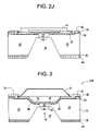
- FIG. 3is a cross sectional view of another embodiment of a backside absolute pressure sensor.
- FIGS. 4( a )- 4 ( h )collectively illustrate an exemplary method of making the embodiment of the backside absolute pressure sensor illustrated in FIG. 3 .
- FIG. 5is an embodiment of a differential pressure sensor.
- a backside microelectromechanical systems (MEMS) based pressure sensor(hereinafter referred to as a pressure sensor) including a first substrate (wafer) and second substrate (wafer), which are silicon fusion bonded together, allows the pressure sensor to be operated in harsh environments (e.g., solvent mixtures (e.g., fuel), water (e.g., salt water), acids, and bases).
- harsh environmentse.g., solvent mixtures (e.g., fuel), water (e.g., salt water), acids, and bases).
- the pressure sensorsare backside pressure sensors, in which piezoresistors (also referred to a piezo-resistive elements) are disposed on, in, or proximate to (hereinafter “on” for convenience in discussion) a side of a diaphragm formed by one of the substrates opposite a side of the diaphragm exposed to the environment.
- the pressure sensorscan be an absolute pressure sensor or a differential pressure sensor.
- the absolute pressure sensor 100includes a base substrate 12 , a cap substrate 14 , and a chamber 16 disposed therebetween.
- the base substrate 12 and the cap substrate 14each include silicon.
- the base substrate 12 and the cap substrate 14each are a multi-layer structure (e.g., a silicon-on-insulator type wafer).
- the base substrate 12 and the cap substrate 14are each a single-layer structure. It is advantageously noted that use of the single-layer structure can reduce the cost of the sensor compared to multi-layer structures.
- the base substrate 12is an n-type substrate.
- the silicon of the base substrate 12is doped with an n-type dopant (e.g., phosphorous).
- the cap substrate 14can be either an n-type substrate or a p-type substrate.
- the cap substrate 14can be doped with a similar or different n-type dopant as that employed in the base substrate 12 .
- the cap substrate 14is doped with a p-type dopant (e.g., boron).
- the base substrate 12includes a cavity 18 , which is defined by walls created in a support portion 20 of the base substrate 12 and defined on a third side by a diaphragm portion 22 of the base substrate 12 . Stated another way, the diaphragm portion is disposed over the cavity 18 . Further, the cavity 18 exposes a first (environmental) side 24 of the diaphragm portion 22 to an environment to be sensed. For example, during operation the environment exerts a pressure, illustrated as line P, against the first side 24 of the diaphragm portion 22 .
- the diaphragm portion 22includes a thickness sufficient to allow the diaphragm to deflect under pressure from the environment.
- Piezo-resistive elements 26are disposed on a second surface 28 of the diaphragm portion 22 .
- the piezo-resistive elements 26are disposed in a region of the diaphragm portion 22 that has the greatest stress during flexure of the diaphragm portion 22 .
- the piezo-resistive elements 26each include a resistance that varies with mechanical stress. The number, type, and arrangement of each piezo-resistive element 26 vary depending on the application. In one embodiment, the piezo-resistive elements 26 are arranged in a Wheatstone bridge circuit.
- the piezo-resistive elements 26measure the flexion of the diaphragm portion 22 due the pressure form the environment.
- Suitable materials for the piezo-resistive elementinclude, but are not limited, to p-type dopants (e.g., boron).
- a conductive pathway 30is disposed in electrical communication with the piezo-resistive elements 26 .
- the conductive pathway 30includes any electrical conductive material.
- the conductive pathway 30can include a portion of the base substrate 12 , which has been doped with a p-type dopant.
- the conductive pathway 30is disposed in electrical communication with an electrode 32 , which is sometimes referred to as a wire bond pad, and the like.
- Suitable materials for the electrode 32include metals (e.g., aluminum, titanium, platinum, gold, and combinations comprising at least one of the foregoing), alloys, and the like.
- the conductive pathway 30is disposed in physical communication with the base portion 12 .
- a first oxide layer 34(e.g., a silicon dioxide layer) is disposed in physical communication with the conductive pathway 30 .
- the first oxide layer 34can be disposed on the conductive pathway 30 and at least a portion of the base substrate 12 (e.g., the second side of the diaphragm portion 22 ). Through holes are disposed in the first oxide layer 34 to allow electrical communication between the electrode 32 and the conductive pathway 30 .
- first nitride layer 36Disposed in physical communication with the first oxide layer 34 is first nitride layer 36 .
- Through holesare disposed in the first nitride layer 36 corresponding to the location of the through holes disposed in the first oxide layer 34 to allow electrical communication between the electrode 32 and the conductive pathway 30 .
- the first oxide layer 34 and the first nitride layer 36each act as insulating layers and/or protective layers for the conductive pathway 30 and the piezo-resistive element 26 .
- the first nitride layer 36includes nitrides, including, but not limited to, silicon nitride.
- a second oxide layer 38 and a second nitride layer 40are respectively disposed on a surface 42 of the base substrate 12 , which is opposite, for example, the second side 28 of the diaphragm portion 22 .
- These layersrespectively include similar materials to those discussed in relation to first oxide layer 24 and first nitride layer 36 .
- the second oxide layer 38 and second nitride layer 40each act as a protective coating during formation of cavity 18 .
- the base substrate 12is silicon fusion bonded to the cap substrate 14 such that a chamber 16 is formed therebetween, which is hermetically sealed from a surrounding environment.
- MIL-STDUnited States military standard
- the base substrate 12 and the cap substrate 14are bonded together in a vacuum such that chamber 16 is a vacuum chamber, which functions as a zero pressure reference when the diaphragm portion 22 is exposed to the environment.
- the chamber 16is formed by a cavity in the cap substrate 14 .
- a cavitycan be disposed in the base substrate 12 to form the chamber 16 .
- the length and width of the cavity forming chamber 16is selected to correspond to at least a length and width of the diaphragm portion 22 .
- the width of the cavitycan be substantially uniform (e.g., the walls are substantially straight) or the walls of the cavity can converge toward the diaphragm portion 22 (e.g. the walls are tapered).
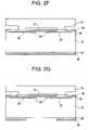
- FIGS. 2( a )-( j )collectively illustrate an exemplary method of making the embodiment of the backside absolute pressure sensor in FIG. 1 .
- the piezo-resistive element 26 and the conductive pathway 30are formed on a surface of the base substrate 12 by, for example, ion implantation, diffusion, and the like. Materials for the piezo-resistive element 26 and conductive pathway 30 include those materials discussed above. FIG.
- FIG. 2( b )illustrates the selective etching away of a portion of the nitride layer 36 to form a bond area (e.g., a bond ring), which is followed by reoxidizing of the base substrate 12 to generate a thicker oxide portion of the first oxidizing layer in the bond area relative to the thickness of the first oxidizing layer 34 prior to etching and oxidizing.
- FIG. 2( c )illustrates the etching away a portion of the nitride layer 36 , while leaving the oxide layer 34 , at a location corresponding to the location of electrodes 32 .
- FIG. 2( d )illustrates the cap substrate 14 including two step heights, which are formed on the cap substrate 14 by, for example, deep reactive ion etching.
- the step heightscorrespond to the desired size of the chamber 16 and are located to correspond to the bond area on the base substrate 12 .
- FIG. 2( e )illustrates the base substrate 12 being silicon fusion bonded to the cap substrate 14 , which is an important feature in making the absolute pressure sensor 100 .
- the base substrate 12 and the cap substrate 14are bonded without any intermediate bond, alloy, adhesive, and the like.
- silicon fusion bondingrefers to the bonding of silicon to silicon or any combination of bonding silicon to a silicon oxide.
- the silicon fusion bondinghas a bond width of about 100 micrometers to about 150 micrometers. The use of silicon fusion bonding allows the pressure sensor 100 to have an active life of at least 10 years, which advantageously allows the absolute pressure sensor 100 to be employed in automotive applications.
- the overall cost of the absolute pressure sensorcan be reduced compared to other devices that employ other bonding technologies.
- a silicon substratewhich is bonded to another silicon substrate using an intermediate layer, has the additional costs associated with the bond material and added processing costs compared to silicon fusion bonding.
- the cost of glass substrates and silicon-on-insulator (SOI) substratesare generally more expensive than the cost of standard silicon substrates. In a competitive market, any reduction in cost, while maintaining or increasing performance, is desirable in gaining market share.
- FIG. 2( f )illustrates the cap substrate 14 being thinned down using grinding and polishing to reduce the overall thickness of the cap substrate 14 .
- the overall thickness of cap substrate 14is up to about 400 micrometers, particularly about 50 micrometers to about 150 micrometers.
- a reduction in materialcorresponds to a reduction in the overall cost of the device.
- a reduction in size in a pressure sensorallows the pressure sensor to be employed in a wider range of applications.
- FIG. 2( g )illustrates a window being formed into the second oxide layer 38 and the second nitride layer 40 by selectively removing a portion of each layer using an etchant similar to the etchant discussed above in relation to the selective removal of first oxide layer 36 .
- the cap layeris formed into a final shape, by for example etching.
- FIG. 2( i )illustrates electrodes 32 being formed by metallization in the area where a window (e.g., a through hole) is formed in each of the first oxide layer 34 and first nitride layer 26 .
- Suitable metallization techniquesinclude, but are not limited to, sputtering and electron beam evaporation deposition.
- FIG. 2( j )illustrates the window formed in the second oxide layer 38 and the second nitride layer 40 being further opened (deepened) by for example, by etching, to form the cavity 18 and the diaphragm portion 22 .
- the cavity 18is formed using an anisotropic etchant.
- Suitable anisotropic etchantsinclude, but are not limited to, potassium hydroxide (KOH), tetramethyl ammonium hydroxide (TMAH), ethylene diamine pyrocatechol (EDP), and the like.
- KOHpotassium hydroxide
- TMAHtetramethyl ammonium hydroxide
- EDPethylene diamine pyrocatechol
- the anisotropic etchingforms the cavity 18 in the base substrate 12 having walls which generally converge from the surface 42 toward the first side 24 of the diaphragm portion 22 formed by the cavity 18 .
- isotropic etchingcan be used to form the cavity 18 .
- Suitable isotropic etchantsinclude
- an embodiment of an absolute pressure sensoris illustrated. While the arrangement of the components of the absolute pressure sensor 200 are substantially the same as the arrangement illustrated by absolute pressure sensor 100 , this embodiment is included herein to highlight that the shape of the chamber 16 and the shape of each substrate (e.g., cap substrate 14 ) can vary. Further, while the chamber 16 is disposed between the base substrate 12 and the cap substrate 14 , the chamber 16 can be formed by a cavity in the base substrate 12 , a cavity in the cap substrate 14 , or a combination of the foregoing. In this example, the shape of the chamber 16 corresponds to the shape of the cap substrate 14 .
- FIGS. 4( a )- 4 ( h )collectively illustrate an exemplary method of making the embodiment of the backside absolute pressure sensor illustrated in FIG. 3 .
- FIG. 4( a )illustrates a window being opened into the first oxide layer 34 , which is further etched as illustrated in FIG. 4( b ).
- an anisotropic etchante.g., KOH, TMAH, EDP, and the like
- KOH, TMAH, EDP, and the likecan be used to form a cavity in the base substrate 12 having tapered walls.
- An oxideis regrown in the etched area as illustrated in FIG. 4( c ).
- FIG. 4( a )- 4 ( h )collectively illustrate an exemplary method of making the embodiment of the backside absolute pressure sensor illustrated in FIG. 3 .
- FIG. 4( a )illustrates a window being opened into the first oxide layer 34 , which is further etched as illustrated in FIG. 4( b ).
- the piezo-resistive element 26 and the conductive pathway 30are formed on a surface of the base substrate 12 by ion implantation, diffusion, and the like. Materials for the piezo-resistive element 26 and conductive pathway 30 include those materials discussed above.
- FIG. 4( e )illustrates the base substrate 12 being silicon fusion bonded to the cap substrate 14 .
- FIG. 4( f )illustrates a silicon nitride being disposed over the first oxide layer 34 and over an outer surface of the cap substrate 14 .
- FIG. 4( g )illustrates electrodes 32 being formed by metallization such that the electrodes electrically communicate with the conductive pathway 30 . Suitable metallization techniques include those metallization techniques discussed above.
- FIG. 4( h )illustrates the second oxide layer 38 and the second nitride layer 40 being etched to form cavity 18 and diaphragm portion 22 .
- the differential pressure sensor 300includes a similar arrangement of components discussed in relation to absolute pressure sensors 100 and 200 , with the exception that the differential pressure 300 further includes a cavity 44 disposed through the cap substrate 14 .
- the cavity 44exposes the chamber 16 to the environment, which allows pressure to act on the diaphragm portion 22 from both the first side 24 and the second side 28 . More particularly, in operation, the diaphragm portion 22 flexes in proportion to the difference in pressure from P and P 2 .
- the piezo-resistive elements 26measure the flexion of the diaphragm portion 22 due that difference in pressure from P and P 2 .
- the absolute pressure sensors 100 and 200can each be made into a differential pressure sensor 300 by etching the cavity 44 into the cap substrate 14 . Suitable etchants include, but are not limited to, KOH and TMAH.
- the resulting differential pressure sensor 300can be fixed to a ceramic substrate by solder bumping and the like.
- a solder bump(shown as an elliptical shape) is disposed in physical communication with electrode 32 and a second electrode, which is disposed on a ceramic substrate.
- the method of forming the differential pressure sensor 300advantageously mitigates debris and the like from being disposed in the cavity 44 , which can potentially build up and block the cavity 44 .
- the absolute pressure sensors disclosed hereininclude a silicon fusion bond between a base substrate and a cap substrate. Further, the absolute pressure sensors are backside absolute pressure sensors.
- the silicon fusion bondprovides a bond strength superior to other bonding techniques (e.g., an intermediate glass frit bond, an adhesive bond, and the like), which allows the pressure sensor to have a useful life of at least 10 years. Further, as briefly mentioned above, silicon fusion bonding also allows the pressure sensor to be constructed at a reduced cost compared to some present day sensors, which can offer a significant commercial advantage.
- the absolute pressure sensorsas a backside pressure sensors, the pressure sensors can advantageously be employed in harsh environments, since the piezo-resistive elements and conductive pathways are shielded from the environment. Again, this construction can increase the useful life of the pressure sensor compared to present day sensors.
Landscapes
- Physics & Mathematics (AREA)
- General Physics & Mathematics (AREA)
- Chemical & Material Sciences (AREA)
- Analytical Chemistry (AREA)
- Engineering & Computer Science (AREA)
- Microelectronics & Electronic Packaging (AREA)
- Measuring Fluid Pressure (AREA)
- Pressure Sensors (AREA)
Abstract
Description
Claims (19)
Priority Applications (7)
| Application Number | Priority Date | Filing Date | Title |
|---|---|---|---|
| US11/210,309US7622782B2 (en) | 2005-08-24 | 2005-08-24 | Pressure sensors and methods of making the same |
| AT06802137TATE532044T1 (en) | 2005-08-24 | 2006-08-22 | PRESSURE SENSORS AND METHOD FOR THE PRODUCTION THEREOF |
| JP2008528091AJP5342236B2 (en) | 2005-08-24 | 2006-08-22 | Pressure sensor and manufacturing method |
| CN2006800310976ACN101248340B (en) | 2005-08-24 | 2006-08-22 | Pressure sensors and methods of making the same |
| EP06802137AEP1920229B1 (en) | 2005-08-24 | 2006-08-22 | Pressure sensors and methods of making the same |
| KR1020087004343AKR101296031B1 (en) | 2005-08-24 | 2006-08-22 | Pressure sensors and methods of making the same |
| PCT/US2006/032858WO2007024911A2 (en) | 2005-08-24 | 2006-08-22 | Pressure sensors and methods of making the same |
Applications Claiming Priority (1)
| Application Number | Priority Date | Filing Date | Title |
|---|---|---|---|
| US11/210,309US7622782B2 (en) | 2005-08-24 | 2005-08-24 | Pressure sensors and methods of making the same |
Publications (2)
| Publication Number | Publication Date |
|---|---|
| US20070052046A1 US20070052046A1 (en) | 2007-03-08 |
| US7622782B2true US7622782B2 (en) | 2009-11-24 |
Family
ID=37487427
Family Applications (1)
| Application Number | Title | Priority Date | Filing Date |
|---|---|---|---|
| US11/210,309Expired - Fee RelatedUS7622782B2 (en) | 2005-08-24 | 2005-08-24 | Pressure sensors and methods of making the same |
Country Status (7)
| Country | Link |
|---|---|
| US (1) | US7622782B2 (en) |
| EP (1) | EP1920229B1 (en) |
| JP (1) | JP5342236B2 (en) |
| KR (1) | KR101296031B1 (en) |
| CN (1) | CN101248340B (en) |
| AT (1) | ATE532044T1 (en) |
| WO (1) | WO2007024911A2 (en) |
Cited By (42)
| Publication number | Priority date | Publication date | Assignee | Title |
|---|---|---|---|---|
| US20070128759A1 (en)* | 2005-12-01 | 2007-06-07 | Dewes Brian E | Plasma discharge method and structure for verifying a hermetical seal |
| US20100031752A1 (en)* | 2006-02-24 | 2010-02-11 | Gilles Delapierre | Pressure sensor with resistance strain gages |
| US20100218613A1 (en)* | 2009-02-27 | 2010-09-02 | Infineon Technologies Ag | Semiconductor device including a cavity |
| US20100258883A1 (en)* | 2009-04-14 | 2010-10-14 | Taiwan Semiconductor Manfacturing Company, Ltd. | Metal-Ceramic Multilayer Structure |
| US20110005326A1 (en)* | 2009-07-10 | 2011-01-13 | Honeywell International Inc. | Sensor package assembly having an unconstrained sense die |
| US20110018075A1 (en)* | 2009-07-23 | 2011-01-27 | Lung-Tai Chen | Structure and fabrication method of a sensing device |
| US20110107839A1 (en)* | 2009-11-11 | 2011-05-12 | Honeywell International Inc. | Pressure sensor assembly |
| US20110121413A1 (en)* | 2009-11-17 | 2011-05-26 | Howard Allen | Microelectromechanical systems microphone packaging systems |
| US7998777B1 (en) | 2010-12-15 | 2011-08-16 | General Electric Company | Method for fabricating a sensor |
| US20110235676A1 (en)* | 2010-03-26 | 2011-09-29 | Seiko Epson Corporation | Thermal detector, thermal detection device, and electronic instrument |
| US8230743B2 (en) | 2010-08-23 | 2012-07-31 | Honeywell International Inc. | Pressure sensor |
| US8710599B2 (en) | 2009-08-04 | 2014-04-29 | Fairchild Semiconductor Corporation | Micromachined devices and fabricating the same |
| US8742964B2 (en) | 2012-04-04 | 2014-06-03 | Fairchild Semiconductor Corporation | Noise reduction method with chopping for a merged MEMS accelerometer sensor |
| US8754694B2 (en) | 2012-04-03 | 2014-06-17 | Fairchild Semiconductor Corporation | Accurate ninety-degree phase shifter |
| US8813564B2 (en) | 2010-09-18 | 2014-08-26 | Fairchild Semiconductor Corporation | MEMS multi-axis gyroscope with central suspension and gimbal structure |
| US20150040675A1 (en)* | 2013-08-09 | 2015-02-12 | Continental Automotive Systems, Inc. | Absolute Pressure Sensor With Improved Bonding Boundary |
| US8978475B2 (en) | 2012-02-01 | 2015-03-17 | Fairchild Semiconductor Corporation | MEMS proof mass with split z-axis portions |
| US9006846B2 (en) | 2010-09-20 | 2015-04-14 | Fairchild Semiconductor Corporation | Through silicon via with reduced shunt capacitance |
| US9010200B2 (en) | 2012-08-06 | 2015-04-21 | Amphenol Thermometrics, Inc. | Device for measuring forces and method of making the same |
| US9062972B2 (en) | 2012-01-31 | 2015-06-23 | Fairchild Semiconductor Corporation | MEMS multi-axis accelerometer electrode structure |
| US9069006B2 (en) | 2012-04-05 | 2015-06-30 | Fairchild Semiconductor Corporation | Self test of MEMS gyroscope with ASICs integrated capacitors |
| US9094027B2 (en) | 2012-04-12 | 2015-07-28 | Fairchild Semiconductor Corporation | Micro-electro-mechanical-system (MEMS) driver |
| US9095072B2 (en) | 2010-09-18 | 2015-07-28 | Fairchild Semiconductor Corporation | Multi-die MEMS package |
| US20150285703A1 (en)* | 2012-10-17 | 2015-10-08 | Kabushiki Kaisha Saginomiya Seisakusho | Pressure sensor, and sensor unit provided with same |
| US9156673B2 (en) | 2010-09-18 | 2015-10-13 | Fairchild Semiconductor Corporation | Packaging to reduce stress on microelectromechanical systems |
| US9246018B2 (en) | 2010-09-18 | 2016-01-26 | Fairchild Semiconductor Corporation | Micromachined monolithic 3-axis gyroscope with single drive |
| US9248205B2 (en) | 2009-09-10 | 2016-02-02 | Syntheon, Llc | Surgical sterilizer with integrated battery charging device |
| US20160033349A1 (en)* | 2014-07-29 | 2016-02-04 | Silicon Microstructures, Inc. | Pressure sensor having cap-defined membrane |
| US9278846B2 (en) | 2010-09-18 | 2016-03-08 | Fairchild Semiconductor Corporation | Micromachined monolithic 6-axis inertial sensor |
| US9352961B2 (en) | 2010-09-18 | 2016-05-31 | Fairchild Semiconductor Corporation | Flexure bearing to reduce quadrature for resonating micromachined devices |
| US20160178467A1 (en)* | 2014-07-29 | 2016-06-23 | Silicon Microstructures, Inc. | Pressure sensor having cap-defined membrane |
| US9425328B2 (en) | 2012-09-12 | 2016-08-23 | Fairchild Semiconductor Corporation | Through silicon via including multi-material fill |
| US20160245709A1 (en)* | 2015-02-19 | 2016-08-25 | Stmicroelectronics S.R.L. | Pressure sensing device with cavity and related methods |
| US9444404B2 (en) | 2012-04-05 | 2016-09-13 | Fairchild Semiconductor Corporation | MEMS device front-end charge amplifier |
| US9488693B2 (en) | 2012-04-04 | 2016-11-08 | Fairchild Semiconductor Corporation | Self test of MEMS accelerometer with ASICS integrated capacitors |
| US20170023426A1 (en)* | 2014-04-04 | 2017-01-26 | Ando Lars Feyh | Membrane-Based Sensor and Method for Robust Manufacture of a Membrane-Based Sensor |
| US9618361B2 (en) | 2012-04-05 | 2017-04-11 | Fairchild Semiconductor Corporation | MEMS device automatic-gain control loop for mechanical amplitude drive |
| US9625272B2 (en) | 2012-04-12 | 2017-04-18 | Fairchild Semiconductor Corporation | MEMS quadrature cancellation and signal demodulation |
| US9835507B2 (en) | 2013-08-06 | 2017-12-05 | Denso Corporation | Dynamic quantity sensor |
| US10060757B2 (en) | 2012-04-05 | 2018-08-28 | Fairchild Semiconductor Corporation | MEMS device quadrature shift cancellation |
| US10065851B2 (en) | 2010-09-20 | 2018-09-04 | Fairchild Semiconductor Corporation | Microelectromechanical pressure sensor including reference capacitor |
| US10809140B2 (en) | 2015-06-22 | 2020-10-20 | Stmicroelectronics S.R.L. | Pressure sensor generating a transduced signal with reduced ambient temperature dependence, and manufacturing method thereof |
Families Citing this family (38)
| Publication number | Priority date | Publication date | Assignee | Title |
|---|---|---|---|---|
| US7304412B2 (en)* | 2005-01-31 | 2007-12-04 | Avago Technologes Wireless Ip (Singapore) Pte Ltd | Apparatus embodying doped substrate portion |
| TWI289879B (en)* | 2005-09-30 | 2007-11-11 | Touch Micro System Tech | Method of fabricating pressure sensor |
| DE102007027274A1 (en)* | 2007-06-11 | 2008-12-18 | Endress + Hauser Gmbh + Co. Kg | Differential Pressure Sensor |
| US7784330B2 (en)* | 2007-10-05 | 2010-08-31 | Schlumberger Technology Corporation | Viscosity measurement |
| TWI364804B (en)* | 2007-11-14 | 2012-05-21 | Ind Tech Res Inst | Wafer level sensor package structure and method therefor |
| JP5001129B2 (en)* | 2007-12-17 | 2012-08-15 | ホーチキ株式会社 | Thermal sensor |
| US8297125B2 (en) | 2008-05-23 | 2012-10-30 | Honeywell International Inc. | Media isolated differential pressure sensor with cap |
| US8230745B2 (en) | 2008-11-19 | 2012-07-31 | Honeywell International Inc. | Wet/wet differential pressure sensor based on microelectronic packaging process |
| DE102008054415A1 (en) | 2008-12-09 | 2010-06-10 | Robert Bosch Gmbh | Arrangement of two substrates with a SLID bond connection and method for producing such an arrangement |
| US7900521B2 (en)* | 2009-02-10 | 2011-03-08 | Freescale Semiconductor, Inc. | Exposed pad backside pressure sensor package |
| US8435821B2 (en)* | 2010-06-18 | 2013-05-07 | General Electric Company | Sensor and method for fabricating the same |
| DE102010063065A1 (en)* | 2010-12-14 | 2012-06-14 | Endress + Hauser Gmbh + Co. Kg | Pressure sensor and method for its manufacture + |
| DE112011104403T5 (en)* | 2010-12-15 | 2013-09-19 | Panasonic Corporation | Semiconductor pressure sensor |
| CN102183335B (en)* | 2011-03-15 | 2015-10-21 | 迈尔森电子(天津)有限公司 | MEMS pressure sensor and preparation method thereof |
| US8993451B2 (en)* | 2011-04-15 | 2015-03-31 | Freescale Semiconductor, Inc. | Etching trenches in a substrate |
| US8709848B2 (en)* | 2011-04-15 | 2014-04-29 | Freescale Semiconductor, Inc. | Method for etched cavity devices |
| US8466523B2 (en)* | 2011-10-07 | 2013-06-18 | Continental Automotive Systems, Inc. | Differential pressure sensor device |
| US9170164B2 (en) | 2012-02-03 | 2015-10-27 | Dieter Naegele-Preissmann | Capacitive pressure sensor and a method of fabricating the same |
| US8833172B2 (en)* | 2012-06-27 | 2014-09-16 | Continental Automotive Systems, Inc | Pressure sensing device with stepped cavity to minimize thermal noise |
| GB2508908B (en)* | 2012-12-14 | 2017-02-15 | Gen Electric | Resonator device |
| CN103964370A (en)* | 2013-01-29 | 2014-08-06 | 北京大学 | Method for preparing capacitive pressure transducer |
| US8878316B2 (en)* | 2013-02-22 | 2014-11-04 | Continental Automotive Systems, Inc. | Cap side bonding structure for backside absolute pressure sensors |
| JP2014169915A (en)* | 2013-03-04 | 2014-09-18 | Denso Corp | Method of manufacturing semiconductor pressure sensor |
| CN103674397B (en)* | 2013-12-03 | 2016-04-20 | 新会康宇测控仪器仪表工程有限公司 | High overload back pressure type absolute pressure sensor module and manufacturing process thereof |
| US9260294B2 (en)* | 2013-12-27 | 2016-02-16 | Intel Corporation | Integration of pressure or inertial sensors into integrated circuit fabrication and packaging |
| CN104296899B (en)* | 2014-09-28 | 2017-04-12 | 缪建民 | High-sensitivity silicon piezoresistance pressure sensor and preparation method thereof |
| CN105527042B (en)* | 2014-10-15 | 2020-06-05 | 浙江盾安人工环境股份有限公司 | Pressure sensor and method for manufacturing the same |
| CN105241369B (en)* | 2015-08-17 | 2018-02-09 | 王文 | MEMS strain gauge chip and manufacturing process thereof |
| JP6555214B2 (en)* | 2016-08-25 | 2019-08-07 | 株式会社デンソー | Pressure sensor |
| US10481025B2 (en)* | 2017-01-26 | 2019-11-19 | Rosemount Aerospace Inc. | Piezoresistive sensor with spring flexures for stress isolation |
| JP6468304B2 (en)* | 2017-02-28 | 2019-02-13 | 株式会社デンソー | Physical quantity sensor |
| KR101985946B1 (en)* | 2018-11-21 | 2019-06-04 | 호산엔지니어링(주) | Load cell device using micro-fused semiconductor gauge |
| CN109682510B (en)* | 2018-12-07 | 2021-05-04 | 中国电子科技集团公司第十三研究所 | GaN high temperature pressure sensor |
| CN109668661B (en)* | 2018-12-07 | 2021-05-04 | 中国电子科技集团公司第十三研究所 | GaN high-temperature pressure sensor |
| CN111337166A (en)* | 2020-03-25 | 2020-06-26 | 电子科技大学 | Preparation method of novel absolute pressure surface acoustic wave pressure sensor |
| AU2022338994A1 (en)* | 2021-08-31 | 2024-02-22 | Huba Control Ag | Metal pressure measuring cell |
| CN114577390A (en)* | 2022-03-03 | 2022-06-03 | 苏州跃芯微传感技术有限公司 | Low-voltage MEMS pressure sensor and preparation method thereof |
| CN118168706A (en)* | 2024-03-13 | 2024-06-11 | 京东方科技集团股份有限公司 | Pressure sensor, method for manufacturing pressure sensor, air conditioning device and vehicle |
Citations (23)
| Publication number | Priority date | Publication date | Assignee | Title |
|---|---|---|---|---|
| US4291293A (en) | 1978-09-27 | 1981-09-22 | Hitachi, Ltd. | Semiconductor absolute pressure transducer assembly and method |
| US4525766A (en) | 1984-01-25 | 1985-06-25 | Transensory Devices, Inc. | Method and apparatus for forming hermetically sealed electrical feedthrough conductors |
| US4800758A (en)* | 1986-06-23 | 1989-01-31 | Rosemount Inc. | Pressure transducer with stress isolation for hard mounting |
| US4802952A (en) | 1987-03-06 | 1989-02-07 | Hitachi, Ltd. | Method for manufacturing semiconductor absolute pressure sensor units |
| US5095349A (en)* | 1988-06-08 | 1992-03-10 | Nippondenso Co., Ltd. | Semiconductor pressure sensor and method of manufacturing same |
| US5157973A (en) | 1989-03-16 | 1992-10-27 | Process Automation Business, Inc. | Pressure sensor with integral overpressure protection |
| US5231301A (en) | 1991-10-02 | 1993-07-27 | Lucas Novasensor | Semiconductor sensor with piezoresistors and improved electrostatic structures |
| US5273205A (en) | 1991-11-21 | 1993-12-28 | Korea Institute Of Science And Technology | Method and apparatus for silicon fusion bonding of silicon substrates using wet oxygen atmosphere |
| US5591679A (en) | 1995-04-12 | 1997-01-07 | Sensonor A/S | Sealed cavity arrangement method |
| US5600071A (en) | 1995-09-05 | 1997-02-04 | Motorola, Inc. | Vertically integrated sensor structure and method |
| JPH10325772A (en)* | 1997-05-27 | 1998-12-08 | Nissan Motor Co Ltd | Semiconductor pressure sensor and method of manufacturing the same |
| WO2000002028A1 (en) | 1998-07-07 | 2000-01-13 | The Goodyear Tire & Rubber Company | Method of fabricating silicon capacitive sensor |
| US6038928A (en) | 1996-10-07 | 2000-03-21 | Lucas Novasensor | Miniature gauge pressure sensor using silicon fusion bonding and back etching |
| US6074891A (en) | 1998-06-16 | 2000-06-13 | Delphi Technologies, Inc. | Process for verifying a hermetic seal and semiconductor device therefor |
| US6406636B1 (en) | 1999-06-02 | 2002-06-18 | Megasense, Inc. | Methods for wafer to wafer bonding using microstructures |
| US6472244B1 (en) | 1996-07-31 | 2002-10-29 | Sgs-Thomson Microelectronics S.R.L. | Manufacturing method and integrated microstructures of semiconductor material and integrated piezoresistive pressure sensor having a diaphragm of polycrystalline semiconductor material |
| US20030019299A1 (en)* | 1998-03-31 | 2003-01-30 | Hitachi, Ltd. | Capacitive type pressure sensor |
| EP1359402A1 (en) | 2002-05-01 | 2003-11-05 | SensoNor asa | Pressure sensor |
| US6647794B1 (en)* | 2002-05-06 | 2003-11-18 | Rosemount Inc. | Absolute pressure sensor |
| WO2004050546A2 (en) | 2002-12-05 | 2004-06-17 | X-Fab Semiconductor Foundries Ag | System for sensorless control in a permanent magnet machine |
| US20050037534A1 (en) | 2001-01-02 | 2005-02-17 | Sawyer William D. | MEMS device and interposer and method for integrating MEMS device and interposer |
| EP1522521A1 (en) | 2003-10-10 | 2005-04-13 | SensoNor asa | Capacitive sensor |
| US7197939B2 (en)* | 2004-02-09 | 2007-04-03 | Denso Corporation | Pressure sensor |
Family Cites Families (7)
| Publication number | Priority date | Publication date | Assignee | Title |
|---|---|---|---|---|
| JPH07110277A (en)* | 1993-10-08 | 1995-04-25 | Oki Electric Ind Co Ltd | Silicon pressure sensor |
| JP3401992B2 (en)* | 1995-05-17 | 2003-04-28 | 株式会社デンソー | Semiconductor strain sensor |
| JPH11311579A (en)* | 1998-04-28 | 1999-11-09 | Matsushita Electric Works Ltd | Method for forming diaphragm of semiconductor pressure sensor |
| JP3545224B2 (en)* | 1998-10-06 | 2004-07-21 | 株式会社日立ユニシアオートモティブ | Pressure sensor |
| JP2002039892A (en)* | 2000-07-28 | 2002-02-06 | Matsushita Electric Works Ltd | Semiconductor pressure sensor and method of manufacturing it |
| JP2005043159A (en)* | 2003-07-25 | 2005-02-17 | Hitachi Unisia Automotive Ltd | Pressure sensor |
| JP4314977B2 (en) | 2003-11-20 | 2009-08-19 | パナソニック電工株式会社 | Pressure sensor and method for manufacturing the pressure sensor |
- 2005
- 2005-08-24USUS11/210,309patent/US7622782B2/ennot_activeExpired - Fee Related
- 2006
- 2006-08-22EPEP06802137Apatent/EP1920229B1/ennot_activeNot-in-force
- 2006-08-22JPJP2008528091Apatent/JP5342236B2/ennot_activeExpired - Fee Related
- 2006-08-22WOPCT/US2006/032858patent/WO2007024911A2/enactiveApplication Filing
- 2006-08-22CNCN2006800310976Apatent/CN101248340B/ennot_activeExpired - Fee Related
- 2006-08-22KRKR1020087004343Apatent/KR101296031B1/ennot_activeExpired - Fee Related
- 2006-08-22ATAT06802137Tpatent/ATE532044T1/enactive
Patent Citations (24)
| Publication number | Priority date | Publication date | Assignee | Title |
|---|---|---|---|---|
| US4291293A (en) | 1978-09-27 | 1981-09-22 | Hitachi, Ltd. | Semiconductor absolute pressure transducer assembly and method |
| US4525766A (en) | 1984-01-25 | 1985-06-25 | Transensory Devices, Inc. | Method and apparatus for forming hermetically sealed electrical feedthrough conductors |
| US4800758A (en)* | 1986-06-23 | 1989-01-31 | Rosemount Inc. | Pressure transducer with stress isolation for hard mounting |
| US4802952A (en) | 1987-03-06 | 1989-02-07 | Hitachi, Ltd. | Method for manufacturing semiconductor absolute pressure sensor units |
| US5095349A (en)* | 1988-06-08 | 1992-03-10 | Nippondenso Co., Ltd. | Semiconductor pressure sensor and method of manufacturing same |
| US5157973A (en) | 1989-03-16 | 1992-10-27 | Process Automation Business, Inc. | Pressure sensor with integral overpressure protection |
| US5231301A (en) | 1991-10-02 | 1993-07-27 | Lucas Novasensor | Semiconductor sensor with piezoresistors and improved electrostatic structures |
| US5273205A (en) | 1991-11-21 | 1993-12-28 | Korea Institute Of Science And Technology | Method and apparatus for silicon fusion bonding of silicon substrates using wet oxygen atmosphere |
| US5591679A (en) | 1995-04-12 | 1997-01-07 | Sensonor A/S | Sealed cavity arrangement method |
| US5600071A (en) | 1995-09-05 | 1997-02-04 | Motorola, Inc. | Vertically integrated sensor structure and method |
| US6472244B1 (en) | 1996-07-31 | 2002-10-29 | Sgs-Thomson Microelectronics S.R.L. | Manufacturing method and integrated microstructures of semiconductor material and integrated piezoresistive pressure sensor having a diaphragm of polycrystalline semiconductor material |
| US6038928A (en) | 1996-10-07 | 2000-03-21 | Lucas Novasensor | Miniature gauge pressure sensor using silicon fusion bonding and back etching |
| US6629465B1 (en) | 1996-10-07 | 2003-10-07 | Novasensor Inc. | Miniature gauge pressure sensor using silicon fusion bonding and back etching |
| JPH10325772A (en)* | 1997-05-27 | 1998-12-08 | Nissan Motor Co Ltd | Semiconductor pressure sensor and method of manufacturing the same |
| US20030019299A1 (en)* | 1998-03-31 | 2003-01-30 | Hitachi, Ltd. | Capacitive type pressure sensor |
| US6074891A (en) | 1998-06-16 | 2000-06-13 | Delphi Technologies, Inc. | Process for verifying a hermetic seal and semiconductor device therefor |
| WO2000002028A1 (en) | 1998-07-07 | 2000-01-13 | The Goodyear Tire & Rubber Company | Method of fabricating silicon capacitive sensor |
| US6406636B1 (en) | 1999-06-02 | 2002-06-18 | Megasense, Inc. | Methods for wafer to wafer bonding using microstructures |
| US20050037534A1 (en) | 2001-01-02 | 2005-02-17 | Sawyer William D. | MEMS device and interposer and method for integrating MEMS device and interposer |
| EP1359402A1 (en) | 2002-05-01 | 2003-11-05 | SensoNor asa | Pressure sensor |
| US6647794B1 (en)* | 2002-05-06 | 2003-11-18 | Rosemount Inc. | Absolute pressure sensor |
| WO2004050546A2 (en) | 2002-12-05 | 2004-06-17 | X-Fab Semiconductor Foundries Ag | System for sensorless control in a permanent magnet machine |
| EP1522521A1 (en) | 2003-10-10 | 2005-04-13 | SensoNor asa | Capacitive sensor |
| US7197939B2 (en)* | 2004-02-09 | 2007-04-03 | Denso Corporation | Pressure sensor |
Non-Patent Citations (3)
| Title |
|---|
| High Pressure Sensor Based on Fusion Bonding, Birkelund et al., presented at 2001 Joint International Meeting of The Electromechanical Society, Inc. and International Society of Electrochemistry in San Francisco, CA on Sep. 2-7, 2001. |
| International Search Report; PCT/US2006/032858 with an International Filing Date of Aug. 22, 2006. |
| MIL-STD-883E, dated Mar. 14, 1995. |
Cited By (65)
| Publication number | Priority date | Publication date | Assignee | Title |
|---|---|---|---|---|
| US20070128759A1 (en)* | 2005-12-01 | 2007-06-07 | Dewes Brian E | Plasma discharge method and structure for verifying a hermetical seal |
| US7880113B2 (en)* | 2005-12-01 | 2011-02-01 | Delphi Technologies, Inc. | Plasma discharge method and structure for verifying a hermetical seal |
| US20100031752A1 (en)* | 2006-02-24 | 2010-02-11 | Gilles Delapierre | Pressure sensor with resistance strain gages |
| US8393223B2 (en)* | 2006-02-24 | 2013-03-12 | Commissariat A L'energie Atomique | Pressure sensor with resistance strain gages |
| US20100218613A1 (en)* | 2009-02-27 | 2010-09-02 | Infineon Technologies Ag | Semiconductor device including a cavity |
| US8471346B2 (en)* | 2009-02-27 | 2013-06-25 | Infineon Technologies Ag | Semiconductor device including a cavity |
| US8237235B2 (en)* | 2009-04-14 | 2012-08-07 | Taiwan Semiconductor Manufacturing Company, Ltd. | Metal-ceramic multilayer structure |
| US20100258883A1 (en)* | 2009-04-14 | 2010-10-14 | Taiwan Semiconductor Manfacturing Company, Ltd. | Metal-Ceramic Multilayer Structure |
| US20110005326A1 (en)* | 2009-07-10 | 2011-01-13 | Honeywell International Inc. | Sensor package assembly having an unconstrained sense die |
| US8322225B2 (en) | 2009-07-10 | 2012-12-04 | Honeywell International Inc. | Sensor package assembly having an unconstrained sense die |
| US20110018075A1 (en)* | 2009-07-23 | 2011-01-27 | Lung-Tai Chen | Structure and fabrication method of a sensing device |
| US9133018B2 (en)* | 2009-07-23 | 2015-09-15 | Industrial Technology Research Institute | Structure and fabrication method of a sensing device |
| US8710599B2 (en) | 2009-08-04 | 2014-04-29 | Fairchild Semiconductor Corporation | Micromachined devices and fabricating the same |
| US8739626B2 (en) | 2009-08-04 | 2014-06-03 | Fairchild Semiconductor Corporation | Micromachined inertial sensor devices |
| US9248205B2 (en) | 2009-09-10 | 2016-02-02 | Syntheon, Llc | Surgical sterilizer with integrated battery charging device |
| US8082797B2 (en) | 2009-11-11 | 2011-12-27 | Honeywell International Inc. | Pressure sensor assembly |
| US20110107839A1 (en)* | 2009-11-11 | 2011-05-12 | Honeywell International Inc. | Pressure sensor assembly |
| US8567254B2 (en) | 2009-11-11 | 2013-10-29 | Honeywell International Inc. | Pressure sensor assembly |
| US20110121413A1 (en)* | 2009-11-17 | 2011-05-26 | Howard Allen | Microelectromechanical systems microphone packaging systems |
| US8421168B2 (en) | 2009-11-17 | 2013-04-16 | Fairchild Semiconductor Corporation | Microelectromechanical systems microphone packaging systems |
| US20110235676A1 (en)* | 2010-03-26 | 2011-09-29 | Seiko Epson Corporation | Thermal detector, thermal detection device, and electronic instrument |
| US9182288B2 (en)* | 2010-03-26 | 2015-11-10 | Seiko Epson Corporation | Thermal detector, thermal detection device, and electronic instrument |
| US8230743B2 (en) | 2010-08-23 | 2012-07-31 | Honeywell International Inc. | Pressure sensor |
| US9095072B2 (en) | 2010-09-18 | 2015-07-28 | Fairchild Semiconductor Corporation | Multi-die MEMS package |
| US9278845B2 (en) | 2010-09-18 | 2016-03-08 | Fairchild Semiconductor Corporation | MEMS multi-axis gyroscope Z-axis electrode structure |
| US10050155B2 (en) | 2010-09-18 | 2018-08-14 | Fairchild Semiconductor Corporation | Micromachined monolithic 3-axis gyroscope with single drive |
| US9246018B2 (en) | 2010-09-18 | 2016-01-26 | Fairchild Semiconductor Corporation | Micromachined monolithic 3-axis gyroscope with single drive |
| US9352961B2 (en) | 2010-09-18 | 2016-05-31 | Fairchild Semiconductor Corporation | Flexure bearing to reduce quadrature for resonating micromachined devices |
| US9856132B2 (en) | 2010-09-18 | 2018-01-02 | Fairchild Semiconductor Corporation | Sealed packaging for microelectromechanical systems |
| US9586813B2 (en) | 2010-09-18 | 2017-03-07 | Fairchild Semiconductor Corporation | Multi-die MEMS package |
| US9455354B2 (en) | 2010-09-18 | 2016-09-27 | Fairchild Semiconductor Corporation | Micromachined 3-axis accelerometer with a single proof-mass |
| US8813564B2 (en) | 2010-09-18 | 2014-08-26 | Fairchild Semiconductor Corporation | MEMS multi-axis gyroscope with central suspension and gimbal structure |
| US9278846B2 (en) | 2010-09-18 | 2016-03-08 | Fairchild Semiconductor Corporation | Micromachined monolithic 6-axis inertial sensor |
| US9156673B2 (en) | 2010-09-18 | 2015-10-13 | Fairchild Semiconductor Corporation | Packaging to reduce stress on microelectromechanical systems |
| US10065851B2 (en) | 2010-09-20 | 2018-09-04 | Fairchild Semiconductor Corporation | Microelectromechanical pressure sensor including reference capacitor |
| US9006846B2 (en) | 2010-09-20 | 2015-04-14 | Fairchild Semiconductor Corporation | Through silicon via with reduced shunt capacitance |
| US7998777B1 (en) | 2010-12-15 | 2011-08-16 | General Electric Company | Method for fabricating a sensor |
| US9062972B2 (en) | 2012-01-31 | 2015-06-23 | Fairchild Semiconductor Corporation | MEMS multi-axis accelerometer electrode structure |
| US9599472B2 (en) | 2012-02-01 | 2017-03-21 | Fairchild Semiconductor Corporation | MEMS proof mass with split Z-axis portions |
| US8978475B2 (en) | 2012-02-01 | 2015-03-17 | Fairchild Semiconductor Corporation | MEMS proof mass with split z-axis portions |
| US8754694B2 (en) | 2012-04-03 | 2014-06-17 | Fairchild Semiconductor Corporation | Accurate ninety-degree phase shifter |
| US8742964B2 (en) | 2012-04-04 | 2014-06-03 | Fairchild Semiconductor Corporation | Noise reduction method with chopping for a merged MEMS accelerometer sensor |
| US9488693B2 (en) | 2012-04-04 | 2016-11-08 | Fairchild Semiconductor Corporation | Self test of MEMS accelerometer with ASICS integrated capacitors |
| US10060757B2 (en) | 2012-04-05 | 2018-08-28 | Fairchild Semiconductor Corporation | MEMS device quadrature shift cancellation |
| US9444404B2 (en) | 2012-04-05 | 2016-09-13 | Fairchild Semiconductor Corporation | MEMS device front-end charge amplifier |
| US9618361B2 (en) | 2012-04-05 | 2017-04-11 | Fairchild Semiconductor Corporation | MEMS device automatic-gain control loop for mechanical amplitude drive |
| US9069006B2 (en) | 2012-04-05 | 2015-06-30 | Fairchild Semiconductor Corporation | Self test of MEMS gyroscope with ASICs integrated capacitors |
| US9094027B2 (en) | 2012-04-12 | 2015-07-28 | Fairchild Semiconductor Corporation | Micro-electro-mechanical-system (MEMS) driver |
| US9625272B2 (en) | 2012-04-12 | 2017-04-18 | Fairchild Semiconductor Corporation | MEMS quadrature cancellation and signal demodulation |
| US9010200B2 (en) | 2012-08-06 | 2015-04-21 | Amphenol Thermometrics, Inc. | Device for measuring forces and method of making the same |
| US9425328B2 (en) | 2012-09-12 | 2016-08-23 | Fairchild Semiconductor Corporation | Through silicon via including multi-material fill |
| US9802814B2 (en) | 2012-09-12 | 2017-10-31 | Fairchild Semiconductor Corporation | Through silicon via including multi-material fill |
| US9733142B2 (en)* | 2012-10-17 | 2017-08-15 | Kabushiki Kaisha Saginomiya Seisakusho | Pressure sensor, and sensor unit provided with same |
| US20150285703A1 (en)* | 2012-10-17 | 2015-10-08 | Kabushiki Kaisha Saginomiya Seisakusho | Pressure sensor, and sensor unit provided with same |
| US9835507B2 (en) | 2013-08-06 | 2017-12-05 | Denso Corporation | Dynamic quantity sensor |
| US20150040675A1 (en)* | 2013-08-09 | 2015-02-12 | Continental Automotive Systems, Inc. | Absolute Pressure Sensor With Improved Bonding Boundary |
| US9546922B2 (en)* | 2013-08-09 | 2017-01-17 | Continental Automotive Systems, Inc. | Absolute pressure sensor with improved cap bonding boundary |
| US20170023426A1 (en)* | 2014-04-04 | 2017-01-26 | Ando Lars Feyh | Membrane-Based Sensor and Method for Robust Manufacture of a Membrane-Based Sensor |
| US11402288B2 (en)* | 2014-04-04 | 2022-08-02 | Robert Bosch Gmbh | Membrane-based sensor having a plurality of spacers extending from a cap layer |
| US20160178467A1 (en)* | 2014-07-29 | 2016-06-23 | Silicon Microstructures, Inc. | Pressure sensor having cap-defined membrane |
| US20160033349A1 (en)* | 2014-07-29 | 2016-02-04 | Silicon Microstructures, Inc. | Pressure sensor having cap-defined membrane |
| US20160245709A1 (en)* | 2015-02-19 | 2016-08-25 | Stmicroelectronics S.R.L. | Pressure sensing device with cavity and related methods |
| US9939338B2 (en)* | 2015-02-19 | 2018-04-10 | Stmicroelectronics S.R.L. | Pressure sensing device with cavity and related methods |
| US10809140B2 (en) | 2015-06-22 | 2020-10-20 | Stmicroelectronics S.R.L. | Pressure sensor generating a transduced signal with reduced ambient temperature dependence, and manufacturing method thereof |
| US10962431B2 (en) | 2015-06-22 | 2021-03-30 | Stmicroelectronics S.R.L. | Pressure sensor generating a transduced signal with reduced ambient temperature dependence, and manufacturing method thereof |
Also Published As
| Publication number | Publication date |
|---|---|
| WO2007024911A3 (en) | 2007-06-14 |
| JP5342236B2 (en) | 2013-11-13 |
| JP2009506323A (en) | 2009-02-12 |
| KR101296031B1 (en) | 2013-08-12 |
| WO2007024911A2 (en) | 2007-03-01 |
| EP1920229B1 (en) | 2011-11-02 |
| KR20080031969A (en) | 2008-04-11 |
| US20070052046A1 (en) | 2007-03-08 |
| EP1920229A2 (en) | 2008-05-14 |
| CN101248340B (en) | 2012-11-14 |
| ATE532044T1 (en) | 2011-11-15 |
| CN101248340A (en) | 2008-08-20 |
Similar Documents
| Publication | Publication Date | Title |
|---|---|---|
| US7622782B2 (en) | Pressure sensors and methods of making the same | |
| US9581512B2 (en) | Pressure sensor with deformable membrane and method of manufacture | |
| EP1860417B1 (en) | A pressure sensor having a chamber and a method for fabricating the same | |
| US7998777B1 (en) | Method for fabricating a sensor | |
| EP1860418A1 (en) | A method for fabricating a pressure sensor using SOI wafers | |
| US20140268523A1 (en) | Wearable device having a monolithically integrated multi-sensor device on a semiconductor substrate and method therefor | |
| US7997142B2 (en) | Low pressure sensor device with high accuracy and high sensitivity | |
| EP3052901B1 (en) | Inertial and pressure sensors on single chip | |
| KR102161035B1 (en) | Sensor device and manufacturing method thereof | |
| WO2010049794A1 (en) | Pressure sensor and wire guide assembly | |
| JP2015515609A (en) | Catheter die and manufacturing method thereof | |
| EP2873958B1 (en) | Capacitive pressure sensors for high temperature applications | |
| EP2182340A1 (en) | Pressure Sensor and Guide Wire Assembly | |
| JP3173256B2 (en) | Semiconductor acceleration sensor and method of manufacturing the same | |
| JPH075192A (en) | Semiconductor acceleration sensor and manufacturing method thereof | |
| US8387459B2 (en) | MEMS sensor | |
| JP2003004566A (en) | Capacitive pressure sensor and method of manufacturing the same |
Legal Events
| Date | Code | Title | Description |
|---|---|---|---|
| AS | Assignment | Owner name:GENERAL ELECTRIC COMPANY, NEW YORK Free format text:ASSIGNMENT OF ASSIGNORS INTEREST;ASSIGNORS:CHU, STANLEY;GAMAGE, SISIRA KANKANAM;KWON, HYON-JIN;REEL/FRAME:016911/0524 Effective date:20050822 | |
| FEPP | Fee payment procedure | Free format text:PAYOR NUMBER ASSIGNED (ORIGINAL EVENT CODE: ASPN); ENTITY STATUS OF PATENT OWNER: LARGE ENTITY | |
| FPAY | Fee payment | Year of fee payment:4 | |
| AS | Assignment | Owner name:AMPHENOL CORPORATION, CONNECTICUT Free format text:ASSIGNMENT OF ASSIGNORS INTEREST;ASSIGNOR:GENERAL ELECTRIC COMPANY;REEL/FRAME:032679/0265 Effective date:20131218 | |
| AS | Assignment | Owner name:GE THERMOMETRICS, INC., PENNSYLVANIA Free format text:ASSIGNMENT OF ASSIGNORS INTEREST;ASSIGNOR:AMPHENOL CORPORATION;REEL/FRAME:032745/0924 Effective date:20131218 | |
| AS | Assignment | Owner name:AMPHENOL THERMOMETRICS, INC., PENNSYLVANIA Free format text:CHANGE OF NAME;ASSIGNOR:GE THERMOMETRICS, INC.;REEL/FRAME:032763/0141 Effective date:20131219 | |
| REMI | Maintenance fee reminder mailed | ||
| LAPS | Lapse for failure to pay maintenance fees | Free format text:PATENT EXPIRED FOR FAILURE TO PAY MAINTENANCE FEES (ORIGINAL EVENT CODE: EXP.) | |
| STCH | Information on status: patent discontinuation | Free format text:PATENT EXPIRED DUE TO NONPAYMENT OF MAINTENANCE FEES UNDER 37 CFR 1.362 | |
| FP | Lapsed due to failure to pay maintenance fee | Effective date:20171124 |