US7621781B2 - Electrical connector with crosstalk canceling features - Google Patents
Electrical connector with crosstalk canceling featuresDownload PDFInfo
- Publication number
- US7621781B2 US7621781B2US11/726,346US72634607AUS7621781B2US 7621781 B2US7621781 B2US 7621781B2US 72634607 AUS72634607 AUS 72634607AUS 7621781 B2US7621781 B2US 7621781B2
- Authority
- US
- United States
- Prior art keywords
- signal
- contacts
- connector
- contact
- offset
- Prior art date
- Legal status (The legal status is an assumption and is not a legal conclusion. Google has not performed a legal analysis and makes no representation as to the accuracy of the status listed.)
- Active
Links
Images


Classifications
- H—ELECTRICITY
- H01—ELECTRIC ELEMENTS
- H01R—ELECTRICALLY-CONDUCTIVE CONNECTIONS; STRUCTURAL ASSOCIATIONS OF A PLURALITY OF MUTUALLY-INSULATED ELECTRICAL CONNECTING ELEMENTS; COUPLING DEVICES; CURRENT COLLECTORS
- H01R13/00—Details of coupling devices of the kinds covered by groups H01R12/70 or H01R24/00 - H01R33/00
- H01R13/02—Contact members
- H01R13/04—Pins or blades for co-operation with sockets
- H—ELECTRICITY
- H01—ELECTRIC ELEMENTS
- H01R—ELECTRICALLY-CONDUCTIVE CONNECTIONS; STRUCTURAL ASSOCIATIONS OF A PLURALITY OF MUTUALLY-INSULATED ELECTRICAL CONNECTING ELEMENTS; COUPLING DEVICES; CURRENT COLLECTORS
- H01R13/00—Details of coupling devices of the kinds covered by groups H01R12/70 or H01R24/00 - H01R33/00
- H01R13/646—Details of coupling devices of the kinds covered by groups H01R12/70 or H01R24/00 - H01R33/00 specially adapted for high-frequency, e.g. structures providing an impedance match or phase match
- H01R13/6461—Means for preventing cross-talk
- H01R13/6467—Means for preventing cross-talk by cross-over of signal conductors
- H—ELECTRICITY
- H01—ELECTRIC ELEMENTS
- H01R—ELECTRICALLY-CONDUCTIVE CONNECTIONS; STRUCTURAL ASSOCIATIONS OF A PLURALITY OF MUTUALLY-INSULATED ELECTRICAL CONNECTING ELEMENTS; COUPLING DEVICES; CURRENT COLLECTORS
- H01R13/00—Details of coupling devices of the kinds covered by groups H01R12/70 or H01R24/00 - H01R33/00
- H01R13/646—Details of coupling devices of the kinds covered by groups H01R12/70 or H01R24/00 - H01R33/00 specially adapted for high-frequency, e.g. structures providing an impedance match or phase match
- H01R13/6461—Means for preventing cross-talk
- H01R13/6471—Means for preventing cross-talk by special arrangement of ground and signal conductors, e.g. GSGS [Ground-Signal-Ground-Signal]
- H—ELECTRICITY
- H01—ELECTRIC ELEMENTS
- H01R—ELECTRICALLY-CONDUCTIVE CONNECTIONS; STRUCTURAL ASSOCIATIONS OF A PLURALITY OF MUTUALLY-INSULATED ELECTRICAL CONNECTING ELEMENTS; COUPLING DEVICES; CURRENT COLLECTORS
- H01R13/00—Details of coupling devices of the kinds covered by groups H01R12/70 or H01R24/00 - H01R33/00
- H01R13/648—Protective earth or shield arrangements on coupling devices, e.g. anti-static shielding
- H01R13/658—High frequency shielding arrangements, e.g. against EMI [Electro-Magnetic Interference] or EMP [Electro-Magnetic Pulse]
- H01R13/6581—Shield structure
- H01R13/6585—Shielding material individually surrounding or interposed between mutually spaced contacts
- H—ELECTRICITY
- H01—ELECTRIC ELEMENTS
- H01R—ELECTRICALLY-CONDUCTIVE CONNECTIONS; STRUCTURAL ASSOCIATIONS OF A PLURALITY OF MUTUALLY-INSULATED ELECTRICAL CONNECTING ELEMENTS; COUPLING DEVICES; CURRENT COLLECTORS
- H01R12/00—Structural associations of a plurality of mutually-insulated electrical connecting elements, specially adapted for printed circuits, e.g. printed circuit boards [PCB], flat or ribbon cables, or like generally planar structures, e.g. terminal strips, terminal blocks; Coupling devices specially adapted for printed circuits, flat or ribbon cables, or like generally planar structures; Terminals specially adapted for contact with, or insertion into, printed circuits, flat or ribbon cables, or like generally planar structures
- H01R12/70—Coupling devices
- H01R12/71—Coupling devices for rigid printing circuits or like structures
- H01R12/72—Coupling devices for rigid printing circuits or like structures coupling with the edge of the rigid printed circuits or like structures
- H01R12/722—Coupling devices for rigid printing circuits or like structures coupling with the edge of the rigid printed circuits or like structures coupling devices mounted on the edge of the printed circuits
- H01R12/724—Coupling devices for rigid printing circuits or like structures coupling with the edge of the rigid printed circuits or like structures coupling devices mounted on the edge of the printed circuits containing contact members forming a right angle
- Y—GENERAL TAGGING OF NEW TECHNOLOGICAL DEVELOPMENTS; GENERAL TAGGING OF CROSS-SECTIONAL TECHNOLOGIES SPANNING OVER SEVERAL SECTIONS OF THE IPC; TECHNICAL SUBJECTS COVERED BY FORMER USPC CROSS-REFERENCE ART COLLECTIONS [XRACs] AND DIGESTS
- Y10—TECHNICAL SUBJECTS COVERED BY FORMER USPC
- Y10S—TECHNICAL SUBJECTS COVERED BY FORMER USPC CROSS-REFERENCE ART COLLECTIONS [XRACs] AND DIGESTS
- Y10S439/00—Electrical connectors
- Y10S439/941—Crosstalk suppression
Definitions
- the inventionrelates generally to electrical connectors and, more particularly, to far end crosstalk reduction in electrical connectors.
- Some electrical systemssuch as network switches or a computer server with switching capability, include large backplanes with several switch cards and line cards plugged into the backplane. When cards are plugged into both sides of a circuit board, the circuit board is called a midplane. Generally, the line cards bring data from external sources into the system. The switch cards contain circuitry that may switch data from one line card to another. Traces in the backplane interconnect the line cards and the appropriate switch cards.
- Some signal lossis inherent in a trace through printed circuit board material. As the number of card connections increases, more traces are required in the backplane. The increased number of traces and the length of the traces in the backplane introduce more and more signal loss in the backplane, particularly at higher signal speeds. Signal loss problems may be addressed by keeping traces in the backplane as short as possible. Connectors are sometimes oriented orthogonally on both sides of a midplane. With orthogonal connectors, the number and lengths of traces in the midplane may be reduced, thereby reducing trace losses in the midplane. Moreover, when connectors connect directly through the midplane, there are no traces.
- crosstalktypically, some amount of crosstalk is present in electrical connectors, including orthogonal connectors.
- a connectorsuch as a connector carrying multiple pairs of differential signals
- crosstalk couplingmay occur in adjacent signal lines. If the coupled energy is sufficient, bit errors may be generated in an adjacent signal line.
- Crosstalkpropagates in both directions in the adjacent lines.
- Near end crosstalkrefers to crosstalk that propagates in the direction opposite to that of the aggressor signal, or the signal generating the crosstalk.
- Far end crosstalkrefers to crosstalk that propagates in the same direction as the aggressor signal.
- Far end crosstalkis additive. That is, far end noise builds upon itself, or is cumulative. In some applications, because of its additive quality, far end crosstalk tends to be the most troublesome.
- an electrical connector systemin one aspect, includes first and second connector assemblies.
- Each connector assemblyincludes contacts arranged in at least two differential pairs wherein one of the pairs is an aggressor pair and one of the pairs is a victim pair.
- a differential signal carried by the aggressor pairgenerates far end crosstalk on the victim pair.
- the contactsare arranged such that, when the first and second connector assemblies are electrically connected to each other, the far end crosstalk on the victim pair in the first connector assembly has a magnitude and a polarity, and the far end crosstalk on the victim pair in the second connector assembly has the same magnitude and an opposite polarity.
- the contactsinclude mating ends and mounting ends and each of the differential contact pairs is arranged along a centerline of a contact row.
- One of the differential contact paircomprises straight contacts and the other of the differential contact pair comprises offset contacts.
- the mounting ends of the offset contact pairare offset on opposite sides of the centerline of the row that includes the offset contact pair.
- Each offset contactincludes a mid-section formed with the mating end.
- the mating end and the mid-sectionlie in a plane.
- The, offset contactincludes a plate that extends from the mid-section at an angle of about forty-five degrees with respect to the plane.
- the housingincludes a base having signal contact cavities. At least one of the signal contact cavities including a slot configured to receive the plate to orient the offset contact in the signal contact cavity.
- an electrical connectorin another aspect, includes a housing having a mating face and a mounting face.
- the housingholds signal contacts and ground contacts arranged in rows.
- Each of the signal contacts and ground contactsincludes a mating end extending from the mating face of the housing and a mounting end extending from the mounting face of the housing.
- the signal contactsare arranged in alternating pairs of straight signal contacts and offset signal contacts, and wherein for each said row, said mounting ends of the ground contacts and the straight signal contacts are arranged along a centerline of the row and the mating ends of the offset signal contacts in each pair of offset signal contacts are offset on opposite sides of the centerline.
- an orthogonal connector assemblyin yet another aspect, includes a pair of connectors configured to be electrically connected to one another from opposite sides of a circuit board.
- the orthogonal connector assemblyincludes first and second connector housings, each having a mating face and a mounting face.
- the mounting facesare configured to be electrically connected to one another from opposite sides of the circuit board in line with one another along a longitudinal axis.
- the first and second connector housingsare angularly offset ninety degrees about the longitudinal axis with respect to one another.
- Signal and ground contactsare held in the connector housings and arranged in rows. Each signal contact and ground contact includes a mating end and a mounting end.
- the signal contactsinclude pairs of straight signal contacts and offset signal contacts. Mated pairs of offset signal contacts on opposite sides of the circuit board are arranged about a common axis. The mated pairs are rotated one hundred eighty degrees with respect to one another about the axis.
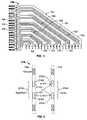
- FIG. 1is a perspective view of an orthogonal connector system formed in accordance with an exemplary embodiment of the present invention.
- FIG. 2is a perspective view one of the receptacle connectors shown in FIG. 1 .
- FIG. 3is a front elevational view of a lead frame formed in accordance with an exemplary embodiment of the present invention.
- FIG. 4is a schematic two-pair cross-section of a first connector assembly formed in accordance with an exemplary embodiment of the present invention.
- FIG. 5is a schematic two-pair cross-section of a second connector assembly formed in accordance with an exemplary embodiment of the present invention.
- FIG. 6is a schematic two-pair cross-section of a second connector assembly formed in accordance with an alternative embodiment of the present invention.
- FIG. 7is a schematic view of an exemplary signal path through a connector system.
- FIG. 8is a perspective view of a header connector formed in accordance with an exemplary embodiment of the present invention.
- FIG. 9is a perspective view of an exemplary header connector ground contact.
- FIG. 10is a perspective view of an exemplary header connector offset signal contact.
- FIG. 11is a perspective view of an exemplary header connector straight signal contact.
- FIG. 12is a top plan view of the mounting end of the header connector shown in FIG. 8 .
- FIG. 13is a perspective view of a mounted pair of offset signal contacts.
- FIG. 14is a top plan view of the via pattern of a midplane board.
- FIG. 1illustrates an orthogonal connector system 100 .
- the connector system 100includes a first connector assembly 102 and a second connector assembly 104 .
- the connector assemblies 102 and 104are orthogonal connector to one another.
- the connector assemblies 102 and 104are mounted on a midplane circuit board 110 which is shown in phantom lines for clarity.
- the first connector assembly 102includes a first receptacle connector 120 and a first header connector 122 .
- the second connector assembly 104includes a second header connector 126 , and a second receptacle connector 128 .
- the first header and receptacle connectors 122 and 120are mounted on a first side 132 of the midplane 110 and connect through the midplane 110 to the second header and receptacle connectors 126 and 128 , respectively, which are mounted on a second side 134 of the midplane 110 .
- the first receptacle connector 120includes a daughter card interface 140 .
- the first receptacle 120may be mounted on a line card (not shown) at the interface 140 .
- the second receptacle connector 128includes a daughter card interface 142 and, by way of example only, the second receptacle 128 may be mounted on a switch card (not shown) at the interface 142 .
- the connector system 100includes a longitudinal axis A that extends from the first receptacle 120 through the second receptacle 128 .
- the first and second header connectors 122 and 126are identical to one another.
- the first and second receptacle connectors 120 and 128may or may not be identical to one another.
- the first and second header connectors 122 and 126are oriented such that the first and second header connectors 122 and 126 are rotated ninety degrees with respect to one another to form the orthogonal connector system 100 .
- the first and second receptacles 120 and 128are likewise rotated ninety degrees with respect to one another.
- the orthogonal orientation of the connector system 100facilitates the elimination of traces within the midplane and reduces signal loss through the connector system 100 .
- the connector system 100is also configured to cancel far end crosstalk generated in the connector system 100 in differential signals transmitted through the connector system 100 , as will be described.
- FIG. 2illustrates a perspective view of the receptacle connector 120 .
- FIG. 3illustrates a lead frame 148 that is contained in the receptacle connector 120 .
- the receptacle connector 120includes a dielectric housing 150 that has a mating face 154 having a plurality of contact channels 156 .
- the contact channels 156are configured to receive mating contacts 350 , 352 , 390 (see FIG. 8 ) from a mating header connector such as the header connector 122 shown in FIG. 1 .
- the receptacle connector 120also includes an upper shroud 158 that extends rearwardly from the mating face 154 .
- Guide ribs 160are formed on opposite sides of the housing 150 to orient the receptacle connector 120 for mating with the header connector 122 .
- An alignment recess 161is provided on each side of the guide rib 160 .
- the housing 150receives a plurality of contact modules or chicklets 162 holding contacts that connect the daughter card interface 140 with the mating face 154 .
- the interface 140is substantially perpendicular to the mating face 154 such that the receptacle connector 120 interconnects electrical components that are substantially at a right angle to each other.
- Each chicklet 162includes a contact lead frame such as the lead frame 148 that is overmolded and encased in a contact module housing 170 fabricated from a dielectric material.
- the housing 170has a forward mating end (not shown) that is received in the receptacle connector housing 150 and a mounting edge 174 configured for mounting to a circuit board.
- Contact tails 176extend from the lead frame within the contact module 162 and extend through the mounting edge 174 of the contact module 162 for attachment to a circuit board (not shown).
- the contact lead frame 148includes a plurality of conductive leads 182 terminating at one end with a mating contact 184 and terminating at the other end with the mounting contact tails 176 .
- the contact lead frame 148includes pairs of signal leads 190 and individual ground leads 192 arranged in an alternating sequence wherein individual ground leads 192 separate pairs of signal leads 190 from one another.
- the signal lead pairs 190 and ground leads 192may be offset relative to the signal lead pairs 190 and ground leads 192 in an adjacent chicklet, although the alternating pattern is maintained.
- the signal lead pairs 190carry and transmit differential signals and each of the signal lead pairs 190 comprises a differential pair 190 .
- any of the signal lead pairs 190when switching or transmitting a signal, has the potential to produce crosstalk in an adjacent signal lead pair 190 with the level of crosstalk being a function of proximity or distance between the transmitting signal lead pair 190 and the adjacent signal lead pair 190 .
- the crosstalk generated in the connector assemblies, 102 and 104may be cancelled if the leads of one signal lead pair 190 in one of the connector assemblies 102 , 104 are inverted or flipped with respect to the adjacent signal lead pair 190 in the other of the connector assemblies 102 , 104 as will be described.
- FIGS. 4 , 5 , and 6illustrate crosstalk cancellation in accordance with the present invention.
- FIG. 4illustrates a schematic two-pair cross-section of a mated first connector assembly 200 formed in accordance with an exemplary embodiment of the present invention.
- FIG. 5illustrates a schematic two-pair cross-section of a mated second connector assembly 204 that is orthogonal to the first connector assembly 200 .
- Each connector assembly 200 and 204represents a mated header and receptacle connector pair.
- the connector assembly 200includes a chicklet 208 which is shown in phantom lines.
- the chicklet 208includes a differential signal pair 210 A that by way of example is designated an aggressor signal pair that, at a point in time, is switching or transmitting a signal.
- An adjacent chicklet 212also shown in phantom lines, in the connector assembly 200 includes a differential signal pair 214 A that is adjacent to the signal pair 210 A.
- the signal pair 214 Ais not switching and is designated a victim signal pair.
- the aggressor signal pair 210 Ais generating crosstalk in the victim signal pair 214 A as a result of electromagnetic energy coupling between the pairs.
- the crosstalk in the victim signal pair 214 A that propagates in the same direction as the signal in the aggressor signal pair 210 Ais referred to as far end crosstalk. When the far end crosstalk reaches the receiver (not shown) of the victim signal pair, the crosstalk can erroneously be detected as a switch in the victim signal.
- the lines of the aggressor signal pair 210 Aare labeled 216 A which is designated + and 218 A which is designated ⁇ .
- the signal lines of the victim signal pairare labeled 220 A which is designated + and 222 A which is designated ⁇ .
- a, b, c, and drepresent crosstalk energy components and may be measured as voltages coupled between signal pairs.
- e, f, g, and hrepresent crosstalk energy components and may be measured as voltages coupled between signal pairs.
- the differential crosstalk on the victim signal pair 214 Amay be expressed as the sum of the energy components (a+d) coupled onto the positive signal line 220 A minus the sum of the energy components (b+c) coupled onto the negative signal line 222 A, or (a+d) ⁇ (b+c). If a and b are positive coupling values, then c and d are negative coupling values since the aggressor signal pair 210 A is a differential signal pair.
- the aggressor signal pair 210 Bis located in a chicklet 230 .
- the victim signal pair 214 Bis located in a chicklet 232 .
- the + and ⁇ signal lines 216 B and 218 B, respectively, of the aggressor signal pair 210 Bare inverted with respect to the + and ⁇ signal lines 220 B and 222 B, respectively, of the victim signal pair 214 B.
- This relationshipis inverse to the relationship of the aggressor and victim signal pairs in the first connector assembly 200 . That is, the ⁇ aggressor signal line 218 B is now in closest proximity to the + victim signal line 220 B and the + aggressor signal line 216 B is now in closest proximity to the ⁇ victim signal line 222 B.
- the differential crosstalk on the victim signal pair 214 Bis (e+h), the energy coupled onto 220 B minus (f+g), the energy coupled onto 222 B, or (e+h) ⁇ (f+g). And again, if g and h are positive crosstalk coupling values, then e and f are negative crosstalk coupling values.
- the connector assemblies 200 and 204are orthogonal connector assemblies, the far end crosstalk, or the crosstalk propagated in the same direction as the aggressor signal from the first connector assembly 200 to the second connector assembly 204 , is canceled. Cancellation occurs because the signal carried by the aggressor signal pair 210 A is the same signal as in the aggressor signal pair 210 B, i.e.
- FIG. 6illustrates a schematic two-pair cross-section of a second connector assembly 240 formed in accordance with an alternative embodiment of the present invention.
- the connector assembly 240comprises a mated header and receptacle connector that are orthogonal to the connector assembly 200 ( FIG. 4 ).
- the connector assembly 240is configured such that the ⁇ signal line 218 B of the aggressor signal pair 210 B and the + signal line 220 B of the victim signal pair 214 B are located in a chicklet 242 .
- the + signal line 216 B of the aggressor signal pair 210 B and the ⁇ signal line 222 B of the victim signal pair 214 Bare located in a chicklet 244 .
- the connector assembly 204FIG.
- the + and ⁇ signal lines 216 B and 218 B, respectively, of the aggressor signal pair 210 B and 220 B and 222 B, respectively, of the victim signal pair 214 Bare inverted from their relationship to one another in the first connector assembly 200 . That is, the ⁇ aggressor signal line 218 B is now in closest proximity to the + victim signal line 220 B and the + aggressor signal line 216 B is now in closest proximity to the ⁇ victim signal line 222 B.
- the differential crosstalk on the victim signal pair 214 Bis (e+h) ⁇ (f+g), and again, if g and h are positive crosstalk coupling values, then e and f are negative crosstalk coupling values.
- FIG. 7is a schematic view of an exemplary signal path through a connector system 300 that includes the first connector assembly 200 shown in FIG. 4 and the second connector assembly 204 , shown in FIG. 5 .
- the first connector assembly 200is mounted on a circuit board 302 .
- the second connector assembly 204is mounted on a circuit board 304 .
- the first and second connector assemblies 200 and 204are orthogonal assemblies and are connected to one another through the midplane 110 .
- the first and second connector assemblies 200 and 204respectively, each include contacts arranged in at least two differential pairs wherein one of the pairs is an aggressor pair 210 A, 210 B and one of the pairs is a victim pair 214 A, 214 B, wherein a differential signal carried by the aggressor pair 210 A, 210 B generates far end crosstalk on the victim pair 214 A, 214 B.
- Contacts 350 , 352are arranged such that, when the first and second connector assemblies 200 , 204 , respectively, are electrically connected to each other, the far end crosstalk on the victim pair 214 A in the first connector assembly 200 has a magnitude and a polarity, and the far end crosstalk on the victim pair 214 B in the second connector assembly 204 has the same magnitude and an opposite polarity so that the far end crosstalk in the second connector assembly 204 cancels the far end crosstalk in the first connector assembly 200 .
- the first connector assembly 200includes a first lead frame 310 that includes ground leads 312 and the differential signal pair 210 A with the signal leads 216 A and 218 A.
- a second lead frame 320includes ground leads 322 and the differential signal pair 214 A with the signal leads 220 A and 222 A.
- the second connector assembly 204includes a first lead frame 330 that includes ground leads 332 and the differential signal pair 210 B with the signal leads 216 B and 218 B.
- a second lead frame 340includes ground leads 342 and the differential signal pair 214 B with the signal leads 220 B and 222 B.
- the signal leads 216 A and 218 Aare connected through header contacts 350 at the midplane 110 to the signal leads 216 B and 218 B respectively.
- the signal leads 220 A and 222 Aconnect through header contacts 352 at the midplane 110 to the signal leads 220 B and 222 B respectively.
- the signal leads 216 B and 218 Bare inverted with respect to one another as compared to the signal leads 216 A and 218 A, while the relationship of the signal leads 220 B and 222 B with respect to one another as compared to the signal leads 220 A and 222 A is unchanged. In this manner, far end crosstalk from one differential signal pair to an adjacent differential signal pair in the first connector assembly 200 is canceled in the second connector assembly 204 .
- the inversion of the signal leads 216 B and 218 B with respect to the signal leads 216 A and 218 Ais accomplished with the header contacts 350 at their connection to the midplane 110 as described below.
- FIG. 8illustrates a perspective view of the header connector 122 .
- the header connector 122includes a dielectric housing 370 having a mating end 372 that receives the receptacle connector 120 and a mounting end 374 for mounting the header connector 122 to the midplane board 110 ( FIG. 7 ).
- the housing 370includes opposite shrouds 378 and opposite shrouds 380 that cooperate to surround the mating end 372 .
- Guide slots 384are provided on the shrouds 380 that receive the guide ribs 160 on the receptacle connector 120 ( FIG. 2 ) to orient the receptacle connector 120 with respect to the header connector 122 .
- Alignment pads 386are formed on the interior surfaces 388 of the shrouds 380 . The alignment pads 386 are received in the alignment recesses 161 on the receptacle connector 120 to further assure proper orientation of the receptacle connector 120 with respect to the header connector 122 .
- the header connector 122holds a plurality of electrical contacts including ground contacts 390 and two configurations of signal contacts 350 and 352 .
- the signal contacts 352are straight signal contacts.
- the signal contacts 350are offset signal contacts that, when used in corresponding pairs on opposite sides of a midplane 110 ( FIG. 7 ), can invert a pair of mating signal leads with respect to one another from one side of the midplane 110 to the other as will be described.
- the ground contacts 390are longer than the signal contacts 350 and 352 so that the ground contacts 390 are the first to mate and last to break when the header connector 122 is mated and separated, respectively, with the receptacle connector 120 ( FIG. 2 ).
- the contacts 350 , 352 , and 390are arranged in rows including pairs of signal contacts 350 , 352 and individual ground contacts 390 arranged in an alternating sequence. Within the alternating sequence, the pairs of signal contacts 350 , 352 also alternate. For instance, in FIG. 8 , the first contact row includes a ground contact 390 , a pair of signal contacts 350 , a ground contact 390 , then a pair of signal contacts 352 , etc. The order of the signal contacts 350 and 352 also alternates in adjacent contact rows.
- FIG. 9illustrates an exemplary ground contact 390 which may be used, for example, in the header connector 122 (shown in FIG. 8 ).
- the ground contact 390includes a mating end 400 , a mid-section 402 , and a mounting end 404 .
- the mating end 400includes a blade section 406 that is configured to be matable with a ground contact in a mating receptacle connector 120 ( FIG. 1 ).
- the mid-section 402is configured for press fit installation in the housing 370 ( FIG. 8 ).
- the mid-section 402includes retention barbs 408 that retain the ground contact 390 in the housing 370 .
- the ground contact 390is of straight construction wherein the mating end 400 , mid-section 402 , and mounting end 404 all lie along a common centerline 409 .
- the mounting end 404extends from the housing 370 and is provided for mounting the header connector 122 on a circuit board, such as the midplane board 110 ( FIG. 7 ) or a panel, or the like.
- the mounting end 404is a compliant eye of the needle design.
- FIG. 10illustrates a perspective view of the offset signal contact 350 that is configured to invert a differential signal lead pair from one side of the midplane 110 ( FIG. 7 ) to the other when used in a pair of header connectors mated either directly or through a midplane as shown for example in FIG. 7 .
- the offset signal contact 350includes a mating end 410 , a mid-section 412 , and a mounting end 414 .
- the mating end 410includes a blade section 416 that is configured to be matable with a signal contact in a mating receptacle connector 120 ( FIG. 1 ).
- the blade section 416 and mid-section 412extend along a longitudinal centerline 418 and lie in a plane 420 .
- a plate 430extends from the mid-section 412 and the mounting end 414 extends from the plate 430 along a longitudinal centerline 432 such that the mounting end 414 is offset from the mating end 410 and mid-section 412 .
- the plate 430is formed at an angle 434 with the plane 420 of the blade section 416 . In the exemplary embodiment, the angle 434 is about forty-five degrees.
- the plate 430shifts the mounting end 414 out of alignment with the mating end 410 of the signal contact 350 .
- the mounting end 414extends from the housing 370 and is provided for mounting the header connector 122 to a circuit board, such as the midplane board 110 ( FIG. 7 ) or a panel, or the like. In an exemplary embodiment, the mounting end 414 is a compliant eye of the needle design.
- the mid-section 412may also include one or more retention barbs 436 to hold the signal contact 350 in the header connector housing 370 .
- FIG. 11illustrates an exemplary straight signal contact 352 which may be used, for example, in the header connector 122 (shown in FIG. 8 ).
- the straight signal contact 352includes a mating end 450 , a mid-section 452 , and a mounting end 454 .
- the mating end 450includes a blade section 456 that is configured to be matable with a signal contact in a mating receptacle connector 120 ( FIG. 1 ).
- the mid-section 452is configured for press fit installation in the housing 370 ( FIG. 8 ).
- the mid-section 452includes retention barbs 458 that retain the straight signal contact 352 in the housing 370 .
- the straight signal contact 352is of straight construction wherein the mating end 450 , mid-section 452 , and mounting end 454 all lie along a common centerline 460 .
- the mounting end 454extends from the housing 370 and is provided for mounting the header connector 122 on a circuit board, such as the midplane board 110 ( FIG. 7 ) or a panel, or the like.
- the mounting end 404is a compliant eye of the needle design.
- the straight signal contact 352is similar to the ground contact 390 with the exception that the blade section 406 of the ground contact 390 is longer than the blade section 456 of the straight signal contact 352 .
- FIG. 12illustrates a bottom plan view of the mounting end 374 of the header connector 122 .
- the header connector housing 370includes a base 500 having a plurality of contact cavities arranged in rows 502 .
- Each row 502 of contact cavitiesincludes ground contact cavities 504 , pairs of straight signal contact cavities 506 , and pairs of offset signal contact cavities 508 , each of which receives a respective ground contact 390 , straight signal contact 352 , and offset signal contact 350 ( FIG. 8 ).
- the contact cavitiesare formed in an alternating sequence of individual ground contact cavities 504 and pairs of straight signal contact cavities 506 alternated with pairs of offset signal contact cavities 508 as described above with respect to the signal and ground contacts 350 , 352 and 390 .
- Each contact cavity row 502extends along a centerline 510 .
- Each offset contact cavity 508includes a slot 512 that is sized to receive the plate 430 on the offset signal contact 350 .
- the slotsextend at an angle 514 that is substantially the same as the angle 434 and which is about forty-five degrees.
- Each of the slots 512 within an adjacent pair of offset contact cavities 508extend in opposite directions from the centerline 510 .
- the offset signal contacts 350are loaded into the connector housing such that the plates 430 of adjacent contacts 350 within a contact pair extend in opposite directions from the contact row centerline 510 .
- Distal ends 516 of each adjacent pair of slots 512define a line 520 therebetween that is substantially perpendicular to the centerline 510 .
- Each contact cavity column 530extend across the housing base 500 in the direction of the arrow 532 which is substantially perpendicular to the contact rows centerline 510 .
- Each contact cavity column 530receives only signal contacts 350 , 352 or ground contacts 390 ( FIG. 8 ).
- the signal and ground contacts 350 , 352 , and 390are configured to be received in vias in the midplane board 110 ( FIG. 7 ).
- the signal contacts 350 and 352are received in through vias to electrically connect with signal contacts in a header connector on the other side of the midplane board 110 .
- the ground contacts 390may or may not share vias in the midplane board 110 . In some embodiments, the ground contacts 390 may be configured to electrically engage at least one ground plane in the midplane board 110 .
- the ground planesprovide continuity between the ground contacts 390 in the header connector 122 from one side 132 of the midplane board 110 to the ground contacts in a header connector such as the header connector 126 ( FIG. 1 ) on other side 134 of the midplane board 110 .
- FIG. 13is a perspective view of two mated pair 550 and 552 of offset signal contacts.
- a contact pair 550is electrically connected to the contact pair 552 through vias 554 in the midplane 110 and carries differential signals.
- the contact pair 550includes offset contacts 350 A and 350 B and is located on one side 132 of the midplane 110 .
- the contact pair 552includes offset contacts 350 C and 350 D and is located on the other side 134 of the midplane 110 .
- the contacts 350 A, 350 B, 350 C, and 350 D of each contact pair 550 and 552are arranged about a common axis 570 .
- the contacts 350 A, 350 B, 350 C, and 350 Dare oriented such that the contact 350 A of the contact pair 550 is electrically connected to the contact 350 D of the contact pair 552 and the contact 350 B is electrically connected to the contact 350 C of the contact pair 552 .
- the contact 350 C of the contact pair 552is offset one hundred eighty degrees about the axis 570 with respect to the contact 350 B to which it is electrically connected in the contact pair 550 .
- the contact 350 D of the contact pair 552is offset one hundred eighty degrees about the axis 570 with respect to the contact 350 A to which it is electrically connected in the contact pair 550 .
- the contact pair 550 on one side 132 of the midplane 110is effectively inverted or flipped with respect to the mating contact pair 552 on the other side 134 of the midplane 110 .
- the relative position of one contact pair, such as the contact pair 550 having offset contacts 350 A, 350 Bis inverted with respect to an adjacent contact an adjacent contact pair (not shown) having straight contacts such as the contact 352 ( FIG. 11 ).
- a connectorsuch as the connector 122 ( FIG. 8 ) that has alternating pairs of straight signal contacts 352 ( FIG. 11 ) and offset signal contacts 350 ( FIG. 10 ), any far end crosstalk from the signals carried in an adjacent contact pair (see FIG.
- FIG. 14is a top plan view of the via pattern on one side 132 of the midplane board 110 .
- the via patternincludes pairs of signal vias 580 , 582 and individual ground vias 584 .
- the via patternincludes vias arranged in rows 588 that extend in the direction of the arrow 590 and columns 592 that extend in the direction of the arrow 594 which is substantially perpendicular to the direction of the arrow 590 .
- the signal vias 580are configured to receive the offset signal contacts 350 ( FIG. 10 ).
- the signal vias 582are configured to receive the straight signal contacts 352 ( FIG. 7 ).
- Each pair of signal vias 580includes individual vias 600 that are arranged along a centerline 602 that is substantially perpendicular to the direction 590 of the rows 588 . That is, the signal via pairs 580 are rotated ninety degrees from the orientation of the signal via pairs 582 . By contrast, individual vias 606 in each signal via pair 582 are aligned in the direction 590 of the rows 588 .
- ground vias 584 and pairs of signal vias 580 and 582are arranged in an alternating sequence. Within the sequence, the signal via pairs 580 alternate with signal via pairs 582 to yield a sequence such as: ground via 584 , signal via pair 580 , ground via 584 , signal via pair 582 , ground via 584 , etc. In addition, the signal via pairs 580 and 582 are offset from one another in adjacent rows 588 .
- the signal vias 600 and 606are through vias that receive a signal contacts 350 , 352 ( FIG. 7 ) at each end to directly interconnect signal contacts 350 , 352 on each side of the midplane 110 .
- ground vias 584in some embodiments are through vias that directly interconnect ground contacts 390 on each side of the midplane 110 . In other embodiments, one or more ground vias 584 may electrically engage one or more ground planes in the midplane 110 .
- Each via column 592includes vias that are either all ground vias 584 or all alternating pairs of signal vias 580 , 582 .
- the embodiments thus describedprovide a connector that cancels far end crosstalk when used in a system of two mated pairs of orthogonal connectors.
- the connectoris suitable for use in orthogonal systems designed to carry differential signals.
- the connectorincludes alternating offset signal contact pairs and straight signal contact pairs. Corresponding offset signal pairs on opposite sides of a midplane or panel cooperate to invert or flip the orientation of a differential signal pair to cancel the crosstalk coupled from an adjacent differential signal pair as the signals are transmitted through the connector.
Landscapes
- Details Of Connecting Devices For Male And Female Coupling (AREA)
- Coupling Device And Connection With Printed Circuit (AREA)
Abstract
Description
Claims (15)
Priority Applications (7)
| Application Number | Priority Date | Filing Date | Title |
|---|---|---|---|
| US11/726,346US7621781B2 (en) | 2007-03-20 | 2007-03-20 | Electrical connector with crosstalk canceling features |
| CN2008800087578ACN101636881B (en) | 2007-03-20 | 2008-03-14 | Electrical Connectors with Crosstalk Cancellation Properties |
| DE602008002429TDE602008002429D1 (en) | 2007-03-20 | 2008-03-14 | ELECTRICAL CONNECTOR WITH TRANSMIT EXPRESSION FEATURES |
| AT08726844TATE480027T1 (en) | 2007-03-20 | 2008-03-14 | ELECTRICAL CONNECTOR WITH CROSSTALK CANCELING FEATURES |
| PCT/US2008/003411WO2008115422A2 (en) | 2007-03-20 | 2008-03-14 | Electrical connector with crosstalk canceling features |
| EP08726844AEP2140525B1 (en) | 2007-03-20 | 2008-03-14 | Electrical connector with crosstalk canceling features |
| TW097109433ATWI412182B (en) | 2007-03-20 | 2008-03-18 | Electrical connector with crosstalk canceling features |
Applications Claiming Priority (1)
| Application Number | Priority Date | Filing Date | Title |
|---|---|---|---|
| US11/726,346US7621781B2 (en) | 2007-03-20 | 2007-03-20 | Electrical connector with crosstalk canceling features |
Publications (2)
| Publication Number | Publication Date |
|---|---|
| US20080233806A1 US20080233806A1 (en) | 2008-09-25 |
| US7621781B2true US7621781B2 (en) | 2009-11-24 |
Family
ID=39739288
Family Applications (1)
| Application Number | Title | Priority Date | Filing Date |
|---|---|---|---|
| US11/726,346ActiveUS7621781B2 (en) | 2007-03-20 | 2007-03-20 | Electrical connector with crosstalk canceling features |
Country Status (7)
| Country | Link |
|---|---|
| US (1) | US7621781B2 (en) |
| EP (1) | EP2140525B1 (en) |
| CN (1) | CN101636881B (en) |
| AT (1) | ATE480027T1 (en) |
| DE (1) | DE602008002429D1 (en) |
| TW (1) | TWI412182B (en) |
| WO (1) | WO2008115422A2 (en) |
Cited By (29)
| Publication number | Priority date | Publication date | Assignee | Title |
|---|---|---|---|---|
| US20080315985A1 (en)* | 2007-06-22 | 2008-12-25 | Sun Microsystems, Inc. | Multi-switch chassis |
| US20090159314A1 (en)* | 2006-12-19 | 2009-06-25 | Minich Steven E | Shieldless, high-speed, low-cross-talk electrical connector |
| US20120058655A1 (en)* | 2010-09-08 | 2012-03-08 | Hon Hai Precision Industry Co., Ltd. | Electrical connector with improved impedance continuity |
| CN102544954A (en)* | 2010-11-11 | 2012-07-04 | 泰科电子公司 | Cable assembly for a connector system |
| US8267721B2 (en) | 2009-10-28 | 2012-09-18 | Fci Americas Technology Llc | Electrical connector having ground plates and ground coupling bar |
| US20130034978A1 (en)* | 2011-08-01 | 2013-02-07 | Lemke Timothy A | Crosstalk Reduction |
| WO2013006247A3 (en)* | 2011-07-01 | 2013-03-07 | Fci | Connection footprint for electrical connector with printed wiring board |
| US20130288521A1 (en)* | 2012-04-26 | 2013-10-31 | Tyco Electronics Corporation | Contact modules for receptacle assemblies |
| US20130288539A1 (en)* | 2012-04-26 | 2013-10-31 | Tyco Electronics Coporation | Receptacle assembly for a midplane connector system |
| US8579636B2 (en)* | 2012-02-09 | 2013-11-12 | Tyco Electronics Corporation | Midplane orthogonal connector system |
| US20130323969A1 (en)* | 2012-06-01 | 2013-12-05 | Alps Electric Co., Ltd. | Socket for electronic components |
| US8616919B2 (en) | 2009-11-13 | 2013-12-31 | Fci Americas Technology Llc | Attachment system for electrical connector |
| US8764464B2 (en) | 2008-02-29 | 2014-07-01 | Fci Americas Technology Llc | Cross talk reduction for high speed electrical connectors |
| US8864516B2 (en) | 2012-02-24 | 2014-10-21 | Tyco Electronics Corporation | Cable assembly for interconnecting card modules in a communication system |
| USD718253S1 (en) | 2012-04-13 | 2014-11-25 | Fci Americas Technology Llc | Electrical cable connector |
| US8905651B2 (en) | 2012-01-31 | 2014-12-09 | Fci | Dismountable optical coupling device |
| USD720698S1 (en) | 2013-03-15 | 2015-01-06 | Fci Americas Technology Llc | Electrical cable connector |
| US8944831B2 (en) | 2012-04-13 | 2015-02-03 | Fci Americas Technology Llc | Electrical connector having ribbed ground plate with engagement members |
| USD727268S1 (en) | 2012-04-13 | 2015-04-21 | Fci Americas Technology Llc | Vertical electrical connector |
| USD727852S1 (en) | 2012-04-13 | 2015-04-28 | Fci Americas Technology Llc | Ground shield for a right angle electrical connector |
| US9048583B2 (en) | 2009-03-19 | 2015-06-02 | Fci Americas Technology Llc | Electrical connector having ribbed ground plate |
| USD733662S1 (en) | 2013-01-25 | 2015-07-07 | Fci Americas Technology Llc | Connector housing for electrical connector |
| USD746236S1 (en) | 2012-07-11 | 2015-12-29 | Fci Americas Technology Llc | Electrical connector housing |
| US9257778B2 (en) | 2012-04-13 | 2016-02-09 | Fci Americas Technology | High speed electrical connector |
| US9277649B2 (en) | 2009-02-26 | 2016-03-01 | Fci Americas Technology Llc | Cross talk reduction for high-speed electrical connectors |
| US9520661B1 (en)* | 2015-08-25 | 2016-12-13 | Tyco Electronics Corporation | Electrical connector assembly |
| US9543703B2 (en) | 2012-07-11 | 2017-01-10 | Fci Americas Technology Llc | Electrical connector with reduced stack height |
| US10199774B2 (en) | 2015-03-06 | 2019-02-05 | Molex, Llc | Connector and system with short signal pins |
| US20240145994A1 (en)* | 2022-10-28 | 2024-05-02 | Te Connectivity Solutions Gmbh | Interconnection System for Ground Current Optimization |
Families Citing this family (20)
| Publication number | Priority date | Publication date | Assignee | Title |
|---|---|---|---|---|
| CN101378618B (en)* | 2007-08-31 | 2010-09-29 | 鸿富锦精密工业(深圳)有限公司 | A printed circuit board |
| US7666009B2 (en)* | 2008-02-08 | 2010-02-23 | Fci Americas Technology, Inc. | Shared hole orthogonal footprints |
| JP5155700B2 (en)* | 2008-03-11 | 2013-03-06 | 富士通コンポーネント株式会社 | connector |
| US7736183B2 (en)* | 2008-10-13 | 2010-06-15 | Tyco Electronics Corporation | Connector assembly with variable stack heights having power and signal contacts |
| US7867032B2 (en)* | 2008-10-13 | 2011-01-11 | Tyco Electronics Corporation | Connector assembly having signal and coaxial contacts |
| US7744431B2 (en)* | 2008-10-13 | 2010-06-29 | Tyco Electronics Corporation | Receptacle contact with a widened mating tip |
| US7637777B1 (en)* | 2008-10-13 | 2009-12-29 | Tyco Electronics Corporation | Connector assembly having a noise-reducing contact pattern |
| US7740489B2 (en)* | 2008-10-13 | 2010-06-22 | Tyco Electronics Corporation | Connector assembly having a compressive coupling member |
| US7896698B2 (en)* | 2008-10-13 | 2011-03-01 | Tyco Electronics Corporation | Connector assembly having multiple contact arrangements |
| US8357013B2 (en)* | 2009-01-22 | 2013-01-22 | Hirose Electric Co., Ltd. | Reducing far-end crosstalk in electrical connectors |
| US8113851B2 (en)* | 2009-04-23 | 2012-02-14 | Tyco Electronics Corporation | Connector assemblies and systems including flexible circuits |
| US8079847B2 (en)* | 2009-06-01 | 2011-12-20 | Tyco Electronics Corporation | Orthogonal connector system with power connection |
| US8905785B2 (en) | 2009-12-30 | 2014-12-09 | Fci Americas Technology Llc | Electrical connector having conductive housing |
| US7963776B1 (en)* | 2010-03-23 | 2011-06-21 | Tyco Electronics Corporation | Electrical connector assembly having direct connection terminals |
| US7918683B1 (en) | 2010-03-24 | 2011-04-05 | Tyco Electronics Corporation | Connector assemblies and daughter card assemblies configured to engage each other along a side interface |
| US8500487B2 (en)* | 2011-11-15 | 2013-08-06 | Tyco Electronics Corporation | Grounding structures for header and receptacle assemblies |
| US8992252B2 (en)* | 2012-04-26 | 2015-03-31 | Tyco Electronics Corporation | Receptacle assembly for a midplane connector system |
| EP2797179A1 (en) | 2013-04-24 | 2014-10-29 | Koninklijke Philips N.V. | Inductive disturbance reduction device |
| US9413097B2 (en)* | 2014-12-22 | 2016-08-09 | Intel Corporation | High density cabled midplanes and backplanes |
| CN107565278A (en)* | 2017-08-25 | 2018-01-09 | 郑州云海信息技术有限公司 | A kind of high speed connector leg signal crosstalk processing method and processing device |
Citations (8)
| Publication number | Priority date | Publication date | Assignee | Title |
|---|---|---|---|---|
| US5224867A (en)* | 1990-10-08 | 1993-07-06 | Daiichi Denshi Kogyo Kabushiki Kaisha | Electrical connector for coaxial flat cable |
| US6976886B2 (en)* | 2001-11-14 | 2005-12-20 | Fci Americas Technology, Inc. | Cross talk reduction and impedance-matching for high speed electrical connectors |
| US20060024984A1 (en) | 2004-07-01 | 2006-02-02 | Cohen Thomas S | Midplane especially applicable to an orthogonal architecture electronic system |
| US20060068641A1 (en)* | 2003-09-26 | 2006-03-30 | Hull Gregory A | Impedance mathing interface for electrical connectors |
| US20070059961A1 (en) | 2005-06-30 | 2007-03-15 | Cartier Marc B | Electrical connector for interconnection assembly |
| EP1783871A1 (en) | 2005-11-02 | 2007-05-09 | Tyco Electronics Corporation | Orthogonal connector |
| US20080207023A1 (en)* | 2005-06-08 | 2008-08-28 | Jacobus Nicolaas Tuin | Electrical Connector |
| WO2008106096A1 (en) | 2007-02-28 | 2008-09-04 | Fci | Orthogonal header |
Family Cites Families (2)
| Publication number | Priority date | Publication date | Assignee | Title |
|---|---|---|---|---|
| US7131870B2 (en)* | 2005-02-07 | 2006-11-07 | Tyco Electronics Corporation | Electrical connector |
| TW200644346A (en)* | 2005-04-07 | 2006-12-16 | Fci Americas Technology Inc | Orthogonal backplane connector |
- 2007
- 2007-03-20USUS11/726,346patent/US7621781B2/enactiveActive
- 2008
- 2008-03-14ATAT08726844Tpatent/ATE480027T1/ennot_activeIP Right Cessation
- 2008-03-14EPEP08726844Apatent/EP2140525B1/ennot_activeNot-in-force
- 2008-03-14WOPCT/US2008/003411patent/WO2008115422A2/enactiveApplication Filing
- 2008-03-14CNCN2008800087578Apatent/CN101636881B/ennot_activeExpired - Fee Related
- 2008-03-14DEDE602008002429Tpatent/DE602008002429D1/enactiveActive
- 2008-03-18TWTW097109433Apatent/TWI412182B/ennot_activeIP Right Cessation
Patent Citations (10)
| Publication number | Priority date | Publication date | Assignee | Title |
|---|---|---|---|---|
| US5224867A (en)* | 1990-10-08 | 1993-07-06 | Daiichi Denshi Kogyo Kabushiki Kaisha | Electrical connector for coaxial flat cable |
| US6976886B2 (en)* | 2001-11-14 | 2005-12-20 | Fci Americas Technology, Inc. | Cross talk reduction and impedance-matching for high speed electrical connectors |
| US20080248693A1 (en)* | 2001-11-14 | 2008-10-09 | Fci Americas Technology, Inc. | Shieldless, high-speed electrical connectors |
| US20060068641A1 (en)* | 2003-09-26 | 2006-03-30 | Hull Gregory A | Impedance mathing interface for electrical connectors |
| US20060024984A1 (en) | 2004-07-01 | 2006-02-02 | Cohen Thomas S | Midplane especially applicable to an orthogonal architecture electronic system |
| US20070149057A1 (en)* | 2004-07-01 | 2007-06-28 | Amphenol Corpoation | Midplane especially applicable to an orthogonal architecture electronic system |
| US20080207023A1 (en)* | 2005-06-08 | 2008-08-28 | Jacobus Nicolaas Tuin | Electrical Connector |
| US20070059961A1 (en) | 2005-06-30 | 2007-03-15 | Cartier Marc B | Electrical connector for interconnection assembly |
| EP1783871A1 (en) | 2005-11-02 | 2007-05-09 | Tyco Electronics Corporation | Orthogonal connector |
| WO2008106096A1 (en) | 2007-02-28 | 2008-09-04 | Fci | Orthogonal header |
Non-Patent Citations (1)
| Title |
|---|
| International Search Report, International Application No. PCT/US2008/003411, International Filing Date Mar. 14, 2008. |
Cited By (60)
| Publication number | Priority date | Publication date | Assignee | Title |
|---|---|---|---|---|
| US8382521B2 (en) | 2006-12-19 | 2013-02-26 | Fci Americas Technology Llc | Shieldless, high-speed, low-cross-talk electrical connector |
| US20090159314A1 (en)* | 2006-12-19 | 2009-06-25 | Minich Steven E | Shieldless, high-speed, low-cross-talk electrical connector |
| US7762843B2 (en) | 2006-12-19 | 2010-07-27 | Fci Americas Technology, Inc. | Shieldless, high-speed, low-cross-talk electrical connector |
| US8096832B2 (en) | 2006-12-19 | 2012-01-17 | Fci Americas Technology Llc | Shieldless, high-speed, low-cross-talk electrical connector |
| US8678860B2 (en) | 2006-12-19 | 2014-03-25 | Fci Americas Technology Llc | Shieldless, high-speed, low-cross-talk electrical connector |
| US20080315985A1 (en)* | 2007-06-22 | 2008-12-25 | Sun Microsystems, Inc. | Multi-switch chassis |
| US8764464B2 (en) | 2008-02-29 | 2014-07-01 | Fci Americas Technology Llc | Cross talk reduction for high speed electrical connectors |
| US9277649B2 (en) | 2009-02-26 | 2016-03-01 | Fci Americas Technology Llc | Cross talk reduction for high-speed electrical connectors |
| US10720721B2 (en) | 2009-03-19 | 2020-07-21 | Fci Usa Llc | Electrical connector having ribbed ground plate |
| US9048583B2 (en) | 2009-03-19 | 2015-06-02 | Fci Americas Technology Llc | Electrical connector having ribbed ground plate |
| US9461410B2 (en) | 2009-03-19 | 2016-10-04 | Fci Americas Technology Llc | Electrical connector having ribbed ground plate |
| US10096921B2 (en) | 2009-03-19 | 2018-10-09 | Fci Usa Llc | Electrical connector having ribbed ground plate |
| US8267721B2 (en) | 2009-10-28 | 2012-09-18 | Fci Americas Technology Llc | Electrical connector having ground plates and ground coupling bar |
| US8616919B2 (en) | 2009-11-13 | 2013-12-31 | Fci Americas Technology Llc | Attachment system for electrical connector |
| US8475183B2 (en)* | 2010-09-08 | 2013-07-02 | Hon Hai Precision Industry Co., Ltd. | Electrical connector with improved impedance continuity |
| US20120058655A1 (en)* | 2010-09-08 | 2012-03-08 | Hon Hai Precision Industry Co., Ltd. | Electrical connector with improved impedance continuity |
| CN102544954A (en)* | 2010-11-11 | 2012-07-04 | 泰科电子公司 | Cable assembly for a connector system |
| US8506323B2 (en)* | 2010-11-11 | 2013-08-13 | Tyco Electronics Corporation | Cable assembly for a connector system |
| US8398429B2 (en) | 2010-11-11 | 2013-03-19 | Tyco Electronics Corporation | Cable assembly for a connector system |
| CN102544954B (en)* | 2010-11-11 | 2015-12-02 | 泰科电子公司 | For the cable assembly of connector system |
| TWI580113B (en)* | 2010-11-11 | 2017-04-21 | 太谷電子公司 | Cable assembly for a connector system |
| WO2013006247A3 (en)* | 2011-07-01 | 2013-03-07 | Fci | Connection footprint for electrical connector with printed wiring board |
| US8920194B2 (en) | 2011-07-01 | 2014-12-30 | Fci Americas Technology Inc. | Connection footprint for electrical connector with printed wiring board |
| US8827746B2 (en)* | 2011-08-01 | 2014-09-09 | Z-Plane, Inc. | Crosstalk reduction |
| US20130034978A1 (en)* | 2011-08-01 | 2013-02-07 | Lemke Timothy A | Crosstalk Reduction |
| US8905651B2 (en) | 2012-01-31 | 2014-12-09 | Fci | Dismountable optical coupling device |
| CN104094474A (en)* | 2012-02-09 | 2014-10-08 | 泰科电子公司 | Midplane Orthogonal Connector System |
| US8579636B2 (en)* | 2012-02-09 | 2013-11-12 | Tyco Electronics Corporation | Midplane orthogonal connector system |
| TWI569516B (en)* | 2012-02-09 | 2017-02-01 | 太谷電子公司 | Midplane orthogonal connector system |
| US8864516B2 (en) | 2012-02-24 | 2014-10-21 | Tyco Electronics Corporation | Cable assembly for interconnecting card modules in a communication system |
| USD727268S1 (en) | 2012-04-13 | 2015-04-21 | Fci Americas Technology Llc | Vertical electrical connector |
| USD727852S1 (en) | 2012-04-13 | 2015-04-28 | Fci Americas Technology Llc | Ground shield for a right angle electrical connector |
| US9831605B2 (en) | 2012-04-13 | 2017-11-28 | Fci Americas Technology Llc | High speed electrical connector |
| US8944831B2 (en) | 2012-04-13 | 2015-02-03 | Fci Americas Technology Llc | Electrical connector having ribbed ground plate with engagement members |
| USD790471S1 (en) | 2012-04-13 | 2017-06-27 | Fci Americas Technology Llc | Vertical electrical connector |
| USD750030S1 (en) | 2012-04-13 | 2016-02-23 | Fci Americas Technology Llc | Electrical cable connector |
| USD816044S1 (en) | 2012-04-13 | 2018-04-24 | Fci Americas Technology Llc | Electrical cable connector |
| USD718253S1 (en) | 2012-04-13 | 2014-11-25 | Fci Americas Technology Llc | Electrical cable connector |
| USD748063S1 (en) | 2012-04-13 | 2016-01-26 | Fci Americas Technology Llc | Electrical ground shield |
| US9257778B2 (en) | 2012-04-13 | 2016-02-09 | Fci Americas Technology | High speed electrical connector |
| USD750025S1 (en) | 2012-04-13 | 2016-02-23 | Fci Americas Technology Llc | Vertical electrical connector |
| US20130288539A1 (en)* | 2012-04-26 | 2013-10-31 | Tyco Electronics Coporation | Receptacle assembly for a midplane connector system |
| US8894442B2 (en)* | 2012-04-26 | 2014-11-25 | Tyco Electronics Corporation | Contact modules for receptacle assemblies |
| US20130288521A1 (en)* | 2012-04-26 | 2013-10-31 | Tyco Electronics Corporation | Contact modules for receptacle assemblies |
| US8870594B2 (en)* | 2012-04-26 | 2014-10-28 | Tyco Electronics Corporation | Receptacle assembly for a midplane connector system |
| US9071025B2 (en)* | 2012-06-01 | 2015-06-30 | Alps Electric Co., Ltd. | Socket for electronic components |
| US20130323969A1 (en)* | 2012-06-01 | 2013-12-05 | Alps Electric Co., Ltd. | Socket for electronic components |
| US9871323B2 (en) | 2012-07-11 | 2018-01-16 | Fci Americas Technology Llc | Electrical connector with reduced stack height |
| USD751507S1 (en) | 2012-07-11 | 2016-03-15 | Fci Americas Technology Llc | Electrical connector |
| US9543703B2 (en) | 2012-07-11 | 2017-01-10 | Fci Americas Technology Llc | Electrical connector with reduced stack height |
| USD746236S1 (en) | 2012-07-11 | 2015-12-29 | Fci Americas Technology Llc | Electrical connector housing |
| USD733662S1 (en) | 2013-01-25 | 2015-07-07 | Fci Americas Technology Llc | Connector housing for electrical connector |
| USD745852S1 (en) | 2013-01-25 | 2015-12-22 | Fci Americas Technology Llc | Electrical connector |
| USD766832S1 (en) | 2013-01-25 | 2016-09-20 | Fci Americas Technology Llc | Electrical connector |
| USD772168S1 (en) | 2013-01-25 | 2016-11-22 | Fci Americas Technology Llc | Connector housing for electrical connector |
| USD720698S1 (en) | 2013-03-15 | 2015-01-06 | Fci Americas Technology Llc | Electrical cable connector |
| US10199774B2 (en) | 2015-03-06 | 2019-02-05 | Molex, Llc | Connector and system with short signal pins |
| US9520661B1 (en)* | 2015-08-25 | 2016-12-13 | Tyco Electronics Corporation | Electrical connector assembly |
| US20240145994A1 (en)* | 2022-10-28 | 2024-05-02 | Te Connectivity Solutions Gmbh | Interconnection System for Ground Current Optimization |
| US12334685B2 (en)* | 2022-10-28 | 2025-06-17 | Te Connectivity Solutions Gmbh | Interconnection system for ground current optimization |
Also Published As
| Publication number | Publication date |
|---|---|
| CN101636881A (en) | 2010-01-27 |
| ATE480027T1 (en) | 2010-09-15 |
| EP2140525A2 (en) | 2010-01-06 |
| WO2008115422A2 (en) | 2008-09-25 |
| TWI412182B (en) | 2013-10-11 |
| US20080233806A1 (en) | 2008-09-25 |
| DE602008002429D1 (en) | 2010-10-14 |
| CN101636881B (en) | 2012-03-21 |
| EP2140525B1 (en) | 2010-09-01 |
| TW200901573A (en) | 2009-01-01 |
| WO2008115422A3 (en) | 2008-11-27 |
Similar Documents
| Publication | Publication Date | Title |
|---|---|---|
| US7621781B2 (en) | Electrical connector with crosstalk canceling features | |
| US12149029B2 (en) | Electrical connector system | |
| US7331802B2 (en) | Orthogonal connector | |
| CN108352633B (en) | Backplane Connectors Omitting Ground Shields and Systems Using the Same | |
| US6808420B2 (en) | High speed electrical connector | |
| US7837505B2 (en) | Electrical connector system with jogged contact tails | |
| US7744416B2 (en) | High speed electrical connector assembly with shieldding system | |
| US7988456B2 (en) | Orthogonal connector system | |
| US8480413B2 (en) | Electrical connector having commoned ground shields | |
| US7862344B2 (en) | Electrical connector having reversed differential pairs | |
| CN102176557B (en) | High density bottom plate connector | |
| US7997938B2 (en) | Electrical connector system with electrical power connection and guide features | |
| US8371861B1 (en) | Straddle mount connector for a pluggable transceiver module | |
| US8632365B2 (en) | Electrical card-edge connector | |
| US20220216652A1 (en) | Connector with improved shelding effect | |
| US7344391B2 (en) | Edge and broadside coupled connector | |
| US8597036B2 (en) | Transceiver assembly | |
| US7497739B2 (en) | Electrical connector assembly | |
| US10998678B1 (en) | Modular electrical connector with additional grounding | |
| US8496486B2 (en) | Transceiver assembly | |
| CN101171892A (en) | Orthogonal Backplane Connectors | |
| US9997868B1 (en) | Electrical connector with improved impedance characteristics |
Legal Events
| Date | Code | Title | Description |
|---|---|---|---|
| AS | Assignment | Owner name:TYCO ELECTRONICS CORPORATION, PENNSYLVANIA Free format text:ASSIGNMENT OF ASSIGNORS INTEREST;ASSIGNORS:ROTHERMEL BRENT RYAN;MORGAN, CHAD WILLIAM;REEL/FRAME:019152/0807 Effective date:20070313 | |
| STCF | Information on status: patent grant | Free format text:PATENTED CASE | |
| FPAY | Fee payment | Year of fee payment:4 | |
| AS | Assignment | Owner name:TE CONNECTIVITY CORPORATION, PENNSYLVANIA Free format text:CHANGE OF NAME;ASSIGNOR:TYCO ELECTRONICS CORPORATION;REEL/FRAME:041350/0085 Effective date:20170101 | |
| FPAY | Fee payment | Year of fee payment:8 | |
| MAFP | Maintenance fee payment | Free format text:PAYMENT OF MAINTENANCE FEE, 12TH YEAR, LARGE ENTITY (ORIGINAL EVENT CODE: M1553); ENTITY STATUS OF PATENT OWNER: LARGE ENTITY Year of fee payment:12 | |
| AS | Assignment | Owner name:TE CONNECTIVITY SERVICES GMBH, SWITZERLAND Free format text:CHANGE OF ADDRESS;ASSIGNOR:TE CONNECTIVITY SERVICES GMBH;REEL/FRAME:056514/0015 Effective date:20191101 Owner name:TE CONNECTIVITY SERVICES GMBH, SWITZERLAND Free format text:ASSIGNMENT OF ASSIGNORS INTEREST;ASSIGNOR:TE CONNECTIVITY CORPORATION;REEL/FRAME:056514/0048 Effective date:20180928 | |
| AS | Assignment | Owner name:TE CONNECTIVITY SOLUTIONS GMBH, SWITZERLAND Free format text:MERGER;ASSIGNOR:TE CONNECTIVITY SERVICES GMBH;REEL/FRAME:060885/0482 Effective date:20220301 |