US7620748B1 - Hardware assisted non-volatile memory-to-input/output direct memory access (DMA) transfer - Google Patents
Hardware assisted non-volatile memory-to-input/output direct memory access (DMA) transferDownload PDFInfo
- Publication number
- US7620748B1 US7620748B1US11/399,736US39973606AUS7620748B1US 7620748 B1US7620748 B1US 7620748B1US 39973606 AUS39973606 AUS 39973606AUS 7620748 B1US7620748 B1US 7620748B1
- Authority
- US
- United States
- Prior art keywords
- data
- dma engine
- dma
- descriptor
- transfer
- Prior art date
- Legal status (The legal status is an assumption and is not a legal conclusion. Google has not performed a legal analysis and makes no representation as to the accuracy of the status listed.)
- Active - Reinstated, expires
Links
Images


Classifications
- G—PHYSICS
- G06—COMPUTING OR CALCULATING; COUNTING
- G06F—ELECTRIC DIGITAL DATA PROCESSING
- G06F13/00—Interconnection of, or transfer of information or other signals between, memories, input/output devices or central processing units
- G06F13/14—Handling requests for interconnection or transfer
- G06F13/20—Handling requests for interconnection or transfer for access to input/output bus
- G06F13/28—Handling requests for interconnection or transfer for access to input/output bus using burst mode transfer, e.g. direct memory access DMA, cycle steal
Definitions
- the present inventionrelates to a data storage system which is applied to a computer system, that includes volatile (e.g. SRAM, SDRAM) and nonvolatile (e.g. flash memory, mechanical hard disk) storage components.
- volatilee.g. SRAM, SDRAM
- nonvolatilee.g. flash memory, mechanical hard disk
- the invention being presentedcan improve on the above process using two novel schemes; 1) The use of dependency table to facilitate the transfer from memory-to-IO with less intervention from the processor and 2) the use of Bus Snooping scheme to bypass the transfer to cache making the transfer directly from memory to IO bus. This makes the transfer from memory to IO completed in single transfer.
- DMA enginesmust be able to handle the transfer autonomously. This can be realized using the dependency table. Each entry in the table holds the status of each transfer. Once the transfer from memory to cache is done, the status of the transfer becomes “completed”. This change in status triggers the transfer of data from cache to IO bus. Once the transfer from cache to IO is started, the entry can be used again for another transfer.
- the handling and monitoring of the dependency tableis done by the hardware with minimal help from the processor. The whole process saves the processor precious processor cycle that is supposed to be used every time the processor gets interrupted for every transfer completed.
- FIG. 1is a diagram illustrating the conventional way of transferring data from memory to IO bus where the processor must interfere in between transfers.
- FIG. 2is a diagram illustrating the novel way of transferring data from memory to IO bus where the process is handled with less intervention from the processor according to an embodiment of the present invention.
- FIG. 3is a diagram illustrating the difference of memory-to-IO transfer with and without Bus Snooping according to an embodiment of the present invention.
- FIG. 4is a diagram illustrating the DMA process with dependency according to an embodiment of the present invention.
- FIG. 5is a diagram illustrating the DMA process with dependency and snooping according to an embodiment of the present invention.
- FIG. 6is a diagram illustrating a variation of the invention with data striping according to an embodiment of the present invention.
- FIG. 7is a diagram illustrating the use of the dependency table entry range field according to an embodiment of the present invention.
- DMA 1 101has to do 4 DMA transfers from memory 103 to cache 104 utilizing 4 data buffers.
- DMA 2 102has to transfer the data from data buffers to the IO bus.
- DMA 1 101 and DMA 2 102will need 4 descriptors each. Assuming that all descriptors have already been prepared, DMA 1 101 now has to start transferring data. After DMA 1 101 has filled the first data buffer 105 , the firmware is notified through interrupt. Firmware then enables the corresponding descriptor 106 of DMA 2 102 . The rest of the descriptors will not be enabled since the corresponding data buffers are not yet ready for draining.
- DMA 2 102starts draining the first data buffer 105 while DMA 1 101 is filling up the next data buffer 107 .
- the processoris interrupted again after DMA 1 101 has filled up the second data buffer 107 .
- Firmwareenables the next descriptor 108 so DMA 2 102 can start draining the second data buffer 107 as soon as it is done with the first data buffer 105 .
- the sequencecontinues until all 4 data buffers are filled from memory 103 and drained to the IO bus. Notice that the processor is interrupted each time DMA 1 101 has finished filling up a data buffer. Note also that DMA 2 102 must interrupt the processor after draining a data buffer to free up the used resources.
- FIG. 2is a diagram illustrating the novel way of transferring data from memory to IO bus where the process is handled with less intervention from the processor according to an embodiment of the present invention.
- Each entry in the tableholds the status 210 of the transfer and the threshold 211 relating to when the transfer can be considered as “completed”.
- Each entryalso has a corresponding index number.
- index 0is assigned to the first entry in the table, index 1 to the next and so on. Initially, all entries have “free” status. Assuming a read command is received from the IO bus, the firmware recognizes that the requested data is in the memory 203 . The firmware prepares the descriptors for DMA 2 202 . During preparation of first descriptor 206 for DMA 2 202 , the processor checks the dependency table 209 to see if there is an available entry. Upon seeing the status of an entry labeled index 0 to be free, the processor assigns this entry to DMA 2 202 first descriptor 206 . The processor then sets the threshold 211 to the end address of the first buffer 205 which changes the status 210 from “free” to “ready” automatically.
- DMA 1 201 descriptorscan be prepared in parallel. Each descriptor pair must point to the same data buffer. In this case, both DMA 1 201 first descriptor 212 and DMA 2 202 first descriptor 206 point to the first data buffer 205 . Since index 0 status is “ready”, once the first descriptor 212 of DMA 1 201 is ready, DMA 1 201 can start transferring data from memory 203 to cache 204 filling up the first data buffer 205 , and index 0 status changes from “ready” to “active”. DMA 2 202 is monitoring the status of index 0 .
- DMA 1 201Upon the threshold of index 0 is reached during the transfer of DMA 1 201 , its status changes from “active” to “completed”. This change in status triggers DMA 2 202 to start draining the first data buffer 205 . DMA 2 cannot start the transfer unless the status is “completed”. Once DMA 2 202 has started draining the first data buffer 205 , the status of index 0 changes from “completed” to “initiated”. DMA 1 201 , upon seeing the “initiated” status changes the status to “free”. This makes index 0 available for another transfer. While the first data buffer 205 is being drained, DMA 1 201 can start filling up the next data buffer 207 .
- FIG. 3is a diagram illustrating the difference of memory-to-IO transfer with and without Bus Snooping according to an embodiment of the present invention.
- two transfersare needed to complete the transfer from memory to IO bus; one from memory to cache and another from cache to IO bus. With bus snooping, that can be done in a single transfer.
- the datais transferred directly from memory to IO bus.
- DMA 2 302has the option to tap into the data bus 303 while DMA 1 301 is transferring data from memory to cache.
- the start address of a data bufferis stored in DMA 1 301 and DMA 2 302 descriptors.
- DMA 2 302has to catch this start address when DMA 1 301 is transferring from memory to cache.
- DMA 2 302can start monitoring the address bus from DMA 1 to cache to catch the start address. Detection of the start address triggers DMA 2 302 to start sampling the data bus 303 according to the bus cycle timing. Knowing the offset of the first valid data from the detection of the start address, upon detection of the start address, DMA 2 302 will start sampling the data bus 303 accordingly, directly transferring data from memory to IO bus.
- Statusmust be “ready” for DMA 2 302 to start watching for the start address.
- An “active” statusmeans that DMA 2 302 missed the start address. If DMA 2 302 missed the start address, then, normal DMA transfer must proceed.
- an output buffer 304is normally placed before the IO bus.
- the size of this buffer 304is significantly smaller than the cache. This means that, during bus snooping, the content of the output buffer 304 must be drained faster than it is being filled. If not, the buffer 304 will overflow.
- output buffersare designed such that they are being filled faster than they are being drained, so the case where output buffer 304 will not overflow will happen only when the size of the data to be transferred, if not less than, is only around the size of the output buffer 304 .
- the systemhas two options to avoid the overflow. The system can flow control the transfer of DMA 1 301 from memory to cache or stop the bus snooping.
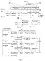
- FIG. 4shows the basic process flow for the DMA using the dependency according to an embodiment of the present invention.
- This figuredescribes the steps that the flash DMA and the IOC DMA take when using dependency.
- Steps 400 to 404describe the flash DMA part.
- Steps 405 to 409describe the IOC DMA part.
- the flash DMAreceives a descriptor with the dependency bit enabled.
- the descriptorcontains a dependency table index number.
- the dependency table index number in the flash DMA descriptorpoints to the corresponding dependency table entry that already has the “ready” status indicating that the said dependency table entry is already assigned to a particular flash descriptor and IOC descriptor pair.
- step 401the flash DMA updates the dependency table entry.
- the Flash DMAuses the dependency table index number to get the threshold in the dependency table.
- the thresholdis the end address of the flash DMA, and transferring the data corresponding to this address indicates that the flash DMA is already done.
- the flash DMAis also started and the dependency table entry status becomes “active”.
- step 402flash DMA is ongoing, and the flash DMA is monitoring for the ending address. In this step, the dependency table entry status is still “active”.
- step 403the flash DMA detects the matching end address and sets the dependency table entry status to “completed”.
- the flash DMAchecks that the dependency table entry already has the “initiated” status set.
- step 404is omitted.
- the second set of process stepsdiscusses the IOC DMA side dependency.
- the IOC DMAreceives a descriptor with the dependency bit enabled.
- IOC DMAuses the index number to locate the dependency table entry, and sees that the dependency table entry status is still not yet “completed”. In this step the dependency table entry status can either be “ready” or “active”.
- IOC DMAwait for the dependency table entry status to be become “completed”. Flash DMA's steps 400 , 401 , and 402 may occur in parallel with IOC DMA's steps 405 , 406 , and 407 .
- step 408IOC DMA detect that the dependency table entry status is already “completed” and starts the IOC data DMA.
- IOC DMAsets the dependency table entry status to “initiated”.
- the IOC DMAdirectly changes the status from “completed” to “free” and step 404 is omitted. The following steps occur in sequence: step 403 , then step 408 , then step 409 , and then step 404 .
- FIG. 5shows the basic process flow for the DMA using the dependency and snooping according to an embodiment of the present invention.
- This figuredescribes the steps that the flash DMA and the IOC DMA take when using dependency and snooping.
- Steps 500 to 504describe the flash DMA part.
- Steps 505 to 514describe the IOC DMA part.
- the process flow for dependency with snoopinghas similarities with the process flow for dependency only. The only part that changed is the process flow for the IOC DMA, since the IOC DMA side has the snooping function.
- the flash DMA process flowremains the same.
- Flash DMA steps 500 to 504is exactly the same as the flash DMA steps 400 to 404 in the previous figure.
- step 504is omitted.
- the second set of process stepsdiscusses the IOC DMA side dependency with snooping.
- the snooping feature of the IOC DMAcan be enabled via a register setting.
- the IOC DMAreceives a descriptor with the dependency bit enabled.
- the IOC DMAuses the index number and checks the dependency table entry status. If the dependency table entry status is “completed”, the flash DMA has already transferred the data to cache, and the IOC DMA can proceed with normal data transfer from the cache to the IOC. If the dependency table entry status is “active”, the flash DMA is still transferring data from the flash to the cache and the IOC DMA cannot proceed with the data transfer from cache to IOC since the data it needs is not yet completely in cache.
- the IOC DMAIf the dependency table entry status is already in “active” status, the IOC DMA also cannot begin bus snooping since there's a big possibility that the data it's trying to snoop was already transferred. In this case IOC DMA has no choice but to wait for the status to become “completed”. If the dependency table entry status is “free” or “ready”, the flash DMA has not yet begun transferring data to cache. For this case, IOC DMA has the option to snoop the flash DMA to cache bus, or to wait for the “completion” status and then continue with the normal DMA from cache to the IOC. In step 506 , existence of a snoop condition is seen since the dependency table entry status is still “free” or “ready”.
- step 507the IOC DMA starts snooping by tapping the flash DMA cache access request and cache transfer.
- step 508the IOC DMA has already caught the address of the start data in the flash DMA transfer to cache.
- IOC DMAis transferring the data (presented by the flash DMA to the cache) directly to the IOC.
- decision box 509IOC DMA monitors its buffer space. If there is still enough buffer space, the process goes to step 510 and the data from the snooping data is still being transferred to the IOC until all the needed data is done.
- the IOC DMABy the time the process goes to step 514 , the IOC DMA has already completed its DMA via snooping, and the IOC DMA simply waits for the dependency table entry status to become “completed” so it can set the status to “initiated” in step 514 , even though the actual IOC DMA transfer is already done. This is done so that the flash DMA, upon seeing the “initiated’ status, can set the status to “free” again so that the dependency table entry can be re-used for the next flash-cache-IOC transfer. If the buffer becomes full, the process goes to step 512 where the snooping is stopped.
- the IOC DMAreverts back to waiting for the dependency table entry to have a “completed” status. In this scenario, even if buffer space becomes available, snooping cannot be resumed since some flash to cache data were already bypassed during the flow control condition.
- the IOC DMAsees the “completed” status of the dependency table entry, and starts to resume the IOC DMA. This time the data comes from the cache (not from the snooping) and the data starting point begins from the point where the buffer became full.
- the processgoes to step 514 and sets the dependency table entry status to “initiated”.
- the IOC DMAdirectly changes the status from “completed” to “free”.
- FIG. 6shows a variation of the invention using data striping according to an embodiment of the present invention.
- Access to non-volatile memoryis relatively slower compared to high speed IO protocols.
- To speed up the non-volatile memory data transfer data stripingis used together with non-volatile memory multi-bank design.
- the parallel access to multi-bank non-volatile memory arraysmultiplies the bandwidth by the number of banks.
- the original data bufferis split into 4 data stripe buffers, namely stripe buffer A 605 , B 606 , C 607 , and D 608 .
- the 4 data stripe buffers and the corresponding non-volatile memory banks, namely bank A, bank B, bank C, and bank Dare handled concurrently by their respective DMA 1 engines, namely DMA 1 A 601 , DMA 1 B 602 , DMA 1 C 603 , and DMA 1 D 604 .
- the DMA engines and data stripe buffersare paired together by their respective data descriptors 600 . From the point of view of DMA 2 611 and its data descriptor 609 , it needs all the data from the non-volatile memory banks to be transferred to the corresponding data stripe buffers before DMA 2 611 can begin.
- the 4 DMA engines(DMA 1 A 601 , DMA 1 B 602 , DMA 1 C 603 , and DMA 1 D 604 ) concurrently process their respective non-volatile memory banks (bank A, bank B, bank C, and bank D) and corresponding data stripe buffers (data stripe buffers A 605 , B 606 , C 607 , and D 608 ). Due to resource arbitration and contention, any one of the transfers to the 4 data stripe buffers may finish first, and in this example, DMA 1 D 604 is the 1 st to finish transferring the corresponding data to data stripe buffer D 608 in cache.
- the threshold fieldcontains the address of the last data of the buffer.
- the compare with the threshold valueshould not trigger the setting of the “completed” status since the other data stripes are not yet fully transferred to their corresponding data stripe buffers in cache.
- a schememust ensure that all the data stripes of the various DMA engines are already fully transferred to cache before the “complete” status can be set.
- the scheme presented hereis the addition of a Range field 610 in the dependency table entry.
- the Range field 610tracks the end addresses of the data stripe buffers, and counts the number of data stripe buffers that's already done with the non-volatile memory to data stripe buffer transfer. Once the count reaches the total number of data stripe buffers indicated in the Range field 610 , the “complete” status can be set. More details about the Range field 610 are explained in FIG. 7 .
- FIG. 7illustrates the details of the Range field 700 according to an embodiment of the present invention.
- the Threshold field 701comprises a 32 bit value which is made up of a 16 bit Base HI 705 , an 8 bit Base Range 706 and a 8 bit Base LO 707 .
- the Range field 700contains information regarding the data stripe buffer size and location in the cache memory map and is made up of the Offset Select 702 , Minimum Range 703 , and the Maximum Range 704 .
- the Offset Select 702corresponds to data stripe size and determines how many bits are in the Base LO field and how many lower address bits are used to compare for the Base LO 707 value while the Minimum Range field and the Maximum Range field are fixed at 8 bit length.
- Minimum Range 703is added with the next 8 Threshold address bits Base Range 706 (for this example it's made up of Threshold address bits [15:8] based on an Offset Select of 8) to get the Minimum Address 708 (which is the ending middle [15:8] address bits of the first data stripe buffer).
- Maximum Range 704relates to the location of the last data stripe buffer in the cache memory map and determines the compare value for the ending address of the last data stripe buffer.
- Maximum Range 704is added with the next 8 Threshold address bits Base Range 706 to get the Maximum Address 709 (which is the ending middle [15:8] address bits of the last data stripe buffer).
- the remaining upper Threshold address bitsmake up the Base HI 705 address bits (for this example it's made up of Threshold address bits [31:16] based on an Offset Select of 8).
- the Minimum Range 703(appended with 1-bit binary zero value beyond its MSBit) is subtracted from the Maximum Range 704 (appended with 1-bit binary one value beyond its MSBit) to get the Difference 712 .
- the Count 710 valueis the number of data stripes present in the buffer.
- a data structureis used for coordinating dual channel DMA transfer wherein the data structure comprises a table comprising one or more entry, the one or more entry comprises a status initialized to be free and an index operable to be assigned to a first data descriptor and a second data descriptor if the status is free whereby a data buffer is accessed by a first and a second DMA engine according to the first and second data descriptor.
- the one or more entryfurther comprises a threshold; and the status is set to be ready upon a corresponding index being assigned and a value being assigned to a corresponding threshold.
- the first data descriptor and the second data descriptorare prepared by one or more CPU; wherein a first DMA engine transfers data from a source device to a data buffer according to the first data descriptor subsequent to the preparation completion thereof; wherein the status is set to be active upon the first DMA engine starting data transfer; wherein the status is set to be completed upon the first DMA engine data transfer reaching the threshold; wherein a second DMA engine transfers data from the data buffer to a destination device according to the second data descriptor upon the preparation completion thereof and the status being set to be completed; wherein the status is set to be initiated upon the second DMA engine starting data transfer; and wherein the status is set to be free upon the first DMA engine detecting the status being set to initiated whereby the initiated state is monitored for advanced notification of data transfer.
- the first data descriptor and the second data descriptorare prepared concurrently.
- the first and second DMA enginetransfer data from the source device to the destination device in response to the data structure without intervention from the one or more CPU subsequent to the first and second data descriptors preparation completion thereof.
- data buffercomprises one or more data stripe buffer; wherein one or more entry further comprises one or more range for tracking the end address of the one or more data stripe buffer and the number of data stripe buffer fully transferred.
- the one or more rangefurther comprises one or more offset select, one or more minimum range and one or more maximum range whereby size of the one or more data stripe buffer is determined and compare logic for generating completed status is reduced.
- data transfer to the one or more data stripe bufferis handled by one or more DMA engine.
- a data transfer methodcomprises the steps of: checking a data structure for an entry comprising a state set to be free; assigning an index of the entry to a first data descriptor and a second data descriptor; assigning a value to a threshold of the entry; setting the state to be ready upon assigning the threshold; preparing the first data descriptor and the second data descriptor by one or more CPU; transferring data from a source device to a data buffer using a first DMA engine according to the first data descriptor subsequent to the preparation completion thereof; setting the state to be active upon the first DMA engine starting data transfer; setting the state to be completed upon the first DMA engine data transfer reaching the threshold of the entry; transferring data from the data buffer to a destination device using a second DMA engine according to the second data descriptor upon the preparation completion thereof and the state being assigned to be completed; setting the state to be initiated upon the second DMA engine starting data transfer; and setting the state to be free upon the first DMA engine detecting the status
- the one or more CPUprepares the first data descriptor and the second data descriptor concurrently.
- the first and second DMA enginetransfer data from the source device to the destination device in response to the data structure without intervention from the one or more CPU subsequent to the first and second data descriptors preparation completion thereof.
- a data transfer methodcomprises the steps of: checking a data structure for an entry comprising a state set to be free; assigning an index of the entry to a first data descriptor and a second data descriptor; assigning a value to a threshold of the entry; setting the state to be ready upon assigning the threshold; preparing the first data descriptor and the second data descriptor by one or more CPU; transferring data from a source device to a data buffer using a first DMA engine according to the first data descriptor subsequent to the preparation completion thereof; monitoring an address bus for detecting a starting address of the first data descriptor; monitoring a data bus for detecting a first valid data of the first DMA engine; transferring one or more valid data of the first DMA engine to a destination device using a second DMA engine according to the second data descriptor upon detecting the first valid data of the first DMA engine; setting the state to be completed upon the first DMA engine data transfer reaching the threshold of the entry; setting the state to
- the second DMA engineis flow controlled for preventing a buffer overflow of the second DMA engine.
- the data transfer methodfurther comprises the steps of: Stopping the second DMA engine data transfer upon a buffer overflow; and transferring one or more data from the data buffer to the destination device using a second DMA engine according to the second data descriptor upon the first DMA engine data transfer reaching the threshold of the entry.
- a data transfer methodcomprises the steps of transferring data from a source device to a data buffer using a first DMA engine according to a first data descriptor prepared by one or more CPU; transferring data from the data buffer to a destination device using a second DMA engine according to a second data descriptor prepared by the one or more CPU; wherein the data buffer is accessed by the first and second DMA engine according to a data structure whereby data transfer is without CPU intervention subsequent to the first and second data descriptor being prepared by the one or more CPU.
- a data transfer methodcomprises the steps of checking a data structure for an entry comprising a state set to be free; assigning an index of the entry to a first data descriptor and a second data descriptor; assigning a value to a threshold of the entry; setting the state to be ready upon assigning the threshold; preparing the first data descriptor and the second data descriptor by one or more CPU; transferring data from a source device to a data buffer using a first DMA engine according to the first data descriptor subsequent to the preparation completion thereof; monitoring an address bus for detecting a starting address of the first data descriptor; monitoring a data bus for detecting a first valid data of the first DMA engine; transferring one or more valid data of the first DMA engine to a destination device using a second DMA engine according to the second data descriptor upon detecting the first valid data of the first DMA engine; setting the state to be completed upon the first DMA engine data transfer reaching the threshold of the entry; and setting the state to
Landscapes
- Engineering & Computer Science (AREA)
- Theoretical Computer Science (AREA)
- Physics & Mathematics (AREA)
- General Engineering & Computer Science (AREA)
- General Physics & Mathematics (AREA)
- Memory System Of A Hierarchy Structure (AREA)
Abstract
Description
Claims (13)
Priority Applications (1)
| Application Number | Priority Date | Filing Date | Title |
|---|---|---|---|
| US11/399,736US7620748B1 (en) | 2006-04-06 | 2006-04-06 | Hardware assisted non-volatile memory-to-input/output direct memory access (DMA) transfer |
Applications Claiming Priority (1)
| Application Number | Priority Date | Filing Date | Title |
|---|---|---|---|
| US11/399,736US7620748B1 (en) | 2006-04-06 | 2006-04-06 | Hardware assisted non-volatile memory-to-input/output direct memory access (DMA) transfer |
Publications (1)
| Publication Number | Publication Date |
|---|---|
| US7620748B1true US7620748B1 (en) | 2009-11-17 |
Family
ID=41279753
Family Applications (1)
| Application Number | Title | Priority Date | Filing Date |
|---|---|---|---|
| US11/399,736Active - Reinstated2026-07-03US7620748B1 (en) | 2006-04-06 | 2006-04-06 | Hardware assisted non-volatile memory-to-input/output direct memory access (DMA) transfer |
Country Status (1)
| Country | Link |
|---|---|
| US (1) | US7620748B1 (en) |
Cited By (45)
| Publication number | Priority date | Publication date | Assignee | Title |
|---|---|---|---|---|
| US20100169550A1 (en)* | 2008-12-27 | 2010-07-01 | Kabushiki Kaisha Toshiba | Semiconductor memory device, data transfer device, and method of controlling semiconductor memory device |
| CN101986287A (en)* | 2010-11-25 | 2011-03-16 | 中国人民解放军国防科学技术大学 | Reform buffer for vector data streams |
| US20110113186A1 (en)* | 2009-09-14 | 2011-05-12 | Bitmicro Networks, Inc. | Reducing erase cycles in an electronic storage device that uses at least one erase-limited memory device |
| US8165301B1 (en) | 2006-04-04 | 2012-04-24 | Bitmicro Networks, Inc. | Input-output device and storage controller handshake protocol using key exchange for data security |
| US8341311B1 (en)* | 2008-11-18 | 2012-12-25 | Entorian Technologies, Inc | System and method for reduced latency data transfers from flash memory to host by utilizing concurrent transfers into RAM buffer memory and FIFO host interface |
| US20140047058A1 (en)* | 2012-08-09 | 2014-02-13 | Spectra Logic Corporation | Direct memory access of remote data |
| US8788725B2 (en) | 2009-09-07 | 2014-07-22 | Bitmicro Networks, Inc. | Multilevel memory bus system for solid-state mass storage |
| US8959307B1 (en) | 2007-11-16 | 2015-02-17 | Bitmicro Networks, Inc. | Reduced latency memory read transactions in storage devices |
| US20150143031A1 (en)* | 2012-05-12 | 2015-05-21 | Memblaze Technology (Beijing) Co., Ltd. | Method for writing data into storage device and storage device |
| US9043669B1 (en) | 2012-05-18 | 2015-05-26 | Bitmicro Networks, Inc. | Distributed ECC engine for storage media |
| US9135190B1 (en) | 2009-09-04 | 2015-09-15 | Bitmicro Networks, Inc. | Multi-profile memory controller for computing devices |
| US9372755B1 (en) | 2011-10-05 | 2016-06-21 | Bitmicro Networks, Inc. | Adaptive power cycle sequences for data recovery |
| US9400617B2 (en) | 2013-03-15 | 2016-07-26 | Bitmicro Networks, Inc. | Hardware-assisted DMA transfer with dependency table configured to permit-in parallel-data drain from cache without processor intervention when filled or drained |
| US9423457B2 (en) | 2013-03-14 | 2016-08-23 | Bitmicro Networks, Inc. | Self-test solution for delay locked loops |
| US9430386B2 (en) | 2013-03-15 | 2016-08-30 | Bitmicro Networks, Inc. | Multi-leveled cache management in a hybrid storage system |
| US20160283415A1 (en)* | 2015-03-27 | 2016-09-29 | Chad McBride | Direct memory access descriptor processing |
| US9501436B1 (en) | 2013-03-15 | 2016-11-22 | Bitmicro Networks, Inc. | Multi-level message passing descriptor |
| CN106170757A (en)* | 2014-11-29 | 2016-11-30 | 华为技术有限公司 | A kind of date storage method and device |
| US9672178B1 (en) | 2013-03-15 | 2017-06-06 | Bitmicro Networks, Inc. | Bit-mapped DMA transfer with dependency table configured to monitor status so that a processor is not rendered as a bottleneck in a system |
| US9720603B1 (en) | 2013-03-15 | 2017-08-01 | Bitmicro Networks, Inc. | IOC to IOC distributed caching architecture |
| US9734067B1 (en) | 2013-03-15 | 2017-08-15 | Bitmicro Networks, Inc. | Write buffering |
| US9798688B1 (en) | 2013-03-15 | 2017-10-24 | Bitmicro Networks, Inc. | Bus arbitration with routing and failover mechanism |
| US9811461B1 (en) | 2014-04-17 | 2017-11-07 | Bitmicro Networks, Inc. | Data storage system |
| US9842024B1 (en) | 2013-03-15 | 2017-12-12 | Bitmicro Networks, Inc. | Flash electronic disk with RAID controller |
| US9858084B2 (en) | 2013-03-15 | 2018-01-02 | Bitmicro Networks, Inc. | Copying of power-on reset sequencer descriptor from nonvolatile memory to random access memory |
| US9875205B1 (en) | 2013-03-15 | 2018-01-23 | Bitmicro Networks, Inc. | Network of memory systems |
| US9916213B1 (en) | 2013-03-15 | 2018-03-13 | Bitmicro Networks, Inc. | Bus arbitration with routing and failover mechanism |
| US9934045B1 (en) | 2013-03-15 | 2018-04-03 | Bitmicro Networks, Inc. | Embedded system boot from a storage device |
| US9952991B1 (en) | 2014-04-17 | 2018-04-24 | Bitmicro Networks, Inc. | Systematic method on queuing of descriptors for multiple flash intelligent DMA engine operation |
| US9971524B1 (en) | 2013-03-15 | 2018-05-15 | Bitmicro Networks, Inc. | Scatter-gather approach for parallel data transfer in a mass storage system |
| US10025736B1 (en) | 2014-04-17 | 2018-07-17 | Bitmicro Networks, Inc. | Exchange message protocol message transmission between two devices |
| US10042792B1 (en) | 2014-04-17 | 2018-08-07 | Bitmicro Networks, Inc. | Method for transferring and receiving frames across PCI express bus for SSD device |
| US10055150B1 (en) | 2014-04-17 | 2018-08-21 | Bitmicro Networks, Inc. | Writing volatile scattered memory metadata to flash device |
| US10078604B1 (en) | 2014-04-17 | 2018-09-18 | Bitmicro Networks, Inc. | Interrupt coalescing |
| CN108572798A (en)* | 2017-03-10 | 2018-09-25 | 三星电子株式会社 | Storage device and method for performing snooping operation for fast data transmission |
| US10149399B1 (en) | 2009-09-04 | 2018-12-04 | Bitmicro Llc | Solid state drive with improved enclosure assembly |
| CN110399321A (en)* | 2018-04-25 | 2019-11-01 | 爱思开海力士有限公司 | Storage system and method of operation |
| WO2019217064A1 (en)* | 2018-05-09 | 2019-11-14 | Micron Technology, Inc. | Latency indication in memory system or sub-system |
| US10489318B1 (en) | 2013-03-15 | 2019-11-26 | Bitmicro Networks, Inc. | Scatter-gather approach for parallel data transfer in a mass storage system |
| US10552050B1 (en) | 2017-04-07 | 2020-02-04 | Bitmicro Llc | Multi-dimensional computer storage system |
| US10649687B2 (en) | 2018-05-09 | 2020-05-12 | Micron Technology, Inc. | Memory buffer management and bypass |
| US20210014177A1 (en)* | 2020-09-26 | 2021-01-14 | Intel Corporation | Deterministic packet scheduling and dma for time sensitive networking |
| US10942854B2 (en) | 2018-05-09 | 2021-03-09 | Micron Technology, Inc. | Prefetch management for memory |
| US11003388B2 (en) | 2018-05-09 | 2021-05-11 | Microon Technology, Inc. | Prefetch signaling in memory system or sub system |
| US11099966B2 (en)* | 2020-01-09 | 2021-08-24 | International Business Machines Corporation | Efficient generation of instrumentation data for direct memory access operations |
Citations (6)
| Publication number | Priority date | Publication date | Assignee | Title |
|---|---|---|---|---|
| US5644784A (en)* | 1995-03-03 | 1997-07-01 | Intel Corporation | Linear list based DMA control structure |
| US5822251A (en)* | 1997-08-25 | 1998-10-13 | Bit Microsystems, Inc. | Expandable flash-memory mass-storage using shared buddy lines and intermediate flash-bus between device-specific buffers and flash-intelligent DMA controllers |
| US5881264A (en)* | 1996-01-31 | 1999-03-09 | Kabushiki Kaisha Toshiba | Memory controller and memory control system |
| US5918033A (en)* | 1997-01-08 | 1999-06-29 | Intel Corporation | Method and apparatus for dynamic location and control of processor resources to increase resolution of data dependency stalls |
| US6557095B1 (en)* | 1999-12-27 | 2003-04-29 | Intel Corporation | Scheduling operations using a dependency matrix |
| US20070174493A1 (en)* | 2006-01-26 | 2007-07-26 | International Business Machines Corporation | Method and apparatus for tracking command order dependencies |
- 2006
- 2006-04-06USUS11/399,736patent/US7620748B1/enactiveActive - Reinstated
Patent Citations (6)
| Publication number | Priority date | Publication date | Assignee | Title |
|---|---|---|---|---|
| US5644784A (en)* | 1995-03-03 | 1997-07-01 | Intel Corporation | Linear list based DMA control structure |
| US5881264A (en)* | 1996-01-31 | 1999-03-09 | Kabushiki Kaisha Toshiba | Memory controller and memory control system |
| US5918033A (en)* | 1997-01-08 | 1999-06-29 | Intel Corporation | Method and apparatus for dynamic location and control of processor resources to increase resolution of data dependency stalls |
| US5822251A (en)* | 1997-08-25 | 1998-10-13 | Bit Microsystems, Inc. | Expandable flash-memory mass-storage using shared buddy lines and intermediate flash-bus between device-specific buffers and flash-intelligent DMA controllers |
| US6557095B1 (en)* | 1999-12-27 | 2003-04-29 | Intel Corporation | Scheduling operations using a dependency matrix |
| US20070174493A1 (en)* | 2006-01-26 | 2007-07-26 | International Business Machines Corporation | Method and apparatus for tracking command order dependencies |
Cited By (88)
| Publication number | Priority date | Publication date | Assignee | Title |
|---|---|---|---|---|
| US8165301B1 (en) | 2006-04-04 | 2012-04-24 | Bitmicro Networks, Inc. | Input-output device and storage controller handshake protocol using key exchange for data security |
| US8959307B1 (en) | 2007-11-16 | 2015-02-17 | Bitmicro Networks, Inc. | Reduced latency memory read transactions in storage devices |
| US10120586B1 (en) | 2007-11-16 | 2018-11-06 | Bitmicro, Llc | Memory transaction with reduced latency |
| US8341311B1 (en)* | 2008-11-18 | 2012-12-25 | Entorian Technologies, Inc | System and method for reduced latency data transfers from flash memory to host by utilizing concurrent transfers into RAM buffer memory and FIFO host interface |
| US20100169550A1 (en)* | 2008-12-27 | 2010-07-01 | Kabushiki Kaisha Toshiba | Semiconductor memory device, data transfer device, and method of controlling semiconductor memory device |
| US10149399B1 (en) | 2009-09-04 | 2018-12-04 | Bitmicro Llc | Solid state drive with improved enclosure assembly |
| US9135190B1 (en) | 2009-09-04 | 2015-09-15 | Bitmicro Networks, Inc. | Multi-profile memory controller for computing devices |
| US10133686B2 (en) | 2009-09-07 | 2018-11-20 | Bitmicro Llc | Multilevel memory bus system |
| US8788725B2 (en) | 2009-09-07 | 2014-07-22 | Bitmicro Networks, Inc. | Multilevel memory bus system for solid-state mass storage |
| US8560804B2 (en) | 2009-09-14 | 2013-10-15 | Bitmicro Networks, Inc. | Reducing erase cycles in an electronic storage device that uses at least one erase-limited memory device |
| US9484103B1 (en)* | 2009-09-14 | 2016-11-01 | Bitmicro Networks, Inc. | Electronic storage device |
| US20110113186A1 (en)* | 2009-09-14 | 2011-05-12 | Bitmicro Networks, Inc. | Reducing erase cycles in an electronic storage device that uses at least one erase-limited memory device |
| US9099187B2 (en)* | 2009-09-14 | 2015-08-04 | Bitmicro Networks, Inc. | Reducing erase cycles in an electronic storage device that uses at least one erase-limited memory device |
| US10082966B1 (en) | 2009-09-14 | 2018-09-25 | Bitmicro Llc | Electronic storage device |
| CN101986287B (en)* | 2010-11-25 | 2012-10-17 | 中国人民解放军国防科学技术大学 | Rearranging buffers for vector data streams |
| CN101986287A (en)* | 2010-11-25 | 2011-03-16 | 中国人民解放军国防科学技术大学 | Reform buffer for vector data streams |
| US10180887B1 (en) | 2011-10-05 | 2019-01-15 | Bitmicro Llc | Adaptive power cycle sequences for data recovery |
| US9372755B1 (en) | 2011-10-05 | 2016-06-21 | Bitmicro Networks, Inc. | Adaptive power cycle sequences for data recovery |
| US9395921B2 (en)* | 2012-05-12 | 2016-07-19 | Memblaze Technology (Beijing) Co., Ltd. | Writing data using DMA by specifying a buffer address and a flash memory address |
| US20150143031A1 (en)* | 2012-05-12 | 2015-05-21 | Memblaze Technology (Beijing) Co., Ltd. | Method for writing data into storage device and storage device |
| US9996419B1 (en) | 2012-05-18 | 2018-06-12 | Bitmicro Llc | Storage system with distributed ECC capability |
| US9043669B1 (en) | 2012-05-18 | 2015-05-26 | Bitmicro Networks, Inc. | Distributed ECC engine for storage media |
| US20140047058A1 (en)* | 2012-08-09 | 2014-02-13 | Spectra Logic Corporation | Direct memory access of remote data |
| US9645738B2 (en)* | 2012-08-09 | 2017-05-09 | Spectra Logic Corporation | Direct memory access of remote data |
| US9423457B2 (en) | 2013-03-14 | 2016-08-23 | Bitmicro Networks, Inc. | Self-test solution for delay locked loops |
| US9977077B1 (en) | 2013-03-14 | 2018-05-22 | Bitmicro Llc | Self-test solution for delay locked loops |
| US10423554B1 (en) | 2013-03-15 | 2019-09-24 | Bitmicro Networks, Inc | Bus arbitration with routing and failover mechanism |
| US9734067B1 (en) | 2013-03-15 | 2017-08-15 | Bitmicro Networks, Inc. | Write buffering |
| US9798688B1 (en) | 2013-03-15 | 2017-10-24 | Bitmicro Networks, Inc. | Bus arbitration with routing and failover mechanism |
| US9720603B1 (en) | 2013-03-15 | 2017-08-01 | Bitmicro Networks, Inc. | IOC to IOC distributed caching architecture |
| US10210084B1 (en) | 2013-03-15 | 2019-02-19 | Bitmicro Llc | Multi-leveled cache management in a hybrid storage system |
| US9842024B1 (en) | 2013-03-15 | 2017-12-12 | Bitmicro Networks, Inc. | Flash electronic disk with RAID controller |
| US9858084B2 (en) | 2013-03-15 | 2018-01-02 | Bitmicro Networks, Inc. | Copying of power-on reset sequencer descriptor from nonvolatile memory to random access memory |
| US9875205B1 (en) | 2013-03-15 | 2018-01-23 | Bitmicro Networks, Inc. | Network of memory systems |
| US9916213B1 (en) | 2013-03-15 | 2018-03-13 | Bitmicro Networks, Inc. | Bus arbitration with routing and failover mechanism |
| US9934045B1 (en) | 2013-03-15 | 2018-04-03 | Bitmicro Networks, Inc. | Embedded system boot from a storage device |
| US9934160B1 (en)* | 2013-03-15 | 2018-04-03 | Bitmicro Llc | Bit-mapped DMA and IOC transfer with dependency table comprising plurality of index fields in the cache for DMA transfer |
| US9672178B1 (en) | 2013-03-15 | 2017-06-06 | Bitmicro Networks, Inc. | Bit-mapped DMA transfer with dependency table configured to monitor status so that a processor is not rendered as a bottleneck in a system |
| US9971524B1 (en) | 2013-03-15 | 2018-05-15 | Bitmicro Networks, Inc. | Scatter-gather approach for parallel data transfer in a mass storage system |
| US9501436B1 (en) | 2013-03-15 | 2016-11-22 | Bitmicro Networks, Inc. | Multi-level message passing descriptor |
| US10489318B1 (en) | 2013-03-15 | 2019-11-26 | Bitmicro Networks, Inc. | Scatter-gather approach for parallel data transfer in a mass storage system |
| US10013373B1 (en) | 2013-03-15 | 2018-07-03 | Bitmicro Networks, Inc. | Multi-level message passing descriptor |
| US10120694B2 (en) | 2013-03-15 | 2018-11-06 | Bitmicro Networks, Inc. | Embedded system boot from a storage device |
| US10042799B1 (en) | 2013-03-15 | 2018-08-07 | Bitmicro, Llc | Bit-mapped DMA transfer with dependency table configured to monitor status so that a processor is not rendered as a bottleneck in a system |
| US9430386B2 (en) | 2013-03-15 | 2016-08-30 | Bitmicro Networks, Inc. | Multi-leveled cache management in a hybrid storage system |
| US9400617B2 (en) | 2013-03-15 | 2016-07-26 | Bitmicro Networks, Inc. | Hardware-assisted DMA transfer with dependency table configured to permit-in parallel-data drain from cache without processor intervention when filled or drained |
| US10042792B1 (en) | 2014-04-17 | 2018-08-07 | Bitmicro Networks, Inc. | Method for transferring and receiving frames across PCI express bus for SSD device |
| US9811461B1 (en) | 2014-04-17 | 2017-11-07 | Bitmicro Networks, Inc. | Data storage system |
| US10078604B1 (en) | 2014-04-17 | 2018-09-18 | Bitmicro Networks, Inc. | Interrupt coalescing |
| US10055150B1 (en) | 2014-04-17 | 2018-08-21 | Bitmicro Networks, Inc. | Writing volatile scattered memory metadata to flash device |
| US10025736B1 (en) | 2014-04-17 | 2018-07-17 | Bitmicro Networks, Inc. | Exchange message protocol message transmission between two devices |
| US9952991B1 (en) | 2014-04-17 | 2018-04-24 | Bitmicro Networks, Inc. | Systematic method on queuing of descriptors for multiple flash intelligent DMA engine operation |
| CN106170757B (en)* | 2014-11-29 | 2019-06-18 | 华为技术有限公司 | A data storage method and device |
| CN106170757A (en)* | 2014-11-29 | 2016-11-30 | 华为技术有限公司 | A kind of date storage method and device |
| CN107430566A (en)* | 2015-03-27 | 2017-12-01 | 微软技术许可有限责任公司 | The processing of direct memory access descriptor |
| US20160283415A1 (en)* | 2015-03-27 | 2016-09-29 | Chad McBride | Direct memory access descriptor processing |
| US9715464B2 (en)* | 2015-03-27 | 2017-07-25 | Microsoft Technology Licensing, Llc | Direct memory access descriptor processing |
| CN107430566B (en)* | 2015-03-27 | 2020-06-12 | 微软技术许可有限责任公司 | Direct memory access descriptor handling |
| US10572401B2 (en) | 2015-03-27 | 2020-02-25 | Microsoft Technology Licensing, Llc | Direct memory access descriptor processing using timestamps |
| US10528494B2 (en) | 2015-03-27 | 2020-01-07 | Microsoft Technology Licensing, Llc | Direct memory access (“DMA”) descriptor processing using identifiers assigned to descriptors on DMA engines |
| US10459854B2 (en) | 2017-03-10 | 2019-10-29 | Samsung Electronics Co., Ltd. | Storage device including a snooper that monitors a system bus to detect completion of writing data to a buffer memory and a method thereof |
| US20200050559A1 (en)* | 2017-03-10 | 2020-02-13 | Samsung Electronics Co., Ltd. | Storage device performing a snooping operation for fast data transmission and a method thereof |
| US11016912B2 (en) | 2017-03-10 | 2021-05-25 | Samsung Electronics Co.,, Ltd. | Storage device or memory controller with first direct memory access engine configured to control writing first data into buffer memory and second direct memory access engine configured to control transmitting written first data to external host device |
| CN108572798A (en)* | 2017-03-10 | 2018-09-25 | 三星电子株式会社 | Storage device and method for performing snooping operation for fast data transmission |
| US10552050B1 (en) | 2017-04-07 | 2020-02-04 | Bitmicro Llc | Multi-dimensional computer storage system |
| US11645010B2 (en)* | 2018-04-25 | 2023-05-09 | SK Hynix Inc. | Solid state drive (SSD) memory system improving the speed of a read operation using parallel DMA data transfers |
| CN110399321A (en)* | 2018-04-25 | 2019-11-01 | 爱思开海力士有限公司 | Storage system and method of operation |
| US20210326075A1 (en)* | 2018-04-25 | 2021-10-21 | SK Hynix Inc. | Solid state drive (ssd) memory system improving the speed of a read operation using parallel dma data transfers |
| US10714159B2 (en) | 2018-05-09 | 2020-07-14 | Micron Technology, Inc. | Indication in memory system or sub-system of latency associated with performing an access command |
| US11604606B2 (en) | 2018-05-09 | 2023-03-14 | Micron Technology, Inc. | Prefetch signaling in memory system or subsystem |
| US12347521B2 (en) | 2018-05-09 | 2025-07-01 | Lodestar Licensing Group Llc | Time delay indication for host in memory system |
| CN112262365A (en)* | 2018-05-09 | 2021-01-22 | 美光科技公司 | Latency indication in a memory system or subsystem |
| US10942854B2 (en) | 2018-05-09 | 2021-03-09 | Micron Technology, Inc. | Prefetch management for memory |
| US10956333B2 (en) | 2018-05-09 | 2021-03-23 | Micron Technology, Inc. | Prefetching data based on data transfer within a memory system |
| US11003388B2 (en) | 2018-05-09 | 2021-05-11 | Microon Technology, Inc. | Prefetch signaling in memory system or sub system |
| US11010092B2 (en) | 2018-05-09 | 2021-05-18 | Micron Technology, Inc. | Prefetch signaling in memory system or sub-system |
| US10754578B2 (en) | 2018-05-09 | 2020-08-25 | Micron Technology, Inc. | Memory buffer management and bypass |
| CN112262365B (en)* | 2018-05-09 | 2024-05-24 | 美光科技公司 | Indication of latency in a memory system or subsystem |
| US10649687B2 (en) | 2018-05-09 | 2020-05-12 | Micron Technology, Inc. | Memory buffer management and bypass |
| US11340830B2 (en) | 2018-05-09 | 2022-05-24 | Micron Technology, Inc. | Memory buffer management and bypass |
| US11355169B2 (en) | 2018-05-09 | 2022-06-07 | Micron Technology, Inc. | Indicating latency associated with a memory request in a system |
| US10839874B2 (en) | 2018-05-09 | 2020-11-17 | Micron Technology, Inc. | Indicating latency associated with a memory request in a system |
| WO2019217064A1 (en)* | 2018-05-09 | 2019-11-14 | Micron Technology, Inc. | Latency indication in memory system or sub-system |
| US11822477B2 (en) | 2018-05-09 | 2023-11-21 | Micron Technology, Inc. | Prefetch management for memory |
| US11915788B2 (en) | 2018-05-09 | 2024-02-27 | Micron Technology, Inc. | Indication in memory system or sub-system of latency associated with performing an access command |
| US11099966B2 (en)* | 2020-01-09 | 2021-08-24 | International Business Machines Corporation | Efficient generation of instrumentation data for direct memory access operations |
| US12250163B2 (en)* | 2020-09-26 | 2025-03-11 | Intel Corporation | Deterministic packet scheduling and DMA for time sensitive networking |
| US20210014177A1 (en)* | 2020-09-26 | 2021-01-14 | Intel Corporation | Deterministic packet scheduling and dma for time sensitive networking |
Similar Documents
| Publication | Publication Date | Title |
|---|---|---|
| US7620748B1 (en) | Hardware assisted non-volatile memory-to-input/output direct memory access (DMA) transfer | |
| US6772237B2 (en) | Host controller interface descriptor fetching unit | |
| US9037810B2 (en) | Pre-fetching of data packets | |
| JP7340326B2 (en) | Perform maintenance operations | |
| JP2019067417A (en) | Final level cache system and corresponding method | |
| US20220147404A1 (en) | Method And Apparatus For Accessing Critical Resource, Computer Device, And Readable Storage Medium | |
| US9632958B2 (en) | System for migrating stash transactions | |
| US7543124B1 (en) | Method for preventing page replacement of unreferenced read-ahead file pages | |
| US8996818B2 (en) | Bypassing memory requests to a main memory | |
| US7117338B2 (en) | Virtual memory address translation control by TLB purge monitoring | |
| JP7572279B2 (en) | STORAGE DEVICE FOR MANAGING COMMANDS HAVING OVERLAP RANGE AND METHOD FOR CHECKING OVERLAP - Patent application | |
| US8639840B2 (en) | Processing unit, chip, computing device and method for accelerating data transmission | |
| CN110781107B (en) | Low-delay fusion IO control method and device based on DRAM interface | |
| WO2025113289A1 (en) | Data transmission method and apparatus, accelerator device, and host | |
| US10042773B2 (en) | Advance cache allocator | |
| CN100378656C (en) | Integrated circuit with non-volatile memory and method for fetching data from said memory | |
| WO2024036985A1 (en) | Storage system, computational storage processor and solid-state drive thereof, and data reading method and data writing method therefor | |
| US8671232B1 (en) | System and method for dynamically migrating stash transactions | |
| JP2005536798A (en) | Processor prefetching that matches the memory bus protocol characteristics | |
| US9015272B2 (en) | Microcomputer | |
| US8850159B2 (en) | Method and system for latency optimized ATS usage | |
| CN108052296B (en) | Data reading method and device and computer storage medium | |
| US8452920B1 (en) | System and method for controlling a dynamic random access memory | |
| US20080209085A1 (en) | Semiconductor device and dma transfer method | |
| US7120758B2 (en) | Technique for improving processor performance |
Legal Events
| Date | Code | Title | Description |
|---|---|---|---|
| AS | Assignment | Owner name:BITMICRO NETWORKS, CALIFORNIA Free format text:ASSIGNMENT OF ASSIGNORS INTEREST;ASSIGNORS:BRUCE, RICARDO;BRUCE, REY;ZALZOS SAMBILAY JR., FEDERICO;AND OTHERS;REEL/FRAME:017771/0620 Effective date:20060406 | |
| REMI | Maintenance fee reminder mailed | ||
| LAPS | Lapse for failure to pay maintenance fees | ||
| REIN | Reinstatement after maintenance fee payment confirmed | ||
| FEPP | Fee payment procedure | Free format text:PETITION RELATED TO MAINTENANCE FEES FILED (ORIGINAL EVENT CODE: PMFP); ENTITY STATUS OF PATENT OWNER: LARGE ENTITY | |
| FEPP | Fee payment procedure | Free format text:PETITION RELATED TO MAINTENANCE FEES GRANTED (ORIGINAL EVENT CODE: PMFG); ENTITY STATUS OF PATENT OWNER: LARGE ENTITY | |
| FP | Lapsed due to failure to pay maintenance fee | Effective date:20131117 | |
| FPAY | Fee payment | Year of fee payment:4 | |
| SULP | Surcharge for late payment | ||
| PRDP | Patent reinstated due to the acceptance of a late maintenance fee | Effective date:20140411 | |
| STCF | Information on status: patent grant | Free format text:PATENTED CASE | |
| FEPP | Fee payment procedure | Free format text:PAT HOLDER NO LONGER CLAIMS SMALL ENTITY STATUS, ENTITY STATUS SET TO UNDISCOUNTED (ORIGINAL EVENT CODE: STOL); ENTITY STATUS OF PATENT OWNER: LARGE ENTITY | |
| FPAY | Fee payment | Year of fee payment:8 | |
| AS | Assignment | Owner name:BITMICRO LLC, SOUTH CAROLINA Free format text:ASSIGNMENT OF ASSIGNORS INTEREST;ASSIGNOR:BITMICRO NETWORKS, INC.;REEL/FRAME:043536/0407 Effective date:20170630 | |
| FEPP | Fee payment procedure | Free format text:MAINTENANCE FEE REMINDER MAILED (ORIGINAL EVENT CODE: REM.); ENTITY STATUS OF PATENT OWNER: LARGE ENTITY | |
| FEPP | Fee payment procedure | Free format text:11.5 YR SURCHARGE- LATE PMT W/IN 6 MO, LARGE ENTITY (ORIGINAL EVENT CODE: M1556); ENTITY STATUS OF PATENT OWNER: LARGE ENTITY | |
| MAFP | Maintenance fee payment | Free format text:PAYMENT OF MAINTENANCE FEE, 12TH YEAR, LARGE ENTITY (ORIGINAL EVENT CODE: M1553); ENTITY STATUS OF PATENT OWNER: LARGE ENTITY Year of fee payment:12 |