US7619739B1 - Detection and identification of biological agents using Bragg filters - Google Patents
Detection and identification of biological agents using Bragg filtersDownload PDFInfo
- Publication number
- US7619739B1 US7619739B1US10/614,188US61418803AUS7619739B1US 7619739 B1US7619739 B1US 7619739B1US 61418803 AUS61418803 AUS 61418803AUS 7619739 B1US7619739 B1US 7619739B1
- Authority
- US
- United States
- Prior art keywords
- sample
- grating
- optical
- optical grating
- filter
- Prior art date
- Legal status (The legal status is an assumption and is not a legal conclusion. Google has not performed a legal analysis and makes no representation as to the accuracy of the status listed.)
- Expired - Fee Related, expires
Links
Images


Classifications
- G—PHYSICS
- G01—MEASURING; TESTING
- G01N—INVESTIGATING OR ANALYSING MATERIALS BY DETERMINING THEIR CHEMICAL OR PHYSICAL PROPERTIES
- G01N33/00—Investigating or analysing materials by specific methods not covered by groups G01N1/00 - G01N31/00
- G01N33/48—Biological material, e.g. blood, urine; Haemocytometers
- G01N33/50—Chemical analysis of biological material, e.g. blood, urine; Testing involving biospecific ligand binding methods; Immunological testing
- G01N33/53—Immunoassay; Biospecific binding assay; Materials therefor
- G01N33/543—Immunoassay; Biospecific binding assay; Materials therefor with an insoluble carrier for immobilising immunochemicals
- G01N33/54366—Apparatus specially adapted for solid-phase testing
- G—PHYSICS
- G01—MEASURING; TESTING
- G01N—INVESTIGATING OR ANALYSING MATERIALS BY DETERMINING THEIR CHEMICAL OR PHYSICAL PROPERTIES
- G01N21/00—Investigating or analysing materials by the use of optical means, i.e. using sub-millimetre waves, infrared, visible or ultraviolet light
- G01N21/75—Systems in which material is subjected to a chemical reaction, the progress or the result of the reaction being investigated
- G01N21/77—Systems in which material is subjected to a chemical reaction, the progress or the result of the reaction being investigated by observing the effect on a chemical indicator
- G01N21/7703—Systems in which material is subjected to a chemical reaction, the progress or the result of the reaction being investigated by observing the effect on a chemical indicator using reagent-clad optical fibres or optical waveguides
- G01N21/774—Systems in which material is subjected to a chemical reaction, the progress or the result of the reaction being investigated by observing the effect on a chemical indicator using reagent-clad optical fibres or optical waveguides the reagent being on a grating or periodic structure
- G—PHYSICS
- G03—PHOTOGRAPHY; CINEMATOGRAPHY; ANALOGOUS TECHNIQUES USING WAVES OTHER THAN OPTICAL WAVES; ELECTROGRAPHY; HOLOGRAPHY
- G03H—HOLOGRAPHIC PROCESSES OR APPARATUS
- G03H1/00—Holographic processes or apparatus using light, infrared or ultraviolet waves for obtaining holograms or for obtaining an image from them; Details peculiar thereto
- G03H1/02—Details of features involved during the holographic process; Replication of holograms without interference recording
- G03H2001/026—Recording materials or recording processes
- G03H2001/0264—Organic recording material
- G—PHYSICS
- G03—PHOTOGRAPHY; CINEMATOGRAPHY; ANALOGOUS TECHNIQUES USING WAVES OTHER THAN OPTICAL WAVES; ELECTROGRAPHY; HOLOGRAPHY
- G03H—HOLOGRAPHIC PROCESSES OR APPARATUS
- G03H2250/00—Laminate comprising a hologram layer
- G03H2250/38—Liquid crystal
Definitions
- the present inventionrelates generally to a sensor system, and more specifically to a sensor for detecting biological and chemical agents in the environment.
- Antibody-based detection systemsare the most mature and advanced technology for biological agent detection and identification.
- Antibodiesare defined as any of the body immunoglobulins that are produced in response to specific antigens and that counteract their effects by neutralizing toxins, agglutinating bacteria or cells, and precipitating soluble antigens.
- Antigensare defined as protein or carbohydrate substances capable of stimulating an immune response.
- Antibodiesare very specific and bind only to their target, even in the presence of other material.
- antibodiesare normally immobilized on a substrate, e.g., a polymer, such as polyvinylethylene, polyethylene, or polystyrene, for subsequent incubation with the target organism or molecule.
- the antibodiesare not chemically bound to the substrate, but merely attached by hydrogen bonding or electrostatic charge.
- the antibody and antigenbind upon contact, thereby immobilizing the antigen.
- a second antibody to the target agentincubates, as well as binds to the antigen.
- This second antibodyis generally linked to some type of reporter system, usually an enzyme.
- the varying forms of these reporter systemsinclude, e.g., fluorescent, magnetic, enzymatic, calorimetric, etc. This transducer provides the means of detecting the presence of the antigen of interest.
- Enzyme linked immunosorbent assay(ELISA) is based on this process.
- An analyte in the antibody-antigen detection systemis typically in an aqueous solution or other liquid solution.
- the aqueous solutionmust make frequent and intimate contact with the immobilized antibody on the substrate material.
- a large surface area on the substrateallows a higher density of antibodies and hence a higher sensitivity.
- the antibodiesmust be tightly bound to the substrate to survive repeated motion of the analyte over the substrate without becoming detached and flushed away with the solution. Therefore, covalent bonding, rather than hydrogen bonding or electrostatic bonding, of the antibodies to the substrate is preferential.
- Many biological compounds of interest in the systemare proteins, e.g., enzymes, hormones, toxins, antibodies, and antigens. Proteins are composed of amino acids, having both an amino group (NH 2 ) and a carboxylic acid group (COOH). A substrate functionalized with one or both of these groups can be activated to chemically bind antibodies.
- the introduction of a second antibody in the ELISA processcomplicates and slows down the detection/identification process.
- a physical property change produced by the antibody-antigen chemical reactionprovides the basis for a more direct transduction mechanism.
- the transduction mechanism in an optics-based detection systemis based on a change in absorption or index of refraction, which is monitored by the optical system.
- detectorsare based on a change of index of refraction.
- One such sensoris based on surface plasmon resonance.
- Surface plasmon techniquesare difficult to integrate for multiplexed operation where multiple target agents can be monitored simultaneously. Also, their sensitivity cannot be engineered by sharpening the spectral or angular response to light.
- porous silicone.g., silicon
- optical interferometric sensore.g., interferometric sensor
- Interference filterscan be made with porous silicon.
- porous silicon interference filtersare incompatible with polymer waveguide technology and hence cannot be readily integrated onto a polymer waveguide chip.
- porous polymersare easier to apodize, i.e., sharpen, their spectral response using holographic techniques.
- polymer chemistryis more adaptable to functionalization with chemical groups for binding antibodies and antigens.
- Most immunosorbent assaysare conducted on polymer substrates.
- Porous siliconhas not been widely used for this application. No conventional methods propose the simultaneous use of porous semiconductors as both chemical and optical filters.
- Another known sensoris a doubly-differential interferometer-based sensor with evanescent wave surface detection.
- This sensoris a surface detector only and cannot take advantage of the extended surface area of a porous polymer. Furthermore, the sensor also requires polarized light and a modulator. Additionally, this sensor is a part of a system that does not provide for continuously monitoring the environment.
- the interferometeris also not flexible for sharpening the optical response for higher sensitivity.
- a conventional hologram-containing sensorconsists of a holographic grating recorded preferably in a gelatin, where reaction of chemical agents with the gelatin produces some change in the physical properties of the hologram matrix, thereby changing the diffraction properties of the hologram.
- a matrix containing a gratingserves to uptake an analyte, but does not allow for the analyte to flow through the system. Once the system is swollen, the only mechanism for replacing it with new samples is to remove the grating from the system and dry it out. Since the materials used are not porous, the system cannot take advantage of increased surface area to volume ratio and does not provide a convenient method for chemically filtering the analyte. These methods are also not compatible with waveguides for integration onto a chip.
- Another chemical and biochemical sensorincludes a planar waveguide with a grating coupler.
- a recognition layer containing specific chemical or biochemical binding partners, e.g., antibodies or antigens,is located on the waveguide.
- a chemical reaction on the recognition layerchanges the effective refractive index of the guiding layer, thereby changing the coupling efficiency of the grating, i.e., the angle of incidence for maximum input coupling to the waveguide.
- a method for optical determination of an analyterecords the position of light points with a position sensitive detection method.
- the gratingis a surface grating formed by standard methods, i.e., photolithographic patterning followed by etching.
- a surface grating sensorcannot take advantage of the extended surface area of a porous polymer, since the grating cannot be extended throughout the volume of the porous polymer and chemical detector or recognition molecules cannot be dispersed throughout the volume to increase its chemical sensitivity.
- This systemdoes not provide a mechanism for continuously monitoring the environment by flowing the analyte through the grating, since it is only a surface grating.
- the systemuse the grating as an optical filter to take advantage of the sharp spectral properties of a Bragg grating for detecting large changes in transmission of such a filter with relatively small changes in refractive index.
- Compact, rugged, reliable sensor systemsthat can continuously monitor the environment are desired. With appropriate telemetry systems, these can be deployed in forward battle areas during warfare (for example, delivered by drones or dropped by parachute) or placed in high value public areas to continuously monitor and report environmental changes that may indicate a terrorist attack.
- the solution to the conventional methodsis to continuously monitor the environment for hazardous biological and biochemical agents, providing rapid, automatic, simultaneous detection and identification of such agents with high specificity and low false alarm rate.
- a systemcontinuously draw samples from the environment, i.e., air, water, or soil, for analysis.
- the systemrepeatedly and indefinitely exposes the detector to the samples.
- the detectorspecifically recognizes the target agents and responds by some physical or chemical change of state. Based on the change in the detector state, a transduction mechanism produces a useable signal.
- the detection mechanismis highly sensitive, achieving a rapid response with low probability of false signals, whether positive or negative indications.
- the detectoris rugged and can reliably respond even after being subjected to multiple sample exposures.
- the systemprovides a platform insusceptible to external temperature swings and vibrations.
- a first embodiment of the present inventiondescribes a method of determining a target agent in an environment comprising the steps of obtaining a first sample from the environment and introducing the first sample to at least one detection module.
- the first sampleis then filtered through at least a first filter and a second filter comprising at least one detection module, wherein the first filter contains at least one detection molecule for the target agent and the second filter contains no detection molecules for the target agent.
- An optical propertyis measured from the first filter and the second filter after filtering the first sample there through. Comparing the measured optical property of the first filter to the measured optical property of the second filter assists in determining the presence of the target agent.
- a second embodiment of the present inventiondescribes a sensor for determining the presence of at least one target agent in a sample comprising a collector system for collecting the sample from an environment, a transfer system for adding the sample to a working fluid, a dispenser system for introducing the working fluid, including the sample, to a detector system, and a detector system comprising at least one detector module.
- the detector moduleincludes at least a first optical grating and a second optical grating, wherein the first optical grating contains at least one detector molecule for detecting the at least one target agent and the second optical grating does not contain a detector molecule for detecting the at least one target agent.
- the detector modulefurther includes at least a first measuring device for measuring an optical response of the first optical grating after contact with the working fluid, including the sample, and at least a second measuring device for measuring an optical response of the second optical grating after contact with the working fluid, including the sample.
- a processorcompares the measured optical response from the at least a first measuring device to the measured optical response from the at least a second measuring device to determine the presence of the target agent.
- a third embodiment of the present inventiondescribes a detector module for detecting a target agent within a sample comprising at least one inlet reservoir for receiving the sample therein, a first micro-fluidic channel integrally connected to the at least one inlet reservoir, a second micro-fluidic channel integrally connected to the at least one inlet reservoir, a first optical grating physically integrated with the first micro-fluidic channel and a second optical grating physically integrated with the second micro-fluidic channel, wherein the first optical grating includes at least one detector molecule for detecting the target agent within the sample and the second optical grating does not include a detector molecule for detecting the target agent within the sample.
- the detector modulealso comprises at least one outlet reservoir physically integrated with the first micro-fluidic channel for removing the sample from the detector module.
- a fourth embodiment of the present inventiondescribes a method for forming an optical sensor for sensing the presence of a target agent in a sample comprising interfering a first coherent beam and a second coherent beam within a polymerizable polymer-dispersed liquid crystal material forming a polymerized hologram containing liquid crystals within a polymer matrix.
- the liquid crystalsare extracted from the polymer matrix forming pores therein.
- the binding sites within the poresare chemically activated for receipt of a detector molecule therein.
- a detector moleculeis attached within the pores for sensing the presence of a target agent in a sample.
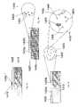
- FIG. 1shows a detection system according to an embodiment of the present invention
- FIG. 2shows a subsystem of a detection system according to an embodiment of the present invention
- FIG. 3shows a detection/identification subsystem of a detection system according to an embodiment of the present invention
- FIG. 4shows a waveguide circuit according to an embodiment of the present invention
- FIG. 5shows a waveguide circuit according to an embodiment of the present invention
- FIGS. 6 a and 6 bshow electronic processing according to an embodiment of the present invention
- FIG. 7shows an embodiment with dual reference arms according to the present invention
- FIGS. 8 a and 8 bshow a grating in a waveguide according to an embodiment of the present invention
- FIG. 9shows a corrugated waveguide with a porous polymer cladding according to an embodiment of the present invention.
- FIG. 10shows a grating in cladding according to an embodiment of the present invention
- FIG. 11shows channel waveguides according to an embodiment of the present invention
- FIG. 12shows a grating in a waveguide according to an embodiment of the present invention
- FIG. 13shows a waveguide according to an embodiment of the present invention
- FIGS. 14 a - 14 cshow a fabrication process for gratings according to an embodiment of the present invention
- FIG. 15shows a spectral diffraction efficiency according to an embodiment of the present invention
- FIG. 16shows a spectral diffraction efficiency according to an embodiment of the present invention
- FIG. 17shows a spectral diffraction efficiency according to an embodiment of the present invention.
- FIGS. 18 a - 18 cshow a process for obtaining an intensity distribution according to an embodiment of the present invention
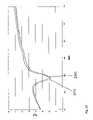
- FIG. 19shows transmission notches for different refractive indices according to an embodiment of the present invention.
- FIG. 20shows a spectral diffraction efficiency according to an embodiment of the present invention
- FIGS. 21 a and 21 bshow a spectral diffraction efficiency according to an embodiment of the present invention
- FIG. 22shows transmission scans according to an embodiment of the present invention
- FIG. 23shows a transmission scan according to an embodiment of the present invention
- FIG. 24shows a relation of absorbance to a concentration of antigen according to an embodiment of the present invention.
- FIG. 25shows a grating situated in a waveguide according to an embodiment of the present invention.
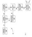
- a biological and chemical target agent sensor 10has a sample collection subsystem 20 that continuously draws samples of air, water, and soil from the environment.
- a transfer subsystem 30transfers the sample 40 from the collection subsystem 20 to working fluid 50 .
- a dispenser subsystem 60dispenses the working fluid 50 containing the sample into a detector module array (“DMA”) of a detection/identification (hereafter “ID”) subsystem 70 .
- DMAdetector module array
- IDdetection/identification
- the dual-function ID subsystem 70sends the sample data from the DMA through an electronic signal 80 to a data storage subsystem 90 .
- Data storage subsystem 90obtains and continuously compiles data from the DMA.
- the data within data storage subsystem 90may either be accessed directly or may be sent via an appropriate transmission system, such as telemetry subsystem 110 , for recording and analysis.
- the transmission systemmay send data at pre-selected intervals in batch format or, alternatively, may send data on a continual basis.
- the data storage system 90may perform analysis on the data from the ID subsystem 70 prior to forwarding for transmission.
- the data storage subsystem 90may be programmed to transmit data when a particular result is found, e.g., a target agent has been identified.
- the working fluid 50is transferred to a recirculation subsystem 120 .
- Recirculation subsystem 120decontaminates the working fluid 50 and returns the working fluid 50 to the transfer subsystem 30 to obtain another environmental sample.
- the recirculation subsystem 120consists of an ultrafine filter and an ultraviolet lamp that destroys/removes foreign material remaining in the working fluid.
- the working fluidis passed through micro-tubing and a low-flow pump. The working fluid then returns to the transfer subsystem 30 to pick up another sample 40 of the environment.
- the constant sampling and recirculationallows the system to continuously monitor the environment. In essence, it is “always on.”
- collection subsystem 20has an air sampler, preferably consisting of a pump for drawing through air from the environment, a horn or similar instrument for directing the air flow, a filter stage consisting of one or more filters to remove large particles, e.g., greater than 10 ⁇ m, and an exhaust system.
- the collection subsystem 20is adapted from conventional air samplers such as those provided by Airmetrics, Mattson-Garvin, SKC, or Sceptor Industries.
- the collection subsystem 20is adapted from conventional water samplers such as the Markland Duckbill® Sampling System, or an equivalent supplied by such companies as Global Water Instrumentation, Inc., and others.
- the water samplerconsists of a remote sampler head submerged in the water or a tube submerged in the water.
- a sampler pump/controllerdraws water samples through a filter stage to remove large particles, e.g., greater than 10 ⁇ m.
- the water sampleis then retained in a holding container for transfer of microscopic agents to the working fluid.
- the wateris then flushed out of the system to make room for the next sample.
- the collection subsystem 20is adapted from conventional soil water samplers such as those supplied by Soil Monitoring Engineering.
- Soil water samplerssuch as lysimeters or porous ceramic cups, are buried in the soil.
- a pumpcreates a partial vacuum, which causes water in the surrounding soil to enter the sampler via a porous ceramic filter.
- the sampleis then retained in a holding container for transfer of microscopic agents to the working fluid.
- the wateris then flushed out of the system to make room for the next sample.
- the environmental samplesare transferred to a working fluid by a transfer subsystem 30 .
- the transfer subsystem 30transfers potentially hazardous microscopic agents, as well as other microscopic constituents, from the environment to working fluid 50 of the sensor 10 .
- Transfer subsystem 30may be adapted from conventional products.
- the transfer subsystem 30is adapted from conventional gas bubblers, such as those supplied by SKC.
- the air sampleis bubbled through the working fluid, and gases from the atmosphere are dissolved in the fluid.
- the transfer subsystem 30is adapted from conventional particle impingers, such as those supplied by SKC. Aerosol particles impinge on the working fluid and become trapped in the liquid.
- the transfer subsystem 30is adapted from conventional dialysis cells, such as the DMLSTM supplied by Margan. The gradient of concentrations allows for material dissolved in the environmental water to diffuse into the working fluid 50 contained in the dialysis cell.
- the working fluid 50is typically an aqueous solution compatible with the molecular detectors.
- the working fluid 50continuously flows through the system to provide an always-on monitoring device.
- the working fluid 50necessarily comes into contact with the environment, it must be held at a constant temperature and appropriate chemical composition, e.g., pH, to optimize the sensor 10 and enhance the lifetime of the complex detector molecules, e.g., antibody proteins.
- a heater or a thermoelectric cooler systemcontrols the temperature of the working fluid for optimum operation of about 30-40° C.
- Dispenser subsystem 60receives the working fluid from transfer subsystem 30 .
- dispenser subsystem 60dispenses working fluid 50 , containing the microscopic environmental samples, to ID subsystem 70 comprising a multi-channel DMA.
- ID subsystem 70comprising a multi-channel DMA.
- a mixermechanically agitates the working fluid 50 to form a homogenous mixture of agents throughout the volume of the working fluid 50 . This ensures that when the working fluid passes from the dispenser 60 to the ID subsystem 70 , each channel of the DMA monitors identical samples.
- the working fluid 50After passing through a filter to separate out larger particles (e.g., greater than 1 ⁇ m or greater than 0.1 ⁇ m, depending on filter selection), the working fluid 50 then passes to an array of micro-wells.
- Each micro-well of the micro-well arrayis capable of holding approximately 1 ⁇ L of working fluid.
- one of an array of syringes 240draws a carefully metered volume of working fluid 230 , e.g., by use of a stepper motor 250 .
- a valve 270is then closed, and the syringe 240 dispenses the working fluid 230 via micro-tubing 220 to a micro-pipette 260 .
- the micro-tubing 220 delivering the working fluid 230 to the micro-pipette fluid dispensers 260may be similarly sized to catheter tubes.
- the micro-pipette fluid dispensers 260hold approximately 1 ⁇ L of fluid and are capable of accurately dispensing approximately 10-100 nL of working fluid.
- the micro-pipette fluid dispensers 260dispense the solution to the detector modules 280 of the DMA for identification of a target agent.
- the number of micro-wells 200 and fluid dispensers 260 in the array 210range in size from at least one to hundreds, depending on the number of agents that need to be monitored.
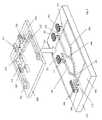
- a multi-channel DMA 300includes at least one to hundreds of individual detector modules or chips (hereafter “modules”) 305 , each designed to respond in a highly specific manner to one particular target agent. If one module 305 detects the presence of the particular target agent, then the specific module 305 reporting the decision automatically determines the identification of that target agent.
- a specific conjugate molecule or detector moleculee.g., antigen or antibody
- detector moleculebound to a grating, that in turn binds the target agent within the working fluid, determines agent specificity.
- agent specificityWith the exception of specific detector molecules per detector module, all other features of each module 305 are identical.
- the detector module 305identifies agents in the working fluid 50 .
- Micro-pipette dispensers 310 at a sample arm inlet reservoir 311 and control arm inlet reservoir 312 on the module 305introduce the working fluid 50 containing potentially hazardous agents, as well as other inert material, to the module 305 .
- Each reservoir 311 , 312typically holds 100-1000 nL of solution.
- Micro-fluidic channels 315having exemplary cross sectional areas of approximately 10 ⁇ 10 ⁇ m 2 to 100 ⁇ 100 ⁇ m 2 , direct the solution, i.e., working fluid and inert materials, in the sample and control arms to porous polymer Bragg gratings 320 , 321 .
- Pressure gradientsmay induce fluid flow within the micro-fluidic channels 315 .
- additional electrodes in the modulemove the solution along the channel by electrophoresis and/or electroosmosis.
- the porous Bragg gratings 320 , 321allow the solution to flow through.
- An outlet micro-pipette 325collects the material at the outlet reservoir 326 .
- Proper filtering in the collection subsystem 20 and dispenser subsystem 60 of FIG. 1ensures that particles are small enough to pass through the pores of the gratings 320 , 321 .
- sample grating 320acts chemically as a “selectively sticky” filter through detector molecules that are bound in the pores and/or on the surface of the sample grating 320 .
- Inert materialsflow through the filters of subsystems 20 and 60 and the sample grating 320 , but target agents are selectively bound to a corresponding detector molecule and become a permanent part of the grating.
- the porous polymer Bragg gratings 320 , 321 , 322act as narrow band spectral filters with a reflection or transmission notch that is highly sensitive to refractive index changes.
- the selective bindingmodifies the refractive index of the grating.
- the control grating 321has no detector molecules and hence does not selectively trap any target agents.
- the ID subsystem 70is sensitive to the refractive index changes in the gratings 320 , 321 . If the refractive index changes, a transduction mechanism then provides a signal to alert the system 70 of the presence of an agent.
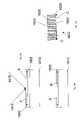
- each module 305consists of an optical channel waveguide 335 comprised of three arms: (1) a sample arm 330 , (2) a control arm 331 , and (3) a reference arm 332 . All three arms contain identically fabricated porous polymer Bragg gratings 320 , 321 , 322 .
- the porous polymer Bragg gratings 320 , 321 , 322have been integrated onto the module along with a light source 340 , waveguides 335 , waveguide splitters 345 , 346 , micro-fluidic channels 315 , photodetectors (i.e., photodiodes) 350 , 351 , 352 and processing electronics 360 .
- the response from each arm 330 , 331 , 332is continuously and simultaneously monitored and processed electronically to factor out environmental disturbances, including inert material in the sample, to achieve a high sensitivity and a low false alarm rate.
- Lightis launched into the waveguide from the light source 340 , which may be a broadband light emitting diode (“LED”) or preferably a single-frequency laser diode (“LD”).
- the light source 340which may be a broadband light emitting diode (“LED”) or preferably a single-frequency laser diode (“LD”).
- LEDbroadband light emitting diode
- LDsingle-frequency laser diode
- a portion of the lightis directed to the reference arm 332 containing a reference grating, and subsequently, a photodetector 352 .
- the reference gratingis hermetically sealed; it never is exposed to the working fluid 50 .
- the reference gratingmay or may not contain a pure solution in its pores.
- the optical properties (e.g., index of refraction) of the reference gratingchange only due to thermal changes in the system.
- Energy detected at the photodetectors 350 , 351will also change due to thermal drift of the reflection notch or light source fluctuations.
- the fluctuationsare removed by taking the difference of the sample grating 320 and control grating 321 signals.
- the processing electronics 360can subtract the reference grating arm 332 signal from both the sample grating 330 and control grating 331 arm signals. Since all three gratings 320 , 321 , 322 and their respective photodetectors 350 , 351 , 352 are located on the same module 305 , the gratings 320 , 321 , 322 experience the same fluctuations due to thermal drift, light source fluctuations, and other disturbances. This process thus removes spurious signals due to the detector environment.
- the reference grating arm 332can also maintain the wavelength of the light source tuned to the Bragg grating 322 . As the Bragg grating notch drifts due to thermal drift, the signal from the reference grating arm 332 passes through a feedback loop to the light source 340 to tune the wavelength of the source to the notch wavelength of the Bragg grating 322 . The remaining signals are the result of foreign material, i.e., agents, present in the working fluid. Inert material passes through the gratings and produces transient changes in the refractive index. As a result, transient signal responses are produced at the photodetectors 350 , 351 .
- the signals from the sample grating 330 and control grating 331 armsare integrated over an appropriate time interval (e.g., by sample and hold circuits) and then subtracted (e.g., by a differential amplifier). Since both arms, 330 and 331 , identify, on the average, the same amount of inert material, these signals will cancel, producing a null signal. However, if target agents, i.e., molecules, are present, the target agents stick to the sample grating 320 and permanently change its refractive index. Moreover, the refractive index change increases with each captured target agent. Since the reflection notch is spectrally narrow, a relatively small change in refractive index produces a large change in filter transmittance.
- the subsequent change in the transmitted light over the integration intervalupsets the balance in the two arms 330 and 331 .
- the difference signalis passed through a differential amplifier in the electronic processor 360 .
- the presence of a non-zero signalheralds the presence of the target agent. Once a target agent detection is accomplished, that specific detector module 305 is replaced before the system is used in another monitoring scenario.
- FIGS. 4 and 5provide additional description of component parts according to an embodiment of the present invention.
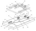
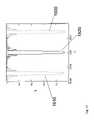
- detection module 405includes a light source 440 , a channel waveguide 435 , gratings 420 , 421 , 422 , a micro-fluidic circuit 415 , photodetectors 450 , 451 , 452 , and processing electronics.
- the processing electronicsare not shown in FIGS. 4 and 5 .
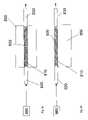
- the module 405resides on a silicon wafer 470 .
- Light source 440 , photodetectors 450 , 451 , 452 , and large scale integration processing circuitryare either mounted directly on the silicon wafer 470 or integrated monolithically with the silicon wafer 470 , at electrodes 475 , 476 , 477 , 478 .
- the silicon wafer 470is coated with a silicon dioxide (SiO 2 ) layer 480 .
- Micro-fluidic circuit 415as well as the fluid input 411 , 412 and output 426 ports, are etched in the SiO 2 layer 480 .
- the SiO 2 /SiON channel waveguide 435 and micro-fluidic circuit 415are covered with a glass slab 490 .
- the Bragg gratings 420 , 421 , 422are situated in the channel waveguide 435 .
- a rectangular cavityis etched in the channel waveguide 435 at the position selected for each of the gratings. This cavity is then filled with a pre-polymer syrup described herein, and a porous polymer grating is formed by the procedures discussed further with respect to at least FIGS. 14 a - 14 c .
- Micro-fluidic circuit 415is etched in the SiO 2 layer 480 as shown, and the micro-fluidic channels are directed in a substantially perpendicular direction to the long dimension side of the gratings 420 , 421 .
- the working fluid of the devicewill flow through the porous gratings 420 , 421 at an angle substantially perpendicular to the channel waveguide 435 axis.
- the surface of layer 480is exposed to air.
- the SiO 2 /SiON waveguide circuit 435 and micro-fluidic circuit 415are covered with a glass sheet 490 to seal the micro-fluidic circuit 415 and the porous polymer Bragg gratings 420 , 421 , 422 from the environment, e.g., air.
- Small pilot holes 491 , 492 , 493are etched in the glass 490 to match up with the inlet/outlet ports 411 , 412 , 426 of the micro-fluidic circuit 415 on the module 405 .
- An electrical feed-through 495is also provided for reference photodetector 452 .
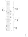
- detection module 505resides on a silicon wafer 570 .
- a SiO 2 layer 580is coated with a polymer layer 590 , such that the polymer has an index of refraction smaller than the SiON channel waveguide 535 .
- Porous polymer Bragg gratings 520 , 521 , 522are situated in the polymer cladding layer 590 .
- Micro-fluidic circuit 515is etched in the polymer cladding layer 590 .
- the fluid input 511 , 512 and output 526 portsare likewise etched in the polymer layers 590 .
- the polymer cladding 590includes an electrical feed-through 595 for the reference photodetector 552 .
- a laser diode 540 and photodetectors 550 , 551contact electrodes 575 , 576 , 577 .
- the Bragg gratings 520 , 521 , 522are situated in the cladding directly above the channel waveguide 535 .
- the SiO 2 layer 580 containing the SiON channel waveguide 535is coated with a polymer cladding 590 .
- a rectangular cavityis etched in the polymer cladding 590 at the positions selected for the gratings. This cavity is then filled with a pre-polymer syrup described herein, and a porous polymer grating is formed by the procedures discussed further with respect to at least FIGS. 14 a - 14 c .
- Micro-fluidic circuit 515 and inlet/outlet ports 511 , 512 , 526are etched in the polymer cladding 590 as shown, and the micro-fluidic channels are directed in a substantially perpendicular direction to the long dimension side of the gratings 520 , 521 . In this manner, the working fluid of the device will flow through the porous gratings 520 , 521 at an angle substantially perpendicular to the channel waveguide 545 axis.
- the polymer cladding 590is exposed.
- the polymer cladding 590is covered with a glass sheet to seal the micro-fluidic channels 515 and the porous polymer Bragg gratings 520 , 521 , 522 from the outside environment. Small pilot holes are etched in the glass to match up with the inlet/outlet ports 511 , 512 , 526 of the micro-fluidic circuit in the polymer cladding 590 .
- the light sources 440 and 540are preferably a laser diode (“LD”).
- LDlaser diode
- tertiary semiconductor laserssuch as Al x Ga 1 ⁇ x As
- quaternary semiconductor laserssuch as In 1 ⁇ x Ga x As 1 ⁇ y P y
- the ratios x and ycan be varied to adjust the laser wavelength.
- AlGaAs lasersgenerally provide wavelengths between 750 nm and 870 nm.
- In 1 ⁇ x Ga x As 1 ⁇ y P y lasersgenerally provide wavelengths between 1.1 ⁇ m and 1.6 ⁇ m.
- Visible wavelength laserssuch as GaInP (670 nm) and AlInP (584 nm), may also be useful.
- the LDis bonded upside-down to an electrode on the silicon surface and butt-coupled to the SiON channel waveguide.
- waveguides 435 , 445 , 446 , 447 , 535 , 545 , 546 , and 547may be formed of SiON as a core material.
- the refractive index of SiONcan be varied between 1.46 and 2.3.
- the SiON refractive indexcan be tuned to be greater than that of SiO 2 to form a waveguide.
- the refractive indexcan be matched to that of the polymer (approximately 1.52) used in the inline Bragg gratings, or tuned to be slightly larger than the polymer that is used as the cladding layer.
- the optical outputs of the reference 447 , 547 , sample 445 , 545 , and control 446 , 546 waveguide channelsare coupled to photodetectors 450 , 451 , 452 , 550 , 551 , 552 .
- the photodetectors 450 , 451 , 452 , 550 , 551 , 552are mounted upside-down and bonded to electrode pads 475 , 476 , 477 , 575 , 576 , 577 on the silicon wafer 470 , 570 .
- silicon photodiodesmay be used.
- AlGaAsP photodiodesmay be used for wavelengths in the range of about 900 nm to 1600 nm.
- FIGS. 6 a and 6 ban embodiment illustrates the type of electronic processing applied to the photodetector outputs for the sample and control channels of FIGS. 3 , 4 , and 5 .
- FIG. 6 aonly inert material flows through both the sample and control porous polymer Bragg gratings.
- target agents, along with the inert materialpass through the gratings. In each of FIGS.
- the electronic processing systemconsists of four main parts: (1) sample and hold circuits 600 , 601 ; (2) differential amplifier 610 ; (3) analog-to-digital (A/D) converter 605 ; and (4) additional digital processing electronics 615 .
- the sample and hold circuits 600 , 601sample voltages from the photodetectors over a specified time interval.
- the time intervalis selected by a negative pulse of a predetermined time interval applied to the gate of a p-channel MOSFET 670 , which closes a switch and allows data in the form of a stream of voltage pulses from photodiodes to pass through the switch and be stored on a capacitor 620 , 625 .
- These pulsesas illustrated in the embodiment in FIG. 6 a , represent transient responses from the photodiodes due to inert material flowing through the gratings and producing fluctuations in the average refractive index. This leads to the transmission of transient light pulses through the grating that are detected by the photodiodes.
- the sample and hold circuitsreceive input from a control data stream 630 , 631 and corresponding gate pulse 635 , 636 , as well as sample data stream 640 , 641 and corresponding gate pulse 645 , 646 .
- the inputis received through amplifiers 675 .
- the output of the sample and hold circuits 600 , 601 , at the end of the gate pulse,are dc voltages, V C 650 , 651 , for the control channel, and V S 655 , 656 , for the sample channel.
- V C and V Srepresent the sum of voltage spikes from their respective channel. These voltages are input to a differential dc amplifier 610 that employs one operational amplifier 660 .
- the conventional offset-voltage balancing circuitry standard for differential amplifiersis not shown.
- Output V out 665 , 666is equal to (R 2 /R 1 )(V S ⁇ V C ). Therefore, output V out 665 of the differential amplifier 610 should be approximately zero.
- Output V out 666does not equal zero.
- a standard A/D circuit 605digitizes the output voltage. This data is stored and/or processed further. For example, averages are computed over several sampling intervals to improve the sample statistics. Other more complex data processing can also be accomplished.
- target agentsstick to the sample Bragg grating in sample data stream 641 resulting in a non-zero persistent voltage baseline on which transients, due to inert material, ride as voltage fluctuations. The output of the differential amplifier is non-zero, thus signaling a target-molecule detection event.
- the above schemealso discriminates real signals from photodiode voltage fluctuations and drift that may occur due to light source power fluctuations, thermal drift, and other environmental disturbances. Since the two detector arms reside on the same module, they are subject to the same external disturbances. Voltages produced due to these effects are common to both channels and subtracted out by the differential amplifier.
- Voltage drift due to external influencesmay also be factored out by using the output of the reference arm of the module in a set of circuits similar to those of FIGS. 6 a and 6 b , comparing the reference output with the sample and control outputs separately.
- Thermal driftmay cause the Bragg grating notch to wander off the laser wavelength due to thermal changes in the refractive index.
- the reference arm photodiodemay be used in a feedback loop to tune the laser wavelength to match any thermal drift of the Bragg gratings and lock the laser wavelength to the Bragg condition.
- Diode lasersare available whose output wavelengths can be tuned electronically over a few nanometers.
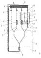
- the reference armcould be replaced with a dual reference arm using an additional Y-splitter.
- a sealed porous polymer Bragg grating 710on an SiO 2 layer 705 substantially coating a Si substrate 700 , terminating at a photodiode 720 , and the second reference arm 716 would have no grating and terminate at a separate photodiode 721 .
- the outputs of the two reference arms 715 , 716are compared to discern thermal drift of the Bragg grating 710 from fluctuations or drift of the output power from the laser diode 725 .
- Sample and control arms 730 , 740are directed to gratings 735 , 745 proximate micro-fluidic channels 750 . All photodiodes 720 , 721 , 722 , 723 lead to an electronic processor 760 with an LD stabilization feedback loop 770 to the laser diode 725 .
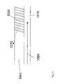
- a porous polymer Bragg grating 2500is situated in a channel waveguide 2510 .
- Lightis confined to the waveguide 2510 by total internal reflection at the substrate 2550 and cladding 2540 .
- Light at the Bragg wavelength propagating along the waveguide 2510is reflected from the grating 2500 and propagates back along the waveguide 2510 in the opposite direction. Therefore, transmitted light at the Bragg wavelength is attenuated.
- a porous polymer mediumserves as cladding 940 for a corrugated waveguide 910 .
- the pre-polymer syrupis cured using a single incoherent beam of light such that no grating is recorded.
- the phase-separated liquid crystalis then removed to yield the porous polymer cladding.
- the corrugated waveguide 910acts like a Bragg grating. Incident light is shown as 960 and reflected light is shown as 970 within FIG. 9 .
- Light evanescently coupled to the porous cladding 940will sense any change in the refractive index of the cladding 940 . This would produce a spectral shift of the reflection notch of the filter. Changes in the refractive index of the grating change the efficiency of the evanescently coupled light.
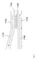
- an alternative embodimentplaces a porous polymer Bragg grating 1000 in the cladding 1040 .
- Guided light 1060 through waveguide 1010experiences spectrally selective loss to radiation modes 1070 by evanescently coupling to the Bragg grating 1000 in the cladding 1040 .
- two channel waveguides 1110 , 1115are coupled evanescently to form a waveguide coupler, directing out-coupled light 1170 and input light 1160 .
- a holographic grating 1100 in the cladding region 1140serves to spectrally assist this coupling for light at the Bragg wavelength.
- Out-coupled light 1170is directed into the opposite direction in the output waveguide 1110 .
- This configurationprevents reflected light from impinging back on the light source.
- a long periodi.e., where ⁇ is substantially greater than ⁇
- porous polymer grating 1200is placed in a waveguide 1210 substantially on a substrate 1250 .
- Such a grating 1200serves to resonantly couple light 1260 at a specific wavelength to radiation modes 1270 .
- an asymmetric waveguide 1310has a Bragg reflection grating 1300 serving as the substrate.
- Light 1360 resonantly coupled to the Bragg condition of the grating 1300follows a zigzag path down the slab waveguide 1310 .
- a single Bragg grating in a waveguide channelcan be used as a stand-alone detector element.
- a porous polymer Bragg grating 800is situated in a channel waveguide 810 , as a stand-alone element, optically coupled to input optical fibers 820 and output optical fibers 830 .
- Waveguide 810 and grating 800are proximate to substrate 850 .
- An LED or LD source 860launches a wave into the fiber 820 , which is coupled into the Bragg grating 800 and subsequently out-coupled to a miniature spectrometer (not shown), such as the S2000 manufactured by Ocean Optics Inc. The spectrometer monitors any real-time changes to the diffraction efficiency of the grating 800 .
- certain embodiments of the present inventionutilize polymer-dispersed liquid crystal (“PDLC”) or holographic PDLC (“HPDLC”) related technology in the formation of the Bragg gratings and waveguide components.
- PDLCpolymer-dispersed liquid crystal
- HPDLCholographic PDLC
- Descriptions of PDLC materials and related technologycan be found in U.S. Pat. No. 5,942,157, U.S. patent application Ser. No. 09/363,169 filed on Jul. 29, 1999 for Electrically Switchable Polymer Dispersed Liquid Crystal Materials Including Switchable Optical Couplers and Reconfigurable Optical Interconnects, U.S. patent application Ser. No. 10/235,622 filed on Sep.
- the Bragg gratingscomprise static holograms formed through holographic polymerization of a PDLC material using coherent light beams.
- the liquid crystalis removed from the film. Extraction of the liquid crystal leaves pores within the remaining polymer matrix approximately 100 nm in diameter.
- the pores within the polymer matrixcontain binding sites, such as COOH or NH 2 , for a detector molecule.
- the polymermay be thiol-ene, thiol-acrylate, or one of various multifunction acrylates described in U.S. Pat. No. 5,942,157.
- the polymercan be cured via visible or ultraviolet (“UV”) laser radiation.
- UVvisible or ultraviolet
- the evacuated polymer matrixis then chemically treated to activate the binding site for the detection molecule.
- the activation proceduredepends on the functional group of the binding site.
- amine couplinge.g., EDC (N-ethyl-N′-(3-dimethyl aminopropyl)-carbodiimide hydrochloride) and NHS (N-hydroxysuccinimide
- EDC/NHS coupling procedureis an accepted procedure commonly referred to as EDC/NHS coupling procedure.
- an accepted procedureis cross-linking to free amino groups via polymerized gluteraldehyde.
- any method that activates the binding site to bind to a detector moleculeis sufficient.
- a detector moleculeis bound to the activated binding site.
- This detector moleculethen can sense a target agent of interest.
- the detector moleculecan be an enzyme, a protein, an antibody, or an antigen.
- the detector moleculeis specifically selected to bind to the target agent.
- the binding sites that are unattached to any detector moleculeare blocked using conventional means. The blocking is usually achieved with a large protein, such as casein or BSA.
- the target agentbinds to the detector molecule, it causes a change in the refractive index of the polymer, thus causing a shift in the wavelength of the holographic notch.
- a pre-polymer syrupconsisting of a mixture 1405 of polymerizable monomer, photoinitiator, co-initiator, liquid crystal, binding site monomer, and in alternative embodiments, a cross-linking monomer and a long chain aliphatic acid are spread in a thin layer, typically about 10 ⁇ m, in slab waveguide format on a substrate 1410 .
- two coherent beams of light 1415are incident on the mixture 1405 , forming a pattern consisting of PDLC 1420 a and polymer 1420 b channels within the mixture 1405 , as shown in FIGS. 14 b and 14 c .
- the polymerized material 1420is referred to as HPDLC material, since the overlapping coherent beams 1415 form an interference pattern within the photopolymerized material 1420 .
- portions of monomer from mixture 1405are consumed forcing the remaining monomer to diffuse and replace the consumed portions of monomer, forming polymer channels 1420 b .
- the liquid crystal phasetakes the form of interconnected nanoscale droplets of liquid crystal 1425 within a polymer matrix 1430 .
- the nanoscale domains of liquid crystal 1425are of controllable density and size.
- the liquid crystal 1425is then extracted by: (1) soaking the hologram with a solvent followed by drying; (2) vacuum evacuating the pores; or (3) a combination of (1) and (2).
- poresinterconnected voids or pores 1435
- the resulting hologram with pores 1435is then treated chemically to activate the binding sites 1450 then attach detector molecules 1440 (i.e., antibodies) to the activated binding sites 1450 .
- detector molecules 1440i.e., antibodies
- antigens 1445may attach to detector molecules 1440 .
- the Bragg grating formed by this processmay then be used in the detector modules described with reference to, for example, FIGS. 5-7 , in order to detect target agents within the working fluid.
- the polymer matrix 1430has a refractive index of about 1.52, while that of the aqueous solution is approximately 1.33.
- the periodic index mismatchcreates an index modulation or an optical grating.
- the gratingexhibits Bragg diffraction for light at a specific wavelength propagating at a specific angle of incidence.
- the hologramis a Bragg reflection grating that retro-reflects light at the Bragg wavelength.
- the Bragg wavelengthis determined by the average refractive index and the periodic spacing of the porous regions.
- the strength of the reflectioni.e., the diffraction efficiency, is determined by the magnitude of the index modulation and the physical length of the filter, i.e., region of index modulation.
- the diffraction efficiencywill become larger with increased filter thickness, and the spectral width of the reflection notch will decrease with increased filter thickness.
- the index modulationis determined by the difference in refractive indices of polymer matrix and aqueous solution, which in this exemplary embodiment is approximately 0.19, and the density of pores.
- a low index modulationcan thus be achieved by a low density of pores.
- a small density of pores, i.e., low index modulation, and a thick filteris achieved in a waveguide configuration, resulting in a spectrally narrow filter with large diffraction efficiency. Nonetheless, the specific pore density must be consistent with a sufficient flow rate of working fluid through the hologram. Specific grating compositions are described further below.
- the selected Bragg wavelengthis determined by such factors as the chosen laser wavelength and the spectral region of sensitivity desired for detecting a refractive index shift based on the polymer and detector molecule reaction selected. This optical region may be anywhere across the visible or near infrared spectrum.
- the Bragg wavelength ⁇ B for light propagating substantially along the waveguide axisis approximately 2n ⁇ , where n is the average refractive index of the medium at ⁇ B .
- the index nchanges as target agents are bound to the polymer matrix.
- the bandwidth ⁇ of the spectral diffraction efficiency for a Bragg gratingis given by:
- ⁇ ⁇ ⁇ ⁇⁇ B 2 ⁇ ⁇ ⁇ n ⁇ ⁇ 2 + ( ⁇ / L ) 2
- ⁇the coupling constant of the grating
- Lthe grating thickness.
- the bandwidthis inversely proportional to the thickness.
- a thicker gratingleads to a sharper reflection notch.
- the thicker gratingalso increases the diffraction efficiency.
- the bandwidthis directly proportional to ⁇ .
- a small coupling constant ⁇i.e., a small index modulation
- a thick filter with a small index modulationyields a grating with high peak diffraction efficiency and a narrow spectral notch.
- the index modulation of the gratingis produced by the periodic variation of nanoscopic pores throughout the volume of the polymer.
- the density of poreshas the form of a rectangular wave, with a volume fraction of pores f c in a channel of width ⁇ , (0 ⁇ 1) and no pores in adjacent channels of width (1 ⁇ ) ⁇ .
- the index modulationis related to the first Fourier component of the Fourier expansion of this rectangular wave, and is given by:
- n 12 ⁇ ⁇ f c ⁇ ⁇ sin ⁇ ( ⁇ ⁇ ⁇ ⁇ ) ⁇ ( n p - n s )
- n p and n sare the refractive indices of the polymer and solution filling the pores, respectively.
- the parameters f c and ⁇are determined by the phase separation of liquid crystal during the recording of the holographic grating. These are controlled by processing parameters such as recording intensity and total exposure, as well as material properties including liquid crystal concentration and concentrations of other recipe constituents, such as long chain aliphatic acids. With the refractive indices relatively fixed at n p approximately equal to 1.52 and n s approximately equal to 1.33, the index modulation is directly controlled by the values of f c and ⁇ .
- the index modulation n 1is 0.039.
- a filter response with the same peak efficiencyhas a reduced bandwidth.
- the corresponding index modulation n 1is 0.0098.
- a filter at least this thickis readily achieved in a waveguide configuration.
- a sharper reflection notchgives a more sensitive change in transmittance with changes in refractive index.
- a holographic recording method for creating a porous polymer gratingenables users to set processing parameters in order to easily obtain the index modulation for the sharp reflection notch.
- the index modulation amplitudefalls off as a Gaussian function toward the front and back of the grating.
- Such a gratingis obtained holographically by giving the recording beams a Gaussian intensity distribution.
- Gaussian intensity distributionis achieved by passing the beams 1815 through at least one neutral density filter 1800 , over a pre-polymer syrup mixture 1805 on a substrate 1810 , with optical density that has an inverse Gaussian distribution.
- Other filters or maskscan produce other types of apodizing functions, such as raised cosine, hyperbolic tangent, polynomial, or other apodizations based on mathematical distributions.
- the transparency of the at least one neutral density filter 1800substantially decreases in the direction of arrows A. Referring to FIGS.
- resulting grating 1822has a pore distribution that follows the local intensity of the recording beams 1815 .
- the transparency of the PDLC hologram 1820substantially increases in the direction of arrows B as shown in FIG. 18 b .
- the resulting grating 1822has alternate polymer slabs 1830 and porous slabs 1835 .
- the pore density of the porous slabs 1835substantially decreases in the direction of arrows C.
- Sensitivityis built into the detection in two ways.
- the filter reflection or transmission notchis very sharp spectrally and exhibits a large change in transmittance for a relatively small change in refractive index.
- the binding sites of the pores or polymer matrix of the hologramsare chemically activated and the detector molecules are bound to the polymer matrix.
- a target agentis present in the working solution, it will selectively bind to the detector molecules.
- the target agentbecomes trapped in the pore. Since the chemical nature of the polymer matrix changes, the average refractive index also changes. Consequently, the spectral properties of the porous polymer Bragg grating also change.
- Bound target agentsmodify the spectral properties of the sample grating by changing the refractive index and possibly swelling the polymer.
- the diffraction efficiency of the sample gratingis very sensitive to these changes.
- the spectral shift ⁇ B of the gratingis determined by
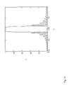
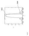
- a spectral shift of 1 nmproduces a very significant change in the transmittance of the filter. Referring to FIG.
- transmission notches 1910are shown for three different refractive indices for a filter irradiated by a broadband light source, e.g., LED.
- Transmission notch 1910shifts with a decrease of index
- transmission notch 1930shifts with an increase in index.
- the effectsare similar to the swelling of polymer, i.e., a change of grating period.
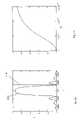
- the sensitivity of the sample gratingmay be enhanced by interrogating the grating at a wavelength near a region of rapidly changing efficiency.
- the diffraction efficiency ⁇i.e., reflection; transmission equals 1 ⁇
- ⁇tan h 2 ( ⁇ L ) where ⁇ is the coupling coefficient and L is the filter thickness.
- the relative change ⁇ / ⁇ in diffraction efficiencyis given by:
- ⁇ ⁇ ⁇ ⁇ ⁇16.8 ⁇ ⁇ n 2 ⁇ ⁇ ⁇ ⁇ L ⁇ L ⁇ B 2 ⁇ ⁇ ⁇ ⁇ ⁇ for changes in refractive index and grating period, respectively.
- the laser wavelength ⁇ L 2010is approximately 850.075 nm.
- optical differential gaina relatively small change in index or period produces a relatively large change in transmittance.
- the laser wavelength 2110is at a null in the diffraction efficiency.
- a small change in refractive indexthen produces a rapid rise in the diffraction efficiency 2120 from a zero background.
- the benefit of this effectis realized when the photodetector is placed to view reflected light rather than transmitted light.
- gratingsare constructed using thiol-acrylate as the polymerizable monomer and 2-carboxyethylacrylate (2-CEA) as the binding site monomer, with 10- ⁇ m thickness achieved by sandwiching the mixture between two glass plates.
- These gratingshave one glass substrate coated with a release agent. The release agent substrate is removed, and the gratings are evacuated in a vacuum oven over a period of approximately three days to remove the liquid crystal.
- the cellsare scanned in, for example, a Cary 500 UV/VIS spectrophotometer from Varian.
- the sensor molecule Gliadinis bound to the grating to sense the anti-Gliadin target agent.
- the carboxy groupBefore attachment of Gliadin to the carboxy (COOH) group of the HPDLC, the carboxy group is activated using the EDC/NHS coupling procedure. After activation of the groups, the Gliadin is attached. Following attachment, another protein, casein, is used to block carboxy groups that were not attached to Gliadin. Casein does not interfere with the target agent attachment, since the anti-Gliadin antibodies are specific for Gliadin.
- a batch of HPDLC gratingsare made on BK7 optical flats at 25- ⁇ m thickness.
- the gratingsare evacuated over approximately three days to remove the liquid crystal.
- Certain gratings from the batchare checked with an ELISA (Enzyme Linked Immuno Specific Assay) kit, and other gratings are scanned in a spectrometer for a peak shift.
- the ELISA checked gratings and the spectrometer scanned gratingsare tested with either standard A or standard F.
- the pre-selected spectral absorbanceis proportional to concentration, i.e., A is the lowest concentration and F is the highest.
- the HPDLC gratingswithstand treatment with all the solutions needed for protein and antibody attachment without degrading.
- Exemplary embodimentsinvolve a grating sensing anti-Gliadin, or an alternative embodiment sensing Cortisol.
- Materials used in the exemplary embodimentsinclude the monomer dipentaerythritol hydroxy penta acrylate (DPHPA), photoinitiator dye Rose Bengal (RBAX), co-initiator N-phenylglycine (NVG), monomer N-vinylpyrrollidone (NVP), long-chain aliphatic acid dodecanoic acid (DDA), binding site monomer 2-carboxyethylacrylate (2-CEA), and liquid crystals E7 and TL213 (both available from Merck).
- DPHPAmonomer dipentaerythritol hydroxy penta acrylate
- RBAXphotoinitiator dye Rose Bengal
- NVGco-initiator N-phenylglycine
- NVPmonomer N-vinylpyrrollidone
- DDAbinding site monomer 2-carboxyeth
- Gliadinan antigen derived from wheat, is utilized as the sensor molecule to detect the presence of anti-Gliadin.
- the recipeincludes 47.9% DPHPA, 0.6% RBAX, 1.5% NPG, 10.0% NVP, 38.0% E7, and 2.0% 2-CEA.
- the above formula, less the 2-CEA,is a conventional formulation for recording HPDLC gratings, and is given the designation CS573. A holographic recording in such a mixture results in a periodic distribution of interconnected liquid crystal droplets.
- the addition of 2-CEAprovides COOH groups attached to the polymer matrix, with some COOH groups residing at the polymer/liquid crystal droplet interfaces.
- the pre-polymer mixturealso includes 15 ⁇ m glass rods that act as spacers for the holographic cell which comprises two 1′′-diameter, 1 ⁇ 8′′-thick glass windows.
- a sonicatorhomogenizes the mixture prior to sandwiching the pre-polymer mixture within the holographic cell, between the glass windows. At least one of the glass windows is coated with a release agent to facilitate removal of one substrate after holographic recording.
- a 1-hour white-light post-cure procedurebleaches the remaining RBAX dye.
- the release-agent-coated flatis separated from the photopolymerized material, and the transmittance spectrum of each photopolymerized material is measured using, for example, a Cary500 UV/VIS/NIR spectrometer.
- the nominal peak of the reflection notch(minimum of the transmittance curve) is around 535 nm.
- the hologramsare placed in a vacuum oven (approximately 28 mm Hg) for a period of about 48 hours to extract the liquid crystal. After removing the holograms from the oven, the samples are rinsed in methanol and replaced in the oven for 3 hours. Each cell is then measured again in the Cary500. All samples exhibit a blue shift of the diffraction peak, indicating that the liquid crystal is removed, and the refractive index of the composite medium is decreased.
- Phase Isolution samples containing different concentrations of target molecules are pipetted onto the Bragg gratings. Any present target agents bind to the inner surface of the Bragg grating. After a 30-minute incubation the grating is washed with wash buffer for removing non-reactive components. Phase I includes incubation with Gliadin (I w/G) or no incubation with Gliadin (I w/o G).
- sample Bragg gratings in subsets A and Bare air-dried overnight. All sample Bragg gratings exhibit a red shift of the diffraction notch, with the non-Gliadin samples having about twice the shift of that of the Gliadin samples, due to the increased refraction index.
- materiale.g., Gliadin and/or casein
- Gliadinis added to the vacant pores of the sample, attaching to the activated COOH sites, and thereby increasing the refractive index.
- the molecular weight of Gliadinis approximately 50,000 Daltons.
- Caseina protein found in milk, exists most often as a micelle, with an average molecular weight of approximately 375,000 Daltons.
- sample Bragg gratings containing only caseinhave more mass and thus a higher refractive index than those sample Bragg gratings containing a mixture of casein and Gliadin.
- a higher refractive indeximplies a larger shift of the diffraction notch.
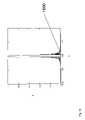
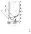
- sample Bragg gratings 3 and 2are air-dried overnight. Both sample Bragg gratings exhibit an additional shift, indicating the binding of the anti-Gliadin to the Gliadin. All four spectrometer transmission scans in the above sequence for sample Bragg grating 3 , as exemplified in FIG.
- FIG. 22illustrate an initial scan 2200 after recording with liquid crystal droplets in the Bragg grating, a blue shifted scan 2210 after the pores are evacuated (liquid crystal removed), a subsequent red shift 2220 when Gliadin and casein are bound to the activated COOH sites, and a final red shift 2230 when the antibody binds to the Gliadin, thereby increasing the refractive index, i.e., adding mass to the pores.
- the final red shift 2230is about 1%.
- Sample Bragg grating 2exhibits a final red shift of approximately 6%, a larger shift due to a higher concentration of antibodies.
- Sample Bragg gratings 5 , 6 , 8 , 9 and control 1are subjected to Phases II and III of the procedure.
- Phase IIthe sample Bragg gratings are incubated in an anti-human-IgA horseradish peroxidase conjugate solution, which recognizes IgA class antibodies bound to the immobilized antigens.
- a wash bufferthen washes away any excess enzyme conjugate not specifically bound to the antibodies.
- a chromogenic substrate solution containing TMB (3,3′,5,5′-Tetramethylbenzidine)is dispensed onto the gratings.
- TMB3,3′,5,5′-Tetramethylbenzidine
- the color of the solutionschanges from a clear solution to blue.
- the addition of 1 M hydrochloric acidstops color development to stabilize the sample for spectrometer measurements.
- the solutionchanges color to yellow.
- the amount of coloris proportional to the concentration of IgA antibodies present in the original sample. A higher concentration of IgA produces a larger absorbance at 450 nm.
- the color changes of sample Bragg gratings 5 , 6 , 8 , 9 and control 1are quantified by measuring the absorbance of the samples at 450 nm.
- sample Bragg gratings 5 and 8both treated with Gliadin, exhibit larger absorbance than cells not treated with Gliadin ( 6 and 9 ), with the larger difference being between sample Bragg gratings 8 and 9 that are exposed to the higher concentration of IgA.
- the control sample Bragg grating 1exhibits an absorbance similar to sample Bragg grating 6 , which follows since neither sample Bragg grating was treated with Gliadin.
- a solution of TMB and HClis formed without any exposure to the sample Bragg gratings. This solution exhibits no absorbance at 450 nm.
- cortisolis the antigen and the sample Bragg grating is activated with anti-cortisol to form a detector sensitive to the presence of cortisol.
- Cortisolis a hormone present in the body and released in higher quantities during stressed or agitated states.
- the mixturealso includes 8- ⁇ m glass rods as spacers for the holographic cell, and a sonicator homogenizes the mixture.
- the resulting syrupis then sandwiched between two 1′′-diameter, 1 ⁇ 8′′-thick glass windows.
- At least one of the glass windowsis coated with a release agent to facilitate removing one of the substrates.
- Reflection hologramsare prepared using 532-nm beams. A 1-hour white-light post-cure bleaches remaining RBAX dye.
- One substrateis removed from each of the sample Bragg gratings and the gratings are scanned in the Cary500. The nominal notch wavelength is 536 nm.
- sample Bragg gratingsare then split into four groups for further treatment: (A) anti-cortisol attachment with subsequent incubation in cortisol; (B) anti-cortisol attachment with no subsequent incubation in cortisol; (C) no antibody attachment with subsequent incubation in cortisol; and (D) anti-cortisol attachment with subsequent incubation in Gliadin.
- Two sample Bragg gratings from each group (A)-(D)are subjected to the entire cortisol test, consisting of attachment, incubation, spectrometer measurements of diffraction notch, and color test. The remaining two sample Bragg gratings from groups (A)-(D) are run only through the diffraction notch test.
- Sample Bragg gratings in groups (A), (B), and (D)are subjected to the same attachment procedure, while no antibody (anti-cortisol) is added to the sample Bragg gratings in group (C).
- all of the sample Bragg gratingsare measured using the Cary500.
- the diffraction notch redshifts approximately 6% due to the increased refractive index as mass, i.e., anti-cortisol and/or casein, was added to the vacant pores.
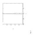
- Sample Bragg gratings in groups (A), (C), and (D)are then incubated in cortisol, and all sample Bragg gratings are re-measured with the Cary500. Only sample Bragg gratings in group (A) (the only group treated with anti-cortisol attachment and cortisol incubation) exhibit a red shift (approximately 1%), indicating the binding of cortisol to anti-cortisol thereby increases the mass in the pores and thus increasing the refractive index.
- FIG. 23exemplifies this shift when an anti-cortisol activated grating 2300 is incubated in cortisol 2310 .
- Two sample Bragg gratings from groups (A), (B), and (C)are subjected to a color test verification.
- the color testconsists of a competitive reaction between the antigen, i.e., cortisol, and an enzyme-conjugated antigen, i.e., anti-cortisol.
- Sample Bragg gratings in groups (A) and (C)are incubated in equal volumes of the antigen and the enzyme-conjugated antigen, while group (B) sample Bragg gratings are incubated in the enzyme-conjugated antigen only.
- Antigen and enzyme-conjugated antigen moleculesbind with present antibodies in proportion to their relative concentration.
- sample Bragg gratings with a higher proportion of enzyme-conjugated antigensexhibit a stronger color change, i.e., have a higher absorbance at 450 nm.
- the absorbance at 450 nmis inversely proportional to the concentration of antigen, i.e., cortisol, present, as exemplified in the test results in FIG. 24 .
- Sample Bragg grating 2410 incubated in cortisolexhibits a lower absorbance, i.e., some of the antibody sites are bound with cortisol and some with enzyme-conjugated antigen.
- Sample Bragg grating 2420 that was not treated with antibody attachmentshows the least absorbance, i.e., there are no sites for the enzyme-conjugated antigen to bind to and hence produces a color change.
Landscapes
- Health & Medical Sciences (AREA)
- Life Sciences & Earth Sciences (AREA)
- Immunology (AREA)
- Chemical & Material Sciences (AREA)
- Engineering & Computer Science (AREA)
- Physics & Mathematics (AREA)
- General Physics & Mathematics (AREA)
- Hematology (AREA)
- Biochemistry (AREA)
- General Health & Medical Sciences (AREA)
- Urology & Nephrology (AREA)
- Analytical Chemistry (AREA)
- Pathology (AREA)
- Biomedical Technology (AREA)
- Molecular Biology (AREA)
- Chemical Kinetics & Catalysis (AREA)
- Cell Biology (AREA)
- Microbiology (AREA)
- Biotechnology (AREA)
- Plasma & Fusion (AREA)
- Food Science & Technology (AREA)
- Medicinal Chemistry (AREA)
- Investigating Or Analysing Materials By Optical Means (AREA)
Abstract
Description
λB=2n(λr/2 sin θr)
where κ is the coupling constant of the grating and L is the grating thickness. The coupling constant is further given by κ=πn1/λB, where n1is the amplitude of the index modulation of the grating. For sufficiently thin gratings, the bandwidth is inversely proportional to the thickness. Thus, a thicker grating leads to a sharper reflection notch. The thicker grating also increases the diffraction efficiency. For sufficiently thick gratings, the bandwidth is directly proportional to κ. Thus, a small coupling constant κ (i.e., a small index modulation) also leads to a narrow spectral notch. Generally, a thick filter with a small index modulation yields a grating with high peak diffraction efficiency and a narrow spectral notch.
where npand nsare the refractive indices of the polymer and solution filling the pores, respectively. The parameters fcand α are determined by the phase separation of liquid crystal during the recording of the holographic grating. These are controlled by processing parameters such as recording intensity and total exposure, as well as material properties including liquid crystal concentration and concentrations of other recipe constituents, such as long chain aliphatic acids. With the refractive indices relatively fixed at npapproximately equal to 1.52 and nsapproximately equal to 1.33, the index modulation is directly controlled by the values of fcand α.
For example, let the Bragg wavelength be λB=850 nm for a grating with an average index n=1.5 and grating period Λ=283 nm. Thus, a spectral shift of ΔλB=1 nm is produced by Δn/n=ΔΛ/Λ=0.0012, i.e., Δn=0.00183, or ΔΛ=0.33 nm. A spectral shift of 1 nm produces a very significant change in the transmittance of the filter. Referring to
η=tanh2(κL)
where κ is the coupling coefficient and L is the filter thickness. The relative change Δη/η in diffraction efficiency is given by:
and
for changes in refractive index and grating period, respectively. Referring to
| TABLE 1 |
| Processing of Bragg Gratings for Gliadin-Anti-Gliadin Testsa |
| Phase | Phase | IgA | ||||
| Subset | Grating | I w/G | I w/o G | Incubationb | Phase II | Phase III |
| A | 3 | x | 6 U/mL | |||
| A | 5 | x | 6 U/mL | x | x | |
| A | 6 | X | 6 U/mL | x | x | |
| B | 2 | x | 31 U/mL | |||
| B | 8 | x | 31 U/mL | x | x | |
| B | 9 | X | 31 U/mL | x | ||
| Control | ||||||
| 1 | NA | x | x | |||
| a‘x’ denotes that part of the procedure that was used. | ||||||
| bUnits/milliliter (U/mL) of IgA are the concentration units used by the supplier of the test kit. | ||||||
Claims (35)
Priority Applications (2)
| Application Number | Priority Date | Filing Date | Title |
|---|---|---|---|
| US10/614,188US7619739B1 (en) | 2002-08-29 | 2003-07-08 | Detection and identification of biological agents using Bragg filters |
| US11/266,189US7186567B1 (en) | 2002-08-29 | 2005-11-04 | Device and method for detection and identification of biological agents |
Applications Claiming Priority (2)
| Application Number | Priority Date | Filing Date | Title |
|---|---|---|---|
| US40666502P | 2002-08-29 | 2002-08-29 | |
| US10/614,188US7619739B1 (en) | 2002-08-29 | 2003-07-08 | Detection and identification of biological agents using Bragg filters |
Related Child Applications (1)
| Application Number | Title | Priority Date | Filing Date |
|---|---|---|---|
| US11/266,189DivisionUS7186567B1 (en) | 2002-08-29 | 2005-11-04 | Device and method for detection and identification of biological agents |
Publications (1)
| Publication Number | Publication Date |
|---|---|
| US7619739B1true US7619739B1 (en) | 2009-11-17 |
Family
ID=37807110
Family Applications (2)
| Application Number | Title | Priority Date | Filing Date |
|---|---|---|---|
| US10/614,188Expired - Fee RelatedUS7619739B1 (en) | 2002-08-29 | 2003-07-08 | Detection and identification of biological agents using Bragg filters |
| US11/266,189Expired - LifetimeUS7186567B1 (en) | 2002-08-29 | 2005-11-04 | Device and method for detection and identification of biological agents |
Family Applications After (1)
| Application Number | Title | Priority Date | Filing Date |
|---|---|---|---|
| US11/266,189Expired - LifetimeUS7186567B1 (en) | 2002-08-29 | 2005-11-04 | Device and method for detection and identification of biological agents |
Country Status (1)
| Country | Link |
|---|---|
| US (2) | US7619739B1 (en) |
Cited By (60)
| Publication number | Priority date | Publication date | Assignee | Title |
|---|---|---|---|---|
| US20110194805A1 (en)* | 2010-02-11 | 2011-08-11 | The Hong Kong Polytechnic University | Fiber bragg grating in micro/nanofiber and method of producing the same |
| US20120154817A1 (en)* | 2009-05-05 | 2012-06-21 | Karlsruher Institut Fuer Technologie | Method for demonstrating the presence of molecules by means of optical gratings |
| US20120293797A1 (en)* | 2009-12-17 | 2012-11-22 | Universiteit Gent | Methods and systems for optical characterisation |
| US20130286196A1 (en)* | 2011-12-28 | 2013-10-31 | Faro Technologies, Inc. | Laser line probe that produces a line of light having a substantially even intensity distribution |
| US20160041384A1 (en)* | 2014-08-11 | 2016-02-11 | Steven Robbins | Waveguide eye tracking employing volume bragg grating |
| WO2016122577A1 (en)* | 2015-01-30 | 2016-08-04 | Hewlett-Packard Development Company, L.P. | Diagnostic chip |
| US20160238787A1 (en)* | 2015-02-13 | 2016-08-18 | Clarkson University | Forked grating coupler |
| US20160266029A1 (en)* | 2014-07-01 | 2016-09-15 | Octrolix Bv | Flow cytometry system and method |
| US9459451B2 (en) | 2013-12-26 | 2016-10-04 | Microsoft Technology Licensing, Llc | Eye tracking apparatus, method and system |
| US9494799B2 (en) | 2014-09-24 | 2016-11-15 | Microsoft Technology Licensing, Llc | Waveguide eye tracking employing switchable diffraction gratings |
| US10089516B2 (en) | 2013-07-31 | 2018-10-02 | Digilens, Inc. | Method and apparatus for contact image sensing |
| US10145533B2 (en) | 2005-11-11 | 2018-12-04 | Digilens, Inc. | Compact holographic illumination device |
| US10156681B2 (en) | 2015-02-12 | 2018-12-18 | Digilens Inc. | Waveguide grating device |
| US10185154B2 (en) | 2011-04-07 | 2019-01-22 | Digilens, Inc. | Laser despeckler based on angular diversity |
| US10209517B2 (en) | 2013-05-20 | 2019-02-19 | Digilens, Inc. | Holographic waveguide eye tracker |
| US10216061B2 (en) | 2012-01-06 | 2019-02-26 | Digilens, Inc. | Contact image sensor using switchable bragg gratings |
| US10234696B2 (en) | 2007-07-26 | 2019-03-19 | Digilens, Inc. | Optical apparatus for recording a holographic device and method of recording |
| US10241330B2 (en) | 2014-09-19 | 2019-03-26 | Digilens, Inc. | Method and apparatus for generating input images for holographic waveguide displays |
| US10330777B2 (en) | 2015-01-20 | 2019-06-25 | Digilens Inc. | Holographic waveguide lidar |
| US10359736B2 (en) | 2014-08-08 | 2019-07-23 | Digilens Inc. | Method for holographic mastering and replication |
| US10423222B2 (en) | 2014-09-26 | 2019-09-24 | Digilens Inc. | Holographic waveguide optical tracker |
| US10437051B2 (en) | 2012-05-11 | 2019-10-08 | Digilens Inc. | Apparatus for eye tracking |
| US10437064B2 (en) | 2015-01-12 | 2019-10-08 | Digilens Inc. | Environmentally isolated waveguide display |
| US10459145B2 (en) | 2015-03-16 | 2019-10-29 | Digilens Inc. | Waveguide device incorporating a light pipe |
| US10545346B2 (en) | 2017-01-05 | 2020-01-28 | Digilens Inc. | Wearable heads up displays |
| US10591756B2 (en) | 2015-03-31 | 2020-03-17 | Digilens Inc. | Method and apparatus for contact image sensing |
| US10642058B2 (en) | 2011-08-24 | 2020-05-05 | Digilens Inc. | Wearable data display |
| US10670876B2 (en) | 2011-08-24 | 2020-06-02 | Digilens Inc. | Waveguide laser illuminator incorporating a despeckler |
| US10678053B2 (en) | 2009-04-27 | 2020-06-09 | Digilens Inc. | Diffractive projection apparatus |
| US10690916B2 (en) | 2015-10-05 | 2020-06-23 | Digilens Inc. | Apparatus for providing waveguide displays with two-dimensional pupil expansion |
| US10690851B2 (en) | 2018-03-16 | 2020-06-23 | Digilens Inc. | Holographic waveguides incorporating birefringence control and methods for their fabrication |
| US10732569B2 (en) | 2018-01-08 | 2020-08-04 | Digilens Inc. | Systems and methods for high-throughput recording of holographic gratings in waveguide cells |
| US10859768B2 (en) | 2016-03-24 | 2020-12-08 | Digilens Inc. | Method and apparatus for providing a polarization selective holographic waveguide device |
| US10890707B2 (en) | 2016-04-11 | 2021-01-12 | Digilens Inc. | Holographic waveguide apparatus for structured light projection |
| US10914950B2 (en) | 2018-01-08 | 2021-02-09 | Digilens Inc. | Waveguide architectures and related methods of manufacturing |
| US10942430B2 (en) | 2017-10-16 | 2021-03-09 | Digilens Inc. | Systems and methods for multiplying the image resolution of a pixelated display |
| US10983340B2 (en) | 2016-02-04 | 2021-04-20 | Digilens Inc. | Holographic waveguide optical tracker |
| US20210296846A1 (en)* | 2020-03-18 | 2021-09-23 | Lumentum Operations Llc | Subsurface induced scattering centers |
| US11204540B2 (en) | 2009-10-09 | 2021-12-21 | Digilens Inc. | Diffractive waveguide providing a retinal image |
| US11307432B2 (en) | 2014-08-08 | 2022-04-19 | Digilens Inc. | Waveguide laser illuminator incorporating a Despeckler |
| US11340162B2 (en)* | 2017-10-18 | 2022-05-24 | Max-Planck-Gesellschaft Zur Foerderung Der Wissenschaften E.V. | Method and apparatus for comparing optical properties of two liquids |
| US11378732B2 (en) | 2019-03-12 | 2022-07-05 | DigLens Inc. | Holographic waveguide backlight and related methods of manufacturing |
| US11402801B2 (en) | 2018-07-25 | 2022-08-02 | Digilens Inc. | Systems and methods for fabricating a multilayer optical structure |
| US11442222B2 (en) | 2019-08-29 | 2022-09-13 | Digilens Inc. | Evacuated gratings and methods of manufacturing |
| US11448937B2 (en) | 2012-11-16 | 2022-09-20 | Digilens Inc. | Transparent waveguide display for tiling a display having plural optical powers using overlapping and offset FOV tiles |
| US11460621B2 (en) | 2012-04-25 | 2022-10-04 | Rockwell Collins, Inc. | Holographic wide angle display |
| US11480788B2 (en) | 2015-01-12 | 2022-10-25 | Digilens Inc. | Light field displays incorporating holographic waveguides |
| US11513350B2 (en) | 2016-12-02 | 2022-11-29 | Digilens Inc. | Waveguide device with uniform output illumination |
| US11543594B2 (en) | 2019-02-15 | 2023-01-03 | Digilens Inc. | Methods and apparatuses for providing a holographic waveguide display using integrated gratings |
| US11681143B2 (en) | 2019-07-29 | 2023-06-20 | Digilens Inc. | Methods and apparatus for multiplying the image resolution and field-of-view of a pixelated display |
| US11726332B2 (en) | 2009-04-27 | 2023-08-15 | Digilens Inc. | Diffractive projection apparatus |
| US11747568B2 (en) | 2019-06-07 | 2023-09-05 | Digilens Inc. | Waveguides incorporating transmissive and reflective gratings and related methods of manufacturing |
| US12092914B2 (en) | 2018-01-08 | 2024-09-17 | Digilens Inc. | Systems and methods for manufacturing waveguide cells |
| US12140764B2 (en) | 2019-02-15 | 2024-11-12 | Digilens Inc. | Wide angle waveguide display |
| US12158612B2 (en) | 2021-03-05 | 2024-12-03 | Digilens Inc. | Evacuated periodic structures and methods of manufacturing |
| US12210153B2 (en) | 2019-01-14 | 2025-01-28 | Digilens Inc. | Holographic waveguide display with light control layer |
| US12222499B2 (en) | 2020-12-21 | 2025-02-11 | Digilens Inc. | Eye glow suppression in waveguide based displays |
| US12306585B2 (en) | 2018-01-08 | 2025-05-20 | Digilens Inc. | Methods for fabricating optical waveguides |
| US12399326B2 (en) | 2021-01-07 | 2025-08-26 | Digilens Inc. | Grating structures for color waveguides |
| US12397477B2 (en) | 2019-02-05 | 2025-08-26 | Digilens Inc. | Methods for compensating for optical surface nonuniformity |
Families Citing this family (19)
| Publication number | Priority date | Publication date | Assignee | Title |
|---|---|---|---|---|
| GB0207943D0 (en)* | 2002-04-05 | 2002-05-15 | Univ Cambridge Tech | Sensors and their production |
| US20050018944A1 (en)* | 2003-07-25 | 2005-01-27 | Mozdy Eric J. | Polarization modulation interrogation of grating-coupled waveguide sensors |
| US8053245B1 (en)* | 2003-07-29 | 2011-11-08 | Nanotel Biotechnologies, Inc. | System and method for detecting biochemicals using hydrated substrates based on liquid crystal polymers |
| US7277604B2 (en)* | 2003-12-12 | 2007-10-02 | Lxsix Photonics Inc. | Method and apparatus for inducing an index of refraction change on a substrate sensitive to electromagnetic radiation |
| WO2005103652A1 (en)* | 2004-04-21 | 2005-11-03 | Ausbiochip Pty Ltd | Optoelectronic biochip |
| GB0617730D0 (en)* | 2006-09-08 | 2006-10-18 | Smart Holograms Ltd | Analyte detection |
| US7574082B2 (en)* | 2007-03-28 | 2009-08-11 | Verizon Services Organization Inc. | Optical power monitoring with robotically moved macro-bending |
| US7616851B1 (en)* | 2008-06-26 | 2009-11-10 | Lockheed Martin Corporation | Tunable wavelength filter device |
| WO2010030251A2 (en)* | 2008-09-15 | 2010-03-18 | Agency For Science, Technology And Research | Integrated optical sensors operating in the frequency domain |
| WO2011066071A1 (en)* | 2009-11-30 | 2011-06-03 | Corning Incorporated | Resonant-wavelength measurement method for label-independent scanning optical reader |
| WO2017001565A1 (en)* | 2015-06-30 | 2017-01-05 | Imec Vzw | Detection of fluid absorption spectrum |
| WO2017001566A1 (en)* | 2015-06-30 | 2017-01-05 | Imec Vzw | Absorption spectrum detection of a fluid |
| US20180117981A1 (en) | 2016-10-27 | 2018-05-03 | Alberto Daniel Lacaze | Vehicle Capable of Multiple Varieties of Locomotion |
| US11344884B2 (en)* | 2018-07-26 | 2022-05-31 | Boe Technology Group Co., Ltd. | Microfluidic apparatus, method of detecting substance in microfluidic apparatus, and spectrometer |
| US11619880B2 (en)* | 2019-05-17 | 2023-04-04 | The Regents Of The University Of Colorado | Holographic photopolymer compositions and composites |
| US11247089B2 (en)* | 2019-08-22 | 2022-02-15 | Robotic Research Opco, Llc | Chemical and biological warfare agent decontamination drone |
| JP7595259B2 (en)* | 2019-09-05 | 2024-12-06 | パナソニックIpマネジメント株式会社 | Light emitting device, light detection system, and vehicle |
| US20230088971A1 (en)* | 2021-09-21 | 2023-03-23 | Robert Bosch Gmbh | Soil samplers for monitoring soil conditions |
| CN115046926A (en)* | 2022-06-29 | 2022-09-13 | 湖南超亟检测技术有限责任公司 | Scanning identification method and scanning identification system based on grouped in-line gratings |
Citations (144)
| Publication number | Priority date | Publication date | Assignee | Title |
|---|---|---|---|---|
| CA544591A (en) | 1957-08-06 | Gabor Dennis | Optical apparatus | |
| US3580655A (en) | 1964-04-23 | 1971-05-25 | Battelle Development Corp | Wavefront reconstruction |
| US3658526A (en) | 1969-08-25 | 1972-04-25 | Du Pont | Hologram recording in photopolymerizable layers |
| US3667946A (en) | 1970-09-23 | 1972-06-06 | Holotron Corp | Surface treatment of photopolymer film used for recording holograms |
| US3758186A (en) | 1966-11-30 | 1973-09-11 | Battelle Development Corp | Method of copying holograms |
| US4003629A (en) | 1974-07-17 | 1977-01-18 | Siemens Aktiengesellschaft | Coupling device for light waves |
| US4006963A (en) | 1974-09-06 | 1977-02-08 | Siemens Aktiengesellschaft | Controllable, electro-optical grating coupler |
| US4018228A (en) | 1975-02-24 | 1977-04-19 | Goosen Carl C | Surgical punch apparatus |
| US4045124A (en) | 1975-02-25 | 1977-08-30 | Xerox Corporation | Bistable deflection system |
| US4124947A (en) | 1975-11-14 | 1978-11-14 | Adolf Kuhl | Graphic pattern or the like and method of producing the same |
| US4210132A (en) | 1978-07-26 | 1980-07-01 | The Kendall Company | Artificial sphincter |
| WO1981000668A1 (en) | 1979-09-07 | 1981-03-19 | A Jansen | Medical device for connecting two portions of the intestine,ancillary device for use therewith,and method for insertion of an intestinal button suture with the aid of this device |
| US4368736A (en) | 1980-11-17 | 1983-01-18 | Kaster Robert L | Anastomotic fitting |
| US4374371A (en) | 1980-01-17 | 1983-02-15 | Kearney-National, Inc. | Cadmium electric fuse |
| EP0087281A1 (en) | 1982-02-23 | 1983-08-31 | Fujitsu Limited | Method of constructing holograms |
| US4416540A (en) | 1981-11-23 | 1983-11-22 | Peter Nicholson | Apparatus and method for holographic contact copying |
| US4560249A (en) | 1982-04-16 | 1985-12-24 | Sumitomo Electric Industries, Ltd. | Method of forming diffraction gratings and optical branching filter elements produced thereby |
| US4688900A (en) | 1984-03-19 | 1987-08-25 | Kent State University | Light modulating material comprising a liquid crystal dispersion in a plastic matrix |
| US4728547A (en) | 1985-06-10 | 1988-03-01 | General Motors Corporation | Liquid crystal droplets dispersed in thin films of UV-curable polymers |
| US4809713A (en) | 1987-10-28 | 1989-03-07 | Joseph Grayzel | Catheter with magnetic fixation |
| US4810063A (en) | 1981-09-16 | 1989-03-07 | Manchester R & D Partnership | Enhanced scattering voltage sensitive encapsulated liquid crystal with light directing and interference layer features |
| US4818070A (en) | 1987-01-22 | 1989-04-04 | Asahi Glass Company Ltd. | Liquid crystal optical device using U.V.-cured polymer dispersions and process for its production |
| US4832424A (en) | 1982-09-30 | 1989-05-23 | Mcgrew Stephen P | White-light viewable, cylindrical holograms and method of spatially filtering wavefronts |
| US4844613A (en)* | 1986-11-03 | 1989-07-04 | Stc Plc | Optical surface plasmon sensor device |
| WO1989006264A1 (en) | 1987-12-28 | 1989-07-13 | Hughes Aircraft Company | Dispersion of liquid crystal droplets in a photopolymerized matrix, and devices made therefrom |
| US4856876A (en) | 1983-03-30 | 1989-08-15 | Manchester R & D Partnership | Fluorescent colored encapsulated liquid crystal apparatus using enhanced scattering |
| US4857425A (en) | 1986-06-30 | 1989-08-15 | Holtronic Technologies Limited | Manufacture of integrated circuits using holographic techniques |
| GB2222696A (en) | 1988-07-09 | 1990-03-14 | Exitech Ltd | Holographic diffraction gratings |
| US4923269A (en) | 1987-01-29 | 1990-05-08 | British Telecommunications Public Limited Company | Bidirectional optical space switch |
| US4929240A (en) | 1983-12-01 | 1990-05-29 | University Of New Mexico | Surgical clip and applier |
| US4930674A (en) | 1989-02-24 | 1990-06-05 | Abiomed, Inc. | Surgical stapler |
| US4938568A (en) | 1988-01-05 | 1990-07-03 | Hughes Aircraft Company | Polymer dispersed liquid crystal film devices, and method of forming the same |
| US4942102A (en) | 1988-01-15 | 1990-07-17 | E. I. Du Pont De Nemours And Company | Holographic optical elements having a reflection hologram formed in a photopolymer |
| US4983176A (en) | 1989-03-06 | 1991-01-08 | University Of New Mexico | Deformable plastic surgical clip |
| SU1635966A1 (en) | 1988-03-17 | 1991-03-23 | Свердловский государственный медицинский институт | Method for anastomosis of hollow organs |
| US5003386A (en) | 1988-12-20 | 1991-03-26 | Ilford Limited | Preparation of a copy hologram with a light modulating array derived from a master hologram |
| EP0422689A2 (en) | 1986-02-03 | 1991-04-17 | Mountpelier Investments, S.A. | Catheter |
| US5011624A (en) | 1987-12-30 | 1991-04-30 | Yamagishi Frederick G | Acrylate polymer-dispersed liquid crystal material and device made therefrom |
| US5014709A (en) | 1989-06-13 | 1991-05-14 | Biologic Systems Corp. | Method and apparatus for high resolution holographic imaging of biological tissue |
| US5015249A (en) | 1989-12-26 | 1991-05-14 | Nakao Naomi L | Endoscopic stapling device and method |
| JPH03188479A (en) | 1989-12-18 | 1991-08-16 | Fujitsu Ltd | How to replicate a reflection hologram |
| US5047040A (en) | 1987-11-05 | 1991-09-10 | Devices For Vascular Intervention, Inc. | Atherectomy device and method |
| US5084203A (en) | 1991-03-13 | 1992-01-28 | Hoechst Celanese Corp. | Light transmissive liquid crystalline composite exhibiting a high Kerr effect |
| US5096282A (en) | 1988-01-05 | 1992-03-17 | Hughes Aircraft Co. | Polymer dispersed liquid crystal film devices |
| US5105298A (en) | 1989-07-12 | 1992-04-14 | Board Of Trustees, Leland Stanford Jr. University | Birefringent structures formed by photo-exposure of polymer films and method for fabrication thereof |
| US5136666A (en) | 1991-08-06 | 1992-08-04 | The University Of Colorado Foundation, Inc. | Fiber optic communication method and apparatus providing mode multiplexing and holographic demultiplexing |
| US5144690A (en) | 1990-12-03 | 1992-09-01 | Corning Incorporated | Optical fiber sensor with localized sensing regions |
| US5166813A (en) | 1988-05-31 | 1992-11-24 | Nygene Corporation | Optical evaluation using a hologram barrier filter |
| US5170925A (en) | 1991-03-18 | 1992-12-15 | Ethicon, Inc. | Laparoscopic stapler with knife means |
| US5174276A (en) | 1988-11-18 | 1992-12-29 | Hillway Surgical Limited | Endoscope device for applying an aneurysm clip |
| US5182180A (en) | 1991-08-27 | 1993-01-26 | E. I. Du Pont De Nemours And Company | Dry film process for altering the wavelength of response of holograms |
| US5182665A (en) | 1990-09-07 | 1993-01-26 | Displaytech, Inc. | Diffractive light modulator |
| US5188638A (en) | 1992-02-06 | 1993-02-23 | Tzakis Andreas G | Apparatus and method for preforming anastomosis fastener securement of hollow organs |
| US5198912A (en) | 1990-01-12 | 1993-03-30 | Polaroid Corporation | Volume phase hologram with liquid crystal in microvoids between fringes |
| US5210630A (en) | 1989-10-18 | 1993-05-11 | U.S. Philips Corporation | Liquid-crystal display device |
| US5227859A (en) | 1990-12-04 | 1993-07-13 | Grumman Aerospace Corporation | Passive coherent radiation detection system |
| US5227906A (en) | 1989-03-09 | 1993-07-13 | Canon Kabushiki Kaisha | Optical switch array capable of bidirectional signal transfer between a plurality of terminals |
| US5234447A (en) | 1990-08-28 | 1993-08-10 | Robert L. Kaster | Side-to-end vascular anastomotic staple apparatus |
| US5235445A (en) | 1991-04-17 | 1993-08-10 | Ag-Technology Co., Ltd. | Liquid crystal optical element with liquid crystal in polymer matrix with particular modulus of elasticity |
| US5240636A (en) | 1988-04-11 | 1993-08-31 | Kent State University | Light modulating materials comprising a liquid crystal microdroplets dispersed in a birefringent polymeric matri method of making light modulating materials |
| US5258008A (en) | 1992-07-29 | 1993-11-02 | Wilk Peter J | Surgical stapling device and associated method |
| US5264950A (en) | 1992-01-06 | 1993-11-23 | Kent State University | Light modulating device with polarizer and liquid crystal interspersed as spherical or randomly distorted droplets in isotropic polymer |
| US5270843A (en) | 1992-08-31 | 1993-12-14 | Jiansheng Wang | Directly formed polymer dispersed liquid crystal light shutter displays |
| US5272550A (en) | 1991-10-11 | 1993-12-21 | International Business Machines Corporation | Hologram system |
| US5291317A (en) | 1990-07-12 | 1994-03-01 | Applied Holographics Corporation | Holographic diffraction grating patterns and methods for creating the same |
| WO1994004958A1 (en) | 1992-08-25 | 1994-03-03 | Merck Patent Gmbh | Paper white pdlc system |
| US5299289A (en) | 1991-06-11 | 1994-03-29 | Matsushita Electric Industrial Co., Ltd. | Polymer dispersed liquid crystal panel with diffraction grating |
| US5303322A (en) | 1992-03-23 | 1994-04-12 | Nioptics Corporation | Tapered multilayer luminaire devices |
| US5313317A (en) | 1991-10-09 | 1994-05-17 | Nippondenso Co., Ltd. | Hologram |
| US5323251A (en) | 1991-11-01 | 1994-06-21 | Merck Patent Gesellschaft Mit Beschrankter Haftung | Electrooptical liquid crystal system |
| US5328800A (en) | 1991-05-07 | 1994-07-12 | Fuji Photo Film Co., Ltd. | Color image forming method using silver halide, reducing agent, polymerizable compound and colorant |
| JPH06190185A (en) | 1992-10-22 | 1994-07-12 | Zanussi Elettrodomestici Spa | Washing machine provided with mutually linked semi-shell type casing |
| US5330486A (en) | 1992-07-29 | 1994-07-19 | Wilk Peter J | Laparoscopic or endoscopic anastomosis technique and associated instruments |
| US5330264A (en) | 1991-05-01 | 1994-07-19 | Nippondenso Co., Ltd. | Method and apparatus for copying and manufacturing hologram plate |
| US5354498A (en) | 1990-03-16 | 1994-10-11 | Fuji Xerox Co., Ltd. | Phase separation liquid crystal polymer |
| US5356557A (en) | 1991-03-13 | 1994-10-18 | Merck Patent Gesellschaft Mit Beschrankter Haftung | Electrooptical system |
| US5363228A (en) | 1993-03-05 | 1994-11-08 | General Electric Company | Optical device with spatial light modulators for switching arbitrarily polarized light |
| US5366462A (en) | 1990-08-28 | 1994-11-22 | Robert L. Kaster | Method of side-to-end vascular anastomotic stapling |
| US5377008A (en)* | 1990-09-20 | 1994-12-27 | Battelle Memorial Institute | Integrated optical compensating refractometer apparatus |
| US5376095A (en) | 1993-11-04 | 1994-12-27 | Ethicon Endo-Surgery | Endoscopic multi-fire flat stapler with low profile |
| US5384067A (en) | 1991-05-02 | 1995-01-24 | Kent State University | Grey scale liquid crystal material |
| WO1995017127A1 (en) | 1993-12-23 | 1995-06-29 | Oticon A/S | Method and instrument for establishing the receiving site of a coronary artery bypass graft |
| EP0672386A1 (en) | 1994-03-10 | 1995-09-20 | SURGICAL SYSTEMS & INSTRUMENTS Inc. | Lumen tracking atherectomy system |
| DE4408746A1 (en) | 1994-03-15 | 1995-09-21 | Medolas Ges Fuer Medizintechni | Laser catheter for bypass surgery |
| US5453338A (en) | 1992-03-31 | 1995-09-26 | Dai Nippon Printing Co., Ltd. | Hologram and method of and apparatus for producing the same |
| US5471326A (en) | 1993-04-30 | 1995-11-28 | Northrop Grumman Corporation | Holographic laser scanner and rangefinder |
| US5488681A (en) | 1994-09-09 | 1996-01-30 | Deacon Research | Method for controllable optical power splitting |
| US5499118A (en) | 1994-08-31 | 1996-03-12 | Hughes Aircraft Company | System for copying multiple holograms |
| US5529861A (en) | 1993-07-14 | 1996-06-25 | Tamarack Storage Devices | Method for enhancing the utility of a photopolymer recording media for holographic data recording |
| US5544268A (en) | 1994-09-09 | 1996-08-06 | Deacon Research | Display panel with electrically-controlled waveguide-routing |
| US5547786A (en) | 1992-10-06 | 1996-08-20 | Northrop Grumman Corporation | System and method of fabricating multiple holographic elements |
| US5593615A (en) | 1994-04-29 | 1997-01-14 | Minnesota Mining And Manufacturing Company | Light modulating device having a matrix prepared from acid reactants |
| US5641426A (en) | 1994-04-29 | 1997-06-24 | Minnesota Mining And Manufacturing Company | Light modulating device having a vinyl ether-based matrix |
| US5648857A (en) | 1994-02-18 | 1997-07-15 | Nippondenso Co., Ltd. | Manufacturing method for hologram which can prevent the formation of ghant holograms due to noise light |
| WO1997027519A1 (en) | 1996-01-29 | 1997-07-31 | Foster-Miller, Inc. | Optical components containing complex diffraction gratings and methods for the fabrication thereof |
| US5661533A (en) | 1995-05-19 | 1997-08-26 | Advanced Display Systems, Inc. | Ultra fast response, multistable reflective cholesteric liquid crystal displays |
| US5661577A (en) | 1990-04-06 | 1997-08-26 | University Of Southern California | Incoherent/coherent double angularly multiplexed volume holographic optical elements |
| US5680233A (en) | 1994-04-21 | 1997-10-21 | Reveo, Inc. | Image display systems having direct and projection viewing modes |
| US5682214A (en) | 1990-04-05 | 1997-10-28 | Seiko Epson Corporation | Optical apparatus for controlling the wavefront of a coherent light |
| US5695682A (en) | 1991-05-02 | 1997-12-09 | Kent State University | Liquid crystalline light modulating device and material |
| US5698343A (en) | 1994-07-05 | 1997-12-16 | The United States Of America As Represented By The Secretary Of The Air Force | Laser wavelength detection and energy dosimetry badge |
| US5698134A (en) | 1991-09-13 | 1997-12-16 | Merck Kgaa | Electrooptical system |
| US5706375A (en) | 1996-09-10 | 1998-01-06 | Jds Fitel Inc. | Variable-attenuation tunable optical router |
| WO1998004650A1 (en) | 1996-07-12 | 1998-02-05 | Science Applications International Corporation | Switchable volume hologram materials and devices |
| US5725970A (en) | 1994-11-07 | 1998-03-10 | E. I. Du Pont De Nemours And Company | Broad band reflection holograms and a dry process for making same |
| US5731853A (en) | 1995-02-24 | 1998-03-24 | Matsushita Electric Industrial Co., Ltd. | Display device |
| US5734485A (en) | 1995-04-25 | 1998-03-31 | Rocky Research | Large display composite holograms and methods |
| US5748272A (en) | 1993-02-22 | 1998-05-05 | Nippon Telegraph And Telephone Corporation | Method for making an optical device using a laser beam interference pattern |
| GB2281566B (en) | 1993-09-02 | 1998-05-13 | Merck Patent Gmbh | Composite material |
| US5771320A (en) | 1996-04-30 | 1998-06-23 | Wavefront Research, Inc. | Optical switching and routing system |
| EP0856768A2 (en) | 1997-01-31 | 1998-08-05 | Xerox Corporation | Broadband reflective display, and methods of forming the same |
| EP0856766A2 (en) | 1997-01-31 | 1998-08-05 | Xerox Corporation | Holographically formed reflective display, liquid crystal display and projection system and methods of forming the same |
| EP0856765A1 (en) | 1997-01-31 | 1998-08-05 | Xerox Corporation | Reflective-type liquid crystal display and methods of forming the same |
| GB2292745B (en) | 1994-09-02 | 1998-08-19 | Merck Patent Gmbh | Composite material |
| EP0867749A2 (en) | 1997-03-27 | 1998-09-30 | Xerox Corporation | Liquid crystal display |
| US5832148A (en) | 1995-12-20 | 1998-11-03 | California Institute Of Technology | Electrically controlled wavelength multiplexing waveguide filter |
| JPH10319237A (en) | 1997-05-22 | 1998-12-04 | Fuji Xerox Co Ltd | Volume hologram optical element |
| US5852504A (en) | 1992-08-21 | 1998-12-22 | Fujitsu Limited | Stereoscopic display method of hologram and its forming method and its stereoscopic display apparatus |
| US5862214A (en) | 1995-11-09 | 1999-01-19 | Lucent Technologies Inc. | Low cost adjustable base stand |
| US5864641A (en)* | 1997-04-11 | 1999-01-26 | F&S, Inc. | Optical fiber long period sensor having a reactive coating |
| WO1999009440A1 (en) | 1997-08-13 | 1999-02-25 | Foster-Miller, Inc. | Switchable optical components |
| US5915051A (en) | 1997-01-21 | 1999-06-22 | Massascusetts Institute Of Technology | Wavelength-selective optical add/drop switch |
| US5917607A (en)* | 1996-04-25 | 1999-06-29 | Fuji Photo Film Co., Ltd. | Surface plasmon sensor for multiple channel analysis |
| US5930011A (en) | 1994-06-10 | 1999-07-27 | E. I. Du Pont De Nemours And Company | Holographic Multicolor optical elements for use in liquid crystal displays and methods of making the elements |
| US5937115A (en) | 1997-02-12 | 1999-08-10 | Foster-Miller, Inc. | Switchable optical components/structures and methods for the fabrication thereof |
| US5989923A (en) | 1994-03-28 | 1999-11-23 | Btg International Limited | Hologram containing sensor |
| US6115152A (en) | 1998-09-14 | 2000-09-05 | Digilens, Inc. | Holographic illumination system |
| US6130748A (en) | 1996-03-05 | 2000-10-10 | Forschungszentrum Julich Gmbh | Chemical sensor based on porous silicon |
| US6172778B1 (en) | 1997-01-27 | 2001-01-09 | Yeda Research & Development Co. Ltd. Of Weizmann Institute Of Science | Compact optical crossbar switch |
| US6187599B1 (en) | 1996-11-06 | 2001-02-13 | University Of Pittsburgh | Polymerized crystalline colloidal arrays |
| US6239876B1 (en)* | 1997-07-29 | 2001-05-29 | Fräunhofer-Gesellschaft zur Förderung der Angewandten Forschung e.V. | Optical detector device |
| US20010030741A1 (en)* | 1997-09-18 | 2001-10-18 | Herron James N. | Diagnostic device and method |
| US20010040679A1 (en) | 1998-05-29 | 2001-11-15 | Yuji Kawabata | Surface plasmon resonance sensor apparatus using surface emitting laser |
| US20010044119A1 (en) | 1997-09-05 | 2001-11-22 | Ghadiri M. Reza | Porous semiconductor-based optical interferometric sensor |
| US20020003627A1 (en) | 2000-03-13 | 2002-01-10 | Rieder Ronald J. | Doubly-differential interferometer and method for evanescent wave surface detection |
| US6395558B1 (en) | 1996-08-29 | 2002-05-28 | Zeptosens Ag | Optical chemical/biochemical sensor |
| US6493090B1 (en)* | 1998-01-23 | 2002-12-10 | Torsana A/S | Detection of a substance by refractive index change |
| US20030146109A1 (en)* | 2002-01-25 | 2003-08-07 | The Regents Of The University Of California | Porous thin film time-varying reflectivity analysis of samples |
| US6689316B1 (en) | 1998-05-29 | 2004-02-10 | Cambridge University Technical Services, Ltd. | Holographic sensors and their production |
| US20040045932A1 (en)* | 2002-06-04 | 2004-03-11 | Lake Shore Cryotronics, Inc. | Method of manufacturing a spectral filter for green and shorter wavelengths |
| US6723516B1 (en)* | 1995-01-31 | 2004-04-20 | Agilent Technologies, Inc. | Method for continuously detecting the presence and quantity of analytes in a flowing liquid stream |
| US6771857B1 (en)* | 1997-02-12 | 2004-08-03 | Hoya Corporation | Switchable optical components |
| US6781696B1 (en)* | 1999-10-06 | 2004-08-24 | The Board Of Regents For Oklahoma State University | Apparatus and method for a microsphere whispering-gallery mode evanescent-wave sensor |
| US6791691B2 (en)* | 2001-10-19 | 2004-09-14 | Fuji Photo Film Co., Ltd. | Measuring method and apparatus using attenuation in total internal reflection |
- 2003
- 2003-07-08USUS10/614,188patent/US7619739B1/ennot_activeExpired - Fee Related
- 2005
- 2005-11-04USUS11/266,189patent/US7186567B1/ennot_activeExpired - Lifetime
Patent Citations (150)
| Publication number | Priority date | Publication date | Assignee | Title |
|---|---|---|---|---|
| CA544591A (en) | 1957-08-06 | Gabor Dennis | Optical apparatus | |
| US3580655A (en) | 1964-04-23 | 1971-05-25 | Battelle Development Corp | Wavefront reconstruction |
| US3758186A (en) | 1966-11-30 | 1973-09-11 | Battelle Development Corp | Method of copying holograms |
| US3658526A (en) | 1969-08-25 | 1972-04-25 | Du Pont | Hologram recording in photopolymerizable layers |
| US3667946A (en) | 1970-09-23 | 1972-06-06 | Holotron Corp | Surface treatment of photopolymer film used for recording holograms |
| US4003629A (en) | 1974-07-17 | 1977-01-18 | Siemens Aktiengesellschaft | Coupling device for light waves |
| US4006963A (en) | 1974-09-06 | 1977-02-08 | Siemens Aktiengesellschaft | Controllable, electro-optical grating coupler |
| US4018228A (en) | 1975-02-24 | 1977-04-19 | Goosen Carl C | Surgical punch apparatus |
| US4045124A (en) | 1975-02-25 | 1977-08-30 | Xerox Corporation | Bistable deflection system |
| US4124947A (en) | 1975-11-14 | 1978-11-14 | Adolf Kuhl | Graphic pattern or the like and method of producing the same |
| US4210132A (en) | 1978-07-26 | 1980-07-01 | The Kendall Company | Artificial sphincter |
| WO1981000668A1 (en) | 1979-09-07 | 1981-03-19 | A Jansen | Medical device for connecting two portions of the intestine,ancillary device for use therewith,and method for insertion of an intestinal button suture with the aid of this device |
| US4374371A (en) | 1980-01-17 | 1983-02-15 | Kearney-National, Inc. | Cadmium electric fuse |
| US4368736A (en) | 1980-11-17 | 1983-01-18 | Kaster Robert L | Anastomotic fitting |
| US4810063A (en) | 1981-09-16 | 1989-03-07 | Manchester R & D Partnership | Enhanced scattering voltage sensitive encapsulated liquid crystal with light directing and interference layer features |
| US4416540A (en) | 1981-11-23 | 1983-11-22 | Peter Nicholson | Apparatus and method for holographic contact copying |
| EP0087281A1 (en) | 1982-02-23 | 1983-08-31 | Fujitsu Limited | Method of constructing holograms |
| US4560249A (en) | 1982-04-16 | 1985-12-24 | Sumitomo Electric Industries, Ltd. | Method of forming diffraction gratings and optical branching filter elements produced thereby |
| US4673241A (en) | 1982-04-16 | 1987-06-16 | Sumitomo Electric Industries, Ltd. | Diffraction gratings and optical branching filter elements |
| US4832424A (en) | 1982-09-30 | 1989-05-23 | Mcgrew Stephen P | White-light viewable, cylindrical holograms and method of spatially filtering wavefronts |
| US4856876A (en) | 1983-03-30 | 1989-08-15 | Manchester R & D Partnership | Fluorescent colored encapsulated liquid crystal apparatus using enhanced scattering |
| US4929240A (en) | 1983-12-01 | 1990-05-29 | University Of New Mexico | Surgical clip and applier |
| US4688900A (en) | 1984-03-19 | 1987-08-25 | Kent State University | Light modulating material comprising a liquid crystal dispersion in a plastic matrix |
| US4728547A (en) | 1985-06-10 | 1988-03-01 | General Motors Corporation | Liquid crystal droplets dispersed in thin films of UV-curable polymers |
| EP0422689A2 (en) | 1986-02-03 | 1991-04-17 | Mountpelier Investments, S.A. | Catheter |
| US4857425A (en) | 1986-06-30 | 1989-08-15 | Holtronic Technologies Limited | Manufacture of integrated circuits using holographic techniques |
| US4844613A (en)* | 1986-11-03 | 1989-07-04 | Stc Plc | Optical surface plasmon sensor device |
| US4818070A (en) | 1987-01-22 | 1989-04-04 | Asahi Glass Company Ltd. | Liquid crystal optical device using U.V.-cured polymer dispersions and process for its production |
| US4923269A (en) | 1987-01-29 | 1990-05-08 | British Telecommunications Public Limited Company | Bidirectional optical space switch |
| US4809713A (en) | 1987-10-28 | 1989-03-07 | Joseph Grayzel | Catheter with magnetic fixation |
| US5047040A (en) | 1987-11-05 | 1991-09-10 | Devices For Vascular Intervention, Inc. | Atherectomy device and method |
| WO1989006264A1 (en) | 1987-12-28 | 1989-07-13 | Hughes Aircraft Company | Dispersion of liquid crystal droplets in a photopolymerized matrix, and devices made therefrom |
| US4891152A (en) | 1987-12-28 | 1990-01-02 | Hughes Aircraft Company | Dispersion of liquid crystal droplets in a photopolymerized matrix and devices made therefrom |
| US5011624A (en) | 1987-12-30 | 1991-04-30 | Yamagishi Frederick G | Acrylate polymer-dispersed liquid crystal material and device made therefrom |
| US5096282A (en) | 1988-01-05 | 1992-03-17 | Hughes Aircraft Co. | Polymer dispersed liquid crystal film devices |
| US4938568A (en) | 1988-01-05 | 1990-07-03 | Hughes Aircraft Company | Polymer dispersed liquid crystal film devices, and method of forming the same |
| US4942102A (en) | 1988-01-15 | 1990-07-17 | E. I. Du Pont De Nemours And Company | Holographic optical elements having a reflection hologram formed in a photopolymer |
| SU1635966A1 (en) | 1988-03-17 | 1991-03-23 | Свердловский государственный медицинский институт | Method for anastomosis of hollow organs |
| US5240636A (en) | 1988-04-11 | 1993-08-31 | Kent State University | Light modulating materials comprising a liquid crystal microdroplets dispersed in a birefringent polymeric matri method of making light modulating materials |
| US5166813A (en) | 1988-05-31 | 1992-11-24 | Nygene Corporation | Optical evaluation using a hologram barrier filter |
| GB2222696A (en) | 1988-07-09 | 1990-03-14 | Exitech Ltd | Holographic diffraction gratings |
| US5174276A (en) | 1988-11-18 | 1992-12-29 | Hillway Surgical Limited | Endoscope device for applying an aneurysm clip |
| US5003386A (en) | 1988-12-20 | 1991-03-26 | Ilford Limited | Preparation of a copy hologram with a light modulating array derived from a master hologram |
| US4930674A (en) | 1989-02-24 | 1990-06-05 | Abiomed, Inc. | Surgical stapler |
| US4983176A (en) | 1989-03-06 | 1991-01-08 | University Of New Mexico | Deformable plastic surgical clip |
| US5227906A (en) | 1989-03-09 | 1993-07-13 | Canon Kabushiki Kaisha | Optical switch array capable of bidirectional signal transfer between a plurality of terminals |
| US5014709A (en) | 1989-06-13 | 1991-05-14 | Biologic Systems Corp. | Method and apparatus for high resolution holographic imaging of biological tissue |
| US5105298A (en) | 1989-07-12 | 1992-04-14 | Board Of Trustees, Leland Stanford Jr. University | Birefringent structures formed by photo-exposure of polymer films and method for fabrication thereof |
| US5210630A (en) | 1989-10-18 | 1993-05-11 | U.S. Philips Corporation | Liquid-crystal display device |
| JPH03188479A (en) | 1989-12-18 | 1991-08-16 | Fujitsu Ltd | How to replicate a reflection hologram |
| US5015249A (en) | 1989-12-26 | 1991-05-14 | Nakao Naomi L | Endoscopic stapling device and method |
| US5198912A (en) | 1990-01-12 | 1993-03-30 | Polaroid Corporation | Volume phase hologram with liquid crystal in microvoids between fringes |
| US5354498A (en) | 1990-03-16 | 1994-10-11 | Fuji Xerox Co., Ltd. | Phase separation liquid crystal polymer |
| US5682214A (en) | 1990-04-05 | 1997-10-28 | Seiko Epson Corporation | Optical apparatus for controlling the wavefront of a coherent light |
| US5661577A (en) | 1990-04-06 | 1997-08-26 | University Of Southern California | Incoherent/coherent double angularly multiplexed volume holographic optical elements |
| US5291317A (en) | 1990-07-12 | 1994-03-01 | Applied Holographics Corporation | Holographic diffraction grating patterns and methods for creating the same |
| US5234447A (en) | 1990-08-28 | 1993-08-10 | Robert L. Kaster | Side-to-end vascular anastomotic staple apparatus |
| US5366462A (en) | 1990-08-28 | 1994-11-22 | Robert L. Kaster | Method of side-to-end vascular anastomotic stapling |
| US5182665A (en) | 1990-09-07 | 1993-01-26 | Displaytech, Inc. | Diffractive light modulator |
| US5377008A (en)* | 1990-09-20 | 1994-12-27 | Battelle Memorial Institute | Integrated optical compensating refractometer apparatus |
| US5144690A (en) | 1990-12-03 | 1992-09-01 | Corning Incorporated | Optical fiber sensor with localized sensing regions |
| US5227859A (en) | 1990-12-04 | 1993-07-13 | Grumman Aerospace Corporation | Passive coherent radiation detection system |
| US5356557A (en) | 1991-03-13 | 1994-10-18 | Merck Patent Gesellschaft Mit Beschrankter Haftung | Electrooptical system |
| US5084203A (en) | 1991-03-13 | 1992-01-28 | Hoechst Celanese Corp. | Light transmissive liquid crystalline composite exhibiting a high Kerr effect |
| US5170925A (en) | 1991-03-18 | 1992-12-15 | Ethicon, Inc. | Laparoscopic stapler with knife means |
| US5235445A (en) | 1991-04-17 | 1993-08-10 | Ag-Technology Co., Ltd. | Liquid crystal optical element with liquid crystal in polymer matrix with particular modulus of elasticity |
| US5330264A (en) | 1991-05-01 | 1994-07-19 | Nippondenso Co., Ltd. | Method and apparatus for copying and manufacturing hologram plate |
| US5384067A (en) | 1991-05-02 | 1995-01-24 | Kent State University | Grey scale liquid crystal material |
| US5695682A (en) | 1991-05-02 | 1997-12-09 | Kent State University | Liquid crystalline light modulating device and material |
| US5328800A (en) | 1991-05-07 | 1994-07-12 | Fuji Photo Film Co., Ltd. | Color image forming method using silver halide, reducing agent, polymerizable compound and colorant |
| US5299289A (en) | 1991-06-11 | 1994-03-29 | Matsushita Electric Industrial Co., Ltd. | Polymer dispersed liquid crystal panel with diffraction grating |
| US5136666A (en) | 1991-08-06 | 1992-08-04 | The University Of Colorado Foundation, Inc. | Fiber optic communication method and apparatus providing mode multiplexing and holographic demultiplexing |
| US5182180A (en) | 1991-08-27 | 1993-01-26 | E. I. Du Pont De Nemours And Company | Dry film process for altering the wavelength of response of holograms |
| US5698134A (en) | 1991-09-13 | 1997-12-16 | Merck Kgaa | Electrooptical system |
| US5313317A (en) | 1991-10-09 | 1994-05-17 | Nippondenso Co., Ltd. | Hologram |
| US5272550A (en) | 1991-10-11 | 1993-12-21 | International Business Machines Corporation | Hologram system |
| US5323251A (en) | 1991-11-01 | 1994-06-21 | Merck Patent Gesellschaft Mit Beschrankter Haftung | Electrooptical liquid crystal system |
| US5264950A (en) | 1992-01-06 | 1993-11-23 | Kent State University | Light modulating device with polarizer and liquid crystal interspersed as spherical or randomly distorted droplets in isotropic polymer |
| US5188638A (en) | 1992-02-06 | 1993-02-23 | Tzakis Andreas G | Apparatus and method for preforming anastomosis fastener securement of hollow organs |
| US5303322A (en) | 1992-03-23 | 1994-04-12 | Nioptics Corporation | Tapered multilayer luminaire devices |
| US5453338A (en) | 1992-03-31 | 1995-09-26 | Dai Nippon Printing Co., Ltd. | Hologram and method of and apparatus for producing the same |
| US5330486A (en) | 1992-07-29 | 1994-07-19 | Wilk Peter J | Laparoscopic or endoscopic anastomosis technique and associated instruments |
| US5258008A (en) | 1992-07-29 | 1993-11-02 | Wilk Peter J | Surgical stapling device and associated method |
| US5852504A (en) | 1992-08-21 | 1998-12-22 | Fujitsu Limited | Stereoscopic display method of hologram and its forming method and its stereoscopic display apparatus |
| WO1994004958A1 (en) | 1992-08-25 | 1994-03-03 | Merck Patent Gmbh | Paper white pdlc system |
| US5270843A (en) | 1992-08-31 | 1993-12-14 | Jiansheng Wang | Directly formed polymer dispersed liquid crystal light shutter displays |
| US5547786A (en) | 1992-10-06 | 1996-08-20 | Northrop Grumman Corporation | System and method of fabricating multiple holographic elements |
| JPH06190185A (en) | 1992-10-22 | 1994-07-12 | Zanussi Elettrodomestici Spa | Washing machine provided with mutually linked semi-shell type casing |
| US5751452A (en) | 1993-02-22 | 1998-05-12 | Nippon Telegraph And Telephone Corporation | Optical devices with high polymer material and method of forming the same |
| US5748272A (en) | 1993-02-22 | 1998-05-05 | Nippon Telegraph And Telephone Corporation | Method for making an optical device using a laser beam interference pattern |
| US5363228A (en) | 1993-03-05 | 1994-11-08 | General Electric Company | Optical device with spatial light modulators for switching arbitrarily polarized light |
| US5471326A (en) | 1993-04-30 | 1995-11-28 | Northrop Grumman Corporation | Holographic laser scanner and rangefinder |
| US5529861A (en) | 1993-07-14 | 1996-06-25 | Tamarack Storage Devices | Method for enhancing the utility of a photopolymer recording media for holographic data recording |
| GB2281566B (en) | 1993-09-02 | 1998-05-13 | Merck Patent Gmbh | Composite material |
| US5376095A (en) | 1993-11-04 | 1994-12-27 | Ethicon Endo-Surgery | Endoscopic multi-fire flat stapler with low profile |
| WO1995017127A1 (en) | 1993-12-23 | 1995-06-29 | Oticon A/S | Method and instrument for establishing the receiving site of a coronary artery bypass graft |
| US5648857A (en) | 1994-02-18 | 1997-07-15 | Nippondenso Co., Ltd. | Manufacturing method for hologram which can prevent the formation of ghant holograms due to noise light |
| EP0672386A1 (en) | 1994-03-10 | 1995-09-20 | SURGICAL SYSTEMS & INSTRUMENTS Inc. | Lumen tracking atherectomy system |
| DE4408746A1 (en) | 1994-03-15 | 1995-09-21 | Medolas Ges Fuer Medizintechni | Laser catheter for bypass surgery |
| US5989923A (en) | 1994-03-28 | 1999-11-23 | Btg International Limited | Hologram containing sensor |
| US5680233A (en) | 1994-04-21 | 1997-10-21 | Reveo, Inc. | Image display systems having direct and projection viewing modes |
| US5593615A (en) | 1994-04-29 | 1997-01-14 | Minnesota Mining And Manufacturing Company | Light modulating device having a matrix prepared from acid reactants |
| US5641426A (en) | 1994-04-29 | 1997-06-24 | Minnesota Mining And Manufacturing Company | Light modulating device having a vinyl ether-based matrix |
| US5930011A (en) | 1994-06-10 | 1999-07-27 | E. I. Du Pont De Nemours And Company | Holographic Multicolor optical elements for use in liquid crystal displays and methods of making the elements |
| US5698343A (en) | 1994-07-05 | 1997-12-16 | The United States Of America As Represented By The Secretary Of The Air Force | Laser wavelength detection and energy dosimetry badge |
| US5499118A (en) | 1994-08-31 | 1996-03-12 | Hughes Aircraft Company | System for copying multiple holograms |
| GB2292745B (en) | 1994-09-02 | 1998-08-19 | Merck Patent Gmbh | Composite material |
| US5488681A (en) | 1994-09-09 | 1996-01-30 | Deacon Research | Method for controllable optical power splitting |
| US5544268A (en) | 1994-09-09 | 1996-08-06 | Deacon Research | Display panel with electrically-controlled waveguide-routing |
| US5725970A (en) | 1994-11-07 | 1998-03-10 | E. I. Du Pont De Nemours And Company | Broad band reflection holograms and a dry process for making same |
| US6723516B1 (en)* | 1995-01-31 | 2004-04-20 | Agilent Technologies, Inc. | Method for continuously detecting the presence and quantity of analytes in a flowing liquid stream |
| US5731853A (en) | 1995-02-24 | 1998-03-24 | Matsushita Electric Industrial Co., Ltd. | Display device |
| US5734485A (en) | 1995-04-25 | 1998-03-31 | Rocky Research | Large display composite holograms and methods |
| US5661533A (en) | 1995-05-19 | 1997-08-26 | Advanced Display Systems, Inc. | Ultra fast response, multistable reflective cholesteric liquid crystal displays |
| US5862214A (en) | 1995-11-09 | 1999-01-19 | Lucent Technologies Inc. | Low cost adjustable base stand |
| US5832148A (en) | 1995-12-20 | 1998-11-03 | California Institute Of Technology | Electrically controlled wavelength multiplexing waveguide filter |
| WO1997027519A1 (en) | 1996-01-29 | 1997-07-31 | Foster-Miller, Inc. | Optical components containing complex diffraction gratings and methods for the fabrication thereof |
| US6130748A (en) | 1996-03-05 | 2000-10-10 | Forschungszentrum Julich Gmbh | Chemical sensor based on porous silicon |
| US5917607A (en)* | 1996-04-25 | 1999-06-29 | Fuji Photo Film Co., Ltd. | Surface plasmon sensor for multiple channel analysis |
| US5771320A (en) | 1996-04-30 | 1998-06-23 | Wavefront Research, Inc. | Optical switching and routing system |
| WO1998004650A1 (en) | 1996-07-12 | 1998-02-05 | Science Applications International Corporation | Switchable volume hologram materials and devices |
| US5942157A (en) | 1996-07-12 | 1999-08-24 | Science Applications International Corporation | Switchable volume hologram materials and devices |
| US6395558B1 (en) | 1996-08-29 | 2002-05-28 | Zeptosens Ag | Optical chemical/biochemical sensor |
| US5706375A (en) | 1996-09-10 | 1998-01-06 | Jds Fitel Inc. | Variable-attenuation tunable optical router |
| US6187599B1 (en) | 1996-11-06 | 2001-02-13 | University Of Pittsburgh | Polymerized crystalline colloidal arrays |
| US5915051A (en) | 1997-01-21 | 1999-06-22 | Massascusetts Institute Of Technology | Wavelength-selective optical add/drop switch |
| US6172778B1 (en) | 1997-01-27 | 2001-01-09 | Yeda Research & Development Co. Ltd. Of Weizmann Institute Of Science | Compact optical crossbar switch |
| EP0856765A1 (en) | 1997-01-31 | 1998-08-05 | Xerox Corporation | Reflective-type liquid crystal display and methods of forming the same |
| EP0856766A2 (en) | 1997-01-31 | 1998-08-05 | Xerox Corporation | Holographically formed reflective display, liquid crystal display and projection system and methods of forming the same |
| US5875012A (en) | 1997-01-31 | 1999-02-23 | Xerox Corporation | Broadband reflective display, and methods of forming the same |
| EP0856768A2 (en) | 1997-01-31 | 1998-08-05 | Xerox Corporation | Broadband reflective display, and methods of forming the same |
| US5937115A (en) | 1997-02-12 | 1999-08-10 | Foster-Miller, Inc. | Switchable optical components/structures and methods for the fabrication thereof |
| US6771857B1 (en)* | 1997-02-12 | 2004-08-03 | Hoya Corporation | Switchable optical components |
| EP0867749A2 (en) | 1997-03-27 | 1998-09-30 | Xerox Corporation | Liquid crystal display |
| US5864641A (en)* | 1997-04-11 | 1999-01-26 | F&S, Inc. | Optical fiber long period sensor having a reactive coating |
| JPH10319237A (en) | 1997-05-22 | 1998-12-04 | Fuji Xerox Co Ltd | Volume hologram optical element |
| US6239876B1 (en)* | 1997-07-29 | 2001-05-29 | Fräunhofer-Gesellschaft zur Förderung der Angewandten Forschung e.V. | Optical detector device |
| WO1999009440A1 (en) | 1997-08-13 | 1999-02-25 | Foster-Miller, Inc. | Switchable optical components |
| US20010044119A1 (en) | 1997-09-05 | 2001-11-22 | Ghadiri M. Reza | Porous semiconductor-based optical interferometric sensor |
| US20010030741A1 (en)* | 1997-09-18 | 2001-10-18 | Herron James N. | Diagnostic device and method |
| US6493090B1 (en)* | 1998-01-23 | 2002-12-10 | Torsana A/S | Detection of a substance by refractive index change |
| US20010040679A1 (en) | 1998-05-29 | 2001-11-15 | Yuji Kawabata | Surface plasmon resonance sensor apparatus using surface emitting laser |
| US6689316B1 (en) | 1998-05-29 | 2004-02-10 | Cambridge University Technical Services, Ltd. | Holographic sensors and their production |
| US6115152A (en) | 1998-09-14 | 2000-09-05 | Digilens, Inc. | Holographic illumination system |
| US6211976B1 (en) | 1998-09-14 | 2001-04-03 | Digilens, Inc. | Holographic projection system |
| US6781696B1 (en)* | 1999-10-06 | 2004-08-24 | The Board Of Regents For Oklahoma State University | Apparatus and method for a microsphere whispering-gallery mode evanescent-wave sensor |
| US20020003627A1 (en) | 2000-03-13 | 2002-01-10 | Rieder Ronald J. | Doubly-differential interferometer and method for evanescent wave surface detection |
| US6791691B2 (en)* | 2001-10-19 | 2004-09-14 | Fuji Photo Film Co., Ltd. | Measuring method and apparatus using attenuation in total internal reflection |
| US20030146109A1 (en)* | 2002-01-25 | 2003-08-07 | The Regents Of The University Of California | Porous thin film time-varying reflectivity analysis of samples |
| US20040045932A1 (en)* | 2002-06-04 | 2004-03-11 | Lake Shore Cryotronics, Inc. | Method of manufacturing a spectral filter for green and shorter wavelengths |
Non-Patent Citations (67)
| Title |
|---|
| A. M. Lackner, et al., "Droplet Size Control in Polymer Dispersed Liquid Crystal Films," SPIE Proceedings, vol. 1080, pp. 53-61, Jan. 17-18, 1989. |
| Allan R. Tokuda, et al., "Holocamera for 3-D Micrography of the Alert Human Eye," Applied Optics, vol. 19, No. 13, pp. 2219-2225, Jul. 1, 1980. |
| Born and Wolf, "Principles of Optics," 5th Edition, New York (1975). |
| C. C. Bowley, et al., "45.3: Electro-Optic Investigations of H-PDLCS: The Effect of Monomer Functionality on Display Performance," SID International Symposium, Digest of Technical Papers, First Edition, pp. 958-961, May 1999. |
| C. C. Bowley, et al., "Advances in Holographic Polymer Dispersed Liquid Crystal Technology," in Liquid Crystal Materials and Devices, Mat. Res. Soc. Symposium Proceedings, vol. 559, pp. 97-107, 1999. |
| C. C. Bowley, et al., "Morphology of Holographically-Formed Polymer Dispersed Liquid Crystals (H-PDLC)," Mol. Cryst. Liq. Cryst., vol. 331, pp. 209-216, 1999. |
| D. J. Lougnot, et al., "Photopolymers for Holographic Recording: IV. New Self-Processing Formulations Based on beta Hydroxy Ethyloxazolidone Acrylate," Pure Appl. Opt., vol. 2, pp. 383-392, 1993. |
| D. J. Lougnot, et al., "Photopolymers for Holographic Recording: IV. New Self-Processing Formulations Based on β Hydroxy Ethyloxazolidone Acrylate," Pure Appl. Opt., vol. 2, pp. 383-392, 1993. |
| D. Schwarze-Haller and F. Noack, "Nuclear Magnetic Resonance Field-Cycling Proton Relaxation Study of Polymer Dispersed Liquid Crystals," J. Chem. Phys., vol. 105, No. 11, pp. 4823-4832, Sep. 1996. |
| Edited by H. Bennett, "Cooncise Chemical and Technical Dictionary, FAIC," Chemical Publishing Co., Inc., 1974. |
| European Search Report for Application No. EP 97 93 7988, dated Oct. 13, 1999. |
| Evanescent Wave Long-Period Fiber Bragg Grating as an Immobilized Antibody Biosensor DeLisa, M.P., Zhang, Z., Shiloach, M., Pilevar, S., Davis, C.C., Sirkis, J.S., and Bentley, W.E. Anal. Chem., 72, 13, 2895 - 2900, 2000, 10.1021/ac9912395.* |
| G. P. Crawford, et al., "Reflective Color LCDs Based on H-PDLC and PSCT Technologies," Journal of the Society for Information Display, vol. 5, No. 1, pp. 45-48, 1997. |
| G. P. Crawford, et al., "Reflective Color LCDs Based on H-PDLC and PSCT Technologies," SID International Symposium, Digest of Applications Papers, pp. 99, May 14-16, 1996. |
| G. S. Iannacchione, et al., "Deuterium NMR and Morphology Study of Polymer-Dispersed Liquid-Crystal Bragg Gratings," Europhysics Letters, vol. 36, No. 6, pp. 425-430, 1996. |
| G. von Bally, et al., "Gradient-Index Optical Systems in Holographic Endoscopy," Applied Optics, vol. 23, No. 11, pp. 1725-1729, Jun. 1, 1984. |
| G. W. Stroke and A. E. Labeyrie, "White-Light Reconstruction of Holographic Images Using the Lippmann-Bragg Diffraction Effect," Physics Letters, vol. 20, No. 4, pp. 368-370, Mar. 1, 1966. |
| H. I. Bjelkhagen, et al., "High-Resolution Contact Denisyuk Holography," Applied Optics, vol. 31, No. 8, pp. 1041-1047, Mar. 10, 1992. |
| Hideya Murai, et al., "Electro-Optic Properties for Liquid Crystal Phase Gratings," SPIE Proceedings, vol. 1665, pp. 230-239, Feb. 11-13, 1992. |
| Hori, Asai, and Fukai, "Field-Controllable Liquid-Crystal Phase Grating," IEEE, vol. ED-16, p. 1734 (4 pp.), 1979. |
| International Preliminary Examination Report for Application No. PCT/US00/34661, dated Feb. 20, 2002. |
| International Search Report for Application No. PCT/US00/34661, dated Jul. 17, 2001. |
| International Search Report for Application No. PCT/US01/40691, dated Sep. 5, 2001 (mailing date). |
| International Search Report for Application No. PCT/US97/12577, dated Jan. 14, 1998 (mailing date). |
| J. A. Firehammer, et al., "Lasing Pixels: A New Application for Polymer Dispersed Liquid Crystals (PDLCs)," Mol. Cryst. Liq. Cryst., vol. 331, pp. 165-172, 1999. |
| J. Liu, et al., "Cross-Link Optimized Cascaded Volume Hologram Array with Energy-Equalized One-to-Many Surface-Normal Fan-Outs," Optics Letters, vol. 22, pp. 1024-1029 (1997). |
| J. Zhang, et al., "Switchable Holograms Recorded in Liquid Crystalline Monomers," SPIE, vol. 2042, pp. 238-247 (Jan. 1994). |
| J. Zhang, et al., "Switchable Liquid Crystalline Photopolymer Media for Holography," J. Am. Chem. Soc., vol. 114(4), pp. 1506-1507 (1992). |
| K. Tanaka, et al., "Holographically Formed Liquid-Crystal/Polymer Device for Reflective Color Display," Journal of the Society for Information Display, vol. 2, No. 1, pp. 37-38, 1994. |
| K. Thilo Weitzel, et al., "Hologram Recording in DuPont Photopolymer Films by Use of Pulse Exposure," Optics letter, vol. 22, No. 24, Dec. 15, 1997. |
| L. Domash, et al., "Programmable Beamlet Generator, Dynamic Lens, and Optical Memory Using Electrically Swtiched Holographic Devices," SPIE Proceedings, vol. 2026, pp. 642-652, Nov. 1993. |
| L. V. Natarajan, et al., "Electrically Switchable Holograms Containing Novel PDLC Structures," SPIE Proceedings, vol. 3143, pp. 182-190, Jul. 28-29, 1997. |
| L. V. Natarajan, et al., "Electro-Optical Switching Characteristics of Volume Holograms in Polymer Dispersed Liquid Crystals," Journal of Nonlinear Optical Physics and Materials, vol. 5, No. 1, pp. 89-98, Jan. 1996. |
| L. V. Natarajan, et al., "Holographic PDLCs for Optical Beam Modulation, Deflection, and Dynamic Filter Applications," SPIE Proceedings, vol. 3292, pp. 44-51, Jan. 28-29, 1998. |
| Lawrence H. Domash, "Applications of Dynamic Holograms for Quasi-Volume Storage," SPIE Proceedings, Very Large Optical Memories-Materials and System Architectures, vol. 1773, 5 pp., 1992. |
| Lawrence H. Domash, et al., "Switchable-Focus Lenses in Holographic Polymer Dispersed Liquid Crystal," SPIE, vol. 2689, pp. 188-194, May 1996. |
| M. Date, et al., "Full-Color Reflective Display Device Using Holographically Fabricated Polymer-Dispersed Liquid Crystal (HPDLC)," Journal of the Society for Information Disply(SID), vol. 7, pp. 17-22, 1999. |
| M. Escuti, et al., "5.3: A Model of the Fast-Switching Polymer-Stabilized IPS Configuration," SID International Symposium, Digest of Technical Papers, First Edition, pp. 32-35, May 1999. |
| N. Kawatsuki and H. Ono, "Electro-Optical Properties of Polymer/(Liquid Crystal) Composite Film Fabricated by Two-Step Phase Separation Method," Chemistry Letters, No. 5, pp. 333-334, 1995. |
| N. M. Lawandy, et al., "L1.3: Lasing Pixel PDLC Light Valves for Projection Applications," SID International Symposium, Digest of Technical Papers, First Edition, pp. 1001-1004, May 1997. |
| Preliminary Examination Report for Appl. No. PCT/US01/40691, dated Sep. 10, 2002 (mailing date). |
| Preliminary Examination Report for Application No. PCT/US97/12577, dated Sep. 3, 1998 (mailing date). |
| R. A. Kashnow and J. E. Bigelow, "Diffraction From a Liquid Crystal Phase Grating," Applied Optics, vol. 12, No. 10, pp. 2302-2304, Oct. 1973. |
| R. L. Sutherland, "Optical Limiters, Switches, and Filters Based on Polymer Dispersed Liquid Crystals," SPIE Proceedings, vol. 1080, pp. 83-90, Jan. 17-18, 1989. |
| R. L. Sutherland, et al., "Bragg Gratings in an Acrylate Polymer Consisting of Periodic Polymer-Dispersed Liquid Crystal Planes," Chem. Mater., vol. 5, No. 10, pp. 1533-1538, 1993. |
| R. L. Sutherland, et al., "Electrically Switchable Volume Gratings in Polymer-Dispersed Liquid Crystals," Appl. Phys. Lett., vol. 64, No. 9, pp. 1074-1076, Feb. 28, 1994. |
| R. L. Sutherland, et al., "Switchable Bragg Gratings Formed in situ Within a Polymer-Dispersed Liquid Crystal Composite Medium," Materials Research Society Symp. Proc., vol. 425, pp. 331-341, Apr. 8-11, 1996. |
| R. T. Pogue, et al., "Monomer Functionality Effects in the Anisotropic Phase Separation of Liquid Crystals," Polymer 41, pp. 733-741, 2000. |
| Richard L. Sutherland, et al., "Analysis of Periodic Polymer-Dispersed Liquid Crystal Structures for Dynamic Hologram Applications," SPIE Proceedings, vol. 2532, pp. 309-318, Jul. 10-12, 1995. |
| Richard L. Sutherland, et al., "Development of Photopolymer-Liquid Crystal Composite Materials for Dynamic Hologram Applications," SPIE Proceedings, vol. 2152, pp. 303-313, Jan. 26-28, 1994. |
| Richard L. Sutherland, et al., "Switchable Holograms for Displays and Other Applications," SPIE Proceedings, vol. 3421, pp. 8-18, Jun. 1998. |
| Richard L. Sutherland, et al., "Switchable Holograms in New Photopolymer-Liquid Crystal Composite Materials," SPIE Proceedings, vol. 2404, pp. 132-143, Feb. 9-10, 1995. |
| Richard L. Sutherland, et al., "The Physics of Photopolymer-Liquid Crystal Composite Holographic Gratings," SPIE Proceedings, vol. 2689, pp. 158-169, May 1996. |
| Richard T. Ingwall and Timothy Adams, Hologram: Liquid Crystal Composites, SPIE Proceedings, vol. 1555, pp. 279-290, Jul. 24-25, 1991. |
| Seferis, James C., "Refractive Indices of Polymers," Polymer Handbook, 4th Edition, John Wiley & Sons, Inc., pp. 571-582, Copyright 1999. |
| Stephen A. Benton, et al., "One-Step White-Light Transmission Holography," SPIE, vol. 212, pp. 2-7, 1979. |
| Stephen A. Benton, et al., "One-Step White-Light Transmission Holography," SPIE, vol. 215, pp. 156-161, 1980. |
| Stoke, Funkhouser, Leonard, Indebetoew, and Zech, "Hand-Held Holography," 1 p., Sep. 19, 1966. |
| T. J. Bunning, et al., "Liquid Crystals for Advanced Technologies," Materials Research Society, pp. 331-343, Apr. 8-11, 1996. |
| T. J. Bunning, et al., "Morphology of Reflection Holograms Formed is situ Using Polymer-Dispersed Liquid Crystals," Polymer, vol. 37, No. 14, pp. 3147-3150, 1996. |
| T. J. Bunning, et al., "The Morphology and Performance of Holographic Transmission Grating Recorded in Polymer Dispersed Liquid Crystals," Polymer, vol. 36, No. 14, pp. 2699-2708, 1995. |
| Timothy J. Bunning, et al., "The Effects of Eliminating the Chain Extender and Varying the Grating Periodicity on the Morphology of Holographically Written Bragg Gratings," SPIE Proceedings, vol. 2651, pp. 44-54, Jan. 31-Feb. 1, 1996. |
| V. N. Mikhailov, et al., "Pulse Hologram Recording in DuPont's Photopolymer Films," SPIE, vol. 3011, pp. 200-202, 1997. |
| V. P. Tondiglia, et al., "Volume Holographic Image Storage and Electro-Optical Readout in a Polymer-Dispersed Liquid Crystal Film," Optics Letters, vol. 20, No. 11, pp. 1325-1327, Jun. 1, 1995. |
| Written Opinion for Appl. No. PCT/US01/4091, dated May 15, 2002 (mailing date). |
| Written Opinion for Application No. PCT/US97/12577, dated Apr. 28, 1998 (mailing date). |
| Yariv, Amnon, "Quantum Electronics, Third Edition," John Wiley & Sons, Copyright 1989, pp. 608-614. |
Cited By (108)
| Publication number | Priority date | Publication date | Assignee | Title |
|---|---|---|---|---|
| US10145533B2 (en) | 2005-11-11 | 2018-12-04 | Digilens, Inc. | Compact holographic illumination device |
| US10725312B2 (en) | 2007-07-26 | 2020-07-28 | Digilens Inc. | Laser illumination device |
| US10234696B2 (en) | 2007-07-26 | 2019-03-19 | Digilens, Inc. | Optical apparatus for recording a holographic device and method of recording |
| US11175512B2 (en) | 2009-04-27 | 2021-11-16 | Digilens Inc. | Diffractive projection apparatus |
| US10678053B2 (en) | 2009-04-27 | 2020-06-09 | Digilens Inc. | Diffractive projection apparatus |
| US11726332B2 (en) | 2009-04-27 | 2023-08-15 | Digilens Inc. | Diffractive projection apparatus |
| US8780351B2 (en)* | 2009-05-05 | 2014-07-15 | Karlsruher Institut Fuer Technologie | Method for demonstrating the presence of molecules by means of optical gratings |
| US20120154817A1 (en)* | 2009-05-05 | 2012-06-21 | Karlsruher Institut Fuer Technologie | Method for demonstrating the presence of molecules by means of optical gratings |
| US11204540B2 (en) | 2009-10-09 | 2021-12-21 | Digilens Inc. | Diffractive waveguide providing a retinal image |
| US8928875B2 (en)* | 2009-12-17 | 2015-01-06 | Universiteit Gent | Methods and systems for optical characterisation |
| US20120293797A1 (en)* | 2009-12-17 | 2012-11-22 | Universiteit Gent | Methods and systems for optical characterisation |
| US20110194805A1 (en)* | 2010-02-11 | 2011-08-11 | The Hong Kong Polytechnic University | Fiber bragg grating in micro/nanofiber and method of producing the same |
| US9335468B2 (en)* | 2010-02-11 | 2016-05-10 | The Hong Kong Polytechnic University | Fiber bragg grating in micro/nanofiber and method of producing the same |
| US11487131B2 (en) | 2011-04-07 | 2022-11-01 | Digilens Inc. | Laser despeckler based on angular diversity |
| US10185154B2 (en) | 2011-04-07 | 2019-01-22 | Digilens, Inc. | Laser despeckler based on angular diversity |
| US12306418B2 (en) | 2011-08-24 | 2025-05-20 | Rockwell Collins, Inc. | Wearable data display |
| US11287666B2 (en) | 2011-08-24 | 2022-03-29 | Digilens, Inc. | Wearable data display |
| US10642058B2 (en) | 2011-08-24 | 2020-05-05 | Digilens Inc. | Wearable data display |
| US10670876B2 (en) | 2011-08-24 | 2020-06-02 | Digilens Inc. | Waveguide laser illuminator incorporating a despeckler |
| US20130286196A1 (en)* | 2011-12-28 | 2013-10-31 | Faro Technologies, Inc. | Laser line probe that produces a line of light having a substantially even intensity distribution |
| US10216061B2 (en) | 2012-01-06 | 2019-02-26 | Digilens, Inc. | Contact image sensor using switchable bragg gratings |
| US10459311B2 (en) | 2012-01-06 | 2019-10-29 | Digilens Inc. | Contact image sensor using switchable Bragg gratings |
| US11460621B2 (en) | 2012-04-25 | 2022-10-04 | Rockwell Collins, Inc. | Holographic wide angle display |
| US10437051B2 (en) | 2012-05-11 | 2019-10-08 | Digilens Inc. | Apparatus for eye tracking |
| US11994674B2 (en) | 2012-05-11 | 2024-05-28 | Digilens Inc. | Apparatus for eye tracking |
| US12405507B2 (en) | 2012-11-16 | 2025-09-02 | Digilens Inc. | Transparent waveguide display with grating lamina that both couple and extract modulated light |
| US20230114549A1 (en)* | 2012-11-16 | 2023-04-13 | Rockwell Collins, Inc. | Transparent waveguide display |
| US11448937B2 (en) | 2012-11-16 | 2022-09-20 | Digilens Inc. | Transparent waveguide display for tiling a display having plural optical powers using overlapping and offset FOV tiles |
| US11815781B2 (en)* | 2012-11-16 | 2023-11-14 | Rockwell Collins, Inc. | Transparent waveguide display |
| US10209517B2 (en) | 2013-05-20 | 2019-02-19 | Digilens, Inc. | Holographic waveguide eye tracker |
| US11662590B2 (en) | 2013-05-20 | 2023-05-30 | Digilens Inc. | Holographic waveguide eye tracker |
| US10423813B2 (en) | 2013-07-31 | 2019-09-24 | Digilens Inc. | Method and apparatus for contact image sensing |
| US10089516B2 (en) | 2013-07-31 | 2018-10-02 | Digilens, Inc. | Method and apparatus for contact image sensing |
| US9459451B2 (en) | 2013-12-26 | 2016-10-04 | Microsoft Technology Licensing, Llc | Eye tracking apparatus, method and system |
| US9759913B2 (en) | 2013-12-26 | 2017-09-12 | Microsoft Technology Licensing, Llc | Eye tracking apparatus, method and system |
| US10180390B2 (en)* | 2014-07-01 | 2019-01-15 | Lionix International Bv | Flow cytometry system and method |
| US20160266029A1 (en)* | 2014-07-01 | 2016-09-15 | Octrolix Bv | Flow cytometry system and method |
| US11307432B2 (en) | 2014-08-08 | 2022-04-19 | Digilens Inc. | Waveguide laser illuminator incorporating a Despeckler |
| US10359736B2 (en) | 2014-08-08 | 2019-07-23 | Digilens Inc. | Method for holographic mastering and replication |
| US11709373B2 (en) | 2014-08-08 | 2023-07-25 | Digilens Inc. | Waveguide laser illuminator incorporating a despeckler |
| US9377623B2 (en)* | 2014-08-11 | 2016-06-28 | Microsoft Technology Licensing, Llc | Waveguide eye tracking employing volume Bragg grating |
| US20160041384A1 (en)* | 2014-08-11 | 2016-02-11 | Steven Robbins | Waveguide eye tracking employing volume bragg grating |
| US11726323B2 (en) | 2014-09-19 | 2023-08-15 | Digilens Inc. | Method and apparatus for generating input images for holographic waveguide displays |
| US10241330B2 (en) | 2014-09-19 | 2019-03-26 | Digilens, Inc. | Method and apparatus for generating input images for holographic waveguide displays |
| US9494799B2 (en) | 2014-09-24 | 2016-11-15 | Microsoft Technology Licensing, Llc | Waveguide eye tracking employing switchable diffraction gratings |
| US10423222B2 (en) | 2014-09-26 | 2019-09-24 | Digilens Inc. | Holographic waveguide optical tracker |
| US11726329B2 (en) | 2015-01-12 | 2023-08-15 | Digilens Inc. | Environmentally isolated waveguide display |
| US11480788B2 (en) | 2015-01-12 | 2022-10-25 | Digilens Inc. | Light field displays incorporating holographic waveguides |
| US10437064B2 (en) | 2015-01-12 | 2019-10-08 | Digilens Inc. | Environmentally isolated waveguide display |
| US11740472B2 (en) | 2015-01-12 | 2023-08-29 | Digilens Inc. | Environmentally isolated waveguide display |
| US10330777B2 (en) | 2015-01-20 | 2019-06-25 | Digilens Inc. | Holographic waveguide lidar |
| TWI586960B (en)* | 2015-01-30 | 2017-06-11 | 惠普研發公司 | Microfluidic diagnostic chip and method and system for microfluidic diagnostic chip |
| CN107209136A (en)* | 2015-01-30 | 2017-09-26 | 惠普发展公司有限责任合伙企业 | Diagnosing chip |
| CN107209136B (en)* | 2015-01-30 | 2021-04-16 | 惠普发展公司有限责任合伙企业 | Diagnostic chip |
| US20180021776A1 (en)* | 2015-01-30 | 2018-01-25 | Hewlett-Packard Development Company, L.P. | Voltage upconverter |
| US10953397B2 (en)* | 2015-01-30 | 2021-03-23 | Hewlett-Packard Development Company, L.P. | Diagnostic chip |
| WO2016122577A1 (en)* | 2015-01-30 | 2016-08-04 | Hewlett-Packard Development Company, L.P. | Diagnostic chip |
| US11703645B2 (en) | 2015-02-12 | 2023-07-18 | Digilens Inc. | Waveguide grating device |
| US10156681B2 (en) | 2015-02-12 | 2018-12-18 | Digilens Inc. | Waveguide grating device |
| US10527797B2 (en) | 2015-02-12 | 2020-01-07 | Digilens Inc. | Waveguide grating device |
| US12379547B2 (en) | 2015-02-12 | 2025-08-05 | Digilens Inc. | Waveguide grating device |
| US9753219B2 (en)* | 2015-02-13 | 2017-09-05 | Clarkson University | Optical coupler with forked grating structure |
| US20160238787A1 (en)* | 2015-02-13 | 2016-08-18 | Clarkson University | Forked grating coupler |
| US10459145B2 (en) | 2015-03-16 | 2019-10-29 | Digilens Inc. | Waveguide device incorporating a light pipe |
| US12013561B2 (en) | 2015-03-16 | 2024-06-18 | Digilens Inc. | Waveguide device incorporating a light pipe |
| US10591756B2 (en) | 2015-03-31 | 2020-03-17 | Digilens Inc. | Method and apparatus for contact image sensing |
| US11281013B2 (en) | 2015-10-05 | 2022-03-22 | Digilens Inc. | Apparatus for providing waveguide displays with two-dimensional pupil expansion |
| US10690916B2 (en) | 2015-10-05 | 2020-06-23 | Digilens Inc. | Apparatus for providing waveguide displays with two-dimensional pupil expansion |
| US12405471B2 (en) | 2015-10-05 | 2025-09-02 | Digilens Inc. | Apparatus for providing waveguide displays with two-dimensional pupil expansion |
| US11754842B2 (en) | 2015-10-05 | 2023-09-12 | Digilens Inc. | Apparatus for providing waveguide displays with two-dimensional pupil expansion |
| US10983340B2 (en) | 2016-02-04 | 2021-04-20 | Digilens Inc. | Holographic waveguide optical tracker |
| US10859768B2 (en) | 2016-03-24 | 2020-12-08 | Digilens Inc. | Method and apparatus for providing a polarization selective holographic waveguide device |
| US11604314B2 (en) | 2016-03-24 | 2023-03-14 | Digilens Inc. | Method and apparatus for providing a polarization selective holographic waveguide device |
| US10890707B2 (en) | 2016-04-11 | 2021-01-12 | Digilens Inc. | Holographic waveguide apparatus for structured light projection |
| US12298513B2 (en) | 2016-12-02 | 2025-05-13 | Digilens Inc. | Waveguide device with uniform output illumination |
| US11513350B2 (en) | 2016-12-02 | 2022-11-29 | Digilens Inc. | Waveguide device with uniform output illumination |
| US12248150B2 (en) | 2017-01-05 | 2025-03-11 | Digilens Inc. | Wearable heads up displays |
| US11586046B2 (en) | 2017-01-05 | 2023-02-21 | Digilens Inc. | Wearable heads up displays |
| US10545346B2 (en) | 2017-01-05 | 2020-01-28 | Digilens Inc. | Wearable heads up displays |
| US11194162B2 (en) | 2017-01-05 | 2021-12-07 | Digilens Inc. | Wearable heads up displays |
| US10942430B2 (en) | 2017-10-16 | 2021-03-09 | Digilens Inc. | Systems and methods for multiplying the image resolution of a pixelated display |
| US11340162B2 (en)* | 2017-10-18 | 2022-05-24 | Max-Planck-Gesellschaft Zur Foerderung Der Wissenschaften E.V. | Method and apparatus for comparing optical properties of two liquids |
| US10914950B2 (en) | 2018-01-08 | 2021-02-09 | Digilens Inc. | Waveguide architectures and related methods of manufacturing |
| US12092914B2 (en) | 2018-01-08 | 2024-09-17 | Digilens Inc. | Systems and methods for manufacturing waveguide cells |
| US10732569B2 (en) | 2018-01-08 | 2020-08-04 | Digilens Inc. | Systems and methods for high-throughput recording of holographic gratings in waveguide cells |
| US12366823B2 (en) | 2018-01-08 | 2025-07-22 | Digilens Inc. | Systems and methods for high-throughput recording of holographic gratings in waveguide cells |
| US12352960B2 (en) | 2018-01-08 | 2025-07-08 | Digilens Inc. | Waveguide architectures and related methods of manufacturing |
| US12306585B2 (en) | 2018-01-08 | 2025-05-20 | Digilens Inc. | Methods for fabricating optical waveguides |
| US11150408B2 (en) | 2018-03-16 | 2021-10-19 | Digilens Inc. | Holographic waveguides incorporating birefringence control and methods for their fabrication |
| US11726261B2 (en) | 2018-03-16 | 2023-08-15 | Digilens Inc. | Holographic waveguides incorporating birefringence control and methods for their fabrication |
| US10690851B2 (en) | 2018-03-16 | 2020-06-23 | Digilens Inc. | Holographic waveguides incorporating birefringence control and methods for their fabrication |
| US11402801B2 (en) | 2018-07-25 | 2022-08-02 | Digilens Inc. | Systems and methods for fabricating a multilayer optical structure |
| US12210153B2 (en) | 2019-01-14 | 2025-01-28 | Digilens Inc. | Holographic waveguide display with light control layer |
| US12397477B2 (en) | 2019-02-05 | 2025-08-26 | Digilens Inc. | Methods for compensating for optical surface nonuniformity |
| US12140764B2 (en) | 2019-02-15 | 2024-11-12 | Digilens Inc. | Wide angle waveguide display |
| US11543594B2 (en) | 2019-02-15 | 2023-01-03 | Digilens Inc. | Methods and apparatuses for providing a holographic waveguide display using integrated gratings |
| US11378732B2 (en) | 2019-03-12 | 2022-07-05 | DigLens Inc. | Holographic waveguide backlight and related methods of manufacturing |
| US11747568B2 (en) | 2019-06-07 | 2023-09-05 | Digilens Inc. | Waveguides incorporating transmissive and reflective gratings and related methods of manufacturing |
| US12271035B2 (en) | 2019-06-07 | 2025-04-08 | Digilens Inc. | Waveguides incorporating transmissive and reflective gratings and related methods of manufacturing |
| US11681143B2 (en) | 2019-07-29 | 2023-06-20 | Digilens Inc. | Methods and apparatus for multiplying the image resolution and field-of-view of a pixelated display |
| US11442222B2 (en) | 2019-08-29 | 2022-09-13 | Digilens Inc. | Evacuated gratings and methods of manufacturing |
| US11592614B2 (en) | 2019-08-29 | 2023-02-28 | Digilens Inc. | Evacuated gratings and methods of manufacturing |
| US11899238B2 (en) | 2019-08-29 | 2024-02-13 | Digilens Inc. | Evacuated gratings and methods of manufacturing |
| US11901691B2 (en)* | 2020-03-18 | 2024-02-13 | Lumentum Operations Llc | Subsurface induced scattering centers |
| US20210296846A1 (en)* | 2020-03-18 | 2021-09-23 | Lumentum Operations Llc | Subsurface induced scattering centers |
| US12222499B2 (en) | 2020-12-21 | 2025-02-11 | Digilens Inc. | Eye glow suppression in waveguide based displays |
| US12399326B2 (en) | 2021-01-07 | 2025-08-26 | Digilens Inc. | Grating structures for color waveguides |
| US12158612B2 (en) | 2021-03-05 | 2024-12-03 | Digilens Inc. | Evacuated periodic structures and methods of manufacturing |
Also Published As
| Publication number | Publication date |
|---|---|
| US7186567B1 (en) | 2007-03-06 |
Similar Documents
| Publication | Publication Date | Title |
|---|---|---|
| US7619739B1 (en) | Detection and identification of biological agents using Bragg filters | |
| JP3886153B2 (en) | Lens and connectable flow cell | |
| EP0226604B1 (en) | Optical sensor for selectively determining the presence of substances and the variation of the refraction index in the measured substances | |
| US6534011B1 (en) | Device for detecting biochemical or chemical substances by fluorescence excitation | |
| JP3071859B2 (en) | Micro optical detection method of chemical substance and micro optical sensor | |
| EP0075353B1 (en) | Method and apparatus for the determination of species in solution with an optical wave-guide | |
| US6611634B2 (en) | Lens and associatable flow cell | |
| US9891167B2 (en) | Optical analyte sensor | |
| US20040081384A1 (en) | Multiple-mode planar-waveguide sensor, fabrication materials and techniques | |
| Janz et al. | Photonic wire biosensor microarray chip and instrumentation with application to serotyping of Escherichia coli isolates | |
| Nadeau et al. | High-Q whispering-gallery mode sensor in liquids | |
| US20080158570A1 (en) | Double resonance interrogation of grating-coupled waveguides | |
| CZ347296A3 (en) | Detection method of evanescently excited luminescence | |
| Anderson et al. | Development of an evanescent wave fiber optic biosensor | |
| NO178708B (en) | Bölgeleder sensor | |
| AU3906700A (en) | Reflectively coated optical waveguide and fluidics cell integration | |
| JP2008530564A (en) | Single mode (SM) fiber optic reader system and method for interrogating a resonant waveguide grating sensor | |
| US20050163659A1 (en) | Kit for assay development and serial analysis | |
| US20100065732A1 (en) | Analytical system with photonic crystal sensor | |
| JPH076916B2 (en) | Modular fiber optic chemical sensor | |
| EP1645865A1 (en) | Optical fiber array biochip based on white-light reflectrometric interference spectroscopy | |
| US20160169797A1 (en) | Self-Referencing Localized Plasmon Resonance Sensing Device and System Thereof | |
| US7527977B1 (en) | Protein detection system | |
| US6356676B1 (en) | Lens and associatable flow cell | |
| US20090066957A1 (en) | Method and Apparatus for Sensing a Target Substance by Analysing Time Series of Said Target Substance |
Legal Events
| Date | Code | Title | Description |
|---|---|---|---|
| STCF | Information on status: patent grant | Free format text:PATENTED CASE | |
| FPAY | Fee payment | Year of fee payment:4 | |
| AS | Assignment | Owner name:LEIDOS, INC., VIRGINIA Free format text:CHANGE OF NAME;ASSIGNOR:SCIENCE APPLICATIONS INTERNATIONAL CORPORATION;REEL/FRAME:032693/0458 Effective date:20130927 | |
| AS | Assignment | Owner name:CITIBANK, N.A., DELAWARE Free format text:SECURITY INTEREST;ASSIGNOR:LEIDOS, INC.;REEL/FRAME:039809/0801 Effective date:20160816 Owner name:CITIBANK, N.A., DELAWARE Free format text:SECURITY INTEREST;ASSIGNOR:LEIDOS, INC.;REEL/FRAME:039818/0272 Effective date:20160816 | |
| FPAY | Fee payment | Year of fee payment:8 | |
| AS | Assignment | Owner name:LEIDOS, INC., VIRGINIA Free format text:RELEASE BY SECURED PARTY;ASSIGNOR:CITIBANK, N.A., AS COLLATERAL AGENT;REEL/FRAME:051632/0742 Effective date:20200117 Owner name:LEIDOS, INC., VIRGINIA Free format text:RELEASE BY SECURED PARTY;ASSIGNOR:CITIBANK, N.A., AS COLLATERAL AGENT;REEL/FRAME:051632/0819 Effective date:20200117 | |
| FEPP | Fee payment procedure | Free format text:MAINTENANCE FEE REMINDER MAILED (ORIGINAL EVENT CODE: REM.); ENTITY STATUS OF PATENT OWNER: LARGE ENTITY | |
| LAPS | Lapse for failure to pay maintenance fees | Free format text:PATENT EXPIRED FOR FAILURE TO PAY MAINTENANCE FEES (ORIGINAL EVENT CODE: EXP.); ENTITY STATUS OF PATENT OWNER: LARGE ENTITY | |
| STCH | Information on status: patent discontinuation | Free format text:PATENT EXPIRED DUE TO NONPAYMENT OF MAINTENANCE FEES UNDER 37 CFR 1.362 | |
| FP | Lapsed due to failure to pay maintenance fee | Effective date:20211117 |