US7619275B2 - Process for forming an electronic device including discontinuous storage elements - Google Patents
Process for forming an electronic device including discontinuous storage elementsDownload PDFInfo
- Publication number
- US7619275B2 US7619275B2US11/188,935US18893505AUS7619275B2US 7619275 B2US7619275 B2US 7619275B2US 18893505 AUS18893505 AUS 18893505AUS 7619275 B2US7619275 B2US 7619275B2
- Authority
- US
- United States
- Prior art keywords
- gate electrode
- forming
- trench
- discontinuous storage
- substrate
- Prior art date
- Legal status (The legal status is an assumption and is not a legal conclusion. Google has not performed a legal analysis and makes no representation as to the accuracy of the status listed.)
- Expired - Fee Related, expires
Links
Images


Classifications
- B—PERFORMING OPERATIONS; TRANSPORTING
- B82—NANOTECHNOLOGY
- B82Y—SPECIFIC USES OR APPLICATIONS OF NANOSTRUCTURES; MEASUREMENT OR ANALYSIS OF NANOSTRUCTURES; MANUFACTURE OR TREATMENT OF NANOSTRUCTURES
- B82Y10/00—Nanotechnology for information processing, storage or transmission, e.g. quantum computing or single electron logic
- H—ELECTRICITY
- H10—SEMICONDUCTOR DEVICES; ELECTRIC SOLID-STATE DEVICES NOT OTHERWISE PROVIDED FOR
- H10B—ELECTRONIC MEMORY DEVICES
- H10B41/00—Electrically erasable-and-programmable ROM [EEPROM] devices comprising floating gates
- H10B41/10—Electrically erasable-and-programmable ROM [EEPROM] devices comprising floating gates characterised by the top-view layout
- H—ELECTRICITY
- H10—SEMICONDUCTOR DEVICES; ELECTRIC SOLID-STATE DEVICES NOT OTHERWISE PROVIDED FOR
- H10B—ELECTRONIC MEMORY DEVICES
- H10B41/00—Electrically erasable-and-programmable ROM [EEPROM] devices comprising floating gates
- H10B41/20—Electrically erasable-and-programmable ROM [EEPROM] devices comprising floating gates characterised by three-dimensional arrangements, e.g. with cells on different height levels
- H10B41/23—Electrically erasable-and-programmable ROM [EEPROM] devices comprising floating gates characterised by three-dimensional arrangements, e.g. with cells on different height levels with source and drain on different levels, e.g. with sloping channels
- H10B41/27—Electrically erasable-and-programmable ROM [EEPROM] devices comprising floating gates characterised by three-dimensional arrangements, e.g. with cells on different height levels with source and drain on different levels, e.g. with sloping channels the channels comprising vertical portions, e.g. U-shaped channels
- H—ELECTRICITY
- H10—SEMICONDUCTOR DEVICES; ELECTRIC SOLID-STATE DEVICES NOT OTHERWISE PROVIDED FOR
- H10B—ELECTRONIC MEMORY DEVICES
- H10B69/00—Erasable-and-programmable ROM [EPROM] devices not provided for in groups H10B41/00 - H10B63/00, e.g. ultraviolet erasable-and-programmable ROM [UVEPROM] devices
- H—ELECTRICITY
- H10—SEMICONDUCTOR DEVICES; ELECTRIC SOLID-STATE DEVICES NOT OTHERWISE PROVIDED FOR
- H10D—INORGANIC ELECTRIC SEMICONDUCTOR DEVICES
- H10D30/00—Field-effect transistors [FET]
- H10D30/60—Insulated-gate field-effect transistors [IGFET]
- H10D30/68—Floating-gate IGFETs
- H10D30/6891—Floating-gate IGFETs characterised by the shapes, relative sizes or dispositions of the floating gate electrode
- H10D30/6892—Floating-gate IGFETs characterised by the shapes, relative sizes or dispositions of the floating gate electrode having at least one additional gate other than the floating gate and the control gate, e.g. program gate, erase gate or select gate
- H—ELECTRICITY
- H10—SEMICONDUCTOR DEVICES; ELECTRIC SOLID-STATE DEVICES NOT OTHERWISE PROVIDED FOR
- H10D—INORGANIC ELECTRIC SEMICONDUCTOR DEVICES
- H10D30/00—Field-effect transistors [FET]
- H10D30/60—Insulated-gate field-effect transistors [IGFET]
- H10D30/68—Floating-gate IGFETs
- H10D30/6891—Floating-gate IGFETs characterised by the shapes, relative sizes or dispositions of the floating gate electrode
- H10D30/6893—Floating-gate IGFETs characterised by the shapes, relative sizes or dispositions of the floating gate electrode wherein the floating gate has multiple non-connected parts, e.g. multi-particle floating gate
- H—ELECTRICITY
- H10—SEMICONDUCTOR DEVICES; ELECTRIC SOLID-STATE DEVICES NOT OTHERWISE PROVIDED FOR
- H10D—INORGANIC ELECTRIC SEMICONDUCTOR DEVICES
- H10D30/00—Field-effect transistors [FET]
- H10D30/60—Insulated-gate field-effect transistors [IGFET]
- H10D30/68—Floating-gate IGFETs
- H10D30/6891—Floating-gate IGFETs characterised by the shapes, relative sizes or dispositions of the floating gate electrode
- H10D30/6894—Floating-gate IGFETs characterised by the shapes, relative sizes or dispositions of the floating gate electrode having one gate at least partly in a trench
- G—PHYSICS
- G11—INFORMATION STORAGE
- G11C—STATIC STORES
- G11C16/00—Erasable programmable read-only memories
- G11C16/02—Erasable programmable read-only memories electrically programmable
- G11C16/04—Erasable programmable read-only memories electrically programmable using variable threshold transistors, e.g. FAMOS
- G11C16/0466—Erasable programmable read-only memories electrically programmable using variable threshold transistors, e.g. FAMOS comprising cells with charge storage in an insulating layer, e.g. metal-nitride-oxide-silicon [MNOS], silicon-oxide-nitride-oxide-silicon [SONOS]
- G11C16/0475—Erasable programmable read-only memories electrically programmable using variable threshold transistors, e.g. FAMOS comprising cells with charge storage in an insulating layer, e.g. metal-nitride-oxide-silicon [MNOS], silicon-oxide-nitride-oxide-silicon [SONOS] comprising two or more independent storage sites which store independent data
- H—ELECTRICITY
- H01—ELECTRIC ELEMENTS
- H01L—SEMICONDUCTOR DEVICES NOT COVERED BY CLASS H10
- H01L21/00—Processes or apparatus adapted for the manufacture or treatment of semiconductor or solid state devices or of parts thereof
- H01L21/70—Manufacture or treatment of devices consisting of a plurality of solid state components formed in or on a common substrate or of parts thereof; Manufacture of integrated circuit devices or of parts thereof
- H01L21/71—Manufacture of specific parts of devices defined in group H01L21/70
- H01L21/76—Making of isolation regions between components
- H01L21/762—Dielectric regions, e.g. EPIC dielectric isolation, LOCOS; Trench refilling techniques, SOI technology, use of channel stoppers
- H01L21/7624—Dielectric regions, e.g. EPIC dielectric isolation, LOCOS; Trench refilling techniques, SOI technology, use of channel stoppers using semiconductor on insulator [SOI] technology
Definitions
- the present inventionrelates to processes for forming electronic devices, and more particularly, to processes for forming electronic devices that include discontinuous storage elements.
- Floating gate non-volatile memories(“FG NVM”) are conventional and are commonly used in many applications.
- the three most common types of programming mechanisms for FG NVMinclude Fowler-Nordheim tunneling, conventional hot carrier injection, and source-side injection.
- Fowler-Nordheim tunnelingis efficient but is very slow. Efficiency can be measured by dividing the number of carriers that enter a floating gate or one or more other storage elements divided by the number of carriers that enter a memory cell having the floating or the other storage element(s). The latter number can be approximated by using the product of the programming current and the programming time.
- Hot carrier injectioncan include conventional hot carrier injection and source-side injection. Both involve the generation of hot carriers, some of which are injected into the floating or the other storage element(s).
- conventional hot carrier injectionwhen using a floating gate, an electrical field is generated along a channel region of a memory cell. Within the channel region, the electrical field is the highest near the drain region. The electrical field accelerates carriers flowing within the channel region, such that, within the channel region, the carriers are traveling the fastest near the drain region. A small fraction of carriers collide with silicon or one or more other atoms within the channel region, redirecting the energetic carriers to the floating gate or other charge storage element(s). An electrical field generated by a control gate electrode can help inject some of that small fraction of the hot carriers into the floating gate.
- Conventional hot carrier injectionis inefficient and has high programming current.
- Source-side injectionis a popular compromise, with respect to efficiency and programming current, between Fowler-Nordheim tunneling and conventional hot carrier injection. With source-side injection, hot carriers are still generated, however, most of the hot carriers are generated within a portion of the channel region that is spaced apart from the drain region. Memory cells designed to be programmed by source-side injection are not without problems. Typically, the memory cells require one or more additional critical lithographic sequences and result in larger memory cells.
- High density floating gate memoriesare becoming more difficult to fabricate in commercial volumes.
- the thickness of the gate dielectric layerdecreases, the likelihood of a pinhole or other defect extending through the thickness of the gate dielectric layer increases.
- Such a defectcan cause an electrical short or leakage path between the substrate and the floating gate.
- the electrical short or leakage pathcan affect the voltage on the floating gate, and therefore, the memory cell may not be able to retain data.
- One or more materialsmay be used for the gate dielectric layer instead of silicon dioxide, however, such material(s) may have other issues, such as material compatibility with other materials used in the memory cell, require new equipment, increase manufacturing costs, etc.
- FIG. 1includes an illustration of a cross-sectional view of a portion of a workpiece after formation of a protective layer.
- FIG. 2includes an illustration of a cross-sectional view of the workpiece of FIG. 1 after formation of trenches.
- FIG. 3includes an illustration of a cross-sectional view of a workpiece of FIG. 2 after formation of an insulating layer within the trenches.
- FIGS. 4 and 5include illustrations of a top view and a cross-sectional view, respectively, of the workpiece of FIG. 3 after formation of doped regions at the bottom the trenches.
- FIG. 6includes an illustration of a cross-sectional view of the workpiece of FIG. 5 after formation of a charge storage stack including discontinuous storage elements.
- FIG. 7includes an illustration of a cross-sectional view of the workpiece of FIG. 6 after formation of a conductive layer over the substrate.
- FIG. 8 and 9include illustrations of a top view and a cross-sectional view, respectively, of the workpiece in FIG. 7 after formation of gate electrodes.
- FIG. 10includes an illustration of a cross-sectional view of the workpiece of FIGS. 8 and 9 after formation of a dielectric layer.
- FIG. 11includes an illustration of a cross-sectional view of the workpiece of FIG. 10 after formation of a conducting layer.
- FIG. 12includes an illustration of a top view of the workpiece of FIG. 11 after formation of conductive lines.
- FIG. 13includes an illustration of a cross-sectional view of the workpiece of FIG. 10 after formation of conducting lines in accordance with an alternative embodiment.
- FIG. 14includes an illustration of a top view of the workpiece of FIG. 13 after formation of an implant masking layer.
- FIG. 15includes an illustration of a cross-sectional view of the workpiece of FIG. 14 after formation of an insulating layer with contact openings.
- FIGS. 16 and 17include illustrations of a top view and a cross-sectional view, respectively of the workpiece of FIG. 15 after fabrication of an electronic device is substantially completed.
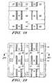
- FIG. 18includes an illustration of a top view of the workpiece of FIG. 12 after formation of doped regions within the substrate.
- FIGS. 19 and 20include illustrations of a top view and a cross-sectional view, respectively, of the workpiece of FIG. 18 after fabrication of an electronic device is substantially completed.
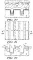
- FIGS. 21 and 22include illustrations of a top view and a cross-sectional view, respectively, of the workpiece of FIG. 13 after formation of doped regions within the substrate.
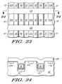
- FIGS. 23 and 24include illustrations of a top view and a cross-sectional view, respectively, of the workpiece of FIGS. 21 and 22 after fabrication of an electronic device is substantially completed.
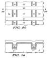
- FIGS. 25 and 26include illustrations of a top view and cross-sectional view of the workpiece of FIGS. 12 , respectively, except with trenches that are more widely spaced apart from each other.
- FIGS. 27 and 28include illustrations of a top view and a cross-sectional view of the workpiece of FIGS. 25 and 26 after fabrication of an electronic device is substantially completed.
- FIGS. 29includes an illustration of a cross-sectional view of the workpiece of FIG. 6 after formation of a conductive layer.
- FIG. 30includes an illustration of a cross-sectional view of the workpiece of FIG. 29 after formation of gate electrodes.
- FIGS. 31 through 42includes circuit schematic diagrams, cross-sectional views of exemplary physical embodiments of the circuit schematic diagrams, and operating voltage tables for memory cell along a row within an NVM array.
- An electronic devicecan include discontinuous storage elements that lie within a trench.
- the electronic devicecan include a substrate that includes a first trench.
- the trenchcan include a wall and a bottom and extends from a primary surface of the substrate.
- the electronic devicecan also include discontinuous storage elements, wherein a first portion of the discontinuous storage elements lie at least within the trench.
- the electronic devicecan further include a first gate electrode overlying the first portion of the discontinuous storage elements, wherein an upper surface of the first gate electrode lies below the primary surface of the substrate.
- the electronic devicecan also include a second gate electrode overlies the first gate electrode. In one embodiment, a second portion of the discontinuous storage elements that lie between the second gate electrode and the primary surface of the substrate.
- Embodiments described hereinalso include processes for forming the electronic device.
- the electronic devicecan include a memory array in which bit lines, gate lines, or any combination thereof can take advantage of the trench design and buried bit lines.
- a select gate linemay be electrically connected to a different number of rows or columns of memory cells as compared to a control gate line.
- a select gate linemay be electrically connected to one row or one column of memory cells, and the control gate line may be electrically connected to two rows or two columns of memory cells.
- a similar relationshipmay exist for bit lines.
- a select gate line and a control gate linemay be substantially perpendicular to each other.
- the select gate linemay be electrically connected to a different number of rows or columns of memory cells as compared to the control gate line.
- a select gate linemay be electrically connected to one row or one column of memory cells, and the control gate line may be electrically connected to two columns or two rows of memory cells.
- discontinuous storage elementsis spaced-apart objects capable of storing a charge.
- substantially all discontinuous storage elementsmay be initially formed and remain separate from one another.
- a substantially continuous layer of materialformed an later separated into discontinuous storage elements.
- substantially all discontinuous storage elementsmay be initially formed separate from one another, and later during the formation, some but not all of the discontinuous storage elements may coalesce.
- the term “primary surface”is intended to mean a surface of a substrate from which memory cells within a memory array are subsequently formed.
- the primary surfacemay be an original surface of a substrate before forming any electronic components or may be a surface from which trenches or other permanent structures within the memory array are formed.
- the memory arraymay be formed at least partly within an epitaxial layer overlying a base material, and electronic components within peripheral area (outside the memory array) may be formed from the base material.
- the primary surfacerefers to the upper surface of the epitaxial layer, and not the original surface of the base material.
- a non-volatile memory stackcan include layers used to form at least part of a non-volatile memory cell.
- a stackmay be part of a larger stack.
- a non-volatile memory stackcan include a charge storage stack that is used to store charge within a non-volatile memory cell.
- the terms “comprises,” “comprising,” “includes,” “including,” “has,” “having” or any other variation thereof,are intended to cover a non-exclusive inclusion.
- a process, method, article, or apparatus that comprises a list of elementsis not necessarily limited to only those elements but may include other elements not expressly listed or inherent to such process, method, article, or apparatus.
- “or”refers to an inclusive or and not to an exclusive or. For example, a condition A or B is satisfied by any one of the following: A is true (or present) and B is false (or not present), A is false (or not present) and B is true (or present), and both A and B are true (or present).
- FIG. 1includes a cross-sectional view of a portion of electronic device 10 , such as an integrated circuit.
- the integrated circuitcan be a standalone memory, a microcontroller, or other integrated circuit that includes a memory.
- electronic device 10can include non-volatile memory (“NVM”) array 18 , a portion of which is illustrated in FIG. 1 .
- NVMnon-volatile memory
- Substrate 12can include a monocrystalline semiconductor wafer, a semiconductor-on-insulator wafer, a flat panel display (e.g., a silicon layer over a glass plate), or other substrate conventionally used to form electronic devices.
- shallow trench field isolationmay be formed over portions of substrate 12 in peripheral areas, which are outside NVM array 18 .
- the doping concentration of substrate 12 along primary surface 13 within NVM array 18can be increased using a conventional doping operation to potentially reduce leakage current between subsequently-formed gate electrodes that may overlie portions of primary surface 13 .
- Protective layer 110can be formed over substrate 12 .
- Protective layer 110can include pad layer 14 , overlying substrate 12 and oxidation-resistant layer 16 , over pad layer 14 .
- Protective layer 110could have more or fewer layers than are illustrated.
- the upper most surface of substrate 12illustrated as contacting pad layer 14 , is primary surface 13 .
- Protective layer 110can remain over the peripheral areas until fabrication of NVM array 18 is substantially completed.
- pad layer 14includes oxide
- oxidation-resistant layer 16includes nitride.
- a patterned resist layer(not illustrated), which includes openings at locations within NVM array 18 where trenches are to be formed, is formed over substrate 12 by a conventional technique. Exposed portions of protective layer 110 can then be removed by a conventional technique to expose primary surface 13 . In one embodiment, trenches 22 and 23 , as illustrated in FIG. 2 , are formed prior to removal of the patterned resist layer. In another embodiment, the patterned resist layer is then removed, and trenches 22 and 23 can then be formed by a conventional technique. Trenches 22 and 23 are spaced apart from each other, extend from primary surface 13 , and include walls and bottoms.
- the depth of trenches 22 and 23can, at least in part, determine the channel length of one or more of the memory cells being formed adjacent to trenches 22 and 23 .
- the depths of trenches 22 and 23are in a range of approximately 50 to approximately 500 nm.
- trenches 22 and 23are formed using a timed anisotropic etch to produce substantially vertical walls.
- trenches 22 and 23have substantially uniform depths.
- Insulating layer 32is formed along the exposed surfaces of trenches 22 and 23 , as illustrated in FIG. 3 .
- Insulating layer 32may or may not be substantially conformal.
- insulating layer 32may include an oxide, a nitride, an oxynitride, or a combination thereof.
- insulating layer 32can be used as an implant screen.
- insulating layer 32is formed by thermally oxidizing the exposed portions of substrate 12 within trenches 22 and 23 . Thermal oxidation can be beneficial in removing defects, such as those induced by etching, help to round corners of trenches 22 and 23 , or a combination thereof.
- insulating layer 32can be deposited. A deposited insulating layer 32 would cover substantially all exposed surfaces of the workpiece.
- a dopantis introduced into portions of substrate 12 at the bottom of trenches 22 and 23 to form doped regions 52 and 53 , as illustrated in top and cross-sectional views, in FIGS. 4 and 5 , respectively.
- Doped region 52lies within substrate 12 and below trench 22
- doped region 53lies within substrate 12 and below trench 23 .
- Doped regions 52 and 53can be source/drain (“S/D”) regions and act as buried bit lines.
- the dopantmay be a p-type dopant (e.g., boron) or an n-type dopant (e.g., phosphorus or arsenic).
- the dopantcan be introduced using ion implantation.
- An optional thermal cyclecan be performed to activate the dopant.
- subsequent processingmay have one or more thermal cycles capable of activating the dopant.
- the doping concentration of doped regions 52 and 53is at least approximately 1E19 atoms/cm 3 .
- protective layer 110 within NVM array 18are removed by conventional techniques.
- Charge storage stack 68including dielectric layer 62 , discontinuous storage elements 64 , and dielectric layer 66 , can then be formed, as illustrated in FIG. 6 .
- insulating layer 32can be removed prior to formation of dielectric layer 62 over the exposed surface of trenches 22 and 23 , including the walls and bottoms of trenches 22 and 23 .
- insulating layer 32is used in place of or in conjunction with dielectric layer 62 .
- Dielectric layer 62may be thermally grown using an oxidizing or nitridizing ambient, or deposited using a conventional chemical vapor deposition technique, physical vapor deposition technique, atomic layer deposition technique, or a combination thereof.
- Dielectric layer 62can include one or more films of silicon dioxide, silicon nitride, silicon oxynitride, a high dielectric constant (“high-k”) material (e.g., dielectric constant greater than 8), or any combination thereof.
- the high-k materialcan include Hf a O b N c , Hf a Si b O c , Hf a Si b O c N d , Hf a Zr b O c N d , Hf a Zr b Si b O c N d , Hf a Zr b O c , Zr a Si b O c , Zr a Si b O c N d , ZrO 2 , other Hf-containing or Zr-containing dielectric material, a doped version of any of the foregoing (lanthanum doped, niobium doped, etc.), or any combination thereof.
- Dielectric layer 62has a thickness in a range of approximately 1 to approximately 10 nm. The thickness and material selection of dielectric layer 62 will substantially determine its electrical properties. In one embodiment the thickness and material are chosen such that dielectric layer 62 has a silicon dioxide equivalent thickness of less than 10 nm.
- Discontinuous storage elements 64are then formed over NVM array 18 .
- one portion of discontinuous storage elements 64lie at least within trench 22
- another portion of discontinuous storage elements 64lie at least within trench 23 .
- the individual discontinuous storage elements 64are substantially physically separated from each other.
- Discontinuous storage elements 64can include a material capable of storing a charge, such as silicon, a nitride, a metal-containing material, another suitable material capable of storing charge, or any combination thereof.
- discontinuous storage elements 64can include silicon nanocrystals or metal nanoclusters.
- a substantially continuous layer of amorphous siliconcan be formed over exposed surfaces of substrate 12 .
- Discontinuous storage elements 64may be undoped, doped during deposition, or doped after deposition. In one embodiment, discontinuous storage elements 64 can be formed from one or more materials whose properties are not significantly adversely affected during a thermal oxidation process. Such a material can include platinum, palladium, iridium, osmium, ruthenium, rhenium, indium-tin, indium-zinc, aluminum-tin, or any combination thereof. Each of such materials, other than platinum and palladium, may form a conductive metal oxide.
- each of discontinuous storage elements 64is no greater than approximately 10 nm in any dimension. In another embodiment, discontinuous storage elements 64 can be larger, however, discontinuous storage elements 64 are not formed so large as to form a continuous structure (i.e., all discontinuous storage elements 64 are not fused together).
- Dielectric layer 66is then formed over discontinuous storage elements 64 .
- Dielectric layer 66can include one or more dielectric films, any of which may be thermally grown or deposited.
- Dielectric layer 66can include any one or more materials or be formed using any of the embodiments as described with respect to dielectric 62 layer.
- Dielectric layer 66can have the same or different composition compared to dielectric 62 layer and may be formed using the same or different formation technique compared to dielectric layer 62 .
- Conductive layer 72is then formed overlying the workpiece, as illustrated in FIG. 7 .
- Conductive layer 72can include one or more semiconductor-containing or metal-containing films.
- conductive layer 72includes polysilicon or amorphous silicon deposited by a chemical vapor deposition process.
- conductive layer 72may include one or more other materials or may be deposited by another process.
- conductive layer 72is doped when deposited, and in another particular embodiment, is doped after it is deposited. The thickness of conductive layer 72 is sufficient to at least substantially fill in the trenches within NVM array 18 .
- the thickness of conductive layer 72is in a range of approximately 50 to approximately 500 nm, and in a finished device, remaining portions of conductive layer 72 have a dopant concentration of at least 1E19 atoms/cm 3 when conductive layer 72 includes polysilicon or amorphous silicon.
- Portions of conducting layer 72 overlying primary surface 13 and lying outside trenches 22 and 23can be removed, as illustrated in FIGS. 8 and 9 .
- FIG. 8 and other top viewssome dielectric or insulating layers are not illustrated to simplify understanding of positional relationships between features within NVM array 18 .
- Additional portions of conductive layer 72are removed such that the remaining material is recessed below primary surface 13 and contained within trenches 22 and 23 to form gate electrodes 92 and 93 , each of which has an upper surface that lies below primary surface 13 .
- Gate electrode 92overlies one portion of discontinuous storage elements 64 within trench 22
- gate electrode 93overlies another portion of discontinuous storage elements 64 within trench 23 .
- each of gate electrodes 92 and 93has a substantially rectangular shape, as seen from a cross-sectional view.
- conductive layer 72is undoped polysilicon, as initially deposited.
- Gate electrodes 92 and 93are then doped by conventional techniques such that in a finished device, gate electrodes 92 and 93 have a concentration of at least 1E19 atoms/cm 3 .
- a material capable of reacting with silicon to form a silicideand can include Ti, Ta, Co, W, Mo, Zr, Pt, other suitable material, or any combination thereof is formed on gate electrodes 92 and 93 and reacted to form a metal silicide.
- removal of a portion of conductive layer 72is accomplished by polishing with a conventional technique, followed by a timed etch. In another embodiment (not illustrated), the removal is accomplished by an etch process without polishing. In another embodiment the recess, which is the elevational difference between the primary surface 13 and the tops of the gate electrodes 92 and 93 , is between 20% and 80% of the depth of trenches 22 and 23 .
- the insulating layercan include one or more dielectric films, any of which may be thermally grown or deposited.
- the insulating layercan include any one or more materials or be formed using any of the embodiments as described with respect to dielectric 62 layer.
- the insulating layercan have the same or different composition compared to dielectric 62 layer and may be formed using the same or different formation technique compared to dielectric layer 62 .
- the thickness of intergate dielectric portions 104 and 105can affect the electrical fields within the channel regions of the memory cells. The electrical field is designed to provide the highest change in electrical field within the channel region for each memory cell to allow for source-side injection. In one embodiment, the thickness of intergate dielectric portions 104 and 105 is in a range of approximately 10 to approximately 30 nm.
- Conductive layer 112is formed over NVM array 18 , as illustrated in FIG. 11 .
- Conductive layer 112can include one or more semiconductor-containing or metal-containing films.
- conductive layer 112is doped polysilicon.
- conductive layer 112is formed from a metal containing material.
- the thickness of conductive layer 112is in a range of approximately 20 to approximately 300 nm.
- conductive layer 112has a dopant concentration of at least approximately 1E19 atoms/cm 3 when conductive layer 112 includes polysilicon or amorphous silicon.
- Conductive layer 112is patterned by etching using a conventional technique to form conductive lines 122 and 123 , which include gate electrodes, as illustrated in FIG. 12 .
- Conductive lines 122 and 123can lie at least partly within trench 22 , trench 23 , one or more other trenches (not illustrated) within NVM array 18 , or any combination thereof In one embodiment, the lengths of conductive lines 122 and 123 are substantially perpendicular to the lengths of trenches 22 and 23 within NVM array 18 .
- a material capable of reacting with silicon to form a silicidee.g., Ti, Ta, Co, W, Mo, Zr, Pt, other suitable material, or any combination thereof
- a material capable of reacting with silicon to form a silicideis formed on conductive line 122 and 123 and reacted to form a metal silicide.
- conductive lines 122 and 123can be used as word lines for NVM array 18 , with portions thereof acting as gate electrodes for plurality of bit cells.
- sidewall spacersmay be formed adjacent to conductive lines 122 and 123 .
- NVM array 18is substantially complete. Peripheral electrical connections (not illustrated) are made to access conductive portions of NVM array 18 .
- Protective layer 110 overlying the peripheral areas of substrate 12can be removed, and another protective layer (not illustrated) can be formed over NVM array 18 , which may protect NVM array 18 during component fabrication within the peripheral areas. Processing can be continued to form a substantially completed electronic device.
- One or more insulating layers, one or more conductive layers, and one or more encapsulating layersare formed using one or more conventional techniques.
- NVM array 18 layout and interconnect schememay be used.
- the process through formation of conductive layer 112 over all of NVM array 18can be performed using any embodiment as previously described.
- Conductive layer 112can be patterned and etched to form conductive lines 132 through 135 , as illustrated in FIG. 13 .
- the conductive lines 132 through 135can act as word lines in the NVM array 18 .
- the lengths of conductive lines 132 through 135are substantially parallel to the lengths of trenches 22 and 23 .
- portions of conductive lines 132 through 135can lie within the recesses of trenches 22 and 23 .
- the composition and method of formation of conductive lines 132 through 135may be any of those described with respect to formation of conductive lines 122 through 123 .
- Exposed portions of charge storage stack 68including discontinuous storage elements 64 , that overlie primary surface 13 can be removed using a conventional technique.
- an insulating layer(not illustrated) can be grown or deposited over primary surface 13 of substrate 12 and along exposed surfaces of conductive lines 132 through 135 .
- the insulating layercan help to protect sidewalls of conductive lines 132 through 135 and act as an implant screen during a subsequent doping operation to form source/drain regions along primary surface 13 and outside trenches 22 and 23 .
- sidewall spacers 136may be formed adjacent to conductive lines 132 through 135 .
- Patterned resist layer 146is formed over the workpiece to expose portions of conductive lines 132 through 135 and portions of the insulating layer (not illustrated in FIG. 15 ). In one embodiment, openings in patterned resist layer 146 substantially correspond to locations over which bit lines will subsequently be formed.
- a dopantis introduced into portions of substrate 12 to form doped regions 154 , as illustrated in FIG. 15 .
- the dopantmay be a p-type dopant (e.g., boron) or an n-type dopant (e.g., phosphorus or arsenic). In one embodiment, the dopant can be introduced using ion implantation. Patterned resist layer 146 is then removed by a conventional technique.
- the implanted dopantis activated by one or more subsequent thermal cycles, which may or may not serve a different primary purpose such as oxidation, deposition, annealing, drive or activation of a different implant dopant.
- each of doped regions 154has a dopant concentration of at least approximately 1E19 atoms/cm 3 .
- doped regions 154serve as S/D regions.
- NVM array 18is now substantially complete other than electrical connections. Remaining portions of protective layer 110 (not illustrated in FIG. 15 ) that overlie the peripheral areas of substrate 12 are removed, and another protective layer (not illustrated) can be formed over NVM array 18 which may protect NVM array 18 during component fabrication within the peripheral areas. Component fabrication within the peripheral areas can be performed using one or more conventional techniques. After the component fabrication within the peripheral areas is substantially completed, the protective layer overlying NVM array 18 can be removed.
- Interlevel dielectric layer 152is formed over the workpiece by a conventional technique. Interlevel dielectric layer 152 is patterned to form contact openings that extend to doped regions 154 and to other portions of NVM array 18 that are not illustrated in FIG. 15 . Interlevel dielectric layer 152 can include an insulating material, such as an oxide, a nitride, an oxynitride, or a combination thereof. In a specific embodiment, an anisotropic etch can be used to form contact openings.
- Conductive plugs 162 and conductive lines 164 and 165are then formed, as illustrated in FIGS. 16 and 17 .
- the lengths of conductive lines 164 and 165are substantially perpendicular to the lengths of conductive lines 132 through 135 , as illustrated in FIG. 16 .
- conductive lines 164 and 165are bit lines for NVM array 18
- conductive plugs 162are bit line contacts. Referring to FIG. 16 , portions of substrate 12 are illustrated lying between conductive lines 164 and 165 . Although not illustrated in FIG. 16 , doped regions 154 underlie conductive lines 164 and 165 between portions of substrate 12 .
- conductive plugs 162are formed prior to conductive lines 164 and 165 .
- a conductive layer(not illustrated) is formed over interlevel dielectric layer 152 and substantially fills contact openings therein. Portions of the conductive layer that lie outside the contact openings are removed to form conductive plugs 162 .
- a conventional chemical-mechanical polishing operationcan be performed, and in another embodiment, a conventional etching process can be performed.
- Another insulating layer(not illustrated) is then deposited and patterned to form trenches where conductive lines 164 and 165 will subsequently be formed. Other trenches can be formed at locations within NVM array 18 , outside NVM array 18 , or a combination thereof.
- another conductive layeris formed over interlevel dielectric layer 152 and substantially fills the trenches in the insulating layer. Portions of the conductive layer that lie outside the trenches within the insulating layer are removed to form conductive lines 164 and 165 .
- a conventional chemical-mechanical polishing operationcan be performed, and in another embodiment, a conventional etching process can be performed.
- the insulating layercan lie at substantially the same elevation between conductive lines 164 and 165 .
- conductive plugs 162 and conductive lines 164 and 165are formed concurrently using a conventional dual-inlaid process.
- Conductive plugs 162 and conductive lines 164 and 165can include the same or different conducting materials.
- Each of conductive plugs 162 and conductive lines 164 and 165can include doped silicon, tungsten, titanium, tantalum, titanium nitride, tantalum nitride, aluminum, copper, another suitable conductive material, or any combination thereof.
- conductive plugs 162include tungsten
- conductive lines 164 and 165include copper.
- An optional barrier layer, adhesion layer, or a combination thereofmay be formed before the corresponding conductive layers (e.g., tungsten for conductive plugs 162 and copper for conductive lines 164 and 165 ).
- An optional capping layere.g., a metal-containing nitride may be used to encapsulate copper within conductive lines 164 and 165 .
- additional insulating and conductive layerscan be formed and patterned to form one or more additional levels of interconnects.
- passivation layer 172is formed over substrate 12 , including NVM array 18 and peripheral areas.
- Passivation layer 172can include one or more insulating film, such as an oxide, a nitride, an oxynitride, or a combination thereof.
- yet another NVM array 18 layout and interconnect schememay be used.
- the process through formation of conductive lines 122 and 123can be performed using any embodiment as previously described with respect to FIGS. 1 to 12 .
- remaining portions (not illustrated) of protective layer 110 that overlie the peripheral areas of substrate 12are removed, and another protective layer (not illustrated) can be formed over NVM array 18 which may protect NVM array 18 during component fabrication within the peripheral areas.
- Component fabrication within the peripheral areascan be performed using one or more conventional techniques.
- the protective layer overlying NVM array 18can be removed.
- the exposed portions of charge storage stack 68can also be removed.
- the remainder of processing for the peripheral areas and NVM array 18can occur substantially simultaneously.
- a dopantis introduced into substrate 12 to form doped region 182 at locations between conductive lines 122 and 123 and outside and adjacent to trenches 22 and 23 , as illustrated in FIG. 18 .
- Doped region 182can include any one or more materials or be formed using any of the embodiments as described with respect to doped region 154 .
- Doped region 182can have the same or different composition compared to doped region 154 and may be formed using the same or different formation technique compared to doped region 154 .
- spacersmay be formed adjacent to conductive lines 122 and 123 before, after, or between individual actions used in forming doped region 182 .
- the optional sidewall spacerscan be formed as previously described regarding other embodiments.
- doped region 182can serve as S/D regions in the finished device.
- doped region 182has a dopant concentration of at least approximately 1E19 atoms/cm 3 .
- a metal silicidecan be formed from portions of conductive lines 122 and 123 , doped region 182 , or any combination thereof, using a conventional technique.
- Interlevel dielectric layer 152is then formed and patterned to form contact openings, as illustrated in FIGS. 19 and 20 , using any of the embodiments as previously described with respect to formation and patterning of interlevel dielectric layer 152 .
- the locations of the contact openingsare changed as compared to a prior embodiment in that contact openings extend to doped regions 182 .
- interlevel dielectric layer 152can be formed as previously described.
- Conductive plugs 192are then formed using any embodiment as previously described for conductive plugs 162 .
- the locations of conductive plugs 192are different from those illustrated for conductive plugs 162 .
- insulating layer 193is then deposited over interlevel dielectric layer 152 and conductive plugs 192 and patterned to form trenches where conductive lines 194 through 196 will subsequently be formed. Other trenches can be formed at locations within NVM array 18 , outside NVM array 18 , or a combination thereof.
- Conductive lines 194 through 196are then formed using any embodiment as previously described for conductive lines 164 and 165 . Conductive lines 194 through 196 can serve as bit lines within NVM array 18 .
- the locations of conductive plugs 192 and conductive lines 194 through 196are different from those illustrated for conductive plugs 162 and conductive lines 164 and 165 , respectively.
- the orientation of conductive lines 194 through 196is different from the orientation of conductive lines 164 and 165 .
- the lengths of conductive lines 194 through 196are substantially perpendicular to the lengths of conductive lines 132 and 133 , as illustrated in FIG. 19 .
- additional insulating and conductive layerscan be formed and patterned to form additional levels of interconnects.
- passivation layer 172is formed over substrate 12 , including NVM array 18 and peripheral areas.
- Passivation layer 172can include one or more insulating film, such as an oxide, a nitride, an oxynitride, or a combination thereof.
- NVM array 18 layout and interconnect schememay be used.
- the layout and interconnect schemeis similar to an embodiment as illustrated in FIGS. 1 through 13 and 18 through 20 except that a virtual ground array architecture is used, rather than conductive lines 194 through 196 .
- the layout and organizationwill become more apparent after reading the description below with respect to FIGS. 21 to 25 .
- openings 210are formed within the protective layer 110 , and doped regions 214 , 215 , and 216 are formed along primary substrate 13 of substrate 12 outside trenches 22 and 23 , as illustrated in FIGS. 21 and 22 , which are similar to FIGS. 4 and 5 , respectively.
- Openings 210 and doped regions 214 , 215 , and 216can be formed using one or more conventional techniques. Openings 210 can be formed before or after forming trenches 22 and 23 . For example, all openings within protective layer 110 may be formed at substantially simultaneously.
- a mask(not illustrated) can be formed over opening 210 to substantially prevent forming a trench below openings 210 . The mask can be removed after forming trenches 22 and 23 .
- a different mask(not illustrated) may be formed over openings 210 after trenches 22 and 23 have been formed, and the different mask can be removed after forming openings 210 .
- Insulating layer 32can be formed along the bottoms of openings 210 in a manner similar to the embodiment described with respect to FIG. 3 .
- Doped regions 214 , 215 , and 216can be formed using any one or more of the embodiments as described with respect to doped regions 52 and 53 .
- the dopant species, concentration, and profile and formation of doped regions 214 , 215 , and 216may be the same or different as compared to doped regions 52 and 53 .
- doped regions 214 , 215 , and 216can be formed substantially simultaneously with doped regions 52 and 53 .
- Each of doped regions 52 , 53 , 214 , 215 , and 216have lengths that are substantially parallel to one another and can act as buried bit lines.
- Doped regions 52 and 53lie at elevations deeper within substrate 12 , as compared to doped regions 214 , 215 , and 216 .
- openings 210are not formed. Instead, after forming trenches 22 and 23 , remaining portions of protective layer 110 within NVM array 18 are removed before forming insulating layer 32 . Doped regions 214 , 215 , and 216 can be formed when doped regions 52 and 53 are formed. Doped regions 214 , 215 , and 216 can extend to walls of trenches 22 and 23 .
- FIGS. 23 and 24include illustrations of a portion of NVM array 18 are formation of the NVM array is substantially completed. As compared to the conductive lines 194 through 196 in FIGS. 19 and 20 , doped regions 214 through 216 can be used in place of conductive lines 194 to 196 .
- peripheral electrical connectionsare made to access conductive portions of NVM array 18 .
- Protective layer 110 overlying the peripheral areas of substrate 12can be removed, and another protective layer (not illustrated) can be formed over NVM array 18 , which may protect NVM array 18 during component fabrication within the peripheral areas. Processing can be continued to form a substantially completed electronic device.
- One or more insulating layers, one or more conductive layers, and one or more encapsulating layersare formed using one or more conventional techniques.
- NVM array 18 layout and interconnect schememay be used.
- the layout and interconnect schemeis similar to an embodiment as illustrated in FIGS. 1 to 12 and 18 to 20 except that a plurality of bit lines lie between trenches 22 and 23 , and electrical connections are made between the bit lines and only some of the doped regions underlie the bit lines.
- the layout and organizationwill become more apparent after reading the description below with respect to FIGS. 25 to 28 .
- the process through formation of conductive lines 122 and 123can be performed using any embodiment as previously described with respect to FIGS. 1 to 12 .
- the space between trenches 22 and 23may be increased to allow for the proper formation of bit lines and contacts consistent with the design rules, as illustrated in FIGS. 25 and 26 .
- remaining portions (not illustrated) of protective layer 110 that overlie the peripheral areas of substrate 12are removed, and another protective layer (not illustrated) can be formed over NVM array 18 which may protect NVM array 18 during component fabrication within the peripheral areas.
- Component fabrication within the peripheral areascan be performed using one or more conventional techniques. After the component fabrication within the peripheral areas is substantially completed, the protective layer overlying NVM array 18 can be removed.
- Formation of conductive lines 122 and 123 and doped regions 212can be performed using any one of the embodiments as described with respect to conductive lines 122 and 123 and doped regions 182 , as illustrated in FIG. 18 .
- An interlevel dielectric layer 152is then formed and patterned to form contact openings, as illustrated in FIGS. 27 and 28 , using any of the embodiments as previously described with respect to formation and patterning of interlevel dielectric layer 152 . The locations of the contact openings are changed in that contact openings extend to doped regions 212 .
- conductive plugs 232 and conductive lines 234 through 237are then formed using any embodiment as previously described for conductive plugs 192 and conductive lines 194 through 196 .
- Conductive lines 234 through 237can serve as bit lines within NVM array 18 .
- the locations of conductive plugs 232 and conductive lines 234 through 237are different from those illustrated for conductive plugs 192 and conductive lines 194 through 196 , respectively.
- the orientation of conductive lines 234 through 237is substantially the same as the orientation of conductive lines 194 through 196 .
- the lengths of conductive lines 234 and 234are substantially perpendicular to the lengths of conductive lines 122 and 123 , as illustrated in FIG. 27 .
- each of conductive lines 234 through 237has electrical connections via conductive plugs 232 to only some of the underlying doped regions 222 .
- the electrical connections to underlying doped regions 222are alternated between conductive lines 235 and 236 .
- conductive line 235is electrically connected to the middle row of doped regions 222
- a conductive line 236is electrically connected to the top and bottom rows of doped regions 222 .
- additional insulating and conductive layerscan be formed and patterned to form additional levels of interconnects.
- passivation layer 172is formed over substrate 12 , including NVM array 18 and peripheral areas.
- Passivation layer 172can include one or more insulating film, such as an oxide, a nitride, an oxynitride, or a combination thereof.
- the gate electrodes within trenches 22 and 23can have a shape similar to a sidewall spacer.
- the processmay start with the workpiece as illustrated in FIG. 6 .
- Conductive layer 252can be deposited as illustrated in FIG. 29 .
- conductive layer 252is a relatively thinner, substantially conformal layer.
- Conductive layer 252can be formed using any one or more embodiments as described with respect to conductive layer 72 .
- the thickness of conductive layer 252is insufficient to fill in trench structure 22 and 23 within NVM array 18 . In one embodiment, the thickness of conductive layer 252 is in a range of approximately 10 nm to approximately 100 nm.
- gate electrodes 262 and 263 illustrated in FIG. 30An anisotropic etch of conductive layer 252 can then form gate electrodes 262 and 263 illustrated in FIG. 30 .
- gate electrodes 262 and 263can have substantially sidewall spacer shapes within trenches 22 and 23 .
- gate electrodes 262 and 263are annular, in that each of gate electrodes 262 and 263 lies along the perimeter of trenches 22 and 23 .
- the spaced-apart left and right portions with facing curved surfaces for each of gate electrodes 262 and 263 within each of trenches 22 and 23are connected to each other.
- the processing of NVM array 18can then be completed as previously described for other embodiments.
- an additional isotropic etch portionmay be used to reduce the likelihood of forming an unintended electrical connection or leakage path between subsequently-formed conductive lines 122 and 123 .
- doped regions that are at least part of source/drain regions for the memory cells within NVM array 18have an opposite conductivity type as compared to substrate 12 .
- the portion of substrate 12 as illustrated in the figuresmay or may not lie within one or more well regions. Such well region(s) may be different from one or more other well regions within peripheral areas (outside NVM array 18 ).
- Other dopingcan be performed that may affect breakdown voltages, resistivity, threshold voltage, hot carrier generation, one or more other electrical characteristics, or any combination thereof. Skilled artisans will be able to form electronic devices having doping characteristics that meet their needs or desires.
- NVM array 18can include memory cells using any of the layouts as previously described. Circuit schematics and cross references to physical embodiments are described to illustrate better how memory cells within NVM array 18 can be electrically configured and programmed.
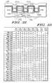
- FIG. 31includes a circuit schematic for an embodiment as described with respect to the embodiment as illustrated in FIG. 32 .
- Memory cells 2711 , 2712 , 2721 , and 2722are oriented within NVM array 18 , as illustrated in FIG. 31 .
- BLrefers to a bit line
- GLrefers to a gate line.
- a GLcan be a control gate line or a select gate line, depending on the biasing conditions.
- BL 1 2762is electrically connected to a S/D region of memory cell 2711 and a S/D region of memory cell 2721 .
- BL 2 2764is electrically connected to the other S/D regions of memory cells 2711 and 2721 and to a S/D region of memory cell 2712 and a S/D region of memory cell 2722 .
- BL 3 2766is electrically connected to the other S/D regions of memory cells 2712 and 2722 .
- GL 1 2742is electrically connected to a gate electrode of memory cell 2711 and a gate electrode of memory cell 2721 .
- GL 2 2744is electrically connected to gate electrodes of memory cells 2711 and 2712 .
- GL 3 27846is electrically connected to other gate electrodes of memory cells 2711 and 2721 and to a gate electrode of memory cell 2712 and a gate electrode of memory cell 2722 .
- GL 4 2748is electrically connected to gate electrodes of memory cells 2712 and 2722 .
- GL 5 2705is electrically connected to other gate electrodes of memory cells 2721 and 2722 .
- FIG. 32illustrates a physical embodiment of a portion of NVM array 18 corresponding to the row that includes memory cells 2711 and 2712 .
- FIG. 32is a cross-sectional illustration of the workpiece of FIG. 12 labeled with the same reference numbers those used in the circuit schematics in FIG. 32 .
- Memory cell 2711includes charge storage regions 27111 to 27114
- memory cell 2712includes charge storage region 27121 to 27124
- Memory cells 2721 and 2722include similar charge storage regions, but such charge storage regions are not specifically identified in FIG. 31 .
- FIG. 33includes a table that has some of the operating voltages for memory cells, as illustrated in FIG. 31 .
- “Pgm”means program.
- References to charge storage regions 27111 , 27112 27113 , 27114 , 27115 , and 27116refer to memory cell 2711 , and more particularly to programming or reading discontinuous storage elements under gate electrodes of memory cell 2711 . While many voltages are given in the table in FIG. 33 and other tables within this specification, other voltages may be used. The relative values and ratios between the voltages, rather than their absolute values are more relevant, as the absolute values of voltages change with changes in physical parameters.
- All memory cells, as illustrated in FIG. 31can be erased by creating a potential difference in a range of about 12 to 16 volts between substrate 12 (or well region therein) and the gate electrodes of the memory cells.
- erasingcan be performed by placing substrate 12 (or well region therein) to approximately +7 volts, placing the gate lines to ⁇ 7 volts and allowing the bit lines to electrically float.
- erasingcan be performed by placing substrate 12 (or well region therein) to approximately ⁇ 7 volts, placing the gate lines to +7 volts and allowing the bit lines to electrically float.
- the voltages used for substrate 12 and the gate linedo not need to be symmetric with respect to 0 volts. For example, a combination of +5 volts and ⁇ 9 volts can be used. After reading this specification, skilled artisans will be able to determine a set of voltages to be used for erasing that meets their needs or desires.
- FIG. 34includes a circuit schematic for an embodiment as described with respect to the embodiment as illustrated in FIG. 35 .
- Memory cells 3011 , 3012 , 3013 , 3014 , 3021 , 3022 , 3023 , and 3024are oriented within NVM array 18 , as illustrated in FIG. 34 .
- BL 1 3062is electrically connected to a S/D region of memory cells 3011 , 3012 , 3013 , and 3014 .
- BL 2 3064is electrically connected to a S/D region of memory cells 3021 , 3022 , 3023 , and 3024 .
- BL 3 3066is electrically connected to the other S/D regions of memory cells 3011 , 3012 , 3021 , and 3022 .
- BL 4 3068is electrically connected to the other S/D regions of memory cells 3013 , 3014 , 3023 , and 3024 .
- GL 1 3042is electrically connected to select gate electrodes of memory cells 3011 and 3021 .
- GL 2 3044is electrically connected to control gate electrodes of memory cell 3011 , 3012 , 3021 , and 3022 .
- GL 3 3046is electrically connected to select gate electrodes of memory cells 3012 and 3022 .
- GL 4 3048is electrically connected to select gate electrodes of memory cells 3013 and 3023 .
- GL 5 3050is electrically connected to control gate electrodes of memory cells 3013 , 3014 , 3023 , and 3024 .
- GL 6 3052is electrically connected to select gate electrodes of memory cells 3014 and 3024 .
- FIG. 35illustrates a physical embodiment of a portion of NVM array 18 corresponding to the row that includes memory cells 3011 , 3012 , 3013 , and 3014 .
- FIG. 35is substantially the same as FIG. 17 except that reference numbers as used in the circuit schematics are used in FIG. 35 .
- Memory cell 3011includes charge storage regions 30111 to 30114
- memory cell 3012includes charge storage region 30121 to 30124
- memory cell 3013includes charge storage region 30131 to 30134
- memory cell 3014includes charge storage region 30141 to 30144 .
- Memory cells 3021 through 3024include similar charge storage regions, but such charge storage regions are not specifically identified in FIG. 34 .
- FIG. 36includes a table that has some of the operating voltages for memory cells, as illustrated in FIG. 34 .
- All memory cells, as illustrated in FIG. 34can be erased by creating a potential difference in a range of about 12 to 16 volts between substrate 12 (or well region therein) and the gate electrodes of the memory cells.
- erasingcan be performed by placing substrate 12 (or well region therein) to approximately +7 volts, placing the gate lines to ⁇ 7 volts and allowing the bit lines to electrically float.
- erasingcan be performed by placing substrate 12 (or well region therein) to approximately ⁇ 7 volts, placing the gate lines to +7 volts and allowing the bit lines to electrically float.
- the voltages used for substrate 12 and the gate linedo not need to be symmetric with respect to 0 volts. For example, a combination of +5 volts and ⁇ 9 volts can be used. After reading this specification, skilled artisans will be able to determine a set of voltages to be used for erasing that meets their needs or desires.
- FIG. 37includes a circuit schematic for an embodiment as described with respect to the embodiment as illustrated in FIG. 38 .
- Memory cells 3311 , 3312 , 3313 , 3314 , 3321 , 3322 , 3323 , and 3324are oriented within NVM array 18 , as illustrated in FIG. 37 .
- BL 1 3362is electrically connected to a S/D region of memory cell 3311 and a S/D region of memory cell 3321 .
- BL 2 3364is electrically connected to the other S/D regions of memory cells 3311 and 3321 and to S/D regions of memory cell 3312 and 3322 .
- BL 3 3366is electrically connected to the other S/D regions of memory cell 3312 and 3322 and to S/D regions of memory cell 3313 and 3323 .
- BL 4 3368is electrically connected to the other S/D regions of memory cell 3313 and 3323 and to S/D regions of memory cell 3314 and 3324 .
- BL 5 3369is electrically connected to the other S/D regions of memory cell 3314 and 3324 .
- GL 1 3342is electrically connected to select gate electrodes of memory cell 3311 , 3312 , 3313 , and 3314 .
- GL 2 3344is electrically connected to control gate electrodes of memory cell 3311 , 3312 , 3321 and 3322 .
- GL 3 3346is electrically connected to control gate electrodes of memory cell 3313 , 3314 , 3323 and 3324 .
- GL 4 3348is electrically connected to select gate electrodes of memory cell 3321 , 3322 , 3323 , and 3324 .
- FIG. 38illustrates a physical embodiment of a portion of NVM array 18 corresponding to the row that includes memory cells 3311 , 3312 , 3313 , and 3314 .
- FIG. 38is substantially the same as an embodiment of FIG. 20 except that reference numbers as used in the circuit schematics are used in FIG. 38 .
- Memory cell 3311includes charge storage regions 33111 to 33114
- memory cell 3312includes charge storage region 33121 to 33124
- memory cell 3313includes charge storage region 33131 to 33134
- memory cell 3314includes charge storage region 33141 to 33144 .
- charge storage regions 33111 , 33124 , 33131 , and 33144are not illustrated in FIG. 38 , because those charge storage regions are offset from the plane as illustrated in the cross-sectional view of FIG. 38 .
- Memory cells 3321 through 3324include similar charge storage regions, but such charge storage regions are not specifically identified in FIG. 37 .
- FIG. 39includes a table that has some of the operating voltages for memory cells, as illustrated in FIG. 37 .
- All memory cells, as illustrated in FIG. 37can be erased by creating a potential difference in a range of about 12 to 16 volts between substrate 12 (or well region therein) and the gate electrodes of the memory cells.
- erasingcan be performed by placing substrate 12 (or well region therein) to approximately +7 volts, placing the gate lines to ⁇ 7 volts and allowing the bit lines to electrically float.
- erasingcan be performed by placing substrate 12 (or well region therein) to approximately ⁇ 7 volts, placing the gate lines to +7 volts and allowing the bit lines to electrically float.
- the voltages used for substrate 12 and the gate linedo not need to be symmetric with respect to 0 volts. For example, a combination of +5 volts and ⁇ 9 volts can be used. After reading this specification, skilled artisans will be able to determine a set of voltages to be used for erasing that meets their needs or desires.
- FIGS. 21 through 24can be represented by the circuit schematic as illustrated in FIG. 37 and can be operated using the voltages as listed in FIG. 39 .
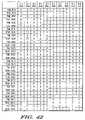
- FIG. 40includes a circuit schematic for an embodiment as described with respect to the embodiment as illustrated in FIG. 41 .
- Memory cells 3611 , 3612 , 3613 , 3614 , 3621 , 3622 , 3623 , and 3624are oriented within NVM array 18 , as illustrated in FIG. 40 .
- BL 1 3662is electrically connected to a S/D region of memory cell 3611 and a S/D region of memory cell 3621 .
- BL 2 3664is electrically connected to the other S/D regions of memory cell 3611 and 3621 and to S/D regions of memory cells 3612 and 3622 .
- BL 3 3666is electrically connected to the other S/D regions of memory cells 3612 and 3622 .
- BL 4 3668is electrically connected to S/D regions of memory cells 3613 and 3623 .
- BL 5 3670is electrically connected to the other S/D regions of memory cells 3613 and 3623 , and S/D regions of memory cells 3614 and 3624 .
- BL 6 3672is electrically connected to the other S/D regions of memory cells 3614 and 3624 .
- GL 1 3642is electrically connected to select gate electrodes of memory cell 3611 , 3612 , 3613 , and 3614 .
- GL 2 3644is electrically connected to control gate electrodes of memory cell 3611 , 3612 , 3621 , and 3622 .
- GL 3 3646is electrically connected to control gate electrodes of memory cell 3613 , 3614 , 3623 , and 3624 .
- GL 4 3648is electrically connected to select gate electrodes of memory cell 3621 , 3622 , 3623 , and 3624 .
- FIG. 41illustrates a physical embodiment of a portion of NVM array 18 corresponding to the row that includes memory cells 3611 , 3612 , 3613 , and 3614 .
- FIG. 41is substantially the same as FIG. 28 except that reference numbers as used in the circuit schematics are used in FIG. 41 .
- Memory cell 3611includes charge storage regions 36111 to 36114
- memory cell 3612includes charge storage region 36121 to 36124
- memory cell 3613includes charge storage region 36131 to 36134
- memory cell 3614includes charge storage region 36141 to 36144 .
- charge storage regions 36111 , 36124 , 36131 , and 36144are not illustrated in FIG. 41 , because those charge storage regions are offset from the plane as illustrated in the cross-sectional view of FIG. 41 .
- Memory cells 3621 through 3624include similar charge storage regions, but such charge storage regions are not specifically identified in FIG. 40 .
- FIG. 42includes a table that has some of the operating voltages for memory cells, as illustrated in FIG. 40 .
- All memory cells, as illustrated in FIG. 40can be erased by creating a potential difference in a range of about 12 to 16 volts between substrate 12 (or well region therein) and the gate electrodes of the memory cells.
- erasingcan be performed by placing substrate 12 (or well region therein) to approximately +7 volts, placing the gate lines to ⁇ 7 volts and allowing the bit lines to electrically float.
- erasingcan be performed by placing substrate 12 (or well region therein) to approximately ⁇ 7 volts, placing the gate lines to +7 volts and allowing the bit lines to electrically float.
- the voltages used for substrate 12 and the gate linedo not need to be symmetric with respect to 0 volts. For example, a combination of +5 volts and ⁇ 9 volts can be used. After reading this specification, skilled artisans will be able to determine a set of voltages to be used for erasing that meets their needs or desires.
- NVM array 18its memory cells, bit lines, and gate lines. After reading this specification, skilled artisans will appreciate that the row and column orientations can be reversed. Electrically connections between memory cells and their associated bit lines, gate lines, or any combination thereof along one or more rows can be changed to one or more columns. Similarly, electrically connections between memory cells and their associated bit lines, gate lines, or any combination thereof along one or more columns can be changed to one or more rows.
- Embodiments as described hereinare useful in forming NMV arrays or a portion thereof.
- the use of discontinuous storage elements within a trench in the substrateallows smaller memory cells to be formed and increase memory density.
- the discontinuous storage elementscan also allow more bits to be stored within a memory cell as opposed to a conventional floating gate structure.
- portions of the discontinuous storage elementslie between all of the gate electrodes and the substrate.
- the portions of the discontinuous storage elementslie between all of the gate electrodes and the substrate at substantially all locations where gate electrodes overlie the substrate.
- the portions of discontinuous storage elementscan allow up to six bits of data to be stored per memory cell.
- the fabrication of the NVM arraycan be implemented using existing materials and equipment. Therefore, process integration would not require developing new processes for new equipment or having to address materials incompatibility issues.
- the memory cellscan be formed such that select gate lines are formed, such that they are at least partly recessed within the trenches.
- Source-side injectioncan be used to program some of the charge storage regions of memory cells.
- the thickness of the intergate dielectric portions 114 and 115 and programming voltagescan be selected to allow a relatively larger electrical field to be generated near the intergate dielectric portions 114 and 115 as compared to near the S/D regions that are electrically connected to the bit lines.
- the source-side injectionallows programming times similar to conventional hot-electron injection and has a higher electron efficiency compared to conventional hot-electron injection.
- an electronic devicecan include a substrate, including a first trench that includes a wall and a bottom and extends from a primary surface of the substrate.
- the electronic devicecan also include discontinuous storage elements, wherein a first portion of discontinuous storage elements lies within the first trench.
- the electronic devicecan also include a first gate electrode having an upper surface that lies below the primary surface of the substrate, wherein at least a part of the first portion of the discontinuous storage elements lies along the wall of the first trench at an elevation between the upper surface of the first gate electrode and the primary surface, and a second gate electrode overlying the first gate electrode and the primary surface of the substrate.
- the electronic devicefurther includes a third gate electrode.
- the substratecan further include a second trench that is spaced apart from the first trench, wherein the second trench includes a wall and a bottom and extends from that primary surface of the substrate.
- the electronic devicecan further include a second portion of the discontinuous storage elements that lies at least within the second trench.
- the third gate electrodehas an upper surface that lies below the primary surface of the substrate, wherein at least a part of the second portion of the discontinuous storage elements lies along the wall of the second trench at an elevation between the upper surface of the third gate electrode and the primary surface.
- the electronic devicecan further include a first doped region lying within the substrate below the first trench, and a second doped region lying within the substrate below the second trench.
- the electronic devicefurther includes a third doped region lying along the primary surface of the substrate between the first and second trenches.
- the third doped regionextends to the walls of the first and second trenches.
- the third doped regionis spaced apart from the walls of the first and second trenches.
- a first charge storage regionincludes a first discontinuous storage element within the first portion of the discontinuous storage elements, wherein the first discontinuous storage element lies closer to the upper surface of the first gate electrode than the first doped region.
- a second charge storage regionincludes a second discontinuous storage element within the first portion of the discontinuous storage elements, wherein the second discontinuous storage element lies closer to the first doped region than the upper surface of the first gate electrode, and wherein the second charge storage region is spaced apart from the first charge storage region.
- a third charge storage regionincludes a third discontinuous storage element within the second portion of the discontinuous storage elements, wherein the third discontinuous storage element lies closer to the upper surface of the third gate electrode than the second doped region.
- a fourth charge storage regionincludes a fourth discontinuous storage element within the second portion of the discontinuous storage elements, wherein the fourth discontinuous storage element lies closer to the second doped region than the upper surface of the third gate electrode, and wherein the fourth charge storage region is spaced apart from the third charge storage region.
- the second gate electrodeoverlies the first gate electrode, the third gate electrode, and a portion the substrate between the first and second trenches.
- the electronic devicefurther includes a fourth gate electrode spaced apart from the third gate electrode, wherein the second gate electrode overlies the first gate electrode and a first portion of the substrate between the first and second trenches, and the fourth gate electrode overlies the third gate electrode and a second portion of the substrate between the first and second trenches.
- the electronicfurther includes an array, wherein within the array, the discontinuous storage elements overlie substantially all of the primary surface and along substantially all of the wall of the first trench.
- the discontinuous storage elementsinclude silicon nanocrystals or metal nanoclusters.
- the first gate electrodehas a substantially rectangular shape.
- the first gate electrodeincludes portions, and the portions of the first gate electrode include curved outer surfaces that face each other.
- an electronic devicecan include a substrate including a first trench and a second trench that are spaced apart from each other, wherein each of the first and second trenches includes a wall and a bottom and extends from a primary surface of the substrate.
- the substratecan also include a first doped region lying within the substrate along the bottom of the first trench, a second doped region lying within the substrate along the bottom of the second trench, and a first dielectric layer lying along the walls and bottoms of the first and second trenches.
- the electronic devicecan also include discontinuous storage elements, wherein a first portion of the discontinuous storage elements lie at least within the first trench, a second portion of the discontinuous storage elements lie at least within the second trench, and a third portion of the discontinuous storage elements overlie the primary surface of the substrate.
- the third portion of the discontinuous storage elementscan be contiguous with each of the first and second portions of the discontinuous storage elements.
- the electronic devicecan also include a second dielectric layer adjacent to the discontinuous storage elements within the first and second trenches.
- the electronic devicecan further include a first gate electrode lying within the first trench and having an upper surface that lies below the primary surface of the substrate, wherein at least a part of the first portion of the discontinuous storage elements lies along the wall of the first trench at an elevation between the upper surface of the first gate electrode and the primary surface.
- the electronic devicecan also include a second gate electrode lying within the second trench and having an upper surface that lies below the primary surface of the substrate, wherein at least a part of the second portion of the discontinuous storage elements lies along the wall of the second trench at an elevation between the upper surface of the second gate electrode and the primary surface.
- the electronic devicecan still further include a third dielectric layer including a first portion overlying the first gate electrode within the first trench and a second portion overlying the second gate electrode within the second trench.
- the electronic devicecan also include a third gate electrode overlying at least one of the first gate electrode or the second gate electrode, wherein the third gate electrode lies at least partly within the first trench and the second trench.
- an electronic devicecan include a first set of memory cells oriented substantially along a first direction, and a second set of memory cells oriented substantially along the first direction.
- the electronic devicecan also include a first conductive line electrically connected to the first set of memory cells, wherein the first conductive line is of a type including a gate line or a bit line.
- the electronic devicecan also include a second conductive line electrically connected to the second set of memory cells, wherein the second conductive line is of a same type as the first conductive line, and when compared to the first conductive line, the second conductive line is electrically connected to more sets of memory cells that lie along the first direction.
- each memory cell within the first and second sets of memory cellsincludes a nonvolatile memory cell that includes a first gate electrode and a second gate electrode.
- a discontinuous storage elementlies between a channel region and the first gate electrode, and another discontinuous storage element lies between the channel region and the second gate electrode.
- the electronic devicefurther includes a third set of memory cells oriented substantially along the first direction, wherein the first, second, and third sets of memory cells lie within different rows or different columns as compared to one another.
- Each memory cell within the third set of memory cellsincludes a nonvolatile memory cell that includes a first gate electrode and a second gate electrode.
- a discontinuous storage elementlies between a channel region and the first gate electrode, and another discontinuous storage element lies between the channel region and the second gate electrode.
- the first conductive lineis a first gate line that is electrically connected to the first gate electrodes of the first set of memory cells, and the second conductive line is a second gate line that is electrically connected to the second gate electrodes of the second and third sets of memory cells.
- the electronic devicefurther includes a third set of memory cells oriented substantially along the first direction, wherein the first, second, and third sets of memory cells lie within different rows or different columns as compared to one another.
- the first conductive lineis a first bit line
- the second conductive lineis a second bit line electrically connected to the second and third sets of memory cells.
- the first directionis associated with a row or a column.
- a process for forming an electronic devicecan include forming a first trench within a substrate, wherein the first trench includes a wall and a bottom and extends from a primary surface of the substrate.
- the processalso can include forming discontinuous storage elements over the primary surface and within the first trench, wherein a first portion of the discontinuous storage elements lie within the first trench.
- the processcan further include forming a first gate electrode within the first trench after forming the discontinuous storage elements, wherein the first gate electrode has an upper surface that lies below the primary surface of the substrate, and at least part of the first portion of the discontinuous storage elements lies between the first gate electrode and the wall of the first trench.
- the processcan still further include forming a second gate electrode that overlies the first gate electrode and the primary surface of the substrate, wherein after forming the second gate electrode, at least a part of the first portion of the discontinuous storage elements lies along the wall of the first trench at an elevation between an upper surface of the first gate electrode and the primary surface of the substrate.
- forming the second gate electrodeincludes forming the second gate electrode, such that at least a portion of the second gate electrode extends at least partly into the first trench.
- the processfurther includes forming a third gate electrode within a second trench.
- Forming the first trenchfurther includes forming a second trench that is spaced apart from the first trench, wherein the second trench, includes a wall and a bottom and extends from a primary surface of the substrate.
- Forming the discontinuous storage elementsfurther includes forming the discontinuous storage elements within the second trench, wherein a second portion of the discontinuous storage elements lie within the second trench.
- Forming the third gate electrodeincludes forming the third gate electrode, such that the third gate electrode has an upper surface that lies below the primary surface of the substrate, and at least a part of the second portion of the discontinuous storage elements lies between the third gate electrode and the wall of the second trench. After forming the second gate electrode, at least a part of the second portion of the discontinuous storage elements lies along the wall of the second trench at an elevation between the upper surface of the third gate electrode and the primary surface of the substrate.
- the processfurther includes forming a first doped region and a second doped region along the bottoms of the first and second trenches, respectively.
- the processfurther includes forming a third doped region lying along the primary surface of the substrate between the first and second trenches.
- forming the third doped regionis performed before forming the second gate electrode.
- forming the third doped regionis performed after forming the second gate electrode.
- a first charge storage regionafter forming the second gate electrode, includes a first discontinuous storage element, wherein the first discontinuous storage element lies closer to the upper surface of the first gate electrode than the first doped region.
- a second charge storage regionincludes a second discontinuous storage element within the first portion of the discontinuous storage elements, wherein the second discontinuous storage element lies closer to the first doped region than the upper surface of the first gate electrode, and wherein the second charge storage region is spaced apart from the first charge storage region.
- a third charge storage regionincludes a third discontinuous storage element, wherein the third discontinuous storage element lies closer to the upper surface of the third gate electrode than the second doped region.
- a fourth charge storage regionincludes a fourth discontinuous storage element within the second portion of the discontinuous storage elements, wherein the fourth discontinuous storage element lies closer to the second doped region than the upper surface of the third gate electrode, and wherein the fourth charge storage region is spaced apart from the third charge storage region.
- forming the second gate electrodeincludes forming the second gate electrode such that the second gate electrode overlies the first and third gate electrodes, and from a top view, lengths of the first and second trenches are substantially perpendicular to a length of the second gate electrode.
- the processfurther includes forming a fourth gate electrode, wherein forming the second gate electrode includes forming the second gate electrode that overlies the first gate electrode, and forming the fourth gate electrode includes forming the fourth gate electrode, such that the fourth gate electrode that overlies the third gate electrode. From a top view a length of the first trench is substantially parallel to a length of the second gate electrode, and a length of the second trench is substantially parallel to a length of the fourth gate electrode.
- the processfurther includes forming a first dielectric layer lying along the wall and bottom of the first trench, forming a second dielectric layer after forming the discontinuous storage elements, and forming a third dielectric layer after forming the first gate electrode.
- forming the third dielectric layerincludes forming the third dielectric layer, such that at least one discontinuous storage element within the first portion of discontinuous storage elements lies at an elevation between the primary surface of the substrate and an upper surface of a portion of the third dielectric layer that lies within the first trench.
- forming the first gate electrodeincludes forming a conductive layer after forming the discontinuous storage elements, polishing the conductive layer to remove a portion of the conductive layer that overlies the primary surface of the substrate, and recessing the conductive layer within the first trench to form the first gate electrode.
- forming the first gate electrodeincludes forming a conductive layer after forming the discontinuous storage elements, and anisotropically etching the conductive layer to form the first gate electrode, which from a cross-sectional view, has a sidewall spacer shape.
- forming discontinuous storage elementsincludes forming silicon nanocrystals or forming metal nanoclusters.
- a process for forming an electronic devicecan include forming a first trench and a second trench within a substrate, wherein the first trench is spaced apart from the second trench, and each of the first and second trenches includes a wall and a bottom and extends from a primary surface of the substrate.
- the processcan also include forming discontinuous storage elements over the primary surface and within the first and second trenches, wherein a first portion of the discontinuous storage elements lies within the first trench, and a second portion of the discontinuous storage elements lies within the second trench.
- the processcan further include forming a first conductive layer after forming the discontinuous storage elements, and removing a portion of the first conductive layer that overlies the primary surface of the substrate to form a first gate electrode within the first trench and a second gate electrode within the second trench.
- the first gate electrodehas an upper surface that lies below the primary surface of the substrate, and a first discontinuous storage element within the first portion of the discontinuous storage elements lies between the first gate electrode and the wall of the first trench.
- the second gate electrodehas an upper surface that lies below the primary surface of the substrate, and a second discontinuous storage element within the second portion of the discontinuous storage elements lies between the second gate electrode and the wall of the first trench.
- the processcan still further include forming a first dielectric layer over the first and second gate electrodes, wherein the first gate dielectric has a first portion with an upper surface within the first trench and a second portion with an upper surface within the second trench.
- the processcan yet further include forming a second conductive layer after removing the portion of the first conductive layer that overlies the primary surface of the substrate, and patterning the second conductive layer to form a third gate electrode that overlies the first gate electrode and the primary surface of the substrate.
- At least a part of the first portion of the discontinuous storage elementslies along the wall of the first trench at an elevation between the upper surface of the first portion of the first dielectric layer and the primary surface of the substrate, and at least a part of the second portion of the discontinuous storage elements lies along the wall of the second trench at an elevation between the upper surface of the second portion of the first dielectric layer and the primary surface of the substrate.
- the processfurther includes forming a first doped region and a second doped region along the bottoms of the first and second trenches, respectively. In a particular embodiment, the process further includes forming a third doped region lying along the primary surface of the substrate between the first and second trenches.
- a first charge storage regionafter patterning the second conductive layer, includes the first discontinuous storage element, wherein the first discontinuous storage element lies closer to the upper surface of the first gate electrode than the first doped region.
- a second charge storage regionincludes a third discontinuous storage element within the first portion of the discontinuous storage elements, wherein the third discontinuous storage element lies closer to the first doped region than the upper surface of the first gate electrode, and wherein the second charge storage region is spaced apart from the first charge storage region.
- a third charge storage regionincludes the second discontinuous storage element, wherein the second discontinuous storage element lies closer to the upper surface of the second gate electrode than the second doped region.
- a fourth charge storage regionincludes a fourth discontinuous storage element within the second portion of the discontinuous storage elements, wherein the fourth discontinuous storage element lies closer to the second doped region than the upper surface of the second gate electrode, and wherein the fourth charge storage region is spaced apart from the third charge storage region.
- forming discontinuous storage elementsincludes forming silicon nanocrystals or forming metal nanoclusters.
Landscapes
- Engineering & Computer Science (AREA)
- Chemical & Material Sciences (AREA)
- Nanotechnology (AREA)
- Physics & Mathematics (AREA)
- Mathematical Physics (AREA)
- Theoretical Computer Science (AREA)
- Crystallography & Structural Chemistry (AREA)
- Semiconductor Memories (AREA)
Abstract
Description
Claims (20)
Priority Applications (1)
| Application Number | Priority Date | Filing Date | Title |
|---|---|---|---|
| US11/188,935US7619275B2 (en) | 2005-07-25 | 2005-07-25 | Process for forming an electronic device including discontinuous storage elements |
Applications Claiming Priority (1)
| Application Number | Priority Date | Filing Date | Title |
|---|---|---|---|
| US11/188,935US7619275B2 (en) | 2005-07-25 | 2005-07-25 | Process for forming an electronic device including discontinuous storage elements |
Publications (2)
| Publication Number | Publication Date |
|---|---|
| US20070020856A1 US20070020856A1 (en) | 2007-01-25 |
| US7619275B2true US7619275B2 (en) | 2009-11-17 |
Family
ID=37679602
Family Applications (1)
| Application Number | Title | Priority Date | Filing Date |
|---|---|---|---|
| US11/188,935Expired - Fee RelatedUS7619275B2 (en) | 2005-07-25 | 2005-07-25 | Process for forming an electronic device including discontinuous storage elements |
Country Status (1)
| Country | Link |
|---|---|
| US (1) | US7619275B2 (en) |
Cited By (2)
| Publication number | Priority date | Publication date | Assignee | Title |
|---|---|---|---|---|
| US8193572B2 (en) | 2007-01-24 | 2012-06-05 | Freescale Semiconductor, Inc. | Electronic device including trenches and discontinuous storage elements |
| US20130187215A1 (en)* | 2006-08-09 | 2013-07-25 | Micron Technology, Inc. | Methods of forming nanoscale floating gate |
Families Citing this family (16)
| Publication number | Priority date | Publication date | Assignee | Title |
|---|---|---|---|---|
| US6921702B2 (en)* | 2002-07-30 | 2005-07-26 | Micron Technology Inc. | Atomic layer deposited nanolaminates of HfO2/ZrO2 films as gate dielectrics |
| US7588988B2 (en) | 2004-08-31 | 2009-09-15 | Micron Technology, Inc. | Method of forming apparatus having oxide films formed using atomic layer deposition |
| US7927948B2 (en) | 2005-07-20 | 2011-04-19 | Micron Technology, Inc. | Devices with nanocrystals and methods of formation |
| US7394686B2 (en)* | 2005-07-25 | 2008-07-01 | Freescale Semiconductor, Inc. | Programmable structure including discontinuous storage elements and spacer control gates in a trench |
| US7262997B2 (en)* | 2005-07-25 | 2007-08-28 | Freescale Semiconductor, Inc. | Process for operating an electronic device including a memory array and conductive lines |
| US7582929B2 (en) | 2005-07-25 | 2009-09-01 | Freescale Semiconductor, Inc | Electronic device including discontinuous storage elements |
| US7575978B2 (en)* | 2005-08-04 | 2009-08-18 | Micron Technology, Inc. | Method for making conductive nanoparticle charge storage element |
| US7592251B2 (en) | 2005-12-08 | 2009-09-22 | Micron Technology, Inc. | Hafnium tantalum titanium oxide films |
| US7592224B2 (en) | 2006-03-30 | 2009-09-22 | Freescale Semiconductor, Inc | Method of fabricating a storage device including decontinuous storage elements within and between trenches |
| US7759747B2 (en)* | 2006-08-31 | 2010-07-20 | Micron Technology, Inc. | Tantalum aluminum oxynitride high-κ dielectric |
| TW200818402A (en)* | 2006-10-03 | 2008-04-16 | Powerchip Semiconductor Corp | Non-volatile memory, fabricating method and operating method thereof |
| US8320191B2 (en) | 2007-08-30 | 2012-11-27 | Infineon Technologies Ag | Memory cell arrangement, method for controlling a memory cell, memory array and electronic device |
| US7700985B2 (en)* | 2008-06-24 | 2010-04-20 | Seagate Technology Llc | Ferroelectric memory using multiferroics |
| US8951892B2 (en) | 2012-06-29 | 2015-02-10 | Freescale Semiconductor, Inc. | Applications for nanopillar structures |
| US8853027B2 (en) | 2012-10-01 | 2014-10-07 | Freescale Semiconductor, Inc. | Split gate flash cell |
| US9685518B2 (en)* | 2013-11-13 | 2017-06-20 | Taiwan Semiconductor Manfucturing Co., Ltd. | Method of forming semiconductor structure of control gate, and semiconductor device |
Citations (99)
| Publication number | Priority date | Publication date | Assignee | Title |
|---|---|---|---|---|
| US4184207A (en) | 1978-01-27 | 1980-01-15 | Texas Instruments Incorporated | High density floating gate electrically programmable ROM |
| US4751558A (en) | 1985-10-31 | 1988-06-14 | International Business Machines Corporation | High density memory with field shield |
| US4785337A (en) | 1986-10-17 | 1988-11-15 | International Business Machines Corporation | Dynamic ram cell having shared trench storage capacitor with sidewall-defined bridge contacts and gate electrodes |
| US4833094A (en) | 1986-10-17 | 1989-05-23 | International Business Machines Corporation | Method of making a dynamic ram cell having shared trench storage capacitor with sidewall-defined bridge contacts and gate electrodes |
| US4860070A (en) | 1987-01-09 | 1989-08-22 | Mitsubishi Denki Kabushiki Kaisha | Semiconductor memory device comprising trench memory cells |
| US5196722A (en) | 1992-03-12 | 1993-03-23 | International Business Machines Corporation | Shadow ram cell having a shallow trench eeprom |
| US5252845A (en) | 1990-04-02 | 1993-10-12 | Electronics And Telecommunications Research Institute | Trench DRAM cell with vertical transistor |
| US5315142A (en) | 1992-03-23 | 1994-05-24 | International Business Machines Corporation | High performance trench EEPROM cell |
| US5411905A (en) | 1994-04-29 | 1995-05-02 | International Business Machines Corporation | Method of making trench EEPROM structure on SOI with dual channels |
| US5432365A (en) | 1988-02-15 | 1995-07-11 | Samsung Electronics Co., Ltd. | Semiconductor memory device |
| US5460988A (en) | 1994-04-25 | 1995-10-24 | United Microelectronics Corporation | Process for high density flash EPROM cell |
| US5705415A (en) | 1994-10-04 | 1998-01-06 | Motorola, Inc. | Process for forming an electrically programmable read-only memory cell |
| US5721448A (en) | 1996-07-30 | 1998-02-24 | International Business Machines Corporation | Integrated circuit chip having isolation trenches composed of a dielectric layer with oxidation catalyst material |
| US5786612A (en) | 1995-10-25 | 1998-07-28 | Mitsubishi Denki Kabushiki Kaisha | Semiconductor device comprising trench EEPROM |
| US5801415A (en) | 1996-05-16 | 1998-09-01 | Taiwan Semiconductor Manufacturing Company Ltd. | Non-volatile-memory cell for electrically programmable read only memory having a trench-like coupling capacitors |
| US5824580A (en) | 1996-07-30 | 1998-10-20 | International Business Machines Corporation | Method of manufacturing an insulated gate field effect transistor |
| US5907775A (en) | 1997-04-11 | 1999-05-25 | Vanguard International Semiconductor Corporation | Non-volatile memory device with high gate coupling ratio and manufacturing process therefor |
| US5914523A (en) | 1998-02-17 | 1999-06-22 | National Semiconductor Corp. | Semiconductor device trench isolation structure with polysilicon bias voltage contact |
| US5923046A (en) | 1996-09-13 | 1999-07-13 | Kabushiki Kaisha Toshiba | Quantum dot memory cell |
| US5969383A (en) | 1997-06-16 | 1999-10-19 | Motorola, Inc. | Split-gate memory device and method for accessing the same |
| US5998263A (en) | 1996-05-16 | 1999-12-07 | Altera Corporation | High-density nonvolatile memory cell |
| US6060743A (en) | 1997-05-21 | 2000-05-09 | Kabushiki Kaisha Toshiba | Semiconductor memory device having multilayer group IV nanocrystal quantum dot floating gate and method of manufacturing the same |
| US6074954A (en) | 1998-08-31 | 2000-06-13 | Applied Materials, Inc | Process for control of the shape of the etch front in the etching of polysilicon |
| US6117733A (en) | 1998-05-27 | 2000-09-12 | Taiwan Semiconductor Manufacturing Company | Poly tip formation and self-align source process for split-gate flash cell |
| US6133601A (en) | 1996-12-11 | 2000-10-17 | Kabushiki Kaisha Toshiba | Non-volatile semiconductor memory device with inter-layer insulation film |
| US6172905B1 (en) | 2000-02-01 | 2001-01-09 | Motorola, Inc. | Method of operating a semiconductor device |
| US6228706B1 (en) | 1999-08-26 | 2001-05-08 | International Business Machines Corporation | Vertical DRAM cell with TFT over trench capacitor |
| US6232632B1 (en) | 1998-07-07 | 2001-05-15 | Advanced Micro Devices, Inc. | Double density non-volatile memory cells |
| US6265268B1 (en) | 1999-10-25 | 2001-07-24 | Advanced Micro Devices, Inc. | High temperature oxide deposition process for fabricating an ONO floating-gate electrode in a two bit EEPROM device |
| US6281064B1 (en) | 1999-06-04 | 2001-08-28 | International Business Machines Corporation | Method for providing dual work function doping and protective insulating cap |
| US6287917B1 (en) | 1999-09-08 | 2001-09-11 | Advanced Micro Devices, Inc. | Process for fabricating an MNOS flash memory device |
| US6307782B1 (en)* | 2000-04-03 | 2001-10-23 | Motorola, Inc. | Process for operating a semiconductor device |
| US6320784B1 (en) | 2000-03-14 | 2001-11-20 | Motorola, Inc. | Memory cell and method for programming thereof |
| US6344403B1 (en) | 2000-06-16 | 2002-02-05 | Motorola, Inc. | Memory device and method for manufacture |
| US6365452B1 (en) | 1998-03-19 | 2002-04-02 | Lsi Logic Corporation | DRAM cell having a vertical transistor and a capacitor formed on the sidewalls of a trench isolation |
| US6368916B1 (en) | 1999-10-22 | 2002-04-09 | Fujitsu Limited | Method for fabricating nonvolatile semiconductor memory device |
| US6372617B1 (en) | 1997-12-17 | 2002-04-16 | Nec Corporation | Method of manufacturing non-volatile memory |
| US6373096B1 (en) | 1999-01-22 | 2002-04-16 | Nec Corporation | Method of manufacturing semiconductor device, nonvolatile semiconductor memory device and method of manufacturing the same |
| US6399441B1 (en) | 1999-08-05 | 2002-06-04 | Halo Lsi Device & Design Technology, Inc. | Nonvolatile memory cell, method of programming the same and nonvolatile memory array |
| US6461905B1 (en) | 2002-02-22 | 2002-10-08 | Advanced Micro Devices, Inc. | Dummy gate process to reduce the Vss resistance of flash products |
| US20020151136A1 (en) | 1998-03-05 | 2002-10-17 | Taiwan Semiconductor Manufacturing Company | Method of manufacture of vertical split gate flash memory device and device manufactured thereby |
| US6486028B1 (en) | 2001-11-20 | 2002-11-26 | Macronix International Co., Ltd. | Method of fabricating a nitride read-only-memory cell vertical structure |
| US6537870B1 (en) | 2000-09-29 | 2003-03-25 | Infineon Technologies Ag | Method of forming an integrated circuit comprising a self aligned trench |
| US6544827B2 (en) | 1998-08-24 | 2003-04-08 | Nec Corporation | Metal-gate field effect transistor and method for manufacturing the same |
| US20030071302A1 (en) | 1997-04-25 | 2003-04-17 | Nippon Steel Corporation | Multi-level type nonvolatile semiconductor memory device |
| US6555427B1 (en) | 1999-08-31 | 2003-04-29 | Kabushiki Kaisha Toshiba | Non-volatile semiconductor memory device and manufacturing method thereof |
| US6559032B2 (en) | 1996-01-05 | 2003-05-06 | Micron Technology, Inc. | Method of fabricating an isolation structure on a semiconductor substrate |
| US6620664B2 (en) | 2002-02-07 | 2003-09-16 | Sharp Laboratories Of America, Inc. | Silicon-germanium MOSFET with deposited gate dielectric and metal gate electrode and method for making the same |
| US6638810B2 (en) | 2000-02-22 | 2003-10-28 | Applied Materials, Inc. | Tantalum nitride CVD deposition by tantalum oxide densification |
| US20040000688A1 (en) | 2001-05-18 | 2004-01-01 | Sandisk Corporation | Non-volatile memory cells utilizing substrate trenches |
| US6674120B2 (en) | 2000-05-02 | 2004-01-06 | Sony Corporation | Nonvolatile semiconductor memory device and method of operation thereof |
| US6673681B2 (en) | 1999-05-19 | 2004-01-06 | Fairchild Semiconductor Corporation | Process for forming MOS-gated power device having segmented trench and extended doping zone |
| US6677204B2 (en) | 2000-08-14 | 2004-01-13 | Matrix Semiconductor, Inc. | Multigate semiconductor device with vertical channel current and method of fabrication |
| US6687156B2 (en) | 1999-07-14 | 2004-02-03 | Hitachi, Ltd. | Semiconductor integrated circuit device, production and operation method thereof |
| US6706599B1 (en) | 2003-03-20 | 2004-03-16 | Motorola, Inc. | Multi-bit non-volatile memory device and method therefor |
| US6709922B2 (en) | 2001-01-30 | 2004-03-23 | Seiko Epson Corporation | Method of manufacturing semiconductor integrated circuit device including nonvolatile semiconductor memory devices |
| US6713834B2 (en) | 2000-10-30 | 2004-03-30 | Kabushiki Kaisha Toshiba | Semiconductor device having two-layered charge storage electrode |
| US6734492B2 (en) | 1996-01-22 | 2004-05-11 | Semiconductor Energy Laboratory Co., Ltd. | Nonvolatile vertical channel semiconductor device |
| US6747308B2 (en) | 2001-12-28 | 2004-06-08 | Texas Instruments Incorporated | Single poly EEPROM with reduced area |
| US6750499B2 (en) | 2002-08-06 | 2004-06-15 | Intelligent Sources Development Corp. | Self-aligned trench-type dram structure and its contactless dram arrays |
| US6762092B2 (en) | 2001-08-08 | 2004-07-13 | Sandisk Corporation | Scalable self-aligned dual floating gate memory cell array and methods of forming the array |
| US6803620B2 (en) | 2000-10-27 | 2004-10-12 | Sony Corporation | Non-volatile semiconductor memory device and a method of producing the same |
| US6816414B1 (en) | 2003-07-31 | 2004-11-09 | Freescale Semiconductor, Inc. | Nonvolatile memory and method of making same |
| US6818512B1 (en) | 2002-01-04 | 2004-11-16 | Taiwan Semiconductor Manufacturing Company | Split-gate flash with source/drain multi-sharing |
| US6818939B1 (en) | 2003-07-18 | 2004-11-16 | Semiconductor Components Industries, L.L.C. | Vertical compound semiconductor field effect transistor structure |
| US20040248371A1 (en) | 2003-06-06 | 2004-12-09 | Chih-Hsin Wang | Floating-gate memory cell having trench structure with ballastic-charge injector and array of memory cells |
| US6852597B2 (en) | 2001-10-10 | 2005-02-08 | Electronics And Telecommunications Research Institute | Method for fabricating power semiconductor device having trench gate structure |
| US6853587B2 (en) | 2002-06-21 | 2005-02-08 | Micron Technology, Inc. | Vertical NROM having a storage density of 1 bit per 1F2 |
| US20050037576A1 (en) | 2003-08-14 | 2005-02-17 | Bomy Chen | Method of manufacturing an array of bi-directional nonvolatile memory cells |
| US6864540B1 (en) | 2004-05-21 | 2005-03-08 | International Business Machines Corp. | High performance FET with elevated source/drain region |
| US6881994B2 (en) | 2000-08-14 | 2005-04-19 | Matrix Semiconductor, Inc. | Monolithic three dimensional array of charge storage devices containing a planarized surface |
| US6894339B2 (en) | 2003-01-02 | 2005-05-17 | Actrans System Inc. | Flash memory with trench select gate and fabrication process |
| US6903418B2 (en) | 2001-02-09 | 2005-06-07 | Fuji Electric Device Technology Co., Ltd. | Semiconductor device |
| US20050146938A1 (en) | 1997-01-29 | 2005-07-07 | Micron Technology, Inc. | Transistor with nanocrystalline silicon gate structure |
| US20050148173A1 (en) | 2004-01-05 | 2005-07-07 | Fuja Shone | Non-volatile memory array having vertical transistors and manufacturing method thereof |
| US6916715B2 (en) | 2002-11-18 | 2005-07-12 | Nanya Technology Corporation | Method for fabricating a vertical NROM cell |
| US6952034B2 (en) | 2002-04-05 | 2005-10-04 | Silicon Storage Technology, Inc. | Semiconductor memory array of floating gate memory cells with buried source line and floating gate |
| US20050242391A1 (en) | 2004-05-03 | 2005-11-03 | The Regents Of The University Of California | Two bit/four bit SONOS flash memory cell |
| US20050259475A1 (en) | 2004-05-18 | 2005-11-24 | Micron Technology, Inc. | Ballistic injection nrom flash memory |
| US20050280089A1 (en) | 2003-11-17 | 2005-12-22 | Micron Technology, Inc. | NROM flash memory devices on ultrathin silicon |
| US20060011966A1 (en) | 2004-07-15 | 2006-01-19 | Promos Technologies Inc. | Structure of a non-volatile memory cell and method of forming the same |
| US6991984B2 (en) | 2004-01-27 | 2006-01-31 | Freescale Semiconductor, Inc. | Method for forming a memory structure using a modified surface topography and structure thereof |
| US6998313B2 (en) | 2002-12-17 | 2006-02-14 | Nanya Technology Corporation | Stacked gate flash memory device and method of fabricating the same |
| US20060046383A1 (en) | 2004-09-02 | 2006-03-02 | Shenlin Chen | Method for forming a nanocrystal floating gate for a flash memory device |
| US7015537B2 (en) | 2004-04-12 | 2006-03-21 | Silicon Storage Technology, Inc. | Isolation-less, contact-less array of nonvolatile memory cells each having a floating gate for storage of charges, and methods of manufacturing, and operating therefor |
| US7045423B2 (en) | 2001-05-28 | 2006-05-16 | Kabushiki Kaisha Toshiba | Non-volatile semiconductor memory device with multi-layer gate structure |
| US20060131640A1 (en) | 2004-03-16 | 2006-06-22 | Andy Yu | Memory array of non-volatile electrically alterable memory cells for storing multiple data |
| US20060152978A1 (en) | 2003-12-16 | 2006-07-13 | Micron Technology, Inc. | Multi-state NROM device |
| US7078286B1 (en) | 2002-09-06 | 2006-07-18 | Lattice Semiconductor Corporation | Process for fabricating a semiconductor device having electrically isolated low voltage and high voltage regions |
| US7098502B2 (en) | 2003-11-10 | 2006-08-29 | Freescale Semiconductor, Inc. | Transistor having three electrically isolated electrodes and method of formation |
| US7126188B2 (en) | 2004-05-27 | 2006-10-24 | Skymedi Corporation | Vertical split gate memory cell and manufacturing method thereof |
| US20070020851A1 (en) | 2005-07-25 | 2007-01-25 | Freescale Semiconductor, Inc. | Hot carrier injection programmable structure including discontinuous storage elements and spacer control gates in a trench and a method of using the same |
| US20070018222A1 (en) | 2005-07-25 | 2007-01-25 | Freescale Semiconductor, Inc. | Electronic device including discontinuous storage elements |
| US7192830B2 (en) | 2003-06-13 | 2007-03-20 | Infineon Technologies Ag | Method for fabricating a memory cell |
| US7199419B2 (en) | 2004-12-13 | 2007-04-03 | Micron Technology, Inc. | Memory structure for reduced floating body effect |
| US7220634B2 (en) | 2002-06-21 | 2007-05-22 | Micron Technology, Inc. | NROM memory cell, memory array, related devices and methods |
| US7259984B2 (en) | 2002-11-26 | 2007-08-21 | Cornell Research Foundation, Inc. | Multibit metal nanocrystal memories and fabrication |
| US7279740B2 (en) | 2005-05-12 | 2007-10-09 | Micron Technology, Inc. | Band-engineered multi-gated non-volatile memory device with enhanced attributes |
| US20070238249A1 (en) | 2006-03-30 | 2007-10-11 | Freescale Semiconductor, Inc. | Programmable structure including control gate overlying select gate formed in a trench |
- 2005
- 2005-07-25USUS11/188,935patent/US7619275B2/ennot_activeExpired - Fee Related
Patent Citations (110)
| Publication number | Priority date | Publication date | Assignee | Title |
|---|---|---|---|---|
| US4184207A (en) | 1978-01-27 | 1980-01-15 | Texas Instruments Incorporated | High density floating gate electrically programmable ROM |
| US4751558A (en) | 1985-10-31 | 1988-06-14 | International Business Machines Corporation | High density memory with field shield |
| US4785337A (en) | 1986-10-17 | 1988-11-15 | International Business Machines Corporation | Dynamic ram cell having shared trench storage capacitor with sidewall-defined bridge contacts and gate electrodes |
| US4833094A (en) | 1986-10-17 | 1989-05-23 | International Business Machines Corporation | Method of making a dynamic ram cell having shared trench storage capacitor with sidewall-defined bridge contacts and gate electrodes |
| US4860070A (en) | 1987-01-09 | 1989-08-22 | Mitsubishi Denki Kabushiki Kaisha | Semiconductor memory device comprising trench memory cells |
| US5432365A (en) | 1988-02-15 | 1995-07-11 | Samsung Electronics Co., Ltd. | Semiconductor memory device |
| US5252845A (en) | 1990-04-02 | 1993-10-12 | Electronics And Telecommunications Research Institute | Trench DRAM cell with vertical transistor |
| US5196722A (en) | 1992-03-12 | 1993-03-23 | International Business Machines Corporation | Shadow ram cell having a shallow trench eeprom |
| US5315142A (en) | 1992-03-23 | 1994-05-24 | International Business Machines Corporation | High performance trench EEPROM cell |
| US5567635A (en) | 1992-03-23 | 1996-10-22 | International Business Machines Corporation | Method of making a three dimensional trench EEPROM cell structure |
| US5460988A (en) | 1994-04-25 | 1995-10-24 | United Microelectronics Corporation | Process for high density flash EPROM cell |
| US5411905A (en) | 1994-04-29 | 1995-05-02 | International Business Machines Corporation | Method of making trench EEPROM structure on SOI with dual channels |
| US5705415A (en) | 1994-10-04 | 1998-01-06 | Motorola, Inc. | Process for forming an electrically programmable read-only memory cell |
| US5786612A (en) | 1995-10-25 | 1998-07-28 | Mitsubishi Denki Kabushiki Kaisha | Semiconductor device comprising trench EEPROM |
| US6559032B2 (en) | 1996-01-05 | 2003-05-06 | Micron Technology, Inc. | Method of fabricating an isolation structure on a semiconductor substrate |
| US6734492B2 (en) | 1996-01-22 | 2004-05-11 | Semiconductor Energy Laboratory Co., Ltd. | Nonvolatile vertical channel semiconductor device |
| US5801415A (en) | 1996-05-16 | 1998-09-01 | Taiwan Semiconductor Manufacturing Company Ltd. | Non-volatile-memory cell for electrically programmable read only memory having a trench-like coupling capacitors |
| US5998263A (en) | 1996-05-16 | 1999-12-07 | Altera Corporation | High-density nonvolatile memory cell |
| US5824580A (en) | 1996-07-30 | 1998-10-20 | International Business Machines Corporation | Method of manufacturing an insulated gate field effect transistor |
| US5721448A (en) | 1996-07-30 | 1998-02-24 | International Business Machines Corporation | Integrated circuit chip having isolation trenches composed of a dielectric layer with oxidation catalyst material |
| US5923046A (en) | 1996-09-13 | 1999-07-13 | Kabushiki Kaisha Toshiba | Quantum dot memory cell |
| US6133601A (en) | 1996-12-11 | 2000-10-17 | Kabushiki Kaisha Toshiba | Non-volatile semiconductor memory device with inter-layer insulation film |
| US20050146938A1 (en) | 1997-01-29 | 2005-07-07 | Micron Technology, Inc. | Transistor with nanocrystalline silicon gate structure |
| US5907775A (en) | 1997-04-11 | 1999-05-25 | Vanguard International Semiconductor Corporation | Non-volatile memory device with high gate coupling ratio and manufacturing process therefor |
| US20030071302A1 (en) | 1997-04-25 | 2003-04-17 | Nippon Steel Corporation | Multi-level type nonvolatile semiconductor memory device |
| US6060743A (en) | 1997-05-21 | 2000-05-09 | Kabushiki Kaisha Toshiba | Semiconductor memory device having multilayer group IV nanocrystal quantum dot floating gate and method of manufacturing the same |
| US5969383A (en) | 1997-06-16 | 1999-10-19 | Motorola, Inc. | Split-gate memory device and method for accessing the same |
| US6372617B1 (en) | 1997-12-17 | 2002-04-16 | Nec Corporation | Method of manufacturing non-volatile memory |
| US6121148A (en) | 1998-02-17 | 2000-09-19 | National Semiconductor Corporation | Semiconductor device trench isolation structure with polysilicon bias voltage contact |
| US5914523A (en) | 1998-02-17 | 1999-06-22 | National Semiconductor Corp. | Semiconductor device trench isolation structure with polysilicon bias voltage contact |
| US6583466B2 (en) | 1998-03-05 | 2003-06-24 | Taiwan Semiconductor Manufacturing Company | Vertical split gate flash memory device in an orthogonal array of rows and columns with devices in columns having shared source regions |
| US20020151136A1 (en) | 1998-03-05 | 2002-10-17 | Taiwan Semiconductor Manufacturing Company | Method of manufacture of vertical split gate flash memory device and device manufactured thereby |
| US6365452B1 (en) | 1998-03-19 | 2002-04-02 | Lsi Logic Corporation | DRAM cell having a vertical transistor and a capacitor formed on the sidewalls of a trench isolation |
| US6117733A (en) | 1998-05-27 | 2000-09-12 | Taiwan Semiconductor Manufacturing Company | Poly tip formation and self-align source process for split-gate flash cell |
| US6232632B1 (en) | 1998-07-07 | 2001-05-15 | Advanced Micro Devices, Inc. | Double density non-volatile memory cells |
| US6544827B2 (en) | 1998-08-24 | 2003-04-08 | Nec Corporation | Metal-gate field effect transistor and method for manufacturing the same |
| US6074954A (en) | 1998-08-31 | 2000-06-13 | Applied Materials, Inc | Process for control of the shape of the etch front in the etching of polysilicon |
| US6373096B1 (en) | 1999-01-22 | 2002-04-16 | Nec Corporation | Method of manufacturing semiconductor device, nonvolatile semiconductor memory device and method of manufacturing the same |
| US6673681B2 (en) | 1999-05-19 | 2004-01-06 | Fairchild Semiconductor Corporation | Process for forming MOS-gated power device having segmented trench and extended doping zone |
| US6281064B1 (en) | 1999-06-04 | 2001-08-28 | International Business Machines Corporation | Method for providing dual work function doping and protective insulating cap |
| US6687156B2 (en) | 1999-07-14 | 2004-02-03 | Hitachi, Ltd. | Semiconductor integrated circuit device, production and operation method thereof |
| US6399441B1 (en) | 1999-08-05 | 2002-06-04 | Halo Lsi Device & Design Technology, Inc. | Nonvolatile memory cell, method of programming the same and nonvolatile memory array |
| US6228706B1 (en) | 1999-08-26 | 2001-05-08 | International Business Machines Corporation | Vertical DRAM cell with TFT over trench capacitor |
| US6818508B2 (en) | 1999-08-31 | 2004-11-16 | Kabushiki Kaisha Toshiba | Non-volatile semiconductor memory device and manufacturing method thereof |
| US7122432B2 (en) | 1999-08-31 | 2006-10-17 | Kabushiki Kaisha Toshiba | Non-volatile semiconductor memory device and manufacturing method thereof |
| US6555427B1 (en) | 1999-08-31 | 2003-04-29 | Kabushiki Kaisha Toshiba | Non-volatile semiconductor memory device and manufacturing method thereof |
| US6287917B1 (en) | 1999-09-08 | 2001-09-11 | Advanced Micro Devices, Inc. | Process for fabricating an MNOS flash memory device |
| US6368916B1 (en) | 1999-10-22 | 2002-04-09 | Fujitsu Limited | Method for fabricating nonvolatile semiconductor memory device |
| US6265268B1 (en) | 1999-10-25 | 2001-07-24 | Advanced Micro Devices, Inc. | High temperature oxide deposition process for fabricating an ONO floating-gate electrode in a two bit EEPROM device |
| US6172905B1 (en) | 2000-02-01 | 2001-01-09 | Motorola, Inc. | Method of operating a semiconductor device |
| US6330184B1 (en) | 2000-02-01 | 2001-12-11 | Motorola, Inc. | Method of operating a semiconductor device |
| US6638810B2 (en) | 2000-02-22 | 2003-10-28 | Applied Materials, Inc. | Tantalum nitride CVD deposition by tantalum oxide densification |
| US6320784B1 (en) | 2000-03-14 | 2001-11-20 | Motorola, Inc. | Memory cell and method for programming thereof |
| US6307782B1 (en)* | 2000-04-03 | 2001-10-23 | Motorola, Inc. | Process for operating a semiconductor device |
| US6674120B2 (en) | 2000-05-02 | 2004-01-06 | Sony Corporation | Nonvolatile semiconductor memory device and method of operation thereof |
| US6344403B1 (en) | 2000-06-16 | 2002-02-05 | Motorola, Inc. | Memory device and method for manufacture |
| US6677204B2 (en) | 2000-08-14 | 2004-01-13 | Matrix Semiconductor, Inc. | Multigate semiconductor device with vertical channel current and method of fabrication |
| US6881994B2 (en) | 2000-08-14 | 2005-04-19 | Matrix Semiconductor, Inc. | Monolithic three dimensional array of charge storage devices containing a planarized surface |
| US6537870B1 (en) | 2000-09-29 | 2003-03-25 | Infineon Technologies Ag | Method of forming an integrated circuit comprising a self aligned trench |
| US6803620B2 (en) | 2000-10-27 | 2004-10-12 | Sony Corporation | Non-volatile semiconductor memory device and a method of producing the same |
| US6713834B2 (en) | 2000-10-30 | 2004-03-30 | Kabushiki Kaisha Toshiba | Semiconductor device having two-layered charge storage electrode |
| US6709922B2 (en) | 2001-01-30 | 2004-03-23 | Seiko Epson Corporation | Method of manufacturing semiconductor integrated circuit device including nonvolatile semiconductor memory devices |
| US6903418B2 (en) | 2001-02-09 | 2005-06-07 | Fuji Electric Device Technology Co., Ltd. | Semiconductor device |
| US6936887B2 (en) | 2001-05-18 | 2005-08-30 | Sandisk Corporation | Non-volatile memory cells utilizing substrate trenches |
| US20040000688A1 (en) | 2001-05-18 | 2004-01-01 | Sandisk Corporation | Non-volatile memory cells utilizing substrate trenches |
| US7045423B2 (en) | 2001-05-28 | 2006-05-16 | Kabushiki Kaisha Toshiba | Non-volatile semiconductor memory device with multi-layer gate structure |
| US6762092B2 (en) | 2001-08-08 | 2004-07-13 | Sandisk Corporation | Scalable self-aligned dual floating gate memory cell array and methods of forming the array |
| US6852597B2 (en) | 2001-10-10 | 2005-02-08 | Electronics And Telecommunications Research Institute | Method for fabricating power semiconductor device having trench gate structure |
| US6486028B1 (en) | 2001-11-20 | 2002-11-26 | Macronix International Co., Ltd. | Method of fabricating a nitride read-only-memory cell vertical structure |
| US6747308B2 (en) | 2001-12-28 | 2004-06-08 | Texas Instruments Incorporated | Single poly EEPROM with reduced area |
| US6818512B1 (en) | 2002-01-04 | 2004-11-16 | Taiwan Semiconductor Manufacturing Company | Split-gate flash with source/drain multi-sharing |
| US6620664B2 (en) | 2002-02-07 | 2003-09-16 | Sharp Laboratories Of America, Inc. | Silicon-germanium MOSFET with deposited gate dielectric and metal gate electrode and method for making the same |
| US6461905B1 (en) | 2002-02-22 | 2002-10-08 | Advanced Micro Devices, Inc. | Dummy gate process to reduce the Vss resistance of flash products |
| US6952034B2 (en) | 2002-04-05 | 2005-10-04 | Silicon Storage Technology, Inc. | Semiconductor memory array of floating gate memory cells with buried source line and floating gate |
| US6853587B2 (en) | 2002-06-21 | 2005-02-08 | Micron Technology, Inc. | Vertical NROM having a storage density of 1 bit per 1F2 |
| US7220634B2 (en) | 2002-06-21 | 2007-05-22 | Micron Technology, Inc. | NROM memory cell, memory array, related devices and methods |
| US6750499B2 (en) | 2002-08-06 | 2004-06-15 | Intelligent Sources Development Corp. | Self-aligned trench-type dram structure and its contactless dram arrays |
| US7078286B1 (en) | 2002-09-06 | 2006-07-18 | Lattice Semiconductor Corporation | Process for fabricating a semiconductor device having electrically isolated low voltage and high voltage regions |
| US6916715B2 (en) | 2002-11-18 | 2005-07-12 | Nanya Technology Corporation | Method for fabricating a vertical NROM cell |
| US7259984B2 (en) | 2002-11-26 | 2007-08-21 | Cornell Research Foundation, Inc. | Multibit metal nanocrystal memories and fabrication |
| US6998313B2 (en) | 2002-12-17 | 2006-02-14 | Nanya Technology Corporation | Stacked gate flash memory device and method of fabricating the same |
| US7037787B2 (en) | 2003-01-02 | 2006-05-02 | Actrans System Inc. | Flash memory with trench select gate and fabrication process |
| US6894339B2 (en) | 2003-01-02 | 2005-05-17 | Actrans System Inc. | Flash memory with trench select gate and fabrication process |
| US6706599B1 (en) | 2003-03-20 | 2004-03-16 | Motorola, Inc. | Multi-bit non-volatile memory device and method therefor |
| US20040248371A1 (en) | 2003-06-06 | 2004-12-09 | Chih-Hsin Wang | Floating-gate memory cell having trench structure with ballastic-charge injector and array of memory cells |
| US7192830B2 (en) | 2003-06-13 | 2007-03-20 | Infineon Technologies Ag | Method for fabricating a memory cell |
| US6818939B1 (en) | 2003-07-18 | 2004-11-16 | Semiconductor Components Industries, L.L.C. | Vertical compound semiconductor field effect transistor structure |
| US6816414B1 (en) | 2003-07-31 | 2004-11-09 | Freescale Semiconductor, Inc. | Nonvolatile memory and method of making same |
| US20050037576A1 (en) | 2003-08-14 | 2005-02-17 | Bomy Chen | Method of manufacturing an array of bi-directional nonvolatile memory cells |
| US7098502B2 (en) | 2003-11-10 | 2006-08-29 | Freescale Semiconductor, Inc. | Transistor having three electrically isolated electrodes and method of formation |
| US20050280094A1 (en) | 2003-11-17 | 2005-12-22 | Micron Technology, Inc. | NROM flash memory devices on ultrathin silicon |
| US20050280089A1 (en) | 2003-11-17 | 2005-12-22 | Micron Technology, Inc. | NROM flash memory devices on ultrathin silicon |
| US20060152978A1 (en) | 2003-12-16 | 2006-07-13 | Micron Technology, Inc. | Multi-state NROM device |
| US20060166443A1 (en) | 2003-12-16 | 2006-07-27 | Micron Technology, Inc. | Multi-state NROM device |
| US7371642B2 (en) | 2003-12-16 | 2008-05-13 | Micron Technology, Inc. | Multi-state NROM device |
| US20050148173A1 (en) | 2004-01-05 | 2005-07-07 | Fuja Shone | Non-volatile memory array having vertical transistors and manufacturing method thereof |
| US6991984B2 (en) | 2004-01-27 | 2006-01-31 | Freescale Semiconductor, Inc. | Method for forming a memory structure using a modified surface topography and structure thereof |
| US20060131640A1 (en) | 2004-03-16 | 2006-06-22 | Andy Yu | Memory array of non-volatile electrically alterable memory cells for storing multiple data |
| US7015537B2 (en) | 2004-04-12 | 2006-03-21 | Silicon Storage Technology, Inc. | Isolation-less, contact-less array of nonvolatile memory cells each having a floating gate for storage of charges, and methods of manufacturing, and operating therefor |
| US20050242391A1 (en) | 2004-05-03 | 2005-11-03 | The Regents Of The University Of California | Two bit/four bit SONOS flash memory cell |
| US20050259475A1 (en) | 2004-05-18 | 2005-11-24 | Micron Technology, Inc. | Ballistic injection nrom flash memory |
| US6864540B1 (en) | 2004-05-21 | 2005-03-08 | International Business Machines Corp. | High performance FET with elevated source/drain region |
| US7126188B2 (en) | 2004-05-27 | 2006-10-24 | Skymedi Corporation | Vertical split gate memory cell and manufacturing method thereof |
| US20060011966A1 (en) | 2004-07-15 | 2006-01-19 | Promos Technologies Inc. | Structure of a non-volatile memory cell and method of forming the same |
| US20060046383A1 (en) | 2004-09-02 | 2006-03-02 | Shenlin Chen | Method for forming a nanocrystal floating gate for a flash memory device |
| US7199419B2 (en) | 2004-12-13 | 2007-04-03 | Micron Technology, Inc. | Memory structure for reduced floating body effect |
| US7279740B2 (en) | 2005-05-12 | 2007-10-09 | Micron Technology, Inc. | Band-engineered multi-gated non-volatile memory device with enhanced attributes |
| US20070020851A1 (en) | 2005-07-25 | 2007-01-25 | Freescale Semiconductor, Inc. | Hot carrier injection programmable structure including discontinuous storage elements and spacer control gates in a trench and a method of using the same |
| US20070018222A1 (en) | 2005-07-25 | 2007-01-25 | Freescale Semiconductor, Inc. | Electronic device including discontinuous storage elements |
| US20070238249A1 (en) | 2006-03-30 | 2007-10-11 | Freescale Semiconductor, Inc. | Programmable structure including control gate overlying select gate formed in a trench |
Non-Patent Citations (35)
| Title |
|---|
| Actions on the Merits by U.S.P.T.O, as of Dec. 30, 2008, 14 pgs. |
| Actions on the Merits by U.S.P.T.O, as of Jul. 26, 2007, 8 pages. |
| Actions on the Merits by U.S.P.T.O, as of Mar. 3, 2008, 12 pgs. |
| Actions on the Merits by U.S.P.T.O, as of Nov. 8, 2007, 10 pgs. |
| Actions on the Merits by U.S.P.T.O, as of Oct. 24, 2008, 14 pgs. |
| Actions on the Merits by U.S.P.T.O, as of Sep. 10, 2007, 9 pgs. |
| Actions on the Merits by U.S.P.T.O, as of Sep. 5, 2008, 13 pgs. |
| Guan, H., et al. "An Analytical Model for Optimization of Programming Efficiency and Uniformity of Split Gate Source-Side Injection Superflash Memory," IEEE Transactions on Electron Devices, vol. 50, No. 3, pp. 809-815, Mar. 2003. |
| Hayashi, Y., et al. "Twin MONOS Cell with Dual Control Gates," 2000 Symposium on VLSI Technology Digest of Technical Papers, pp. 122-123, 2000. |
| Lee, D., et al. "Vertical Floating-Gate 4.5F2 Split-Gate NOR Flash Memory at 110nm Node," 2004 Symposium on VLSI Technology Digest of Technical Papers, pp. 72-73, 2004. |
| Ma, Y. et al. "A Dual-Bit Split-Gate EEPROM (DSG) Cell in Contactless Array for Single-Vcc High Density Flash Memories," IEDM, p. 57-60, 1994. |
| Osabe, T. et al. "Charge-Injection Length in Silicon Nanocrystal Memory Cells," 2004 Symposium on VLSI Technology Digest of Technical Papers p. 242-243, 2004. |
| U.S. Appl. No. 10/961,295, filed Oct. 8, 2004. |
| U.S. Appl. No. 11/079,674, filed Mar. 14, 2005. |
| U.S. Appl. No. 11/188,582, filed Jul. 25, 2005. |
| U.S. Appl. No. 11/188,583, filed Jul. 25, 2005. |
| U.S. Appl. No. 11/188,584, filed Jul. 25, 2005. |
| U.S. Appl. No. 11/188,585, filed Jul. 25, 2005. |
| U.S. Appl. No. 11/188,588, filed Jul. 25, 2005. |
| U.S. Appl. No. 11/188,591, filed Jul. 25, 2005. |
| U.S. Appl. No. 11/188,603, filed Jul. 25, 2005. |
| U.S. Appl. No. 11/188,604, filed Jul. 25, 2005. |
| U.S. Appl. No. 11/188,615, filed Jul. 25, 2005. |
| U.S. Appl. No. 11/188,898, filed Jul. 25, 2005. |
| U.S. Appl. No. 11/188,909, filed Jul. 25, 2005. |
| U.S. Appl. No. 11/188,910, filed Jul. 25, 2005. |
| U.S. Appl. No. 11/188,939, filed Jul. 25, 2005. |
| U.S. Appl. No. 11/188,953, filed Jul. 25, 2005. |
| U.S. Appl. No. 11/188,999, filed Jul. 25, 2005. |
| U.S. Appl. No. 11/626,753, filed Jan. 24, 2007. |
| U.S. Appl. No. 11/626,762, filed Jan. 24, 2007. |
| U.S. Appl. No. 11/626,768, filed Jan. 24, 2007. |
| U.S. Appl. No. 11/834,391, filed Aug. 6, 2007. |
| Van Houdt, J., et al. "An Analytical Model for the Optimization of Source-Side Injection Flash EEPROM Devices," IEEE Transactions on Electron Devices, vol. 42, No. 7, pp. 1314-1320, Jul. 1995. |
| Yang, Edward S., "8-3 Channel Conductance", Fundamentals of Semiconductor Devices, McGraw-Hill Book Company, p. 205, 1978. |
Cited By (3)
| Publication number | Priority date | Publication date | Assignee | Title |
|---|---|---|---|---|
| US20130187215A1 (en)* | 2006-08-09 | 2013-07-25 | Micron Technology, Inc. | Methods of forming nanoscale floating gate |
| US9240495B2 (en)* | 2006-08-09 | 2016-01-19 | Micron Technology, Inc. | Methods of forming nanoscale floating gate |
| US8193572B2 (en) | 2007-01-24 | 2012-06-05 | Freescale Semiconductor, Inc. | Electronic device including trenches and discontinuous storage elements |
Also Published As
| Publication number | Publication date |
|---|---|
| US20070020856A1 (en) | 2007-01-25 |
Similar Documents
| Publication | Publication Date | Title |
|---|---|---|
| US7838922B2 (en) | Electronic device including trenches and discontinuous storage elements | |
| KR101358693B1 (en) | Electronic device including discontinuous storage elements | |
| JP5249757B2 (en) | Non-volatile memory | |
| EP1911077A2 (en) | Process for forming an electronic device including discontinuous storage elements | |
| US7619275B2 (en) | Process for forming an electronic device including discontinuous storage elements | |
| US8193572B2 (en) | Electronic device including trenches and discontinuous storage elements | |
| US8946048B2 (en) | Method of fabricating non-volatile memory with flat cell structures and air gap isolation | |
| US7205608B2 (en) | Electronic device including discontinuous storage elements | |
| US7471560B2 (en) | Electronic device including a memory array and conductive lines | |
| US7572699B2 (en) | Process of forming an electronic device including fins and discontinuous storage elements | |
| US7226840B2 (en) | Process for forming an electronic device including discontinuous storage elements | |
| US8803217B2 (en) | Process of forming an electronic device including a control gate electrode, a semiconductor layer, and a select gate electrode | |
| US7582929B2 (en) | Electronic device including discontinuous storage elements | |
| US7256454B2 (en) | Electronic device including discontinuous storage elements and a process for forming the same | |
| WO2007014115A1 (en) | Electronic device including discontinuous storage elements |
Legal Events
| Date | Code | Title | Description |
|---|---|---|---|
| AS | Assignment | Owner name:FREESCALE SEMICONDUCTOR, INC., TEXAS Free format text:ASSIGNMENT OF ASSIGNORS INTEREST;ASSIGNORS:SADD, MICHAEL A.;CHANG, KO-MIN;CHINDALORE, GOWRISHANKAR L.;AND OTHERS;REEL/FRAME:016801/0184 Effective date:20050719 | |
| AS | Assignment | Owner name:CITIBANK, N.A. AS COLLATERAL AGENT, NEW YORK Free format text:SECURITY AGREEMENT;ASSIGNORS:FREESCALE SEMICONDUCTOR, INC.;FREESCALE ACQUISITION CORPORATION;FREESCALE ACQUISITION HOLDINGS CORP.;AND OTHERS;REEL/FRAME:018855/0129 Effective date:20061201 Owner name:CITIBANK, N.A. AS COLLATERAL AGENT,NEW YORK Free format text:SECURITY AGREEMENT;ASSIGNORS:FREESCALE SEMICONDUCTOR, INC.;FREESCALE ACQUISITION CORPORATION;FREESCALE ACQUISITION HOLDINGS CORP.;AND OTHERS;REEL/FRAME:018855/0129 Effective date:20061201 | |
| FEPP | Fee payment procedure | Free format text:PAYOR NUMBER ASSIGNED (ORIGINAL EVENT CODE: ASPN); ENTITY STATUS OF PATENT OWNER: LARGE ENTITY | |
| AS | Assignment | Owner name:CITIBANK, N.A.,NEW YORK Free format text:SECURITY AGREEMENT;ASSIGNOR:FREESCALE SEMICONDUCTOR, INC.;REEL/FRAME:024079/0082 Effective date:20100212 Owner name:CITIBANK, N.A., NEW YORK Free format text:SECURITY AGREEMENT;ASSIGNOR:FREESCALE SEMICONDUCTOR, INC.;REEL/FRAME:024079/0082 Effective date:20100212 | |
| AS | Assignment | Owner name:CITIBANK, N.A., AS COLLATERAL AGENT,NEW YORK Free format text:SECURITY AGREEMENT;ASSIGNOR:FREESCALE SEMICONDUCTOR, INC.;REEL/FRAME:024397/0001 Effective date:20100413 Owner name:CITIBANK, N.A., AS COLLATERAL AGENT, NEW YORK Free format text:SECURITY AGREEMENT;ASSIGNOR:FREESCALE SEMICONDUCTOR, INC.;REEL/FRAME:024397/0001 Effective date:20100413 | |
| FPAY | Fee payment | Year of fee payment:4 | |
| AS | Assignment | Owner name:CITIBANK, N.A., AS NOTES COLLATERAL AGENT, NEW YORK Free format text:SECURITY AGREEMENT;ASSIGNOR:FREESCALE SEMICONDUCTOR, INC.;REEL/FRAME:030633/0424 Effective date:20130521 Owner name:CITIBANK, N.A., AS NOTES COLLATERAL AGENT, NEW YOR Free format text:SECURITY AGREEMENT;ASSIGNOR:FREESCALE SEMICONDUCTOR, INC.;REEL/FRAME:030633/0424 Effective date:20130521 | |
| AS | Assignment | Owner name:CITIBANK, N.A., AS NOTES COLLATERAL AGENT, NEW YORK Free format text:SECURITY AGREEMENT;ASSIGNOR:FREESCALE SEMICONDUCTOR, INC.;REEL/FRAME:031591/0266 Effective date:20131101 Owner name:CITIBANK, N.A., AS NOTES COLLATERAL AGENT, NEW YOR Free format text:SECURITY AGREEMENT;ASSIGNOR:FREESCALE SEMICONDUCTOR, INC.;REEL/FRAME:031591/0266 Effective date:20131101 | |
| AS | Assignment | Owner name:FREESCALE SEMICONDUCTOR, INC., TEXAS Free format text:PATENT RELEASE;ASSIGNOR:CITIBANK, N.A., AS COLLATERAL AGENT;REEL/FRAME:037355/0723 Effective date:20151207 Owner name:FREESCALE SEMICONDUCTOR, INC., TEXAS Free format text:PATENT RELEASE;ASSIGNOR:CITIBANK, N.A., AS COLLATERAL AGENT;REEL/FRAME:037356/0553 Effective date:20151207 Owner name:FREESCALE SEMICONDUCTOR, INC., TEXAS Free format text:PATENT RELEASE;ASSIGNOR:CITIBANK, N.A., AS COLLATERAL AGENT;REEL/FRAME:037356/0143 Effective date:20151207 Owner name:FREESCALE SEMICONDUCTOR, INC., TEXAS Free format text:PATENT RELEASE;ASSIGNOR:CITIBANK, N.A., AS COLLATERAL AGENT;REEL/FRAME:037354/0225 Effective date:20151207 | |
| AS | Assignment | Owner name:MORGAN STANLEY SENIOR FUNDING, INC., MARYLAND Free format text:ASSIGNMENT AND ASSUMPTION OF SECURITY INTEREST IN PATENTS;ASSIGNOR:CITIBANK, N.A.;REEL/FRAME:037486/0517 Effective date:20151207 | |
| AS | Assignment | Owner name:MORGAN STANLEY SENIOR FUNDING, INC., MARYLAND Free format text:ASSIGNMENT AND ASSUMPTION OF SECURITY INTEREST IN PATENTS;ASSIGNOR:CITIBANK, N.A.;REEL/FRAME:037518/0292 Effective date:20151207 | |
| AS | Assignment | Owner name:NORTH STAR INNOVATIONS INC., CALIFORNIA Free format text:ASSIGNMENT OF ASSIGNORS INTEREST;ASSIGNOR:FREESCALE SEMICONDUCTOR, INC.;REEL/FRAME:037567/0531 Effective date:20151202 | |
| AS | Assignment | Owner name:MORGAN STANLEY SENIOR FUNDING, INC., MARYLAND Free format text:SECURITY AGREEMENT SUPPLEMENT;ASSIGNOR:NXP B.V.;REEL/FRAME:038017/0058 Effective date:20160218 | |
| AS | Assignment | Owner name:MORGAN STANLEY SENIOR FUNDING, INC., MARYLAND Free format text:CORRECTIVE ASSIGNMENT TO CORRECT THE REMOVE APPLICATION 12092129 PREVIOUSLY RECORDED ON REEL 038017 FRAME 0058. ASSIGNOR(S) HEREBY CONFIRMS THE SECURITY AGREEMENT SUPPLEMENT;ASSIGNOR:NXP B.V.;REEL/FRAME:039361/0212 Effective date:20160218 | |
| AS | Assignment | Owner name:NXP B.V., NETHERLANDS Free format text:PATENT RELEASE;ASSIGNOR:MORGAN STANLEY SENIOR FUNDING, INC.;REEL/FRAME:039707/0471 Effective date:20160805 | |
| AS | Assignment | Owner name:NXP, B.V., F/K/A FREESCALE SEMICONDUCTOR, INC., NETHERLANDS Free format text:RELEASE BY SECURED PARTY;ASSIGNOR:MORGAN STANLEY SENIOR FUNDING, INC.;REEL/FRAME:040925/0001 Effective date:20160912 Owner name:NXP, B.V., F/K/A FREESCALE SEMICONDUCTOR, INC., NE Free format text:RELEASE BY SECURED PARTY;ASSIGNOR:MORGAN STANLEY SENIOR FUNDING, INC.;REEL/FRAME:040925/0001 Effective date:20160912 | |
| AS | Assignment | Owner name:NXP B.V., NETHERLANDS Free format text:RELEASE BY SECURED PARTY;ASSIGNOR:MORGAN STANLEY SENIOR FUNDING, INC.;REEL/FRAME:040928/0001 Effective date:20160622 | |
| AS | Assignment | Owner name:MORGAN STANLEY SENIOR FUNDING, INC., MARYLAND Free format text:CORRECTIVE ASSIGNMENT TO CORRECT THE REMOVE PATENTS 8108266 AND 8062324 AND REPLACE THEM WITH 6108266 AND 8060324 PREVIOUSLY RECORDED ON REEL 037518 FRAME 0292. ASSIGNOR(S) HEREBY CONFIRMS THE ASSIGNMENT AND ASSUMPTION OF SECURITY INTEREST IN PATENTS;ASSIGNOR:CITIBANK, N.A.;REEL/FRAME:041703/0536 Effective date:20151207 | |
| AS | Assignment | Owner name:MORGAN STANLEY SENIOR FUNDING, INC., MARYLAND Free format text:CORRECTIVE ASSIGNMENT TO CORRECT THE REMOVE APPLICATION 12681366 PREVIOUSLY RECORDED ON REEL 039361 FRAME 0212. ASSIGNOR(S) HEREBY CONFIRMS THE SECURITY AGREEMENT SUPPLEMENT;ASSIGNOR:NXP B.V.;REEL/FRAME:042762/0145 Effective date:20160218 Owner name:MORGAN STANLEY SENIOR FUNDING, INC., MARYLAND Free format text:CORRECTIVE ASSIGNMENT TO CORRECT THE REMOVE APPLICATION 12681366 PREVIOUSLY RECORDED ON REEL 038017 FRAME 0058. ASSIGNOR(S) HEREBY CONFIRMS THE SECURITY AGREEMENT SUPPLEMENT;ASSIGNOR:NXP B.V.;REEL/FRAME:042985/0001 Effective date:20160218 | |
| REMI | Maintenance fee reminder mailed | ||
| LAPS | Lapse for failure to pay maintenance fees | Free format text:PATENT EXPIRED FOR FAILURE TO PAY MAINTENANCE FEES (ORIGINAL EVENT CODE: EXP.) | |
| STCH | Information on status: patent discontinuation | Free format text:PATENT EXPIRED DUE TO NONPAYMENT OF MAINTENANCE FEES UNDER 37 CFR 1.362 | |
| FP | Lapsed due to failure to pay maintenance fee | Effective date:20171117 | |
| AS | Assignment | Owner name:SHENZHEN XINGUODU TECHNOLOGY CO., LTD., CHINA Free format text:CORRECTIVE ASSIGNMENT TO CORRECT THE TO CORRECT THE APPLICATION NO. FROM 13,883,290 TO 13,833,290 PREVIOUSLY RECORDED ON REEL 041703 FRAME 0536. ASSIGNOR(S) HEREBY CONFIRMS THE THE ASSIGNMENT AND ASSUMPTION OF SECURITYINTEREST IN PATENTS.;ASSIGNOR:MORGAN STANLEY SENIOR FUNDING, INC.;REEL/FRAME:048734/0001 Effective date:20190217 | |
| AS | Assignment | Owner name:NXP B.V., NETHERLANDS Free format text:RELEASE BY SECURED PARTY;ASSIGNOR:MORGAN STANLEY SENIOR FUNDING, INC.;REEL/FRAME:050745/0001 Effective date:20190903 | |
| AS | Assignment | Owner name:MORGAN STANLEY SENIOR FUNDING, INC., MARYLAND Free format text:CORRECTIVE ASSIGNMENT TO CORRECT THE REMOVE APPLICATION 12298143 PREVIOUSLY RECORDED ON REEL 042985 FRAME 0001. ASSIGNOR(S) HEREBY CONFIRMS THE SECURITY AGREEMENT SUPPLEMENT;ASSIGNOR:NXP B.V.;REEL/FRAME:051029/0001 Effective date:20160218 Owner name:MORGAN STANLEY SENIOR FUNDING, INC., MARYLAND Free format text:CORRECTIVE ASSIGNMENT TO CORRECT THE REMOVE APPLICATION 12298143 PREVIOUSLY RECORDED ON REEL 042762 FRAME 0145. ASSIGNOR(S) HEREBY CONFIRMS THE SECURITY AGREEMENT SUPPLEMENT;ASSIGNOR:NXP B.V.;REEL/FRAME:051145/0184 Effective date:20160218 Owner name:MORGAN STANLEY SENIOR FUNDING, INC., MARYLAND Free format text:CORRECTIVE ASSIGNMENT TO CORRECT THE REMOVE APPLICATION 12298143 PREVIOUSLY RECORDED ON REEL 039361 FRAME 0212. ASSIGNOR(S) HEREBY CONFIRMS THE SECURITY AGREEMENT SUPPLEMENT;ASSIGNOR:NXP B.V.;REEL/FRAME:051029/0387 Effective date:20160218 Owner name:MORGAN STANLEY SENIOR FUNDING, INC., MARYLAND Free format text:CORRECTIVE ASSIGNMENT TO CORRECT THE REMOVE APPLICATION 12298143 PREVIOUSLY RECORDED ON REEL 038017 FRAME 0058. ASSIGNOR(S) HEREBY CONFIRMS THE SECURITY AGREEMENT SUPPLEMENT;ASSIGNOR:NXP B.V.;REEL/FRAME:051030/0001 Effective date:20160218 Owner name:MORGAN STANLEY SENIOR FUNDING, INC., MARYLAND Free format text:CORRECTIVE ASSIGNMENT TO CORRECT THE REMOVE APPLICATION12298143 PREVIOUSLY RECORDED ON REEL 039361 FRAME 0212. ASSIGNOR(S) HEREBY CONFIRMS THE SECURITY AGREEMENT SUPPLEMENT;ASSIGNOR:NXP B.V.;REEL/FRAME:051029/0387 Effective date:20160218 Owner name:MORGAN STANLEY SENIOR FUNDING, INC., MARYLAND Free format text:CORRECTIVE ASSIGNMENT TO CORRECT THE REMOVE APPLICATION12298143 PREVIOUSLY RECORDED ON REEL 042985 FRAME 0001. ASSIGNOR(S) HEREBY CONFIRMS THE SECURITY AGREEMENT SUPPLEMENT;ASSIGNOR:NXP B.V.;REEL/FRAME:051029/0001 Effective date:20160218 Owner name:MORGAN STANLEY SENIOR FUNDING, INC., MARYLAND Free format text:CORRECTIVE ASSIGNMENT TO CORRECT THE REMOVE APPLICATION12298143 PREVIOUSLY RECORDED ON REEL 042762 FRAME 0145. ASSIGNOR(S) HEREBY CONFIRMS THE SECURITY AGREEMENT SUPPLEMENT;ASSIGNOR:NXP B.V.;REEL/FRAME:051145/0184 Effective date:20160218 | |
| AS | Assignment | Owner name:MORGAN STANLEY SENIOR FUNDING, INC., MARYLAND Free format text:CORRECTIVE ASSIGNMENT TO CORRECT THE REMOVE APPLICATION11759915 AND REPLACE IT WITH APPLICATION 11759935 PREVIOUSLY RECORDED ON REEL 037486 FRAME 0517. ASSIGNOR(S) HEREBY CONFIRMS THE ASSIGNMENT AND ASSUMPTION OF SECURITYINTEREST IN PATENTS;ASSIGNOR:CITIBANK, N.A.;REEL/FRAME:053547/0421 Effective date:20151207 | |
| AS | Assignment | Owner name:NXP B.V., NETHERLANDS Free format text:CORRECTIVE ASSIGNMENT TO CORRECT THE REMOVEAPPLICATION 11759915 AND REPLACE IT WITH APPLICATION11759935 PREVIOUSLY RECORDED ON REEL 040928 FRAME 0001. ASSIGNOR(S) HEREBY CONFIRMS THE RELEASE OF SECURITYINTEREST;ASSIGNOR:MORGAN STANLEY SENIOR FUNDING, INC.;REEL/FRAME:052915/0001 Effective date:20160622 | |
| AS | Assignment | Owner name:NXP, B.V. F/K/A FREESCALE SEMICONDUCTOR, INC., NETHERLANDS Free format text:CORRECTIVE ASSIGNMENT TO CORRECT THE REMOVEAPPLICATION 11759915 AND REPLACE IT WITH APPLICATION11759935 PREVIOUSLY RECORDED ON REEL 040925 FRAME 0001. ASSIGNOR(S) HEREBY CONFIRMS THE RELEASE OF SECURITYINTEREST;ASSIGNOR:MORGAN STANLEY SENIOR FUNDING, INC.;REEL/FRAME:052917/0001 Effective date:20160912 |