US7616393B2 - Compact folded thin lens - Google Patents
Compact folded thin lensDownload PDFInfo
- Publication number
- US7616393B2 US7616393B2US11/961,038US96103807AUS7616393B2US 7616393 B2US7616393 B2US 7616393B2US 96103807 AUS96103807 AUS 96103807AUS 7616393 B2US7616393 B2US 7616393B2
- Authority
- US
- United States
- Prior art keywords
- optical axis
- optical
- refracting surface
- lens
- incoming light
- Prior art date
- Legal status (The legal status is an assumption and is not a legal conclusion. Google has not performed a legal analysis and makes no representation as to the accuracy of the status listed.)
- Expired - Fee Related
Links
Images


Classifications
- G—PHYSICS
- G02—OPTICS
- G02B—OPTICAL ELEMENTS, SYSTEMS OR APPARATUS
- G02B17/00—Systems with reflecting surfaces, with or without refracting elements
- G02B17/08—Catadioptric systems
- G02B17/0856—Catadioptric systems comprising a refractive element with a reflective surface, the reflection taking place inside the element, e.g. Mangin mirrors
- G02B17/086—Catadioptric systems comprising a refractive element with a reflective surface, the reflection taking place inside the element, e.g. Mangin mirrors wherein the system is made of a single block of optical material, e.g. solid catadioptric systems
- G—PHYSICS
- G02—OPTICS
- G02B—OPTICAL ELEMENTS, SYSTEMS OR APPARATUS
- G02B13/00—Optical objectives specially designed for the purposes specified below
- G02B13/001—Miniaturised objectives for electronic devices, e.g. portable telephones, webcams, PDAs, small digital cameras
- G02B13/0015—Miniaturised objectives for electronic devices, e.g. portable telephones, webcams, PDAs, small digital cameras characterised by the lens design
- G02B13/002—Miniaturised objectives for electronic devices, e.g. portable telephones, webcams, PDAs, small digital cameras characterised by the lens design having at least one aspherical surface
- G—PHYSICS
- G02—OPTICS
- G02B—OPTICAL ELEMENTS, SYSTEMS OR APPARATUS
- G02B13/00—Optical objectives specially designed for the purposes specified below
- G02B13/001—Miniaturised objectives for electronic devices, e.g. portable telephones, webcams, PDAs, small digital cameras
- G02B13/0055—Miniaturised objectives for electronic devices, e.g. portable telephones, webcams, PDAs, small digital cameras employing a special optical element
- G02B13/0065—Miniaturised objectives for electronic devices, e.g. portable telephones, webcams, PDAs, small digital cameras employing a special optical element having a beam-folding prism or mirror
- G02B13/007—Miniaturised objectives for electronic devices, e.g. portable telephones, webcams, PDAs, small digital cameras employing a special optical element having a beam-folding prism or mirror the beam folding prism having at least one curved surface
Definitions
- the inventionpertains to a compact, thin lens for portable devices including an image capture device.
- Nagatadiscloses a folded lens assembly, shown in FIG. 1 , that is composed of a series of two refractive surfaces ( 100 and 160 ) and three reflective surfaces ( 110 , 140 , and 150 ) to create an optical path with three folds.
- Refractive surfaces 120 and 130are typically parallel surfaces and as such do not have optical power but they could have refractive functionality.
- Element 170is a cover glass and infrared filter which does not have optical power.
- a problem with the design described by Nagatais that multiple free form surfaces are used. The free form surfaces are required to generate optical power from the three curved reflective surfaces ( 110 , 140 , and 150 ) used in the Nagata lens design to focus the image on the sensor 180 . Free form surfaces are not rotationally symmetric and as such the mold components for molding the lenses are not manufacturable with rotationally based tooling processes such as diamond turning or traditional grinding and polishing so that manufacturing costs are substantially increased.
- Konnodiscloses a folded zoom lens assembly, shown in FIG. 2 , that includes a series of five refractive lenses ( 230 , 240 , 250 , 255 and 260 ) and two prism elements ( 210 and 270 ) to fold the optical path as and focus an image on the sensor 285 .
- Element 275is a cover glass and infrared filter which does not have optical power.
- This folded zoom lens assemblywould also be relatively expensive since the embodiments described include glass lens elements and prisms. In addition, the lens elements between the two prisms are movable to provide the zoom function which requires complicated guidance mechanisms.
- a thin lensconsists of a first optical element which comprises a first refracting surface, wherein incoming light passes through the first refracting surface on a first optical axis.
- a reflecting surfacechanges a direction of the incoming light from the first optical axis to a second optical axis.
- Incoming light on the second optical axispasses through a second refracting surface.
- a second optical elementcomprises a first refracting surface, wherein incoming light passes through the first refracting surface on the second optical axis.
- a reflecting surfacechanges a direction of the incoming light from the second optical axis to a third optical axis.
- Incoming light on the third optical axispasses through a second refracting surface.
- the third optical axisis approximately parallel to, and in opposite direction from, the first optical axis.
- the inventiondescribes a low cost folded optical assembly for an image capture device that has a thickness that is less then 7 mm.
- the low cost folded optical assemblyincludes two plastic prisms with optical power to provide good optical performance in a very thin form factor at a low cost.
- FIG. 1is a ray trace schematic of a prior art folded lens.
- FIG. 2is a ray trace schematic of another prior art folded lens.
- FIG. 3is a ray trace schematic of a moderate angle field of view lens (62 mm equivalent focal length (EFL) for a 35 mm sensor) in a Z-shaped layout.
- ETLequivalent focal length
- FIG. 4is a ray trace schematic of a moderate angle field of view lens (62 mm EFL) in a U-shaped layout.
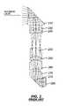
- FIG. 5is a schematic cross section of the elements for the U-shaped layout folded lens from FIG. 4 .
- FIG. 6is a modulation transfer function (MTF) chart for the lens shown in FIGS. 4 and 5 .
- MTFmodulation transfer function
- FIG. 7is a ray trace schematic of a wider angle field of view lens (50 mm EFL) in a Z-shaped layout.
- FIG. 8is a ray trace schematic of a wider angle field of view lens (50 mm EFL) in a U-shaped layout.
- FIG. 9is a schematic cross section of the elements for the U-shaped layout folded lens shown in FIG. 8 .
- FIG. 10is a MTF chart for the lens shown in FIGS. 8 and 9 .
- FIG. 11is a ray trace schematic of a telephoto (107 mm EFL) in a Z-shaped layout.
- FIG. 12is a ray trace schematic of a telephoto lens (107 mm EFL) in a U-shaped layout.
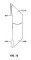
- FIG. 13is a schematic cross section of the elements for the U-shaped layout lens shown in FIG. 12 .
- FIG. 14is a MTF chart for the lens shown in FIGS. 12 and 13 .
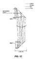
- FIG. 15is schematic cross section of molded-in alignment features at the interface between the two elements for the lens shown in FIGS. 8 and 9 .
- compact sizeis required for portability.
- thinnessis desirable both to reduce size and increase portability, and also to improve the perceived style and improve the heat transfer from the device thereby improving reliability by reducing the operating temperature.
- Folded lens designsprovide an excellent method to reduce the length of an optical assembly.
- the challengeis to deliver high modulation transfer function values out to the Nyquist frequency with a small number of plastic elements that have rotationally symmetric surfaces to keep manufacturing costs low.
- the inventionis based on lens designs with two plastic elements that are mated together to align the elements with each other.
- a planar reflective surfaceis used in each element to turn the optical path by approximately 90 degrees in each element. As such, the planar reflective surfaces do not impart any optical power.
- the optical poweris then delivered by the two refractive surfaces in each element.
- the light rayspass through the refractive surfaces symmetrically so that rotationally symmetric surfaces can be used throughout the lens design.
- the use of rotationally symmetric surfacessubstantially reduces the manufacturing cost of the tooling to make the lens elements.
- the first elementhas positive optical power to reduce the lateral size of the light bundle and the second element has negative optical power to aid in color correction.
- the lens elementsare laid out so that the image sensor plane is parallel to the lens aperture of the first lens surface, which receives the incoming light.
- the advantage of this orientation of the image sensoris that the long dimensions of the image sensor are placed in the lateral dimension of the image capture device so that the image sensor does not add substantially to the thickness of the image capture device.
- FIG. 3shows a two element folded lens design with a Z-shaped layout wherein the incoming light is parallel to the optical axis 355 of the light at the image sensor 360 and the direction of the incoming light is the same as the direction of the light at the image sensor 360 .
- the image sensor 360is located on the back side of the image capture device on the opposite side from the lens aperture which receives the incoming light, with the image sensor 360 facing the front.
- a new lens layoutis proposed in the shape of a U (see FIG. 4 ) wherein the incoming light is parallel to the optical axis 455 of the light at the image sensor 460 but the direction of the incoming light is opposite to the direction of the light at the image sensor 460 .
- the image sensor 460is located on the front side of the image capture device, on the same side if the device as the lens aperture that receives the incoming light, with the image sensor 460 facing the back of the camera or device.
- the thickness of the lens assemblyis reduced compared to a Z-shaped layout because the two horizontal portions of the optical path do not both add to the thickness dimension.
- the horizontal portion of the optical path from the cover glass 305 to the first reflective surface 310 and the horizontal portion of the optical path from the second reflective surface 340 to the image sensor 360both add to the thickness dimension of the lens assembly.
- the horizontal portion of the optical path from the cover glass 305 to the first reflective surface 310 and the horizontal portion of the optical path from the second reflective surface 340 to the image sensor 360both add to the thickness dimension of the lens assembly.
- the horizontal portion of the optical path from the cover glass 305 to the first reflective surface 410 and the horizontal portion of the optical path from the second reflective surface 440 to the image sensor 460do not both add to the thickness dimension since the optical path folds back on itself. Consequently, the U-shaped layout is always thinner than the Z-shaped layout.
- Both the Z-shaped layout and the U-shaped layoutcan be applied to fixed focal length lenses or adjustable focal length (zoom) lenses to reduce the thickness of the lens assembly.
- adjustable focal length lensthe two elements 510 and 520 move relative to one another (in a vertical direction as shown in FIG. 5 ) for zooming.
- a moderate zoom ratiois attainable with this approach.
- the inventionis directed to fixed focal length lens designs.
- a combination of two fixed focal length lenses as described by the invention, a wide angle lens (or moderate angle lens) and a telephoto lens,can be used together in an image module to provide a zoom action with composite imaging.
- the technique of composite imaging to achieve a zoom action with composite imagingis disclosed in commonly-assigned copending U.S. patent application Ser. No. 11/461,574, filed Aug. 1, 2006.
- FIG. 4An exemplary embodiment of the invention for a compact fixed focal length lens with a moderate angle field of view in a U-shaped layout is shown in FIG. 4 .
- This designincludes two prism type elements 510 and 520 with power on one or more refractive surfaces each to produce a very small and thin form factor.
- the U-shaped layoutkeeps the image sensor 460 in an orientation such that the image sensor does not add substantially to the thickness of the lens assembly or the image module that would be produced with the lens assembly.
- the lens design of the inventionalso provides space on either side of the image sensor 460 (above and below the image sensor 460 as shown in FIG.
- FIGS. 3 and 4A cross-sectional view of the two lens elements 510 and 520 for the U-shaped layout is shown in FIG. 5 along with the cover glass 350 and the image sensor 460 .
- Table 1shows the thickness benefit provided by the U-shaped layout as disclosed as the invention as compared to a Z-shaped layout for the moderate angle field of view lens discussed above along with thickness data for a wider angle field of view lens and a telephoto angle field of view lens.
- the ray trace schematics and cross sectional schematics for the wider angle field of view lens in both a Z-shaped layout and a U-shaped layoutare shown in FIGS. 7 , 8 and 9 while the ray trace schematics and cross sectional schematics for the telephoto angle field of view lens in both a Z-shaped layout and a U-shaped layout are shown in FIGS. 11 , 12 and 13 .
- the modulation transfer function chart for the moderate angle field of view lensis shown in FIG. 6 .
- the modulation transfer function provided by the two element folded lens designis quite good out beyond 250 line pairs/mm.
- Nis the Nyquist frequency expressed in line pairs/mm and p is the pixel size in mm.
- the Nyquist charts for the wider angle field of view lens and the telephoto angle field of view lensare shown in FIGS. 10 and 14 respectively.
- the inventionincludes two elements ( 510 and 520 ) that can be different materials to enable color correction and four surfaces ( 400 , 420 , 430 , 450 ) that can be aspheric shape if needed to correct for monochromatic aberrations.
- the inventiondescribes two element lenses that are very small in size, very tight alignment tolerances of the elements with respect to one another are typically required to deliver good modulation transfer function performance.
- the inventionincludes molded-in alignment features 1510 in the plastic elements 1520 and 1530 , at the interface between the two elements, that force the elements 1520 and 1530 into alignment with one another when they are assembled.
- the alignment features 1510are rotationally symmetric so they can be machined along with the optical surfaces.
- the guiding surfaces on the alignment features 1510are preferably angled or tapered to allow the surfaces of the alignment features 1510 to come together easily at first and then get progressively tighter as the elements 1520 and 1530 are moved together into position.
- FIG. 15shows a set of alignment features 1510 associated with the two elements 1520 and 1530 of one of the lens designs discussed previously.
- mounting featurescan also be molded into the two elements. These features can be associated with mounting the lens into the portable device structure or as guidance of the lens during movement for autofocus.
- FIG. 3Ray trace schematics for a lens with moderate angle field of view designed as an example of the invention is shown in a Z-shaped layout in FIG. 3 and a U-shaped layout in FIG. 4 .
- the optical performance and the optical surfacesare the same for both the Z-shaped layout and the U-shaped layout.
- a description of the lens design including surface curvatures, lateral distances, aperture sizes and materialsis given in Table 2 below.
- the lensis designed for an f# of 3.2, a pixel size of 0.002 mm and a sensor with two mega pixels.
- the modulation transfer function chartis shown in FIG. 6 .
- the difference between the Z-shaped layout and the U-shaped layout versions of the lensare in the thickness dimension of the lens assembly, as can be seen in Table 1 and in FIGS.
- the Z-shaped layout lensis 3.84 mm thick while the U-shaped layout lens is only 3.28 mm thick.
- a cross sectional schematic of the U-shaped layout lens assembly with elements 510 and 520 along with cover glass 305 and image sensor 460is shown in FIG. 5 . Based on the sensor size and the thickness, this design is well suited to use in a cell phone or a laptop computer or other application where thinness and moderate angle field of view is important.
- FIG. 7Ray trace schematics for a lens with a wider angle field of view designed as an example of the invention is shown in a Z-shaped layout in FIG. 7 and a U-shaped layout in FIG. 8 .
- the optical performance and the optical surfacesare the same for both the Z-shaped layout and the U-shaped layout.
- a description of the lens design including surface curvatures, lateral distances, aperture sizes and materialsis given in Table 3 below.
- the lensis designed for an f# of 3.2, a pixel size of 0.002 mm and a sensor with two mega pixels.
- the modulation transfer function chartis shown in FIG. 10 .
- the difference between the Z-shaped layout and the U-shaped layout versions of the lensare in the thickness dimension of the lens assembly, as can be seen in Table 1 and in FIGS. 7 and 8 , the Z-shaped layout lens is 3.15 mm thick while the U-shaped layout lens is only 2.56 mm thick.
- a cross sectional schematic of the U-shaped layout lens assembly with elements 910 and 920 along with cover glass 305 and image sensor 460is shown in FIG. 9 . Based on the sensor size and the thickness, this design is well suited to use in a cell phone or a laptop computer or other application where thinness and a wider angle field of view is important.
- Lenses with a telephoto angle field of view lens and a larger image sensorwere designed as yet a further example of the invention.
- Ray trace schematics for a telephoto lens designed as an example of the inventionare shown in a Z-shaped layout in FIG. 11 and a U-shaped layout in FIG. 12 .
- the optical performance and the optical surfacesare the same for both the Z-shaped layout and the U-shaped layout.
- a description of the lens design including surface curvatures, lateral distances, aperture sizes and materialsis given in Table 4 below.
- the lensis designed for an f# of 3.2, a pixel size of 0.003 mm and a sensor with two mega pixels.
- the modulation transfer function chartis shown in FIG. 14 .
- the difference between the Z-shaped layout and the U-shaped layout versions of the lensare in the thickness dimension of the lens assembly, as can be seen in Table 1 and in FIGS. 11 and 12 , the Z-shaped layout lens is 6.34 mm thick while the U-shaped layout lens is only 5.69 mm thick.
- a cross sectional schematic of the U-shaped layout lens assemblyis shown with elements 1310 and 1320 along with cover glass 305 and image sensor 460 in FIG. 13 . Based on the sensor size and the thickness, this design is also well suited to use in a cell phone or a laptop computer or other application where thinness and a telephoto angle field of view is important.
- alignment features 1510guide the two lens elements 1520 and 1530 into a position during assembly wherein the refractive and reflective surfaces are aligned relative to one another.
- the alignment featuresare manufactured at the same time as the refractive and reflective surfaces to improve the accuracy of the relative alignment.
- the lens elements 1510 and 1520are then molded to produce the refractive and reflective surfaces along with the alignment features.
- Other alignment featurescan likewise be manufactured within the scope of the invention along with the refractive and reflective surfaces to aid in aligning the lens into a structural element or to aid in alignment with the image sensor or an autofocus element.
- refractive surface 110reflective surface 120 refractive surface 130 refractive surface 140 reflective surface 150 reflective surface 160 refractive surface 170 infrared filter and cover glass for sensor 180 image sensor 210 prism element 230 refractive element 240 refractive element 250 refractive element 255 refractive element 260 refractive element 270 prism element 275 infrared filter and cover glass for sensor 285 image sensor 305 cover glass 310 reflective surface S2 for moderate angle lens design with Z-shaped layout 340 reflective surface S5 for moderate angle lens design with Z-shaped layout 355 optical axis 360 image sensor 400 refractive surface 410 reflective surface 420 refractive surface 430 refractive surface 440 reflective surface 450 refractive surface 455 optical axis perpendicular to image sensor 460 image sensor 510 first element 520 second element 910 element 920 element 1310 element 1320 element 1510 alignment features 1520 element 1530 element
Landscapes
- Physics & Mathematics (AREA)
- General Physics & Mathematics (AREA)
- Optics & Photonics (AREA)
- Lenses (AREA)
Abstract
Description
| TABLE 1 |
| Thickness comparison of different lens designs |
| Lens type | Lens layout | Thickness (mm) | ||
| Moderate angle | Z | 3.84 | ||
| Moderate angle | U | 3.28 | ||
| Wider angle | Z | 3.15 | ||
| Wider angle | U | 2.56 | ||
| Telephoto | Z | 6.34 | ||
| Telephoto | U | 5.69 | ||
N=1/(2p)
Wherein N is the Nyquist frequency expressed in line pairs/mm and p is the pixel size in mm. The Nyquist charts for the wider angle field of view lens and the telephoto angle field of view lens are shown in
| TABLE 2 |
| Lens description for Example 1 with a 62 mm focal length |
| Thickness or | Aperature | Aperture | |||||
| Element # | Surface # | Radius | Shape | Separation | Dimension | Shape | Material |
| 1 | 1 | Infinite | Flat | 0.3000 | 2.041 | Circular | NBK7 Schott |
| 1 | 2 | Infinite | Flat | 0.1000 | 1.931 | Circular | |
| 2 | 3 | 3.542 | Asphere 1 | 1.3000 | 1.875 | Circular | Zeonex-E48R |
| 2 | 4 | Infinite | Flat | −2.5667 | 3.035 | Circular | Reflective |
| 2 | 5 | 1.834 | Asphere 2 | −0.1000 | 2.574 | Circular | |
| 3 | 6 | 2.369 | Asphere 3 | −2.7595 | 2.467 | Circular | Polycarbonate |
| 3 | 7 | Infinite | Flat | 1.3300 | 4.166 | Circular | Reflective |
| 3 | 8 | 3.642 | Asphere 4 | 0.6667 | 3.709 | Circular | |
| Image | Infinite | Flat | 4.002 | ||||
| Aspheric Constants |
| Z = (VY{circumflex over ( )}2/SQRT(1 + (1 − (1 + K)(C{circumflex over ( )}2Y{circumflex over ( )}2)))) + AY{circumflex over ( )}4 + BY{circumflex over ( )}6 + CY{circumflex over ( )}8 + DY{circumflex over ( )}10 |
| Asphere # | V | K | A | B | C | D |
| Asphere 1 | 2.8240E−01 | 0.0000E+00 | −3.0971E−03 | −8.3905E−04 | 5.6459E−04 | −6.3323E−04 |
| Asphere 2 | 5.4520E−01 | 0.0000E+00 | 6.6605E−03 | −1.9118E−02 | 5.4267E−03 | −1.2105E−03 |
| Asphere 3 | 4.2210E−01 | 0.0000E+00 | 3.6153E−02 | −1.7355E−02 | 5.9225E−03 | −1.0372E−03 |
| Asphere 4 | 2.7460E−01 | 0.0000E+00 | −1.3189E−02 | −1.3661E−03 | 5.9801E−04 | −4.8621E−05 |
| TABLE 3 |
| Lens description for Example 2 with a 62 mm focal length |
| Thickness or | Aperature | Aperture | |||||
| Element # | Surface # | Radius | Shape | Separation | Dimension | Shape | Material |
| 1 | 1 | Infinite | Flat | 0.3000 | 1.732 | Circular | NBK7 Schott |
| 1 | 2 | Infinite | Flat | 0.1000 | 1.596 | Circular | |
| 2 | 3 | 2.182 | Asphere 1 | 1.2000 | 1.444 | Circular | Zeonex-E48R |
| 2 | 4 | Infinite | Flat | −1.8700 | 2.339 | Circular | Reflective |
| 2 | 5 | 1.270 | Asphere 2 | −0.1728 | 2.015 | Circular | |
| 3 | 6 | 1.164 | Asphere 3 | −1.0500 | 1.941 | Circular | Polycarbonate |
| 3 | 7 | Infinite | Flat | 1.0500 | 3.880 | Circular | Reflective |
| 3 | 8 | 2.837 | Asphere 4 | 0.5000 | 3.311 | Circular | |
| Image | Infinite | Flat | 3.496 | ||||
| Aspheric Constants |
| Z = (VY{circumflex over ( )}2/SQRT(1 + (1 − (1 + K)(C{circumflex over ( )}2Y{circumflex over ( )}2)))) + AY{circumflex over ( )}4 + BY{circumflex over ( )}6 + CY{circumflex over ( )}8 + DY{circumflex over ( )}10 |
| Asphere # | V | K | A | B | C | D |
| Asphere 1 | 4.5820E−01 | 0.0000E+00 | −5.6310E−03 | −2.5584E−03 | 1.9920E−03 | −6.4583E−03 |
| Asphere 2 | 7.8720E−01 | 0.0000E+00 | 2.3760E−02 | −2.1772E−02 | 1.9544E−01 | −7.2848E−02 |
| Asphere 3 | 8.5920E−01 | 0.0000E+00 | 1.4551E−01 | −4.4757E−01 | 4.4868E−01 | −1.8946E−01 |
| Asphere 4 | 3.5250E−01 | 0.0000E+00 | −1.3026E−01 | 4.6514E−02 | −1.3216E−02 | 1.4327E−03 |
| TABLE 4 |
| Lens description for Example 3 with a 107 mm focal length |
| Thickness or | Aperature | Aperture | |||||
| Element # | Surface # | Radius | Shape | Separation | Dimension | Shape | Material |
| 1 | 1 | Infinite | Flat | 0.3000 | 4.784 | Circular | NBK7 Schott |
| 1 | 2 | Infinite | Flat | 0.1000 | 4.72 | Circular | |
| 2 | 3 | 8.008 | Asphere 1 | 2.7500 | 4.688 | Circular | Zeonex-E48R |
| 2 | 4 | Infinite | Flat | −7.0040 | 6.754 | Circular | Reflective |
| 2 | 5 | 4.273 | Asphere 2 | −0.1000 | 4.905 | Circular | |
| 3 | 6 | 4.93 | Asphere 3 | −9.0612 | 4.767 | Circular | Polycarbonate |
| 3 | 7 | Infinite | Flat | 2.0000 | 6.51 | Circular | Reflective |
| 3 | 8 | 8.628 | Asphere 4 | 1.0000 | 5.622 | Circular | |
| Image | Infinite | Flat | 6.001 | ||||
| Aspheric Constants |
| Z = (VY{circumflex over ( )}2/SQRT(1 + (1 − (1 + K)(C{circumflex over ( )}2Y{circumflex over ( )}2)))) + AY{circumflex over ( )}4 + BY{circumflex over ( )}6 + CY{circumflex over ( )}8 + DY{circumflex over ( )}10 |
| Asphere # | V | K | A | B | C | D |
| Asphere 1 | 1.2490E−01 | 0.0000E+00 | −1.1073E−04 | −5.7443E−06 | 5.8261E−07 | −7.2893E−08 |
| Asphere 2 | 2.3410E−01 | 0.0000E+00 | −3.5903E−04 | −2.7866E−04 | 2.7053E−05 | −1.5048E−06 |
| Asphere 3 | 2.0290E−01 | 0.0000E+00 | 1.2061E−03 | −2.4682E−04 | 2.7606E−05 | −1.4681E−06 |
| Asphere 4 | 1.1590E−01 | 0.0000E+00 | −6.5592E−04 | 1.1303E−04 | −2.3992E−05 | 2.3945E−06 |
| 100 | |
| 110 | |
| 120 | |
| 130 | |
| 140 | |
| 150 | |
| 160 | |
| 170 | infrared filter and cover glass for |
| 180 | |
| 210 | |
| 230 | |
| 240 | |
| 250 | |
| 255 | |
| 260 | |
| 270 | |
| 275 | infrared filter and cover glass for |
| 285 | |
| 305 | |
| 310 | reflective surface S2 for moderate angle |
| lens design with Z-shaped | |
| 340 | reflective surface S5 for moderate angle |
| lens design with Z-shaped | |
| 355 | |
| 360 | |
| 400 | |
| 410 | |
| 420 | |
| 430 | |
| 440 | |
| 450 | |
| 455 | optical axis perpendicular to |
| 460 | |
| 510 | |
| 520 | |
| 910 | |
| 920 | |
| 1310 | |
| 1320 | |
| 1510 | alignment features |
| 1520 | |
| 1530 | element |
Claims (8)
Priority Applications (2)
| Application Number | Priority Date | Filing Date | Title |
|---|---|---|---|
| US11/961,038US7616393B2 (en) | 2007-12-20 | 2007-12-20 | Compact folded thin lens |
| PCT/US2008/013613WO2009085120A1 (en) | 2007-12-20 | 2008-12-11 | A compact folded thin lens |
Applications Claiming Priority (1)
| Application Number | Priority Date | Filing Date | Title |
|---|---|---|---|
| US11/961,038US7616393B2 (en) | 2007-12-20 | 2007-12-20 | Compact folded thin lens |
Publications (2)
| Publication Number | Publication Date |
|---|---|
| US20090161235A1 US20090161235A1 (en) | 2009-06-25 |
| US7616393B2true US7616393B2 (en) | 2009-11-10 |
Family
ID=40404799
Family Applications (1)
| Application Number | Title | Priority Date | Filing Date |
|---|---|---|---|
| US11/961,038Expired - Fee RelatedUS7616393B2 (en) | 2007-12-20 | 2007-12-20 | Compact folded thin lens |
Country Status (2)
| Country | Link |
|---|---|
| US (1) | US7616393B2 (en) |
| WO (1) | WO2009085120A1 (en) |
Cited By (11)
| Publication number | Priority date | Publication date | Assignee | Title |
|---|---|---|---|---|
| US20130113979A1 (en)* | 2011-11-08 | 2013-05-09 | Hoya Corporation | Imaging unit |
| US20130260823A1 (en)* | 2012-03-31 | 2013-10-03 | Ashutosh Y. Shukla | Compact Portable Electronic Device Having Augmented Back Volume for Speaker |
| US8835825B2 (en) | 2012-08-14 | 2014-09-16 | Symbol Technologies, Inc. | High performance scan engine with rear-facing image sensor in handheld arrangement for, and method of, imaging targets using the scan engine |
| US9064765B2 (en) | 2012-08-14 | 2015-06-23 | Symbol Technologies, Llc | Handheld imaging apparatus for, and method of, imaging targets using a high performance, compact scan engine |
| US9172856B2 (en) | 2011-03-29 | 2015-10-27 | Microsoft Technology Licensing, Llc | Folded imaging path camera |
| US10386605B2 (en) | 2016-07-14 | 2019-08-20 | Largan Precision Co., Ltd. | Optical photographing assembly, image capturing apparatus, and electronic device comprising five-lens system having inflection point |
| US10788651B2 (en) | 2015-11-13 | 2020-09-29 | Samsung Electronics Co., Ltd. | Tele-lens and imaging device |
| US11029496B2 (en) | 2017-12-21 | 2021-06-08 | Apple Inc. | Folded lens system |
| EP4209817A1 (en)* | 2015-02-27 | 2023-07-12 | Adeia Imaging LLC | An optical system for an image acquisition device |
| US11933949B2 (en) | 2019-09-27 | 2024-03-19 | Apple Inc. | Freeform folded optical system |
| US12032146B2 (en) | 2018-09-25 | 2024-07-09 | Apple Inc. | Camera lens system |
Families Citing this family (7)
| Publication number | Priority date | Publication date | Assignee | Title |
|---|---|---|---|---|
| DE102010033425A1 (en)* | 2010-08-04 | 2012-02-09 | Karl Storz Gmbh & Co. Kg | Endoscope with adjustable viewing direction |
| US9037094B2 (en) | 2011-10-17 | 2015-05-19 | Golba Llc | Method and system for high-throughput and low-power communication links in a distributed transceiver network |
| US9197982B2 (en) | 2012-08-08 | 2015-11-24 | Golba Llc | Method and system for distributed transceivers for distributed access points connectivity |
| US10437022B2 (en) | 2016-03-28 | 2019-10-08 | Apple Inc. | Folded lens system with five refractive lenses |
| US10484078B2 (en) | 2017-07-11 | 2019-11-19 | Movandi Corporation | Reconfigurable and modular active repeater device |
| TWI730637B (en)* | 2020-02-24 | 2021-06-11 | 大陽科技股份有限公司 | Camera module and electronic device |
| EP4229461A1 (en)* | 2020-12-15 | 2023-08-23 | Huawei Technologies Co., Ltd. | Optical magnification device for electronic apparatus |
Citations (13)
| Publication number | Priority date | Publication date | Assignee | Title |
|---|---|---|---|---|
| US4941731A (en) | 1987-07-01 | 1990-07-17 | John Macken | Corner cube utilizing generally spherical surfaces |
| US6278553B1 (en) | 1998-02-27 | 2001-08-21 | Canon Kabushiki Kaisha | Optical system having refractive index distribution |
| US20030076436A1 (en) | 2001-10-16 | 2003-04-24 | Victor Company Of Japan, Ltd | Image forming optical device and image sensing device |
| US6795253B2 (en) | 2002-05-08 | 2004-09-21 | Fuji Photo Optical Co., Ltd. | Imaging lens |
| US20050002073A1 (en)* | 2000-09-29 | 2005-01-06 | Olympus Corporation | Observation optical system using volume hologram |
| US6842295B2 (en) | 2002-03-29 | 2005-01-11 | Fuji Photo Optical Co., Ltd. | Imaging lens formed of aperture diaphragm and only two lens components |
| US6898023B2 (en) | 2002-07-22 | 2005-05-24 | Nidec Copal Corporation | Zoom lens |
| US6900950B2 (en) | 2000-12-25 | 2005-05-31 | Olympus Corporation | Image-forming optical system |
| US6961191B2 (en) | 2003-03-31 | 2005-11-01 | Fujinon Corporation | Single focus lens |
| US20060092524A1 (en) | 2004-10-29 | 2006-05-04 | Konica Minolta Opto, Inc. | Zoom optical system, imaging lens device, and digital apparatus |
| US20060279821A1 (en)* | 2005-05-26 | 2006-12-14 | Inphase Technologies, Inc. | Holographic drive head alignments |
| US7221522B2 (en)* | 2005-01-28 | 2007-05-22 | Karl Storz Development Corp. | Optical system for variable direction of view instrument |
| US20080291531A1 (en) | 2006-10-09 | 2008-11-27 | Heimer Richard J | Compact Objective Lens Assembly |
- 2007
- 2007-12-20USUS11/961,038patent/US7616393B2/ennot_activeExpired - Fee Related
- 2008
- 2008-12-11WOPCT/US2008/013613patent/WO2009085120A1/enactiveApplication Filing
Patent Citations (13)
| Publication number | Priority date | Publication date | Assignee | Title |
|---|---|---|---|---|
| US4941731A (en) | 1987-07-01 | 1990-07-17 | John Macken | Corner cube utilizing generally spherical surfaces |
| US6278553B1 (en) | 1998-02-27 | 2001-08-21 | Canon Kabushiki Kaisha | Optical system having refractive index distribution |
| US20050002073A1 (en)* | 2000-09-29 | 2005-01-06 | Olympus Corporation | Observation optical system using volume hologram |
| US6900950B2 (en) | 2000-12-25 | 2005-05-31 | Olympus Corporation | Image-forming optical system |
| US20030076436A1 (en) | 2001-10-16 | 2003-04-24 | Victor Company Of Japan, Ltd | Image forming optical device and image sensing device |
| US6842295B2 (en) | 2002-03-29 | 2005-01-11 | Fuji Photo Optical Co., Ltd. | Imaging lens formed of aperture diaphragm and only two lens components |
| US6795253B2 (en) | 2002-05-08 | 2004-09-21 | Fuji Photo Optical Co., Ltd. | Imaging lens |
| US6898023B2 (en) | 2002-07-22 | 2005-05-24 | Nidec Copal Corporation | Zoom lens |
| US6961191B2 (en) | 2003-03-31 | 2005-11-01 | Fujinon Corporation | Single focus lens |
| US20060092524A1 (en) | 2004-10-29 | 2006-05-04 | Konica Minolta Opto, Inc. | Zoom optical system, imaging lens device, and digital apparatus |
| US7221522B2 (en)* | 2005-01-28 | 2007-05-22 | Karl Storz Development Corp. | Optical system for variable direction of view instrument |
| US20060279821A1 (en)* | 2005-05-26 | 2006-12-14 | Inphase Technologies, Inc. | Holographic drive head alignments |
| US20080291531A1 (en) | 2006-10-09 | 2008-11-27 | Heimer Richard J | Compact Objective Lens Assembly |
Cited By (16)
| Publication number | Priority date | Publication date | Assignee | Title |
|---|---|---|---|---|
| US9172856B2 (en) | 2011-03-29 | 2015-10-27 | Microsoft Technology Licensing, Llc | Folded imaging path camera |
| US20130113979A1 (en)* | 2011-11-08 | 2013-05-09 | Hoya Corporation | Imaging unit |
| US8836856B2 (en)* | 2011-11-08 | 2014-09-16 | Hoya Corporation | Imaging unit with prisms and image sensor |
| US20130260823A1 (en)* | 2012-03-31 | 2013-10-03 | Ashutosh Y. Shukla | Compact Portable Electronic Device Having Augmented Back Volume for Speaker |
| US8835825B2 (en) | 2012-08-14 | 2014-09-16 | Symbol Technologies, Inc. | High performance scan engine with rear-facing image sensor in handheld arrangement for, and method of, imaging targets using the scan engine |
| US9064765B2 (en) | 2012-08-14 | 2015-06-23 | Symbol Technologies, Llc | Handheld imaging apparatus for, and method of, imaging targets using a high performance, compact scan engine |
| EP4209817A1 (en)* | 2015-02-27 | 2023-07-12 | Adeia Imaging LLC | An optical system for an image acquisition device |
| US10788651B2 (en) | 2015-11-13 | 2020-09-29 | Samsung Electronics Co., Ltd. | Tele-lens and imaging device |
| US10732389B2 (en) | 2016-07-14 | 2020-08-04 | Largan Precision Co., Ltd. | Optical photographing assembly, image capturing apparatus and electronic device having aspheric lens element with inflection point |
| US11520123B2 (en) | 2016-07-14 | 2022-12-06 | Largan Precision Co., Ltd. | Optical photographing assembly having five lenses and specified abbe number |
| US10386605B2 (en) | 2016-07-14 | 2019-08-20 | Largan Precision Co., Ltd. | Optical photographing assembly, image capturing apparatus, and electronic device comprising five-lens system having inflection point |
| US11789243B2 (en) | 2016-07-14 | 2023-10-17 | Largan Precision Co., Ltd. | Optical photographing assembly having five lenses and specified field of view |
| US11029496B2 (en) | 2017-12-21 | 2021-06-08 | Apple Inc. | Folded lens system |
| US11899186B2 (en) | 2017-12-21 | 2024-02-13 | Apple Inc. | Folded lens system |
| US12032146B2 (en) | 2018-09-25 | 2024-07-09 | Apple Inc. | Camera lens system |
| US11933949B2 (en) | 2019-09-27 | 2024-03-19 | Apple Inc. | Freeform folded optical system |
Also Published As
| Publication number | Publication date |
|---|---|
| US20090161235A1 (en) | 2009-06-25 |
| WO2009085120A1 (en) | 2009-07-09 |
Similar Documents
| Publication | Publication Date | Title |
|---|---|---|
| US7616393B2 (en) | Compact folded thin lens | |
| US11681126B2 (en) | Optical imaging system and portable electronic device including the same | |
| US11733490B2 (en) | Optical system | |
| US11442256B2 (en) | Imaging optical lens assembly, imaging apparatus and electronic device | |
| US7605986B2 (en) | Zoom lens | |
| US11921269B2 (en) | Optical imaging device | |
| US9377604B2 (en) | Zoom lens and electronic apparatus having the same | |
| US20250102774A1 (en) | Optical system, lens module, and electronic device | |
| US20230314773A1 (en) | Optical system | |
| US20250306344A1 (en) | Optical imaging system | |
| EP4194920A1 (en) | Optical system | |
| US7457048B2 (en) | High magnification zoom lens system | |
| CN119045171A (en) | Optical lens, camera module and electronic equipment | |
| US9645368B2 (en) | Zoom lens | |
| EP4435488A1 (en) | Optical imaging system, camera module and electronic device | |
| CN216561186U (en) | Hybrid lens system, imaging apparatus, and electronic apparatus | |
| CN117572612B (en) | Zoom lens system and camera | |
| US20240094509A1 (en) | Optical system | |
| US20250298220A1 (en) | Image capturing optical system, imaging apparatus and electronic device | |
| US20250216746A1 (en) | Optical system, lens module, and electronic device | |
| CN102759791B (en) | Zoom lens | |
| CN116909003A (en) | Zoom optical system | |
| CN120103587A (en) | Optical lenses, camera modules and electronic devices | |
| TW202235944A (en) | Optical system | |
| CN118175403A (en) | Camera system, camera and mobile terminal |
Legal Events
| Date | Code | Title | Description |
|---|---|---|---|
| AS | Assignment | Owner name:EASTMAN KODAK COMPANY, NEW YORK Free format text:ASSIGNMENT OF ASSIGNORS INTEREST;ASSIGNORS:BORDER, JOHN N.;BIETRY, JOSEPH R.;COMPTON, JOHN T.;REEL/FRAME:020276/0097;SIGNING DATES FROM 20071218 TO 20071220 Owner name:EASTMAN KODAK COMPANY,NEW YORK Free format text:ASSIGNMENT OF ASSIGNORS INTEREST;ASSIGNORS:BORDER, JOHN N.;BIETRY, JOSEPH R.;COMPTON, JOHN T.;SIGNING DATES FROM 20071218 TO 20071220;REEL/FRAME:020276/0097 | |
| FEPP | Fee payment procedure | Free format text:PAYOR NUMBER ASSIGNED (ORIGINAL EVENT CODE: ASPN); ENTITY STATUS OF PATENT OWNER: LARGE ENTITY | |
| STCF | Information on status: patent grant | Free format text:PATENTED CASE | |
| AS | Assignment | Owner name:CITICORP NORTH AMERICA, INC., AS AGENT, NEW YORK Free format text:SECURITY INTEREST;ASSIGNORS:EASTMAN KODAK COMPANY;PAKON, INC.;REEL/FRAME:028201/0420 Effective date:20120215 | |
| AS | Assignment | Owner name:NPEC INC., NEW YORK Free format text:PATENT RELEASE;ASSIGNORS:CITICORP NORTH AMERICA, INC.;WILMINGTON TRUST, NATIONAL ASSOCIATION;REEL/FRAME:029913/0001 Effective date:20130201 Owner name:KODAK AMERICAS, LTD., NEW YORK Free format text:PATENT RELEASE;ASSIGNORS:CITICORP NORTH AMERICA, INC.;WILMINGTON TRUST, NATIONAL ASSOCIATION;REEL/FRAME:029913/0001 Effective date:20130201 Owner name:CREO MANUFACTURING AMERICA LLC, WYOMING Free format text:PATENT RELEASE;ASSIGNORS:CITICORP NORTH AMERICA, INC.;WILMINGTON TRUST, NATIONAL ASSOCIATION;REEL/FRAME:029913/0001 Effective date:20130201 Owner name:KODAK IMAGING NETWORK, INC., CALIFORNIA Free format text:PATENT RELEASE;ASSIGNORS:CITICORP NORTH AMERICA, INC.;WILMINGTON TRUST, NATIONAL ASSOCIATION;REEL/FRAME:029913/0001 Effective date:20130201 Owner name:EASTMAN KODAK INTERNATIONAL CAPITAL COMPANY, INC., Free format text:PATENT RELEASE;ASSIGNORS:CITICORP NORTH AMERICA, INC.;WILMINGTON TRUST, NATIONAL ASSOCIATION;REEL/FRAME:029913/0001 Effective date:20130201 Owner name:KODAK AVIATION LEASING LLC, NEW YORK Free format text:PATENT RELEASE;ASSIGNORS:CITICORP NORTH AMERICA, INC.;WILMINGTON TRUST, NATIONAL ASSOCIATION;REEL/FRAME:029913/0001 Effective date:20130201 Owner name:FAR EAST DEVELOPMENT LTD., NEW YORK Free format text:PATENT RELEASE;ASSIGNORS:CITICORP NORTH AMERICA, INC.;WILMINGTON TRUST, NATIONAL ASSOCIATION;REEL/FRAME:029913/0001 Effective date:20130201 Owner name:KODAK REALTY, INC., NEW YORK Free format text:PATENT RELEASE;ASSIGNORS:CITICORP NORTH AMERICA, INC.;WILMINGTON TRUST, NATIONAL ASSOCIATION;REEL/FRAME:029913/0001 Effective date:20130201 Owner name:KODAK (NEAR EAST), INC., NEW YORK Free format text:PATENT RELEASE;ASSIGNORS:CITICORP NORTH AMERICA, INC.;WILMINGTON TRUST, NATIONAL ASSOCIATION;REEL/FRAME:029913/0001 Effective date:20130201 Owner name:LASER-PACIFIC MEDIA CORPORATION, NEW YORK Free format text:PATENT RELEASE;ASSIGNORS:CITICORP NORTH AMERICA, INC.;WILMINGTON TRUST, NATIONAL ASSOCIATION;REEL/FRAME:029913/0001 Effective date:20130201 Owner name:FPC INC., CALIFORNIA Free format text:PATENT RELEASE;ASSIGNORS:CITICORP NORTH AMERICA, INC.;WILMINGTON TRUST, NATIONAL ASSOCIATION;REEL/FRAME:029913/0001 Effective date:20130201 Owner name:KODAK PHILIPPINES, LTD., NEW YORK Free format text:PATENT RELEASE;ASSIGNORS:CITICORP NORTH AMERICA, INC.;WILMINGTON TRUST, NATIONAL ASSOCIATION;REEL/FRAME:029913/0001 Effective date:20130201 Owner name:PAKON, INC., INDIANA Free format text:PATENT RELEASE;ASSIGNORS:CITICORP NORTH AMERICA, INC.;WILMINGTON TRUST, NATIONAL ASSOCIATION;REEL/FRAME:029913/0001 Effective date:20130201 Owner name:QUALEX INC., NORTH CAROLINA Free format text:PATENT RELEASE;ASSIGNORS:CITICORP NORTH AMERICA, INC.;WILMINGTON TRUST, NATIONAL ASSOCIATION;REEL/FRAME:029913/0001 Effective date:20130201 Owner name:EASTMAN KODAK COMPANY, NEW YORK Free format text:PATENT RELEASE;ASSIGNORS:CITICORP NORTH AMERICA, INC.;WILMINGTON TRUST, NATIONAL ASSOCIATION;REEL/FRAME:029913/0001 Effective date:20130201 Owner name:KODAK PORTUGUESA LIMITED, NEW YORK Free format text:PATENT RELEASE;ASSIGNORS:CITICORP NORTH AMERICA, INC.;WILMINGTON TRUST, NATIONAL ASSOCIATION;REEL/FRAME:029913/0001 Effective date:20130201 | |
| FPAY | Fee payment | Year of fee payment:4 | |
| AS | Assignment | Owner name:INTELLECTUAL VENTURES FUND 83 LLC, NEVADA Free format text:ASSIGNMENT OF ASSIGNORS INTEREST;ASSIGNOR:EASTMAN KODAK COMPANY;REEL/FRAME:030215/0289 Effective date:20130201 | |
| AS | Assignment | Owner name:MONUMENT PEAK VENTURES, LLC, TEXAS Free format text:ASSIGNMENT OF ASSIGNORS INTEREST;ASSIGNOR:INTELLECTUAL VENTURES FUND 83 LLC;REEL/FRAME:041941/0079 Effective date:20170215 | |
| REMI | Maintenance fee reminder mailed | ||
| FEPP | Fee payment procedure | Free format text:7.5 YR SURCHARGE - LATE PMT W/IN 6 MO, LARGE ENTITY (ORIGINAL EVENT CODE: M1555) | |
| MAFP | Maintenance fee payment | Free format text:PAYMENT OF MAINTENANCE FEE, 8TH YEAR, LARGE ENTITY (ORIGINAL EVENT CODE: M1552) Year of fee payment:8 | |
| FEPP | Fee payment procedure | Free format text:MAINTENANCE FEE REMINDER MAILED (ORIGINAL EVENT CODE: REM.); ENTITY STATUS OF PATENT OWNER: LARGE ENTITY | |
| LAPS | Lapse for failure to pay maintenance fees | Free format text:PATENT EXPIRED FOR FAILURE TO PAY MAINTENANCE FEES (ORIGINAL EVENT CODE: EXP.); ENTITY STATUS OF PATENT OWNER: LARGE ENTITY | |
| STCH | Information on status: patent discontinuation | Free format text:PATENT EXPIRED DUE TO NONPAYMENT OF MAINTENANCE FEES UNDER 37 CFR 1.362 | |
| FP | Lapsed due to failure to pay maintenance fee | Effective date:20211110 | |
| AS | Assignment | Owner name:MONUMENT PEAK VENTURES, LLC, TEXAS Free format text:RELEASE BY SECURED PARTY;ASSIGNOR:INTELLECTUAL VENTURES FUND 83 LLC;REEL/FRAME:064599/0304 Effective date:20230728 |