US7615462B2 - Etch stop layer for silicon (Si) via etch in three-dimensional (3-D) wafer-to-wafer vertical stack - Google Patents
Etch stop layer for silicon (Si) via etch in three-dimensional (3-D) wafer-to-wafer vertical stackDownload PDFInfo
- Publication number
- US7615462B2 US7615462B2US11/528,986US52898606AUS7615462B2US 7615462 B2US7615462 B2US 7615462B2US 52898606 AUS52898606 AUS 52898606AUS 7615462 B2US7615462 B2US 7615462B2
- Authority
- US
- United States
- Prior art keywords
- forming
- layer
- wafer
- etch stop
- silicon
- Prior art date
- Legal status (The legal status is an assumption and is not a legal conclusion. Google has not performed a legal analysis and makes no representation as to the accuracy of the status listed.)
- Expired - Fee Related, expires
Links
Images


Classifications
- H—ELECTRICITY
- H01—ELECTRIC ELEMENTS
- H01L—SEMICONDUCTOR DEVICES NOT COVERED BY CLASS H10
- H01L21/00—Processes or apparatus adapted for the manufacture or treatment of semiconductor or solid state devices or of parts thereof
- H01L21/02—Manufacture or treatment of semiconductor devices or of parts thereof
- H01L21/04—Manufacture or treatment of semiconductor devices or of parts thereof the devices having potential barriers, e.g. a PN junction, depletion layer or carrier concentration layer
- H01L21/18—Manufacture or treatment of semiconductor devices or of parts thereof the devices having potential barriers, e.g. a PN junction, depletion layer or carrier concentration layer the devices having semiconductor bodies comprising elements of Group IV of the Periodic Table or AIIIBV compounds with or without impurities, e.g. doping materials
- H01L21/30—Treatment of semiconductor bodies using processes or apparatus not provided for in groups H01L21/20 - H01L21/26
- H01L21/302—Treatment of semiconductor bodies using processes or apparatus not provided for in groups H01L21/20 - H01L21/26 to change their surface-physical characteristics or shape, e.g. etching, polishing, cutting
- H01L21/306—Chemical or electrical treatment, e.g. electrolytic etching
- H01L21/30604—Chemical etching
- H—ELECTRICITY
- H01—ELECTRIC ELEMENTS
- H01L—SEMICONDUCTOR DEVICES NOT COVERED BY CLASS H10
- H01L21/00—Processes or apparatus adapted for the manufacture or treatment of semiconductor or solid state devices or of parts thereof
- H01L21/02—Manufacture or treatment of semiconductor devices or of parts thereof
- H01L21/04—Manufacture or treatment of semiconductor devices or of parts thereof the devices having potential barriers, e.g. a PN junction, depletion layer or carrier concentration layer
- H01L21/18—Manufacture or treatment of semiconductor devices or of parts thereof the devices having potential barriers, e.g. a PN junction, depletion layer or carrier concentration layer the devices having semiconductor bodies comprising elements of Group IV of the Periodic Table or AIIIBV compounds with or without impurities, e.g. doping materials
- H01L21/30—Treatment of semiconductor bodies using processes or apparatus not provided for in groups H01L21/20 - H01L21/26
- H01L21/302—Treatment of semiconductor bodies using processes or apparatus not provided for in groups H01L21/20 - H01L21/26 to change their surface-physical characteristics or shape, e.g. etching, polishing, cutting
- H01L21/306—Chemical or electrical treatment, e.g. electrolytic etching
- H01L21/3065—Plasma etching; Reactive-ion etching
- H—ELECTRICITY
- H01—ELECTRIC ELEMENTS
- H01L—SEMICONDUCTOR DEVICES NOT COVERED BY CLASS H10
- H01L21/00—Processes or apparatus adapted for the manufacture or treatment of semiconductor or solid state devices or of parts thereof
- H01L21/70—Manufacture or treatment of devices consisting of a plurality of solid state components formed in or on a common substrate or of parts thereof; Manufacture of integrated circuit devices or of parts thereof
- H01L21/71—Manufacture of specific parts of devices defined in group H01L21/70
- H01L21/768—Applying interconnections to be used for carrying current between separate components within a device comprising conductors and dielectrics
- H01L21/76898—Applying interconnections to be used for carrying current between separate components within a device comprising conductors and dielectrics formed through a semiconductor substrate
- H—ELECTRICITY
- H01—ELECTRIC ELEMENTS
- H01L—SEMICONDUCTOR DEVICES NOT COVERED BY CLASS H10
- H01L23/00—Details of semiconductor or other solid state devices
- H01L23/48—Arrangements for conducting electric current to or from the solid state body in operation, e.g. leads, terminal arrangements ; Selection of materials therefor
- H01L23/481—Internal lead connections, e.g. via connections, feedthrough structures
- H—ELECTRICITY
- H01—ELECTRIC ELEMENTS
- H01L—SEMICONDUCTOR DEVICES NOT COVERED BY CLASS H10
- H01L24/00—Arrangements for connecting or disconnecting semiconductor or solid-state bodies; Methods or apparatus related thereto
- H01L24/80—Methods for connecting semiconductor or other solid state bodies using means for bonding being attached to, or being formed on, the surface to be connected
- H01L24/81—Methods for connecting semiconductor or other solid state bodies using means for bonding being attached to, or being formed on, the surface to be connected using a bump connector
- H—ELECTRICITY
- H01—ELECTRIC ELEMENTS
- H01L—SEMICONDUCTOR DEVICES NOT COVERED BY CLASS H10
- H01L25/00—Assemblies consisting of a plurality of semiconductor or other solid state devices
- H01L25/03—Assemblies consisting of a plurality of semiconductor or other solid state devices all the devices being of a type provided for in a single subclass of subclasses H10B, H10D, H10F, H10H, H10K or H10N, e.g. assemblies of rectifier diodes
- H01L25/04—Assemblies consisting of a plurality of semiconductor or other solid state devices all the devices being of a type provided for in a single subclass of subclasses H10B, H10D, H10F, H10H, H10K or H10N, e.g. assemblies of rectifier diodes the devices not having separate containers
- H01L25/065—Assemblies consisting of a plurality of semiconductor or other solid state devices all the devices being of a type provided for in a single subclass of subclasses H10B, H10D, H10F, H10H, H10K or H10N, e.g. assemblies of rectifier diodes the devices not having separate containers the devices being of a type provided for in group H10D89/00
- H01L25/0657—Stacked arrangements of devices
- H—ELECTRICITY
- H01—ELECTRIC ELEMENTS
- H01L—SEMICONDUCTOR DEVICES NOT COVERED BY CLASS H10
- H01L25/00—Assemblies consisting of a plurality of semiconductor or other solid state devices
- H01L25/50—Multistep manufacturing processes of assemblies consisting of devices, the devices being individual devices of subclass H10D or integrated devices of class H10
- H—ELECTRICITY
- H01—ELECTRIC ELEMENTS
- H01L—SEMICONDUCTOR DEVICES NOT COVERED BY CLASS H10
- H01L2224/00—Indexing scheme for arrangements for connecting or disconnecting semiconductor or solid-state bodies and methods related thereto as covered by H01L24/00
- H01L2224/01—Means for bonding being attached to, or being formed on, the surface to be connected, e.g. chip-to-package, die-attach, "first-level" interconnects; Manufacturing methods related thereto
- H01L2224/10—Bump connectors; Manufacturing methods related thereto
- H01L2224/12—Structure, shape, material or disposition of the bump connectors prior to the connecting process
- H01L2224/13—Structure, shape, material or disposition of the bump connectors prior to the connecting process of an individual bump connector
- H01L2224/13001—Core members of the bump connector
- H01L2224/13099—Material
- H01L2224/131—Material with a principal constituent of the material being a metal or a metalloid, e.g. boron [B], silicon [Si], germanium [Ge], arsenic [As], antimony [Sb], tellurium [Te] and polonium [Po], and alloys thereof
- H01L2224/13138—Material with a principal constituent of the material being a metal or a metalloid, e.g. boron [B], silicon [Si], germanium [Ge], arsenic [As], antimony [Sb], tellurium [Te] and polonium [Po], and alloys thereof the principal constituent melting at a temperature of greater than or equal to 950°C and less than 1550°C
- H01L2224/13139—Silver [Ag] as principal constituent
- H—ELECTRICITY
- H01—ELECTRIC ELEMENTS
- H01L—SEMICONDUCTOR DEVICES NOT COVERED BY CLASS H10
- H01L2224/00—Indexing scheme for arrangements for connecting or disconnecting semiconductor or solid-state bodies and methods related thereto as covered by H01L24/00
- H01L2224/01—Means for bonding being attached to, or being formed on, the surface to be connected, e.g. chip-to-package, die-attach, "first-level" interconnects; Manufacturing methods related thereto
- H01L2224/10—Bump connectors; Manufacturing methods related thereto
- H01L2224/12—Structure, shape, material or disposition of the bump connectors prior to the connecting process
- H01L2224/13—Structure, shape, material or disposition of the bump connectors prior to the connecting process of an individual bump connector
- H01L2224/13001—Core members of the bump connector
- H01L2224/13099—Material
- H01L2224/131—Material with a principal constituent of the material being a metal or a metalloid, e.g. boron [B], silicon [Si], germanium [Ge], arsenic [As], antimony [Sb], tellurium [Te] and polonium [Po], and alloys thereof
- H01L2224/13138—Material with a principal constituent of the material being a metal or a metalloid, e.g. boron [B], silicon [Si], germanium [Ge], arsenic [As], antimony [Sb], tellurium [Te] and polonium [Po], and alloys thereof the principal constituent melting at a temperature of greater than or equal to 950°C and less than 1550°C
- H01L2224/13144—Gold [Au] as principal constituent
- H—ELECTRICITY
- H01—ELECTRIC ELEMENTS
- H01L—SEMICONDUCTOR DEVICES NOT COVERED BY CLASS H10
- H01L2224/00—Indexing scheme for arrangements for connecting or disconnecting semiconductor or solid-state bodies and methods related thereto as covered by H01L24/00
- H01L2224/01—Means for bonding being attached to, or being formed on, the surface to be connected, e.g. chip-to-package, die-attach, "first-level" interconnects; Manufacturing methods related thereto
- H01L2224/10—Bump connectors; Manufacturing methods related thereto
- H01L2224/12—Structure, shape, material or disposition of the bump connectors prior to the connecting process
- H01L2224/13—Structure, shape, material or disposition of the bump connectors prior to the connecting process of an individual bump connector
- H01L2224/13001—Core members of the bump connector
- H01L2224/13099—Material
- H01L2224/131—Material with a principal constituent of the material being a metal or a metalloid, e.g. boron [B], silicon [Si], germanium [Ge], arsenic [As], antimony [Sb], tellurium [Te] and polonium [Po], and alloys thereof
- H01L2224/13138—Material with a principal constituent of the material being a metal or a metalloid, e.g. boron [B], silicon [Si], germanium [Ge], arsenic [As], antimony [Sb], tellurium [Te] and polonium [Po], and alloys thereof the principal constituent melting at a temperature of greater than or equal to 950°C and less than 1550°C
- H01L2224/13147—Copper [Cu] as principal constituent
- H—ELECTRICITY
- H01—ELECTRIC ELEMENTS
- H01L—SEMICONDUCTOR DEVICES NOT COVERED BY CLASS H10
- H01L2224/00—Indexing scheme for arrangements for connecting or disconnecting semiconductor or solid-state bodies and methods related thereto as covered by H01L24/00
- H01L2224/80—Methods for connecting semiconductor or other solid state bodies using means for bonding being attached to, or being formed on, the surface to be connected
- H01L2224/81—Methods for connecting semiconductor or other solid state bodies using means for bonding being attached to, or being formed on, the surface to be connected using a bump connector
- H01L2224/8119—Arrangement of the bump connectors prior to mounting
- H01L2224/81193—Arrangement of the bump connectors prior to mounting wherein the bump connectors are disposed on both the semiconductor or solid-state body and another item or body to be connected to the semiconductor or solid-state body
- H—ELECTRICITY
- H01—ELECTRIC ELEMENTS
- H01L—SEMICONDUCTOR DEVICES NOT COVERED BY CLASS H10
- H01L2224/00—Indexing scheme for arrangements for connecting or disconnecting semiconductor or solid-state bodies and methods related thereto as covered by H01L24/00
- H01L2224/80—Methods for connecting semiconductor or other solid state bodies using means for bonding being attached to, or being formed on, the surface to be connected
- H01L2224/81—Methods for connecting semiconductor or other solid state bodies using means for bonding being attached to, or being formed on, the surface to be connected using a bump connector
- H01L2224/812—Applying energy for connecting
- H01L2224/81201—Compression bonding
- H—ELECTRICITY
- H01—ELECTRIC ELEMENTS
- H01L—SEMICONDUCTOR DEVICES NOT COVERED BY CLASS H10
- H01L2224/00—Indexing scheme for arrangements for connecting or disconnecting semiconductor or solid-state bodies and methods related thereto as covered by H01L24/00
- H01L2224/80—Methods for connecting semiconductor or other solid state bodies using means for bonding being attached to, or being formed on, the surface to be connected
- H01L2224/81—Methods for connecting semiconductor or other solid state bodies using means for bonding being attached to, or being formed on, the surface to be connected using a bump connector
- H01L2224/818—Bonding techniques
- H01L2224/81801—Soldering or alloying
- H01L2224/8182—Diffusion bonding
- H—ELECTRICITY
- H01—ELECTRIC ELEMENTS
- H01L—SEMICONDUCTOR DEVICES NOT COVERED BY CLASS H10
- H01L2225/00—Details relating to assemblies covered by the group H01L25/00 but not provided for in its subgroups
- H01L2225/03—All the devices being of a type provided for in the same main group of the same subclass of class H10, e.g. assemblies of rectifier diodes
- H01L2225/04—All the devices being of a type provided for in the same main group of the same subclass of class H10, e.g. assemblies of rectifier diodes the devices not having separate containers
- H01L2225/065—All the devices being of a type provided for in the same main group of the same subclass of class H10
- H01L2225/06503—Stacked arrangements of devices
- H01L2225/06513—Bump or bump-like direct electrical connections between devices, e.g. flip-chip connection, solder bumps
- H—ELECTRICITY
- H01—ELECTRIC ELEMENTS
- H01L—SEMICONDUCTOR DEVICES NOT COVERED BY CLASS H10
- H01L2225/00—Details relating to assemblies covered by the group H01L25/00 but not provided for in its subgroups
- H01L2225/03—All the devices being of a type provided for in the same main group of the same subclass of class H10, e.g. assemblies of rectifier diodes
- H01L2225/04—All the devices being of a type provided for in the same main group of the same subclass of class H10, e.g. assemblies of rectifier diodes the devices not having separate containers
- H01L2225/065—All the devices being of a type provided for in the same main group of the same subclass of class H10
- H01L2225/06503—Stacked arrangements of devices
- H01L2225/06541—Conductive via connections through the device, e.g. vertical interconnects, through silicon via [TSV]
- H—ELECTRICITY
- H01—ELECTRIC ELEMENTS
- H01L—SEMICONDUCTOR DEVICES NOT COVERED BY CLASS H10
- H01L23/00—Details of semiconductor or other solid state devices
- H01L23/58—Structural electrical arrangements for semiconductor devices not otherwise provided for, e.g. in combination with batteries
- H01L23/64—Impedance arrangements
- H01L23/66—High-frequency adaptations
- H—ELECTRICITY
- H01—ELECTRIC ELEMENTS
- H01L—SEMICONDUCTOR DEVICES NOT COVERED BY CLASS H10
- H01L2924/00—Indexing scheme for arrangements or methods for connecting or disconnecting semiconductor or solid-state bodies as covered by H01L24/00
- H01L2924/01—Chemical elements
- H01L2924/01029—Copper [Cu]
- H—ELECTRICITY
- H01—ELECTRIC ELEMENTS
- H01L—SEMICONDUCTOR DEVICES NOT COVERED BY CLASS H10
- H01L2924/00—Indexing scheme for arrangements or methods for connecting or disconnecting semiconductor or solid-state bodies as covered by H01L24/00
- H01L2924/01—Chemical elements
- H01L2924/01033—Arsenic [As]
- H—ELECTRICITY
- H01—ELECTRIC ELEMENTS
- H01L—SEMICONDUCTOR DEVICES NOT COVERED BY CLASS H10
- H01L2924/00—Indexing scheme for arrangements or methods for connecting or disconnecting semiconductor or solid-state bodies as covered by H01L24/00
- H01L2924/01—Chemical elements
- H01L2924/01046—Palladium [Pd]
- H—ELECTRICITY
- H01—ELECTRIC ELEMENTS
- H01L—SEMICONDUCTOR DEVICES NOT COVERED BY CLASS H10
- H01L2924/00—Indexing scheme for arrangements or methods for connecting or disconnecting semiconductor or solid-state bodies as covered by H01L24/00
- H01L2924/01—Chemical elements
- H01L2924/01047—Silver [Ag]
- H—ELECTRICITY
- H01—ELECTRIC ELEMENTS
- H01L—SEMICONDUCTOR DEVICES NOT COVERED BY CLASS H10
- H01L2924/00—Indexing scheme for arrangements or methods for connecting or disconnecting semiconductor or solid-state bodies as covered by H01L24/00
- H01L2924/01—Chemical elements
- H01L2924/01049—Indium [In]
- H—ELECTRICITY
- H01—ELECTRIC ELEMENTS
- H01L—SEMICONDUCTOR DEVICES NOT COVERED BY CLASS H10
- H01L2924/00—Indexing scheme for arrangements or methods for connecting or disconnecting semiconductor or solid-state bodies as covered by H01L24/00
- H01L2924/01—Chemical elements
- H01L2924/0105—Tin [Sn]
- H—ELECTRICITY
- H01—ELECTRIC ELEMENTS
- H01L—SEMICONDUCTOR DEVICES NOT COVERED BY CLASS H10
- H01L2924/00—Indexing scheme for arrangements or methods for connecting or disconnecting semiconductor or solid-state bodies as covered by H01L24/00
- H01L2924/01—Chemical elements
- H01L2924/01073—Tantalum [Ta]
- H—ELECTRICITY
- H01—ELECTRIC ELEMENTS
- H01L—SEMICONDUCTOR DEVICES NOT COVERED BY CLASS H10
- H01L2924/00—Indexing scheme for arrangements or methods for connecting or disconnecting semiconductor or solid-state bodies as covered by H01L24/00
- H01L2924/01—Chemical elements
- H01L2924/01074—Tungsten [W]
- H—ELECTRICITY
- H01—ELECTRIC ELEMENTS
- H01L—SEMICONDUCTOR DEVICES NOT COVERED BY CLASS H10
- H01L2924/00—Indexing scheme for arrangements or methods for connecting or disconnecting semiconductor or solid-state bodies as covered by H01L24/00
- H01L2924/01—Chemical elements
- H01L2924/01079—Gold [Au]
- H—ELECTRICITY
- H01—ELECTRIC ELEMENTS
- H01L—SEMICONDUCTOR DEVICES NOT COVERED BY CLASS H10
- H01L2924/00—Indexing scheme for arrangements or methods for connecting or disconnecting semiconductor or solid-state bodies as covered by H01L24/00
- H01L2924/01—Chemical elements
- H01L2924/01082—Lead [Pb]
- H—ELECTRICITY
- H01—ELECTRIC ELEMENTS
- H01L—SEMICONDUCTOR DEVICES NOT COVERED BY CLASS H10
- H01L2924/00—Indexing scheme for arrangements or methods for connecting or disconnecting semiconductor or solid-state bodies as covered by H01L24/00
- H01L2924/10—Details of semiconductor or other solid state devices to be connected
- H01L2924/11—Device type
- H01L2924/13—Discrete devices, e.g. 3 terminal devices
- H01L2924/1304—Transistor
- H01L2924/1306—Field-effect transistor [FET]
- H01L2924/13091—Metal-Oxide-Semiconductor Field-Effect Transistor [MOSFET]
- H—ELECTRICITY
- H01—ELECTRIC ELEMENTS
- H01L—SEMICONDUCTOR DEVICES NOT COVERED BY CLASS H10
- H01L2924/00—Indexing scheme for arrangements or methods for connecting or disconnecting semiconductor or solid-state bodies as covered by H01L24/00
- H01L2924/10—Details of semiconductor or other solid state devices to be connected
- H01L2924/11—Device type
- H01L2924/14—Integrated circuits
- H—ELECTRICITY
- H01—ELECTRIC ELEMENTS
- H01L—SEMICONDUCTOR DEVICES NOT COVERED BY CLASS H10
- H01L2924/00—Indexing scheme for arrangements or methods for connecting or disconnecting semiconductor or solid-state bodies as covered by H01L24/00
- H01L2924/30—Technical effects
- H01L2924/301—Electrical effects
- H01L2924/30107—Inductance
Definitions
- the present inventionrelates to a semiconductor process and, more specifically, relates to a method of using Nickel Silicide (NiSi) as an etch stop layer for the silicon (Si) via etch in vertically stacked wafer processing in a three-dimensional (3-D) wafer-to-wafer vertical stack.
- NiSiNickel Silicide
- Integrated circuitsform the basis for many electronic systems.
- an integrated circuitincludes a vast number of transistors and other circuit elements that are formed on a single semiconductor wafer or chip and are interconnected to implement a desired function.
- the complexity of these integrated circuits (ICs)requires the use of an ever increasing number of linked transistors and other circuit elements.
- each integrated circuitperforming one or more specific functions.
- computer systemsinclude at least one microprocessor and a number of memory chips.
- each of these integrated circuitsis formed on a separate chip, packaged independently and interconnected on, for example, a printed circuit board (PCB).
- PCBprinted circuit board
- system moduleshave been introduced that electrically connect and package integrated circuit (IC) devices which are fabricated on the same or on different semiconductor wafers.
- system moduleshave been created by simply stacking two chips, e.g., a logic and memory chip, one on top of the other in an arrangement commonly referred to as chip-on-chip structure.
- chip-on-chip structuree.g., a logic and memory chip
- MCMmulti-chip module
- MCMmulti-chip module
- COCchip-on-chip
- 3-D wafer-to-wafer vertical stack technologyseeks to achieve the long-awaited goal of vertically stacking many layers of active IC devices such as processors, programmable devices and memory devices inside a single chip to shorten average wire lengths, thereby reducing interconnect RC delay and increasing system performance.
- a dielectric layeris used to bond respective wafers.
- high aspect ratio silicon (Si) via etchis required to provide electrical conductivity between vertically stacked wafers. Therefore, a metal bonding method is preferred to stack wafers.
- existing etch stop layers for silicon (Si) via etch in wafer stacking with metal bonding methodcan cause oxidation or metal recess which may negatively impact the power delivery system. Therefore, a need exists for an improved etch stop layer for the Si via etch in vertically stacked wafer processing (i.e., 3-D interconnect processing) which provides electrical conductivity between vertically stacked wafers.
- FIG. 1illustrates an example three-dimensional (3-D) wafer-to-wafer vertical stack forming a single chip
- FIG. 2illustrates an example three-dimensional (3-D) wafer-to-wafer vertical stack according to an embodiment of the present invention
- FIG. 3illustrates an example silicon (Si) via etch in an example three-dimensional (3-D) wafer-to-wafer vertical stack according to an embodiment of the present invention
- FIG. 4illustrates an example process of forming one or more silicon (Si) vias in an example three-dimensional (3-D) wafer-to-wafer vertical stack according to an embodiment of the present invention.
- the present inventionis applicable for use with all types of semiconductor wafers and integrated circuit (IC) devices, including, for example, MOS transistors, CMOS devices, MOSFETs, and new memory devices and communication devices such as smart card, cellular phone, electronic tags, gaming devices which may become available as semiconductor technology develops in the future.
- ICintegrated circuit
- the 3-D vertical stack (chip) 100may comprise any number of active device polysilicon (Si) wafers, such as wafer # 1 110 including, for example, one or more microprocessors; wafer # 2 120 including one or more memory devices; and wafer # 3 130 including one or more radio-frequency (RF) or optical communication devices.
- the bottom wafer 110is typically thick to support the stacking of the top wafers 120 and 130 , while the top wafers 120 and 130 are thinned to minimize interconnection lengths between wafers 110 , 120 and 130 .
- the active device wafers 110 , 120 and 130are bonded using a dielectric layer 102 , while all active layers on wafers 110 , 120 and 130 are electrically connected using interwafer vias 104 .
- the dielectric layer 102can be cost-prohibitive for mass production.
- the interwafer vias 104 between adjacent wafers 110 , 120 and 130can be lengthy which can lead to interconnect RC delays in active IC devices.
- a metal to metal bondcan be used to stack wafers 110 , 120 and 130 to form the vertical stack 100 shown in FIG. 1 .
- This metal to metal bond methodcan serve not only as electrical connections to active IC devices on the vertically stacked wafers 110 , 120 and 130 on a 3-D wafer-to-wafer vertical stack 100 but also bond adjacent wafers 110 , 120 and 130 .
- Dummy metal bonding padscan also be made to increase the surface area for wafer bonding and serve as auxiliary structures such as ground planes or heat conduits for the active IC devices.
- improved etch stop layers for the Si via etchcan be used in vertically stacked wafer processing (i.e., 3-D interconnect processing) which provide more efficient electrical conductivity between vertically stacked wafers 110 , 120 and 130 .
- FIG. 2an example three-dimensional (3-D) wafer-to-wafer vertical stack according to an embodiment of the present invention is illustrated.
- FIG. 2illustrates an example 2-wafer vertical stack 200 according to an embodiment of the present invention.
- the number of wafers in a vertical stackis not limited thereto.
- the vertical stackcan effectively integrate diverse process technologies on a single wafer process, such as, for example, logic/memory stacking, processor stacking, optical interconnect, system-on-chip, and RF interconnect.
- the bottom silicon (Si) wafer 210contains an active device layer 212 supporting one or more active IC devices (not shown).
- the top Si wafer 220also contains an active device layer 222 supporting one or more active IC devices (not shown).
- the wafers 210 and 220may be aligned using a standard alignment tool and bonded, via a metal bonding layer 106 deposited on opposing surfaces of the bottom wafer 210 and the top wafer 220 at designated bonding areas to establish electrical connections between active IC devices on vertically stacked wafers 210 and 220 and to bond adjacent wafers 210 and 220 , while maintaining electrical isolation between bonding areas via an ILD layer 108 .
- the top wafer 220can also be thinned by either a Chemical Mechanical Polish (CMP), grinding, or Silicon (Si) wet etch process so as to be much more pliable than those of standard thickness and to allow for greater thickness variations across the vertically stacked wafers 210 and 220 for the same applied bonding pressure.
- CMPChemical Mechanical Polish
- SiSilicon
- the metal bonding process between adjacent wafers 210 and 220may be performed in a vacuum or an inert gas environment, and a dielectric recess can be made surrounding the metal bonding areas to facilitate direct metal bonding between adjacent wafers 210 and 220 to ensure that the adjacent wafers 210 and 220 are bonded, while maintaining electrical isolation between the metal bonding areas.
- the metal bonding layer 106may include a plurality of Copper (Cu) lines on opposing surfaces of the vertically stacked wafers 210 and 220 that can be used for metal diffusion bonding and serve as electrical contacts between active IC devices on the vertically stacked wafers 210 and 220 .
- CuCopper
- Coppermay be selected because of its low electrical resistivity, high electro-migration resistance and high diffusivity.
- other metallic materialscan also be used, including, for example, tin, indium, gold, nickel, silver, palladium, palladium-nickel alloy, titanium, or any combination thereof.
- one or more interwafer vias 224may be etched, via the top wafer 220 , to establish electrical connections of active IC devices between vertically stacked wafers 210 and 220 and an external interconnect, via a C4 bump 226 .
- a tungsten “W” plugmetal contact layer
- the “W” plugmay then serve as an etch stop to stop the silicon (Si) via etch.
- barrier layerssuch as TaN/Ta (Tantalum Nitride/Tantalum), which form a barrier layer for the copper (Cu) interconnect, or TiN/Ti (Titanium Nitride/Titanium), which form an adhesion layer for the W plug, can be used to stop the silicon (Si) via etch during the Si via etching process.
- TiN/Ta and the TiN/Ti layersdo not constitute a good etch stop layer because Si etch chemistry can easily etch them.
- the W plugcan be recessed and Cu lines can be oxidized, which may negatively impact the power delivery system.
- NiSiNickel Silicide
- NiSiNickel Silicide
- etch stop layerfor Si via etch in the vertically stacked wafers 210 and 220 to provide electrical conductivity between vertically stacked wafers 210 and 220 .
- NiSiNickel Silicide
- NiSimay be selected because of its high selectivity with the Si via etch and its low resistance to prevent any negative impact on the power delivery system. A several micron deep Si via etch can stop at a thin NiSi etch stop layer very easily.
- Another advantage of using NiSi as an etch stop layeris that, if NiSi is used as a Silicide material in transistors of IC active devices, then no additional process steps are required to form a NiSi layer.
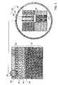
- FIG. 3an example silicon (Si) via etch in an example three-dimensional (3-D) wafer-to-wafer vertical stack 200 according to an embodiment of the present invention is illustrated.
- a tungsten “W” contact plug 310is formed during a standard W contact process.
- a nickel silicide (NiSi) etch stop layer 320is formed before the W contact plug 310 is established and before the wafers 210 and 220 are bonded.
- the Si via etchcan be stopped at the NiSi etch stop layer 320 to prevent etching through the W contact plug 310 .
- Each of the interwafer vias 224may contain an oxide layer 332 deposited on a sidewall, a copper (Cu) barrier/seed 334 deposited on the oxide layer 332 and the NiSi etch stop layer 320 , and copper (Cu) 336 electroplated on the Si via 224 to serve as an electrical connection between active IC devices located on the vertically stacked wafers 210 and 220 and an external interconnect.
- Cucopper
- Cucopper
- FIG. 4illustrates an example process of forming one or more silicon (Si) vias in an example three-dimensional (3-D) wafer-to-wafer vertical stack according to an embodiment of the present invention.
- interwafer vias 224are patterned by conventional lithography and the silicon (Si) is etched using an etch mask until stopped by the NiSi etch stop layer 320 at block 410 .
- an oxide layer 332as shown in FIG.
- a barrier/seed layer 334is then deposited on the oxide layer 332 and the bottom of the Si vias 224 at block 440 .
- copper (Cu)can then be deposited in the Si vias 224 , via electroplating and Chemical Mechanical Polish (CMP), to establish electrical connections between active IC devices located on the vertically stacked wafers 210 and 220 and an external interconnect, via the C4 bump 226 shown in FIG. 2 .
- CMPChemical Mechanical Polish
- the NiSi etch stop layercan effectively enable the silicon (Si) via etch to provide electrical conductivity between vertically stacked wafers without undesirable copper (Cu) oxidation or tungsten recess. If NiSi is already used as a silicide material in transistors of IC active devices, then no additional process steps may be required to form NiSi. The existing silicide material can be effectively used as an etch stop during the formation of one or more interwafer vias.
Landscapes
- Engineering & Computer Science (AREA)
- Microelectronics & Electronic Packaging (AREA)
- Power Engineering (AREA)
- Computer Hardware Design (AREA)
- Physics & Mathematics (AREA)
- Condensed Matter Physics & Semiconductors (AREA)
- General Physics & Mathematics (AREA)
- Manufacturing & Machinery (AREA)
- Plasma & Fusion (AREA)
- Chemical & Material Sciences (AREA)
- Chemical Kinetics & Catalysis (AREA)
- General Chemical & Material Sciences (AREA)
- Internal Circuitry In Semiconductor Integrated Circuit Devices (AREA)
Abstract
Description
This application is a continuation of and claims the benefit of application Ser. No. 10/443,831 filed May 23, 2003 now U.S. Pat. No. 7,148,565, which is a divisional of application Ser. No. 10/077,822, filed Feb. 20, 2002, which issued as U.S. Pat. No. 6,645,832 on Nov. 11, 2003, the contents of which are incorporated herein by reference in their entirety.
The present invention relates to a semiconductor process and, more specifically, relates to a method of using Nickel Silicide (NiSi) as an etch stop layer for the silicon (Si) via etch in vertically stacked wafer processing in a three-dimensional (3-D) wafer-to-wafer vertical stack.
Integrated circuits (ICs) form the basis for many electronic systems. Essentially, an integrated circuit (IC) includes a vast number of transistors and other circuit elements that are formed on a single semiconductor wafer or chip and are interconnected to implement a desired function. The complexity of these integrated circuits (ICs) requires the use of an ever increasing number of linked transistors and other circuit elements.
Many modern electronic systems are created through the use of a variety of different integrated circuits; each integrated circuit (IC) performing one or more specific functions. For example, computer systems include at least one microprocessor and a number of memory chips. Conventionally, each of these integrated circuits (ICs) is formed on a separate chip, packaged independently and interconnected on, for example, a printed circuit board (PCB).
As integrated circuit (IC) technology progresses, there is a growing desire for a “system on a chip” in which the functionality of all of the IC devices of the system are packaged together without a conventional PCB. Ideally, a computing system should be fabricated with all the necessary IC devices on a single chip. In practice, however, it is very difficult to implement a truly high-performance “system on a chip” because of vastly different fabrication processes and different manufacturing yields for the logic and memory circuits.
As a compromise, various “system modules” have been introduced that electrically connect and package integrated circuit (IC) devices which are fabricated on the same or on different semiconductor wafers. Initially, system modules have been created by simply stacking two chips, e.g., a logic and memory chip, one on top of the other in an arrangement commonly referred to as chip-on-chip structure. Subsequently, multi-chip module (MCM) technology has been utilized to stack a number of chips on a common substrate to reduce the overall size and weight of the package, which directly translates into reduced system size.
Existing multi-chip module (MCM) technology is known to provide performance enhancements over single chip or chip-on-chip (COC) packaging approaches. For example, when several semiconductor chips are mounted and interconnected on a common substrate through very high density interconnects, higher silicon packaging density and shorter chip-to-chip interconnections can be achieved. In addition, low dielectric constant materials and higher wiring density can also be obtained which lead to the increased system speed and reliability, and the reduced weight, volume, power consumption and heat to be dissipated for the same level of performance. However, MCM approaches still suffer from additional problems, such as bulky package, wire length and wire bonding that gives rise to stray inductances that interfere with the operation of the system module.
An advanced three-dimensional (3D) wafer-to-wafer vertical stack technology has been recently proposed by researchers to realize the ideal high-performance “system on a chip”. In contrast to the existing multi-chip module (MCM) technology which seeks to stack multiple chips on a common substrate, 3-D wafer-to-wafer vertical stack technology seeks to achieve the long-awaited goal of vertically stacking many layers of active IC devices such as processors, programmable devices and memory devices inside a single chip to shorten average wire lengths, thereby reducing interconnect RC delay and increasing system performance.
One major challenge of 3-D wafer-to-wafer vertical stack integration technology is the bonding between wafers and between die in a single chip. In general, a dielectric layer is used to bond respective wafers. In the dielectric bonding method, high aspect ratio silicon (Si) via etch is required to provide electrical conductivity between vertically stacked wafers. Therefore, a metal bonding method is preferred to stack wafers. However, existing etch stop layers for silicon (Si) via etch in wafer stacking with metal bonding method can cause oxidation or metal recess which may negatively impact the power delivery system. Therefore, a need exists for an improved etch stop layer for the Si via etch in vertically stacked wafer processing (i.e., 3-D interconnect processing) which provides electrical conductivity between vertically stacked wafers.
A more complete appreciation of exemplary embodiments of the present invention, and many of the attendant advantages of the present invention, will become readily apparent as the same becomes better understood by reference to the following detailed description when considered in conjunction with the accompanying drawings in which like reference symbols indicate the same or similar components, wherein:
The present invention is applicable for use with all types of semiconductor wafers and integrated circuit (IC) devices, including, for example, MOS transistors, CMOS devices, MOSFETs, and new memory devices and communication devices such as smart card, cellular phone, electronic tags, gaming devices which may become available as semiconductor technology develops in the future. However, for the sake of simplicity, discussions will concentrate mainly on exemplary use of a simple three-dimensional (3-D) wafer-to-wafer vertical stack and an etch stop layer for metallic wafer-to-wafer and die-to-die bonding in such a three-dimensional (3-D) wafer-to-wafer vertical stack, although the scope of the present invention is not limited thereto.
Attention now is directed to the drawings and particularly toFIG. 1 , an example three-dimensional (3-D) wafer-to-wafer vertical stack is illustrated. As shown inFIG. 1 , the 3-D vertical stack (chip)100 may comprise any number of active device polysilicon (Si) wafers, such as wafer #1110 including, for example, one or more microprocessors; wafer #2120 including one or more memory devices; and wafer #3130 including one or more radio-frequency (RF) or optical communication devices. Thebottom wafer 110 is typically thick to support the stacking of thetop wafers top wafers wafers
In a typical 3-Dvertical stack 100 shown inFIG. 1 , the active device wafers110,120 and130 are bonded using adielectric layer 102, while all active layers onwafers dielectric layer 102 can be cost-prohibitive for mass production. In addition, the interwafer vias104 betweenadjacent wafers
As a result, a metal to metal bond can be used to stackwafers vertical stack 100 shown inFIG. 1 . This metal to metal bond method can serve not only as electrical connections to active IC devices on the verticallystacked wafers vertical stack 100 but also bondadjacent wafers stacked wafers
Turning now toFIG. 2 , an example three-dimensional (3-D) wafer-to-wafer vertical stack according to an embodiment of the present invention is illustrated. Specifically,FIG. 2 illustrates an example 2-wafervertical stack 200 according to an embodiment of the present invention. However, the number of wafers in a vertical stack is not limited thereto. Through 3-D interconnect structure, wiring between vertically stacked wafers can be shortened resulting in a faster signal and minimal interconnect RC delays. In addition, the vertical stack can effectively integrate diverse process technologies on a single wafer process, such as, for example, logic/memory stacking, processor stacking, optical interconnect, system-on-chip, and RF interconnect.
As shown inFIG. 2 , the bottom silicon (Si)wafer 210 contains anactive device layer 212 supporting one or more active IC devices (not shown). Likewise, thetop Si wafer 220 also contains anactive device layer 222 supporting one or more active IC devices (not shown). Thewafers metal bonding layer 106 deposited on opposing surfaces of thebottom wafer 210 and thetop wafer 220 at designated bonding areas to establish electrical connections between active IC devices on verticallystacked wafers adjacent wafers ILD layer 108. Thetop wafer 220 can also be thinned by either a Chemical Mechanical Polish (CMP), grinding, or Silicon (Si) wet etch process so as to be much more pliable than those of standard thickness and to allow for greater thickness variations across the verticallystacked wafers
In the example 2-wafervertical stack 200 shown inFIG. 2 , the metal bonding process betweenadjacent wafers adjacent wafers adjacent wafers metal bonding layer 106 may include a plurality of Copper (Cu) lines on opposing surfaces of the verticallystacked wafers stacked wafers
After the wafer bonding and silicon (Si) thinning processes are completed, one ormore interwafer vias 224 may be etched, via thetop wafer 220, to establish electrical connections of active IC devices between vertically stackedwafers C4 bump 226. Typically a tungsten “W” plug (metal contact layer) is formed during a standard W contact process to establish an interconnect with the copper (Cu) lines (the metal bonding layer106) of the vertically stackedwafers wafers wafers
Turning now toFIG. 3 , an example silicon (Si) via etch in an example three-dimensional (3-D) wafer-to-wafervertical stack 200 according to an embodiment of the present invention is illustrated. As shown inFIG. 3 , a tungsten “W”contact plug 310 is formed during a standard W contact process. A nickel silicide (NiSi)etch stop layer 320 is formed before theW contact plug 310 is established and before thewafers etch stop layer 320 to prevent etching through theW contact plug 310. Each of the interwafer vias224 may contain anoxide layer 332 deposited on a sidewall, a copper (Cu) barrier/seed 334 deposited on theoxide layer 332 and the NiSietch stop layer 320, and copper (Cu)336 electroplated on the Si via224 to serve as an electrical connection between active IC devices located on the vertically stackedwafers
As described in this invention, the NiSi etch stop layer according to an embodiment of the present invention can effectively enable the silicon (Si) via etch to provide electrical conductivity between vertically stacked wafers without undesirable copper (Cu) oxidation or tungsten recess. If NiSi is already used as a silicide material in transistors of IC active devices, then no additional process steps may be required to form NiSi. The existing silicide material can be effectively used as an etch stop during the formation of one or more interwafer vias.
While there have been illustrated and described what are considered to be exemplary embodiments of the present invention, it will be understood by those skilled in the art and as technology develops that various changes and modifications may be made, and equivalents may be substituted for elements thereof without departing from the true scope of the present invention. For example, other types of metallic materials that exhibit a high selectivity with the silicon (Si) via etch may also be used in lieu of NiSi (Nickel Silicide) to serve as an etch stop layer. Many modifications may be made to adapt the teachings of the present invention to a particular situation without departing from the scope thereof. Therefore, it is intended that the present invention not be limited to the various exemplary embodiments disclosed, but that the present invention includes all embodiments falling within the scope of the appended claims.
Claims (20)
1. A method of forming a silicon (Si) via in vertically stacked wafers having a contact plug extending from selected metallic lines of a top wafer and an etch stop layer processed before the contact plug, comprising:
selectively etching a silicon (Si) layer of the top wafer until stopped by an etch stop layer comprised of a material selective to a silicon etch to form a Si via;
depositing an oxide layer to insulate a sidewall of the Si via;
forming a barrier/seed layer on the Si via; and
filling the Si via with a conduction metal to provide electrical connection between active IC devices located on the vertically stacked wafers and an external interconnect.
2. The method as claimed inclaim 1 , wherein the contact plug is comprised of tungsten (W).
3. The method as claimed inclaim 1 , wherein the vertically stacked wafers are bonded via respective metallic lines which serve as electrical contacts between active IC devices on the vertically stacked wafers.
4. A method, comprising:
forming an etch stop layer comprised of a material selective to a silicon etch on designated areas on a surface of a top wafer;
forming a contact plug layer on the etch stop layer on the designated areas on the surface of the top wafer;
forming vertically stacked wafers by bonding the top wafer with a bottom wafer, via respective metallic lines; and
forming an interwafer via on the top wafer by selectively etching through a silicon (Si) layer of the top wafer until stopped by the etch stop layer comprised of the material selective to the silicon etch, depositing an oxide layer to insulate a sidewall of the interwafer via, depositing a barrier/seed layer on the oxide layer and on the bottom of the interwafer via, and filling the interwafer via with a conduction metal to provide electrical connection between active IC devices located on the vertically stacked wafers and an external interconnect.
5. The method as claimed inclaim 4 , wherein the respective metallic lines are copper (Cu) lines deposited on opposing surfaces of the vertically stacked wafers to serve as electrical contacts between the active IC devices located on the vertically stacked wafers.
6. The method as claimed inclaim 4 , wherein the conduction metal deposited in the Si via is comprised of copper (Cu).
7. The method as claimed inclaim 4 , further comprising: thinning the top wafer so that the top wafer is thinner than the bottom wafer.
8. The method as claimed inclaim 7 , wherein forming an etch stop layer comprised of the material selective to the silicon etch comprises forming an etch stop layer comprised of nickel silicide (NiSi).
9. A method of forming a vertically stacked wafer structure, comprising:
providing a top wafer including an active layer and a dielectric layer, the active layer comprised of silicon;
forming an interconnect in the dielectric layer, wherein forming the interconnect comprises:
forming an etch stop layer at an end of the interconnect, the etch stop layer contacting the active layer and comprised of a material selective to a silicon etch;
providing a contact plug in contact with the etch stop layer;
forming a first metal line in contact with the contact plug;
forming a second metal line on a corresponding surface of a bottom wafer;
bonding the first metal line and the second metal line to establish metal bonding between the top wafer and the bottom wafer;
etching the active layer of the top wafer until stopped by the etch stop layer to form a Si via;
depositing an oxide layer to insulate a sidewall of the Si via; and
filling the Si via with a conduction metal to provide electrical connection between active IC devices located on the wafers and an external interconnect.
10. The method as claimed inclaim 9 , wherein providing the contact plug comprises providing a contact plug comprised of tungsten (W).
11. The method as claimed inclaim 9 , wherein the material selective to the silicon etch is NiSi.
12. The method as claimed inclaim 9 , further comprising:
prior to etching the active layer to form the Si via, thinning the top wafer by one of: Chemical Mechanical Polish (CMP), grinding, or a Si wet etch process.
13. The method as claimed inclaim 9 , further comprising:
subsequent to depositing the oxide layer and prior to filling the Si via with the conduction metal, forming a baffler/seed layer on the Si via.
14. The method as claimed inclaim 13 , wherein forming the baffler/seed layer on the Si via comprises depositing a copper (Cu) barrier/seed layer on the oxide layer and the etch stop layer.
15. The method as claimed inclaim 9 , wherein filling the Si via with the conduction metal comprises electroplating the Si via with copper (Cu).
16. The method as claimed inclaim 9 , wherein forming the first metal line in contact with the contact plug comprises forming a copper (Cu) metal line in contact with the contact plug.
17. The method as claimed inclaim 9 , wherein forming the first metal line in contact with the contact plug comprises forming a first metal line comprised of a material selected from the group consisting of: tin, indium, gold, nickel, silver, palladium, palladium-nickel alloy, and titanium.
18. The method as claimed inclaim 9 , further comprising:
providing a dummy metal bonding pad between the top wafer and the bottom wafer.
19. The method as claimed inclaim 9 , further comprising:
forming the external interconnect on the Si via.
20. The method as claimed inclaim 9 , wherein the active layer of the top wafer includes active devices associated with a first system, and the bottom wafer includes active devices associated with a second system, the systems differing and each system selected from the group consisting of: a logic system, a memory system, and a communications system.
Priority Applications (1)
| Application Number | Priority Date | Filing Date | Title |
|---|---|---|---|
| US11/528,986US7615462B2 (en) | 2002-02-20 | 2006-09-27 | Etch stop layer for silicon (Si) via etch in three-dimensional (3-D) wafer-to-wafer vertical stack |
Applications Claiming Priority (3)
| Application Number | Priority Date | Filing Date | Title |
|---|---|---|---|
| US10/077,822US6645832B2 (en) | 2002-02-20 | 2002-02-20 | Etch stop layer for silicon (Si) via etch in three-dimensional (3-D) wafer-to-wafer vertical stack |
| US10/443,831US7148565B2 (en) | 2002-02-20 | 2003-05-23 | Etch stop layer for silicon (Si) via etch in three-dimensional (3-D) wafer-to-wafer vertical stack |
| US11/528,986US7615462B2 (en) | 2002-02-20 | 2006-09-27 | Etch stop layer for silicon (Si) via etch in three-dimensional (3-D) wafer-to-wafer vertical stack |
Related Parent Applications (1)
| Application Number | Title | Priority Date | Filing Date |
|---|---|---|---|
| US10/443,831ContinuationUS7148565B2 (en) | 2002-02-20 | 2003-05-23 | Etch stop layer for silicon (Si) via etch in three-dimensional (3-D) wafer-to-wafer vertical stack |
Publications (2)
| Publication Number | Publication Date |
|---|---|
| US20070020805A1 US20070020805A1 (en) | 2007-01-25 |
| US7615462B2true US7615462B2 (en) | 2009-11-10 |
Family
ID=27732725
Family Applications (3)
| Application Number | Title | Priority Date | Filing Date |
|---|---|---|---|
| US10/077,822Expired - LifetimeUS6645832B2 (en) | 2002-02-20 | 2002-02-20 | Etch stop layer for silicon (Si) via etch in three-dimensional (3-D) wafer-to-wafer vertical stack |
| US10/443,831Expired - LifetimeUS7148565B2 (en) | 2002-02-20 | 2003-05-23 | Etch stop layer for silicon (Si) via etch in three-dimensional (3-D) wafer-to-wafer vertical stack |
| US11/528,986Expired - Fee RelatedUS7615462B2 (en) | 2002-02-20 | 2006-09-27 | Etch stop layer for silicon (Si) via etch in three-dimensional (3-D) wafer-to-wafer vertical stack |
Family Applications Before (2)
| Application Number | Title | Priority Date | Filing Date |
|---|---|---|---|
| US10/077,822Expired - LifetimeUS6645832B2 (en) | 2002-02-20 | 2002-02-20 | Etch stop layer for silicon (Si) via etch in three-dimensional (3-D) wafer-to-wafer vertical stack |
| US10/443,831Expired - LifetimeUS7148565B2 (en) | 2002-02-20 | 2003-05-23 | Etch stop layer for silicon (Si) via etch in three-dimensional (3-D) wafer-to-wafer vertical stack |
Country Status (1)
| Country | Link |
|---|---|
| US (3) | US6645832B2 (en) |
Cited By (147)
| Publication number | Priority date | Publication date | Assignee | Title |
|---|---|---|---|---|
| US8492260B2 (en) | 2010-08-30 | 2013-07-23 | Semionductor Components Industries, LLC | Processes of forming an electronic device including a feature in a trench |
| US8981533B2 (en) | 2012-09-13 | 2015-03-17 | Semiconductor Components Industries, Llc | Electronic device including a via and a conductive structure, a process of forming the same, and an interposer |
| US9812354B2 (en) | 2015-05-15 | 2017-11-07 | Semiconductor Components Industries, Llc | Process of forming an electronic device including a material defining a void |
| US10825779B2 (en) | 2015-04-19 | 2020-11-03 | Monolithic 3D Inc. | 3D semiconductor device and structure |
| US10833108B2 (en) | 2010-10-13 | 2020-11-10 | Monolithic 3D Inc. | 3D microdisplay device and structure |
| US10840239B2 (en) | 2014-08-26 | 2020-11-17 | Monolithic 3D Inc. | 3D semiconductor device and structure |
| US10847540B2 (en) | 2015-10-24 | 2020-11-24 | Monolithic 3D Inc. | 3D semiconductor memory device and structure |
| US10892016B1 (en) | 2019-04-08 | 2021-01-12 | Monolithic 3D Inc. | 3D memory semiconductor devices and structures |
| US10896931B1 (en) | 2010-10-11 | 2021-01-19 | Monolithic 3D Inc. | 3D semiconductor device and structure |
| US10903089B1 (en) | 2012-12-29 | 2021-01-26 | Monolithic 3D Inc. | 3D semiconductor device and structure |
| US10910364B2 (en) | 2009-10-12 | 2021-02-02 | Monolitaic 3D Inc. | 3D semiconductor device |
| US10943934B2 (en) | 2010-10-13 | 2021-03-09 | Monolithic 3D Inc. | Multilevel semiconductor device and structure |
| US10978501B1 (en) | 2010-10-13 | 2021-04-13 | Monolithic 3D Inc. | Multilevel semiconductor device and structure with waveguides |
| US10998374B1 (en) | 2010-10-13 | 2021-05-04 | Monolithic 3D Inc. | Multilevel semiconductor device and structure |
| US11004967B1 (en) | 2013-03-11 | 2021-05-11 | Monolithic 3D Inc. | 3D semiconductor device and structure with memory |
| US11004719B1 (en) | 2010-11-18 | 2021-05-11 | Monolithic 3D Inc. | Methods for producing a 3D semiconductor memory device and structure |
| US11004694B1 (en) | 2012-12-29 | 2021-05-11 | Monolithic 3D Inc. | 3D semiconductor device and structure |
| US11011507B1 (en) | 2015-04-19 | 2021-05-18 | Monolithic 3D Inc. | 3D semiconductor device and structure |
| US11018133B2 (en) | 2009-10-12 | 2021-05-25 | Monolithic 3D Inc. | 3D integrated circuit |
| US11018191B1 (en) | 2010-10-11 | 2021-05-25 | Monolithic 3D Inc. | 3D semiconductor device and structure |
| US11018042B1 (en) | 2010-11-18 | 2021-05-25 | Monolithic 3D Inc. | 3D semiconductor memory device and structure |
| US11018116B2 (en) | 2012-12-22 | 2021-05-25 | Monolithic 3D Inc. | Method to form a 3D semiconductor device and structure |
| US11018156B2 (en) | 2019-04-08 | 2021-05-25 | Monolithic 3D Inc. | 3D memory semiconductor devices and structures |
| US11024673B1 (en) | 2010-10-11 | 2021-06-01 | Monolithic 3D Inc. | 3D semiconductor device and structure |
| US11031394B1 (en) | 2014-01-28 | 2021-06-08 | Monolithic 3D Inc. | 3D semiconductor device and structure |
| US11031275B2 (en) | 2010-11-18 | 2021-06-08 | Monolithic 3D Inc. | 3D semiconductor device and structure with memory |
| US11043523B1 (en) | 2010-10-13 | 2021-06-22 | Monolithic 3D Inc. | Multilevel semiconductor device and structure with image sensors |
| US11056468B1 (en) | 2015-04-19 | 2021-07-06 | Monolithic 3D Inc. | 3D semiconductor device and structure |
| US11063071B1 (en) | 2010-10-13 | 2021-07-13 | Monolithic 3D Inc. | Multilevel semiconductor device and structure with waveguides |
| US11063024B1 (en) | 2012-12-22 | 2021-07-13 | Monlithic 3D Inc. | Method to form a 3D semiconductor device and structure |
| US11087995B1 (en) | 2012-12-29 | 2021-08-10 | Monolithic 3D Inc. | 3D semiconductor device and structure |
| US11088130B2 (en) | 2014-01-28 | 2021-08-10 | Monolithic 3D Inc. | 3D semiconductor device and structure |
| US11088050B2 (en) | 2012-04-09 | 2021-08-10 | Monolithic 3D Inc. | 3D semiconductor device with isolation layers |
| US11094576B1 (en) | 2010-11-18 | 2021-08-17 | Monolithic 3D Inc. | Methods for producing a 3D semiconductor memory device and structure |
| US11107808B1 (en) | 2014-01-28 | 2021-08-31 | Monolithic 3D Inc. | 3D semiconductor device and structure |
| US11107721B2 (en) | 2010-11-18 | 2021-08-31 | Monolithic 3D Inc. | 3D semiconductor device and structure with NAND logic |
| US11114464B2 (en) | 2015-10-24 | 2021-09-07 | Monolithic 3D Inc. | 3D semiconductor device and structure |
| US11114427B2 (en) | 2015-11-07 | 2021-09-07 | Monolithic 3D Inc. | 3D semiconductor processor and memory device and structure |
| US11133344B2 (en) | 2010-10-13 | 2021-09-28 | Monolithic 3D Inc. | Multilevel semiconductor device and structure with image sensors |
| US11158674B2 (en) | 2010-10-11 | 2021-10-26 | Monolithic 3D Inc. | Method to produce a 3D semiconductor device and structure |
| US11158652B1 (en) | 2019-04-08 | 2021-10-26 | Monolithic 3D Inc. | 3D memory semiconductor devices and structures |
| US11163112B2 (en) | 2010-10-13 | 2021-11-02 | Monolithic 3D Inc. | Multilevel semiconductor device and structure with electromagnetic modulators |
| US11164770B1 (en) | 2010-11-18 | 2021-11-02 | Monolithic 3D Inc. | Method for producing a 3D semiconductor memory device and structure |
| US11164898B2 (en) | 2010-10-13 | 2021-11-02 | Monolithic 3D Inc. | Multilevel semiconductor device and structure |
| US11164811B2 (en) | 2012-04-09 | 2021-11-02 | Monolithic 3D Inc. | 3D semiconductor device with isolation layers and oxide-to-oxide bonding |
| US11177140B2 (en) | 2012-12-29 | 2021-11-16 | Monolithic 3D Inc. | 3D semiconductor device and structure |
| US11211279B2 (en) | 2010-11-18 | 2021-12-28 | Monolithic 3D Inc. | Method for processing a 3D integrated circuit and structure |
| US11217565B2 (en) | 2012-12-22 | 2022-01-04 | Monolithic 3D Inc. | Method to form a 3D semiconductor device and structure |
| US11227897B2 (en) | 2010-10-11 | 2022-01-18 | Monolithic 3D Inc. | Method for producing a 3D semiconductor memory device and structure |
| US11251149B2 (en) | 2016-10-10 | 2022-02-15 | Monolithic 3D Inc. | 3D memory device and structure |
| US11257867B1 (en) | 2010-10-11 | 2022-02-22 | Monolithic 3D Inc. | 3D semiconductor device and structure with oxide bonds |
| US11270055B1 (en) | 2013-04-15 | 2022-03-08 | Monolithic 3D Inc. | Automation for monolithic 3D devices |
| US11296106B2 (en) | 2019-04-08 | 2022-04-05 | Monolithic 3D Inc. | 3D memory semiconductor devices and structures |
| US11296115B1 (en) | 2015-10-24 | 2022-04-05 | Monolithic 3D Inc. | 3D semiconductor device and structure |
| US11309292B2 (en) | 2012-12-22 | 2022-04-19 | Monolithic 3D Inc. | 3D semiconductor device and structure with metal layers |
| US11315980B1 (en) | 2010-10-11 | 2022-04-26 | Monolithic 3D Inc. | 3D semiconductor device and structure with transistors |
| US11327227B2 (en) | 2010-10-13 | 2022-05-10 | Monolithic 3D Inc. | Multilevel semiconductor device and structure with electromagnetic modulators |
| US11329059B1 (en) | 2016-10-10 | 2022-05-10 | Monolithic 3D Inc. | 3D memory devices and structures with thinned single crystal substrates |
| US11341309B1 (en) | 2013-04-15 | 2022-05-24 | Monolithic 3D Inc. | Automation for monolithic 3D devices |
| US11355380B2 (en) | 2010-11-18 | 2022-06-07 | Monolithic 3D Inc. | Methods for producing 3D semiconductor memory device and structure utilizing alignment marks |
| US11355381B2 (en) | 2010-11-18 | 2022-06-07 | Monolithic 3D Inc. | 3D semiconductor memory device and structure |
| US11374118B2 (en) | 2009-10-12 | 2022-06-28 | Monolithic 3D Inc. | Method to form a 3D integrated circuit |
| US11398569B2 (en) | 2013-03-12 | 2022-07-26 | Monolithic 3D Inc. | 3D semiconductor device and structure |
| US11404466B2 (en) | 2010-10-13 | 2022-08-02 | Monolithic 3D Inc. | Multilevel semiconductor device and structure with image sensors |
| US11410912B2 (en) | 2012-04-09 | 2022-08-09 | Monolithic 3D Inc. | 3D semiconductor device with vias and isolation layers |
| US11430667B2 (en) | 2012-12-29 | 2022-08-30 | Monolithic 3D Inc. | 3D semiconductor device and structure with bonding |
| US11430668B2 (en) | 2012-12-29 | 2022-08-30 | Monolithic 3D Inc. | 3D semiconductor device and structure with bonding |
| US11437368B2 (en) | 2010-10-13 | 2022-09-06 | Monolithic 3D Inc. | Multilevel semiconductor device and structure with oxide bonding |
| US11443971B2 (en) | 2010-11-18 | 2022-09-13 | Monolithic 3D Inc. | 3D semiconductor device and structure with memory |
| US11469271B2 (en) | 2010-10-11 | 2022-10-11 | Monolithic 3D Inc. | Method to produce 3D semiconductor devices and structures with memory |
| US11476181B1 (en) | 2012-04-09 | 2022-10-18 | Monolithic 3D Inc. | 3D semiconductor device and structure with metal layers |
| US11482438B2 (en) | 2010-11-18 | 2022-10-25 | Monolithic 3D Inc. | Methods for producing a 3D semiconductor memory device and structure |
| US11482440B2 (en) | 2010-12-16 | 2022-10-25 | Monolithic 3D Inc. | 3D semiconductor device and structure with a built-in test circuit for repairing faulty circuits |
| US11482439B2 (en) | 2010-11-18 | 2022-10-25 | Monolithic 3D Inc. | Methods for producing a 3D semiconductor memory device comprising charge trap junction-less transistors |
| US11487928B2 (en) | 2013-04-15 | 2022-11-01 | Monolithic 3D Inc. | Automation for monolithic 3D devices |
| US11495484B2 (en) | 2010-11-18 | 2022-11-08 | Monolithic 3D Inc. | 3D semiconductor devices and structures with at least two single-crystal layers |
| US11508605B2 (en) | 2010-11-18 | 2022-11-22 | Monolithic 3D Inc. | 3D semiconductor memory device and structure |
| US11521888B2 (en) | 2010-11-18 | 2022-12-06 | Monolithic 3D Inc. | 3D semiconductor device and structure with high-k metal gate transistors |
| US11569117B2 (en) | 2010-11-18 | 2023-01-31 | Monolithic 3D Inc. | 3D semiconductor device and structure with single-crystal layers |
| US11574109B1 (en) | 2013-04-15 | 2023-02-07 | Monolithic 3D Inc | Automation methods for 3D integrated circuits and devices |
| US11594473B2 (en) | 2012-04-09 | 2023-02-28 | Monolithic 3D Inc. | 3D semiconductor device and structure with metal layers and a connective path |
| US11600667B1 (en) | 2010-10-11 | 2023-03-07 | Monolithic 3D Inc. | Method to produce 3D semiconductor devices and structures with memory |
| US11605663B2 (en) | 2010-10-13 | 2023-03-14 | Monolithic 3D Inc. | Multilevel semiconductor device and structure with image sensors and wafer bonding |
| US11610802B2 (en) | 2010-11-18 | 2023-03-21 | Monolithic 3D Inc. | Method for producing a 3D semiconductor device and structure with single crystal transistors and metal gate electrodes |
| US11616004B1 (en) | 2012-04-09 | 2023-03-28 | Monolithic 3D Inc. | 3D semiconductor device and structure with metal layers and a connective path |
| US11615977B2 (en) | 2010-11-18 | 2023-03-28 | Monolithic 3D Inc. | 3D semiconductor memory device and structure |
| US11694922B2 (en) | 2010-10-13 | 2023-07-04 | Monolithic 3D Inc. | Multilevel semiconductor device and structure with oxide bonding |
| US11694944B1 (en) | 2012-04-09 | 2023-07-04 | Monolithic 3D Inc. | 3D semiconductor device and structure with metal layers and a connective path |
| US11711928B2 (en) | 2016-10-10 | 2023-07-25 | Monolithic 3D Inc. | 3D memory devices and structures with control circuits |
| US11720736B2 (en) | 2013-04-15 | 2023-08-08 | Monolithic 3D Inc. | Automation methods for 3D integrated circuits and devices |
| US11735501B1 (en) | 2012-04-09 | 2023-08-22 | Monolithic 3D Inc. | 3D semiconductor device and structure with metal layers and a connective path |
| US11735462B2 (en) | 2010-11-18 | 2023-08-22 | Monolithic 3D Inc. | 3D semiconductor device and structure with single-crystal layers |
| US11763864B2 (en) | 2019-04-08 | 2023-09-19 | Monolithic 3D Inc. | 3D memory semiconductor devices and structures with bit-line pillars |
| US11784169B2 (en) | 2012-12-22 | 2023-10-10 | Monolithic 3D Inc. | 3D semiconductor device and structure with metal layers |
| US11784082B2 (en) | 2010-11-18 | 2023-10-10 | Monolithic 3D Inc. | 3D semiconductor device and structure with bonding |
| US11804396B2 (en) | 2010-11-18 | 2023-10-31 | Monolithic 3D Inc. | Methods for producing a 3D semiconductor device and structure with memory cells and multiple metal layers |
| US11812620B2 (en) | 2016-10-10 | 2023-11-07 | Monolithic 3D Inc. | 3D DRAM memory devices and structures with control circuits |
| US11855100B2 (en) | 2010-10-13 | 2023-12-26 | Monolithic 3D Inc. | Multilevel semiconductor device and structure with oxide bonding |
| US11855114B2 (en) | 2010-10-13 | 2023-12-26 | Monolithic 3D Inc. | Multilevel semiconductor device and structure with image sensors and wafer bonding |
| US11854857B1 (en) | 2010-11-18 | 2023-12-26 | Monolithic 3D Inc. | Methods for producing a 3D semiconductor device and structure with memory cells and multiple metal layers |
| US11862503B2 (en) | 2010-11-18 | 2024-01-02 | Monolithic 3D Inc. | Method for producing a 3D semiconductor device and structure with memory cells and multiple metal layers |
| US11869965B2 (en) | 2013-03-11 | 2024-01-09 | Monolithic 3D Inc. | 3D semiconductor device and structure with metal layers and memory cells |
| US11869915B2 (en) | 2010-10-13 | 2024-01-09 | Monolithic 3D Inc. | Multilevel semiconductor device and structure with image sensors and wafer bonding |
| US11869591B2 (en) | 2016-10-10 | 2024-01-09 | Monolithic 3D Inc. | 3D memory devices and structures with control circuits |
| US11881443B2 (en) | 2012-04-09 | 2024-01-23 | Monolithic 3D Inc. | 3D semiconductor device and structure with metal layers and a connective path |
| US11901210B2 (en) | 2010-11-18 | 2024-02-13 | Monolithic 3D Inc. | 3D semiconductor device and structure with memory |
| US11916045B2 (en) | 2012-12-22 | 2024-02-27 | Monolithic 3D Inc. | 3D semiconductor device and structure with metal layers |
| US11923230B1 (en) | 2010-11-18 | 2024-03-05 | Monolithic 3D Inc. | 3D semiconductor device and structure with bonding |
| US11923374B2 (en) | 2013-03-12 | 2024-03-05 | Monolithic 3D Inc. | 3D semiconductor device and structure with metal layers |
| US11929372B2 (en) | 2010-10-13 | 2024-03-12 | Monolithic 3D Inc. | Multilevel semiconductor device and structure with image sensors and wafer bonding |
| US11930648B1 (en) | 2016-10-10 | 2024-03-12 | Monolithic 3D Inc. | 3D memory devices and structures with metal layers |
| US11937422B2 (en) | 2015-11-07 | 2024-03-19 | Monolithic 3D Inc. | Semiconductor memory device and structure |
| US11935949B1 (en) | 2013-03-11 | 2024-03-19 | Monolithic 3D Inc. | 3D semiconductor device and structure with metal layers and memory cells |
| US11956952B2 (en) | 2015-08-23 | 2024-04-09 | Monolithic 3D Inc. | Semiconductor memory device and structure |
| US11961827B1 (en) | 2012-12-22 | 2024-04-16 | Monolithic 3D Inc. | 3D semiconductor device and structure with metal layers |
| US11967583B2 (en) | 2012-12-22 | 2024-04-23 | Monolithic 3D Inc. | 3D semiconductor device and structure with metal layers |
| US11978731B2 (en) | 2015-09-21 | 2024-05-07 | Monolithic 3D Inc. | Method to produce a multi-level semiconductor memory device and structure |
| US11984438B2 (en) | 2010-10-13 | 2024-05-14 | Monolithic 3D Inc. | Multilevel semiconductor device and structure with oxide bonding |
| US11984445B2 (en) | 2009-10-12 | 2024-05-14 | Monolithic 3D Inc. | 3D semiconductor devices and structures with metal layers |
| US11991884B1 (en) | 2015-10-24 | 2024-05-21 | Monolithic 3D Inc. | 3D semiconductor device and structure with logic and memory |
| US12016181B2 (en) | 2015-10-24 | 2024-06-18 | Monolithic 3D Inc. | 3D semiconductor device and structure with logic and memory |
| US12027518B1 (en) | 2009-10-12 | 2024-07-02 | Monolithic 3D Inc. | 3D semiconductor devices and structures with metal layers |
| US12035531B2 (en) | 2015-10-24 | 2024-07-09 | Monolithic 3D Inc. | 3D semiconductor device and structure with logic and memory |
| US12033884B2 (en) | 2010-11-18 | 2024-07-09 | Monolithic 3D Inc. | Methods for producing a 3D semiconductor device and structure with memory cells and multiple metal layers |
| US12051674B2 (en) | 2012-12-22 | 2024-07-30 | Monolithic 3D Inc. | 3D semiconductor device and structure with metal layers |
| US12068187B2 (en) | 2010-11-18 | 2024-08-20 | Monolithic 3D Inc. | 3D semiconductor device and structure with bonding and DRAM memory cells |
| US12080743B2 (en) | 2010-10-13 | 2024-09-03 | Monolithic 3D Inc. | Multilevel semiconductor device and structure with image sensors and wafer bonding |
| US12094892B2 (en) | 2010-10-13 | 2024-09-17 | Monolithic 3D Inc. | 3D micro display device and structure |
| US12094965B2 (en) | 2013-03-11 | 2024-09-17 | Monolithic 3D Inc. | 3D semiconductor device and structure with metal layers and memory cells |
| US12094829B2 (en) | 2014-01-28 | 2024-09-17 | Monolithic 3D Inc. | 3D semiconductor device and structure |
| US12100646B2 (en) | 2013-03-12 | 2024-09-24 | Monolithic 3D Inc. | 3D semiconductor device and structure with metal layers |
| US12100658B2 (en) | 2015-09-21 | 2024-09-24 | Monolithic 3D Inc. | Method to produce a 3D multilayer semiconductor device and structure |
| US12100611B2 (en) | 2010-11-18 | 2024-09-24 | Monolithic 3D Inc. | Methods for producing a 3D semiconductor device and structure with memory cells and multiple metal layers |
| US12120880B1 (en) | 2015-10-24 | 2024-10-15 | Monolithic 3D Inc. | 3D semiconductor device and structure with logic and memory |
| US12125737B1 (en) | 2010-11-18 | 2024-10-22 | Monolithic 3D Inc. | 3D semiconductor device and structure with metal layers and memory cells |
| US12136562B2 (en) | 2010-11-18 | 2024-11-05 | Monolithic 3D Inc. | 3D semiconductor device and structure with single-crystal layers |
| US12144190B2 (en) | 2010-11-18 | 2024-11-12 | Monolithic 3D Inc. | 3D semiconductor device and structure with bonding and memory cells preliminary class |
| US12154817B1 (en) | 2010-11-18 | 2024-11-26 | Monolithic 3D Inc. | Methods for producing a 3D semiconductor memory device and structure |
| US12178055B2 (en) | 2015-09-21 | 2024-12-24 | Monolithic 3D Inc. | 3D semiconductor memory devices and structures |
| US12219769B2 (en) | 2015-10-24 | 2025-02-04 | Monolithic 3D Inc. | 3D semiconductor device and structure with logic and memory |
| US12225704B2 (en) | 2016-10-10 | 2025-02-11 | Monolithic 3D Inc. | 3D memory devices and structures with memory arrays and metal layers |
| US12243765B2 (en) | 2010-11-18 | 2025-03-04 | Monolithic 3D Inc. | 3D semiconductor device and structure with metal layers and memory cells |
| US12250830B2 (en) | 2015-09-21 | 2025-03-11 | Monolithic 3D Inc. | 3D semiconductor memory devices and structures |
| US12249538B2 (en) | 2012-12-29 | 2025-03-11 | Monolithic 3D Inc. | 3D semiconductor device and structure including power distribution grids |
| US12272586B2 (en) | 2010-11-18 | 2025-04-08 | Monolithic 3D Inc. | 3D semiconductor memory device and structure with memory and metal layers |
| US12362219B2 (en) | 2010-11-18 | 2025-07-15 | Monolithic 3D Inc. | 3D semiconductor memory device and structure |
| US12360310B2 (en) | 2010-10-13 | 2025-07-15 | Monolithic 3D Inc. | Multilevel semiconductor device and structure with oxide bonding |
Families Citing this family (74)
| Publication number | Priority date | Publication date | Assignee | Title |
|---|---|---|---|---|
| US7805756B2 (en) | 1996-11-29 | 2010-09-28 | Frampton E Ellis | Microchips with inner firewalls, faraday cages, and/or photovoltaic cells |
| US20050180095A1 (en) | 1996-11-29 | 2005-08-18 | Ellis Frampton E. | Global network computers |
| US6725250B1 (en)* | 1996-11-29 | 2004-04-20 | Ellis, Iii Frampton E. | Global network computers |
| US6167428A (en) | 1996-11-29 | 2000-12-26 | Ellis; Frampton E. | Personal computer microprocessor firewalls for internet distributed processing |
| US7506020B2 (en) | 1996-11-29 | 2009-03-17 | Frampton E Ellis | Global network computers |
| US8225003B2 (en) | 1996-11-29 | 2012-07-17 | Ellis Iii Frampton E | Computers and microchips with a portion protected by an internal hardware firewall |
| US7926097B2 (en) | 1996-11-29 | 2011-04-12 | Ellis Iii Frampton E | Computer or microchip protected from the internet by internal hardware |
| US6645832B2 (en)* | 2002-02-20 | 2003-11-11 | Intel Corporation | Etch stop layer for silicon (Si) via etch in three-dimensional (3-D) wafer-to-wafer vertical stack |
| US6790748B2 (en)* | 2002-12-19 | 2004-09-14 | Intel Corporation | Thinning techniques for wafer-to-wafer vertical stacks |
| DE10326087B4 (en)* | 2003-06-10 | 2008-03-20 | Infineon Technologies Ag | Component with a utility structure and an auxiliary structure |
| US7091124B2 (en)* | 2003-11-13 | 2006-08-15 | Micron Technology, Inc. | Methods for forming vias in microelectronic devices, and methods for packaging microelectronic devices |
| US8084866B2 (en) | 2003-12-10 | 2011-12-27 | Micron Technology, Inc. | Microelectronic devices and methods for filling vias in microelectronic devices |
| US20050247894A1 (en) | 2004-05-05 | 2005-11-10 | Watkins Charles M | Systems and methods for forming apertures in microfeature workpieces |
| US7232754B2 (en) | 2004-06-29 | 2007-06-19 | Micron Technology, Inc. | Microelectronic devices and methods for forming interconnects in microelectronic devices |
| US7425499B2 (en)* | 2004-08-24 | 2008-09-16 | Micron Technology, Inc. | Methods for forming interconnects in vias and microelectronic workpieces including such interconnects |
| SG120200A1 (en)* | 2004-08-27 | 2006-03-28 | Micron Technology Inc | Slanted vias for electrical circuits on circuit boards and other substrates |
| US7300857B2 (en) | 2004-09-02 | 2007-11-27 | Micron Technology, Inc. | Through-wafer interconnects for photoimager and memory wafers |
| US7335576B2 (en) | 2004-10-08 | 2008-02-26 | Irvine Sensors Corp. | Method for precision integrated circuit die singulation using differential etch rates |
| US7098070B2 (en)* | 2004-11-16 | 2006-08-29 | International Business Machines Corporation | Device and method for fabricating double-sided SOI wafer scale package with through via connections |
| US8256147B2 (en) | 2004-11-22 | 2012-09-04 | Frampton E. Eliis | Devices with internal flexibility sipes, including siped chambers for footwear |
| US7396732B2 (en)* | 2004-12-17 | 2008-07-08 | Interuniversitair Microelektronica Centrum Vzw (Imec) | Formation of deep trench airgaps and related applications |
| US7271482B2 (en) | 2004-12-30 | 2007-09-18 | Micron Technology, Inc. | Methods for forming interconnects in microelectronic workpieces and microelectronic workpieces formed using such methods |
| US20060145356A1 (en)* | 2005-01-06 | 2006-07-06 | International Business Machines Corporation | On-chip cooling |
| US8455978B2 (en)* | 2010-05-27 | 2013-06-04 | Sang-Yun Lee | Semiconductor circuit structure and method of making the same |
| US7795134B2 (en) | 2005-06-28 | 2010-09-14 | Micron Technology, Inc. | Conductive interconnect structures and formation methods using supercritical fluids |
| US7262134B2 (en) | 2005-09-01 | 2007-08-28 | Micron Technology, Inc. | Microfeature workpieces and methods for forming interconnects in microfeature workpieces |
| US7863187B2 (en) | 2005-09-01 | 2011-01-04 | Micron Technology, Inc. | Microfeature workpieces and methods for forming interconnects in microfeature workpieces |
| US7622377B2 (en) | 2005-09-01 | 2009-11-24 | Micron Technology, Inc. | Microfeature workpiece substrates having through-substrate vias, and associated methods of formation |
| US7521950B2 (en)* | 2005-10-07 | 2009-04-21 | International Business Machines Corporation | Wafer level I/O test and repair enabled by I/O layer |
| US7737003B2 (en)* | 2005-10-11 | 2010-06-15 | International Business Machines Corporation | Method and structure for optimizing yield of 3-D chip manufacture |
| US7528494B2 (en)* | 2005-11-03 | 2009-05-05 | International Business Machines Corporation | Accessible chip stack and process of manufacturing thereof |
| US7279795B2 (en)* | 2005-12-29 | 2007-10-09 | Intel Corporation | Stacked die semiconductor package |
| TWI293499B (en)* | 2006-01-25 | 2008-02-11 | Advanced Semiconductor Eng | Three dimensional package and method of making the same |
| TWI287273B (en)* | 2006-01-25 | 2007-09-21 | Advanced Semiconductor Eng | Three dimensional package and method of making the same |
| US7589390B2 (en)* | 2006-03-10 | 2009-09-15 | Teledyne Technologies, Incorporated | Shielded through-via |
| US7485561B2 (en)* | 2006-03-29 | 2009-02-03 | Asm Nutool, Inc. | Filling deep features with conductors in semiconductor manufacturing |
| US7749899B2 (en) | 2006-06-01 | 2010-07-06 | Micron Technology, Inc. | Microelectronic workpieces and methods and systems for forming interconnects in microelectronic workpieces |
| US7629249B2 (en)* | 2006-08-28 | 2009-12-08 | Micron Technology, Inc. | Microfeature workpieces having conductive interconnect structures formed by chemically reactive processes, and associated systems and methods |
| US7902643B2 (en) | 2006-08-31 | 2011-03-08 | Micron Technology, Inc. | Microfeature workpieces having interconnects and conductive backplanes, and associated systems and methods |
| US8472795B2 (en)* | 2006-09-19 | 2013-06-25 | Capso Vision, Inc | System and method for capsule camera with on-board storage |
| KR101259535B1 (en)* | 2006-09-27 | 2013-05-06 | 타이코에이엠피(유) | a connector |
| US8034409B2 (en)* | 2006-12-20 | 2011-10-11 | Lam Research Corporation | Methods, apparatuses, and systems for fabricating three dimensional integrated circuits |
| US7615480B2 (en) | 2007-06-20 | 2009-11-10 | Lam Research Corporation | Methods of post-contact back end of the line through-hole via integration |
| SG150410A1 (en) | 2007-08-31 | 2009-03-30 | Micron Technology Inc | Partitioned through-layer via and associated systems and methods |
| SG152086A1 (en)* | 2007-10-23 | 2009-05-29 | Micron Technology Inc | Packaged semiconductor assemblies and associated systems and methods |
| US7727887B2 (en)* | 2007-10-30 | 2010-06-01 | International Business Machines Corporation | Method for improved power distribution in a three dimensional vertical integrated circuit |
| US7701064B2 (en)* | 2007-10-31 | 2010-04-20 | International Business Machines Corporation | Apparatus for improved power distribution in a three dimensional vertical integrated circuit |
| US8125796B2 (en) | 2007-11-21 | 2012-02-28 | Frampton E. Ellis | Devices with faraday cages and internal flexibility sipes |
| US7884015B2 (en) | 2007-12-06 | 2011-02-08 | Micron Technology, Inc. | Methods for forming interconnects in microelectronic workpieces and microelectronic workpieces formed using such methods |
| FR2930785B1 (en)* | 2008-05-05 | 2010-06-11 | Alchimer | ELECTRODEPOSITION COMPOSITION AND METHOD FOR COATING A SEMICONDUCTOR SUBSTRATE USING THE SAME |
| US20090321861A1 (en)* | 2008-06-26 | 2009-12-31 | Micron Technology, Inc. | Microelectronic imagers with stacked lens assemblies and processes for wafer-level packaging of microelectronic imagers |
| FR2933425B1 (en)* | 2008-07-01 | 2010-09-10 | Alchimer | PROCESS FOR PREPARING AN ELECTRIC INSULATING FILM AND APPLICATION FOR METALLIZING VIAS THROUGH |
| FR2935713B1 (en) | 2008-09-08 | 2010-12-10 | Alchimer | PROCESS FOR REPAIRING BARRIER LAYERS TO COPPER DIFFUSION ON SEMICONDUCTOR SOLID SUBSTRATE; REPAIR KIT FOR CARRYING OUT SAID METHOD |
| US7872332B2 (en)* | 2008-09-11 | 2011-01-18 | Micron Technology, Inc. | Interconnect structures for stacked dies, including penetrating structures for through-silicon vias, and associated systems and methods |
| US8030780B2 (en) | 2008-10-16 | 2011-10-04 | Micron Technology, Inc. | Semiconductor substrates with unitary vias and via terminals, and associated systems and methods |
| US8674482B2 (en)* | 2008-11-18 | 2014-03-18 | Hong Kong Applied Science And Technology Research Institute Co. Ltd. | Semiconductor chip with through-silicon-via and sidewall pad |
| US7927975B2 (en) | 2009-02-04 | 2011-04-19 | Micron Technology, Inc. | Semiconductor material manufacture |
| US7884016B2 (en)* | 2009-02-12 | 2011-02-08 | Asm International, N.V. | Liner materials and related processes for 3-D integration |
| FR2949121A1 (en) | 2009-08-12 | 2011-02-18 | Alchimer | ELECTROLYTE AND METHOD FOR ELECTRODEPOSITION OF COPPER ON A BARRIER LAYER, AND SEMICONDUCTOR SUBSTRATE OBTAINED BY SUCH A METHOD |
| FR2950062B1 (en) | 2009-09-11 | 2012-08-03 | Alchimer | SOLUTION AND METHOD FOR ACTIVATING THE SURFACE OF A SEMICONDUCTOR SUBSTRATE |
| FR2950633B1 (en) | 2009-09-30 | 2011-11-25 | Alchimer | SOLUTION AND METHOD FOR ACTIVATION OF THE OXIDIZED SURFACE OF A SEMICONDUCTOR SUBSTRATE |
| JP5518091B2 (en)* | 2009-11-12 | 2014-06-11 | パナソニック株式会社 | Semiconductor device and manufacturing method of semiconductor device |
| CN102088014A (en)* | 2009-12-04 | 2011-06-08 | 中国科学院微电子研究所 | 3D integrated circuit structure, semiconductor device and method of forming the same |
| KR20110078189A (en)* | 2009-12-30 | 2011-07-07 | 삼성전자주식회사 | Memory card and memory system having semiconductor chips of stacked structure |
| US20110162701A1 (en)* | 2010-01-03 | 2011-07-07 | Claudio Truzzi | Photovoltaic Cells |
| US20110192462A1 (en)* | 2010-01-03 | 2011-08-11 | Alchimer, S.A. | Solar cells |
| US12401619B2 (en) | 2010-01-26 | 2025-08-26 | Frampton E. Ellis | Computer or microchip with a secure system bios having a separate private network connection to a separate private network |
| US8429735B2 (en) | 2010-01-26 | 2013-04-23 | Frampton E. Ellis | Method of using one or more secure private networks to actively configure the hardware of a computer or microchip |
| EP2580375B1 (en) | 2010-06-11 | 2016-09-28 | aveni | Copper-electroplating composition and process for filling a cavity in a semiconductor substrate using this composition |
| EP2528089B1 (en) | 2011-05-23 | 2014-03-05 | Alchimer | Method for forming a vertical electrical connection in a layered semiconductor structure |
| FR2982877B1 (en) | 2011-11-18 | 2014-10-03 | Alchimer | MACHINE SUITABLE FOR METALLIZING A CAVITY OF A SEMICONDUCTOR OR CONDUCTIVE SUBSTRATE SUCH AS A VIA-TYPE VIA STRUCTURE |
| FR3036531A1 (en) | 2015-05-19 | 2016-11-25 | St Microelectronics Sa | METHOD FOR PRODUCING A MICROFLUIDIC CIRCUIT WITHIN A THREE DIMENSIONAL INTEGRATED STRUCTURE AND CORRESPONDING STRUCTURE |
| CN109384192B (en)* | 2017-08-04 | 2020-11-06 | 上海珏芯光电科技有限公司 | Microsystem packaging module and manufacturing method thereof |
| US11315831B2 (en) | 2019-07-22 | 2022-04-26 | International Business Machines Corporation | Dual redistribution layer structure |
Citations (10)
| Publication number | Priority date | Publication date | Assignee | Title |
|---|---|---|---|---|
| US4803450A (en) | 1987-12-14 | 1989-02-07 | General Electric Company | Multilayer circuit board fabricated from silicon |
| US5753536A (en) | 1994-08-29 | 1998-05-19 | Matsushita Electric Industrial Co., Ltd. | Semiconductor device and associated fabrication method |
| US5998292A (en) | 1997-11-12 | 1999-12-07 | International Business Machines Corporation | Method for making three dimensional circuit integration |
| US6037668A (en) | 1998-11-13 | 2000-03-14 | Motorola, Inc. | Integrated circuit having a support structure |
| US6239495B1 (en)* | 1998-07-29 | 2001-05-29 | Kabushiki Kaisha Toshiba | Multichip semiconductor device and memory card |
| US6265779B1 (en) | 1998-08-11 | 2001-07-24 | International Business Machines Corporation | Method and material for integration of fuorine-containing low-k dielectrics |
| US6448174B1 (en) | 1998-03-26 | 2002-09-10 | Fraunhofer-Gesellschaft Zur Forderung Der Angewandten Forschung E. V. | Wiring method for producing a vertical, integrated circuit structure and vertical, integrated circuit structure |
| US6522002B1 (en) | 2000-02-07 | 2003-02-18 | Mitsubishi Denki Kabushiki Kaisha | Semiconductor device and method of manufacturing the same |
| US6645832B2 (en)* | 2002-02-20 | 2003-11-11 | Intel Corporation | Etch stop layer for silicon (Si) via etch in three-dimensional (3-D) wafer-to-wafer vertical stack |
| US6724084B1 (en)* | 1999-02-08 | 2004-04-20 | Rohm Co., Ltd. | Semiconductor chip and production thereof, and semiconductor device having semiconductor chip bonded to solid device |
- 2002
- 2002-02-20USUS10/077,822patent/US6645832B2/ennot_activeExpired - Lifetime
- 2003
- 2003-05-23USUS10/443,831patent/US7148565B2/ennot_activeExpired - Lifetime
- 2006
- 2006-09-27USUS11/528,986patent/US7615462B2/ennot_activeExpired - Fee Related
Patent Citations (10)
| Publication number | Priority date | Publication date | Assignee | Title |
|---|---|---|---|---|
| US4803450A (en) | 1987-12-14 | 1989-02-07 | General Electric Company | Multilayer circuit board fabricated from silicon |
| US5753536A (en) | 1994-08-29 | 1998-05-19 | Matsushita Electric Industrial Co., Ltd. | Semiconductor device and associated fabrication method |
| US5998292A (en) | 1997-11-12 | 1999-12-07 | International Business Machines Corporation | Method for making three dimensional circuit integration |
| US6448174B1 (en) | 1998-03-26 | 2002-09-10 | Fraunhofer-Gesellschaft Zur Forderung Der Angewandten Forschung E. V. | Wiring method for producing a vertical, integrated circuit structure and vertical, integrated circuit structure |
| US6239495B1 (en)* | 1998-07-29 | 2001-05-29 | Kabushiki Kaisha Toshiba | Multichip semiconductor device and memory card |
| US6265779B1 (en) | 1998-08-11 | 2001-07-24 | International Business Machines Corporation | Method and material for integration of fuorine-containing low-k dielectrics |
| US6037668A (en) | 1998-11-13 | 2000-03-14 | Motorola, Inc. | Integrated circuit having a support structure |
| US6724084B1 (en)* | 1999-02-08 | 2004-04-20 | Rohm Co., Ltd. | Semiconductor chip and production thereof, and semiconductor device having semiconductor chip bonded to solid device |
| US6522002B1 (en) | 2000-02-07 | 2003-02-18 | Mitsubishi Denki Kabushiki Kaisha | Semiconductor device and method of manufacturing the same |
| US6645832B2 (en)* | 2002-02-20 | 2003-11-11 | Intel Corporation | Etch stop layer for silicon (Si) via etch in three-dimensional (3-D) wafer-to-wafer vertical stack |
Non-Patent Citations (4)
| Title |
|---|
| "Face to Face Wafer Bonding for 3D Chip Stack Fabrication to Shorten Wire Lengths," Jun. 27-29, 2000 VMIC Conference 2000 IMIC-200/00/0090(c). |
| "InterChip Via Technology for Vertical Systems Integration," Fraunhofer Institute for Reliability and Microintegration, Munich, Germany; lnfineon Technologies AG, Munich, Germany; 2001 IEEE. |
| "Ultra Thin Electronics for Space Applications," 2001 Electronic Components and Technology Conference, 2001 IEEE. |
| A. Fan, et al., "Copper Wafer Bonding," Electrochemical and Solid-State Letters, 2 (10) 534-536 (1999). |
Cited By (152)
| Publication number | Priority date | Publication date | Assignee | Title |
|---|---|---|---|---|
| US11018133B2 (en) | 2009-10-12 | 2021-05-25 | Monolithic 3D Inc. | 3D integrated circuit |
| US10910364B2 (en) | 2009-10-12 | 2021-02-02 | Monolitaic 3D Inc. | 3D semiconductor device |
| US12027518B1 (en) | 2009-10-12 | 2024-07-02 | Monolithic 3D Inc. | 3D semiconductor devices and structures with metal layers |
| US11984445B2 (en) | 2009-10-12 | 2024-05-14 | Monolithic 3D Inc. | 3D semiconductor devices and structures with metal layers |
| US11374118B2 (en) | 2009-10-12 | 2022-06-28 | Monolithic 3D Inc. | Method to form a 3D integrated circuit |
| US9117802B2 (en) | 2010-08-30 | 2015-08-25 | Semiconductor Components Industries, Llc | Electronic device including a feature in an opening |
| US8492260B2 (en) | 2010-08-30 | 2013-07-23 | Semionductor Components Industries, LLC | Processes of forming an electronic device including a feature in a trench |
| US11315980B1 (en) | 2010-10-11 | 2022-04-26 | Monolithic 3D Inc. | 3D semiconductor device and structure with transistors |
| US11257867B1 (en) | 2010-10-11 | 2022-02-22 | Monolithic 3D Inc. | 3D semiconductor device and structure with oxide bonds |
| US10896931B1 (en) | 2010-10-11 | 2021-01-19 | Monolithic 3D Inc. | 3D semiconductor device and structure |
| US11227897B2 (en) | 2010-10-11 | 2022-01-18 | Monolithic 3D Inc. | Method for producing a 3D semiconductor memory device and structure |
| US11158674B2 (en) | 2010-10-11 | 2021-10-26 | Monolithic 3D Inc. | Method to produce a 3D semiconductor device and structure |
| US11024673B1 (en) | 2010-10-11 | 2021-06-01 | Monolithic 3D Inc. | 3D semiconductor device and structure |
| US11469271B2 (en) | 2010-10-11 | 2022-10-11 | Monolithic 3D Inc. | Method to produce 3D semiconductor devices and structures with memory |
| US11600667B1 (en) | 2010-10-11 | 2023-03-07 | Monolithic 3D Inc. | Method to produce 3D semiconductor devices and structures with memory |
| US11018191B1 (en) | 2010-10-11 | 2021-05-25 | Monolithic 3D Inc. | 3D semiconductor device and structure |
| US11694922B2 (en) | 2010-10-13 | 2023-07-04 | Monolithic 3D Inc. | Multilevel semiconductor device and structure with oxide bonding |
| US11043523B1 (en) | 2010-10-13 | 2021-06-22 | Monolithic 3D Inc. | Multilevel semiconductor device and structure with image sensors |
| US11133344B2 (en) | 2010-10-13 | 2021-09-28 | Monolithic 3D Inc. | Multilevel semiconductor device and structure with image sensors |
| US11855100B2 (en) | 2010-10-13 | 2023-12-26 | Monolithic 3D Inc. | Multilevel semiconductor device and structure with oxide bonding |
| US11855114B2 (en) | 2010-10-13 | 2023-12-26 | Monolithic 3D Inc. | Multilevel semiconductor device and structure with image sensors and wafer bonding |
| US11605663B2 (en) | 2010-10-13 | 2023-03-14 | Monolithic 3D Inc. | Multilevel semiconductor device and structure with image sensors and wafer bonding |
| US10998374B1 (en) | 2010-10-13 | 2021-05-04 | Monolithic 3D Inc. | Multilevel semiconductor device and structure |
| US10978501B1 (en) | 2010-10-13 | 2021-04-13 | Monolithic 3D Inc. | Multilevel semiconductor device and structure with waveguides |
| US10943934B2 (en) | 2010-10-13 | 2021-03-09 | Monolithic 3D Inc. | Multilevel semiconductor device and structure |
| US11437368B2 (en) | 2010-10-13 | 2022-09-06 | Monolithic 3D Inc. | Multilevel semiconductor device and structure with oxide bonding |
| US11404466B2 (en) | 2010-10-13 | 2022-08-02 | Monolithic 3D Inc. | Multilevel semiconductor device and structure with image sensors |
| US12080743B2 (en) | 2010-10-13 | 2024-09-03 | Monolithic 3D Inc. | Multilevel semiconductor device and structure with image sensors and wafer bonding |
| US11869915B2 (en) | 2010-10-13 | 2024-01-09 | Monolithic 3D Inc. | Multilevel semiconductor device and structure with image sensors and wafer bonding |
| US11063071B1 (en) | 2010-10-13 | 2021-07-13 | Monolithic 3D Inc. | Multilevel semiconductor device and structure with waveguides |
| US11374042B1 (en) | 2010-10-13 | 2022-06-28 | Monolithic 3D Inc. | 3D micro display semiconductor device and structure |
| US11327227B2 (en) | 2010-10-13 | 2022-05-10 | Monolithic 3D Inc. | Multilevel semiconductor device and structure with electromagnetic modulators |
| US11929372B2 (en) | 2010-10-13 | 2024-03-12 | Monolithic 3D Inc. | Multilevel semiconductor device and structure with image sensors and wafer bonding |
| US12360310B2 (en) | 2010-10-13 | 2025-07-15 | Monolithic 3D Inc. | Multilevel semiconductor device and structure with oxide bonding |
| US11984438B2 (en) | 2010-10-13 | 2024-05-14 | Monolithic 3D Inc. | Multilevel semiconductor device and structure with oxide bonding |
| US11164898B2 (en) | 2010-10-13 | 2021-11-02 | Monolithic 3D Inc. | Multilevel semiconductor device and structure |
| US11163112B2 (en) | 2010-10-13 | 2021-11-02 | Monolithic 3D Inc. | Multilevel semiconductor device and structure with electromagnetic modulators |
| US10833108B2 (en) | 2010-10-13 | 2020-11-10 | Monolithic 3D Inc. | 3D microdisplay device and structure |
| US12094892B2 (en) | 2010-10-13 | 2024-09-17 | Monolithic 3D Inc. | 3D micro display device and structure |
| US12136562B2 (en) | 2010-11-18 | 2024-11-05 | Monolithic 3D Inc. | 3D semiconductor device and structure with single-crystal layers |
| US11355381B2 (en) | 2010-11-18 | 2022-06-07 | Monolithic 3D Inc. | 3D semiconductor memory device and structure |
| US12272586B2 (en) | 2010-11-18 | 2025-04-08 | Monolithic 3D Inc. | 3D semiconductor memory device and structure with memory and metal layers |
| US12068187B2 (en) | 2010-11-18 | 2024-08-20 | Monolithic 3D Inc. | 3D semiconductor device and structure with bonding and DRAM memory cells |
| US11107721B2 (en) | 2010-11-18 | 2021-08-31 | Monolithic 3D Inc. | 3D semiconductor device and structure with NAND logic |
| US11164770B1 (en) | 2010-11-18 | 2021-11-02 | Monolithic 3D Inc. | Method for producing a 3D semiconductor memory device and structure |
| US12033884B2 (en) | 2010-11-18 | 2024-07-09 | Monolithic 3D Inc. | Methods for producing a 3D semiconductor device and structure with memory cells and multiple metal layers |
| US11610802B2 (en) | 2010-11-18 | 2023-03-21 | Monolithic 3D Inc. | Method for producing a 3D semiconductor device and structure with single crystal transistors and metal gate electrodes |
| US11569117B2 (en) | 2010-11-18 | 2023-01-31 | Monolithic 3D Inc. | 3D semiconductor device and structure with single-crystal layers |
| US11211279B2 (en) | 2010-11-18 | 2021-12-28 | Monolithic 3D Inc. | Method for processing a 3D integrated circuit and structure |
| US12362219B2 (en) | 2010-11-18 | 2025-07-15 | Monolithic 3D Inc. | 3D semiconductor memory device and structure |
| US11094576B1 (en) | 2010-11-18 | 2021-08-17 | Monolithic 3D Inc. | Methods for producing a 3D semiconductor memory device and structure |
| US11923230B1 (en) | 2010-11-18 | 2024-03-05 | Monolithic 3D Inc. | 3D semiconductor device and structure with bonding |
| US11521888B2 (en) | 2010-11-18 | 2022-12-06 | Monolithic 3D Inc. | 3D semiconductor device and structure with high-k metal gate transistors |
| US11901210B2 (en) | 2010-11-18 | 2024-02-13 | Monolithic 3D Inc. | 3D semiconductor device and structure with memory |
| US12243765B2 (en) | 2010-11-18 | 2025-03-04 | Monolithic 3D Inc. | 3D semiconductor device and structure with metal layers and memory cells |
| US11508605B2 (en) | 2010-11-18 | 2022-11-22 | Monolithic 3D Inc. | 3D semiconductor memory device and structure |
| US12100611B2 (en) | 2010-11-18 | 2024-09-24 | Monolithic 3D Inc. | Methods for producing a 3D semiconductor device and structure with memory cells and multiple metal layers |
| US11862503B2 (en) | 2010-11-18 | 2024-01-02 | Monolithic 3D Inc. | Method for producing a 3D semiconductor device and structure with memory cells and multiple metal layers |
| US11854857B1 (en) | 2010-11-18 | 2023-12-26 | Monolithic 3D Inc. | Methods for producing a 3D semiconductor device and structure with memory cells and multiple metal layers |
| US12154817B1 (en) | 2010-11-18 | 2024-11-26 | Monolithic 3D Inc. | Methods for producing a 3D semiconductor memory device and structure |
| US11004719B1 (en) | 2010-11-18 | 2021-05-11 | Monolithic 3D Inc. | Methods for producing a 3D semiconductor memory device and structure |
| US11355380B2 (en) | 2010-11-18 | 2022-06-07 | Monolithic 3D Inc. | Methods for producing 3D semiconductor memory device and structure utilizing alignment marks |
| US11018042B1 (en) | 2010-11-18 | 2021-05-25 | Monolithic 3D Inc. | 3D semiconductor memory device and structure |
| US12125737B1 (en) | 2010-11-18 | 2024-10-22 | Monolithic 3D Inc. | 3D semiconductor device and structure with metal layers and memory cells |
| US11804396B2 (en) | 2010-11-18 | 2023-10-31 | Monolithic 3D Inc. | Methods for producing a 3D semiconductor device and structure with memory cells and multiple metal layers |
| US11784082B2 (en) | 2010-11-18 | 2023-10-10 | Monolithic 3D Inc. | 3D semiconductor device and structure with bonding |
| US11031275B2 (en) | 2010-11-18 | 2021-06-08 | Monolithic 3D Inc. | 3D semiconductor device and structure with memory |
| US11495484B2 (en) | 2010-11-18 | 2022-11-08 | Monolithic 3D Inc. | 3D semiconductor devices and structures with at least two single-crystal layers |
| US11735462B2 (en) | 2010-11-18 | 2023-08-22 | Monolithic 3D Inc. | 3D semiconductor device and structure with single-crystal layers |
| US11615977B2 (en) | 2010-11-18 | 2023-03-28 | Monolithic 3D Inc. | 3D semiconductor memory device and structure |
| US12144190B2 (en) | 2010-11-18 | 2024-11-12 | Monolithic 3D Inc. | 3D semiconductor device and structure with bonding and memory cells preliminary class |
| US11443971B2 (en) | 2010-11-18 | 2022-09-13 | Monolithic 3D Inc. | 3D semiconductor device and structure with memory |
| US11482439B2 (en) | 2010-11-18 | 2022-10-25 | Monolithic 3D Inc. | Methods for producing a 3D semiconductor memory device comprising charge trap junction-less transistors |
| US11482438B2 (en) | 2010-11-18 | 2022-10-25 | Monolithic 3D Inc. | Methods for producing a 3D semiconductor memory device and structure |
| US11482440B2 (en) | 2010-12-16 | 2022-10-25 | Monolithic 3D Inc. | 3D semiconductor device and structure with a built-in test circuit for repairing faulty circuits |
| US11476181B1 (en) | 2012-04-09 | 2022-10-18 | Monolithic 3D Inc. | 3D semiconductor device and structure with metal layers |
| US11694944B1 (en) | 2012-04-09 | 2023-07-04 | Monolithic 3D Inc. | 3D semiconductor device and structure with metal layers and a connective path |
| US11735501B1 (en) | 2012-04-09 | 2023-08-22 | Monolithic 3D Inc. | 3D semiconductor device and structure with metal layers and a connective path |
| US11410912B2 (en) | 2012-04-09 | 2022-08-09 | Monolithic 3D Inc. | 3D semiconductor device with vias and isolation layers |
| US11881443B2 (en) | 2012-04-09 | 2024-01-23 | Monolithic 3D Inc. | 3D semiconductor device and structure with metal layers and a connective path |
| US11616004B1 (en) | 2012-04-09 | 2023-03-28 | Monolithic 3D Inc. | 3D semiconductor device and structure with metal layers and a connective path |
| US11088050B2 (en) | 2012-04-09 | 2021-08-10 | Monolithic 3D Inc. | 3D semiconductor device with isolation layers |
| US11164811B2 (en) | 2012-04-09 | 2021-11-02 | Monolithic 3D Inc. | 3D semiconductor device with isolation layers and oxide-to-oxide bonding |
| US11594473B2 (en) | 2012-04-09 | 2023-02-28 | Monolithic 3D Inc. | 3D semiconductor device and structure with metal layers and a connective path |
| US8981533B2 (en) | 2012-09-13 | 2015-03-17 | Semiconductor Components Industries, Llc | Electronic device including a via and a conductive structure, a process of forming the same, and an interposer |
| US11018116B2 (en) | 2012-12-22 | 2021-05-25 | Monolithic 3D Inc. | Method to form a 3D semiconductor device and structure |
| US11967583B2 (en) | 2012-12-22 | 2024-04-23 | Monolithic 3D Inc. | 3D semiconductor device and structure with metal layers |
| US12051674B2 (en) | 2012-12-22 | 2024-07-30 | Monolithic 3D Inc. | 3D semiconductor device and structure with metal layers |
| US11961827B1 (en) | 2012-12-22 | 2024-04-16 | Monolithic 3D Inc. | 3D semiconductor device and structure with metal layers |
| US11217565B2 (en) | 2012-12-22 | 2022-01-04 | Monolithic 3D Inc. | Method to form a 3D semiconductor device and structure |
| US11916045B2 (en) | 2012-12-22 | 2024-02-27 | Monolithic 3D Inc. | 3D semiconductor device and structure with metal layers |
| US12278216B2 (en) | 2012-12-22 | 2025-04-15 | Monolithic 3D Inc. | 3D semiconductor device and structure with metal layers |
| US11309292B2 (en) | 2012-12-22 | 2022-04-19 | Monolithic 3D Inc. | 3D semiconductor device and structure with metal layers |
| US11063024B1 (en) | 2012-12-22 | 2021-07-13 | Monlithic 3D Inc. | Method to form a 3D semiconductor device and structure |
| US11784169B2 (en) | 2012-12-22 | 2023-10-10 | Monolithic 3D Inc. | 3D semiconductor device and structure with metal layers |
| US11087995B1 (en) | 2012-12-29 | 2021-08-10 | Monolithic 3D Inc. | 3D semiconductor device and structure |
| US11004694B1 (en) | 2012-12-29 | 2021-05-11 | Monolithic 3D Inc. | 3D semiconductor device and structure |
| US11430668B2 (en) | 2012-12-29 | 2022-08-30 | Monolithic 3D Inc. | 3D semiconductor device and structure with bonding |
| US12249538B2 (en) | 2012-12-29 | 2025-03-11 | Monolithic 3D Inc. | 3D semiconductor device and structure including power distribution grids |
| US11177140B2 (en) | 2012-12-29 | 2021-11-16 | Monolithic 3D Inc. | 3D semiconductor device and structure |
| US11430667B2 (en) | 2012-12-29 | 2022-08-30 | Monolithic 3D Inc. | 3D semiconductor device and structure with bonding |
| US10903089B1 (en) | 2012-12-29 | 2021-01-26 | Monolithic 3D Inc. | 3D semiconductor device and structure |
| US11121246B2 (en) | 2013-03-11 | 2021-09-14 | Monolithic 3D Inc. | 3D semiconductor device and structure with memory |
| US11869965B2 (en) | 2013-03-11 | 2024-01-09 | Monolithic 3D Inc. | 3D semiconductor device and structure with metal layers and memory cells |
| US12094965B2 (en) | 2013-03-11 | 2024-09-17 | Monolithic 3D Inc. | 3D semiconductor device and structure with metal layers and memory cells |
| US11515413B2 (en) | 2013-03-11 | 2022-11-29 | Monolithic 3D Inc. | 3D semiconductor device and structure with memory |
| US11935949B1 (en) | 2013-03-11 | 2024-03-19 | Monolithic 3D Inc. | 3D semiconductor device and structure with metal layers and memory cells |
| US11004967B1 (en) | 2013-03-11 | 2021-05-11 | Monolithic 3D Inc. | 3D semiconductor device and structure with memory |
| US11923374B2 (en) | 2013-03-12 | 2024-03-05 | Monolithic 3D Inc. | 3D semiconductor device and structure with metal layers |
| US11398569B2 (en) | 2013-03-12 | 2022-07-26 | Monolithic 3D Inc. | 3D semiconductor device and structure |
| US12100646B2 (en) | 2013-03-12 | 2024-09-24 | Monolithic 3D Inc. | 3D semiconductor device and structure with metal layers |
| US11270055B1 (en) | 2013-04-15 | 2022-03-08 | Monolithic 3D Inc. | Automation for monolithic 3D devices |
| US11487928B2 (en) | 2013-04-15 | 2022-11-01 | Monolithic 3D Inc. | Automation for monolithic 3D devices |
| US11341309B1 (en) | 2013-04-15 | 2022-05-24 | Monolithic 3D Inc. | Automation for monolithic 3D devices |
| US11574109B1 (en) | 2013-04-15 | 2023-02-07 | Monolithic 3D Inc | Automation methods for 3D integrated circuits and devices |
| US11720736B2 (en) | 2013-04-15 | 2023-08-08 | Monolithic 3D Inc. | Automation methods for 3D integrated circuits and devices |
| US11107808B1 (en) | 2014-01-28 | 2021-08-31 | Monolithic 3D Inc. | 3D semiconductor device and structure |
| US11088130B2 (en) | 2014-01-28 | 2021-08-10 | Monolithic 3D Inc. | 3D semiconductor device and structure |
| US12094829B2 (en) | 2014-01-28 | 2024-09-17 | Monolithic 3D Inc. | 3D semiconductor device and structure |
| US11031394B1 (en) | 2014-01-28 | 2021-06-08 | Monolithic 3D Inc. | 3D semiconductor device and structure |
| US10840239B2 (en) | 2014-08-26 | 2020-11-17 | Monolithic 3D Inc. | 3D semiconductor device and structure |
| US11056468B1 (en) | 2015-04-19 | 2021-07-06 | Monolithic 3D Inc. | 3D semiconductor device and structure |
| US10825779B2 (en) | 2015-04-19 | 2020-11-03 | Monolithic 3D Inc. | 3D semiconductor device and structure |
| US11011507B1 (en) | 2015-04-19 | 2021-05-18 | Monolithic 3D Inc. | 3D semiconductor device and structure |
| US9812354B2 (en) | 2015-05-15 | 2017-11-07 | Semiconductor Components Industries, Llc | Process of forming an electronic device including a material defining a void |
| US11956952B2 (en) | 2015-08-23 | 2024-04-09 | Monolithic 3D Inc. | Semiconductor memory device and structure |
| US12178055B2 (en) | 2015-09-21 | 2024-12-24 | Monolithic 3D Inc. | 3D semiconductor memory devices and structures |
| US11978731B2 (en) | 2015-09-21 | 2024-05-07 | Monolithic 3D Inc. | Method to produce a multi-level semiconductor memory device and structure |
| US12250830B2 (en) | 2015-09-21 | 2025-03-11 | Monolithic 3D Inc. | 3D semiconductor memory devices and structures |
| US12100658B2 (en) | 2015-09-21 | 2024-09-24 | Monolithic 3D Inc. | Method to produce a 3D multilayer semiconductor device and structure |
| US11114464B2 (en) | 2015-10-24 | 2021-09-07 | Monolithic 3D Inc. | 3D semiconductor device and structure |
| US12035531B2 (en) | 2015-10-24 | 2024-07-09 | Monolithic 3D Inc. | 3D semiconductor device and structure with logic and memory |
| US12016181B2 (en) | 2015-10-24 | 2024-06-18 | Monolithic 3D Inc. | 3D semiconductor device and structure with logic and memory |
| US11991884B1 (en) | 2015-10-24 | 2024-05-21 | Monolithic 3D Inc. | 3D semiconductor device and structure with logic and memory |
| US10847540B2 (en) | 2015-10-24 | 2020-11-24 | Monolithic 3D Inc. | 3D semiconductor memory device and structure |
| US12120880B1 (en) | 2015-10-24 | 2024-10-15 | Monolithic 3D Inc. | 3D semiconductor device and structure with logic and memory |
| US12219769B2 (en) | 2015-10-24 | 2025-02-04 | Monolithic 3D Inc. | 3D semiconductor device and structure with logic and memory |
| US11296115B1 (en) | 2015-10-24 | 2022-04-05 | Monolithic 3D Inc. | 3D semiconductor device and structure |
| US11937422B2 (en) | 2015-11-07 | 2024-03-19 | Monolithic 3D Inc. | Semiconductor memory device and structure |
| US11114427B2 (en) | 2015-11-07 | 2021-09-07 | Monolithic 3D Inc. | 3D semiconductor processor and memory device and structure |
| US11329059B1 (en) | 2016-10-10 | 2022-05-10 | Monolithic 3D Inc. | 3D memory devices and structures with thinned single crystal substrates |
| US11711928B2 (en) | 2016-10-10 | 2023-07-25 | Monolithic 3D Inc. | 3D memory devices and structures with control circuits |
| US11812620B2 (en) | 2016-10-10 | 2023-11-07 | Monolithic 3D Inc. | 3D DRAM memory devices and structures with control circuits |
| US12225704B2 (en) | 2016-10-10 | 2025-02-11 | Monolithic 3D Inc. | 3D memory devices and structures with memory arrays and metal layers |
| US11251149B2 (en) | 2016-10-10 | 2022-02-15 | Monolithic 3D Inc. | 3D memory device and structure |
| US11869591B2 (en) | 2016-10-10 | 2024-01-09 | Monolithic 3D Inc. | 3D memory devices and structures with control circuits |
| US11930648B1 (en) | 2016-10-10 | 2024-03-12 | Monolithic 3D Inc. | 3D memory devices and structures with metal layers |
| US11763864B2 (en) | 2019-04-08 | 2023-09-19 | Monolithic 3D Inc. | 3D memory semiconductor devices and structures with bit-line pillars |
| US11296106B2 (en) | 2019-04-08 | 2022-04-05 | Monolithic 3D Inc. | 3D memory semiconductor devices and structures |
| US11158652B1 (en) | 2019-04-08 | 2021-10-26 | Monolithic 3D Inc. | 3D memory semiconductor devices and structures |
| US11018156B2 (en) | 2019-04-08 | 2021-05-25 | Monolithic 3D Inc. | 3D memory semiconductor devices and structures |
| US10892016B1 (en) | 2019-04-08 | 2021-01-12 | Monolithic 3D Inc. | 3D memory semiconductor devices and structures |
Also Published As
| Publication number | Publication date |
|---|---|
| US20030205824A1 (en) | 2003-11-06 |
| US20030157796A1 (en) | 2003-08-21 |
| US7148565B2 (en) | 2006-12-12 |
| US20070020805A1 (en) | 2007-01-25 |
| US6645832B2 (en) | 2003-11-11 |
Similar Documents
| Publication | Publication Date | Title |
|---|---|---|
| US7615462B2 (en) | Etch stop layer for silicon (Si) via etch in three-dimensional (3-D) wafer-to-wafer vertical stack | |
| US6762076B2 (en) | Process of vertically stacking multiple wafers supporting different active integrated circuit (IC) devices | |
| US6887769B2 (en) | Dielectric recess for wafer-to-wafer and die-to-die metal bonding and method of fabricating the same | |
| US8609506B2 (en) | On-chip heat spreader | |
| US7056807B2 (en) | Barrier structure against corrosion and contamination in three-dimensional (3-D) wafer-to-wafer vertical stack | |
| CN101752270B (en) | Method for forming semiconductor dies of stacked integrated circuits | |
| US20070087528A1 (en) | Method and structure for vertically-stacked device contact | |
| US7410884B2 (en) | 3D integrated circuits using thick metal for backside connections and offset bumps | |
| US7037804B2 (en) | Wafer bonding using a flexible bladder press for three dimensional (3D) vertical stack integration | |
| CN113921511A (en) | Semiconductor package | |
| EP1926145A2 (en) | Self-aligned through vias for chip stacking | |
| US11640945B2 (en) | Method of forming a semiconductor structure including forming a buffer structure over a metal layer | |
| WO2005101476A1 (en) | Semiconductor element and semiconductor element manufacturing method | |
| US20250105181A1 (en) | Semiconductor device, semiconductor package and method of manufacturing the same | |
| US12438064B2 (en) | Semiconductor package with bonding interface | |
| US20200402913A1 (en) | Connecting multiple chips using an interconnect device | |
| US20240096851A1 (en) | Semiconductor package and method of manufacturing the same | |
| US20250149479A1 (en) | Semiconductor package | |
| CN120727654A (en) | Method for manufacturing a semiconductor element | |
| TWI521665B (en) | Through silicon via and method of forming the same |
Legal Events
| Date | Code | Title | Description |
|---|---|---|---|
| STCF | Information on status: patent grant | Free format text:PATENTED CASE | |
| CC | Certificate of correction | ||
| FPAY | Fee payment | Year of fee payment:4 | |
| FPAY | Fee payment | Year of fee payment:8 | |
| FEPP | Fee payment procedure | Free format text:MAINTENANCE FEE REMINDER MAILED (ORIGINAL EVENT CODE: REM.); ENTITY STATUS OF PATENT OWNER: LARGE ENTITY | |
| LAPS | Lapse for failure to pay maintenance fees | Free format text:PATENT EXPIRED FOR FAILURE TO PAY MAINTENANCE FEES (ORIGINAL EVENT CODE: EXP.); ENTITY STATUS OF PATENT OWNER: LARGE ENTITY | |
| STCH | Information on status: patent discontinuation | Free format text:PATENT EXPIRED DUE TO NONPAYMENT OF MAINTENANCE FEES UNDER 37 CFR 1.362 | |
| FP | Lapsed due to failure to pay maintenance fee | Effective date:20211110 |