US7615418B2 - High performance stress-enhance MOSFET and method of manufacture - Google Patents
High performance stress-enhance MOSFET and method of manufactureDownload PDFInfo
- Publication number
- US7615418B2 US7615418B2US11/380,688US38068806AUS7615418B2US 7615418 B2US7615418 B2US 7615418B2US 38068806 AUS38068806 AUS 38068806AUS 7615418 B2US7615418 B2US 7615418B2
- Authority
- US
- United States
- Prior art keywords
- channel region
- nfet
- pfet
- stress
- region
- Prior art date
- Legal status (The legal status is an assumption and is not a legal conclusion. Google has not performed a legal analysis and makes no representation as to the accuracy of the status listed.)
- Expired - Fee Related, expires
Links
- 238000004519manufacturing processMethods0.000titleclaimsabstractdescription15
- 238000000034methodMethods0.000titleclaimsdescription35
- 239000000463materialSubstances0.000claimsabstractdescription21
- 239000004065semiconductorSubstances0.000claimsabstractdescription12
- 230000001939inductive effectEffects0.000claimsabstractdescription10
- 229910000577Silicon-germaniumInorganic materials0.000claimsdescription26
- 125000006850spacer groupChemical group0.000claimsdescription16
- 238000005530etchingMethods0.000claimsdescription12
- 229910052732germaniumInorganic materials0.000claimsdescription3
- GNPVGFCGXDBREM-UHFFFAOYSA-Ngermanium atomChemical compound[Ge]GNPVGFCGXDBREM-UHFFFAOYSA-N0.000claimsdescription3
- XUIMIQQOPSSXEZ-UHFFFAOYSA-NSiliconChemical compound[Si]XUIMIQQOPSSXEZ-UHFFFAOYSA-N0.000description23
- 229910052710siliconInorganic materials0.000description23
- 239000010703siliconSubstances0.000description23
- 238000002955isolationMethods0.000description8
- 229910021420polycrystalline siliconInorganic materials0.000description8
- 229920005591polysiliconPolymers0.000description8
- 239000000758substrateSubstances0.000description8
- 238000012545processingMethods0.000description6
- 238000001459lithographyMethods0.000description5
- 238000001020plasma etchingMethods0.000description4
- 230000015572biosynthetic processEffects0.000description3
- 238000000151depositionMethods0.000description3
- 230000008021depositionEffects0.000description3
- 150000004767nitridesChemical class0.000description3
- 238000002360preparation methodMethods0.000description3
- 238000001505atmospheric-pressure chemical vapour depositionMethods0.000description2
- 230000009286beneficial effectEffects0.000description2
- 238000005229chemical vapour depositionMethods0.000description2
- 238000005516engineering processMethods0.000description2
- 238000000059patterningMethods0.000description2
- 229920002120photoresistant polymerPolymers0.000description2
- 238000001289rapid thermal chemical vapour depositionMethods0.000description2
- 229910052581Si3N4Inorganic materials0.000description1
- BLRPTPMANUNPDV-UHFFFAOYSA-NSilaneChemical compound[SiH4]BLRPTPMANUNPDV-UHFFFAOYSA-N0.000description1
- 238000004458analytical methodMethods0.000description1
- 238000013459approachMethods0.000description1
- 238000013461designMethods0.000description1
- 230000003292diminished effectEffects0.000description1
- 230000000694effectsEffects0.000description1
- 239000012212insulatorSubstances0.000description1
- 238000010884ion-beam techniqueMethods0.000description1
- 238000000608laser ablationMethods0.000description1
- 238000004518low pressure chemical vapour depositionMethods0.000description1
- 238000012986modificationMethods0.000description1
- 230000004048modificationEffects0.000description1
- 238000001451molecular beam epitaxyMethods0.000description1
- 230000003647oxidationEffects0.000description1
- 238000007254oxidation reactionMethods0.000description1
- 230000001681protective effectEffects0.000description1
- 230000005855radiationEffects0.000description1
- 229910000077silaneInorganic materials0.000description1
- XUIMIQQOPSSXEZ-RNFDNDRNSA-Nsilicon-32 atomChemical compound[32Si]XUIMIQQOPSSXEZ-RNFDNDRNSA-N0.000description1
- 238000010561standard procedureMethods0.000description1
- 239000000126substanceSubstances0.000description1
- 230000001960triggered effectEffects0.000description1
Images


Classifications
- H—ELECTRICITY
- H10—SEMICONDUCTOR DEVICES; ELECTRIC SOLID-STATE DEVICES NOT OTHERWISE PROVIDED FOR
- H10D—INORGANIC ELECTRIC SEMICONDUCTOR DEVICES
- H10D86/00—Integrated devices formed in or on insulating or conducting substrates, e.g. formed in silicon-on-insulator [SOI] substrates or on stainless steel or glass substrates
- H10D86/201—Integrated devices formed in or on insulating or conducting substrates, e.g. formed in silicon-on-insulator [SOI] substrates or on stainless steel or glass substrates the substrates comprising an insulating layer on a semiconductor body, e.g. SOI
- H—ELECTRICITY
- H10—SEMICONDUCTOR DEVICES; ELECTRIC SOLID-STATE DEVICES NOT OTHERWISE PROVIDED FOR
- H10D—INORGANIC ELECTRIC SEMICONDUCTOR DEVICES
- H10D30/00—Field-effect transistors [FET]
- H10D30/60—Insulated-gate field-effect transistors [IGFET]
- H10D30/751—Insulated-gate field-effect transistors [IGFET] having composition variations in the channel regions
- H—ELECTRICITY
- H10—SEMICONDUCTOR DEVICES; ELECTRIC SOLID-STATE DEVICES NOT OTHERWISE PROVIDED FOR
- H10D—INORGANIC ELECTRIC SEMICONDUCTOR DEVICES
- H10D30/00—Field-effect transistors [FET]
- H10D30/60—Insulated-gate field-effect transistors [IGFET]
- H10D30/791—Arrangements for exerting mechanical stress on the crystal lattice of the channel regions
- H10D30/792—Arrangements for exerting mechanical stress on the crystal lattice of the channel regions comprising applied insulating layers, e.g. stress liners
- H—ELECTRICITY
- H10—SEMICONDUCTOR DEVICES; ELECTRIC SOLID-STATE DEVICES NOT OTHERWISE PROVIDED FOR
- H10D—INORGANIC ELECTRIC SEMICONDUCTOR DEVICES
- H10D30/00—Field-effect transistors [FET]
- H10D30/60—Insulated-gate field-effect transistors [IGFET]
- H10D30/791—Arrangements for exerting mechanical stress on the crystal lattice of the channel regions
- H10D30/797—Arrangements for exerting mechanical stress on the crystal lattice of the channel regions being in source or drain regions, e.g. SiGe source or drain
- H—ELECTRICITY
- H10—SEMICONDUCTOR DEVICES; ELECTRIC SOLID-STATE DEVICES NOT OTHERWISE PROVIDED FOR
- H10D—INORGANIC ELECTRIC SEMICONDUCTOR DEVICES
- H10D62/00—Semiconductor bodies, or regions thereof, of devices having potential barriers
- H10D62/01—Manufacture or treatment
- H10D62/021—Forming source or drain recesses by etching e.g. recessing by etching and then refilling
- H—ELECTRICITY
- H10—SEMICONDUCTOR DEVICES; ELECTRIC SOLID-STATE DEVICES NOT OTHERWISE PROVIDED FOR
- H10D—INORGANIC ELECTRIC SEMICONDUCTOR DEVICES
- H10D64/00—Electrodes of devices having potential barriers
- H10D64/01—Manufacture or treatment
- H10D64/015—Manufacture or treatment removing at least parts of gate spacers, e.g. disposable spacers
- H—ELECTRICITY
- H10—SEMICONDUCTOR DEVICES; ELECTRIC SOLID-STATE DEVICES NOT OTHERWISE PROVIDED FOR
- H10D—INORGANIC ELECTRIC SEMICONDUCTOR DEVICES
- H10D84/00—Integrated devices formed in or on semiconductor substrates that comprise only semiconducting layers, e.g. on Si wafers or on GaAs-on-Si wafers
- H10D84/01—Manufacture or treatment
- H10D84/0123—Integrating together multiple components covered by H10D12/00 or H10D30/00, e.g. integrating multiple IGBTs
- H10D84/0126—Integrating together multiple components covered by H10D12/00 or H10D30/00, e.g. integrating multiple IGBTs the components including insulated gates, e.g. IGFETs
- H10D84/0165—Integrating together multiple components covered by H10D12/00 or H10D30/00, e.g. integrating multiple IGBTs the components including insulated gates, e.g. IGFETs the components including complementary IGFETs, e.g. CMOS devices
- H10D84/0167—Manufacturing their channels
- H—ELECTRICITY
- H10—SEMICONDUCTOR DEVICES; ELECTRIC SOLID-STATE DEVICES NOT OTHERWISE PROVIDED FOR
- H10D—INORGANIC ELECTRIC SEMICONDUCTOR DEVICES
- H10D84/00—Integrated devices formed in or on semiconductor substrates that comprise only semiconducting layers, e.g. on Si wafers or on GaAs-on-Si wafers
- H10D84/01—Manufacture or treatment
- H10D84/0123—Integrating together multiple components covered by H10D12/00 or H10D30/00, e.g. integrating multiple IGBTs
- H10D84/0126—Integrating together multiple components covered by H10D12/00 or H10D30/00, e.g. integrating multiple IGBTs the components including insulated gates, e.g. IGFETs
- H10D84/0165—Integrating together multiple components covered by H10D12/00 or H10D30/00, e.g. integrating multiple IGBTs the components including insulated gates, e.g. IGFETs the components including complementary IGFETs, e.g. CMOS devices
- H10D84/017—Manufacturing their source or drain regions, e.g. silicided source or drain regions
- H—ELECTRICITY
- H10—SEMICONDUCTOR DEVICES; ELECTRIC SOLID-STATE DEVICES NOT OTHERWISE PROVIDED FOR
- H10D—INORGANIC ELECTRIC SEMICONDUCTOR DEVICES
- H10D84/00—Integrated devices formed in or on semiconductor substrates that comprise only semiconducting layers, e.g. on Si wafers or on GaAs-on-Si wafers
- H10D84/01—Manufacture or treatment
- H10D84/0123—Integrating together multiple components covered by H10D12/00 or H10D30/00, e.g. integrating multiple IGBTs
- H10D84/0126—Integrating together multiple components covered by H10D12/00 or H10D30/00, e.g. integrating multiple IGBTs the components including insulated gates, e.g. IGFETs
- H10D84/0165—Integrating together multiple components covered by H10D12/00 or H10D30/00, e.g. integrating multiple IGBTs the components including insulated gates, e.g. IGFETs the components including complementary IGFETs, e.g. CMOS devices
- H10D84/0184—Manufacturing their gate sidewall spacers
- H—ELECTRICITY
- H10—SEMICONDUCTOR DEVICES; ELECTRIC SOLID-STATE DEVICES NOT OTHERWISE PROVIDED FOR
- H10D—INORGANIC ELECTRIC SEMICONDUCTOR DEVICES
- H10D84/00—Integrated devices formed in or on semiconductor substrates that comprise only semiconducting layers, e.g. on Si wafers or on GaAs-on-Si wafers
- H10D84/01—Manufacture or treatment
- H10D84/02—Manufacture or treatment characterised by using material-based technologies
- H10D84/03—Manufacture or treatment characterised by using material-based technologies using Group IV technology, e.g. silicon technology or silicon-carbide [SiC] technology
- H10D84/038—Manufacture or treatment characterised by using material-based technologies using Group IV technology, e.g. silicon technology or silicon-carbide [SiC] technology using silicon technology, e.g. SiGe
- H—ELECTRICITY
- H10—SEMICONDUCTOR DEVICES; ELECTRIC SOLID-STATE DEVICES NOT OTHERWISE PROVIDED FOR
- H10D—INORGANIC ELECTRIC SEMICONDUCTOR DEVICES
- H10D84/00—Integrated devices formed in or on semiconductor substrates that comprise only semiconducting layers, e.g. on Si wafers or on GaAs-on-Si wafers
- H10D84/80—Integrated devices formed in or on semiconductor substrates that comprise only semiconducting layers, e.g. on Si wafers or on GaAs-on-Si wafers characterised by the integration of at least one component covered by groups H10D12/00 or H10D30/00, e.g. integration of IGFETs
- H10D84/82—Integrated devices formed in or on semiconductor substrates that comprise only semiconducting layers, e.g. on Si wafers or on GaAs-on-Si wafers characterised by the integration of at least one component covered by groups H10D12/00 or H10D30/00, e.g. integration of IGFETs of only field-effect components
- H10D84/83—Integrated devices formed in or on semiconductor substrates that comprise only semiconducting layers, e.g. on Si wafers or on GaAs-on-Si wafers characterised by the integration of at least one component covered by groups H10D12/00 or H10D30/00, e.g. integration of IGFETs of only field-effect components of only insulated-gate FETs [IGFET]
- H10D84/85—Complementary IGFETs, e.g. CMOS
- Y—GENERAL TAGGING OF NEW TECHNOLOGICAL DEVELOPMENTS; GENERAL TAGGING OF CROSS-SECTIONAL TECHNOLOGIES SPANNING OVER SEVERAL SECTIONS OF THE IPC; TECHNICAL SUBJECTS COVERED BY FORMER USPC CROSS-REFERENCE ART COLLECTIONS [XRACs] AND DIGESTS
- Y10—TECHNICAL SUBJECTS COVERED BY FORMER USPC
- Y10S—TECHNICAL SUBJECTS COVERED BY FORMER USPC CROSS-REFERENCE ART COLLECTIONS [XRACs] AND DIGESTS
- Y10S438/00—Semiconductor device manufacturing: process
- Y10S438/938—Lattice strain control or utilization
Definitions
- the inventiongenerally relates to a semiconductor device and method of manufacture and, more particularly, to a semiconductor device and method of manufacture which imposes tensile and compressive stresses in the device during fabrication.
- n-type devicee.g., NFETs
- p-type devicese.g., PFETs
- the same stress componenteither tensile stress or compressive stress, discriminatively affects the characteristics of an n-type device and p-type device.
- a deviceexhibits better performance characteristics when formed on a silicon layer (or cap) that is epitaxially grown on a SiGe layer that has relaxed on top of the silicon substrate.
- the silicon capis subject to biaxial tensile strain.
- an unrelaxed SiGe layerwill have a lattice constant that conforms to that of the silicon substrate.
- the SiGe lattice constantsapproaches that of its intrinsic lattice constant which is larger than that of silicon.
- a fully relaxed SiGe layerhas a lattice constant close to its intrinsic value.
- the silicon layerconforms to the larger lattice constant of the relaxed SiGe layer and this applies physical biaxial stress (e.g., expansion) to the silicon layer being formed thereon.
- This physical stress applied to the silicon layeris beneficial to the devices (e.g., CMOS devices) formed thereon because the expanded silicon layer increases n-type performance while a higher Ge content in the SiGe layer improves p-type performance.
- the stress componentsshould be engineered and applied differently for NFETs and PFETs. That is, because the type of stress which is beneficial for the performance of an NFET is generally disadvantageous for the performance of the PFET. More particularly, when a device is in tension (e.g., in the direction of current flow in planar device), the performance characteristics of the NFET are enhanced while the performance characteristics of the PFET are diminished. To selectively create tensile stress in an NFET and compressive stress in a PFET, distinctive processes and different combinations of materials are used.
- the isolation region for the NFET devicecontains a first isolation material which applies a first type of mechanical stress on the NFET device in a longitudinal direction (e.g., parallel to the direction of current flow) and in a transverse direction (e.g., perpendicular to the direction of current flow). Further a first isolation region and a second isolation region are provided for the PFET and each of these isolation regions applies a unique mechanical stress on the PFET device in the transverse and longitudinal directions.
- liners on gate sidewallshave been proposed to selectively induce the appropriate stresses in the channels of the FET devices (see, Ootsuka et al., IEDM 2000, p. 575, for example). By providing liners the appropriate stress is applied closer to the device than the stress applied as a result of the trench isolation fill technique.
- a method of manufacturing a semiconductor structureincludes forming, simultaneously, a layered structure with an underlying stress inducing material, in a p-type field-effect-transistor (PFET) channel region and a n-type field-effect-transistor (NFET) channel region.
- the methodfurther includes protecting the NFET channel region while forming a layer over the underlying stress inducing material of the PFET channel region to reduce the stress effect in the PFET channel region.
- An islandis etched in the NFET channel region and the PFET channel region of different sizes, wherein the size of the island in the NFET channel region creates a higher resultant stress component than in the PFET channel region.
- a stress inducing materialis formed in etched portions of the PFET channel region creating an opposite stress component in the PFET channel region than in the NFET channel region.
- a method of manufacturing a semiconductor structureincludes forming a stress-inducing layer on a substrate in an NFET region and a PFET region and forming a top layer over the stress-inducing layer in the NFET region and the PFET region.
- spacer sidewallsPrior to the trench etching, spacer sidewalls are placed next to the gate, which protect and cover the gate during the remainder of the manufacture process. The size of the spacers differs for the NFET and the PFET, respectively. Trenches are etched into sides of the PFET region and the NFET region.
- a semiconductor structurethat includes a PFET and NFET channel formed in a substrate such as, for example, a Si layer.
- the PFET and NFET deviceshave a layered structure of the same materials in the channel region. Trenches are etched that result in different size of the PFET channel region and the NFET channel region, thus resulting in different stress components.
- FIGS. 1 a through 1 hrepresent a fabrication process to form a device in accordance with the invention
- FIG. 2 aillustrates a location of stress in a NFET device according to the invention
- FIG. 2 bshows a graph of stress as a function of longitudinal distance to the center of the gate of the NFET device in accordance with the invention.
- FIG. 3illustrates and compares the Average Channel Stress as function of the Halfwidth of the gate for various pseudomorphic SiGe layer thicknesses and their varying Ge-content.
- This inventionis directed to a semiconductor device and method of manufacture, which provides tensile stress in the NFET channel and compressive stress in the PFET channel of the CMOS.
- the stresses formed in the NFET and PFET channelcan be achieved on a same substrate using similar processing steps, thus reducing the overall material costs and time for producing such device.
- channelsare formed in the silicon layer in the area of the formation of the NFETs and PFETs. The channels of the devices are then separately and selectively treated such that while one channel is covered, the other channel can be etched and filled to obtain desired properties.
- sidewall spacers of a larger dimensionare formed on a NFET gate than a PFET gate.
- the larger gate configurationUpon etching the trenches using the spacers as etching mask, the larger gate configuration imparts a larger tensile stress in the NFET region, whereas the smaller sidewall spacers in the PFET region reduce a stress component in the PFET region.
- tunable tensile or compressive forcescan be achieved in the overlying epitaxially grown layers in the channels of the NFETs and PFETs, respectively.
- the gate island formed after etching the source and drain trenchesdiffer in size. This fabrication process of the invention results in devices with improved channel properties.
- FIGS. 1 a through 1 hrepresent a fabrication process to form a device according to the invention.
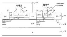
- a substrateincluding for example a silicon-on-insulator (SOI) layer 10 or the like is provided.
- An optional buried oxide layer (BOX) 12may also be formed on the SOI 10 with a silicon layer 14 on the BOX 12 .
- FIG. 1 afurther shows a pseudomorphic SiGe layer 16 is epitaxially grown on the silicon layer 14 , followed by another epitaxial silicon layer 18 .
- the thicknesses of the layersare in various ranges including.
- the BOX 12may be between 1200 ⁇ and 1600 ⁇
- the silicon layer 14may be between 10 ⁇ and 1000 ⁇ , preferably 700 ⁇ in thickness.
- the SiGe layer 16may be between 90 ⁇ and 500 ⁇ , preferably 400 ⁇ ; the Si layer 18 may be between 50 ⁇ and 400 ⁇ , preferably 300 ⁇ . It should be understood, though, that the thickness of these layers can vary, depending on the various design parameters of the device.
- the pseudomorphic SiGe layer 16is epitaxially grown in a conventional manner.
- the Ge contentmay be greater than 0% in ratio to the Si content, with a range, in embodiments, of between 20% to 30% being contemplated by the invention.
- the silicon layer 18 on the pseudomorphic SiGe layer 16can be deposited in a conventional manner via any selective epitaxial silicon formation technique, for example rapid thermal chemical vapor depositions (RTCVD) or molecular beam epitaxy (MBE) may be used to epitaxially grow device quality silicon.
- RTCVDrapid thermal chemical vapor depositions
- MBEmolecular beam epitaxy
- FIG. 1 bshows the separated channels (or device regions) formed by shallow trench isolation (STI) 20 .
- the insulating trenches 20are formed by conventional patterning processes including lithography and etching steps.
- the stacked layers 14 , 16 , 18are patterned to form STIs 20 using standard techniques of pad oxidation, pad nitride deposition, lithography based patterning, reactive ion etching (RIE) of the stacked layers, to the buried oxide.
- RIEreactive ion etching
- a liner deposition, fill deposition, and chemical mechanical polish, for example,can then be used to form the STI 20 .
- the STI formation processis well known in the art.
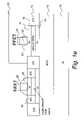
- FIG. 1 cdepicts the preparation of the gate electrodes.
- Placement of a polysilicon gates 22 capped with, for example, SiN layer 28is performed through conventional processing in both the NFET and PFET region of the device. This process includes lithography and etching steps.
- a polysilicon layer capped with a SiN protection layer 28is formed on the structure.
- a lithography processis applied which entails applying a photoresist on the SiN capped polysilicon layer, exposing the photoresist to a pattern of radiation, and developing the pattern utilizing a conventional resist developer.
- a conventional etching processsuch as RIE, plasma etching, ion beam etching, or laser ablation may be employed in transferring the pattern to active areas of the NFET region and PFET region to form SiN capped polysilicon gates 22 .
- polysilicon gates 22are capped with a SiN protection layer 28 . Sidewalls of the gates 22 are also protected with SiN, forming spacers 24 and 26 .
- the cap 28 and the polysilicon sidewall spacers 24 and 26are also formed in a conventional manner.
- a sacrificial block materialis deposited on the structure.
- the sacrificial materialis a nitride material (e.g., Si 3 N 4 ), which forms the SiN elements 24 , 26 and 28 .
- the layers 24 , 26 and 28can be formed in a conventional manner, such as by chemical vapor deposition (CVD) using a silane source.
- CVDchemical vapor deposition
- Other techniques which may be suitable for forming a nitride layerinclude LPCVD, and atmospheric pressure CVD (APCVD).
- the size of the polysilicon gates 22 and its sidewall spacers 24 and 26which cover the underlying layer 18 in the PFET and NFET region, respectively, ranges from 200 ⁇ to 1300 ⁇ . It should be understood that this is applicable for gate lengths centered around a nominal value (smallest size of the technology). For example, 400 ⁇ is a reasonable gate length for a 65 nm technology.
- the size of the gateis communicated in halfwidths.
- the halfwidthcomprises the size covered from the center of the gate to the outer edge of the spacer.
- the halfwidth of the NFET gateis larger than the halfwidth of the PFET gate.
- the larger NFET gate halfwidthwill result in a larger tensile stress in the NFET region due to a larger area covering the underlying SiGe material. Also, the smaller halfwidth of the PFET gate configuration results in a reduction of tensile stress which is imparted by the underlying SiGe layer. In this manner, a higher compressive stress component can be imparted on the PFET gate in subsequent processing steps.
- the polysilicon gates 22range in total size about 400 ⁇ , thus having a preferred halfwidth of 200 ⁇ (measured from the center to the edge).
- the spacer 26covers a size in the range of 50 ⁇ to 500 ⁇ , with a preferred range from 200 ⁇ to 300 ⁇ . Therefore, under preferred conditions and not limiting to the invention, the halfwidth of the NFET device ranges from 400 ⁇ to 500 ⁇ , however other combinations of the halfwidth of gate 22 and spacer 26 are contemplated.
- the size of spacer 24ranges from 50 ⁇ to 300 ⁇ , with 100 ⁇ being preferred; however shorter sizes of spacer 24 are contemplated.
- the halfwidth of the PFET gateranges from 250 ⁇ to 350 ⁇ .
- the different sizes of the spacersresults in higher tensile stress in the NFET channel region and reduces the tensile stress in the PFET channel region.
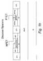
- FIGS. 1 d through 1 hshow the fabrication process of the gate structures, including the source and drain (S/D) regions for the NFET and PFET channel, respectively.
- a hard mask 30is placed onto the PFET region prior to the preparation of the S/D trenches in the NFET channel.
- the regions in the NFET adjacent to the stack formed by layers 16 , 18 , 28 , and 26are etched down ideally to the silicon layer 14 . This etching results in an elastic relaxation of the edges of the SiGe layer, creating a tensile strain placed on the upper Si layer, by the SiGe layer.
- FIG. 1 edepicts the device after epitaxial silicon 32 is selectively grown in the S/D trenches adjacent to the gate island formed by the SiGe and Si layers.
- the resulting gate islandresults in a longitudinal size between 400 ⁇ and 1300 ⁇ and has a preferred halfwidth range of 400 ⁇ to 500 ⁇ .
- the pseudomorphic SiGe layer 16 within the gate island in the NFET regionexercises a tensile stress onto the epitaxially grown Silicon 18 in the channel resulting in improved NFET device characteristics.
- FIG. 1 fanalogous to FIG. 1 d —presents the S/D preparation of the PFET region.
- a protective hard mask 30is placed over the NFET region and the S/D trenches adjacent to the stack formed by layers 16 , 18 , 22 , 24 , and 28 are etched down ideally to Si layer 14 .
- FIG. 1 gdepicts the filled S/D trenches of the PFET device.
- these trenchesare filled with SiGe material 34 , which is grown epitaxially.
- the longitudinal dimensions of these elementsare smaller to those described above for the NFET region.
- the PFET gate island formed by layers 16 and 18has a resulting size of 200 ⁇ to 400 ⁇ , resulting in a preferred halfwidth of 150 ⁇ .
- the SiGe material 34induces a compressive stress on the Si channel of the PFET device, resulting in improved PFET device characteristics.
- FIG. 1 hshows the fabricated CMOS device disposed of the sacrificial material.
- the ratio of the eSiGe material 34can vary between any germanium above 0% with respect to the total amount of silicon and germanium in the trench.
- FIG. 2 aillustrates the locations of the stresses in an NFET device according to the invention.
- tensile stressesare present in the channel of the NFET.
- the lattice structure of the SiGe layer 16matches the lattice structure of the underlying Si layer 14 . This results in the SiGe layer 16 and the surrounding areas being under a compressive stress.
- the edges of the SiGe layerwill undergo elastic relaxation, resulting in a tensile stress of the Si layer 18 in the channel.
- FIG. 2 billustrates the course of stress as a function of longitudinal distance to the center of the gate of the NFET device.
- the current inventionprovides tensile stresses in the range of about 300 MPa.
- the preferred range of the longitudinal stress component (stress in direction of current flow from source to drain) in the Si layer 18is preferred to be greater than 100 MPa.
- FIG. 2 balso shows that the tensile stresses extent laterally into the epitaxially grown Si elements 32 and tensile stresses above about 100 MPa reaches up to 150 ⁇ into the Si element 32 and reaches relaxation at about 250 ⁇ from the edge of the gate.
- FIG. 3show the course of stress as a function of the halfwidth with varying sizes of the thickness of SiGe layer 16 into the above lying silicon layers 18 .
- the Ge content of the SiGe layerranged from 20% to 30%.
- the halfwidth of the NFETranges from about 150 ⁇ to 500 ⁇ .
- high stressesabove 200 MPa can be triggered by varying the Ge content or the thickness of layer 16 .
- stress above about 200 MPacan be reached by either a 25% Ge-content and a thickness of about 400 ⁇ or a 30% Ge-content and a thickness of about 200 ⁇ .
- tensile stressesare now formed in the channel of NFET and compressive stresses are formed in the PFET.
- high device performancecan be achieved.
- the manufacturing costscan be reduced while resulting in higher yields.
Landscapes
- Insulated Gate Type Field-Effect Transistor (AREA)
- Metal-Oxide And Bipolar Metal-Oxide Semiconductor Integrated Circuits (AREA)
Abstract
Description
Claims (10)
Priority Applications (2)
| Application Number | Priority Date | Filing Date | Title |
|---|---|---|---|
| US11/380,688US7615418B2 (en) | 2006-04-28 | 2006-04-28 | High performance stress-enhance MOSFET and method of manufacture |
| CN2007100913700ACN101064285B (en) | 2006-04-28 | 2007-03-30 | High performance stress-enhance mosfet and method of manufacture |
Applications Claiming Priority (1)
| Application Number | Priority Date | Filing Date | Title |
|---|---|---|---|
| US11/380,688US7615418B2 (en) | 2006-04-28 | 2006-04-28 | High performance stress-enhance MOSFET and method of manufacture |
Publications (2)
| Publication Number | Publication Date |
|---|---|
| US20070254422A1 US20070254422A1 (en) | 2007-11-01 |
| US7615418B2true US7615418B2 (en) | 2009-11-10 |
Family
ID=38648817
Family Applications (1)
| Application Number | Title | Priority Date | Filing Date |
|---|---|---|---|
| US11/380,688Expired - Fee RelatedUS7615418B2 (en) | 2006-04-28 | 2006-04-28 | High performance stress-enhance MOSFET and method of manufacture |
Country Status (2)
| Country | Link |
|---|---|
| US (1) | US7615418B2 (en) |
| CN (1) | CN101064285B (en) |
Cited By (2)
| Publication number | Priority date | Publication date | Assignee | Title |
|---|---|---|---|---|
| US20120228639A1 (en)* | 2010-10-11 | 2012-09-13 | International Business Machines Corporation | Self aligned device with enhanced stress and methods of manufacture |
| US8476706B1 (en)* | 2012-01-04 | 2013-07-02 | International Business Machines Corporation | CMOS having a SiC/SiGe alloy stack |
Families Citing this family (6)
| Publication number | Priority date | Publication date | Assignee | Title |
|---|---|---|---|---|
| US8815660B2 (en)* | 2010-02-05 | 2014-08-26 | International Business Machines Corporation | Structure and method for reducing floating body effect of SOI MOSFETs |
| US8486776B2 (en)* | 2010-09-21 | 2013-07-16 | International Business Machines Corporation | Strained devices, methods of manufacture and design structures |
| US8946064B2 (en)* | 2011-06-16 | 2015-02-03 | International Business Machines Corporation | Transistor with buried silicon germanium for improved proximity control and optimized recess shape |
| US8642430B2 (en)* | 2012-04-09 | 2014-02-04 | GlobalFoundries, Inc. | Processes for preparing stressed semiconductor wafers and for preparing devices including the stressed semiconductor wafers |
| US10103064B2 (en)* | 2014-05-28 | 2018-10-16 | Taiwan Semiconductor Manufacturing Co., Ltd. | Transistor structure including epitaxial channel layers and raised source/drain regions |
| KR20170047953A (en)* | 2015-10-26 | 2017-05-08 | 삼성전자주식회사 | Semiconductor device and method of fabricating the same |
Citations (92)
| Publication number | Priority date | Publication date | Assignee | Title |
|---|---|---|---|---|
| US3602841A (en) | 1970-06-18 | 1971-08-31 | Ibm | High frequency bulk semiconductor amplifiers and oscillators |
| US4665415A (en) | 1985-04-24 | 1987-05-12 | International Business Machines Corporation | Semiconductor device with hole conduction via strained lattice |
| JPS6476755A (en) | 1987-09-18 | 1989-03-22 | Hitachi Ltd | Semiconductor device |
| US4853076A (en) | 1983-12-29 | 1989-08-01 | Massachusetts Institute Of Technology | Semiconductor thin films |
| US4855245A (en) | 1985-09-13 | 1989-08-08 | Siemens Aktiengesellschaft | Method of manufacturing integrated circuit containing bipolar and complementary MOS transistors on a common substrate |
| US4952524A (en) | 1989-05-05 | 1990-08-28 | At&T Bell Laboratories | Semiconductor device manufacture including trench formation |
| US4958213A (en) | 1987-12-07 | 1990-09-18 | Texas Instruments Incorporated | Method for forming a transistor base region under thick oxide |
| US5006913A (en) | 1988-11-05 | 1991-04-09 | Mitsubishi Denki Kabushiki Kaisha | Stacked type semiconductor device |
| US5060030A (en) | 1990-07-18 | 1991-10-22 | Raytheon Company | Pseudomorphic HEMT having strained compensation layer |
| US5081513A (en) | 1991-02-28 | 1992-01-14 | Xerox Corporation | Electronic device with recovery layer proximate to active layer |
| US5108843A (en) | 1988-11-30 | 1992-04-28 | Ricoh Company, Ltd. | Thin film semiconductor and process for producing the same |
| US5134085A (en) | 1991-11-21 | 1992-07-28 | Micron Technology, Inc. | Reduced-mask, split-polysilicon CMOS process, incorporating stacked-capacitor cells, for fabricating multi-megabit dynamic random access memories |
| US5310446A (en) | 1990-01-10 | 1994-05-10 | Ricoh Company, Ltd. | Method for producing semiconductor film |
| US5354695A (en) | 1992-04-08 | 1994-10-11 | Leedy Glenn J | Membrane dielectric isolation IC fabrication |
| US5371399A (en) | 1991-06-14 | 1994-12-06 | International Business Machines Corporation | Compound semiconductor having metallic inclusions and devices fabricated therefrom |
| US5391510A (en) | 1992-02-28 | 1995-02-21 | International Business Machines Corporation | Formation of self-aligned metal gate FETs using a benignant removable gate material during high temperature steps |
| US5459346A (en) | 1988-06-28 | 1995-10-17 | Ricoh Co., Ltd. | Semiconductor substrate with electrical contact in groove |
| US5557122A (en) | 1995-05-12 | 1996-09-17 | Alliance Semiconductors Corporation | Semiconductor electrode having improved grain structure and oxide growth properties |
| US5561302A (en) | 1994-09-26 | 1996-10-01 | Motorola, Inc. | Enhanced mobility MOSFET device and method |
| US5670798A (en) | 1995-03-29 | 1997-09-23 | North Carolina State University | Integrated heterostructures of Group III-V nitride semiconductor materials including epitaxial ohmic contact non-nitride buffer layer and methods of fabricating same |
| US5679965A (en) | 1995-03-29 | 1997-10-21 | North Carolina State University | Integrated heterostructures of Group III-V nitride semiconductor materials including epitaxial ohmic contact, non-nitride buffer layer and methods of fabricating same |
| US5861651A (en) | 1997-02-28 | 1999-01-19 | Lucent Technologies Inc. | Field effect devices and capacitors with improved thin film dielectrics and method for making same |
| US5880040A (en) | 1996-04-15 | 1999-03-09 | Macronix International Co., Ltd. | Gate dielectric based on oxynitride grown in N2 O and annealed in NO |
| US5940736A (en) | 1997-03-11 | 1999-08-17 | Lucent Technologies Inc. | Method for forming a high quality ultrathin gate oxide layer |
| US5940716A (en) | 1996-03-15 | 1999-08-17 | Samsung Electronics Co., Ltd. | Methods of forming trench isolation regions using repatterned trench masks |
| US5960297A (en) | 1997-07-02 | 1999-09-28 | Kabushiki Kaisha Toshiba | Shallow trench isolation structure and method of forming the same |
| US5989978A (en) | 1998-07-16 | 1999-11-23 | Chartered Semiconductor Manufacturing, Ltd. | Shallow trench isolation of MOSFETS with reduced corner parasitic currents |
| US6008126A (en) | 1992-04-08 | 1999-12-28 | Elm Technology Corporation | Membrane dielectric isolation IC fabrication |
| US6025280A (en) | 1997-04-28 | 2000-02-15 | Lucent Technologies Inc. | Use of SiD4 for deposition of ultra thin and controllable oxides |
| US6066545A (en) | 1997-12-09 | 2000-05-23 | Texas Instruments Incorporated | Birdsbeak encroachment using combination of wet and dry etch for isolation nitride |
| US6090684A (en) | 1998-07-31 | 2000-07-18 | Hitachi, Ltd. | Method for manufacturing semiconductor device |
| US6107143A (en) | 1998-03-02 | 2000-08-22 | Samsung Electronics Co., Ltd. | Method for forming a trench isolation structure in an integrated circuit |
| US6117722A (en) | 1999-02-18 | 2000-09-12 | Taiwan Semiconductor Manufacturing Company | SRAM layout for relaxing mechanical stress in shallow trench isolation technology and method of manufacture thereof |
| US6133071A (en) | 1997-10-15 | 2000-10-17 | Nec Corporation | Semiconductor device with plate heat sink free from cracks due to thermal stress and process for assembling it with package |
| US6165383A (en) | 1998-04-10 | 2000-12-26 | Organic Display Technology | Useful precursors for organic electroluminescent materials and devices made from such materials |
| US6221735B1 (en) | 2000-02-15 | 2001-04-24 | Philips Semiconductors, Inc. | Method for eliminating stress induced dislocations in CMOS devices |
| US6228694B1 (en) | 1999-06-28 | 2001-05-08 | Intel Corporation | Method of increasing the mobility of MOS transistors by use of localized stress regions |
| US6255169B1 (en) | 1999-02-22 | 2001-07-03 | Advanced Micro Devices, Inc. | Process for fabricating a high-endurance non-volatile memory device |
| US6261964B1 (en) | 1997-03-14 | 2001-07-17 | Micron Technology, Inc. | Material removal method for forming a structure |
| US6265317B1 (en) | 2001-01-09 | 2001-07-24 | Taiwan Semiconductor Manufacturing Company | Top corner rounding for shallow trench isolation |
| US20010009784A1 (en) | 1998-01-09 | 2001-07-26 | Yanjun Ma | Structure and method of making a sub-micron MOS transistor |
| US6274444B1 (en) | 1999-07-30 | 2001-08-14 | United Microelectronics Corp. | Method for forming mosfet |
| US6281532B1 (en) | 1999-06-28 | 2001-08-28 | Intel Corporation | Technique to obtain increased channel mobilities in NMOS transistors by gate electrode engineering |
| US6284623B1 (en) | 1999-10-25 | 2001-09-04 | Peng-Fei Zhang | Method of fabricating semiconductor devices using shallow trench isolation with reduced narrow channel effect |
| US6284626B1 (en) | 1999-04-06 | 2001-09-04 | Vantis Corporation | Angled nitrogen ion implantation for minimizing mechanical stress on side walls of an isolation trench |
| US6319794B1 (en) | 1998-10-14 | 2001-11-20 | International Business Machines Corporation | Structure and method for producing low leakage isolation devices |
| US6362082B1 (en) | 1999-06-28 | 2002-03-26 | Intel Corporation | Methodology for control of short channel effects in MOS transistors |
| US6361885B1 (en) | 1998-04-10 | 2002-03-26 | Organic Display Technology | Organic electroluminescent materials and device made from such materials |
| US6368931B1 (en) | 2000-03-27 | 2002-04-09 | Intel Corporation | Thin tensile layers in shallow trench isolation and method of making same |
| US20020063292A1 (en) | 2000-11-29 | 2002-05-30 | Mark Armstrong | CMOS fabrication process utilizing special transistor orientation |
| US6403486B1 (en) | 2001-04-30 | 2002-06-11 | Taiwan Semiconductor Manufacturing Company | Method for forming a shallow trench isolation |
| US6403975B1 (en) | 1996-04-09 | 2002-06-11 | Max-Planck Gesellschaft Zur Forderung Der Wissenschafteneev | Semiconductor components, in particular photodetectors, light emitting diodes, optical modulators and waveguides with multilayer structures grown on silicon substrates |
| US6406973B1 (en) | 1999-06-29 | 2002-06-18 | Hyundai Electronics Industries Co., Ltd. | Transistor in a semiconductor device and method of manufacturing the same |
| US20020086497A1 (en) | 2000-12-30 | 2002-07-04 | Kwok Siang Ping | Beaker shape trench with nitride pull-back for STI |
| US20020086472A1 (en) | 2000-12-29 | 2002-07-04 | Brian Roberds | Technique to obtain high mobility channels in MOS transistors by forming a strain layer on an underside of a channel |
| US20020090791A1 (en) | 1999-06-28 | 2002-07-11 | Brian S. Doyle | Method for reduced capacitance interconnect system using gaseous implants into the ild |
| US6461936B1 (en) | 2002-01-04 | 2002-10-08 | Infineon Technologies Ag | Double pullback method of filling an isolation trench |
| US6476462B2 (en) | 1999-12-28 | 2002-11-05 | Texas Instruments Incorporated | MOS-type semiconductor device and method for making same |
| US6483171B1 (en) | 1999-08-13 | 2002-11-19 | Micron Technology, Inc. | Vertical sub-micron CMOS transistors on (110), (111), (311), (511), and higher order surfaces of bulk, SOI and thin film structures and method of forming same |
| US6493497B1 (en) | 2000-09-26 | 2002-12-10 | Motorola, Inc. | Electro-optic structure and process for fabricating same |
| US6498358B1 (en) | 2001-07-20 | 2002-12-24 | Motorola, Inc. | Structure and method for fabricating an electro-optic system having an electrochromic diffraction grating |
| US6501121B1 (en) | 2000-11-15 | 2002-12-31 | Motorola, Inc. | Semiconductor structure |
| US6506652B2 (en) | 1998-11-13 | 2003-01-14 | Intel Corporation | Method of recessing spacers to improved salicide resistance on polysilicon gates |
| US20030032261A1 (en) | 2001-08-08 | 2003-02-13 | Ling-Yen Yeh | Method of preventing threshold voltage of MOS transistor from being decreased by shallow trench isolation formation |
| US20030040158A1 (en) | 2001-08-21 | 2003-02-27 | Nec Corporation | Semiconductor device and method of fabricating the same |
| US6531740B2 (en) | 2001-07-17 | 2003-03-11 | Motorola, Inc. | Integrated impedance matching and stability network |
| US6531369B1 (en) | 2000-03-01 | 2003-03-11 | Applied Micro Circuits Corporation | Heterojunction bipolar transistor (HBT) fabrication using a selectively deposited silicon germanium (SiGe) |
| US20030057184A1 (en) | 2001-09-22 | 2003-03-27 | Shiuh-Sheng Yu | Method for pull back SiN to increase rounding effect in a shallow trench isolation process |
| US20030067035A1 (en) | 2001-09-28 | 2003-04-10 | Helmut Tews | Gate processing method with reduced gate oxide corner and edge thinning |
| US6621392B1 (en) | 2002-04-25 | 2003-09-16 | International Business Machines Corporation | Micro electromechanical switch having self-aligned spacers |
| US6635506B2 (en) | 2001-11-07 | 2003-10-21 | International Business Machines Corporation | Method of fabricating micro-electromechanical switches on CMOS compatible substrates |
| US6696334B1 (en)* | 2002-09-30 | 2004-02-24 | Advanced Micro Devices, Inc. | Method for formation of a differential offset spacer |
| US6717216B1 (en) | 2002-12-12 | 2004-04-06 | International Business Machines Corporation | SOI based field effect transistor having a compressive film in undercut area under the channel and a method of making the device |
| US20040113174A1 (en) | 2002-12-12 | 2004-06-17 | International Business Machines Corporation | Isolation structures for imposing stress patterns |
| US20040113217A1 (en) | 2002-12-12 | 2004-06-17 | International Business Machines Corporation | Stress inducing spacers |
| US20040238914A1 (en) | 2003-05-30 | 2004-12-02 | International Business Machines Corporation | STI stress modification by nitrogen plasma treatment for improving performance in small width devices |
| US6831292B2 (en) | 2001-09-21 | 2004-12-14 | Amberwave Systems Corporation | Semiconductor structures employing strained material layers with defined impurity gradients and methods for fabricating same |
| US20040262784A1 (en) | 2003-06-30 | 2004-12-30 | International Business Machines Corporation | High performance cmos device structures and method of manufacture |
| US20050082634A1 (en) | 2003-10-16 | 2005-04-21 | International Business Machines Corporation | High performance strained cmos devices |
| US20050093030A1 (en) | 2003-10-30 | 2005-05-05 | Doris Bruce B. | Structure and method to enhance both nFET and pFET performance using different kinds of stressed layers |
| US20050098829A1 (en) | 2003-11-06 | 2005-05-12 | Doris Bruce B. | High mobility CMOS circuits |
| US20050106799A1 (en) | 2003-11-14 | 2005-05-19 | International Business Machines Corporation | Stressed semiconductor device structures having granular semiconductor material |
| US20050145954A1 (en) | 2004-01-05 | 2005-07-07 | International Business Machines Corporation | Structures and methods for making strained mosfets |
| US20050194699A1 (en) | 2004-03-03 | 2005-09-08 | International Business Machines Corporation | Mobility enhanced cmos devices |
| US20050236668A1 (en) | 2004-04-23 | 2005-10-27 | International Business Machines Corporation | STRUCTURES AND METHODS FOR MANUFACTURING OF DISLOCATION FREE STRESSED CHANNELS IN BULK SILICON AND SOI CMOS DEVICES BY GATE STRESS ENGINEERING WITH SiGe AND/OR Si:C |
| US20050245017A1 (en) | 2003-10-30 | 2005-11-03 | Belyansky Michael P | Structure and method to improve channel mobility by gate electrode stress modification |
| US20060057787A1 (en) | 2002-11-25 | 2006-03-16 | Doris Bruce B | Strained finfet cmos device structures |
| US20060060925A1 (en) | 2004-09-17 | 2006-03-23 | International Business Machines Corporation | Semiconductor device structure with active regions having different surface directions and methods |
| US20060228851A1 (en)* | 2005-03-30 | 2006-10-12 | Sadaka Mariam G | Method of making a dual strained channel semiconductor device |
| US20060286736A1 (en)* | 2005-06-15 | 2006-12-21 | Freescale Semiconductor, Inc. | Method for forming an electronic device |
| US7217608B1 (en)* | 2001-12-17 | 2007-05-15 | Advanced Micro Devices, Inc. | CMOS with strained silicon channel NMOS and silicon germanium channel PMOS |
| US7335929B2 (en)* | 2004-10-18 | 2008-02-26 | Taiwan Semiconductor Manufacturing Company, Ltd. | Transistor with a strained region and method of manufacture |
- 2006
- 2006-04-28USUS11/380,688patent/US7615418B2/ennot_activeExpired - Fee Related
- 2007
- 2007-03-30CNCN2007100913700Apatent/CN101064285B/ennot_activeExpired - Fee Related
Patent Citations (114)
| Publication number | Priority date | Publication date | Assignee | Title |
|---|---|---|---|---|
| US3602841A (en) | 1970-06-18 | 1971-08-31 | Ibm | High frequency bulk semiconductor amplifiers and oscillators |
| US4853076A (en) | 1983-12-29 | 1989-08-01 | Massachusetts Institute Of Technology | Semiconductor thin films |
| US4665415A (en) | 1985-04-24 | 1987-05-12 | International Business Machines Corporation | Semiconductor device with hole conduction via strained lattice |
| US4855245A (en) | 1985-09-13 | 1989-08-08 | Siemens Aktiengesellschaft | Method of manufacturing integrated circuit containing bipolar and complementary MOS transistors on a common substrate |
| JPS6476755A (en) | 1987-09-18 | 1989-03-22 | Hitachi Ltd | Semiconductor device |
| US4958213A (en) | 1987-12-07 | 1990-09-18 | Texas Instruments Incorporated | Method for forming a transistor base region under thick oxide |
| US5459346A (en) | 1988-06-28 | 1995-10-17 | Ricoh Co., Ltd. | Semiconductor substrate with electrical contact in groove |
| US5565697A (en) | 1988-06-28 | 1996-10-15 | Ricoh Company, Ltd. | Semiconductor structure having island forming grooves |
| US5006913A (en) | 1988-11-05 | 1991-04-09 | Mitsubishi Denki Kabushiki Kaisha | Stacked type semiconductor device |
| US5108843A (en) | 1988-11-30 | 1992-04-28 | Ricoh Company, Ltd. | Thin film semiconductor and process for producing the same |
| US4952524A (en) | 1989-05-05 | 1990-08-28 | At&T Bell Laboratories | Semiconductor device manufacture including trench formation |
| US5310446A (en) | 1990-01-10 | 1994-05-10 | Ricoh Company, Ltd. | Method for producing semiconductor film |
| US5060030A (en) | 1990-07-18 | 1991-10-22 | Raytheon Company | Pseudomorphic HEMT having strained compensation layer |
| US5081513A (en) | 1991-02-28 | 1992-01-14 | Xerox Corporation | Electronic device with recovery layer proximate to active layer |
| US5371399A (en) | 1991-06-14 | 1994-12-06 | International Business Machines Corporation | Compound semiconductor having metallic inclusions and devices fabricated therefrom |
| US5471948A (en) | 1991-06-14 | 1995-12-05 | International Business Machines Corporation | Method of making a compound semiconductor having metallic inclusions |
| US5134085A (en) | 1991-11-21 | 1992-07-28 | Micron Technology, Inc. | Reduced-mask, split-polysilicon CMOS process, incorporating stacked-capacitor cells, for fabricating multi-megabit dynamic random access memories |
| US5391510A (en) | 1992-02-28 | 1995-02-21 | International Business Machines Corporation | Formation of self-aligned metal gate FETs using a benignant removable gate material during high temperature steps |
| US5354695A (en) | 1992-04-08 | 1994-10-11 | Leedy Glenn J | Membrane dielectric isolation IC fabrication |
| US5840593A (en) | 1992-04-08 | 1998-11-24 | Elm Technology Corporation | Membrane dielectric isolation IC fabrication |
| US5571741A (en) | 1992-04-08 | 1996-11-05 | Leedy; Glenn J. | Membrane dielectric isolation IC fabrication |
| US5592018A (en) | 1992-04-08 | 1997-01-07 | Leedy; Glenn J. | Membrane dielectric isolation IC fabrication |
| US5592007A (en) | 1992-04-08 | 1997-01-07 | Leedy; Glenn J. | Membrane dielectric isolation transistor fabrication |
| US6008126A (en) | 1992-04-08 | 1999-12-28 | Elm Technology Corporation | Membrane dielectric isolation IC fabrication |
| US5946559A (en) | 1992-04-08 | 1999-08-31 | Elm Technology Corporation | Membrane dielectric isolation IC fabrication |
| US5561302A (en) | 1994-09-26 | 1996-10-01 | Motorola, Inc. | Enhanced mobility MOSFET device and method |
| US5683934A (en) | 1994-09-26 | 1997-11-04 | Motorola, Inc. | Enhanced mobility MOSFET device and method |
| US5670798A (en) | 1995-03-29 | 1997-09-23 | North Carolina State University | Integrated heterostructures of Group III-V nitride semiconductor materials including epitaxial ohmic contact non-nitride buffer layer and methods of fabricating same |
| US5679965A (en) | 1995-03-29 | 1997-10-21 | North Carolina State University | Integrated heterostructures of Group III-V nitride semiconductor materials including epitaxial ohmic contact, non-nitride buffer layer and methods of fabricating same |
| US6046464A (en) | 1995-03-29 | 2000-04-04 | North Carolina State University | Integrated heterostructures of group III-V nitride semiconductor materials including epitaxial ohmic contact comprising multiple quantum well |
| US5557122A (en) | 1995-05-12 | 1996-09-17 | Alliance Semiconductors Corporation | Semiconductor electrode having improved grain structure and oxide growth properties |
| US5940716A (en) | 1996-03-15 | 1999-08-17 | Samsung Electronics Co., Ltd. | Methods of forming trench isolation regions using repatterned trench masks |
| US6403975B1 (en) | 1996-04-09 | 2002-06-11 | Max-Planck Gesellschaft Zur Forderung Der Wissenschafteneev | Semiconductor components, in particular photodetectors, light emitting diodes, optical modulators and waveguides with multilayer structures grown on silicon substrates |
| US5880040A (en) | 1996-04-15 | 1999-03-09 | Macronix International Co., Ltd. | Gate dielectric based on oxynitride grown in N2 O and annealed in NO |
| US5861651A (en) | 1997-02-28 | 1999-01-19 | Lucent Technologies Inc. | Field effect devices and capacitors with improved thin film dielectrics and method for making same |
| US6246095B1 (en) | 1997-03-11 | 2001-06-12 | Agere Systems Guardian Corp. | System and method for forming a uniform thin gate oxide layer |
| US5940736A (en) | 1997-03-11 | 1999-08-17 | Lucent Technologies Inc. | Method for forming a high quality ultrathin gate oxide layer |
| US6261964B1 (en) | 1997-03-14 | 2001-07-17 | Micron Technology, Inc. | Material removal method for forming a structure |
| US6025280A (en) | 1997-04-28 | 2000-02-15 | Lucent Technologies Inc. | Use of SiD4 for deposition of ultra thin and controllable oxides |
| US5960297A (en) | 1997-07-02 | 1999-09-28 | Kabushiki Kaisha Toshiba | Shallow trench isolation structure and method of forming the same |
| US6133071A (en) | 1997-10-15 | 2000-10-17 | Nec Corporation | Semiconductor device with plate heat sink free from cracks due to thermal stress and process for assembling it with package |
| US6066545A (en) | 1997-12-09 | 2000-05-23 | Texas Instruments Incorporated | Birdsbeak encroachment using combination of wet and dry etch for isolation nitride |
| US20010009784A1 (en) | 1998-01-09 | 2001-07-26 | Yanjun Ma | Structure and method of making a sub-micron MOS transistor |
| US6107143A (en) | 1998-03-02 | 2000-08-22 | Samsung Electronics Co., Ltd. | Method for forming a trench isolation structure in an integrated circuit |
| US6165383A (en) | 1998-04-10 | 2000-12-26 | Organic Display Technology | Useful precursors for organic electroluminescent materials and devices made from such materials |
| US6361885B1 (en) | 1998-04-10 | 2002-03-26 | Organic Display Technology | Organic electroluminescent materials and device made from such materials |
| US5989978A (en) | 1998-07-16 | 1999-11-23 | Chartered Semiconductor Manufacturing, Ltd. | Shallow trench isolation of MOSFETS with reduced corner parasitic currents |
| US6090684A (en) | 1998-07-31 | 2000-07-18 | Hitachi, Ltd. | Method for manufacturing semiconductor device |
| US6319794B1 (en) | 1998-10-14 | 2001-11-20 | International Business Machines Corporation | Structure and method for producing low leakage isolation devices |
| US6521964B1 (en) | 1998-11-13 | 2003-02-18 | Intel Corporation | Device having spacers for improved salicide resistance on polysilicon gates |
| US6506652B2 (en) | 1998-11-13 | 2003-01-14 | Intel Corporation | Method of recessing spacers to improved salicide resistance on polysilicon gates |
| US6509618B2 (en) | 1998-11-13 | 2003-01-21 | Intel Corporation | Device having thin first spacers and partially recessed thick second spacers for improved salicide resistance on polysilicon gates |
| US6117722A (en) | 1999-02-18 | 2000-09-12 | Taiwan Semiconductor Manufacturing Company | SRAM layout for relaxing mechanical stress in shallow trench isolation technology and method of manufacture thereof |
| US6255169B1 (en) | 1999-02-22 | 2001-07-03 | Advanced Micro Devices, Inc. | Process for fabricating a high-endurance non-volatile memory device |
| US6284626B1 (en) | 1999-04-06 | 2001-09-04 | Vantis Corporation | Angled nitrogen ion implantation for minimizing mechanical stress on side walls of an isolation trench |
| US6228694B1 (en) | 1999-06-28 | 2001-05-08 | Intel Corporation | Method of increasing the mobility of MOS transistors by use of localized stress regions |
| US6362082B1 (en) | 1999-06-28 | 2002-03-26 | Intel Corporation | Methodology for control of short channel effects in MOS transistors |
| US6281532B1 (en) | 1999-06-28 | 2001-08-28 | Intel Corporation | Technique to obtain increased channel mobilities in NMOS transistors by gate electrode engineering |
| US20020090791A1 (en) | 1999-06-28 | 2002-07-11 | Brian S. Doyle | Method for reduced capacitance interconnect system using gaseous implants into the ild |
| US20020074598A1 (en) | 1999-06-28 | 2002-06-20 | Doyle Brian S. | Methodology for control of short channel effects in MOS transistors |
| US6406973B1 (en) | 1999-06-29 | 2002-06-18 | Hyundai Electronics Industries Co., Ltd. | Transistor in a semiconductor device and method of manufacturing the same |
| US6274444B1 (en) | 1999-07-30 | 2001-08-14 | United Microelectronics Corp. | Method for forming mosfet |
| US6483171B1 (en) | 1999-08-13 | 2002-11-19 | Micron Technology, Inc. | Vertical sub-micron CMOS transistors on (110), (111), (311), (511), and higher order surfaces of bulk, SOI and thin film structures and method of forming same |
| US6284623B1 (en) | 1999-10-25 | 2001-09-04 | Peng-Fei Zhang | Method of fabricating semiconductor devices using shallow trench isolation with reduced narrow channel effect |
| US6476462B2 (en) | 1999-12-28 | 2002-11-05 | Texas Instruments Incorporated | MOS-type semiconductor device and method for making same |
| US6221735B1 (en) | 2000-02-15 | 2001-04-24 | Philips Semiconductors, Inc. | Method for eliminating stress induced dislocations in CMOS devices |
| US6531369B1 (en) | 2000-03-01 | 2003-03-11 | Applied Micro Circuits Corporation | Heterojunction bipolar transistor (HBT) fabrication using a selectively deposited silicon germanium (SiGe) |
| US6368931B1 (en) | 2000-03-27 | 2002-04-09 | Intel Corporation | Thin tensile layers in shallow trench isolation and method of making same |
| US6493497B1 (en) | 2000-09-26 | 2002-12-10 | Motorola, Inc. | Electro-optic structure and process for fabricating same |
| US6501121B1 (en) | 2000-11-15 | 2002-12-31 | Motorola, Inc. | Semiconductor structure |
| US20020063292A1 (en) | 2000-11-29 | 2002-05-30 | Mark Armstrong | CMOS fabrication process utilizing special transistor orientation |
| US20020086472A1 (en) | 2000-12-29 | 2002-07-04 | Brian Roberds | Technique to obtain high mobility channels in MOS transistors by forming a strain layer on an underside of a channel |
| US20020086497A1 (en) | 2000-12-30 | 2002-07-04 | Kwok Siang Ping | Beaker shape trench with nitride pull-back for STI |
| US6265317B1 (en) | 2001-01-09 | 2001-07-24 | Taiwan Semiconductor Manufacturing Company | Top corner rounding for shallow trench isolation |
| US6403486B1 (en) | 2001-04-30 | 2002-06-11 | Taiwan Semiconductor Manufacturing Company | Method for forming a shallow trench isolation |
| US6531740B2 (en) | 2001-07-17 | 2003-03-11 | Motorola, Inc. | Integrated impedance matching and stability network |
| US6498358B1 (en) | 2001-07-20 | 2002-12-24 | Motorola, Inc. | Structure and method for fabricating an electro-optic system having an electrochromic diffraction grating |
| US20030032261A1 (en) | 2001-08-08 | 2003-02-13 | Ling-Yen Yeh | Method of preventing threshold voltage of MOS transistor from being decreased by shallow trench isolation formation |
| US20030040158A1 (en) | 2001-08-21 | 2003-02-27 | Nec Corporation | Semiconductor device and method of fabricating the same |
| US6831292B2 (en) | 2001-09-21 | 2004-12-14 | Amberwave Systems Corporation | Semiconductor structures employing strained material layers with defined impurity gradients and methods for fabricating same |
| US20030057184A1 (en) | 2001-09-22 | 2003-03-27 | Shiuh-Sheng Yu | Method for pull back SiN to increase rounding effect in a shallow trench isolation process |
| US20030067035A1 (en) | 2001-09-28 | 2003-04-10 | Helmut Tews | Gate processing method with reduced gate oxide corner and edge thinning |
| US6635506B2 (en) | 2001-11-07 | 2003-10-21 | International Business Machines Corporation | Method of fabricating micro-electromechanical switches on CMOS compatible substrates |
| US7217608B1 (en)* | 2001-12-17 | 2007-05-15 | Advanced Micro Devices, Inc. | CMOS with strained silicon channel NMOS and silicon germanium channel PMOS |
| US6461936B1 (en) | 2002-01-04 | 2002-10-08 | Infineon Technologies Ag | Double pullback method of filling an isolation trench |
| US6621392B1 (en) | 2002-04-25 | 2003-09-16 | International Business Machines Corporation | Micro electromechanical switch having self-aligned spacers |
| US6696334B1 (en)* | 2002-09-30 | 2004-02-24 | Advanced Micro Devices, Inc. | Method for formation of a differential offset spacer |
| US20060057787A1 (en) | 2002-11-25 | 2006-03-16 | Doris Bruce B | Strained finfet cmos device structures |
| US20050040460A1 (en) | 2002-12-12 | 2005-02-24 | Dureseti Chidambarrao | Stress inducing spacers |
| US6717216B1 (en) | 2002-12-12 | 2004-04-06 | International Business Machines Corporation | SOI based field effect transistor having a compressive film in undercut area under the channel and a method of making the device |
| US6825529B2 (en) | 2002-12-12 | 2004-11-30 | International Business Machines Corporation | Stress inducing spacers |
| US6974981B2 (en) | 2002-12-12 | 2005-12-13 | International Business Machines Corporation | Isolation structures for imposing stress patterns |
| US20050280051A1 (en) | 2002-12-12 | 2005-12-22 | Dureseti Chidambarrao | Isolation structures for imposing stress patterns |
| US20040113174A1 (en) | 2002-12-12 | 2004-06-17 | International Business Machines Corporation | Isolation structures for imposing stress patterns |
| US20040113217A1 (en) | 2002-12-12 | 2004-06-17 | International Business Machines Corporation | Stress inducing spacers |
| US20040238914A1 (en) | 2003-05-30 | 2004-12-02 | International Business Machines Corporation | STI stress modification by nitrogen plasma treatment for improving performance in small width devices |
| US20040262784A1 (en) | 2003-06-30 | 2004-12-30 | International Business Machines Corporation | High performance cmos device structures and method of manufacture |
| US20050082634A1 (en) | 2003-10-16 | 2005-04-21 | International Business Machines Corporation | High performance strained cmos devices |
| US20050148146A1 (en) | 2003-10-16 | 2005-07-07 | Doris Bruce D. | High performance strained CMOS devices |
| US20050093030A1 (en) | 2003-10-30 | 2005-05-05 | Doris Bruce B. | Structure and method to enhance both nFET and pFET performance using different kinds of stressed layers |
| US6977194B2 (en) | 2003-10-30 | 2005-12-20 | International Business Machines Corporation | Structure and method to improve channel mobility by gate electrode stress modification |
| US20050282325A1 (en) | 2003-10-30 | 2005-12-22 | Belyansky Michael P | Structure and method to improve channel mobility by gate electrode stress modification |
| US20050245017A1 (en) | 2003-10-30 | 2005-11-03 | Belyansky Michael P | Structure and method to improve channel mobility by gate electrode stress modification |
| US20060027868A1 (en) | 2003-11-06 | 2006-02-09 | Ibm Corporation | High mobility CMOS circuits |
| US7015082B2 (en) | 2003-11-06 | 2006-03-21 | International Business Machines Corporation | High mobility CMOS circuits |
| US20050098829A1 (en) | 2003-11-06 | 2005-05-12 | Doris Bruce B. | High mobility CMOS circuits |
| US20050106799A1 (en) | 2003-11-14 | 2005-05-19 | International Business Machines Corporation | Stressed semiconductor device structures having granular semiconductor material |
| US20050145954A1 (en) | 2004-01-05 | 2005-07-07 | International Business Machines Corporation | Structures and methods for making strained mosfets |
| US20050194699A1 (en) | 2004-03-03 | 2005-09-08 | International Business Machines Corporation | Mobility enhanced cmos devices |
| US20050236668A1 (en) | 2004-04-23 | 2005-10-27 | International Business Machines Corporation | STRUCTURES AND METHODS FOR MANUFACTURING OF DISLOCATION FREE STRESSED CHANNELS IN BULK SILICON AND SOI CMOS DEVICES BY GATE STRESS ENGINEERING WITH SiGe AND/OR Si:C |
| US20060060925A1 (en) | 2004-09-17 | 2006-03-23 | International Business Machines Corporation | Semiconductor device structure with active regions having different surface directions and methods |
| US7335929B2 (en)* | 2004-10-18 | 2008-02-26 | Taiwan Semiconductor Manufacturing Company, Ltd. | Transistor with a strained region and method of manufacture |
| US20060228851A1 (en)* | 2005-03-30 | 2006-10-12 | Sadaka Mariam G | Method of making a dual strained channel semiconductor device |
| US20060286736A1 (en)* | 2005-06-15 | 2006-12-21 | Freescale Semiconductor, Inc. | Method for forming an electronic device |
Non-Patent Citations (24)
Cited By (4)
| Publication number | Priority date | Publication date | Assignee | Title |
|---|---|---|---|---|
| US20120228639A1 (en)* | 2010-10-11 | 2012-09-13 | International Business Machines Corporation | Self aligned device with enhanced stress and methods of manufacture |
| US9293593B2 (en)* | 2010-10-11 | 2016-03-22 | Globalfoundries Inc. | Self aligned device with enhanced stress and methods of manufacture |
| US8476706B1 (en)* | 2012-01-04 | 2013-07-02 | International Business Machines Corporation | CMOS having a SiC/SiGe alloy stack |
| US8835234B2 (en) | 2012-01-04 | 2014-09-16 | International Business Machines Corporation | MOS having a sic/sige alloy stack |
Also Published As
| Publication number | Publication date |
|---|---|
| CN101064285A (en) | 2007-10-31 |
| CN101064285B (en) | 2012-03-21 |
| US20070254422A1 (en) | 2007-11-01 |
Similar Documents
| Publication | Publication Date | Title |
|---|---|---|
| US7608489B2 (en) | High performance stress-enhance MOSFET and method of manufacture | |
| US7560326B2 (en) | Silicon/silcion germaninum/silicon body device with embedded carbon dopant | |
| US8168489B2 (en) | High performance stress-enhanced MOSFETS using Si:C and SiGe epitaxial source/drain and method of manufacture | |
| US8168971B2 (en) | Pseudomorphic Si/SiGe/Si body device with embedded SiGe source/drain | |
| US7843024B2 (en) | Method and structure for improving device performance variation in dual stress liner technology | |
| US7615418B2 (en) | High performance stress-enhance MOSFET and method of manufacture | |
| US9431535B2 (en) | Semiconductor devices having tensile and/or compressive stress and methods of manufacturing | |
| US20080128765A1 (en) | MOSFET Device With Localized Stressor | |
| US7223994B2 (en) | Strained Si on multiple materials for bulk or SOI substrates | |
| US20060163608A1 (en) | Protecting silicon germanium sidewall with silicon for strained silicon silicon mosfets | |
| US8736016B2 (en) | Strained isolation regions | |
| US7518188B2 (en) | P-channel MOS transistor and fabrication process thereof |
Legal Events
| Date | Code | Title | Description |
|---|---|---|---|
| AS | Assignment | Owner name:INTERNATIONAL BUSINESS MACHINES CORPORATION, NEW Y Free format text:ASSIGNMENT OF ASSIGNORS INTEREST;ASSIGNORS:CHIDAMBARRAO, DURESETI;DONATON, RICARDO A.;HENSON, WILLIAM K.;AND OTHERS;REEL/FRAME:017578/0190;SIGNING DATES FROM 20060420 TO 20060424 | |
| FEPP | Fee payment procedure | Free format text:PAYOR NUMBER ASSIGNED (ORIGINAL EVENT CODE: ASPN); ENTITY STATUS OF PATENT OWNER: LARGE ENTITY | |
| STCF | Information on status: patent grant | Free format text:PATENTED CASE | |
| FPAY | Fee payment | Year of fee payment:4 | |
| AS | Assignment | Owner name:GLOBALFOUNDRIES U.S. 2 LLC, NEW YORK Free format text:ASSIGNMENT OF ASSIGNORS INTEREST;ASSIGNOR:INTERNATIONAL BUSINESS MACHINES CORPORATION;REEL/FRAME:036550/0001 Effective date:20150629 | |
| AS | Assignment | Owner name:GLOBALFOUNDRIES INC., CAYMAN ISLANDS Free format text:ASSIGNMENT OF ASSIGNORS INTEREST;ASSIGNORS:GLOBALFOUNDRIES U.S. 2 LLC;GLOBALFOUNDRIES U.S. INC.;REEL/FRAME:036779/0001 Effective date:20150910 | |
| FPAY | Fee payment | Year of fee payment:8 | |
| AS | Assignment | Owner name:WILMINGTON TRUST, NATIONAL ASSOCIATION, DELAWARE Free format text:SECURITY AGREEMENT;ASSIGNOR:GLOBALFOUNDRIES INC.;REEL/FRAME:049490/0001 Effective date:20181127 | |
| AS | Assignment | Owner name:GLOBALFOUNDRIES INC., CAYMAN ISLANDS Free format text:RELEASE BY SECURED PARTY;ASSIGNOR:WILMINGTON TRUST, NATIONAL ASSOCIATION;REEL/FRAME:054479/0842 Effective date:20200410 Owner name:TAIWAN SEMICONDUCTOR MANUFACTURING CO., LTD., TAIWAN Free format text:ASSIGNMENT OF ASSIGNORS INTEREST;ASSIGNOR:GLOBALFOUNDRIES INC.;REEL/FRAME:054482/0862 Effective date:20200515 | |
| AS | Assignment | Owner name:GLOBALFOUNDRIES INC., CAYMAN ISLANDS Free format text:RELEASE BY SECURED PARTY;ASSIGNOR:WILMINGTON TRUST, NATIONAL ASSOCIATION;REEL/FRAME:054636/0001 Effective date:20201117 | |
| FEPP | Fee payment procedure | Free format text:MAINTENANCE FEE REMINDER MAILED (ORIGINAL EVENT CODE: REM.); ENTITY STATUS OF PATENT OWNER: LARGE ENTITY | |
| LAPS | Lapse for failure to pay maintenance fees | Free format text:PATENT EXPIRED FOR FAILURE TO PAY MAINTENANCE FEES (ORIGINAL EVENT CODE: EXP.); ENTITY STATUS OF PATENT OWNER: LARGE ENTITY | |
| STCH | Information on status: patent discontinuation | Free format text:PATENT EXPIRED DUE TO NONPAYMENT OF MAINTENANCE FEES UNDER 37 CFR 1.362 | |
| FP | Lapsed due to failure to pay maintenance fee | Effective date:20211110 |