US7614777B2 - Liquid crystal display device - Google Patents
Liquid crystal display deviceDownload PDFInfo
- Publication number
- US7614777B2 US7614777B2US11/729,777US72977707AUS7614777B2US 7614777 B2US7614777 B2US 7614777B2US 72977707 AUS72977707 AUS 72977707AUS 7614777 B2US7614777 B2US 7614777B2
- Authority
- US
- United States
- Prior art keywords
- light
- inclined surface
- guide plate
- light guide
- liquid crystal
- Prior art date
- Legal status (The legal status is an assumption and is not a legal conclusion. Google has not performed a legal analysis and makes no representation as to the accuracy of the status listed.)
- Expired - Fee Related
Links
Images


Classifications
- G—PHYSICS
- G02—OPTICS
- G02B—OPTICAL ELEMENTS, SYSTEMS OR APPARATUS
- G02B6/00—Light guides; Structural details of arrangements comprising light guides and other optical elements, e.g. couplings
- G02B6/0001—Light guides; Structural details of arrangements comprising light guides and other optical elements, e.g. couplings specially adapted for lighting devices or systems
- G02B6/0011—Light guides; Structural details of arrangements comprising light guides and other optical elements, e.g. couplings specially adapted for lighting devices or systems the light guides being planar or of plate-like form
- G02B6/0066—Light guides; Structural details of arrangements comprising light guides and other optical elements, e.g. couplings specially adapted for lighting devices or systems the light guides being planar or of plate-like form characterised by the light source being coupled to the light guide
- G02B6/0068—Arrangements of plural sources, e.g. multi-colour light sources
- G—PHYSICS
- G02—OPTICS
- G02B—OPTICAL ELEMENTS, SYSTEMS OR APPARATUS
- G02B6/00—Light guides; Structural details of arrangements comprising light guides and other optical elements, e.g. couplings
- G02B6/0001—Light guides; Structural details of arrangements comprising light guides and other optical elements, e.g. couplings specially adapted for lighting devices or systems
- G02B6/0011—Light guides; Structural details of arrangements comprising light guides and other optical elements, e.g. couplings specially adapted for lighting devices or systems the light guides being planar or of plate-like form
- G02B6/0033—Means for improving the coupling-out of light from the light guide
- G02B6/0035—Means for improving the coupling-out of light from the light guide provided on the surface of the light guide or in the bulk of it
- G02B6/0036—2-D arrangement of prisms, protrusions, indentations or roughened surfaces
Definitions
- the present inventionrelates to a non-self-luminous display device, and more particularly to a liquid crystal display device having a flat lighting device which includes a light guide plate on a back surface of a liquid crystal display panel and uses a light emitting element as a light source.
- the present inventionrelates to the light diffusion structure of the light guide plate.
- the liquid crystal display devicehas been popularly used as a display device.
- the liquid crystal display deviceis used as a display part of portable equipment because of a reduced thickness, a reduced weight and low electric power consumption.
- the liquid crystal display deviceis not self-luminous and hence, the display device requires an illumination means.
- an illumination device which is used for the liquid crystal display devicea flat lighting device referred to as a backlight is popularly used.
- a cold cathode fluorescence lamphas been used as a light emitting element of the backlight
- an LEDhas been also recently used as the light emitting element in the portable equipment.
- the backlightusually includes a plate-like light guide plate.
- the light guide plateis made of a light-transmissive resin material, and light which is incident on the light guide plate from a light emitting element pass through the inside of the light guide plate. Reflection members, light diffusion members or the like such as grooves or projections are formed on the light guide plate, and the light which passes through in the inside of the light guide plate is radiated toward a back surface of a liquid crystal display panel by the reflection members or the light diffusion members.
- JP-A-2005-331565 or the likeproposes a liquid crystal display device which uses LEDs as light emitting elements, arranges a plurality of LEDs on a plurality of corner portions of a light guide plate, and forms concentric arcuate inclined surfaces about the LEDs which reflect the light on the light guide plate.
- the backlightwhich uses a plurality of LEDs for increasing the brightness as the light emitting element
- a plurality of light emitting pointsexist and hence, positions and shapes of members which reflect and radiate the light passing through the inside of the light guide plate become complicated.
- the LEDsare arranged at the corner portions of the light guide plate in consideration of spreading of the light radiated from the LEDs, there has been a drawback that it is difficult to set an angle of a reflection surface of one reflection member so as to reflect the light from two directions toward a radiation surface side.
- the present inventionhas been made to overcome the above-mentioned conventional drawback, and it is an object of the present invention to provide a liquid crystal display device which can obtain a display image of high quality with the acquisition of high brightness and uniform brightness distribution of by focusing the light radiation direction from a light guide plate in the vertical direction with respect to a light radiation surface of the light guide plate.
- a liquid crystal display devicewhich includes a liquid crystal display panel which is configured such that a liquid crystal layer is sandwiched between a pair of transparent substrates which have electrodes for forming pixels on an inner surface of the transparent substrate, and a backlight which radiates an illumination light to the back surface of the liquid crystal panel, wherein the backlight includes light emitting elements, a light guide plate on which light is incident from the light emitting elements, a first inclined surface which is arranged to face the light emitting elements formed on the light guide plate, and a second inclined surface which is brought into contact with the first inclined surface.
- the liquid crystal display devicemay preferably be configured such that, in the above-mentioned constitution, the light radiation direction of the light from the light guide plate is focused in the vertical direction with respect to a light radiation surface by setting the first inclined surface and the second inclined surface to a value which falls within a range of 45° to 65° with respect to a bottom surface of the light guide plate.
- a light utilization efficiencycan be largely enhanced whereby high brightness and uniform brightness distribution of light can be obtained. Accordingly, it is possible to achieve an advantageous effect to realize a liquid crystal display device of high display quality.
- FIG. 1is a plan view showing the schematic constitution of a liquid crystal display device of an embodiment according to the present invention
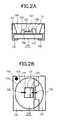
- FIG. 2A and FIG. 2Bare views showing the schematic structure of a LED of the liquid crystal display device, wherein FIG. 2A is a cross-sectional view of the LED, and FIG. 2B is a plan view of a light emitting surface side of the LED;
- FIG. 3A and FIG. 3Bare views showing the schematic constitution of a light guide plate, wherein FIG. 3A is a plan view of the light guide plate, and FIG. 3B is a side view of the light guide plate;
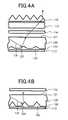
- FIG. 4A and FIG. 4Bare schematic cross-sectional views showing the propagation of light in the inside of the light guide plate, wherein FIG. 4A is a view showing an existing light propagation state, and FIG. 4B is a view showing a light propagation state of the embodiment according to the present invention;
- FIG. 5is a schematic plan view showing drawbacks when a plurality of light emitting elements are used for the liquid crystal display device
- FIG. 6is a schematic perspective view showing drawbacks when a plurality of light emitting elements are used for the liquid crystal display device
- FIG. 7is a schematic perspective view showing inclined surfaces
- FIG. 8is a schematic perspective view showing reflection members
- FIG. 9is a schematic plan view showing a light guide plate
- FIG. 10is a schematic plan view showing the light guide plate
- FIG. 11is a schematic cross-sectional view showing the light guide plate
- FIG. 12is a view showing the radiation brightness from the light guide plate
- FIG. 13is a view showing the radiation brightness from the light guide plate
- FIG. 14is a schematic perspective view showing angles at which the radiation brightness shown in FIG. 12 and FIG. 13 is measured in the light guide plate.
- FIG. 15is a schematic cross-sectional view showing the constitution of the light guide plate.
- FIG. 1is a plan view of an essential part showing the whole constitution according to one example of a liquid crystal display device of the present invention.
- the liquid crystal display device 100is constituted of a liquid crystal display panel 1 , a backlight 110 and a control circuit 80 .
- the liquid crystal display panel 1is formed by sealing a liquid crystal layer between glass substrates having electrodes for forming pixels. Signals and power source voltages necessary for display using liquid crystal are supplied to the liquid crystal display panel 1 from the control circuit 80 .
- the control circuit 80is mounted on a flexible printed circuit board 70 , and control signals are supplied to the liquid crystal display panel 1 via a line 71 and terminals 75 of the flexible printed circuit board 70 .
- the backlight 110is constituted of a light guide plate 120 , an LED 150 which constitutes a light emitting element and a housing case 180 .
- the backlight 110is provided for radiating light to the liquid crystal display panel 1 .
- the liquid crystal display panel 1performs a display by controlling a transmission quantity or a reflection quantity of light radiated from the backlight 110 .
- a flat lighting device 110 Ais constituted of the light guide plate 120 and the LEDs 150 (LED 150 - 1 , LED 150 - 2 ).
- the backlight 110is mounted on a back surface side or a front surface side of the liquid crystal display panel 1 in a stacked manner as viewed from a viewer.
- the backlight 110is illustrated in parallel with the liquid crystal display panel 1 .
- the light guide plate 120is formed in a substantially rectangular shape, and the LED 150 - 1 and the LED 150 - 2 are arranged at corner portions of the light guide plate 120 which are arranged adjacent to each other respectively.
- the LED 150 - 1 and the LED 150 - 2 which are arranged at the corner portionsare electrically connected with each other by a flexible printed circuit board 160 , and the flexible printed circuit board 160 is electrically connected with a control circuit 80 via an external connecting line 173 .
- the detailed constitution of the backlight 110is described later.
- a pixel electrode 12is formed in a pixel portion 8 of the liquid crystal display panel 1 .
- the liquid crystal display panel 1includes a large number of the pixel portions 8 in a matrix array. However, to avoid the drawing from becoming cumbersome, in FIG. 1 , only one pixel portion 8 is illustrated.
- the pixel portions 8 which are arranged in a matrix arrayform a display region 9 , and the respective pixel portions 8 assume the role of pixels of a display image and display an image on the display region 9 .
- gate signal linesalso referred to as scanning signal lines
- drain signal linesalso referred to as video signal lines 22 which extend in the Y direction and are arranged in parallel in the X direction
- the pixel portions 8are formed in regions which are surrounded by the gate signal lines 21 and the drain signal lines 22 .
- a switching element 10is provided to the pixel portion 8 .
- the control signalis supplied to the pixel portion 8 from the gate signal lines 21 so as to control an ON/OFF state of the switching element 10 .
- the switching element 10is turned on, the video signal which is transmitted via the drain signal line 22 is supplied to the pixel electrode 12 .
- the drain signal lines 22are connected to a drive circuit 5 and video signals are outputted to the drain signal lines 22 from the drive circuit 5 .
- the gate signal lines 21are connected to a drive circuit 6 and control signals are outputted to the gate signal lines 21 from the drive circuit 6 .
- the gate signal lines 21 , the drain signal lines 22 , the drive circuit 5 and the drive circuit 6are formed on the same TFT substrate 2 .
- FIG. 2A and FIG. 2Bare views showing the schematic constitution of the LED 150 , wherein FIG. 2A is a schematic cross-sectional view of the LED 150 , and FIG. 2B is a plan view of a light emitting surface side of the LED 150 .
- the LED 150 shown in FIG. 2has the structure which mounts an LED chip 151 constituting a light emitting portion on a chip substrate 157 .
- the LED chip 151has a pn junction and light having a specific wavelength is radiated when a voltage is applied to the pn junction.
- a p electrode (anode) 158is formed on a p-type semiconductor layer which forms the pn junction
- an n electrode (cathode) 159is formed on an n-type semiconductor layer which forms the pn junction.
- Wires 152are connected to the p electrode 158 and the n electrode 159 respectively. With these wires 152 , chip terminals 153 which are provided for connecting the LED 150 and the outside are electrically connected with the p electrode 158 and the n electrode 159 .
- a fluorescent light emitting portion 156may be formed on the light radiation surface side of the LED chip 151 .
- the fluorescent light emitting portion 156has a function of converting a wavelength of light which is emitted from the LED chip 151 .
- numeral 155indicates a corn-shaped reflection surface which reflects light advancing in the lateral direction to the light radiation surface side.
- Numeral 166indicates a mark indicative of a position of a cathode (or an anode).
- the chip terminals 153While the chip terminals 153 are connected with external lines or the like on a back surface of the chip substrate 157 , the chip terminals 153 extend to the light radiation surface side from the back surface of the chip substrate 157 by way of side surfaces of the chip substrate 157 and form a chip mounting portion 154 .
- the chip terminals 153 and the chip mounting portion 154By forming the chip terminals 153 and the chip mounting portion 154 using metal which exhibits high optical reflectance, it is possible to make use of the chip mounting portion 154 as a light reflection surface. Further, by forming the chip terminals 153 and the chip mounting portion 154 using metal (also an electricity conductive material) which exhibits high heat conductivity, it is possible to radiate heat generated by the LED chip 151 to a back surface side of the chip substrate 157 .
- FIG. 3A and FIG. 3Bare views showing the schematic constitution of the light guide plate 120 , wherein FIG. 3A is a plan view of the light guide plate 120 , and FIG. 3B is a side view as viewed from a side surface of the light guide plate 120 .
- the light guide plate 120is formed in a rectangular shape and includes an upper surface 121 which forms a light radiation surface and a lower surface 122 which is arranged opposite to the upper surface 121 and forms a bottom surface.
- the light guide plate 120is made of a material such as an acrylic resin which allows light to pass therethrough. As shown in FIG.
- the light guide plate 120is formed in a plate shape and has a thickness of approximately 1.0 mm to approximately 0.4 mm.
- the light guide plate 120may have a wedge-shaped cross section which reduces a plate thickness thereof from a light incident surface 125 side.
- FIG. 3A and FIG. 3Bshow the structure in which one LED 150 is mounted on the light incident surface 125 formed on a corner portion of the light guide plate 120 for explaining the direction that the light is reflected. Further, the upper surface 121 and the lower surface 122 are arranged to be orthogonal with respect to the light incident surface 125 , and reflection portions are formed of a groove 126 having a V-shaped cross section.
- the light (beams) which is radiated from the LED 150is incident on the light guide plate 120 from the light incident surface 125 formed on the corner portion.
- the light 131 which is incident on the light guide plate 120propagates in the light guide plate 120 while repeating the total reflection between the upper surface 121 and the lower surface 122 .
- the grooves 126are formed in the lower surface 122 and the light 131 is reflected toward the upper surface 121 side by the grooves 126 .
- the grooves 126are concentrically formed about the LED 150 . Arcs which the grooves 126 form are arranged orthogonal to an imaginary straight line 111 which extends from the LED 150 and hence, the grooves 126 are also arranged orthogonal to the light which advances straightly from the LED 150 .
- FIG. 4A and FIG. 4Bare schematic cross-sectional views for explaining the structure for propagating the light 131 in the inside of the light guide plate 120 , wherein FIG. 4A shows the existing light propagation structure, and FIG. 4B shows the light propagation structure of the embodiment according to the present invention.
- a reflection surface (also referred to as an inclined surface) 127 of the groove 126makes an angle of approximately 5 degrees to approximately 35 degrees with respect to the lower surface 122 and hence, the light which is reflected on the reflection surface 127 is radiated while expanding outwardly with a large angle with respect to the vertical direction of the upper surface 121 of the light guide plate 120 (an obtuse angle with respect to the upper surface 121 ).
- a prism sheet 113 and a prism sheet 112are formed to reflect the light which advances to the outside to a liquid crystal display panel (not shown in the drawing) side.
- numeral 114indicates a diffusion plate and numeral 115 indicates a reflection sheet.
- the reflection surface 127is formed to make an angle of approximately 50 degrees ⁇ 10 degrees with respect to the lower surface 122 and hence, the radiation light from the upper surface 121 is arranged substantially vertical direction with respect to the upper surface 121 .
- FIG. 5which is the plan view of the light guide plate 120
- the light 131 which is incident to be orthogonal with respect to a tangent line 128 between the reflection surface 127 and the lower surface 122is radiated in the vertical direction with respect to the upper surface (paper surface in FIG. 5 ) 121 .
- the light 132 which is not arranged orthogonal to the tangent line 128is reflected in the direction toward the outside of the light guide plate 120 .
- one LED 150is used and hence, it is possible to arrange the tangent line 128 orthogonal to the light from the LED 150 by forming the grooves 126 concentrically about the LED 150 .
- the LED 150 - 1 and the LED 150 - 2are arranged at corner portions of the light guide plate 120 thus using the plurality of light emitting elements, it is found difficult to form the grooves 126 such that lines which connect the plurality of light emitting elements and the grooves 126 become orthogonal to the tangent line 128 .
- the inclined surface 127is an inclined surface which reflects the light 131 from the LED 150 - 1 in the extending direction with respect to the upper surface (radiation surface) 121 of the light guide plate 120
- the inclined surface 129is an inclined surface which reflects the light 132 from the LED 150 - 2 in the extending direction with respect to the upper surface 121 of the light guide plate 120 .
- the constitution which reflects the light 131 from the LED 150 - 1 and the light 132 from the LED 150 - 2 such that these lights 131 , 132 advance in the same directionis not limited to the pyramid. That is, any shape which can make the inclined surface 127 and the inclined surface 129 intersect with each other in an adjacent manner may bring about the substantially same advantageous effect.
- the pyramid 140 shown in FIG. 7may reduce a quantity of light which are reflected on the inclined surface 127 and the inclined surface 129 , the pyramid 140 is configured to reflect lights from the plurality of directions in the same direction. However, since the quantity of reflection light is reduced, it is necessary to set the size and the arrangement density of the pyramids 140 to proper values to prevent the reduction of the quantity of reflection light.
- FIG. 8shows the arrangement of the pyramids 140 which are formed on the bottom surface 122 of the light guide plate 120 .
- a thickness of the light guide plate 120falls within a range from approximately 1.0 mm to approximately 0.4 mm
- a height “h” of the pyramid 140is approximately 10 ⁇ m ⁇ 5 ⁇ m
- a distance “d” between the pyramids 140is approximately 200 ⁇ m ⁇ 50 ⁇ m.
- the pyramids 140are formed in a scattered manner with the fixed distance “d”.
- lights which pass through the light guide plate 120as in the case of the light 134 , there exist the lights which pass through the inclined surfaces 127 or the inclined surface 129 , are reflected on the reflection sheet 115 arranged below the bottom surface 122 , and return to the light guide plate 120 again. Accordingly, it is desirable that surfaces which face the inclined surface 127 and the inclined surface 129 also have the substantially same inclined angles as the inclined surface 127 and the inclined surface 129 .
- the shape of the pyramids 140is explained using FIG. 9 .
- the pyramids 140are arranged such that the pyramid 140 forms the tangent line 128 orthogonal to the light 131 from the LED 150 - 1 and the light 132 from the LED 150 - 2 , the quadrangular shape (hereinafter referred to as bottom peripheral portion) which the tangent lines between the pyramid 140 and the bottom surface 122 form is not fixed and is deformed based on a distances from the LED 150 - 1 and the LED 150 - 2 and angles with respect to the LED 150 - 1 and the LED 150 - 2 .
- the bottom peripheral portion of the pyramid 140 - 1 which is formed in the vicinity of the center of the light guide plate 120is close to the approximately square shape
- the bottom peripheral portion of the pyramid 140 - 2 which is arranged closer to the LED 150 - 2 than the pyramid 140 - 1 formed in the vicinity of the center of the light guide plate 120is formed in a longitudinally elongated shape inclined toward the LED 150 - 2 side
- the bottom peripheral portion of the pyramid 140 - 3 at a position diagonally remoter from the LED 150 - 2 than the pyramid 140 - 1 formed in the vicinity of the center of the light guide plate 120is formed in a laterally elongated shape deeply inclined toward the LED 150 - 2 side.
- a region 162 in which the pyramid 140 is not formedmay be provided thus preventing light from being radiated from the light guide plate 120 in the region 162 .
- a flexible printed circuit board 160may be arranged below the region 162 in an overlapped manner.
- FIG. 10shows the light guide plate 120 which forms the pyramids 140 at positions where the concentric circles about the LED 150 - 1 and the concentric circles about the LED 150 - 2 intersect each other thereon.
- FIG. 10shows a case in which four light emitting elements are formed in a state that the LED 150 - 3 and the LED 150 - 4 are arranged respectively adjacent to the LED 150 - 1 and the LED 150 - 2 mounted on two corner portions of the light guide plate 120 .
- the pyramids 140 formed in the vicinity of the region 162are formed in a shape that lower sides are shorter than upper sides.
- FIG. 11shows the constitution of a variation in which pyramids 140 are formed on a light guide plate 120 and a prism sheet 112 is formed on a diffusion plate 114 .
- the radiation lighthas an angle which spreads from the vertical direction by forming the diffusion plate 114 on the light guide plate 120 , with the provision of the prism sheet 112 , it is possible to focus the light which is excessively spread toward the vertical direction again.
- FIG. 12 and FIG. 13respectively show a result of measurement of intensity of light radiated from the light guide plate 120 from the direction of an angle of + ⁇ to ⁇ and the direction of an angle of + ⁇ to ⁇ which are respectively shown in FIG. 14A and FIG. 14B .
- FIG. 12shows a case in which the pyramids 140 are formed on the light guide plate 120
- FIG. 13shows a case in which the pyramids 140 are formed on the light guide plate 120 and, further, the diffusion plate 114 and the prism sheet 112 are formed on the light guide plate 120 .
- FIG. 12the intensity of light in the vertical direction is increased with respect to the light radiation surface of the light guide plate 120 .
- a width of a range in which the intensity of light is increasedcan be widened.
- FIG. 15shows a case in which an inclined surface 127 is formed in a curved surface.
- An angle 141is approximately 60 degrees ⁇ 5 degrees
- an angle 142is approximately 55 degrees ⁇ 10 degrees
- an angle 143is approximately 50 degrees ⁇ 5 degrees.
Landscapes
- Physics & Mathematics (AREA)
- General Physics & Mathematics (AREA)
- Optics & Photonics (AREA)
- Planar Illumination Modules (AREA)
- Liquid Crystal (AREA)
- Light Guides In General And Applications Therefor (AREA)
Abstract
Description
Claims (6)
Applications Claiming Priority (2)
| Application Number | Priority Date | Filing Date | Title |
|---|---|---|---|
| JP2006-107127 | 2006-04-10 | ||
| JP2006107127AJP2007279474A (en) | 2006-04-10 | 2006-04-10 | Liquid crystal display |
Publications (2)
| Publication Number | Publication Date |
|---|---|
| US20070236957A1 US20070236957A1 (en) | 2007-10-11 |
| US7614777B2true US7614777B2 (en) | 2009-11-10 |
Family
ID=38575048
Family Applications (1)
| Application Number | Title | Priority Date | Filing Date |
|---|---|---|---|
| US11/729,777Expired - Fee RelatedUS7614777B2 (en) | 2006-04-10 | 2007-03-30 | Liquid crystal display device |
Country Status (2)
| Country | Link |
|---|---|
| US (1) | US7614777B2 (en) |
| JP (1) | JP2007279474A (en) |
Cited By (43)
| Publication number | Priority date | Publication date | Assignee | Title |
|---|---|---|---|---|
| US20090034292A1 (en)* | 2007-07-31 | 2009-02-05 | Luminus Devices, Inc. | Illumination assembly including wavelength converting material |
| US20100254158A1 (en)* | 2009-04-01 | 2010-10-07 | Motorola, Inc. | Visual Morphing Using Directionally Selective Microprisms |
| US20100290246A1 (en)* | 2009-05-13 | 2010-11-18 | Hyoung-Joo Kim | Light-emitting module and display device having the same |
| US20110279753A1 (en)* | 2010-05-13 | 2011-11-17 | Hyoung-Joo Kim | Backlight assembly and display apparatus having the same |
| US20120162576A1 (en)* | 2010-10-28 | 2012-06-28 | Norihiro Sakamoto | Surface light source device and lcd unit |
| US20140036539A1 (en)* | 2012-08-02 | 2014-02-06 | Samsung Display Co., Ltd. | Display having a separate light source |
| US20140333738A1 (en)* | 2010-11-19 | 2014-11-13 | Reald Inc. | Energy efficient directional flat illuminators |
| US9158055B2 (en) | 2013-01-10 | 2015-10-13 | Samsung Display Co., Ltd. | Backlight unit |
| US20160033712A1 (en)* | 2014-07-31 | 2016-02-04 | Rambus Delaware Llc | Light guide and lighting assembly with array of micro-optical element groupings |
| US9678267B2 (en) | 2012-05-18 | 2017-06-13 | Reald Spark, Llc | Wide angle imaging directional backlights |
| US9709723B2 (en) | 2012-05-18 | 2017-07-18 | Reald Spark, Llc | Directional backlight |
| US9739928B2 (en) | 2013-10-14 | 2017-08-22 | Reald Spark, Llc | Light input for directional backlight |
| US9740034B2 (en) | 2013-10-14 | 2017-08-22 | Reald Spark, Llc | Control of directional display |
| US9835792B2 (en) | 2014-10-08 | 2017-12-05 | Reald Spark, Llc | Directional backlight |
| US9872007B2 (en) | 2013-06-17 | 2018-01-16 | Reald Spark, Llc | Controlling light sources of a directional backlight |
| US9910207B2 (en) | 2012-05-18 | 2018-03-06 | Reald Spark, Llc | Polarization recovery in a directional display device |
| US10054732B2 (en) | 2013-02-22 | 2018-08-21 | Reald Spark, Llc | Directional backlight having a rear reflector |
| US10126575B1 (en) | 2017-05-08 | 2018-11-13 | Reald Spark, Llc | Optical stack for privacy display |
| US10228505B2 (en) | 2015-05-27 | 2019-03-12 | Reald Spark, Llc | Wide angle imaging directional backlights |
| US10303030B2 (en) | 2017-05-08 | 2019-05-28 | Reald Spark, Llc | Reflective optical stack for privacy display |
| US10321123B2 (en) | 2016-01-05 | 2019-06-11 | Reald Spark, Llc | Gaze correction of multi-view images |
| US10330843B2 (en) | 2015-11-13 | 2019-06-25 | Reald Spark, Llc | Wide angle imaging directional backlights |
| US10356383B2 (en) | 2014-12-24 | 2019-07-16 | Reald Spark, Llc | Adjustment of perceived roundness in stereoscopic image of a head |
| US10359560B2 (en) | 2015-04-13 | 2019-07-23 | Reald Spark, Llc | Wide angle imaging directional backlights |
| US10359561B2 (en) | 2015-11-13 | 2019-07-23 | Reald Spark, Llc | Waveguide comprising surface relief feature and directional backlight, directional display device, and directional display apparatus comprising said waveguide |
| US10365426B2 (en) | 2012-05-18 | 2019-07-30 | Reald Spark, Llc | Directional backlight |
| US10401638B2 (en) | 2017-01-04 | 2019-09-03 | Reald Spark, Llc | Optical stack for imaging directional backlights |
| US10408992B2 (en) | 2017-04-03 | 2019-09-10 | Reald Spark, Llc | Segmented imaging directional backlights |
| US10459321B2 (en) | 2015-11-10 | 2019-10-29 | Reald Inc. | Distortion matching polarization conversion systems and methods thereof |
| US10475418B2 (en) | 2015-10-26 | 2019-11-12 | Reald Spark, Llc | Intelligent privacy system, apparatus, and method thereof |
| US10627670B2 (en) | 2018-01-25 | 2020-04-21 | Reald Spark, Llc | Reflective optical stack for privacy display |
| US10740985B2 (en) | 2017-08-08 | 2020-08-11 | Reald Spark, Llc | Adjusting a digital representation of a head region |
| US10788710B2 (en) | 2017-09-15 | 2020-09-29 | Reald Spark, Llc | Optical stack for switchable directional display |
| US10809440B2 (en)* | 2016-12-08 | 2020-10-20 | Omron Corporation | Light guide plate, display device and game machine |
| US11067736B2 (en) | 2014-06-26 | 2021-07-20 | Reald Spark, Llc | Directional privacy display |
| US11079619B2 (en) | 2016-05-19 | 2021-08-03 | Reald Spark, Llc | Wide angle imaging directional backlights |
| US11287878B2 (en) | 2012-05-18 | 2022-03-29 | ReaID Spark, LLC | Controlling light sources of a directional backlight |
| US11327358B2 (en) | 2017-05-08 | 2022-05-10 | Reald Spark, Llc | Optical stack for directional display |
| US11821602B2 (en) | 2020-09-16 | 2023-11-21 | Reald Spark, Llc | Vehicle external illumination device |
| US11908241B2 (en) | 2015-03-20 | 2024-02-20 | Skolkovo Institute Of Science And Technology | Method for correction of the eyes image using machine learning and method for machine learning |
| US11906847B2 (en)* | 2021-09-23 | 2024-02-20 | Lms Co., Ltd. | Optical film and back light unit including the same |
| US11966049B2 (en) | 2022-08-02 | 2024-04-23 | Reald Spark, Llc | Pupil tracking near-eye display |
| US12282168B2 (en) | 2022-08-11 | 2025-04-22 | Reald Spark, Llc | Anamorphic directional illumination device with selective light-guiding |
Families Citing this family (15)
| Publication number | Priority date | Publication date | Assignee | Title |
|---|---|---|---|---|
| US8730321B2 (en) | 2007-06-28 | 2014-05-20 | Accuvein, Inc. | Automatic alignment of a contrast enhancement system |
| WO2009013930A1 (en)* | 2007-07-20 | 2009-01-29 | Omron Corporation | Optical display device and surface light source device |
| US8941631B2 (en) | 2007-11-16 | 2015-01-27 | Qualcomm Mems Technologies, Inc. | Simultaneous light collection and illumination on an active display |
| US20090126792A1 (en)* | 2007-11-16 | 2009-05-21 | Qualcomm Incorporated | Thin film solar concentrator/collector |
| US8358266B2 (en) | 2008-09-02 | 2013-01-22 | Qualcomm Mems Technologies, Inc. | Light turning device with prismatic light turning features |
| KR101007091B1 (en)* | 2009-03-10 | 2011-01-10 | 엘지이노텍 주식회사 | Light unit and display device having same |
| CN102449512A (en) | 2009-05-29 | 2012-05-09 | 高通Mems科技公司 | Illumination devices and methods of fabrication thereof |
| KR101724406B1 (en)* | 2010-05-13 | 2017-04-11 | 삼성디스플레이 주식회사 | Backlight assembly and display apparatus having the same |
| KR101779562B1 (en)* | 2010-09-28 | 2017-10-11 | 삼성디스플레이 주식회사 | Backlight assembly and display apparatus having the same |
| GB2530525A (en)* | 2014-09-25 | 2016-03-30 | Sharp Kk | Light steering backlight |
| CN104360431B (en)* | 2014-11-26 | 2017-03-08 | 深圳市华星光电技术有限公司 | Light guide plate, backlight module and display |
| EP3145288B1 (en)* | 2015-09-18 | 2020-07-29 | Vestel Elektronik Sanayi ve Ticaret A.S. | A preferred packaging scheme for televisions and display systems |
| CN105629370A (en)* | 2016-01-05 | 2016-06-01 | 京东方光科技有限公司 | Light guide plate, backlight module and display device |
| CN216901236U (en)* | 2022-01-11 | 2022-07-05 | 扬昕科技(苏州)有限公司 | Light source module and display device |
| CN118962884A (en)* | 2023-05-15 | 2024-11-15 | 中强光电股份有限公司 | Light guide element and backlight module |
Citations (11)
| Publication number | Priority date | Publication date | Assignee | Title |
|---|---|---|---|---|
| US6582095B1 (en)* | 1999-07-23 | 2003-06-24 | Minebea Co., Ltd. | Spread illuminating apparatus |
| US6609809B2 (en)* | 2001-03-29 | 2003-08-26 | Enplas Corporation | Guide plate, surface light source device and liquid crystal display |
| US6669350B2 (en)* | 2000-12-14 | 2003-12-30 | Mitsubish Rayon Co., Ltd. | Planar light source system and light deflecting device therefor |
| US6676268B2 (en)* | 2000-02-18 | 2004-01-13 | Enplas Corporation | Light guide plate, surface light source device and display |
| US6733147B2 (en)* | 2000-09-07 | 2004-05-11 | San Zhuang Wang | Backlighting system for displays |
| US6746129B2 (en)* | 2000-08-11 | 2004-06-08 | Enplas Corporation | Light guide plate, surface light source device and display |
| US6761461B2 (en)* | 2001-11-15 | 2004-07-13 | Minebea Co., Ltd. | Spread illuminating apparatus without light conductive bar |
| US20040136077A1 (en)* | 2002-12-20 | 2004-07-15 | Charles Leu | Light guide plate having diffusion dots with microlenses |
| US6791638B2 (en)* | 2002-03-11 | 2004-09-14 | Citizen Electronics Co., Ltd. | Lighting panel for a display |
| JP2005331565A (en)* | 2004-05-18 | 2005-12-02 | Seiko Epson Corp | LIGHTING DEVICE, LIQUID CRYSTAL DISPLAY DEVICE, AND ELECTRONIC DEVICE |
| US7121709B2 (en)* | 2002-01-23 | 2006-10-17 | Omron Corporation | Surface light source device, diffusion plate and liquid crystal display device |
- 2006
- 2006-04-10JPJP2006107127Apatent/JP2007279474A/enactivePending
- 2007
- 2007-03-30USUS11/729,777patent/US7614777B2/ennot_activeExpired - Fee Related
Patent Citations (11)
| Publication number | Priority date | Publication date | Assignee | Title |
|---|---|---|---|---|
| US6582095B1 (en)* | 1999-07-23 | 2003-06-24 | Minebea Co., Ltd. | Spread illuminating apparatus |
| US6676268B2 (en)* | 2000-02-18 | 2004-01-13 | Enplas Corporation | Light guide plate, surface light source device and display |
| US6746129B2 (en)* | 2000-08-11 | 2004-06-08 | Enplas Corporation | Light guide plate, surface light source device and display |
| US6733147B2 (en)* | 2000-09-07 | 2004-05-11 | San Zhuang Wang | Backlighting system for displays |
| US6669350B2 (en)* | 2000-12-14 | 2003-12-30 | Mitsubish Rayon Co., Ltd. | Planar light source system and light deflecting device therefor |
| US6609809B2 (en)* | 2001-03-29 | 2003-08-26 | Enplas Corporation | Guide plate, surface light source device and liquid crystal display |
| US6761461B2 (en)* | 2001-11-15 | 2004-07-13 | Minebea Co., Ltd. | Spread illuminating apparatus without light conductive bar |
| US7121709B2 (en)* | 2002-01-23 | 2006-10-17 | Omron Corporation | Surface light source device, diffusion plate and liquid crystal display device |
| US6791638B2 (en)* | 2002-03-11 | 2004-09-14 | Citizen Electronics Co., Ltd. | Lighting panel for a display |
| US20040136077A1 (en)* | 2002-12-20 | 2004-07-15 | Charles Leu | Light guide plate having diffusion dots with microlenses |
| JP2005331565A (en)* | 2004-05-18 | 2005-12-02 | Seiko Epson Corp | LIGHTING DEVICE, LIQUID CRYSTAL DISPLAY DEVICE, AND ELECTRONIC DEVICE |
Cited By (75)
| Publication number | Priority date | Publication date | Assignee | Title |
|---|---|---|---|---|
| US8585273B2 (en)* | 2007-07-31 | 2013-11-19 | Rambus Delaware Llc | Illumination assembly including wavelength converting material |
| US20090034292A1 (en)* | 2007-07-31 | 2009-02-05 | Luminus Devices, Inc. | Illumination assembly including wavelength converting material |
| US20100254158A1 (en)* | 2009-04-01 | 2010-10-07 | Motorola, Inc. | Visual Morphing Using Directionally Selective Microprisms |
| US8132929B2 (en)* | 2009-04-01 | 2012-03-13 | Motorola Mobility, Inc. | Visual morphing using directionally selective microprisms |
| US20100290246A1 (en)* | 2009-05-13 | 2010-11-18 | Hyoung-Joo Kim | Light-emitting module and display device having the same |
| US8814415B2 (en)* | 2009-05-13 | 2014-08-26 | Samsung Display Co., Ltd. | Light-emitting module and display device having the same |
| US20110279753A1 (en)* | 2010-05-13 | 2011-11-17 | Hyoung-Joo Kim | Backlight assembly and display apparatus having the same |
| US8786803B2 (en)* | 2010-05-13 | 2014-07-22 | Samsung Display Co., Ltd. | Backlight assembly and display apparatus having the same |
| US20120162576A1 (en)* | 2010-10-28 | 2012-06-28 | Norihiro Sakamoto | Surface light source device and lcd unit |
| US8786804B2 (en)* | 2010-10-28 | 2014-07-22 | Stanley Electric Co., Ltd. | Surface light source device and LCD unit |
| US10473947B2 (en) | 2010-11-19 | 2019-11-12 | Reald Spark, Llc | Directional flat illuminators |
| US9482874B2 (en)* | 2010-11-19 | 2016-11-01 | Reald Inc. | Energy efficient directional flat illuminators |
| US20140333738A1 (en)* | 2010-11-19 | 2014-11-13 | Reald Inc. | Energy efficient directional flat illuminators |
| US9519153B2 (en) | 2010-11-19 | 2016-12-13 | Reald Inc. | Directional flat illuminators |
| US11287878B2 (en) | 2012-05-18 | 2022-03-29 | ReaID Spark, LLC | Controlling light sources of a directional backlight |
| US10175418B2 (en) | 2012-05-18 | 2019-01-08 | Reald Spark, Llc | Wide angle imaging directional backlights |
| US9678267B2 (en) | 2012-05-18 | 2017-06-13 | Reald Spark, Llc | Wide angle imaging directional backlights |
| US9709723B2 (en) | 2012-05-18 | 2017-07-18 | Reald Spark, Llc | Directional backlight |
| US11681359B2 (en) | 2012-05-18 | 2023-06-20 | Reald Spark, Llc | Controlling light sources of a directional backlight |
| US10365426B2 (en) | 2012-05-18 | 2019-07-30 | Reald Spark, Llc | Directional backlight |
| US9910207B2 (en) | 2012-05-18 | 2018-03-06 | Reald Spark, Llc | Polarization recovery in a directional display device |
| CN103578370A (en)* | 2012-08-02 | 2014-02-12 | 三星显示有限公司 | Display having a separate light source |
| US20140036539A1 (en)* | 2012-08-02 | 2014-02-06 | Samsung Display Co., Ltd. | Display having a separate light source |
| US9158055B2 (en) | 2013-01-10 | 2015-10-13 | Samsung Display Co., Ltd. | Backlight unit |
| US9846268B2 (en) | 2013-01-10 | 2017-12-19 | Samsung Display Co., Ltd. | Backlight unit |
| US10054732B2 (en) | 2013-02-22 | 2018-08-21 | Reald Spark, Llc | Directional backlight having a rear reflector |
| US9872007B2 (en) | 2013-06-17 | 2018-01-16 | Reald Spark, Llc | Controlling light sources of a directional backlight |
| US10488578B2 (en) | 2013-10-14 | 2019-11-26 | Reald Spark, Llc | Light input for directional backlight |
| US9740034B2 (en) | 2013-10-14 | 2017-08-22 | Reald Spark, Llc | Control of directional display |
| US9739928B2 (en) | 2013-10-14 | 2017-08-22 | Reald Spark, Llc | Light input for directional backlight |
| US11067736B2 (en) | 2014-06-26 | 2021-07-20 | Reald Spark, Llc | Directional privacy display |
| US20160033712A1 (en)* | 2014-07-31 | 2016-02-04 | Rambus Delaware Llc | Light guide and lighting assembly with array of micro-optical element groupings |
| US9835792B2 (en) | 2014-10-08 | 2017-12-05 | Reald Spark, Llc | Directional backlight |
| US10356383B2 (en) | 2014-12-24 | 2019-07-16 | Reald Spark, Llc | Adjustment of perceived roundness in stereoscopic image of a head |
| US11908241B2 (en) | 2015-03-20 | 2024-02-20 | Skolkovo Institute Of Science And Technology | Method for correction of the eyes image using machine learning and method for machine learning |
| US10359560B2 (en) | 2015-04-13 | 2019-07-23 | Reald Spark, Llc | Wide angle imaging directional backlights |
| US11061181B2 (en) | 2015-04-13 | 2021-07-13 | Reald Spark, Llc | Wide angle imaging directional backlights |
| US10634840B2 (en) | 2015-04-13 | 2020-04-28 | Reald Spark, Llc | Wide angle imaging directional backlights |
| US10459152B2 (en) | 2015-04-13 | 2019-10-29 | Reald Spark, Llc | Wide angle imaging directional backlights |
| US10228505B2 (en) | 2015-05-27 | 2019-03-12 | Reald Spark, Llc | Wide angle imaging directional backlights |
| US11030981B2 (en) | 2015-10-26 | 2021-06-08 | Reald Spark, Llc | Intelligent privacy system, apparatus, and method thereof |
| US10475418B2 (en) | 2015-10-26 | 2019-11-12 | Reald Spark, Llc | Intelligent privacy system, apparatus, and method thereof |
| US10459321B2 (en) | 2015-11-10 | 2019-10-29 | Reald Inc. | Distortion matching polarization conversion systems and methods thereof |
| US10330843B2 (en) | 2015-11-13 | 2019-06-25 | Reald Spark, Llc | Wide angle imaging directional backlights |
| US11067738B2 (en) | 2015-11-13 | 2021-07-20 | Reald Spark, Llc | Surface features for imaging directional backlights |
| US10712490B2 (en) | 2015-11-13 | 2020-07-14 | Reald Spark, Llc | Backlight having a waveguide with a plurality of extraction facets, array of light sources, a rear reflector having reflective facets and a transmissive sheet disposed between the waveguide and reflector |
| US10359561B2 (en) | 2015-11-13 | 2019-07-23 | Reald Spark, Llc | Waveguide comprising surface relief feature and directional backlight, directional display device, and directional display apparatus comprising said waveguide |
| US11854243B2 (en) | 2016-01-05 | 2023-12-26 | Reald Spark, Llc | Gaze correction of multi-view images |
| US10750160B2 (en) | 2016-01-05 | 2020-08-18 | Reald Spark, Llc | Gaze correction of multi-view images |
| US10321123B2 (en) | 2016-01-05 | 2019-06-11 | Reald Spark, Llc | Gaze correction of multi-view images |
| US12406466B1 (en) | 2016-01-05 | 2025-09-02 | Reald Spark, Llc | Gaze correction of multi-view images |
| US12392949B2 (en) | 2016-05-19 | 2025-08-19 | Reald Spark, Llc | Wide angle imaging directional backlights |
| US11079619B2 (en) | 2016-05-19 | 2021-08-03 | Reald Spark, Llc | Wide angle imaging directional backlights |
| US10809440B2 (en)* | 2016-12-08 | 2020-10-20 | Omron Corporation | Light guide plate, display device and game machine |
| US10401638B2 (en) | 2017-01-04 | 2019-09-03 | Reald Spark, Llc | Optical stack for imaging directional backlights |
| US10408992B2 (en) | 2017-04-03 | 2019-09-10 | Reald Spark, Llc | Segmented imaging directional backlights |
| US10126575B1 (en) | 2017-05-08 | 2018-11-13 | Reald Spark, Llc | Optical stack for privacy display |
| US11016318B2 (en) | 2017-05-08 | 2021-05-25 | Reald Spark, Llc | Optical stack for switchable directional display |
| US10303030B2 (en) | 2017-05-08 | 2019-05-28 | Reald Spark, Llc | Reflective optical stack for privacy display |
| US11327358B2 (en) | 2017-05-08 | 2022-05-10 | Reald Spark, Llc | Optical stack for directional display |
| US11836880B2 (en) | 2017-08-08 | 2023-12-05 | Reald Spark, Llc | Adjusting a digital representation of a head region |
| US12307621B2 (en) | 2017-08-08 | 2025-05-20 | Reald Spark, Llc | Adjusting a digital representation of a head region |
| US11232647B2 (en) | 2017-08-08 | 2022-01-25 | Reald Spark, Llc | Adjusting a digital representation of a head region |
| US10740985B2 (en) | 2017-08-08 | 2020-08-11 | Reald Spark, Llc | Adjusting a digital representation of a head region |
| US11181780B2 (en) | 2017-09-15 | 2021-11-23 | Reald Spark, Llc | Optical stack for switchable directional display |
| US11092851B2 (en) | 2017-09-15 | 2021-08-17 | Reald Spark, Llc | Optical stack for switchable directional display |
| US10788710B2 (en) | 2017-09-15 | 2020-09-29 | Reald Spark, Llc | Optical stack for switchable directional display |
| US10976578B2 (en) | 2018-01-25 | 2021-04-13 | Reald Spark, Llc | Reflective optical stack for privacy display |
| US10627670B2 (en) | 2018-01-25 | 2020-04-21 | Reald Spark, Llc | Reflective optical stack for privacy display |
| US10712608B2 (en) | 2018-01-25 | 2020-07-14 | Reald Spark, Llc | Reflective optical stack for privacy display |
| US11821602B2 (en) | 2020-09-16 | 2023-11-21 | Reald Spark, Llc | Vehicle external illumination device |
| US12222077B2 (en) | 2020-09-16 | 2025-02-11 | Reald Spark, Llc | Vehicle external illumination device |
| US11906847B2 (en)* | 2021-09-23 | 2024-02-20 | Lms Co., Ltd. | Optical film and back light unit including the same |
| US11966049B2 (en) | 2022-08-02 | 2024-04-23 | Reald Spark, Llc | Pupil tracking near-eye display |
| US12282168B2 (en) | 2022-08-11 | 2025-04-22 | Reald Spark, Llc | Anamorphic directional illumination device with selective light-guiding |
Also Published As
| Publication number | Publication date |
|---|---|
| US20070236957A1 (en) | 2007-10-11 |
| JP2007279474A (en) | 2007-10-25 |
Similar Documents
| Publication | Publication Date | Title |
|---|---|---|
| US7614777B2 (en) | Liquid crystal display device | |
| US7796213B2 (en) | Liquid crystal display device | |
| US8066393B2 (en) | Liquid crystal display device | |
| US8164711B2 (en) | Liquid crystal display device | |
| JP5329548B2 (en) | Thin backlight using thin side-emitting LEDs | |
| USRE46795E1 (en) | Backlight unit and liquid crystal display including the same | |
| US7884896B2 (en) | Display apparatus and backlight assembly having a light guide plate comprising first and second light control patterns | |
| KR100890669B1 (en) | Liquid crystal display device | |
| US20080007673A1 (en) | Liquid crystal display device | |
| KR20070039503A (en) | LED array system | |
| US8717515B2 (en) | LED substrate, backlight unit, and liquid crystal display device | |
| US8317387B2 (en) | Light emitting diode package, and backlight unit and display device using the same | |
| JP2009252380A (en) | Hollow type surface lighting device | |
| EP2530375B1 (en) | Light guide design for edge-illumination in a backlight unit | |
| KR20150074886A (en) | Back light unit and liquid crystal display device including the same | |
| CN102789091B (en) | Display device | |
| TW201502665A (en) | Display, backlight module and flip-chip type light-emitting element | |
| US8277089B2 (en) | Back light unit | |
| CN214151323U (en) | Backlight module structure, backlight module, liquid crystal display panel and liquid crystal display | |
| KR20130004661A (en) | Light source module, backlight unit, display apparatus, television set and illumination apparatus | |
| KR101323425B1 (en) | Light-emitting diode package, backlight assembly having the same and liquid crystal display divice | |
| KR102232058B1 (en) | backlight unit and liquid crystal display module including the same | |
| WO2023173869A1 (en) | Display device | |
| KR20110040034A (en) | Cotton light source device | |
| KR101854850B1 (en) | backlight unit and display apparatus using the same |
Legal Events
| Date | Code | Title | Description |
|---|---|---|---|
| AS | Assignment | Owner name:HITACHI DISPLAY DEVICES, LTD., JAPAN Free format text:ASSIGNMENT OF ASSIGNORS INTEREST;ASSIGNORS:KOGANEZAWA, NOBUYUKI;TOBE, AKIYOSHI;REEL/FRAME:019188/0450 Effective date:20070321 Owner name:HITACHI DISPLAYS, LTD., JAPAN Free format text:ASSIGNMENT OF ASSIGNORS INTEREST;ASSIGNORS:KOGANEZAWA, NOBUYUKI;TOBE, AKIYOSHI;REEL/FRAME:019188/0450 Effective date:20070321 | |
| FEPP | Fee payment procedure | Free format text:PAYER NUMBER DE-ASSIGNED (ORIGINAL EVENT CODE: RMPN); ENTITY STATUS OF PATENT OWNER: LARGE ENTITY Free format text:PAYOR NUMBER ASSIGNED (ORIGINAL EVENT CODE: ASPN); ENTITY STATUS OF PATENT OWNER: LARGE ENTITY | |
| AS | Assignment | Owner name:HITACHI DISPLAYS, LTD., JAPAN Free format text:ASSIGNMENT OF ASSIGNORS INTEREST;ASSIGNOR:HITACHI DISPLAY DEVICES, LTD.;REEL/FRAME:026223/0293 Effective date:20110330 | |
| AS | Assignment | Owner name:IPS ALPHA SUPPORT CO., LTD., JAPAN Free format text:COMPANY SPLIT PLAN TRANSFERRING FIFTY (50) PERCENT SHARE OF PATENTS AND PATENT APPLICATIONS;ASSIGNOR:HITACHI DISPLAYS, LTD.;REEL/FRAME:027362/0532 Effective date:20100630 Owner name:PANASONIC LIQUID CRYSTAL DISPLAY CO., LTD., JAPAN Free format text:MERGER/CHANGE OF NAME;ASSIGNOR:IPS ALPHA SUPPORT CO., LTD.;REEL/FRAME:027363/0282 Effective date:20101001 | |
| FPAY | Fee payment | Year of fee payment:4 | |
| REMI | Maintenance fee reminder mailed | ||
| LAPS | Lapse for failure to pay maintenance fees | Free format text:PATENT EXPIRED FOR FAILURE TO PAY MAINTENANCE FEES (ORIGINAL EVENT CODE: EXP.) | |
| STCH | Information on status: patent discontinuation | Free format text:PATENT EXPIRED DUE TO NONPAYMENT OF MAINTENANCE FEES UNDER 37 CFR 1.362 | |
| FP | Lapsed due to failure to pay maintenance fee | Effective date:20171110 |