US7612749B2 - Driving circuits for displays - Google Patents
Driving circuits for displaysDownload PDFInfo
- Publication number
- US7612749B2 US7612749B2US10/379,481US37948103AUS7612749B2US 7612749 B2US7612749 B2US 7612749B2US 37948103 AUS37948103 AUS 37948103AUS 7612749 B2US7612749 B2US 7612749B2
- Authority
- US
- United States
- Prior art keywords
- voltage
- transistor
- light emitting
- storage device
- data
- Prior art date
- Legal status (The legal status is an assumption and is not a legal conclusion. Google has not performed a legal analysis and makes no representation as to the accuracy of the status listed.)
- Expired - Lifetime, expires
Links
Images


Classifications
- H—ELECTRICITY
- H10—SEMICONDUCTOR DEVICES; ELECTRIC SOLID-STATE DEVICES NOT OTHERWISE PROVIDED FOR
- H10D—INORGANIC ELECTRIC SEMICONDUCTOR DEVICES
- H10D30/00—Field-effect transistors [FET]
- H10D30/60—Insulated-gate field-effect transistors [IGFET]
- H10D30/67—Thin-film transistors [TFT]
- H10D30/6729—Thin-film transistors [TFT] characterised by the electrodes
- H10D30/673—Thin-film transistors [TFT] characterised by the electrodes characterised by the shapes, relative sizes or dispositions of the gate electrodes
- H10D30/6733—Multi-gate TFTs
- H10D30/6734—Multi-gate TFTs having gate electrodes arranged on both top and bottom sides of the channel, e.g. dual-gate TFTs
- G—PHYSICS
- G09—EDUCATION; CRYPTOGRAPHY; DISPLAY; ADVERTISING; SEALS
- G09G—ARRANGEMENTS OR CIRCUITS FOR CONTROL OF INDICATING DEVICES USING STATIC MEANS TO PRESENT VARIABLE INFORMATION
- G09G3/00—Control arrangements or circuits, of interest only in connection with visual indicators other than cathode-ray tubes
- G09G3/20—Control arrangements or circuits, of interest only in connection with visual indicators other than cathode-ray tubes for presentation of an assembly of a number of characters, e.g. a page, by composing the assembly by combination of individual elements arranged in a matrix no fixed position being assigned to or needed to be assigned to the individual characters or partial characters
- G09G3/22—Control arrangements or circuits, of interest only in connection with visual indicators other than cathode-ray tubes for presentation of an assembly of a number of characters, e.g. a page, by composing the assembly by combination of individual elements arranged in a matrix no fixed position being assigned to or needed to be assigned to the individual characters or partial characters using controlled light sources
- G09G3/30—Control arrangements or circuits, of interest only in connection with visual indicators other than cathode-ray tubes for presentation of an assembly of a number of characters, e.g. a page, by composing the assembly by combination of individual elements arranged in a matrix no fixed position being assigned to or needed to be assigned to the individual characters or partial characters using controlled light sources using electroluminescent panels
- G09G3/32—Control arrangements or circuits, of interest only in connection with visual indicators other than cathode-ray tubes for presentation of an assembly of a number of characters, e.g. a page, by composing the assembly by combination of individual elements arranged in a matrix no fixed position being assigned to or needed to be assigned to the individual characters or partial characters using controlled light sources using electroluminescent panels semiconductive, e.g. using light-emitting diodes [LED]
- G09G3/3208—Control arrangements or circuits, of interest only in connection with visual indicators other than cathode-ray tubes for presentation of an assembly of a number of characters, e.g. a page, by composing the assembly by combination of individual elements arranged in a matrix no fixed position being assigned to or needed to be assigned to the individual characters or partial characters using controlled light sources using electroluminescent panels semiconductive, e.g. using light-emitting diodes [LED] organic, e.g. using organic light-emitting diodes [OLED]
- G09G3/3225—Control arrangements or circuits, of interest only in connection with visual indicators other than cathode-ray tubes for presentation of an assembly of a number of characters, e.g. a page, by composing the assembly by combination of individual elements arranged in a matrix no fixed position being assigned to or needed to be assigned to the individual characters or partial characters using controlled light sources using electroluminescent panels semiconductive, e.g. using light-emitting diodes [LED] organic, e.g. using organic light-emitting diodes [OLED] using an active matrix
- G09G3/3233—Control arrangements or circuits, of interest only in connection with visual indicators other than cathode-ray tubes for presentation of an assembly of a number of characters, e.g. a page, by composing the assembly by combination of individual elements arranged in a matrix no fixed position being assigned to or needed to be assigned to the individual characters or partial characters using controlled light sources using electroluminescent panels semiconductive, e.g. using light-emitting diodes [LED] organic, e.g. using organic light-emitting diodes [OLED] using an active matrix with pixel circuitry controlling the current through the light-emitting element
- H—ELECTRICITY
- H10—SEMICONDUCTOR DEVICES; ELECTRIC SOLID-STATE DEVICES NOT OTHERWISE PROVIDED FOR
- H10D—INORGANIC ELECTRIC SEMICONDUCTOR DEVICES
- H10D86/00—Integrated devices formed in or on insulating or conducting substrates, e.g. formed in silicon-on-insulator [SOI] substrates or on stainless steel or glass substrates
- G—PHYSICS
- G09—EDUCATION; CRYPTOGRAPHY; DISPLAY; ADVERTISING; SEALS
- G09G—ARRANGEMENTS OR CIRCUITS FOR CONTROL OF INDICATING DEVICES USING STATIC MEANS TO PRESENT VARIABLE INFORMATION
- G09G2300/00—Aspects of the constitution of display devices
- G09G2300/08—Active matrix structure, i.e. with use of active elements, inclusive of non-linear two terminal elements, in the pixels together with light emitting or modulating elements
- G09G2300/0809—Several active elements per pixel in active matrix panels
- G09G2300/0819—Several active elements per pixel in active matrix panels used for counteracting undesired variations, e.g. feedback or autozeroing
- G—PHYSICS
- G09—EDUCATION; CRYPTOGRAPHY; DISPLAY; ADVERTISING; SEALS
- G09G—ARRANGEMENTS OR CIRCUITS FOR CONTROL OF INDICATING DEVICES USING STATIC MEANS TO PRESENT VARIABLE INFORMATION
- G09G2300/00—Aspects of the constitution of display devices
- G09G2300/08—Active matrix structure, i.e. with use of active elements, inclusive of non-linear two terminal elements, in the pixels together with light emitting or modulating elements
- G09G2300/0809—Several active elements per pixel in active matrix panels
- G09G2300/0842—Several active elements per pixel in active matrix panels forming a memory circuit, e.g. a dynamic memory with one capacitor
- G09G2300/0847—Several active elements per pixel in active matrix panels forming a memory circuit, e.g. a dynamic memory with one capacitor being a dynamic memory without any storage capacitor, i.e. with use of parasitic capacitances as storage elements
- G—PHYSICS
- G09—EDUCATION; CRYPTOGRAPHY; DISPLAY; ADVERTISING; SEALS
- G09G—ARRANGEMENTS OR CIRCUITS FOR CONTROL OF INDICATING DEVICES USING STATIC MEANS TO PRESENT VARIABLE INFORMATION
- G09G2300/00—Aspects of the constitution of display devices
- G09G2300/08—Active matrix structure, i.e. with use of active elements, inclusive of non-linear two terminal elements, in the pixels together with light emitting or modulating elements
- G09G2300/0809—Several active elements per pixel in active matrix panels
- G09G2300/0842—Several active elements per pixel in active matrix panels forming a memory circuit, e.g. a dynamic memory with one capacitor
- G09G2300/0861—Several active elements per pixel in active matrix panels forming a memory circuit, e.g. a dynamic memory with one capacitor with additional control of the display period without amending the charge stored in a pixel memory, e.g. by means of additional select electrodes
- G09G2300/0866—Several active elements per pixel in active matrix panels forming a memory circuit, e.g. a dynamic memory with one capacitor with additional control of the display period without amending the charge stored in a pixel memory, e.g. by means of additional select electrodes by means of changes in the pixel supply voltage
- G—PHYSICS
- G09—EDUCATION; CRYPTOGRAPHY; DISPLAY; ADVERTISING; SEALS
- G09G—ARRANGEMENTS OR CIRCUITS FOR CONTROL OF INDICATING DEVICES USING STATIC MEANS TO PRESENT VARIABLE INFORMATION
- G09G2320/00—Control of display operating conditions
- G09G2320/04—Maintaining the quality of display appearance
- G09G2320/043—Preventing or counteracting the effects of ageing
- H—ELECTRICITY
- H10—SEMICONDUCTOR DEVICES; ELECTRIC SOLID-STATE DEVICES NOT OTHERWISE PROVIDED FOR
- H10K—ORGANIC ELECTRIC SOLID-STATE DEVICES
- H10K59/00—Integrated devices, or assemblies of multiple devices, comprising at least one organic light-emitting element covered by group H10K50/00
- H10K59/10—OLED displays
- H10K59/12—Active-matrix OLED [AMOLED] displays
Definitions
- This descriptionrelates to pixel circuits for displays.
- An active matrix organic light-emitting diode (OLED) displayincludes an array of pixel circuits that form rows and columns of pixels of the display.
- Each pixel circuitincludes an OLED that is controlled by an active device such as a driving transistor.
- the OLEDincludes a light-emitting material that emits light when an electric current is passed through the material.
- the pixel circuitmay include a storage capacitor that stores a voltage level representing a desired luminance of a pixel.
- the driving transistorsupplies a current to the OLED according to the voltage level stored in the storage capacitor so that the OLED operates at a desired luminance level.
- An active matrix OLED displaytypically does not have a backlight, so the driving transistors are turned on to drive the OLEDs when the pixels need to be illuminated.
- amorphous silicon thin film transistorsare used as the driving transistors. Passing electric current through the amorphous silicon thin film transistors under the operating voltages of the transistors tends to stress the transistors, causing their threshold voltages to increase over the lifetime of the display. When the threshold voltages increase, the currents supplied by the transistors are reduced, thereby reducing the luminance of the OLEDs. Because different pixels have different luminance histories (some are turned on for longer periods of time that others), threshold voltage variations may cause non-uniformity in brightness across the display.
- the inventionfeatures a method that includes configuring a storage device to represent a level of illumination, including changing a voltage difference across the storage device to a level larger than a threshold voltage of a driving device that is used to drive a light emitting device, while configuring the storage device, reducing the driving of the light emitting device by the driving device, and after the storage device has been configured, permitting the driving device to drive the light emitting device to emit light having a luminance level corresponding to the level of illumination represented by the storage device.
- Implementations of the inventionmay include one or more of the following features.
- Reducing the driving of the light emitting deviceincludes turning off the driving of the light emitting device.
- Reducing the driving of the light emitting deviceincludes using a control device to reduce a current flowing through the driving device.
- the control deviceincludes a transistor.
- Reducing the driving of the light emitting deviceincludes isolating an input of the driving device from the storage device.
- the driving deviceincludes a transistor having a depletion gate and an accumulation gate, and reducing the driving of the light emitting device includes adjusting a voltage at the depletion gate.
- Configuring the storage device to represent a level of illuminationincludes storing a voltage level that is substantially equal to the sum of a data voltage representing the level of illumination and a threshold voltage of the driving device.
- the methodincludes selectively reverse biasing the light emitting device.
- the methodincludes supplying a control voltage to the light emitting device such that a voltage difference develops across the storage device, the voltage difference being sufficient to turn on the driving device during the lifetime of the apparatus.
- the methodincludes setting a terminal of the light emitting device to at least two distinct voltage levels during different time periods to cause the threshold voltage of the driving device to develop across the storage device.
- the methodincludes supplying a control voltage to the light emitting device, the control voltage having a level so as to allow a current to conduct in the driving device but not allow the light emitting device to be turned on to emit light.
- the driving deviceincludes a drain electrode and a source electrode, the source electrode being coupled to a terminal of the light emitting device, and the method includes applying a control voltage to a terminal of the light emitting device, and setting the control voltage to a voltage level such that a voltage difference between the drain electrode and the control voltage is substantially equal to a sum of a first voltage and a second voltage, the first voltage being equal to a voltage across the light emitting device when the light emitting device is emitting light at a maximum luminance level, and the second voltage being equal to an approximate threshold value of the driving device.
- the methodincludes supplying a data voltage to the storage device using a data line, the data voltage representing a luminance level, the data line having a first ground voltage level that is different from a second ground voltage level of the driving device and the light emitting device.
- the inventionfeatures a method that includes using a driving device to drive a light emitting device that is directly connected to the driving device, configuring a storage device to represent a level of illumination, while configuring the storage device, reducing the driving of the light emitting device, and after the storage device has been configured, using the driving device to drive the light emitting device to emit light having a luminance level corresponding to the level represented by the storage device.
- the inventionfeatures a method that includes supplying a reference voltage through a switching device to a terminal of a storage device during a first time period, during the first time period, configuring the storage device to store a threshold voltage of a driving device used to drive a light emitting device, including applying a control voltage at a terminal of the light emitting device and modifying the control voltage relative to the reference voltage, and supplying a data voltage through the switching device to the terminal of the storage device during a second time period, the data voltage representing a luminance level.
- Implementations of the inventionmay include one or more of the following features.
- the methodincludes allowing the driving device to drive the light emitting device according to the data voltage level.
- the first time perioddoes not overlap the second time period.
- the switching deviceincludes a transistor.
- the inventionfeatures a method of driving a pixel circuit that includes a driving device having a threshold voltage, a storage device, and a light emitting device having a first terminal configured to receive a current from the driving device and a second terminal coupled to a control voltage.
- the methodincludes setting the first terminal of the storage device to a first voltage level, setting the control voltage to a second voltage level that is more negative than the first voltage level, setting the control voltage to a third voltage level that is more positive than the second voltage level, and configuring the storage device to store a voltage level that is substantially the same as a sum of a data voltage and the threshold voltage, the data voltage representing a luminance level.
- Implementations of the inventionmay include one or more of the following features.
- the methodincludes while configuring the storage device, reducing the driving of the light emitting device by the driving device. Reducing the driving of the light emitting device includes using a control device to reduce a current flowing through the driving device. Reducing the driving of the light emitting device includes using a switching device to decouple a control gate of the driving device from the storage device.
- the methodincludes compensating variations in the voltage level stored in the storage device due to a voltage coupling from the switching of the control voltage.
- the inventionfeatures a method that includes providing a first predefined voltage to a first terminal of a storage device during a first time period, providing a second predefined voltage to a second terminal of the storage device during a second time period, configuring the storage device during a third time period so that the first and second terminals have a voltage difference substantially the same as a present threshold voltage of a driving device, and configuring the storage device during a fourth time period so that the first and second terminals have a voltage difference that represents a level of illumination.
- Implementations of the inventionmay include one or more of the following features.
- the methodincludes driving a light emitting device using the driving device according to the voltage difference representing the level of illumination.
- the difference between the first and second voltageis larger than the present threshold voltage of the driving device.
- the difference between the first and second voltageis substantially the same as an estimated threshold voltage of the driving device after the driving device has been in operation for a predetermine amount of time.
- the first, second, and third time periodsare non-overlapping.
- the inventionfeatures a method that includes during a first time period, using a signal line to supply a first voltage to a first terminal of a storage device, during a second time period, using the signal line to supply a second voltage to a second terminal of the storage device such that a difference between the first and second voltage levels is greater than a threshold voltage of a transistor used to drive a light emitting device, during a third time period, configuring the storage device so that a voltage difference between the first and second terminals becomes substantially the same as a threshold voltage of the transistor, and during a fourth time period, supplying a data voltage to the first or second terminal, the data voltage representing a level of illumination.
- Implementations of the inventionmay include one or more of the following features.
- the first, second, third, and fourth time periodsare non-overlapping.
- the inventionfeatures a method that includes during a first time period, setting a first terminal of a charge storage device to a first predefined voltage, and setting a second terminal of the charge storage device to a second predefined voltage, and during a second time period, using a driving device to charge or discharge the charge storage device such that the charge storage device stores a voltage level substantially the same as a threshold voltage of the driving device used to drive a light emitting device.
- Implementations of the inventionmay include one or more of the following features.
- the methodincludes driving the light emitting device using the driving device.
- the first time perioddoes not overlap the second time period.
- the methodincludes supplying the first voltage to the first terminal through a first switching device and supplying the second voltage to the second terminal through a second switching device.
- the inventionfeatures a method that includes supplying a reference voltage to a first terminal of a capacitor, supplying a first control voltage to a cathode of a light emitting diode such that a voltage across the capacitor becomes larger than a threshold voltage of a transistor used to drive the light emitting diode, supplying a second control voltage to the cathode such that a voltage across the light emitting diode in the forward direction becomes less than an onset voltage of the light emitting diode, and charging or discharging the capacitor using the transistor such that a voltage substantially the same as a threshold voltage of the transistor develops across the capacitor.
- Implementations of the inventionmay include one or more of the following features.
- the methodincludes charging or discharging the capacitor such that the capacitor stores a voltage level representing a level of illumination, and reducing the driving of the light emitting device by the transistor while the capacitor is being charged or discharged to represent the level of illumination.
- the methodincludes supplying the reference voltage to a signal line and connecting the signal line to the first terminal of the capacitor through a switching device during a first time period, and supplying a data voltage to the signal line and connecting the signal line to the first terminal of the capacitor through the switching device during a second time period, the data voltage representing a level of illumination.
- the inventionfeatures a method that includes using a transistor having a first control gate and a second control gate to supply a current to a light emitting device.
- Implementations of the inventionmay include one or more of the following features.
- the methodincludes adjusting voltage levels at the first and second control gates to control the current supplied to the light emitting device.
- the methodincludes adjusting a voltage level at the first control gate to reduce a current flowing through the transistor while a storage device is configured to store a data voltage representing a level of illumination.
- the methodincludes adjusting a voltage level at the first control gate to reduce a current flowing through the transistor while a voltage representing a level of illumination is applied to the second control gate.
- the methodincludes during a first time period, configuring a charge storage device to store a voltage level substantially the same as a threshold voltage of the transistor, and during a second time period, configuring the charge storage device to store a voltage level substantially the same as a sum of the threshold voltage and a data voltage, the data voltage representing a level of illumination.
- the methodincludes adjusting the voltage level of the first or second control gates to reduce the driving of the light emitting device during the second time period.
- the inventionfeatures an apparatus that includes a light emitting device, and a transistor to supply a current to the light emitting device, the transistor having at least two control gates.
- the transistorincludes a source electrode and a drain electrode, and one of the control gates is fabricated from a same layer of conducting material as the source electrode or the drain electrode.
- the transistorincludes amorphous silicon, poly-silicon, or an organic semiconductor.
- the transistorincludes a depletion gate and an accumulation gate.
- the light emitting deviceincludes a light emitting diode.
- the light emitting deviceincludes an organic light emitting diode.
- the driving deviceincludes an N-type transistor.
- the apparatusincludes a storage device configured to store a voltage level representing a level of illumination.
- the storage deviceincludes a capacitor.
- One control gatehas a channel length that is less than one-third of a channel length of the other control gate.
- the inventionfeatures an apparatus that includes a storage device configured to store a voltage level representing a level of illumination, a light emitting device configured to receive a current at a first terminal and to receive a control voltage at a second terminal, the control voltage having a first voltage level and a second voltage level during two different time periods, and a driving device to supply the current to the light emitting device according to the voltage level stored in the storage device, the driving device configured to reduce the current supplied to the light emitting device during a period when the storage device is being configured to store the voltage level representing the level of illumination.
- the driving deviceis configured to be turned off during a period when the storage device is being configured to store the voltage level.
- the apparatusincludes a control device to reduce a current flowing through the driving device and the light emitting device during a period when the storage device is being configured to store the voltage level representing the level of illumination.
- the light emitting deviceincludes a light emitting diode, the first voltage level causes the light emitting diode to be forward biased, and the second voltage level causes the light emitting diode to be reverse biased.
- the apparatusincludes a switching device configured to reduce a current flowing from the driving device to the light emitting device during the period when the storage device is being configured to store the voltage level.
- the apparatusincludes a switching device to decouple a control gate of the driving device from the storage device during the period when the storage device is being configured to store the voltage level.
- the inventionfeatures an apparatus that includes a storage device configured to store a voltage level representing a level of illumination, a light emitting device having a first terminal to receive a current and a second terminal to receive a control voltage, a control line to supply the control voltage, the control voltage having a first voltage level at a first time period and a second voltage level at a second time period, a signal line to supply a reference voltage to the storage device at a third time period and to supply a data voltage to the storage device at a fourth time period, and a driving device to drive the light emitting device to emit light at a level of illumination according to the voltage level stored in the storage device.
- Implementations of the inventionmay include one or more of the following features.
- the first time periodoverlaps the third time period.
- the apparatusincludes a switching device to reduce the driving of the light emitting device by the driving device while the signal line is supplying the data voltage to the storage device.
- the apparatusincludes a switching device to decouple a control gate of the driving device from the storage device while the signal line is supplying the data voltage to the storage device.
- the inventionfeatures an apparatus that includes a light emitting device having a cathode connected to a first control signal that switches between different voltage levels, a storage device to store a voltage level, a driving device to drive the light emitting device according to the voltage level stored in the storage device, a switching device controlled by a second control signal that switches different voltage levels to connect or disconnect the storage device to a data line, the switching device, the driving device, and the different voltage levels of the first and second control signals are designed so that voltage variations imparted to the storage device due to switching of the first control signal are offset by voltage variations imparted to the storage device due to switching of the second control signal.
- the inventionfeatures a display that includes a plurality of pixel circuits, each pixel circuit including a light emitting device and a driving device to drive the light emitting device, the driving device having a first control gate and a second control gate to affect the driving of the light emitting device, and a display controller to supply control signals for controlling the pixel circuits.
- the inventionfeatures a display that includes a plurality of pixel circuits, each pixel circuit including a light emitting device, a storage device configured to store a voltage level representing a level of illumination, and a driving device to drive the light emitting device according to the voltage level stored in the storage device, the driving of the light emitting device by the driving device being reduced during a time period when the storage device is being configured to store the voltage level representing the level of illumination, and a display controller to supply control signals for controlling the pixel circuits.
- the inventionfeatures a television that includes a memory to store luminance data related to an image, pixel circuits, each pixel circuit including a light emitting device and a transistor to supply current to the light emitting device, the transistor having a first control gate and a second control gate, a controller to supply control signals for controlling the pixel circuits according to the data stored in the memory such that the light emitting devices emit light to display the image.
- the inventionfeatures a hand held device that includes a memory to store luminance data related to an image, pixel circuits, each pixel circuit including a light emitting device having a terminal, a storage device to store a voltage level, the storage device having a terminal and a driving device to drive the light emitting device according to the voltage level stored in the storage device, a controller to switch voltages of control lines coupled to the terminal of the light emitting device and the terminal of the storage device such that during a first time interval the storage device stores a voltage level substantially the same as a threshold voltage of the driving device, and during a second time interval the storage device stores a voltage level substantially the same as a sum of the threshold voltage and a data voltage representing a luminance level, the driving of the light emitting device being reduced during the second time interval.
- the inventionfeatures an apparatus that includes a pixel circuit having a light emitting device, a storage device to store a voltage level, and a driving device to drive the light emitting device according to the voltage level stored in the storage device.
- the apparatusincludes control lines to supply control signals to the pixel circuit, the voltages on the control lines switching between different voltage levels.
- the apparatusincludes a data line to supply a data voltage to the storage device, the data voltage representing a level of illumination.
- the apparatusincludes a first node to supply a first ground voltage for the pixel circuit, and a second node to supply a second ground voltage for the data line, the second ground reference voltage being different from the first ground voltage by a predefined amount to compensate for variations in the voltage level stored in the storage device due to the switching of the control signals.
- the inventionfeatures a display that includes a light emitting device, a driving device for driving the light emitting device, and a storage device for storing a voltage level.
- the displayincludes means for controlling the light emitting device, the driving device, and the storage device such that the driving device drives the light emitting device to emit light at a user-defined luminance level independent of variations in a threshold voltage of the driving device.
- the displayincludes means for reducing light emitted by the light emitting device when a data voltage representing a level of illumination is supplied to the storage device.
- the inventionfeatures a display that includes a array of pixel circuits, each having a light emitting diode, a transistor, and a capacitor.
- the displayincludes means for switching voltage levels of the light emitting diodes and capacitors so that the light emitting diodes emit light at user-defined luminance levels independent of variations in threshold voltages of the transistors.
- the displayincludes means for compensating errors in the level of illumination of the light emitting diodes due to switching of the voltage levels of the light emitting diodes and the capacitors.
- FIGS. 1 , 3 - 7 , 15 , 17 , and 20show pixel circuits.
- FIGS. 2 , 9 , 16 , and 18show timing diagrams.
- FIG. 8shows a double gate transistor
- FIGS. 10-14show equivalent circuits.
- FIGS. 19 and 21 - 27are graphs.
- FIG. 28shows a display having circuitry for driving pixel circuits.
- an active matrix OLED pixel circuit 100includes an OLED 102 for emitting light that is seen by a user as a pixel of an active matrix OLED display 700 ( FIG. 28 ).
- the luminance of the light emitted by OLED 102is determined by a current I flowing through the OLED 102 and supplied by an NMOS driving transistor T 2 .
- the current Iis determined by the amount of a gate-to-source voltage that is above a threshold voltage (V TH2 ) of transistor T 2 .
- the threshold voltage of transistor T 2may change over time after repeated usage of the display.
- Pixel circuit 100includes a storage capacitor C S that stores a voltage for controlling transistor T 2 , and an NMOS transistor T 1 that connects the capacitor C S to a data line 104 .
- Data line 104supplies a data voltage (V DATA ) representing a user-defined pixel luminance level.
- Pixel circuit 100operates with particular signal timings that are configured for compensating changes in the threshold voltage of transistor T 2 so that OLED 102 emits light at the user-defined luminance level substantially independent of changes in the threshold voltage of T 2 .
- Transistors T 1 and T 2 , and capacitor C Sform a data sampled current source 120 (enclosed in dashed lines) that supplies the current I to OLED 102 at a current level that is governed by the data voltage provided by data line 104 from a source, such as a display controller 720 ( FIG. 28 ).
- the data voltagehas a level that represents the user-defined pixel luminance.
- Capacitor Chas a positive terminal 112 and negative terminal 113 that are connected to a gate 116 and a source 118 of transistor T 2 at nodes “A” and “B”, respectively.
- a voltage level substantially equal to (V DATA +V TH2 )is established across capacitor C S , even as the threshold voltage of transistor T 2 changes over time.
- Vgsrepresent the gate-to-source voltage of transistor T 2 . Because the current I supplied by transistor T 2 is (by nature of T 2 when operating in the saturation region, i.e., Vds>Vgs ⁇ Vt) proportional to (Vgs ⁇ V TH2 ) 2 , the current I is proportional to V DATA 2 , and is independent of the threshold voltage of transistor T 2 . Thus, as the threshold voltage changes, the brightness of the illumination does not change.
- Compensation of the variations of the threshold voltagecan be performed by switching control voltages applied to pixel circuit 100 at different time intervals.
- the voltage of terminal 112 of capacitor C S and the voltage of a cathode 110 of OLED 102are configured such that a voltage greater than the V TH2 falls across the capacitor C S .
- the voltage across the capacitor C Swill be denoted V CS .
- the transistor T 2discharges the capacitor C S so that V CS becomes substantially the same as V TH2 .
- a data voltage (V DATA )is supplied to the capacitor C S to cause the capacitor to store a voltage level substantially the same as a sum of V DATA and V TH2 .
- the transistor T 2supplies OLED 102 with a driving current proportional to the data voltage.
- Transistor T 1serves different functions during different time intervals.
- transistor T 1operates as a data reference voltage-switching transistor that connects terminal 112 of capacitor C S to a reference voltage provided on data line 104 during a time when a voltage level substantially equal to V TH2 is established across the capacitor C S .
- the reference voltageis ground voltage 122 .
- transistor T 1operates as a data voltage-sampling transistor that connects terminal 112 to a data voltage (V DATA ) provided on data line 104 so that the data voltage can be written into the capacitor C S (that is, V CS becomes V TH2 +V DATA ).
- OLED 102illuminates when a voltage measured from an anode 114 to cathode 110 is above an onset voltage (V ONSET ).
- Cathode 110is fabricated to be connected to all pixels in display 700 to provide a common current return.
- OLED layersthat form, e.g., OLED 102
- Cathode 112is formed by depositing a conducting metal, often transparent, such as indium tin oxide (ITO), over the OLED layers.
- the common cathode 110is connected to a driving circuit (e.g., controller 720 ) outside of the array of pixel circuits.
- a driving circuite.g., controller 720
- timing diagram 130shows signal timings for pixel circuit 100 during a frame period t_frame in which an entire frame of image is refreshed on display 700 . All pixel circuits are written with new data voltages during the frame period t_frame. Display 700 may show 60 frames of images per second, so the frame period may be about 16.7 milliseconds. In the example illustrated in FIG. 2 , the frame period is divided into four subperiods: an initialization subperiod 132 , a “write Vt” subperiod 134 , a “write data” subperiod 136 , and an expose subperiod 138 .
- the write Vt subperiod 134spans from time t 1 to time t 3
- the write data subperiod 136spans from time t 3 to time t 5
- the expose subperiod 138spans from time t 5 to time t 6 .
- Timing diagrams 130show the signal timings for data line 104 , row line 106 , cathode (V CA ), capacitor (V CS ), OLED 102 (V OLED ), the luminance level of OLED 102 , and an “SW” control signal.
- Data line 104provides the reference voltage and data voltage that is written into capacitor C S .
- Row line 106controls the on/off status of transistor T 1 , thereby determining whether node A is connected to data line 104 .
- V CArepresents the voltage level of cathode 110 of OLED 102 .
- V OLEDrepresents the voltage across OLED 102 , and is the voltage difference between anode 114 and cathode 110 .
- the SW signalis not used for pixel circuit 100 , but is used in other pixel circuits described later to turn off the driving transistor while a data voltage is written into the capacitor C S .
- the voltage levels for data line 104 , row line 106 , V CA , and the SW signalare controlled by the display controller 720 in cooperation with data drivers 712 and gate drivers 710 ( FIG. 28 ).
- the voltages at terminals 112 and 113 of capacitor C Sare set to an initial value so that the V TH2 can subsequently be written into capacitor C S .
- a voltage level substantially equal to V TH2is established across capacitor C S .
- a data voltage (V DATA ) representing pixel luminanceis written into capacitor C S , that is, a voltage equal to V DATA +V TH2 is built up across the capacitor C S .
- transistor T 2is turned on to drive OLED 102 causing it to illuminate at the pixel luminance specified by the data voltage.
- one of the data drivers 712supplies data line 104 with the reference voltage, which is 0V in the example illustrated.
- Row line 106is pulled high ( 140 ) to a voltage of 20V to turn on transistor T 1 .
- Cathode 110is pulled low ( 142 ) to a voltage of ⁇ 20V.
- the voltage drop across capacitor C S and OLED 102is 20 volts. As an example, 13V may fall across capacitor C S , and 7V may develop across OLED 102 , which turns on the OLED.
- all OLEDs 102 in display 700may emit light ( 144 ).
- the initialization subperiod 132is repeated at the beginning of each successive frame period.
- the initialization subperiod 132is kept short so that display 700 may achieve a high contrast.
- the average illumination over timeis affected by the initialization illumination.
- the signal timings for the initialization subperiod 132is applied at the beginning of the first frame period upon power up of display 700 , but is not repeated in subsequent frame periods. In this case, the initialization subperiod 132 may be longer since any observed luminance would be perceived by the viewer to be part of the display's powering up process.
- row line 104is brought low ( 146 ) to ⁇ 20V.
- the voltage at cathode 110is switched ( 148 ) to +10V. Due to the high capacitance of OLED 102 and capacitor C S , voltages at node A and node B are increased by 30V, and become approximately +30V and +17V, respectively.
- Transistor T 2has a high gate voltage with respect to ground, which turns on transistor T 2 . A voltage of ⁇ 10V is established across OLED 102 , and a voltage of +13V is maintained across capacitor C S .
- row line 106is brought high ( 150 ) again to +20V while the voltage at cathode 110 is brought ( 152 ) to ground (0V).
- Transistor T 2charges up (or discharges) the capacitance of OLED 102 while discharging capacitor C S until the voltage at node B (connected to anode 114 ), is ⁇ V TH2 , resulting in V CS settling towards +V TH2 .
- row line 106is brought low ( 154 ) to ⁇ 20V, turning off transistor T 1 , causing node A to be at a virtual ground, meaning that node A is at ground voltage immediately after transistor T 1 is turned off.
- one of data drivers 712provide data line 104 with a data voltage ( 156 ) having a voltage level that represents a desired pixel luminance.
- the data voltagehas a level between 0 to 10V.
- row line 106is brought high ( 158 ) with the voltage at cathode 110 still at 0V, turning on transistor T 1 , causing the data voltage to be written into capacitor C S through node A.
- Data line 104charges the capacitor C S so that the voltage at node A increases towards V DATA .
- row line 106is pulled low ( 160 ), turning off transistor T 1 .
- the OLED capacitanceis also slightly charged. Time ⁇ t is selected so that the amount of voltage increase across capacitor C S at time t 4 + ⁇ t is substantially equal to V DATA , for example, 97% of V DATA .
- Transistor T 2operates in a current saturation mode because Vds>(Vgs ⁇ V TH2 ), where Vds is the drain-to-source voltage of transistor T 2 .
- the current Icauses OLED 102 to illuminate ( 164 ) at a luminance level of, e.g., 206 nits.
- Data sampled current source 120implements a voltage data-to-current transfer function that is independent of V TH2 .
- V TH2is initially about 2.5V. Over time, because the current flowing through transistor T 2 causes electrical stress, the threshold voltage may increase to as high as 10V.
- data sampled current source 120may provide a current I that causes OLED 102 to illuminate at a luminance level specified by V DATA on data line 104 , substantially independent of V TH2 .
- the signal timings in timing diagrams 130are used for all pixel circuits 100 of display 700 .
- the threshold voltage of the driving transistorsare written into corresponding capacitors of all pixel circuits 100 .
- All pixel circuits 100have corresponding luminance data written into the capacitors during the write data subperiod 136 .
- the driving transistors of all pixel circuits 100are turned on to drive all of the OLEDs at the specified luminance level during the expose subperiod 138 .
- a pixel circuit 200includes a data sampled switched current source 202 (enclosed in dashed lines) and an OLED 102 .
- Data sampled switched current source 202includes the circuit elements of data sampled current source 120 and an additional NMOS transistor T 3 coupled between ground 122 and a drain 204 of transistor T 2 .
- An array of pixel circuits 200is used to form an active matrix OLED display, such as display 700 .
- Transistor T 3is controlled by an SW signal that is common to all pixel circuits in the array.
- the SW signalis maintained at a logic high voltage level ( 166 ) to turn on transistor T 3 , allowing transistor T 2 to operate in the same manner as it operates in pixel circuit 100 .
- the SW signalis pulled to a logic low voltage level ( 168 ) to turn off transistor T 3 when luminance data (V DATA ) is written into capacitor C S .
- Turning off transistor T 3stops current from flowing through transistor T 2 when luminance data is written into capacitor C S , thus minimizing changes in the voltage across OLED 102 while writing the luminance data.
- the SW signalis pulled high ( 170 ) so that current may flow through transistor T 2 and OLED 102 during the expose subperiod 138 .
- An advantage of pixel circuit 200is that, because transistor T 2 is turned off while the luminance data is written into capacitor C S , the voltage level on data line 104 can be more accurately written into capacitor C S , thus more accurately maintaining the V TH2 voltage written into capacitor C S . Without transistor T 3 , when luminance data is written into capacitor C S , the voltage across capacitor C S will be greater than V TH2 , turning on transistor T 2 . This causes the voltage level at node B to change, causing errors both in the luminance data and the threshold voltage stored in capacitor C S . Using transistor T 3 to turn off transistor T 2 while luminance data is written into capacitor C S ensures that the voltage across capacitor C S will be increased by an amount more closely to V DATA while maintaining the stored threshold voltage V TH2 .
- Transistor T 1has a gate-to-source capacitance Cgs 1 , which creates a negative voltage error on the capacitor C S as row line 106 is pulled low.
- the negative voltage erroris about
- V ROW (high)is the logic high voltage level applied to row line 106 to turn on transistor T 1
- V ROW (low)is the logic low voltage level applied to row line 106 to turn off transistor T 1 .
- This negative voltage errorcan be compensated by adjusting the logic high/low voltage levels of the SW signal, and adjusting the change in voltage level of V CA at time t 5 .
- the SW signalis set ( 170 ) to a logic high, which results in a positive voltage error on capacitor C S .
- the voltage erroris about
- V SW (high) and V SW (low)are the logic high and low voltage levels, respectively, that are applied to the SW signal
- Cgs 3is the gate-to-source capacitance of transistor T 3
- Cgdis the gate-to-drain capacitance of transistor T 2 . Because the gate-to-source and gate-to-drain capacitances are proportional to the width of the transistor, it is possible to cancel out the net error by setting
- V ROW ⁇ ( high ) - V ROW ⁇ ( low ) ) ⁇ Cgs ⁇ ⁇ 1( V SW ⁇ ( high ) - V SW ⁇ ( low ) ) ⁇ Cgs ⁇ ⁇ 3 ⁇ Cgd ⁇ ⁇ 2 ( Cgs ⁇ ⁇ 3 + Cgd ⁇ ⁇ 2 ) + ( V CA ⁇ ( exposure ) - V CA ⁇ ( write ⁇ ⁇ data ) ) ⁇ ( Cgs ⁇ ⁇ 1 + Cgs ⁇ ⁇ 3 ⁇ Cgd ⁇ ⁇ 2 Cgs ⁇ ⁇ 3 + Cgd ⁇ ⁇ 2 ) , ( Eq . ⁇ 4 ) where V CA (expose) and V CA (write data) are the voltage levels for V CA during the expose and write data subperiods, respectively.
- a pixel circuit 230includes the circuit elements of pixel circuit 200 and an additional PMOS transistor T 4 that is connected between transistor T 2 and OLED 102 .
- the gate of transistor T 4is controlled by a V CC control signal that has a voltage level of about ⁇ 15V.
- the signal timings for pixel circuit 230are the same as the signal timings for pixel circuit 200 , which is shown in timing diagrams 130 of FIG. 2 .
- transistor T 4is switched on hard, meaning that T 4 is turned on and operates in its linear region, i.e., Vds ⁇ Vgs ⁇ V TH4 , where V TH4 is the threshold voltage of transistor T 4 .
- the voltage (V CA ) at cathode 112is pulled low ( 162 ) to a negative voltage (e.g., ⁇ 23V) lower than the V CC signal.
- Transistor T 4operates in the saturation region, and functions as a current cascode device that can better isolate the voltage changes of OLED 102 from the voltage at node B. If the mobility of transistor T 4 is sufficiently high and the width of transistor T 4 is sufficiently large, a smaller voltage error on the storage capacitor due the switching of the cathode voltage at time t 5 will result.
- Transistor T 4may reduce the voltage swing at node B at the beginning of the expose subperiod 138 as the V CA voltage changes levels.
- Variations in the characteristics of OLED 102may modify the voltage at node B as V CA switches voltage levels.
- One type of variationconcerns the relationship between the current I (which corresponds to a user-defined luminance level) flowing through OLED 102 and the OLED voltage (the voltage falling across OLED 102 ). Regardless of the operation history of OLED 102 , the OLED voltage is higher when the current I is higher.
- Another type of variationconcerns the operation history of OLED 102 .
- OLED 102is a thin film device in which trapped charges can modify the voltage across OLED 102 for a given current. The amount of trapped charges depends upon operation history of OLED 102 , and thus, for a given current I, the OLED voltage may change after operating for a period of time.
- the gate-to-source voltage of transistor T 4also exhibits similar behavior. However, if the performance of transistor T 4 is sufficiently high, then the variations in transistor T 4 's gate-to-source voltage caused by changes in current or operation history can be less than that of OLED 102 , thereby minimizing the voltage error on the storage capacitance C S . Because transistor T 4 operates in the saturation region, changes in the gate-to-source voltage is proportional to
- the channel width of transistor T 4is designed to be greater than the channel width of transistor T 3 so that for a given current level, the gate-to-source voltage of transistor T 4 remains substantially constant.
- the gate-to-source voltage of transistor T 4would vary less than the variations of the voltage across OLED 102 over desired luminance range, thus reducing the capacitor voltage error due to the cathode voltage switching at t 5 .
- the gate-to-source voltage of transistor T 4can be smaller, thereby reducing any electrical stress on T 4 and any variations in threshold voltage T 4 .
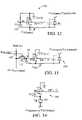
- a pixel circuit 250includes a data sampled switched current source 252 and an OLED 102 .
- Data sampled switched current source 252is similar to data sampled switched current source 120 , except that instead of having a transistor T 3 connected between ground 122 and the drain of transistor T 2 , an NMOS transistor T 5 is connected between node A and an input (e.g., a gate 254 ) of driving transistor T 2 .
- Transistor T 5is controlled by an SW signal that switches between high and low voltage levels to turn on and off, respectively, transistor T 5 .
- the SW signalis common to all pixel circuits in the array.
- the signal timings for pixel circuit 250are the same as the signal timings for pixel circuit 200 , which is shown in timing diagrams 130 of FIG. 2 .
- the SW signalis brought low ( 168 ) to disconnect transistor T 5 , thereby decoupling the gate 254 of transistor T 2 from node A, when luminance data is written into the capacitor C S . This prevents transistor T 2 from conducting while luminance data is written into the capacitor C S , allowing the voltage level of the luminance data to be accurately written into the capacitor C S .
- pixel circuit 250An advantage of pixel circuit 250 is that there is only one transistor (i.e., T 2 ) in series with the OLED 102 . Thus, pixel circuit 250 requires a lower voltage to operate than if another transistor were connected in series with the transistor T 2 . Transistor T 2 does not conduct current while data is being written to capacitor C S since the SW signal is set low during that time period and isolates the gate 254 of transistor T 2 .
- FIG. 6another example of a pixel circuit 260 is similar to pixel circuit 250 .
- a PMOS transistor T 6is used instead of the NMOS transistor T 5 .
- the SW signal in pixel circuit 250is eliminated.
- Transistor T 6is simply controlled by row line 106 .
- Pixel circuit 260may be useful when polysilicon is used to construct transistors T 1 , T 2 , and T 6 .
- a pixel circuit 300includes a double gate transistor T 7 that is used as the driving transistor for driving an OLED 102 .
- the structure of transistor T 7is shown in FIG. 8 .
- Double gate transistor T 7is a thin film transistor that has a bottom gate 302 (which functions as an accumulation gate), a top gate 304 (which functions as a depletion gate), a drain electrode 305 , and a source electrode 306 .
- bottom gate 302operates in a manner similar to the gates of transistors T 1 through T 6 .
- Bottom gate 302is formed on top of a substrate 308 .
- Substrate 308may be made of glass.
- Above the bottom gate 308is a dielectric layer 310 and an amorphous silicon layer 312 .
- Above the amorphous silicon layer 312is another dielectric layer 314 .
- a metal layer 316is deposited on top of dielectric layer 314 to form drain electrode 305 , source electrode 306 , and top gate 304 . Openings 318 in the dielectric layer 314 allow drain electrode 305 and source electrode 306 to contact the amorphous silicon layer 312 .
- bottom gate 302There is an overlap between the bottom gate 302 and the drain ( 305 ) and source ( 306 ) electrodes in the vertical direction.
- Vgsbottom gate-to-source
- Top gate 304does not overlap drain electrode 305 and source electrode 306 .
- top gate 304has a channel length that is smaller than the channel length of bottom gate 302 .
- One theory on the operation of top gate 304is that, due to the lack of overlap between the gate and the drain/source electrodes, top gate 304 appears to function similar to a depletion gate, and its operation is mostly independent of the thickness of dielectric layers 310 and 314 and the amorphous silicon layer 312 .
- Table 1summarizes the influence of the top gate-to-source voltage (Vtgs) on the drain to source current (Ids) of the transistor T 7 .
- the voltage Vbgsis the bottom gate-to-source voltage
- Vbtis the bottom gate threshold voltage
- Vttis the top gate threshold voltage.
- Vbsis a positive voltage
- Vttis a negative voltage.
- VtgsComment Vtgs ⁇ 0 Ids ⁇ (Vbgs ⁇ Vbt) 2 This applies when tran- sistor T7 operates in saturation mode. T7 has no effect on Ids. Ids ⁇ (2(Vbgs ⁇ Vbt) ⁇ Vds ⁇ This applies when tran- Vds 2 ) sistor T7 operates in non-saturation mode. T7 has no effect on Ids. Vtt ⁇ Vtgs ⁇ 0 Ids ⁇ (Vbgs ⁇ Vbt + Vtgs) 2 This applies when tran- sistor T7 operates in saturation mode. Ids is reduced by Vtgs.
- Ids⁇ (2(Vbgs ⁇ Vbt + Vtgs) ⁇ This applies when tran- Vds ⁇ Vds 2 ) sistor T7 operates in non-saturation mode. Ids is reduced by Vtgs. Vtgs ⁇ Vtt 0 Channel is pinched off
- Top gate 304has no effect on the operation of transistor T 7 if Vtgs ⁇ 0, and shuts off transistor T 7 if Vtgs ⁇ Vtt.
- Top gate 304can be fabricated from the same metal layer as the drain electrode 305 and source electrode 306 , and thus the TFT fabrication does not require any additional processing. Additional layers may exist above the TFT, such as an ITO layer, passivation layers, and vias that connection. For example, a dielectric layer may be deposited, chemically polished flat and patterned for additional via connections to subsequently deposited OLEDs for connection to the OLED anode and cathode electrodes.
- the OLEDscan be deposited below the TFTs.
- the organic TFTscan be fabricated with low temperature and would not damage the OLEDs that were previously deposited.
- Pixel circuit 300uses the same signal timings as pixel circuit 200 ( FIG. 3 ). Thus, the signal timings shown in timing diagrams 130 ( FIG. 2 ) can be used to control pixel circuit 300 . Comparing pixel circuit 300 with pixel circuit 200 , the double gate transistor T 7 replaces transistors T 2 and T 3 . Top gate 304 of transistor T 7 is controlled by an SW signal that switches between two different voltage levels. Simulations have shown that the insensitivity to threshold voltage variations of pixel circuit 300 is as good as or better than that of pixel circuit 200 .
- circuit 200due to stray capacitances between gate and drain of transistor T 2 and gate and source of transistor T 3 , there is voltage coupling between the SW signal and the capacitor C S .
- the SW signalswitches to high (or low) to turn on (or off) transistor T 3 , the voltage variations will affect the voltage level at node A, which is connected to a terminal of capacitor C S , thereby affecting the accuracy of the luminance data written into the capacitor C S .
- the voltage coupling from the SW signal to the capacitor C S in pixel circuit 300is less than the voltage coupling from the SW signal to the capacitor C S through transistor T 2 in pixel circuit 200 .
- Pixel circuit 300uses only two transistors. This design eliminates the voltage drop and electrical stress associated with the use of a third transistor (e.g., transistor T 3 of pixel circuit 200 in FIG. 3 or transistor T 5 of pixel circuit 250 in FIG. 5 ). The adverse effect on the pixel circuit due to switching of the SW signal is also reduced.
- a third transistore.g., transistor T 3 of pixel circuit 200 in FIG. 3 or transistor T 5 of pixel circuit 250 in FIG. 5 .
- Operation of pixel circuit 300may be improved by adjusting the signal voltage levels used to drive pixel circuit 300 .
- timing diagrams 400illustrate timings of signals that may be used for pixel circuit 300 to reduce OLED cathode voltage (V CA ) swings by optimizing the signal voltage levels for V CA .
- Timing diagrams 400illustrate the signal timings during a frame period t_frame, which is divided into four subperiods: an initialization subperiod 132 , a write Vt subperiod 134 , a write data subperiod 136 , and an expose subperiod 138 .
- the initialization subperiod 132spans a short interval (e.g., 10 ⁇ s) from time t 0 to t 1
- the write Vt subperiod 134spans from time t 1 to t 3
- the write data subperiod 136spans from time t 3 to t 5
- the expose subperiod 138spans from time t 5 to t 6 .
- the write Vt subperiod 134includes two intervals: the first interval from time t 1 to t 2 , and the second interval from time t 2 to t 3 .
- the signal timings of timing diagrams 400minimize the V CA voltage swings, and is designed by first determining the most negative cathode voltage allowed during time t 2 to t 3 , and then determining the cathode voltage needed during time t 1 to t 2 .
- the signal level of row line 106switches between a logical ‘1’ and a logical ‘0’.
- a logical ‘1’means that the voltage level is sufficiently high so that transistor T 1 is turned on
- a logical ‘0’means that the voltage level is sufficiently low so that transistor T 1 is turned off.
- the signal level of the SW signalalso switches between a logical ‘1’ and a logical ‘0’.
- a logical ‘0’means that the voltage level is sufficiently low so that transistor T 7 is turned off
- a logical ‘1’means that the voltage level is sufficiently high so that transistor T 1 can supply the maximum current if Vbgs of transistor T 7 is also high.
- V DATA (min)refers to the lowest voltage level for luminance data.
- V DATA (min)can be ground voltage or 0V.
- V DATA (max)refers to the voltage level for luminance data that represents the brightest luminance level of a pixel.
- the OLED cathode voltage, V CAmay have three voltage levels, represented as a function of V TH7 (min), V TH7 (max), V OLED (onset), and V OLED (max).
- V TH7 (min)refers to the initial or minimum threshold voltage of transistor T 7 .
- V TH7 (max)refers to the maximum or end-of-life threshold voltage of T 7 .
- V OLED (onset)refers to the voltage across OLED 102 at onset of luminance or conduction of the OLED. In one example, V OLED (onset) is 2V.
- V OLED (max)refers to the voltage level across OLED 102 when it is driven at its maximum luminance level.
- an equivalent circuit 500is used to explain the operation of pixel circuit 300 ( FIG. 7 ) during the initialization subperiod 132 when the signal timings in timing diagrams 400 are applied.
- Equivalent circuits 510 and 520are used to explain the operation of pixel circuit 300 during the first and second intervals, respectively, of the write Vt subperiod 134 when the signal timings in timing diagrams 400 are applied.
- equivalent pixel circuit 500shows the equivalent circuit for pixel circuit 300 during the initialization subperiod 132 (which is from time t 0 to t 1 ).
- the signal timings during the initialization subperiod 132are applied to pixel circuit 300 at the beginning of the first frame after display 700 is powered up.
- the purpose of the initialization subperiod 132is to ensure that at the beginning of the write Vt subperiod 134 , the voltage across capacitor C S is larger than V TH7 so that the transistor T 7 can conduct to discharge the capacitor C S until V CS is substantially the same as V TH7 .
- the signal timings for the initialization subperiod 132are not repeated at the beginning of subsequent frames because the leakage current of transistor T 1 tends to increase the voltage across capacitor C S .
- row line 106is set ( 402 ) to a logical ‘1’ to turn on transistor T 1 .
- Data line 104is set ( 404 ) to V DATA (min) or 0V. This combination is equivalent to grounding the bottom gate BG ( 302 ) of transistor T 7 , or setting the voltage at capacitor C S 's positive terminal 112 to 0V.
- the SW signal(applied to the top gate TG ( 304 ) of transistor T 7 ) is set ( 406 ) to logical ‘0’ so that transistor T 7 does not conduct current. This prevents current from flowing to OLED 102 so that the OLED is not turned on during the initialization subperiod 132 .
- the cathode voltage (V CA )is set ( 408 ) to a voltage level more negative than ⁇ V TH7 (max).
- OLED 102has a capacitance represented by C OLED , shown in dashed lines. Capacitor C OLED is about 10 times larger than capacitor C S .
- capacitor C OLEDwill have 0V across its terminals ( 502 and 504 ) upon power up, the voltage (V CS ) across the capacitor C S will be: V CS ⁇
- row line 106is set ( 409 ) to logical ‘0’ and the SW signal is set ( 411 ) high.
- equivalent pixel circuit 510shows the equivalent circuit for pixel circuit 300 during the interval from time t 1 to t 2 .
- V CAV TH7 (max) ⁇ V TH7 (min) ⁇ V OLED (onset).
- V CAV TH7 (max) ⁇ V TH7 (min) ⁇ V OLED (onset).
- V TH7 (max) ⁇ V TH7 (min) ⁇ V OLED (onset)may be a positive voltage. Because the cathode voltage (V CA ) is positive, current flows from source S to drain D of transistor T 7 .
- An advantage of using positive V CAis that transistor T 7 's gate-to-drain and drain-to-source voltages are reversed. Charges trapped between drain and source or between gate and drain are removed, thereby reducing degradation of transistor T 7 , reducing the variation rate of the T 7 's threshold voltage.
- the voltage at the bottom gate BG ( 302 ) of transistor T 7is: Vbg ⁇ V OLED (max) ⁇ V OLED (onset)+2 ⁇ V TH7 (max) ⁇ V TH7 (min).
- the SW signalis set ( 411 ) to logical ‘1’ to allow transistor T 7 to conduct.
- the interval between time t 1 and t 2is about 100 ⁇ s.
- an equivalent pixel circuit 520shows the equivalent circuit for pixel circuit 300 during the interval from time t 2 to t 3 .
- V CAV TH7 (min) ⁇ V OLED (onset).
- V CAV TH7 (min) ⁇ V OLED (onset).
- Eq. 10This is the most negative voltage allowable for V CA that will not cause OLED 102 to illuminate. The reason is as follows: Because node B (connected to the source electrode 305 of transistor T 7 ) will have a value of ⁇ V TH7 at the end of the write Vt subperiod 134 , the V CA voltage is set to be V OLED (onset) volts lower than ⁇ V TH7 .
- the initial voltage at the negative terminal 113 of capacitor C Sis ⁇ V TH7 (max).
- Row line 106is set ( 414 ) to a logical ‘1’ so that the bottom gate BG ( 302 ) of transistor T 7 is connected to data line 104 , which is at V DATA (min) or 0V.
- the SW signalremains at a logical ‘1’, allowing transistor T 7 to conduct current.
- T 7conducts until the voltage across capacitor C S is about V TH7 , which is transistor T 7 's present threshold voltage.
- V TH7can be any value between V TH7 (min) and V TH7 (max).
- the interval between time t 2 and t 3is about 500 ⁇ s.
- V CAis set to V TH7 (max) ⁇ V TH7 (min) ⁇ V OLED (onset) between time t 1 to t 2 so that V CA is equal to V TH7 (max) just prior to time t 2 . Reducing the interval between time t 2 and t 3 will allows more time for the write data subperiod 136 and the expose subperiod 138 .
- the SW signalis set ( 416 ) to a logical ‘0’.
- Row line 106is set ( 418 ) to logical ‘0’.
- an equivalent pixel circuit 530shows the equivalent circuit for pixel circuit 300 during the interval from time t 4 to t 4 + ⁇ t, where ⁇ t is the short time interval during which V DATA is written into the capacitors C S of a row of pixel circuits.
- ⁇ tcan be less than 10 ⁇ s.
- row line 106is set ( 420 ) to a logical ‘1’, and luminance data (V DATA ) is written into capacitor C S , which is connected to C OLED . Because capacitor C OLED is large compared to the capacitor C S , the negative terminal 113 of capacitor C S is maintained at about ⁇ V TH7 while V DATA , which is a positive voltage, is written onto the positive terminal 112 of capacitor C S .
- Row line 106is set ( 422 ) to a logical ‘0’ at time t 4 + ⁇ t. During time t 4 to t 5 , the SW signal remains at logical ‘0’ so that transistor T 7 does not conduct when V DATA is written into capacitor C S .
- the capacitor C OLEDis finite, and is about ten times larger than the capacitor C S .
- data line 104having a voltage level V DATA
- OLED 102is charged as well, so the data voltage (V DATA ) falls across both capacitors C S and C OLED .
- V DATAdata voltage
- an equivalent pixel circuit 540shows the equivalent circuit for pixel circuit 300 during the interval from time t 5 to t 6 .
- the SW signalis set ( 426 ) to a logical ‘1’, turning on transistor T 7 , causing current I to flow from transistor T 7 to OLED 102 .
- OLEDilluminates at a luminance level proportional to the current I, which is proportional to V DATA 2 , and is almost independent of the threshold voltage of transistor T 7 .
- Transistor T 7operates in the saturation region because its drain-to-source voltage is greater than its gate-to-source voltage minus its threshold voltage. TFT degradation is less severe when the transistor operates in the saturation region than when it operates in the linear region.
- OLED 102illuminates until time t 6 .
- the cycle of signal timings from time t 1 to t 6is repeated for successive frames.
- Passive matrix OLED displayshaving row or column cathode lines.
- the OLED cathodeis common to all pixels in active matrix OLED displays.
- the cathode voltage V CAis common to all pixels.
- Common cathode fabrication processis simpler and lower in cost since via connections to cathode are not required.
- power distributionis more efficient when a common or two dimensional cathode structure is used since power can be brought in from the top, bottom, left and right sides of the display.
- Row or column cathode distributionhas more resistance than a two dimension plane structure and are not as efficient. Cathode connection vias are not required when a common cathode is used.
- the SW signalmay also be common to all pixels (i.e., all pixel circuits have the same SW signal).
- Using a single SW signal and a single V CA voltage that are common to all pixelsallows the sequence of write Vt, write data, and expose subperiods to occur at the same time for all pixels. This simplifies the row and column driving circuits and the fabrication of the active matrix OLED array.
- the gate-to-source terminal capacitances of transistor T 1 that are connected to the positive terminal 112 of capacitor C Scan modify the voltage level of capacitor C S when row line 106 switches from a logical ‘1’ to a logical ‘0’ in the write data subperiod (at time t 4 + ⁇ t).
- the voltage across capacitor C Scan also be modified when V CA changes at the beginning of the expose subperiod (at time t 5 ) due to transistor T 1 's gate-to-source capacitance and T 7 bottom gate to drain capacitance.
- the voltage errors in V CS due to couplingmay be as large as 2V.
- One way to reduce voltage couplingis to reduce the width of thin film transistors T 7 and T 1 to reduce T 7 's bottom gate-to-drain and T 1 's gate-to-source capacitances.
- Using a larger data voltage rangewill allow reduction in transistor T 7 's width (because with a higher Vgs, which is equal to V DATA +V TH7 , the same current I can be achieve with a smaller channel width), but may require an increase in transistor T 1 's width (because a larger channel width for transistor T 1 is needed to charge capacitor C S to the higher data voltage level within ⁇ t).
- the storage capacitor voltage (V CS )is reduced due to row line switching, i.e., due to coupling from gate-to-source stray capacitance Cgs of transistor T 1 as row line 106 is switched from a logical ‘1’ to a logical ‘0’.
- This reduction of V CSis referred to as “row line switching coupling.”
- the amount of voltage reductionis
- V ROW (‘1’) and V ROW (‘0’)are the row line voltages at logical ‘1’ and ‘0’, respectively;
- Cgs 1 and Cgs 7are the gate-to-source capacitances of transistors T 1 and T 7 , respectively;
- capacitance Cgd 7is transistor T 7 's gate-to-drain capacitance.
- V ROW (‘1’)is designed to be greater than V DATA (max)+V TH1 (max), where V TH1 (max) is the end of life maximum threshold voltage for transistor T 1 .
- V ROW (‘0’)has a level such that V ROW (‘0’) ⁇ V OLED (max) ⁇ V DATA (min)+ V OLED (onset)+ V TH7 (min)+ V TH1 (min).
- V ROW (‘0’)is designed so that the voltage difference between row line 106 and V CA does not cause transistor T 1 to be turned on during the expose subperiod 138 .
- V CSstorage capacitor voltage
- the row line switching couplingtends to reduce the storage capacitor voltage V CS by the amount shown in Eq. 13, and the cathode voltage switching coupling tends to increase the storage capacitor voltage V CS by the amount shown in Eq. 16. It is possible to design pixel 300 circuit so that the voltage errors in V CS due to the two types of voltage couplings cancel each other. To achieve this, the V CA voltage swing is designed to be about Cgs 1 /(Cgs 1 +Cgd 7 ) of the row line voltage swing.
- V CA voltage swingFor example, if transistors T 1 and T 7 have about the same size (i.e., same widths and lengths), Cgs 1 ⁇ Cgd 7 , thus the row line voltage swing needs to be about twice the amount of the V CA voltage swing.
- the minimum allowable V CA voltage swingis V DATA (max) ⁇ V TH7 (min)+V OLED (max) ⁇ V OLED (onset). (Eq. 17)
- transistor T 7 's W/L ratiois determined by V DATA (max) and the amount of OLED current needed for achieving the desired luminance range.
- Transistor T 1 's W/Lis determined by the time available for charging capacitor C S within a row ( ⁇ t).
- transistor T 1 's W/Lmay be designed to be larger than the size required to charge capacitor C S as defined by the row time.
- V CA voltageis switched among three different voltage levels, as shown in Eqs. 7, 10, and 11.
- the switching of V CA voltagecan be simplified by using an additional transistor to directly control the OLED anode voltage.
- an example of a pixel circuit 550is similar to pixel circuit 300 ( FIG. 7 ), with an additional transistor T 8 connected between data line 104 and the negative terminal 113 of capacitor C S .
- Transistor T 8is controlled by an “RS” signal.
- timing diagrams 560show timings of signals that are used to drive pixel circuit 550 .
- Timing diagrams 560show signal timings during a frame time t_frame, which is divided into a write Vt subperiod 134 , a write data subperiod 136 , and an expose subperiod 138 .
- the write Vt subperiod 134spans from time t 0 to t 1
- the write data subperiod 136spans from time t 2 to t 4
- the expose subperiod 138spans from time t 4 to t 5 .
- an initialization subperiodis omitted in timing diagrams 560 .
- the RS signalis set ( 562 ) to a logical ‘1’, and data line 104 is set ( 564 ) to ⁇ V TH7 (max).
- Thisturns on transistor T 8 , causing anode 114 of OLED 102 to be set to the data line voltage, ⁇ V TH7 (max).
- the RS signalis set ( 566 ) to a logical ‘0’, while row line 106 is set ( 568 ) to a logical ‘1’, and data line 104 is set ( 570 ) to 0V.
- Thisturns on transistor T 1 , causing the positive terminal 112 of capacitor C S to be set to the data line voltage level, 0V.
- the write Vt subperiod 134 in timing diagrams 560can be made shorter than the write Vt subperiod 134 of timing diagrams 400 .
- the second and third steps of write Vt subperiods 134 in timing diagrams 400are combined into one step in timing diagrams 560 . Because V CA does not have to go above ⁇ V TH7 (min) ⁇ V OLED (onset), the V CA voltage swing can be reduced, thereby reducing the amount of cathode voltage switching coupling.
- a capacitor C Cmay be connected between the top gate TG ( 304 ) and the source electrode 305 of transistor T 7 . Because the SW signal is switched from logical ‘0’ to ‘1’ at the beginning of the expose subperiod 138 , the voltage coupling from top gate TG ( 304 ) to the anode 114 of OLED 102 through capacitor C C tends to increase the OLED anode voltage, thereby helping to cancel out the effects of cathode voltage switching coupling.
- the width of transistor T 1can be made smaller, and the voltage difference between logical ‘1’ and ‘0’ states for row line 106 can be reduced.
- the SW signalcan switch to a wider range of voltages above transistor T 7 's source voltage without affecting transistor T 7 's operating characteristics.
- the drain of transistor T 8can be connected to a separate control voltage.
- an example of a pixel circuit 560includes a transistor T 8 with its drain 562 connected to a control voltage V A .
- the control voltage V Ais fixed at ⁇ V TH7 (max), and may be common to all pixels in the display 700 .
- timing diagrams 570show the signal timings for pixel circuit 560 .
- the voltage across capacitor C Sis set to V TH7 (max).
- the RS signalis set ( 574 ) to logical ‘0’.
- Transistor T 7charges capacitor C S until the voltage across C S is equal to V TH7 , the current threshold voltage of transistor T 7 .
- row line 106is set ( 578 ) to logical ‘0’ to decouple capacitor C S from data line 104 .
- the data drivers 712 for driving data line 104may have a ground voltage level that is different from the ground voltage level of the other circuits in the display 700 . If the cathode voltage switching coupling (which tends to reduce V CS , the voltage across capacitor C S ) is larger than the row line switching coupling (which tends to increase V CS ), the voltage level of data line 104 may be shifted lower so as to compensate for the cathode voltage switching coupling.
- Another alternativeis to raise the ground terminal and the V CA voltage levels used by the pixel circuits relative to the voltage range of data line 104 by an amount equal to the voltage error in V CS due to voltage coupling.
- the voltage level of data line 104 during the write Vt subperiodis set to 0V or to the coupling voltage error, and not to V DATA (min).
- the simulation conditionsare such that a maximum average luminance of 300 cd/m 2 was obtained.
- a circuit simulatorthat is similar to SPICE was used to obtain transient responses for multiple frame periods.
- the data line voltageswere incremented in 1.25V or 2.5V steps over a 0 to 10V range.
- the OLED model used in the simulationhas a luminous efficiency of 4 cd/A and achieves 500 cd/m 2 at a forward voltage of about 7V.
- the turnoff and reverse bias currentsare low enough so as not to effect circuit operation.
- a transistor model for typical amorphous NMOS transistors having an initial threshold voltage (Vti) of 2.5Vwas used in the simulations.
- the transistor channel length for all transistorswere 8 microns.
- the channel width of transistor T 1was 48 microns in pixel circuits 100 , 200 , and 250 .
- the channel widths of transistors T 2 , T 3 , and T 5were 64, 48 and 48 microns, respectively.
- Capacitor C Swas 500 fF.
- the duration of the row line pulse ⁇ t during the write data subperiodwas about 10 microseconds.
- a graph 600shows normalized luminance as a function of data voltage (V DATA ) on data line 104 for a pixel circuit 610 (shown in FIG. 20 ).
- Pixel circuit 610has the same configuration as pixel circuit 100 ( FIG. 1 ), except that the drain of transistor T 2 is connected to +10V, and V CA is maintained at a constant voltage ⁇ 4.5V.
- Graph 600was obtained by simulating the circuit for multiple frame periods, but using only the signal timings in the write data and expose subperiods in timing diagram 130 ( FIG. 2 ). This represents using pixel circuit 100 by writing luminance data into the capacitor C S without threshold voltage correction.
- Line 602represents the normalized luminance as a function of data voltage (V DATA ) when the threshold voltage (V TH2 ) of transistor T 2 is at an initial value Vti.
- a graph 620shows normalized luminance of the pixel circuit 100 using the signal timing in timing diagram 130 ( FIG. 2 ).
- threshold voltage correctionwas used.
- Line 622represents the normalized luminance as a function of data voltage (V DATA ) when the threshold voltage (V TH2 ) of transistor T 2 is at the initial value Vti.
- Lines 624 , 626 , and 628show the decreases in luminance as the threshold voltage of transistor T 2 increases by 1V, 2V, and 5V, respectively.
- a graph 630shows the normalized luminance of the pixel circuit 200 in FIG. 3 that uses a data sampled switched current source 202 .
- Threshold voltage correctionis applied by using the signal timings in timing diagrams 130 ( FIG. 2 ).
- the luminancevaries little when the threshold voltage of transistor T 2 increases 2V.
- a graph 640shows a comparison of the luminance differences induced by a 1V threshold voltage variation for different pixel circuits and signal timings.
- Lines 642 and 644show the luminance differences for pixel circuits 610 and 100 , respectively, when the threshold voltage of transistor T 2 varies by 1V.
- threshold voltage correctionwas not used.
- threshold voltage correctionwas used; i.e., the signal timings in timing diagrams 130 (including the write Vt subperiod 134 ) were used.
- Line 646shows the luminance differences for pixel circuit 200 when the threshold voltage of transistor T 2 varies by 1V. The signal timings in timing diagrams 130 was used.
- a graph 650compares the luminance differences induced by a 5V threshold voltage variation.
- Lines 652 , 654 , and 656show data that were obtained under conditions similar to those for lines 642 , 644 , and 646 , respectively, but with a 5V threshold voltage difference instead of a 1V difference.
- Graphs 640 and 650show that the luminance variations for pixel circuit 200 is less than pixel circuit 100 with threshold voltage correction, which in turn has less luminance variations than pixel circuit 100 without threshold voltage correction.
- a graph 660shows luminance values as a function of data voltage for pixel circuit 250 ( FIG. 5 ).
- the widths for transistors T 1 , T 2 , and T 5 in pixel circuit 250were 48, 64, and 48 microns, respectively.
- the capacitance of capacitor C Swas 500 fF.
- Line 662shows the luminance as a function of data voltage when the threshold voltage of transistor T 2 is at an initial threshold voltage (Vti) of 2.5V.
- Lines 664 , 666 , and 668show the relationships between the luminance level and the data voltage (V DATA ) when the threshold voltage of transistor T 2 increase by 1V, 2V, and 5V, respectively.
- a comparison of line 668 with line 628 ( FIG. 21 ) and line 632 ( FIG. 22 )shows that the luminance variations of pixel circuit 250 is less than those of pixel circuit 100 , but greater than those of pixel circuit 200 for data voltages greater than 2V.
- a graph 670shows luminance variations in relation to changes in the threshold voltage of the driving transistor T 2 of pixel circuit 250 ( FIG. 5 ).
- Lines 672 , 674 , and 676show the luminance variations as a function of data voltage when the threshold voltage of transistor T 2 increases 1V, 2V, and 5V, respectively, from the initial threshold voltage.
- a graph 680shows luminance variations in relation to changes in the threshold voltage of the driving transistor T 2 of pixel circuit 200 ( FIG. 3 ).
- Lines 682 , 684 , and 686show the luminance variations as a function of data voltage when the threshold voltage of transistor T 2 increases 1V, 2V, and 5V, respectively, from the initial threshold voltage.
- the luminance differences for pixel circuit 200is greater than pixel circuit 250 when the data voltage is smaller (about less than 1V).
- the luminance differences for pixel circuit 200is less than pixel circuit 250 when the data voltage is larger (about greater than 2V).
- An advantage of using the pixel circuits described aboveis that because non-data control signals (e.g., the SW and V CA signals) can be common to all pixels in the display, standard commercial off the shelf LCD row and column drivers can be used. This reduces the cost of developing a new active matrix OLED display.
- non-data control signalse.g., the SW and V CA signals
- an active matrix display 700includes a pixel circuit array 702 that has rows and columns of pixel circuits, such as those shown in FIGS. 1 , 3 - 7 , 15 , and 17 .
- the OLEDs of pixel circuit array 702form a viewing area 704 (enclosed in a thick line) of the active matrix display 700 .
- Pixel circuits of array 702are connected to row lines 706 and data lines 708 .
- Row lines 706are controlled by row drivers 710
- data lines 708are controlled by data drivers 712 .
- a display controller 720generates and sends timing signals to the row drivers 710 through a bus 714 .
- Display controller 720generates and sends data signals and timing signals to data drivers 712 through a bus 726 .
- Display controller 720is designed to be fast enough to write data into the pixel circuits of array 702 in about half of a frame time (one frame ⁇ 16.67 ms).
- Row drivers 710 and data drivers 712can use commercially available LCD drivers.
- Display controller 720includes an auxiliary signal circuit 722 that generates SW and RS (not shown) control signals and a cathode voltage (V CA ) control signal.
- the V CA signalis connected to the cathode of the OLEDs in the pixel circuits of array 702 .
- the SW control signalis used for the pixel circuits shown in FIGS. 3-5 , 7 , 15 , and 17 .
- the auxiliary signal circuit 722generates the SW and V CA signals according to the timing diagrams shown in FIG. 2 , 9 , 16 , or 18 , depending on the type of pixel circuits used in pixel circuit array 702 .
- Auxiliary signal circuit 722has three DC voltage supply connections 724 that receive voltage signals V 1 , V 2 , and V 3 .
- the voltage signals V 1 , V 2 , and V 3supply the different voltage levels of the SW and V CA signals.
- the SW and RS (not shown) signalscan be distributed throughout the pixel circuit array 702 by using a column line (e.g., 718 ) for each column of pixel circuits.
- the SW signal distribution wiringmay be incorporated on the active matrix backplane with a single external connection.
- the V CA signalis distributed to the pixel circuits of array 702 by using a row line (or column line) for each row (or column) of pixel circuits.
- the V CA signalcan be distributed to all pixel circuits in array 702 by using a single sheet of indium tin oxide (ITO) covering the viewing area 704 of the OLED layer having external edge connections. The cathode of each OLED is thus connected to the ITO sheet, which is connected to display controller 720 through the external edge connections.
- ITOindium tin oxide
- a ground reference voltage 730is connected to the pixel circuits in array 702 by using a row line (e.g., 732 ) for each row of pixel circuits.
- the ground voltage distribution wiringcan be incorporated on the active matrix backplane with one or more external connections.
- a pixel area 734(enclosed in dashed lines) in the viewing area 704 includes an area surrounded by adjacent row lines (or ground lines) and adjacent data lines (or SW signal lines).
- transistors T 1 -T 8were described as thin film transistors and fabricated using amorphous silicon or polysilicon. Other types of transistors, such as those made of organic semiconductors, can also be used for transistors T 1 -T 8 .
- the transistors T 1 -T 3 and T 4 -T 8were described as NMOS transistors, while transistor T 4 was described as a PMOS transistor.
- the transistors T 1 -T 3 and T 4 -T 8can be PMOS transistors, and transistor T 4 can be an NMOS transistor.
- the control signals and the data signalsmay be adjusted accordingly.
- a display including the pixel circuits discussed abovemay be used in many applications. Examples are computer displays, cell phone displays, head mount displays, televisions, hand held device displays, and electronic billboards.
- the displaymay have a single color or multiple colors.
- the pixel circuitsdo not necessarily have to be arranged in a matrix of columns and rows, but may be arranged in any manner depending on application. For example, even-number rows of pixels may be offset from odd-number rows of pixels.
- the pixel circuitsmay be fabricated on a rigid (e.g., glass) or flexible (e.g., plastic) substrate.
Landscapes
- Engineering & Computer Science (AREA)
- Physics & Mathematics (AREA)
- Computer Hardware Design (AREA)
- General Physics & Mathematics (AREA)
- Theoretical Computer Science (AREA)
- Control Of Indicators Other Than Cathode Ray Tubes (AREA)
- Electroluminescent Light Sources (AREA)
- Control Of El Displays (AREA)
Abstract
Description
I∝(0.97×VDATA+VTH2−VTH2)2=(0.97×VDATA)2. (Eq. 1)
The current I causes
where VROW(high) is the logic high voltage level applied to row
where VSW(high) and VSW(low) are the logic high and low voltage levels, respectively, that are applied to the SW signal, Cgs3 is the gate-to-source capacitance of transistor T3, and Cgd is the gate-to-drain capacitance of transistor T2. Because the gate-to-source and gate-to-drain capacitances are proportional to the width of the transistor, it is possible to cancel out the net error by setting
where VCA(expose) and VCA(write data) are the voltage levels for VCAduring the expose and write data subperiods, respectively.
where μ represents mobility and Cox represents oxide capacitance. Because transistor T4 has a high W/L ratio, variations in the gate-to-source voltage are low, which result in less threshold voltage drift.
| TABLE 1 | ||
| Vtgs | Ids | Comment |
| Vtgs ≧ 0 | Ids~(Vbgs − Vbt)2 | This applies when tran- |
| sistor T7 operates in | ||
| saturation mode. T7 has | ||
| no effect on Ids. | ||
| Ids~(2(Vbgs − Vbt) × Vds − | This applies when tran- | |
| Vds2) | sistor T7 operates in | |
| non-saturation mode. T7 | ||
| has no effect on Ids. | ||
| Vtt < Vtgs < 0 | Ids~(Vbgs − Vbt + Vtgs)2 | This applies when tran- |
| sistor T7 operates in | ||
| saturation mode. Ids is | ||
| reduced by Vtgs. | ||
| Ids~(2(Vbgs − Vbt + Vtgs) × | This applies when tran- | |
| Vds − Vds2) | sistor T7 operates in | |
| non-saturation mode. Ids | ||
| is reduced by Vtgs. | ||
| Vtgs < | 0 | Channel is pinched off |
VCA=−VTH7(max)−VOLED(max). (Eq. 5)
VCS˜|VCA|=|−VOLED(max)−VTH7(max)|. (Eq. 6)
At time t1,
VCA=VTH7(max)−VTH7(min)−VOLED(onset). (Eq. 7)
The value of VCAis set to a voltage level to assure that a voltage of at least VTH7(max) is developed across capacitor COLEDat time t2. For an amorphous silicon display having a long operating lifetime, VTH7(max)−VTH7(min)−VOLED(onset) may be a positive voltage. Because the cathode voltage (VCA) is positive, current flows from source S to drain D of transistor T7.
Vbg˜VOLED(max)−VOLED(onset)+2×VTH7(max)−VTH7(min). (Eq. 8)
The SW signal is set (411) to logical ‘1’ to allow transistor T7 to conduct. Transistor T7 conducts until the
VOLED=VTH7(min)+VOLED(onset)−VTH7(max). (Eq. 9)
The interval between time t1 and t2 is about 100 μs.
VCA=−VTH7(min)−VOLED(onset). (Eq. 10)
This is the most negative voltage allowable for VCAthat will not cause
VCA=−VOLED(max)−VDATA(max). (Eq. 11)
The SW signal is set (426) to a logical ‘1’, turning on transistor T7, causing current I to flow from transistor T7 to
where VROW(‘1’) and VROW(‘0’) are the row line voltages at logical ‘1’ and ‘0’, respectively; Cgs1 and Cgs7 are the gate-to-source capacitances of transistors T1 and T7, respectively; capacitance Cgd7 is transistor T7's gate-to-drain capacitance. Assuming that COLEDis much larger than CS, Cgd7, Cgs7, and Cgs1, the equation above can be simplified as
The voltage VROW(‘1’) is designed to be greater than VDATA(max)+VTH1(max), where VTH1(max) is the end of life maximum threshold voltage for transistor T1. The voltage VROW(‘0’) has a level such that
VROW(‘0’)←VOLED(max)−VDATA(min)+VOLED(onset)+VTH7(min)+VTH1(min). (Eq. 14)
The value of VROW(‘0’) is designed so that the voltage difference between
Assuming that COLEDis much larger than CS, Cgd7, Cgs7, and Cgs1, the equation above can be approximated as
This voltage coupling is large and tends to produce off-state luminance (i.e., the
VDATA(max)−VTH7(min)+VOLED(max)−VOLED(onset). (Eq. 17)
Thus, in order to reduce the row line voltage swing while still achieving cancellation of the two types of voltage couplings, it may be necessary to increase the size of transistor T1 relative to transistor T7.
VCA=−VTH7(min)−VOLED(onset) (Eq. 18)
during the
VCA=−VTH7(min)−VOLED(onset), (Eq. 19)
and the RS signal and
Claims (24)
Priority Applications (5)
| Application Number | Priority Date | Filing Date | Title |
|---|---|---|---|
| US10/379,481US7612749B2 (en) | 2003-03-04 | 2003-03-04 | Driving circuits for displays |
| TW093104846ATWI269258B (en) | 2003-03-04 | 2004-02-25 | Driving circuits for displays |
| JP2004101268AJP5082028B2 (en) | 2003-03-04 | 2004-03-02 | Driving method of pixel circuit for display |
| CN2007101472688ACN101136173B (en) | 2003-03-04 | 2004-03-02 | Pixel circuit of display and driving method thereof |
| CNB2004100082775ACN100386788C (en) | 2003-03-04 | 2004-03-02 | Driving method of display |
Applications Claiming Priority (1)
| Application Number | Priority Date | Filing Date | Title |
|---|---|---|---|
| US10/379,481US7612749B2 (en) | 2003-03-04 | 2003-03-04 | Driving circuits for displays |
Publications (2)
| Publication Number | Publication Date |
|---|---|
| US20040174349A1 US20040174349A1 (en) | 2004-09-09 |
| US7612749B2true US7612749B2 (en) | 2009-11-03 |
Family
ID=32926688
Family Applications (1)
| Application Number | Title | Priority Date | Filing Date |
|---|---|---|---|
| US10/379,481Expired - LifetimeUS7612749B2 (en) | 2003-03-04 | 2003-03-04 | Driving circuits for displays |
Country Status (4)
| Country | Link |
|---|---|
| US (1) | US7612749B2 (en) |
| JP (1) | JP5082028B2 (en) |
| CN (2) | CN101136173B (en) |
| TW (1) | TWI269258B (en) |
Cited By (16)
| Publication number | Priority date | Publication date | Assignee | Title |
|---|---|---|---|---|
| US20050269958A1 (en)* | 2004-04-07 | 2005-12-08 | Choi Joon-Hoo | Display device and driving method thereof |
| US20070103419A1 (en)* | 2004-06-02 | 2007-05-10 | Sony Corporation | Pixel circuit, active matrix apparatus and display apparatus |
| US20070120795A1 (en)* | 2003-06-04 | 2007-05-31 | Sony Corporation | Pixel circuit, display device, and method for driving pixel circuit |
| US20080252573A1 (en)* | 2005-10-12 | 2008-10-16 | Koninklijke Philips Electronics, N.V. | Transistor Control Circuits and Control Methods, and Active Matrix Display Devices Using the Same |
| US20080284693A1 (en)* | 2005-01-26 | 2008-11-20 | Honeywell International Inc. | Active matrix organic light emitting diode display |
| US20090058771A1 (en)* | 2007-09-05 | 2009-03-05 | Sony Corporation | Method of driving organic electroluminescence emission portion |
| US20090102751A1 (en)* | 2007-10-17 | 2009-04-23 | Sony Corporation | Memory element and display device |
| US20090278781A1 (en)* | 2008-05-07 | 2009-11-12 | Art Talent Industrial Limited | Tunable current driver and operating method thereof |
| US20110001747A1 (en)* | 2007-08-10 | 2011-01-06 | Canon Kabushiki Kaisha | Thin film transistor circuit, light emitting display apparatus, and driving method thereof |
| US20130147695A1 (en)* | 2007-05-16 | 2013-06-13 | Sony Corporation | Display, method for driving display, electronic apparatus |
| US8912985B2 (en) | 2011-05-12 | 2014-12-16 | Semiconductor Energy Laboratory Co., Ltd. | Method for driving display device |
| US9262960B2 (en) | 2012-09-21 | 2016-02-16 | Chunghwa Picture Tubes, Ltd. | Organic light emitting diode display apparatus with power circuit to accelerate a voltage level |
| US9514676B2 (en) | 2013-12-12 | 2016-12-06 | Boe Technology Group Co., Ltd. | Pixel circuit and driving method thereof and display apparatus |
| US9852685B2 (en) | 2014-03-31 | 2017-12-26 | Boe Technology Group Co., Ltd. | Pixel circuit and driving method thereof, display apparatus |
| US10032798B2 (en) | 2011-09-16 | 2018-07-24 | Semiconductor Energy Laboratory Co., Ltd. | Semiconductor device, light-emitting device, and electronic device |
| US10930787B2 (en) | 2009-02-27 | 2021-02-23 | Semiconductor Energy Laboratory Co., Ltd. | Method for driving semiconductor device |
Families Citing this family (211)
| Publication number | Priority date | Publication date | Assignee | Title |
|---|---|---|---|---|
| US7569849B2 (en) | 2001-02-16 | 2009-08-04 | Ignis Innovation Inc. | Pixel driver circuit and pixel circuit having the pixel driver circuit |
| CA2419704A1 (en) | 2003-02-24 | 2004-08-24 | Ignis Innovation Inc. | Method of manufacturing a pixel with organic light-emitting diode |
| US7256758B2 (en)* | 2003-06-02 | 2007-08-14 | Au Optronics Corporation | Apparatus and method of AC driving OLED |
| US8937580B2 (en)* | 2003-08-08 | 2015-01-20 | Semiconductor Energy Laboratory Co., Ltd. | Driving method of light emitting device and light emitting device |
| CA2443206A1 (en) | 2003-09-23 | 2005-03-23 | Ignis Innovation Inc. | Amoled display backplanes - pixel driver circuits, array architecture, and external compensation |
| US7532187B2 (en)* | 2004-09-28 | 2009-05-12 | Sharp Laboratories Of America, Inc. | Dual-gate transistor display |
| US20050258867A1 (en)* | 2004-05-21 | 2005-11-24 | Seiko Epson Corporation | Electronic circuit, electro-optical device, electronic device and electronic apparatus |
| US20060044227A1 (en)* | 2004-06-18 | 2006-03-02 | Eastman Kodak Company | Selecting adjustment for OLED drive voltage |
| CA2472671A1 (en) | 2004-06-29 | 2005-12-29 | Ignis Innovation Inc. | Voltage-programming scheme for current-driven amoled displays |
| US7317433B2 (en)* | 2004-07-16 | 2008-01-08 | E.I. Du Pont De Nemours And Company | Circuit for driving an electronic component and method of operating an electronic device having the circuit |
| US7397448B2 (en)* | 2004-07-16 | 2008-07-08 | E.I. Du Pont De Nemours And Company | Circuits including parallel conduction paths and methods of operating an electronic device including parallel conduction paths |
| EP1825455A4 (en)* | 2004-11-16 | 2009-05-06 | Ignis Innovation Inc | System and driving method for active matrix light emitting device display |
| WO2006059813A1 (en)* | 2004-12-03 | 2006-06-08 | Seoul National University Industry Foundation | Picture element structure of current programming method type active matrix organic emitting diode display and driving method of data line |
| US20060118869A1 (en)* | 2004-12-03 | 2006-06-08 | Je-Hsiung Lan | Thin-film transistors and processes for forming the same |
| US7317434B2 (en)* | 2004-12-03 | 2008-01-08 | Dupont Displays, Inc. | Circuits including switches for electronic devices and methods of using the electronic devices |
| CA2490858A1 (en)* | 2004-12-07 | 2006-06-07 | Ignis Innovation Inc. | Driving method for compensated voltage-programming of amoled displays |
| US8576217B2 (en) | 2011-05-20 | 2013-11-05 | Ignis Innovation Inc. | System and methods for extraction of threshold and mobility parameters in AMOLED displays |
| TWI402790B (en) | 2004-12-15 | 2013-07-21 | Ignis Innovation Inc | Method and system for programming, calibrating and driving a light-emitting element display |
| US9799246B2 (en) | 2011-05-20 | 2017-10-24 | Ignis Innovation Inc. | System and methods for extraction of threshold and mobility parameters in AMOLED displays |
| US10013907B2 (en) | 2004-12-15 | 2018-07-03 | Ignis Innovation Inc. | Method and system for programming, calibrating and/or compensating, and driving an LED display |
| US10012678B2 (en) | 2004-12-15 | 2018-07-03 | Ignis Innovation Inc. | Method and system for programming, calibrating and/or compensating, and driving an LED display |
| CA2495726A1 (en) | 2005-01-28 | 2006-07-28 | Ignis Innovation Inc. | Locally referenced voltage programmed pixel for amoled displays |
| JP4923410B2 (en) | 2005-02-02 | 2012-04-25 | ソニー株式会社 | Pixel circuit and display device |
| JP5037795B2 (en)* | 2005-03-17 | 2012-10-03 | グローバル・オーエルイーディー・テクノロジー・リミテッド・ライアビリティ・カンパニー | Display device |
| GB0506899D0 (en)* | 2005-04-05 | 2005-05-11 | Plastic Logic Ltd | Multiple conductive layer TFT |
| TWI273544B (en)* | 2005-05-06 | 2007-02-11 | Harvatek Corp | Driving circuits and driving method of display |
| JP5355080B2 (en) | 2005-06-08 | 2013-11-27 | イグニス・イノベイション・インコーポレーテッド | Method and system for driving a light emitting device display |
| CA2518276A1 (en)* | 2005-09-13 | 2007-03-13 | Ignis Innovation Inc. | Compensation technique for luminance degradation in electro-luminance devices |
| KR101298969B1 (en)* | 2005-09-15 | 2013-08-23 | 가부시키가이샤 한도오따이 에네루기 켄큐쇼 | Semiconductor device and driving method thereof |
| JP5034208B2 (en)* | 2005-10-13 | 2012-09-26 | ソニー株式会社 | Display device and driving method of display device |
| KR101324756B1 (en) | 2005-10-18 | 2013-11-05 | 가부시키가이샤 한도오따이 에네루기 켄큐쇼 | Display device and driving method thereof |
| JP4636006B2 (en)* | 2005-11-14 | 2011-02-23 | ソニー株式会社 | Pixel circuit, driving method of pixel circuit, display device, driving method of display device, and electronic device |
| US8004477B2 (en)* | 2005-11-14 | 2011-08-23 | Sony Corporation | Display apparatus and driving method thereof |
| JP2007148129A (en)* | 2005-11-29 | 2007-06-14 | Sony Corp | Display apparatus and driving method thereof |
| JP2007148128A (en)* | 2005-11-29 | 2007-06-14 | Sony Corp | Pixel circuit |
| WO2007063814A1 (en)* | 2005-12-02 | 2007-06-07 | Semiconductor Energy Laboratory Co., Ltd. | Semiconductor device, display device, and electronic device |
| EP1793366A3 (en) | 2005-12-02 | 2009-11-04 | Semiconductor Energy Laboratory Co., Ltd. | Semiconductor device, display device, and electronic device |
| US7638416B2 (en)* | 2005-12-13 | 2009-12-29 | Versatilis Llc | Methods of making semiconductor-based electronic devices on a wire and articles that can be made using such devices |
| US7700471B2 (en)* | 2005-12-13 | 2010-04-20 | Versatilis | Methods of making semiconductor-based electronic devices on a wire and articles that can be made thereby |
| WO2007079572A1 (en) | 2006-01-09 | 2007-07-19 | Ignis Innovation Inc. | Method and system for driving an active matrix display circuit |
| US9489891B2 (en) | 2006-01-09 | 2016-11-08 | Ignis Innovation Inc. | Method and system for driving an active matrix display circuit |
| US9269322B2 (en) | 2006-01-09 | 2016-02-23 | Ignis Innovation Inc. | Method and system for driving an active matrix display circuit |
| TWI430234B (en) | 2006-04-05 | 2014-03-11 | Semiconductor Energy Lab | Semiconductor device, display device, and electronic device |
| TW200746022A (en) | 2006-04-19 | 2007-12-16 | Ignis Innovation Inc | Stable driving scheme for active matrix displays |
| JP5037858B2 (en)* | 2006-05-16 | 2012-10-03 | グローバル・オーエルイーディー・テクノロジー・リミテッド・ライアビリティ・カンパニー | Display device |
| JP4240059B2 (en)* | 2006-05-22 | 2009-03-18 | ソニー株式会社 | Display device and driving method thereof |
| KR101162553B1 (en)* | 2006-05-25 | 2012-07-05 | 엘지전자 주식회사 | Mobile communication terminal having a backlight and method of controlling the same |
| TWI336945B (en)* | 2006-06-15 | 2011-02-01 | Au Optronics Corp | Dual-gate transistor and pixel structure using the same |
| US7679586B2 (en) | 2006-06-16 | 2010-03-16 | Roger Green Stewart | Pixel circuits and methods for driving pixels |
| US8446394B2 (en)* | 2006-06-16 | 2013-05-21 | Visam Development L.L.C. | Pixel circuits and methods for driving pixels |
| US20080062090A1 (en)* | 2006-06-16 | 2008-03-13 | Roger Stewart | Pixel circuits and methods for driving pixels |
| KR101245218B1 (en)* | 2006-06-22 | 2013-03-19 | 엘지디스플레이 주식회사 | Organic light emitting diode display |
| JP4207988B2 (en)* | 2006-07-03 | 2009-01-14 | セイコーエプソン株式会社 | Light emitting device, pixel circuit driving method and driving circuit |
| JP4984715B2 (en) | 2006-07-27 | 2012-07-25 | ソニー株式会社 | Display device driving method and display element driving method |
| JP5114889B2 (en)* | 2006-07-27 | 2013-01-09 | ソニー株式会社 | Display element, display element drive method, display device, and display device drive method |
| CA2556961A1 (en) | 2006-08-15 | 2008-02-15 | Ignis Innovation Inc. | Oled compensation technique based on oled capacitance |
| KR100805596B1 (en)* | 2006-08-24 | 2008-02-20 | 삼성에스디아이 주식회사 | Organic light emitting display |
| TWI356387B (en)* | 2006-10-16 | 2012-01-11 | Au Optronics Corp | Modulation of the common voltage and controlling m |
| TWI442368B (en)* | 2006-10-26 | 2014-06-21 | Semiconductor Energy Lab | Electronic device, display device, and semiconductor device, and driving method thereof |
| JP2008158378A (en)* | 2006-12-26 | 2008-07-10 | Sony Corp | Display device and method of driving the same |
| JP2008164796A (en) | 2006-12-27 | 2008-07-17 | Sony Corp | Pixel circuit and display device and driving method thereof |
| JP2008191296A (en)* | 2007-02-02 | 2008-08-21 | Sony Corp | Display device, driving method of display device and electronic equipment |
| JP2008233502A (en)* | 2007-03-20 | 2008-10-02 | Sony Corp | Driving method of organic electroluminescence light emission part |
| JP2008233501A (en)* | 2007-03-20 | 2008-10-02 | Sony Corp | Driving method of organic electroluminescence light emitting unit |
| JP5343325B2 (en)* | 2007-04-12 | 2013-11-13 | ソニー株式会社 | Self-luminous display panel driving method, self-luminous display panel, and electronic device |
| KR100878066B1 (en)* | 2007-05-25 | 2009-01-13 | 재단법인서울대학교산학협력재단 | Flat panel display |
| TWI444967B (en) | 2007-06-15 | 2014-07-11 | Panasonic Corp | Image display device |
| JP2008310128A (en)* | 2007-06-15 | 2008-12-25 | Sony Corp | Display device, display device driving method, and electronic apparatus |
| KR101526475B1 (en) | 2007-06-29 | 2015-06-05 | 가부시키가이샤 한도오따이 에네루기 켄큐쇼 | Display device and driving method thereof |
| JP2009031620A (en)* | 2007-07-30 | 2009-02-12 | Sony Corp | Display device and driving method of display device |
| JP5157317B2 (en)* | 2007-08-21 | 2013-03-06 | ソニー株式会社 | Method for driving organic electroluminescence light emitting unit and organic electroluminescence display device |
| JP2009104013A (en)* | 2007-10-25 | 2009-05-14 | Sony Corp | Display device, driving method thereof, and electronic apparatus |
| JP5256691B2 (en)* | 2007-10-29 | 2013-08-07 | ソニー株式会社 | Display device and electronic device |
| JP4978435B2 (en)* | 2007-11-14 | 2012-07-18 | ソニー株式会社 | Display device, display device driving method, and electronic apparatus |
| JP5186888B2 (en)* | 2007-11-14 | 2013-04-24 | ソニー株式会社 | Display device, driving method thereof, and electronic apparatus |
| JP2009128404A (en)* | 2007-11-20 | 2009-06-11 | Sony Corp | Display device, driving method of display device, and electronic equipment |
| JP5119889B2 (en)* | 2007-11-26 | 2013-01-16 | ソニー株式会社 | Display device, driving method thereof, and electronic apparatus |
| JP4591511B2 (en)* | 2008-01-15 | 2010-12-01 | ソニー株式会社 | Display device and electronic device |
| JP5157467B2 (en) | 2008-01-18 | 2013-03-06 | ソニー株式会社 | Self-luminous display device and driving method thereof |
| JP5186950B2 (en) | 2008-02-28 | 2013-04-24 | ソニー株式会社 | EL display panel, electronic device, and driving method of EL display panel |
| JP5217500B2 (en)* | 2008-02-28 | 2013-06-19 | ソニー株式会社 | EL display panel module, EL display panel, integrated circuit device, electronic apparatus, and drive control method |
| EP2277163B1 (en)* | 2008-04-18 | 2018-11-21 | Ignis Innovation Inc. | System and driving method for light emitting device display |
| JP2009294635A (en)* | 2008-05-08 | 2009-12-17 | Sony Corp | Display device, method for driving display device thereof, and electronic equipment |
| JP2009288734A (en)* | 2008-06-02 | 2009-12-10 | Sony Corp | Image display device |
| CN101933072B (en)* | 2008-06-30 | 2013-04-24 | 松下电器产业株式会社 | Display device and control method thereof |
| JP4666016B2 (en)* | 2008-07-17 | 2011-04-06 | ソニー株式会社 | Display device, driving method thereof, and electronic apparatus |
| CA2637343A1 (en) | 2008-07-29 | 2010-01-29 | Ignis Innovation Inc. | Improving the display source driver |
| JP4544355B2 (en)* | 2008-08-04 | 2010-09-15 | ソニー株式会社 | Pixel circuit, driving method thereof, display device, and driving method thereof |
| JP2010049041A (en)* | 2008-08-22 | 2010-03-04 | Sony Corp | Image display device and driving method of the image display device |
| JP5650374B2 (en)* | 2008-08-29 | 2015-01-07 | エルジー ディスプレイ カンパニー リミテッド | Image display device and driving method of image display device |
| JP5207885B2 (en)* | 2008-09-03 | 2013-06-12 | キヤノン株式会社 | Pixel circuit, light emitting display device and driving method thereof |
| US7872506B2 (en)* | 2008-11-04 | 2011-01-18 | Au Optronics Corporation | Gate driver and method for making same |
| US9370075B2 (en) | 2008-12-09 | 2016-06-14 | Ignis Innovation Inc. | System and method for fast compensation programming of pixels in a display |
| JP2010145578A (en)* | 2008-12-17 | 2010-07-01 | Sony Corp | Display device, method of driving display device, and electronic apparatus |
| JP4930547B2 (en)* | 2009-05-25 | 2012-05-16 | ソニー株式会社 | Pixel circuit and driving method of pixel circuit |
| US9311859B2 (en) | 2009-11-30 | 2016-04-12 | Ignis Innovation Inc. | Resetting cycle for aging compensation in AMOLED displays |
| US10319307B2 (en) | 2009-06-16 | 2019-06-11 | Ignis Innovation Inc. | Display system with compensation techniques and/or shared level resources |
| CA2688870A1 (en) | 2009-11-30 | 2011-05-30 | Ignis Innovation Inc. | Methode and techniques for improving display uniformity |
| US9384698B2 (en) | 2009-11-30 | 2016-07-05 | Ignis Innovation Inc. | System and methods for aging compensation in AMOLED displays |
| CA2669367A1 (en) | 2009-06-16 | 2010-12-16 | Ignis Innovation Inc | Compensation technique for color shift in displays |
| KR20110013693A (en)* | 2009-08-03 | 2011-02-10 | 삼성모바일디스플레이주식회사 | Organic electroluminescent display and driving method thereof |
| KR101056281B1 (en)* | 2009-08-03 | 2011-08-11 | 삼성모바일디스플레이주식회사 | Organic electroluminescent display and driving method thereof |
| US8497828B2 (en) | 2009-11-12 | 2013-07-30 | Ignis Innovation Inc. | Sharing switch TFTS in pixel circuits |
| KR101800038B1 (en)* | 2009-12-04 | 2017-11-21 | 가부시키가이샤 한도오따이 에네루기 켄큐쇼 | Display device |
| CA2687631A1 (en) | 2009-12-06 | 2011-06-06 | Ignis Innovation Inc | Low power driving scheme for display applications |
| TWI384756B (en)* | 2009-12-22 | 2013-02-01 | Au Optronics Corp | Shift register |
| US10089921B2 (en) | 2010-02-04 | 2018-10-02 | Ignis Innovation Inc. | System and methods for extracting correlation curves for an organic light emitting device |
| US20140313111A1 (en) | 2010-02-04 | 2014-10-23 | Ignis Innovation Inc. | System and methods for extracting correlation curves for an organic light emitting device |
| US9881532B2 (en) | 2010-02-04 | 2018-01-30 | Ignis Innovation Inc. | System and method for extracting correlation curves for an organic light emitting device |
| CA2692097A1 (en) | 2010-02-04 | 2011-08-04 | Ignis Innovation Inc. | Extracting correlation curves for light emitting device |
| CA2696778A1 (en) | 2010-03-17 | 2011-09-17 | Ignis Innovation Inc. | Lifetime, uniformity, parameter extraction methods |
| CN102439652B (en)* | 2010-04-05 | 2015-05-06 | 松下电器产业株式会社 | Organic el display device and method for controlling same |
| JP5560206B2 (en)* | 2010-04-05 | 2014-07-23 | パナソニック株式会社 | Organic EL display device and control method thereof |
| KR101152464B1 (en) | 2010-05-10 | 2012-06-01 | 삼성모바일디스플레이주식회사 | Organic Light Emitting Display Device and Driving Method Thereof |
| KR101223488B1 (en)* | 2010-05-11 | 2013-01-17 | 삼성디스플레이 주식회사 | Organic Light Emitting Display and Driving Method Thereof |
| KR101182238B1 (en)* | 2010-06-28 | 2012-09-12 | 삼성디스플레이 주식회사 | Organic Light Emitting Display and Driving Method Thereof |
| KR101645404B1 (en) | 2010-07-06 | 2016-08-04 | 삼성디스플레이 주식회사 | Organic Light Emitting Display |
| KR101452655B1 (en)* | 2010-07-12 | 2014-10-22 | 샤프 가부시키가이샤 | Display device and method for driving same |
| US8907991B2 (en) | 2010-12-02 | 2014-12-09 | Ignis Innovation Inc. | System and methods for thermal compensation in AMOLED displays |
| KR101770969B1 (en)* | 2011-01-21 | 2017-08-25 | 삼성디스플레이 주식회사 | Substrate of sensing touch and method of manufacturing the substrate |
| JP5982147B2 (en) | 2011-04-01 | 2016-08-31 | 株式会社半導体エネルギー研究所 | Light emitting device |
| US8922464B2 (en) | 2011-05-11 | 2014-12-30 | Semiconductor Energy Laboratory Co., Ltd. | Active matrix display device and driving method thereof |
| US9351368B2 (en) | 2013-03-08 | 2016-05-24 | Ignis Innovation Inc. | Pixel circuits for AMOLED displays |
| CN109272933A (en) | 2011-05-17 | 2019-01-25 | 伊格尼斯创新公司 | The method for operating display |
| US20140368491A1 (en) | 2013-03-08 | 2014-12-18 | Ignis Innovation Inc. | Pixel circuits for amoled displays |
| US9606607B2 (en) | 2011-05-17 | 2017-03-28 | Ignis Innovation Inc. | Systems and methods for display systems with dynamic power control |
| US9886899B2 (en) | 2011-05-17 | 2018-02-06 | Ignis Innovation Inc. | Pixel Circuits for AMOLED displays |
| US9530349B2 (en) | 2011-05-20 | 2016-12-27 | Ignis Innovations Inc. | Charged-based compensation and parameter extraction in AMOLED displays |
| US9466240B2 (en) | 2011-05-26 | 2016-10-11 | Ignis Innovation Inc. | Adaptive feedback system for compensating for aging pixel areas with enhanced estimation speed |
| US9773439B2 (en) | 2011-05-27 | 2017-09-26 | Ignis Innovation Inc. | Systems and methods for aging compensation in AMOLED displays |
| US9881587B2 (en) | 2011-05-28 | 2018-01-30 | Ignis Innovation Inc. | Systems and methods for operating pixels in a display to mitigate image flicker |
| KR20140051268A (en) | 2011-07-22 | 2014-04-30 | 가부시키가이샤 한도오따이 에네루기 켄큐쇼 | Light-emitting device |
| US9070775B2 (en) | 2011-08-03 | 2015-06-30 | Ignis Innovations Inc. | Thin film transistor |
| US8901579B2 (en) | 2011-08-03 | 2014-12-02 | Ignis Innovation Inc. | Organic light emitting diode and method of manufacturing |
| US8710505B2 (en) | 2011-08-05 | 2014-04-29 | Semiconductor Energy Laboratory Co., Ltd. | Semiconductor device |
| JP6050054B2 (en) | 2011-09-09 | 2016-12-21 | 株式会社半導体エネルギー研究所 | Semiconductor device |
| KR101966910B1 (en)* | 2011-11-18 | 2019-08-14 | 삼성디스플레이 주식회사 | Display device and driving method thereof |
| US10089924B2 (en) | 2011-11-29 | 2018-10-02 | Ignis Innovation Inc. | Structural and low-frequency non-uniformity compensation |
| US9385169B2 (en) | 2011-11-29 | 2016-07-05 | Ignis Innovation Inc. | Multi-functional active matrix organic light-emitting diode display |
| US9324268B2 (en) | 2013-03-15 | 2016-04-26 | Ignis Innovation Inc. | Amoled displays with multiple readout circuits |
| US8937632B2 (en) | 2012-02-03 | 2015-01-20 | Ignis Innovation Inc. | Driving system for active-matrix displays |
| KR101918185B1 (en)* | 2012-03-14 | 2018-11-14 | 삼성디스플레이 주식회사 | Method for detecting array and array detecting apparatus |
| US10043794B2 (en) | 2012-03-22 | 2018-08-07 | Semiconductor Energy Laboratory Co., Ltd. | Semiconductor device and electronic device |
| TWI588540B (en)* | 2012-05-09 | 2017-06-21 | 半導體能源研究所股份有限公司 | Display device and electronic device |
| US9747834B2 (en)* | 2012-05-11 | 2017-08-29 | Ignis Innovation Inc. | Pixel circuits including feedback capacitors and reset capacitors, and display systems therefore |
| US8922544B2 (en) | 2012-05-23 | 2014-12-30 | Ignis Innovation Inc. | Display systems with compensation for line propagation delay |
| JP6228753B2 (en) | 2012-06-01 | 2017-11-08 | 株式会社半導体エネルギー研究所 | Semiconductor device, display device, display module, and electronic device |
| TWI587261B (en) | 2012-06-01 | 2017-06-11 | 半導體能源研究所股份有限公司 | Semiconductor device and driving method of semiconductor device |
| US9336717B2 (en) | 2012-12-11 | 2016-05-10 | Ignis Innovation Inc. | Pixel circuits for AMOLED displays |
| US9786223B2 (en) | 2012-12-11 | 2017-10-10 | Ignis Innovation Inc. | Pixel circuits for AMOLED displays |
| JP5879585B2 (en)* | 2012-12-12 | 2016-03-08 | 株式会社Joled | Display device and driving method thereof |
| KR20140079685A (en)* | 2012-12-19 | 2014-06-27 | 엘지디스플레이 주식회사 | Organic light emitting diode display device and method for driving the same |
| JP2014160203A (en)* | 2013-02-20 | 2014-09-04 | Sony Corp | Display unit and driving method of the same, and electronic apparatus |
| CA2894717A1 (en)* | 2015-06-19 | 2016-12-19 | Ignis Innovation Inc. | Optoelectronic device characterization in array with shared sense line |
| US9721505B2 (en) | 2013-03-08 | 2017-08-01 | Ignis Innovation Inc. | Pixel circuits for AMOLED displays |
| EP3043338A1 (en) | 2013-03-14 | 2016-07-13 | Ignis Innovation Inc. | Re-interpolation with edge detection for extracting an aging pattern for amoled displays |
| US9952698B2 (en) | 2013-03-15 | 2018-04-24 | Ignis Innovation Inc. | Dynamic adjustment of touch resolutions on an AMOLED display |
| CN105474296B (en) | 2013-08-12 | 2017-08-18 | 伊格尼斯创新公司 | A method and device for driving a display using image data |
| JP6406926B2 (en)* | 2013-09-04 | 2018-10-17 | 株式会社半導体エネルギー研究所 | Semiconductor device |
| KR102446991B1 (en) | 2013-09-13 | 2022-09-26 | 가부시키가이샤 한도오따이 에네루기 켄큐쇼 | light emitting device |
| KR102252044B1 (en)* | 2013-12-04 | 2021-05-17 | 삼성디스플레이 주식회사 | Display divece |
| US9761170B2 (en) | 2013-12-06 | 2017-09-12 | Ignis Innovation Inc. | Correction for localized phenomena in an image array |
| US9741282B2 (en) | 2013-12-06 | 2017-08-22 | Ignis Innovation Inc. | OLED display system and method |
| US9502653B2 (en) | 2013-12-25 | 2016-11-22 | Ignis Innovation Inc. | Electrode contacts |
| KR102841877B1 (en) | 2013-12-27 | 2025-08-05 | 가부시키가이샤 한도오따이 에네루기 켄큐쇼 | Light-emitting device |
| KR102203385B1 (en)* | 2013-12-30 | 2021-01-15 | 엘지디스플레이 주식회사 | Organic Light Emitting Diode Display Device |
| CN104751777B (en) | 2013-12-31 | 2017-10-17 | 昆山工研院新型平板显示技术中心有限公司 | Image element circuit, pixel and AMOLED display device and its driving method including the pixel |
| US10607542B2 (en) | 2013-12-31 | 2020-03-31 | Kunshan New Flat Panel Display Technology Center Co., Ltd. | Pixel circuit, pixel, and AMOLED display device comprising pixel and driving method thereof |
| JP6291670B2 (en)* | 2014-01-31 | 2018-03-14 | 株式会社Joled | Display device and display method |
| US10997901B2 (en) | 2014-02-28 | 2021-05-04 | Ignis Innovation Inc. | Display system |
| US10176752B2 (en) | 2014-03-24 | 2019-01-08 | Ignis Innovation Inc. | Integrated gate driver |
| DE102015206281A1 (en) | 2014-04-08 | 2015-10-08 | Ignis Innovation Inc. | Display system with shared level resources for portable devices |
| CA2872563A1 (en) | 2014-11-28 | 2016-05-28 | Ignis Innovation Inc. | High pixel density array architecture |
| CA2873476A1 (en) | 2014-12-08 | 2016-06-08 | Ignis Innovation Inc. | Smart-pixel display architecture |
| CA2879462A1 (en) | 2015-01-23 | 2016-07-23 | Ignis Innovation Inc. | Compensation for color variation in emissive devices |
| CA2886862A1 (en) | 2015-04-01 | 2016-10-01 | Ignis Innovation Inc. | Adjusting display brightness for avoiding overheating and/or accelerated aging |
| CA2889870A1 (en) | 2015-05-04 | 2016-11-04 | Ignis Innovation Inc. | Optical feedback system |
| CA2892714A1 (en) | 2015-05-27 | 2016-11-27 | Ignis Innovation Inc | Memory bandwidth reduction in compensation system |
| CA2898282A1 (en) | 2015-07-24 | 2017-01-24 | Ignis Innovation Inc. | Hybrid calibration of current sources for current biased voltage progra mmed (cbvp) displays |
| US10373554B2 (en) | 2015-07-24 | 2019-08-06 | Ignis Innovation Inc. | Pixels and reference circuits and timing techniques |
| US10657895B2 (en) | 2015-07-24 | 2020-05-19 | Ignis Innovation Inc. | Pixels and reference circuits and timing techniques |
| CA2900170A1 (en) | 2015-08-07 | 2017-02-07 | Gholamreza Chaji | Calibration of pixel based on improved reference values |
| KR102438780B1 (en)* | 2015-08-28 | 2022-09-02 | 삼성디스플레이 주식회사 | Display device and its driving method |
| CA2908285A1 (en) | 2015-10-14 | 2017-04-14 | Ignis Innovation Inc. | Driver with multiple color pixel structure |
| CA2909813A1 (en) | 2015-10-26 | 2017-04-26 | Ignis Innovation Inc | High ppi pattern orientation |
| KR102641557B1 (en)* | 2016-06-20 | 2024-02-28 | 소니그룹주식회사 | Display devices and electronic devices |
| KR102741699B1 (en)* | 2016-08-30 | 2024-12-13 | 엘지디스플레이 주식회사 | Organic Light Emitting Display Device and Driving Method thereof |
| KR102597588B1 (en)* | 2016-11-23 | 2023-11-02 | 엘지디스플레이 주식회사 | Display device and degradation compensation method of the same |
| US10586491B2 (en) | 2016-12-06 | 2020-03-10 | Ignis Innovation Inc. | Pixel circuits for mitigation of hysteresis |
| CN108234856A (en)* | 2016-12-14 | 2018-06-29 | 天津三星电子有限公司 | A kind of acquisition method and image acquiring device of the luminance information of image |
| KR102627074B1 (en)* | 2016-12-22 | 2024-01-22 | 엘지디스플레이 주식회사 | Display element, organic light emitting display device and data driver |
| KR102775758B1 (en)* | 2017-02-24 | 2025-03-07 | 삼성디스플레이 주식회사 | Pixel and organic light emitting display device having the pixel |
| EP3367374A1 (en)* | 2017-02-28 | 2018-08-29 | IMEC vzw | An active matrix display and a method for threshold voltage compensation in an active matrix display |
| CN106710523B (en)* | 2017-03-21 | 2019-03-12 | 昆山国显光电有限公司 | The driving method of organic light emitting display |
| US10714018B2 (en) | 2017-05-17 | 2020-07-14 | Ignis Innovation Inc. | System and method for loading image correction data for displays |
| US11025899B2 (en) | 2017-08-11 | 2021-06-01 | Ignis Innovation Inc. | Optical correction systems and methods for correcting non-uniformity of emissive display devices |
| CN107767814B (en)* | 2017-11-27 | 2020-02-21 | 合肥鑫晟光电科技有限公司 | Pixel circuit, display device and dual gate drive transistor |
| US10971078B2 (en) | 2018-02-12 | 2021-04-06 | Ignis Innovation Inc. | Pixel measurement through data line |
| KR102699490B1 (en) | 2018-06-22 | 2024-08-27 | 삼성디스플레이 주식회사 | Organic light emitting diode display device |
| KR102584291B1 (en)* | 2018-08-13 | 2023-10-05 | 삼성디스플레이 주식회사 | Pixel circuit and display apparatus having the same |
| US10859872B2 (en) | 2018-08-14 | 2020-12-08 | Dell Products L.P. | Method to utilize force sensors to adjust the LCD pattern or brightness on a display |
| CN109449210B (en)* | 2018-09-19 | 2022-06-10 | 云谷(固安)科技有限公司 | Array substrate and display device |
| CN109686332B (en)* | 2019-01-24 | 2021-04-30 | 合肥鑫晟光电科技有限公司 | Compensation module, logic gate circuit, gate drive circuit and display device |
| CN110136651B (en)* | 2019-06-12 | 2021-09-17 | 京东方科技集团股份有限公司 | Array substrate, OLED display panel and display device |
| CN111261110A (en)* | 2020-03-09 | 2020-06-09 | 深圳市华星光电半导体显示技术有限公司 | AMOLED pixel driving circuit, pixel driving method and display panel |
| CN112116899B (en)* | 2020-10-12 | 2024-11-15 | 北京集创北方科技股份有限公司 | Drive and electronic equipment |
| EP4016516A1 (en)* | 2020-12-18 | 2022-06-22 | Imec VZW | Pixel circuit |
| CN113299229B (en)* | 2021-05-21 | 2022-09-30 | 京东方科技集团股份有限公司 | Display panels and display devices |
| CN115050837B (en) | 2021-12-09 | 2025-04-18 | 友达光电股份有限公司 | Semiconductor devices |
| CN116884348A (en)* | 2023-07-31 | 2023-10-13 | 武汉天马微电子有限公司 | Display panel and display device |
| US12417197B2 (en)* | 2024-01-10 | 2025-09-16 | Dell Products L.P. | System to minimize effects of ground plane noise |
Citations (25)
| Publication number | Priority date | Publication date | Assignee | Title |
|---|---|---|---|---|
| US5903246A (en) | 1997-04-04 | 1999-05-11 | Sarnoff Corporation | Circuit and method for driving an organic light emitting diode (O-LED) display |
| WO1999038148A1 (en) | 1998-01-23 | 1999-07-29 | Fed Corporation | High resolution active matrix display system on a chip with high duty cycle for full brightness |
| US5952789A (en) | 1997-04-14 | 1999-09-14 | Sarnoff Corporation | Active matrix organic light emitting diode (amoled) display pixel structure and data load/illuminate circuit therefor |
| US6023259A (en) | 1997-07-11 | 2000-02-08 | Fed Corporation | OLED active matrix using a single transistor current mode pixel design |
| US6157356A (en) | 1996-04-12 | 2000-12-05 | International Business Machines Company | Digitally driven gray scale operation of active matrix OLED displays |
| US6229506B1 (en) | 1997-04-23 | 2001-05-08 | Sarnoff Corporation | Active matrix light emitting diode pixel structure and concomitant method |
| US20010043173A1 (en) | 1997-09-04 | 2001-11-22 | Ronald Roy Troutman | Field sequential gray in active matrix led display using complementary transistor pixel circuits |
| US6479940B1 (en) | 1999-09-17 | 2002-11-12 | Pioneer Corporation | Active matrix display apparatus |
| US6518962B2 (en) | 1997-03-12 | 2003-02-11 | Seiko Epson Corporation | Pixel circuit display apparatus and electronic apparatus equipped with current driving type light-emitting device |
| US6552703B1 (en) | 1999-03-04 | 2003-04-22 | Pioneer Corporation | Display apparatus of capacitive light emitting devices |
| US20030095087A1 (en) | 2001-11-20 | 2003-05-22 | International Business Machines Corporation | Data voltage current drive amoled pixel circuit |
| US6577302B2 (en)* | 2000-03-31 | 2003-06-10 | Koninklijke Philips Electronics N.V. | Display device having current-addressed pixels |
| US6583775B1 (en)* | 1999-06-17 | 2003-06-24 | Sony Corporation | Image display apparatus |
| US6680580B1 (en)* | 2002-09-16 | 2004-01-20 | Au Optronics Corporation | Driving circuit and method for light emitting device |
| US6710548B2 (en) | 2001-02-08 | 2004-03-23 | Semiconductor Energy Laboratory Co., Ltd. | Light emitting device and electronic equipment using the same |
| US20040080474A1 (en)* | 2001-10-26 | 2004-04-29 | Hajime Kimura | Light-emitting device and driving method thereof |
| US6750833B2 (en)* | 2000-09-20 | 2004-06-15 | Seiko Epson Corporation | System and methods for providing a driving circuit for active matrix type displays |
| US6777888B2 (en)* | 2001-03-21 | 2004-08-17 | Canon Kabushiki Kaisha | Drive circuit to be used in active matrix type light-emitting element array |
| US6809710B2 (en) | 2000-01-21 | 2004-10-26 | Emagin Corporation | Gray scale pixel driver for electronic display and method of operation therefor |
| US6859193B1 (en) | 1999-07-14 | 2005-02-22 | Sony Corporation | Current drive circuit and display device using the same, pixel circuit, and drive method |
| US6861810B2 (en) | 2001-10-23 | 2005-03-01 | Fpd Systems | Organic electroluminescent display device driving method and apparatus |
| US6864637B2 (en) | 2002-07-08 | 2005-03-08 | Lg. Phillips Lcd Co., Ltd. | Organic electro luminescence device and method for driving the same |
| US6885356B2 (en) | 2000-07-18 | 2005-04-26 | Nec Electronics Corporation | Active-matrix type display device |
| US6917350B2 (en)* | 2001-01-05 | 2005-07-12 | Lg Electronics Inc. | Driving circuit of active matrix method in display device |
| US6919868B2 (en)* | 2000-07-07 | 2005-07-19 | Seiko Epson Corporation | Circuit, driver circuit, electro-optical device, organic electroluminescent display device electronic apparatus, method of controlling the current supply to a current driven element, and method for driving a circuit |
Family Cites Families (8)
| Publication number | Priority date | Publication date | Assignee | Title |
|---|---|---|---|---|
| JP4251377B2 (en)* | 1997-04-23 | 2009-04-08 | 宇東科技股▲ふん▼有限公司 | Active matrix light emitting diode pixel structure and method |
| MY124701A (en)* | 1998-10-27 | 2006-06-30 | Univ Johns Hopkins | Low cost, compressed gas fuel storage system |
| JP2001083924A (en)* | 1999-09-08 | 2001-03-30 | Matsushita Electric Ind Co Ltd | Driving circuit and driving method of current control type light emitting element |
| CN1141690C (en)* | 2000-11-28 | 2004-03-10 | 凌阳科技股份有限公司 | Constant current driving circuit with automatic clamping pre-charging function |
| JP2002351401A (en)* | 2001-03-21 | 2002-12-06 | Mitsubishi Electric Corp | Self-luminous display |
| JP3613253B2 (en)* | 2002-03-14 | 2005-01-26 | 日本電気株式会社 | Current control element drive circuit and image display device |
| JP3750616B2 (en)* | 2002-03-05 | 2006-03-01 | 日本電気株式会社 | Image display device and control method used for the image display device |
| JP4734529B2 (en)* | 2003-02-24 | 2011-07-27 | 奇美電子股▲ふん▼有限公司 | Display device |
- 2003
- 2003-03-04USUS10/379,481patent/US7612749B2/ennot_activeExpired - Lifetime
- 2004
- 2004-02-25TWTW093104846Apatent/TWI269258B/ennot_activeIP Right Cessation
- 2004-03-02CNCN2007101472688Apatent/CN101136173B/ennot_activeExpired - Fee Related
- 2004-03-02JPJP2004101268Apatent/JP5082028B2/ennot_activeExpired - Fee Related
- 2004-03-02CNCNB2004100082775Apatent/CN100386788C/ennot_activeExpired - Fee Related
Patent Citations (25)
| Publication number | Priority date | Publication date | Assignee | Title |
|---|---|---|---|---|
| US6157356A (en) | 1996-04-12 | 2000-12-05 | International Business Machines Company | Digitally driven gray scale operation of active matrix OLED displays |
| US6518962B2 (en) | 1997-03-12 | 2003-02-11 | Seiko Epson Corporation | Pixel circuit display apparatus and electronic apparatus equipped with current driving type light-emitting device |
| US5903246A (en) | 1997-04-04 | 1999-05-11 | Sarnoff Corporation | Circuit and method for driving an organic light emitting diode (O-LED) display |
| US5952789A (en) | 1997-04-14 | 1999-09-14 | Sarnoff Corporation | Active matrix organic light emitting diode (amoled) display pixel structure and data load/illuminate circuit therefor |
| US6229506B1 (en) | 1997-04-23 | 2001-05-08 | Sarnoff Corporation | Active matrix light emitting diode pixel structure and concomitant method |
| US6023259A (en) | 1997-07-11 | 2000-02-08 | Fed Corporation | OLED active matrix using a single transistor current mode pixel design |
| US20010043173A1 (en) | 1997-09-04 | 2001-11-22 | Ronald Roy Troutman | Field sequential gray in active matrix led display using complementary transistor pixel circuits |
| WO1999038148A1 (en) | 1998-01-23 | 1999-07-29 | Fed Corporation | High resolution active matrix display system on a chip with high duty cycle for full brightness |
| US6552703B1 (en) | 1999-03-04 | 2003-04-22 | Pioneer Corporation | Display apparatus of capacitive light emitting devices |
| US6583775B1 (en)* | 1999-06-17 | 2003-06-24 | Sony Corporation | Image display apparatus |
| US6859193B1 (en) | 1999-07-14 | 2005-02-22 | Sony Corporation | Current drive circuit and display device using the same, pixel circuit, and drive method |
| US6479940B1 (en) | 1999-09-17 | 2002-11-12 | Pioneer Corporation | Active matrix display apparatus |
| US6809710B2 (en) | 2000-01-21 | 2004-10-26 | Emagin Corporation | Gray scale pixel driver for electronic display and method of operation therefor |
| US6577302B2 (en)* | 2000-03-31 | 2003-06-10 | Koninklijke Philips Electronics N.V. | Display device having current-addressed pixels |
| US6919868B2 (en)* | 2000-07-07 | 2005-07-19 | Seiko Epson Corporation | Circuit, driver circuit, electro-optical device, organic electroluminescent display device electronic apparatus, method of controlling the current supply to a current driven element, and method for driving a circuit |
| US6885356B2 (en) | 2000-07-18 | 2005-04-26 | Nec Electronics Corporation | Active-matrix type display device |
| US6750833B2 (en)* | 2000-09-20 | 2004-06-15 | Seiko Epson Corporation | System and methods for providing a driving circuit for active matrix type displays |
| US6917350B2 (en)* | 2001-01-05 | 2005-07-12 | Lg Electronics Inc. | Driving circuit of active matrix method in display device |
| US6710548B2 (en) | 2001-02-08 | 2004-03-23 | Semiconductor Energy Laboratory Co., Ltd. | Light emitting device and electronic equipment using the same |
| US6777888B2 (en)* | 2001-03-21 | 2004-08-17 | Canon Kabushiki Kaisha | Drive circuit to be used in active matrix type light-emitting element array |
| US6861810B2 (en) | 2001-10-23 | 2005-03-01 | Fpd Systems | Organic electroluminescent display device driving method and apparatus |
| US20040080474A1 (en)* | 2001-10-26 | 2004-04-29 | Hajime Kimura | Light-emitting device and driving method thereof |
| US20030095087A1 (en) | 2001-11-20 | 2003-05-22 | International Business Machines Corporation | Data voltage current drive amoled pixel circuit |
| US6864637B2 (en) | 2002-07-08 | 2005-03-08 | Lg. Phillips Lcd Co., Ltd. | Organic electro luminescence device and method for driving the same |
| US6680580B1 (en)* | 2002-09-16 | 2004-01-20 | Au Optronics Corporation | Driving circuit and method for light emitting device |
Non-Patent Citations (12)
Cited By (44)
| Publication number | Priority date | Publication date | Assignee | Title |
|---|---|---|---|---|
| US7714813B2 (en)* | 2003-06-04 | 2010-05-11 | Sony Corporation | Pixel circuit, display device, and method for driving pixel circuit |
| US20070120795A1 (en)* | 2003-06-04 | 2007-05-31 | Sony Corporation | Pixel circuit, display device, and method for driving pixel circuit |
| US20050269958A1 (en)* | 2004-04-07 | 2005-12-08 | Choi Joon-Hoo | Display device and driving method thereof |
| US7773057B2 (en)* | 2004-04-07 | 2010-08-10 | Samsung Electronics Co., Ltd. | Display device and driving method thereof |
| US8823607B2 (en) | 2004-06-02 | 2014-09-02 | Sony Corporation | Pixel circuit, active matrix apparatus and display apparatus with first and second reference potentials applied to source and gate of drive transistor |
| US8441417B2 (en)* | 2004-06-02 | 2013-05-14 | Sony Corporation | Pixel circuit, active matrix apparatus and display apparatus |
| US9454928B2 (en) | 2004-06-02 | 2016-09-27 | Sony Corporation | Pixel circuit, active matrix apparatus and display apparatus with first and second reference potentials applied to source, and gate of drive transistor |
| US9454929B2 (en) | 2004-06-02 | 2016-09-27 | Sony Corporation | Pixel circuit, active matrix apparatus and display apparatus with first and second reference potentials applied to source, and gate of drive transistor |
| US10002567B2 (en) | 2004-06-02 | 2018-06-19 | Sony Corporation | Pixel circuit, active matrix apparatus and display apparatus with first and second reference potentials applied to gate and other terminal of drive transistor |
| US11183119B2 (en) | 2004-06-02 | 2021-11-23 | Sony Group Corporation | Display apparatus including pixel circuit with transistors connected to different control lines |
| US20070164962A1 (en)* | 2004-06-02 | 2007-07-19 | Sony Corporation | Pixel circuit, active matrix apparatus and display apparatus |
| US20070132694A1 (en)* | 2004-06-02 | 2007-06-14 | Sony Corporation | Pixel circuit, active matrix apparatus and display apparatus |
| US10276102B2 (en) | 2004-06-02 | 2019-04-30 | Sony Corporation | Pixel circuit, active matrix apparatus and display apparatus |
| US20070103419A1 (en)* | 2004-06-02 | 2007-05-10 | Sony Corporation | Pixel circuit, active matrix apparatus and display apparatus |
| US20080284693A1 (en)* | 2005-01-26 | 2008-11-20 | Honeywell International Inc. | Active matrix organic light emitting diode display |
| US10089927B2 (en) | 2005-01-26 | 2018-10-02 | Honeywell International Inc. | Active matrix organic light emitting diode display |
| US9489886B2 (en) | 2005-01-26 | 2016-11-08 | Honeywell International Inc. | Active matrix organic light emitting diode display |
| US20080252573A1 (en)* | 2005-10-12 | 2008-10-16 | Koninklijke Philips Electronics, N.V. | Transistor Control Circuits and Control Methods, and Active Matrix Display Devices Using the Same |
| US8344970B2 (en)* | 2005-10-12 | 2013-01-01 | Koninklijke Philips Electronics N.V. | Transistor control circuits and control methods, and active matrix display devices using the same |
| US20130147695A1 (en)* | 2007-05-16 | 2013-06-13 | Sony Corporation | Display, method for driving display, electronic apparatus |
| US9041706B2 (en)* | 2007-08-10 | 2015-05-26 | Canon Kabushiki Kaisha | Thin film transistor circuit, light emitting display apparatus, and driving method thereof |
| US20140125712A1 (en)* | 2007-08-10 | 2014-05-08 | Canon Kabushiki Kaisha | Thin film transistor circuit, light emitting display apparatus, and driving method thereof |
| US8654114B2 (en)* | 2007-08-10 | 2014-02-18 | Canon Kabushiki Kaisha | Thin film transistor circuit, light emitting display apparatus, and driving method thereof |
| US20110001747A1 (en)* | 2007-08-10 | 2011-01-06 | Canon Kabushiki Kaisha | Thin film transistor circuit, light emitting display apparatus, and driving method thereof |
| US8780022B2 (en) | 2007-09-05 | 2014-07-15 | Sony Corporation | Method of driving organic electroluminescence emission portion |
| US20090058771A1 (en)* | 2007-09-05 | 2009-03-05 | Sony Corporation | Method of driving organic electroluminescence emission portion |
| US8248334B2 (en)* | 2007-09-05 | 2012-08-21 | Sony Corporation | Method of driving organic electroluminescence emission portion |
| US8144102B2 (en)* | 2007-10-17 | 2012-03-27 | Sony Corporation | Memory element and display device |
| US20090102751A1 (en)* | 2007-10-17 | 2009-04-23 | Sony Corporation | Memory element and display device |
| US8184486B2 (en)* | 2008-05-07 | 2012-05-22 | National Tsing Hua University | Tunable current driver and operating method thereof |
| US20090278781A1 (en)* | 2008-05-07 | 2009-11-12 | Art Talent Industrial Limited | Tunable current driver and operating method thereof |
| US11387368B2 (en) | 2009-02-27 | 2022-07-12 | Semiconductor Energy Laboratory Co., Ltd. | Method for driving semiconductor device |
| US10930787B2 (en) | 2009-02-27 | 2021-02-23 | Semiconductor Energy Laboratory Co., Ltd. | Method for driving semiconductor device |
| US8912985B2 (en) | 2011-05-12 | 2014-12-16 | Semiconductor Energy Laboratory Co., Ltd. | Method for driving display device |
| US10950633B2 (en) | 2011-09-16 | 2021-03-16 | Semiconductor Energy Laboratory Co., Ltd. | Semiconductor device, light-emitting device, and electronic device |
| US10032798B2 (en) | 2011-09-16 | 2018-07-24 | Semiconductor Energy Laboratory Co., Ltd. | Semiconductor device, light-emitting device, and electronic device |
| US10622380B2 (en) | 2011-09-16 | 2020-04-14 | Semiconductor Energy Laboratory Co., Ltd. | Semiconductor device, light-emitting device, and electronic device |
| US11637129B2 (en) | 2011-09-16 | 2023-04-25 | Semiconductor Energy Laboratory Co., Ltd. | Semiconductor device, light-emitting device, and electronic device |
| US12107090B2 (en) | 2011-09-16 | 2024-10-01 | Semiconductor Energy Laboratory Co., Ltd. | Semiconductor device, light-emitting device, and electronic device |
| US9262960B2 (en) | 2012-09-21 | 2016-02-16 | Chunghwa Picture Tubes, Ltd. | Organic light emitting diode display apparatus with power circuit to accelerate a voltage level |
| US20160071462A1 (en)* | 2012-09-21 | 2016-03-10 | Chunghwa Picture Tubes, Ltd. | Organic light emitting diode display apparatus with power circuit to accelerate a voltage level |
| US9524672B2 (en)* | 2012-09-21 | 2016-12-20 | Chunghwa Picture Tubes, Ltd. | Organic light emitting diode display apparatus with power circuit to accelerate a voltage level |
| US9514676B2 (en) | 2013-12-12 | 2016-12-06 | Boe Technology Group Co., Ltd. | Pixel circuit and driving method thereof and display apparatus |
| US9852685B2 (en) | 2014-03-31 | 2017-12-26 | Boe Technology Group Co., Ltd. | Pixel circuit and driving method thereof, display apparatus |
Also Published As
| Publication number | Publication date |
|---|---|
| JP5082028B2 (en) | 2012-11-28 |
| TWI269258B (en) | 2006-12-21 |
| CN101136173A (en) | 2008-03-05 |
| JP2004295131A (en) | 2004-10-21 |
| CN101136173B (en) | 2010-04-07 |
| CN1530904A (en) | 2004-09-22 |
| TW200417985A (en) | 2004-09-16 |
| CN100386788C (en) | 2008-05-07 |
| US20040174349A1 (en) | 2004-09-09 |
Similar Documents
| Publication | Publication Date | Title |
|---|---|---|
| US7612749B2 (en) | Driving circuits for displays | |
| US12051367B2 (en) | Pixel circuit and display device | |
| US20190304360A1 (en) | Display device | |
| EP1291839B1 (en) | Circuit for and method of driving current-driven device | |
| US9984626B2 (en) | Pixel circuit for organic light emitting diode, a display device having pixel circuit and driving method of pixel circuit | |
| US9373645B2 (en) | Voltage programmed pixel circuit, display system and driving method thereof | |
| CN101449314B (en) | Circuit for controlling light-emitting elements, especially organic light-emitting diodes, and method for controlling the circuit | |
| US10283045B2 (en) | Display device | |
| KR101054804B1 (en) | Pixel circuit, display device and driving method of pixel circuit | |
| JP5665256B2 (en) | Luminescent display device | |
| CN100403377C (en) | image display device | |
| US20140204067A1 (en) | Pixel Circuits and Driving Schemes for Active Matrix Organic Light Emitting Diodes | |
| US11043170B2 (en) | Pixel circuit and driving method thereof, and display apparatus | |
| US10553159B2 (en) | Pixel circuit, display panel and display device | |
| KR20100053233A (en) | Organic electro-luminescent display device and driving method thereof | |
| US20050212448A1 (en) | Organic EL display and active matrix substrate | |
| US7573442B2 (en) | Display, active matrix substrate, and driving method | |
| EP1571643A1 (en) | Organic el display and active matrix substrate |
Legal Events
| Date | Code | Title | Description |
|---|---|---|---|
| AS | Assignment | Owner name:CHI MEI OPTOELECTRONICS CORPORATION, TAIWAN Free format text:ASSIGNMENT OF ASSIGNORS INTEREST;ASSIGNORS:LIBSCH, FRANK ROBERT;SANFORD, JAMES LAWRENCE;REEL/FRAME:014060/0157 Effective date:20030303 | |
| AS | Assignment | Owner name:KYOCERA CORPORATION, JAPAN Free format text:ASSIGNMENT OF ASSIGNORS INTEREST;ASSIGNOR:CHI MEI OPTOELCTRONICS CORPORATION;REEL/FRAME:014264/0436 Effective date:20031226 Owner name:CHI MEI OPTOELECTRONICS CORPORATION, TAIWAN Free format text:ASSIGNMENT OF ASSIGNORS INTEREST;ASSIGNOR:CHI MEI OPTOELCTRONICS CORPORATION;REEL/FRAME:014264/0436 Effective date:20031226 | |
| STCF | Information on status: patent grant | Free format text:PATENTED CASE | |
| AS | Assignment | Owner name:CHIMEI INNOLUX CORPORATION,TAIWAN Free format text:MERGER;ASSIGNOR:CHI MEI OPTOELECTRONICS CORP.;REEL/FRAME:024358/0143 Effective date:20100318 | |
| FEPP | Fee payment procedure | Free format text:PAYOR NUMBER ASSIGNED (ORIGINAL EVENT CODE: ASPN); ENTITY STATUS OF PATENT OWNER: LARGE ENTITY | |
| FPAY | Fee payment | Year of fee payment:4 | |
| AS | Assignment | Owner name:INNOLUX CORPORATION, TAIWAN Free format text:CHANGE OF NAME;ASSIGNOR:CHIMEI INNOLUX CORPORATION;REEL/FRAME:032621/0718 Effective date:20121219 | |
| AS | Assignment | Owner name:INNOLUX CORPORATION, TAIWAN Free format text:ASSIGNMENT OF ASSIGNORS INTEREST;ASSIGNOR:KYOCERA CORPORATION;REEL/FRAME:035934/0794 Effective date:20150605 | |
| FPAY | Fee payment | Year of fee payment:8 | |
| FEPP | Fee payment procedure | Free format text:MAINTENANCE FEE REMINDER MAILED (ORIGINAL EVENT CODE: REM.); ENTITY STATUS OF PATENT OWNER: LARGE ENTITY | |
| FEPP | Fee payment procedure | Free format text:11.5 YR SURCHARGE- LATE PMT W/IN 6 MO, LARGE ENTITY (ORIGINAL EVENT CODE: M1556); ENTITY STATUS OF PATENT OWNER: LARGE ENTITY | |
| MAFP | Maintenance fee payment | Free format text:PAYMENT OF MAINTENANCE FEE, 12TH YEAR, LARGE ENTITY (ORIGINAL EVENT CODE: M1553); ENTITY STATUS OF PATENT OWNER: LARGE ENTITY Year of fee payment:12 |