US7612390B2 - Heterojunction transistors including energy barriers - Google Patents
Heterojunction transistors including energy barriersDownload PDFInfo
- Publication number
- US7612390B2 US7612390B2US11/357,752US35775206AUS7612390B2US 7612390 B2US7612390 B2US 7612390B2US 35775206 AUS35775206 AUS 35775206AUS 7612390 B2US7612390 B2US 7612390B2
- Authority
- US
- United States
- Prior art keywords
- layer
- barrier
- transistor according
- heterojunction transistor
- energy barrier
- Prior art date
- Legal status (The legal status is an assumption and is not a legal conclusion. Google has not performed a legal analysis and makes no representation as to the accuracy of the status listed.)
- Expired - Lifetime, expires
Links
Images


Classifications
- H—ELECTRICITY
- H10—SEMICONDUCTOR DEVICES; ELECTRIC SOLID-STATE DEVICES NOT OTHERWISE PROVIDED FOR
- H10D—INORGANIC ELECTRIC SEMICONDUCTOR DEVICES
- H10D30/00—Field-effect transistors [FET]
- H10D30/40—FETs having zero-dimensional [0D], one-dimensional [1D] or two-dimensional [2D] charge carrier gas channels
- H10D30/47—FETs having zero-dimensional [0D], one-dimensional [1D] or two-dimensional [2D] charge carrier gas channels having 2D charge carrier gas channels, e.g. nanoribbon FETs or high electron mobility transistors [HEMT]
- H10D30/471—High electron mobility transistors [HEMT] or high hole mobility transistors [HHMT]
- H10D30/473—High electron mobility transistors [HEMT] or high hole mobility transistors [HHMT] having confinement of carriers by multiple heterojunctions, e.g. quantum well HEMT
- H10D30/4732—High electron mobility transistors [HEMT] or high hole mobility transistors [HHMT] having confinement of carriers by multiple heterojunctions, e.g. quantum well HEMT using Group III-V semiconductor material
- H10D30/4738—High electron mobility transistors [HEMT] or high hole mobility transistors [HHMT] having confinement of carriers by multiple heterojunctions, e.g. quantum well HEMT using Group III-V semiconductor material having multiple donor layers
- H—ELECTRICITY
- H10—SEMICONDUCTOR DEVICES; ELECTRIC SOLID-STATE DEVICES NOT OTHERWISE PROVIDED FOR
- H10D—INORGANIC ELECTRIC SEMICONDUCTOR DEVICES
- H10D30/00—Field-effect transistors [FET]
- H10D30/01—Manufacture or treatment
- H10D30/015—Manufacture or treatment of FETs having heterojunction interface channels or heterojunction gate electrodes, e.g. HEMT
- H—ELECTRICITY
- H10—SEMICONDUCTOR DEVICES; ELECTRIC SOLID-STATE DEVICES NOT OTHERWISE PROVIDED FOR
- H10D—INORGANIC ELECTRIC SEMICONDUCTOR DEVICES
- H10D30/00—Field-effect transistors [FET]
- H10D30/40—FETs having zero-dimensional [0D], one-dimensional [1D] or two-dimensional [2D] charge carrier gas channels
- H10D30/47—FETs having zero-dimensional [0D], one-dimensional [1D] or two-dimensional [2D] charge carrier gas channels having 2D charge carrier gas channels, e.g. nanoribbon FETs or high electron mobility transistors [HEMT]
- H10D30/471—High electron mobility transistors [HEMT] or high hole mobility transistors [HHMT]
- H10D30/473—High electron mobility transistors [HEMT] or high hole mobility transistors [HHMT] having confinement of carriers by multiple heterojunctions, e.g. quantum well HEMT
- H10D30/4732—High electron mobility transistors [HEMT] or high hole mobility transistors [HHMT] having confinement of carriers by multiple heterojunctions, e.g. quantum well HEMT using Group III-V semiconductor material
- H—ELECTRICITY
- H10—SEMICONDUCTOR DEVICES; ELECTRIC SOLID-STATE DEVICES NOT OTHERWISE PROVIDED FOR
- H10D—INORGANIC ELECTRIC SEMICONDUCTOR DEVICES
- H10D62/00—Semiconductor bodies, or regions thereof, of devices having potential barriers
- H10D62/80—Semiconductor bodies, or regions thereof, of devices having potential barriers characterised by the materials
- H10D62/85—Semiconductor bodies, or regions thereof, of devices having potential barriers characterised by the materials being Group III-V materials, e.g. GaAs
- H10D62/8503—Nitride Group III-V materials, e.g. AlN or GaN
- H—ELECTRICITY
- H10—SEMICONDUCTOR DEVICES; ELECTRIC SOLID-STATE DEVICES NOT OTHERWISE PROVIDED FOR
- H10D—INORGANIC ELECTRIC SEMICONDUCTOR DEVICES
- H10D30/00—Field-effect transistors [FET]
- H10D30/80—FETs having rectifying junction gate electrodes
- H10D30/801—FETs having heterojunction gate electrodes
- H—ELECTRICITY
- H10—SEMICONDUCTOR DEVICES; ELECTRIC SOLID-STATE DEVICES NOT OTHERWISE PROVIDED FOR
- H10D—INORGANIC ELECTRIC SEMICONDUCTOR DEVICES
- H10D62/00—Semiconductor bodies, or regions thereof, of devices having potential barriers
- H10D62/80—Semiconductor bodies, or regions thereof, of devices having potential barriers characterised by the materials
- H10D62/85—Semiconductor bodies, or regions thereof, of devices having potential barriers characterised by the materials being Group III-V materials, e.g. GaAs
- H10D62/854—Semiconductor bodies, or regions thereof, of devices having potential barriers characterised by the materials being Group III-V materials, e.g. GaAs further characterised by the dopants
Definitions
- the present inventionrelates to high frequency transistors and in particular relates to microwave field effect transistors (FETs) that incorporate nitride-based active layers.
- FETsmicrowave field effect transistors
- the present inventionrelates to transistors formed of nitride semiconductor materials that can make them suitable for high power, high temperature, and/or high frequency applications.
- Materialssuch as silicon (Si) and gallium arsenide (GaAs) have found wide application in semiconductor devices for lower power and (in the case of Si) lower frequency applications. These more common semiconductor materials may not be well suited for higher power and/or high frequency applications, however, because of their relatively small bandgaps (e.g., 1.12 eV for Si and 1.42 for GaAs at room temperature) and/or relatively small breakdown voltages.
- GaAs based HEMTshave become the standard for signal amplification in civil and military radar, handset cellular, and satellite communications.
- GaAshas a higher electron mobility (approximately 6000 cm 2 /V-s) and a lower source resistance than Si, which may allow GaAs based devices to function at higher frequencies.
- GaAshas a relatively small bandgap (1.42 eV at room temperature) and relatively small breakdown voltage, which may prevent GaAs based HEMTs from providing high power at high frequencies.
- HEMThigh electron mobility transistor
- MODFETmodulation doped field effect transistor
- HFETHeterostructure Field Effect Transistor
- the 2DEGwhich forms due to the presence of an accumulation layer in the smaller bandgap material, can contain a very high sheet electron concentration in excess of, for example, 10 13 carriers/cm 2 even though the material is nominally undoped. Additionally, electrons that originate in the wider-bandgap semiconductor transfer to the 2DEG, allowing a high electron mobility due to reduced ionized impurity scattering.
- This combination of high carrier concentration and high carrier mobilitycan give the HEMT a very large transconductance and may provide a performance advantage over metal-semiconductor field effect transistors (MESFETs) for high-frequency applications, although MESFETs continue to be suitable for certain applications based on factors such as cost and reliability.
- MESFETsmetal-semiconductor field effect transistors
- High electron mobility transistors fabricated in the gallium nitride (GaN) material systemhave the potential to generate large amounts of RF power because of the combination of material characteristics that includes the aforementioned high breakdown fields, their wide bandgaps, large conduction band offset, and/or high saturated electron drift velocity.
- polarization of GaN-based materialscontributes to the accumulation of carriers in the 2DEG region.
- GaN-based HEMTshave already been demonstrated.
- U.S. Pat. No. 6,316,793, to Sheppard et al.which is commonly assigned and is incorporated herein by reference, describes a HEMT device having a semi-insulating silicon carbide substrate, an aluminum nitride buffer layer on the substrate, an insulating gallium nitride layer on the buffer layer, an aluminum gallium nitride barrier layer on the gallium nitride layer, and a passivation layer on the aluminum gallium nitride active structure.
- GaN-based materialshave large bandgaps, and high peak and saturation electron velocity values [B. Belmont, K. Kim and M. Shur, J. Appl. Phys. 74, 1818 (1993)].
- GaN HEMTscan also have 2DEG sheet densities in excess of 10 13 /cm 2 and relatively high electron mobility (up to 2000 cm 2 /V-s) [R. Gaska, J. W. Yang, A. Osinsky, Q. Chen, M. A. Khan, A. O. Orlov, G. L. Snider and M. S. Shur, Appl. Phys. Lett., 72, 707 (1998)]. These characteristics may allow GaN HEMTs to provide high power at higher frequencies.
- a conventional GaN HEMT structure 110is illustrated in FIG. 14 .
- a channel layer 114is formed on buffer layer 113 on a substrate 112 .
- a barrier layer 116is formed on the channel layer 114 .
- a source electrode 118 and a drain electrode 120form ohmic contacts through the surface of the barrier layer 116 to the electron layer that is present at the top of the channel layer 114 .
- a gate electrode 122forms a non-ohmic contact to the surface of the barrier layer 116 .
- the channel layer 114includes GaN while barrier layer 116 includes AlGaN. Because of the presence of aluminum in the crystal lattice, AlGaN has a wider bandgap than GaN. Thus, the interface between a GaN channel layer 114 and an AlGaN barrier layer 116 forms a heterostructure or heterojunction where energy bands are deformed due to, for example, Fermi level alignment and polarization in the material.
- FIG. 15is an exemplary band diagram showing the energy levels in the device along a portion of section I-I′ of FIG. 14 .
- the barrier layer 116has a lower electron affinity (X) than the channel layer 114 , when the Fermi levels in the materials align due to charge transfer, the energy bands of the channel layer 114 are shifted upwards, while those of the barrier layer are shifted downwards.
- the conduction band E cdips below the Fermi level (Ef) in the area of the channel layer 114 that is immediately adjacent to barrier layer 116 , forming a narrow accumulation region.
- a two dimensional electron gas (2DEG) sheet charge region 115is induced in the accumulation region at the heterojunction between the channel layer 114 and the barrier layer 116 .
- the barrier layer 116is made sufficiently thin so as to be depleted of mobile carriers by the junction formed with the gate 122 and the resulting shape of the conduction band.
- the conduction and valence bands in the barrier layer 116are further distorted due to polarization effects.
- This very important property of the heterostructures in the III-Nitride systemmay be essential for the high performance of the GaN HEMT.
- the total number of free electronsis enhanced greatly by pseudomorphic strain in the barrier layer relative to the channel. Due to localized piezoelectric effects, the strain causes an enhanced electric field and a higher electron concentration than would, typically, be possible were the strain not present.
- Electrons in the 2DEG sheet charge region 115demonstrate high carrier mobility. Moreover, because the sheet charge region is extremely thin, the carriers are subject to reduced impurity scattering that may improve the device's noise characteristics.
- the source to drain conductivity of this device structureis modulated by applying a voltage to the gate electrode 122 .
- a reverse voltageis applied, the conduction band beneath the gate is elevated, with the result that the conduction band E c in the vicinity of the sheet charge region 115 becomes elevated above the Fermi level, and a portion of the sheet charge region 115 is depleted of carriers, thereby preventing or reducing the flow of current from source 118 to drain 120 .
- barrier layer 116By forming the barrier layer 116 from AlN, certain advantages can be achieved.
- Using an AlN barrier layeralso reduces the piezoelectric scattering between the layers that can limit the 2DEG mobility.
- the high lattice mismatch between AlN and GaNdictates that the thickness of the AlN layer should be less than 50 ⁇ . If the layer is thicker, the device can experience problems with its ohmic contacts, the material quality in the layer begins to degrade, the device's reliability decreases, and the material is more difficult to grow. However, a HEMT with a 50 ⁇ or less AlN layer may be susceptible to high gate leakage.
- GaN-based HEMTshave demonstrated exceptional power densities, a number of technical challenges still remain to be overcome before the devices can achieve commercial success.
- one problem that may limit the performance and lifetime of certain GaN-based HEMTsis free carrier trapping, which may occur when carriers migrate away from the 2DEG region and become trapped in a surface dielectric region or in a buffer region beneath the channel. Such trapping may result in degradation in performance and/or reliability of a device.
- the amount of confinement due to the heterobarrier(which is a function of the difference in electron affinity between a wide-bandgap layer and the narrower-bandgap channel) may not be sufficiently large to result in effective confinement.
- the polarization charges present in the materialmay reduce the confinement effect of the heterobarrier.
- nitride-based transistor devicesthe mere presence of a heterojunction alone below the channel may not be sufficient to effectively prevent carriers from migrating away from the 2DEG region into the buffer region where they can become trapped.
- the structure of a DH-HEMTprovides no additional barrier against surface trapping effects.
- the problems associated with free carrier trappingmay also affect the performance of other types of nitride field effect transistors, such as GaN-based MESFETs.
- a heterojunction transistormay include a channel layer comprising a Group III nitride, a barrier layer comprising a Group III nitride on the channel layer, and an energy barrier comprising a layer of a Group III nitride including indium on the channel layer.
- the barrier layermay have a bandgap greater than a bandgap of the channel layer, and the channel layer may be between the barrier layer and the energy barrier.
- a concentration of indium (In) in the energy barriermay be greater than a concentration of indium (In) in the channel layer.
- the channel layer and the barrier layermay cooperatively induce a two-dimensional electron gas at an interface between the channel layer and the barrier layer.
- the energy barriermay include a layer of In x Ga 1-x N (0 ⁇ x ⁇ 1), and more particularly, a layer of In x Ga 1-x N (0 ⁇ x ⁇ 1).
- a mole fraction of InN (indium nitride) in an InN/GaN alloy of the energy barriermay be at least about 1%.
- a mole fraction of InN (indium nitride) in an InN/GaN alloy of the energy barriermay be in the range of about 1% to about 50%, and more particularly in the range of about 4% to about 16%.
- the energy barriermay oppose movement of carriers away from the channel layer, and/or the energy barrier may include a quantum well. Moreover, the energy barrier may have a thickness in the range of about 1 Angstrom to about 200 Angstroms, and more particularly, in the range of about 1 Angstrom to about 100 Angstroms.
- the heterojunction transistormay also include source, drain, and gate contacts on the barrier layer such that the barrier layer is between the channel layer and the source, drain, and gate contacts, and a substrate on the energy barrier such that the energy barrier is between the substrate and the channel layer.
- the barrier layermay have a thickness in the range of about 0.1 nm to about 10 nm.
- the barrier layer and the energy barriermay be separated by a distance in the range of about 5 nm to about 30 nm, and more particularly in the range of about 5 nm to about 20 nm.
- the channel layermay include a layer of Al y Ga 1-y N (0 ⁇ y ⁇ 1)
- the barrier layermay include a layer of Al z Ga 1-z N (0 ⁇ z ⁇ 1)
- y and zmay be different.
- the heterojunction transistormay include a cap layer including a Group III nitride on the barrier layer such that the barrier layer is between the cap layer and the channel layer.
- a concentration of Ga in the cap layermay be greater than a concentration of Ga in the barrier layer.
- a concentration of Al in the barrier layermay be greater than a concentration of Al in the channel layer.
- a method of forming a heterojunction transistormay include forming an energy barrier comprising a layer of a Group III nitride including indium, forming a channel layer comprising a Group III nitride on the energy barrier, and forming a barrier layer comprising a Group III nitride on the channel layer so that the channel layer is between barrier layer and the energy barrier.
- a concentration of indium (In) in the energy barriermay be greater than a concentration of indium (In) in the channel layer, and the barrier layer may have a bandgap greater than a bandgap of the channel layer.
- the channel layer and the barrier layermay cooperatively induce a two-dimensional electron gas at an interface between the channel layer and the barrier layer.
- the energy barriermay include a layer of In x Ga 1-x N (0 ⁇ x ⁇ 1), and more particularly, a layer of In x Ga 1-x N (0 ⁇ x ⁇ 1).
- a mole fraction of InN (indium nitride) in an InN/GaN alloy of the energy barriermay be at least about 1%. More particularly, a mole fraction of InN (indium nitride) in an InN/GaN alloy of the energy barrier may be in the range of about 1% to about 50%, and more particularly, in the range of about 4% to about 16%.
- the energy barriermay oppose movement of carriers away from the channel layer, and/or the energy barrier may include a quantum well. Moreover, the energy barrier may have a thickness in the range of about 1 Angstrom to about 200 Angstrom, and more particularly, in the range of about 1 Angstrom to about 100 Angstroms.
- Forming the energy barriermay include forming the energy barrier on a substrate.
- source, drain, and gate contactsmay be formed on the barrier layer after forming the barrier layer.
- the channel layermay include a layer of Al y Ga 1-y N (0 ⁇ y ⁇ 1)
- the barrier layerinclude a layer of Al z Ga 1-z N (0 ⁇ z ⁇ 1)
- y and zmay be different.
- a cap layercomprising a Group III nitride may be formed on the barrier layer, and a concentration of Ga in the cap layer may be greater than a concentration of Ga in the barrier layer.
- a concentration of Al in the barrier layermay be greater than a concentration of Al in the channel layer.
- Forming the channel layermay include forming a first portion of the channel layer on the energy barrier at a first temperature. After forming the first portion of the channel layer, a second portion of the channel layer may be formed at a second temperature on the first portion of the channel layer wherein the first temperature is less than the second temperature.
- the first temperaturefor example, may be at least about 100 degrees C. less than the second temperature.
- the first and second portions of the channel layermay each comprise GaN.
- a heterojunction transistormay include a channel layer, a barrier layer on the channel layer, and an energy barrier on the channel layer such that the channel layer is between the barrier layer and the energy barrier.
- the barrier layer and the channel layermay cooperatively induce a two-dimensional electron gas at an interface between the channel layer and the barrier layer, and the energy barrier may oppose movement of carriers away from the channel layer.
- the energy barriermay include a quantum well.
- the channel layermay include a first layer of a Group III nitride
- the barrier layermay include a second layer of a Group III nitride
- the energy barriermay include a third layer of a Group III nitride.
- the energy barriermay include a layer of In x Ga 1-x N (0 ⁇ x ⁇ 1), and more particularly, the energy barrier may include a layer of In x Ga 1-x N (0 ⁇ x ⁇ 1).
- a mole fraction of InN (indium nitride) in an InN/GaN alloy of the energy barriermay be at least about 1%, and more particularly, in the range of about 1% to about 50%, and more particularly, in the range of about 4% to about 16%.
- the energy barriermay have a thickness in the range of about 1 Angstrom to about 200 Angstroms, and more particularly, in the range of about 1 Angstrom to about 100 Angstroms.
- the heterojunction transistormay also include source, drain, and gate contacts on the barrier layer such that the barrier layer is between the channel layer and the source, drain, and gate contacts, and the heterojunction transistor may also include a substrate on the energy barrier such that the energy barrier is between the substrate and the channel layer.
- the channel layermay include a Group III nitride
- the barrier layermay include a Group III nitride
- the barrier layermay have a bandgap greater than a bandgap of the channel layer.
- the channel layermay include a layer of Al y Ga 1-y N (0 ⁇ y ⁇ 1)
- the barrier layermay include a layer of Al z Ga 1-z N (0 ⁇ z ⁇ 1)
- y and zmay be different.
- a cap layer including a Group III nitridemay be provided on the barrier layer such that the barrier layer is between the cap layer and the channel layer, and a concentration of Ga in the cap layer may be greater than a concentration of Ga in the barrier layer.
- the barrier layermay include a Group III nitride and the channel layer may include a Group III nitride, and a concentration of Al in the barrier layer may be greater than a concentration of Al in the channel layer.
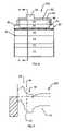
- FIG. 1is a schematic drawing showing a transistor structure according to embodiments of the present invention.
- FIG. 1Ais a schematic drawing showing a transistor structure according to further embodiments of the present invention.
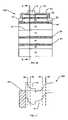
- FIG. 2is an illustrative graph showing (a) the charge density, (b) electric field and (c) electric potential within a region of the structure of FIG. 1 .
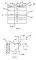
- FIG. 3is an illustrative graph of the band diagram of a region within the embodiments illustrated in FIG. 1 .
- FIG. 4is a schematic drawing showing a transistor structure according to further embodiments of the present invention.
- FIG. 5is an illustrative graph of the band diagram of a region within the embodiments illustrated in FIG. 4 .
- FIG. 6is a schematic drawing showing a transistor structure according to further embodiments of the present invention.
- FIG. 7is an illustrative graph of the band diagram of a region within the embodiments illustrated in FIG. 6 .
- FIG. 8is a schematic drawing showing a transistor structure according to further embodiments of the present invention.
- FIG. 9is an illustrative graph of the band diagram of a region within the embodiments illustrated in FIG. 8 .
- FIG. 10is a schematic drawing showing a transistor structure according to further embodiments of the present invention.
- FIG. 11is an illustrative graph of the band diagram of a region within the embodiments illustrated in FIG. 10 .
- FIG. 12is a schematic drawing showing a transistor structure according to further embodiments of the present invention.
- FIG. 13is an illustrative graph of the band diagram of a region within the embodiments illustrated in FIG. 12 .
- FIG. 14is a schematic diagram of a prior art HEMT structure.
- FIG. 15is an illustrative graph of the band diagram of a region within the structure illustrated in FIG. 14 .
- FIGS. 16-18are flowcharts illustrating operations according to further embodiments of the invention.
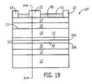
- FIG. 19is a schematic drawing showing a transistor structure according to still further embodiments of the present invention.
- FIG. 20is a table providing target parameters for HEMT structures (Sample 1 - 11 ) including InGaN energy barrier layers according to embodiments of the present invention and for comparative HEMT structures (Control 1 - 2 ) without InGaN energy barrier layers.
- FIG. 21Ais a band diagram for a HEMT without an InGaN energy barrier layer.
- FIG. 21Bis a band diagram for a HEMT including an InGaN energy barrier layer according to embodiments of the present invention.
- FIG. 22is a graph showing output resistances (Rds) for HEMTs having different estimated compositions of InGaN barrier layers according to embodiments of the present invention.
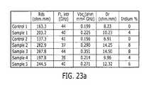
- FIG. 23 ais a table providing parameters for HEMT structures (Sample 1 - 5 corresponding to Sample 1 - 5 of FIG. 20 ) including InGaN energy barrier layers according to embodiments of the present invention, and for comparative HEMT structures (Control 1 - 2 corresponding to Control 1 - 2 of FIG. 20 ) without InGaN energy barrier layers.
- FIGS. 23 b - care graphs illustrating back-confinement values Vbc and device resistances Dr, respectively, as functions of a percentage of Indium in the InGaN layer in the structures of FIG. 23 a according to embodiments of the present invention.
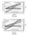
- FIGS. 24 a - binclude graphs illustrating gain, power out, and power added efficiency for control HEMT structures and for HEMT structures according to embodiments of the present invention.
- FIGS. 25 a - binclude graphs illustrating drain currents for control HEMT structures and for HEMT structures according to embodiments of the present invention.
- FIG. 26includes graphs illustrating power added efficiency, power out, and gain as functions of power in for HEMT structures according to embodiments of the present invention.
- FIG. 27includes graphs illustrating power added efficiency, power out, and gain as functions of drain-source voltage for HEMT structures according to embodiments of the present invention.
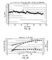
- FIG. 28includes a graph illustrating power out as a function of time for HEMT structures according to embodiments of the present invention.
- FIG. 29includes graphs illustrating power added efficiency, power out, and gain as functions of power in for HEMT structures according to embodiments of the present invention.
- references herein to a layer formed “on” a substrate or other layermay refer to the layer formed directly on the substrate or other layer or on an intervening layer or layers formed on the substrate or other layer.
- references herein to a layer formed “on” a substrate or other layermay refer to the layer formed directly on the substrate or other layer or on an intervening layer or layers formed on the substrate or other layer.
- the term “and/or”includes any and all combinations of one or more of the associated listed items.
- first, second, etc.may be used herein to describe various regions, layers, and/or sections, these regions, layers, and/or sections should not be limited by these terms. These terms are only used to distinguish one region, layer, or section from another region, layer, or section. Thus, a first region, layer, or section discussed below could be termed a second region, layer, or section, and similarly, a second without departing from the teachings of the present invention.
- Embodiments of the present inventionmay provide enhanced confinement of carriers through the inclusion of a high-field region on one or both sides of a channel.
- the electric field in the high field regionmay be generated by the transfer of charge between an electron source region and a hole source region.
- the electric field in the high field regionis directed away from the channel.
- the electric fieldopposes the movement of negatively charged electrons away from the channel.
- the direction of an electric fieldis defined by the direction of electric force acting on a positively charged particle.
- Group III nitriderefers to those semiconducting compounds formed between nitrogen and the elements in Group III of the periodic table, usually aluminum (Al), gallium (Ga), and/or indium (In).
- the termalso refers to ternary and quaternary compounds such as AlGaN and AlInGaN.
- the Group III elementscan combine with nitrogen to form binary (e.g., GaN), ternary (e.g., AlGaN, AlInN), and quaternary (e.g., AlInGaN) compounds. These compounds all have empirical formulas in which one mole of nitrogen is combined with a total of one mole of the Group III elements.
- Al x Ga 1-x Nwhere 0 ⁇ x ⁇ 1 are often used to describe them.
- the term InAlGaNmay refer to GaN, InN, AlN, AlGaN, AlInN, InGaN and/or AlInGaN unless otherwise specified or limited.
- the terms “InAlGaN”, “Group III-nitride material” and “nitride-based material”are used interchangeably throughout this specification.
- Embodiments of the present inventionare schematically illustrated as a high electron mobility transistor (HEMT) 10 in the cross-sectional view of FIG. 1 .
- the transistor 10includes a substrate 12 that may be, for example, semi-insulating silicon carbide (SiC) of the 4H polytype.
- SiCsilicon carbide
- Other silicon carbide candidate polytypes including the 2H, 3C, 6H, and 15R polytypesmay be utilized.
- the term “semi-insulating”is used descriptively in a relative sense rather than in an absolute sense.
- the silicon carbide bulk crystalmay have a resistivity equal to or higher than about 1 ⁇ 10 5 ⁇ -cm at room temperature.
- a buffer layer 13 on the substrate 12provides an appropriate crystalline transition between the substrate 12 and the remainder of the device.
- Buffer layer 13may include one or more layers of InAlGaN.
- buffer layer 13may include AlN or AlGaN.
- Silicon carbidehas a much closer crystal lattice match to Group III nitrides than does sapphire (Al 2 O 3 ), which is a very common substrate material for Group III nitride devices. The closer lattice match may result in Group III nitride films of higher quality than those generally available on sapphire.
- Silicon carbidealso has a very high thermal conductivity so that the total output power of Group III nitride devices on silicon carbide is, typically, not as limited by thermal dissipation of the substrate as in the case of the same devices formed on sapphire. Also, the availability of semi-insulating silicon carbide substrates may provide for device isolation and reduced parasitic capacitance.
- silicon carbideis the preferred substrate material
- embodiments of the present inventionmay utilize any suitable substrate, such as sapphire, aluminum nitride, aluminum gallium nitride, gallium nitride, silicon, GaAs, LGO, ZnO, LAO, InP and the like.
- an appropriate buffer layeralso may be formed.
- Suitable SiC substratesare manufactured by, for example, Cree, Inc., of Durham, N.C., the assignee of the present invention, and the methods for producing are described, for example, U.S. Pat. Nos. Re. 34,861; 4,946,547; 5,200,022; and 6,218,680, the contents of which are incorporated herein by reference in their entirety.
- techniques for epitaxial growth of Group III nitrideshave been described in, for example, U.S. Pat. Nos. 5,210,051; 5,393,993; 5,523,589; and 5,592,501, the contents of which are also incorporated herein by reference in their entirety.
- a transistor 10includes a channel layer 14 .
- the channel layer 14includes InAlGaN.
- the channel layer 14includes Al x Ga 1-x N (0 ⁇ x ⁇ 1).
- the channel layer 14includes GaN.
- the channel layer 14may be undoped and may be grown to a thickness of between about 50 and about 500 ⁇ .
- the channel layer 14may be thinner than channel layers in conventional GaN HEMT devices, which are typically greater than 500 ⁇ in thickness.
- many of the embodiments, including the embodiment of FIG. 1may be formed using N-polar or non-polar material without departing from the scope of the invention.
- a barrier layer 16is provided on the channel layer 14 .
- the barrier layer 16may be a Group III-nitride having a bandgap larger than that of the channel layer 14 . Accordingly, the barrier layer 16 may be AlGaN, AlInGaN, AlInN and/or AlN.
- the barrier layer 16may be at least about 10 nm thick, but is not so thick as to cause cracking or defect formation therein. Moreover, the barrier layer 16 should be thin enough that it is completely depleted under equilibrium conditions.
- the barrier layer 16is undoped or doped with activated donor atoms at a concentration of less than about 10 19 cm ⁇ 3 .
- the barrier layer 16may be delta-doped at a concentration of up to about 10 13 cm ⁇ 2 at a distance of about 100 ⁇ (Angstroms) from the interface between barrier layer 16 and channel layer 14 .
- the barrier layer 16includes Al x Ga 1-x N where 0 ⁇ x ⁇ 1.
- the barrier layer 16includes AlGaN with an aluminum concentration of between about 5% and about 100%. In specific embodiments of the present invention, the aluminum concentration is greater than about 10%.
- the barrier layer 16has a bandgap greater than that of the channel layer 14 .
- the barrier layermay also be provided with multiple layers as described in U.S. patent application Ser. No. 10/102,272, to Smorchkova et al., entitled “GROUP-III NITRIDE BASED HIGH ELECTRON MOBILITY TRANSISTOR (HEMT) WITH BARRIER/SPACER LAYER” and U.S. Pat. No. 6,316,793 entitled “Nitride Based Transistors on Semi-Insulating Silicon Carbide Substrates with Passivation Layer” issued Nov. 13, 2001, the disclosures of which are incorporated herein by reference as if set forth fully herein.
- embodiments of the present inventionshould not be construed as limiting the barrier layer to a single layer but may include, for example, barrier layers having combinations of InAlGaN layers having various material compositions.
- barrier layers having combinations of InAlGaN layers having various material compositionsFor example, a GaN/AlN structure may be utilized to reduce or prevent alloy scattering.
- An optional InAlGaN contact layer or cap layermay be provided on the barrier layer 16 to facilitate the formation of contacts of the transistor 10 .
- An example of such a cap layeris disclosed in U.S. application Ser. No. 09/904,333 filed Jul. 12, 2001 for “ALUMINUM GALLIUM NITRIDE/GALLIUM NITRIDE HIGH ELECTRON MOBILITY TRANSISTORS HAVING A GATE CONTACT ON A GALLIUM NITRIDE BASED CAP SEGMENT AND METHODS OF FABRICATING SAME,” which is referenced above.
- the source contact 18 , the drain contact 20 and the gate contact 22may be fabricated as described in U.S. Pat. No. 6,316,793.
- a 2DEG sheet charge region 15is induced at the interface between channel layer 14 and barrier layer 16 .
- a region 32 having a high electric fieldis provided between the channel layer 14 and the buffer layer 13 .
- the high fieldis generated by charge transfer between an electron source layer 34 and a hole source layer 30 which are spaced apart by a distance “d” which defines the thickness of the high field region 32 .
- the electron source layer 34may include a thin layer of a Group III-nitride material such as Al x Ga 1-x N (0 ⁇ x ⁇ 1) that is highly doped with donor (n-type) dopants
- the hole source layer 30may include a thin layer of a Group III-nitride material such as Al x Ga 1-x N (0 ⁇ x ⁇ 1) that is highly doped with acceptor (p-type) dopants.
- the electron source layer 34 and the hole source layer 30are spaced apart by a distance “d” that defines a high field region 32 therebetween.
- This charge transfercauses a depletion region to form between the electron source region and the hole source region.
- the charge transfermay fully deplete the electron source region and/or the hole source region.
- the depletion regionis characterized by a high electric field directed away from the channel layer 14 .
- the magnitude of the induced electric fieldis proportional to the doping levels in the electron source layer and the hole source layer.
- a built-in potentialis developed between the electron source layer and the hole source layer that is proportional to the thickness of the high field region (i.e. the distance between the electron source region and the hole source region.
- a potential barrier up to the bandgap(less the donor and acceptor ionization energies) may be formed.
- the buffer 13may be doped with deep acceptors as described in S. Heikman et al., Growth of Fe-Doped Semi-insulating GaN by Metalorganic Chemical Vapor Deposition, Appl. Phys. Let. 81, pp. 439-441 (2002).
- Specific examples of co-doped layersare provided in U.S. patent application Ser. No. 10/752,970 entitled “Co-Doping for Fermi Level Control in Semi-Insulating Group III Nitrides”, filed Jan. 7, 2004 and assigned to the assignee of the present invention, the disclosure of which is incorporated herein by reference.
- the buffercould be doped with Fe or another deep acceptor.
- FIG. 2shows illustrative graphs of charge ( FIG. 2( a )), electric field ( FIG. 2( b )) and voltage ( FIG. 2( c )) in the vicinity of a pair of thin, oppositely doped layers having high dopant concentrations.
- Graphs of band energies, voltages, electric fields and chargesuch as the graphs in FIG. 2 are not intended to be to scale, nor are they graphs of actual measurements. Rather, they are exemplary graphs that are included merely to illustrate various characteristics of the structures in question.
- the layeris characterized by a fixed positive charge from the ionized donor atoms.
- the electron source layer and hole source layerare modeled as thin, highly doped layers spaced a distance “d” apart.
- the electric field within the structureis obtained by integrating the charge density along the direction of interest. Mathematically, the electric field E is given by the following equation:
- V ⁇ ( x )- ⁇ - ⁇ x ⁇ E ⁇ ( x ) ⁇ ⁇ d x
- the electric potential in the structureis illustrated in FIG. 2( c ).
- the maximum value of the electric potentialcalled the built-in voltage and designated V bi , is reached at the edge of the hole source layer 30 . Accordingly, the distance “d” between the electron source layer and the hole source layer and the magnitude of the electric field E collectively determine the magnitude of the potential barrier provided by the high field region 32 .
- the electric field between the two sheets of chargeis then (q ⁇ P sheet )/ ⁇ where q is the elementary charge (1.602*10 ⁇ 19 C) and ⁇ is the dielectric constant of the material (about 9*8.85*10 ⁇ 14 F/cm for GaN).
- qis the elementary charge (1.602*10 ⁇ 19 C)
- ⁇is the dielectric constant of the material (about 9*8.85*10 ⁇ 14 F/cm for GaN).
- the electric fieldwould be about P sheet *(2 ⁇ 10 ⁇ 7 V-cm).
- the fieldwould be about 2 ⁇ 10 5 V/cm.
- V bid *( q*P sheet )/ ⁇
- This voltageis necessarily less than E g ⁇ E a ⁇ E d
- E gis the energy gap
- E ais the acceptor ionization energy relative to the valence band
- E dis the donor ionization energy relative to the conduction band.
- a voltage for the barriershould be chosen to be safely below E g ⁇ E a ⁇ E d .
- a 2V barriermay be an appropriate goal.
- d ⁇ P sheet ⁇ 2 ⁇ 5 ⁇ 10 6 /cm10 7 /cm
- the semiconductor crystalmay be delta doped.
- delta dopingrefers to doping a semiconductor layer with a very high density of dopants in a very thin region.
- the semiconductor crystal of Al x Ga 1-x Nmay be doped with an acceptor such as Mg or Zn at an activated concentration of about 10 18 cm ⁇ 3 for a depth of about 10 nm.
- Hole source layer 30may be doped with deep level acceptor elements such as Fe or V.
- hole source layer 30may be co-doped with deep level transition elements, such as Fe or V, along with shallow acceptor dopants, such as Zn and/or Mg.
- deep level transition elementssuch as Fe or V
- shallow acceptor dopantssuch as Zn and/or Mg.
- E ashallow acceptors with smaller activation energies E a may yield a larger maximum built-in voltage V bi .
- free acceptorscould be generated which would adversely impact device performance.
- V biit may be preferable to keep V bi fairly low and choose a dopant with a low memory effect in the growth system.
- the electron source layermay be doped with Si, Ge or O atoms.
- other forms of dopingmay be used in conjunction with thicker layers.
- doping in the layerscould be progressively graded or abrupt.
- the electron source layer and the hole source layermay be thicker or thinner than 10 nm.
- the electron source layer and hole source layermay each range in thickness from about 0.2 nm to about 100 nm. The electron source layer and the hole source layer do not have to have the same thickness or doping density.
- “d”may be less than about 0.1 ⁇ m.
- the thickness “d” of the high field region 32may range from about 10 nm to about 200 nm.
- the barriermay have a potential height of less than about 0.5V. In other embodiments, the barrier height may be about 1V or less. In still other embodiments, the barrier height may be about 2V or less. As discussed above, the limit on the barrier height is that it be less than (E g ⁇ E a ⁇ E d ).
- the electron source layermay include the 2DEG region induced at the interface of the barrier layer and the channel layer.
- the 2DEG regionshould not be fully depleted by the hole source region.
- FIG. 1AAn example of such embodiments is shown in FIG. 1A in which a hole source region 30 is formed beneath the channel layer 14 .
- the 2DEG region 15 at the interface between channel layer 14 and barrier layer 16acts as the electron source layer 34 .
- the entire channel layer 14may function as a high-field region 32 that opposes the movement of carriers away from the 2DEG region 15 .
- FIG. 3is a graph of energy level versus position (x) in portions of the transistor 10 .
- AlGaNhas a wider bandgap than GaN.
- the interface between the channel layer 14 and the barrier layer 16forms a heterostructure in which the conduction and valence bands E c and E v are offset. Charge is induced due to the piezoelectric effect and spontaneous doping.
- the conduction band E cdips below the Fermi level E f in the area of the channel layer 14 that is immediately adjacent to the barrier layer 16 . Consequently, a two dimensional electron gas (2DEG) sheet charge region is induced at the heterojunction between the channel layer 14 and the barrier layer 16 , while layer 16 is depleted of mobile carriers due to the shape of the conduction band.
- 2DEGtwo dimensional electron gas
- the conductivity of this regionis modulated by applying a voltage to the gate electrode 22 .
- a reverse voltageis applied, the conduction band in the vicinity of conduction layer 15 is elevated above the Fermi level, and a portion of the conduction layer 15 is depleted of carriers, thereby preventing the flow of current from the source 18 to the drain 20 .
- an energy barrieris formed by inserting the electron source layer 34 and the hole source layer 30 between the channel layer 14 and the buffer layer 13 .
- the electron source layer 34 and the hole source layer 30are spaced apart by a distance “d” which defines a region 32 having a high electric field.
- the slope of the energy bands within the region 32is directly related to the strength of the electric field in this region.
- the large slope of the conduction band Ec within the high field region 32presents a large potential barrier that opposes the movement of electrons from the channel layer 14 toward the buffer layer 13 . More specifically, the potential barrier created by the high field region 32 tends to cause electrons in the 2DEG region not to migrate into the buffer region where they could become trapped or become less susceptible to influence by a gate voltage.
- structure 10 A of FIG. 4includes a substrate 12 , a buffer layer 13 , a channel layer 14 and a barrier layer 16 which are formed as described above in connection with FIG. 1 .
- Structure 10 Afurther includes an electron source region 34 and a high electric field region 32 .
- electron source region 34that may include a thin, highly doped semiconductor layer.
- the hole source layer 30is provided by a heterointerface between a first layer 38 that provides the high field region 32 and a second layer 36 . It will be understood that the heterointerface between the first layer 38 and the second layer 36 may include an abrupt or graded junction.
- the second layer 36which may include Al x Ga 1-x N (0 ⁇ x ⁇ 1), has a higher bandgap than the first layer 38 .
- the second layer 36may be undoped, lightly doped with shallow p-type dopants and/or doped with deep-level p-type dopants. Accordingly, when the first and second layers 38 and 36 are formed, the region near the heterointerface between the first and second layers 38 and 36 is induced to become highly p-type due to piezoelectric band bending. Thus, even though the structure does not include a highly p-doped layer, a quasi-p-type region is induced at the interface between the first and second layers 38 and 36 that serves as a hole source region.
- the transfer of carriers between the quasi-p-type region created at the interface between the first and second layers 38 and 36 and the electron source layer 34creates a high field region 32 that serves as a barrier against electrons transiting away from the 2DEG region 15 .
- the second layer 36comprises InAlGaN.
- the second layer 36may include Al x Ga 1-x N with 0.02 ⁇ x ⁇ 0.2.
- the second layer 36may also have a graded composition for lattice matching or strain relief.
- the second layer 36may be from 10 nm to 10 ⁇ m thick.
- the second layer 36may be omitted altogether if buffer layer 13 has a suitable aluminum composition such that an interface between buffer layer 13 and the first layer 38 forms a heterojunction capable of acting as a hole source layer.
- FIG. 5An illustrative band diagram for the structure of FIG. 4 is shown in FIG. 5 .
- a high field region 32characterized by a steep positive slope of the conduction band, is formed between an electron source layer 34 and a hole source layer 30 A formed at an interface between high field region 32 and the second layer 36 .
- the electric field within the high field region 32opposes the movement of carriers away from channel layer 14 .
- carrier trapping in interface states of a passivation layermay have a negative impact on the performance and/or lifetime of a microwave transistor.
- a potential barrieris formed in the structure to resist or oppose the movement of carriers away from the channel layer 14 towards the surface of the device.
- FIG. 6illustrates embodiments of the invention in which a potential barrier is formed between the barrier layer 16 and the upper surface 50 of a device 10 B by means of a hole source layer 40 and an electron source layer 44 positioned sufficiently close to each other form a high field region 42 there between.
- device 10 Bincludes a substrate 12 , a buffer layer 13 , a channel layer 14 and a barrier layer 16 .
- the electron source layer 44may be formed on the barrier layer 16 .
- the thickness and doping of the electron source layer 44may be the same as described in connection with reference to the electron source layer 34 of FIG. 1 .
- the hole source layer 40is formed in close proximity to the electron source layer 44 but spaced apart by a distance “d” that defines high field layer 42 .
- An optional cap layer 46may be formed on the hole source layer 40 .
- a passivation layer 52covers the exposed upper surfaces of the device 10 B.
- the passivation layer 52may include SiN and/or SiO 2 .
- the formation of passivation layers on GaN-based layersis well known in the art.
- etchingthrough the hole source layer 40 , the high field layer 42 and the electron source layer 44 to expose a surface of barrier layer 16 prior to metallization as illustrated in FIG. 6 .
- the etchextends only into high field layer 42 or electron source layer 44 prior to metallization as shown in FIGS. 10 and 8 respectively.
- the exposed surfacemay also be implanted with ions to provide a better surface for forming an ohmic contact.
- FIG. 7An illustrative band diagram for the structure of FIG. 6 is shown in FIG. 7 .
- a high field region 42characterized by a steep negative slope of the conduction band, is formed between an electron source layer 44 and a hole source layer 40 in a device 10 B.
- the electric field within the high field regionopposes the movement of carriers away from the channel layer 14 towards the surface 50 of the device 10 B.
- the hole source layer 40may be provided by a heterojunction interface between the high-field layer and a higher-bandgap layer.
- FIG. 8Such an embodiment is illustrated in FIG. 8 in which an electron source layer 44 is formed on the barrier layer 16 .
- a high field layer 42is formed on the electron source layer 44 and a layer 48 having a narrower bandgap than the high field layer 42 forms an abrupt or graded heterojunction with the high field layer 42 .
- the lower band-gap layer 48which may include Al x Ga 1-x N (0 ⁇ x ⁇ 1), may be undoped or lightly doped with p-type dopants.
- the region near the heterointerface between layers 48 and 42is induced to act as a hole source due to spontaneous and piezoelectric polarization charge.
- a quasi-p-type region 40is induced at the interface between layers 42 and 48 which serves as a hole source region.
- FIG. 9An illustrative band diagram of the device 10 C is shown in FIG. 9 .
- a high field region 42is formed due to charge transfer between electron source layer 44 and hole source region 40 that is induced at the interface between layers 42 and 48 .
- Device structure 10 Dincludes a potential barrier below the channel layer 14 (i.e. between channel layer 14 and buffer layer 13 ) formed by the electron source layer 34 and the hole source layer 30 as well as a potential barrier above the channel layer 14 (i.e. between the barrier layer 16 and the upper surface 50 of the device 10 D) formed by the electron source layer 44 and the hole source layer 40 .
- An illustrative band diagram for the structure of device 10 Dis shown in FIG. 11 . As is evident from FIG.
- the hole source layers 30 , 40could be formed as thin layers doped with high concentrations of acceptors or they could be induced at heterojunction interfaces as described in connection with the embodiments of FIGS. 8 and 4 .
- structure 10 E of FIG. 12includes a substrate 12 , a buffer layer 13 , a channel layer 14 and a barrier layer 16 which are formed as described above in connection with FIG. 1 .
- Structure 10 Efurther includes interface regions 30 A and 34 A between which a quantum well is formed.
- the first layer 38has a narrower band gap and larger lattice constant than the channel layer 14 and the second layer 36 so as to provide a quantum well that provides the barrier.
- the first layer 38is InN and the channel layer 14 and second layer 36 are GaN.
- the layermay be approximately 1 monolayer thick ( ⁇ 3 ⁇ ).
- the charge anticipated with an InN/GaN interfaceis expected to be very high (>2E14 cm ⁇ 2 ), so no more than ⁇ 2 monolayers would be desired for a large barrier.
- the interfaces 30 A and 34 Aare the hole and electron source regions, respectively, each posessing this very large charge density. Therefore, a very thin layer 38 is capable of producing a large barrier as previously described.
- the InN layershould be kept thin enough so that there are no allowed energy levels formed within the quantum well that may act as electron or hole traps. Accordingly, for a GaN/InN/GaN structure, the InN should be kept below ⁇ 2 monolayers for this reason.
- Interface regions 30 A and 34 Amay each be either abrupt or graded.
- the channel layer 14may be a thin layer ( ⁇ 30-300 ⁇ )—just thick enough to contain the 2DEG and allow enough thickness to switch to high quality GaN during the growth.
- the layer 38is InN
- MBE or high pressure MOCVDmay be utilized rather than conventional reduced pressure MOCVD.
- FIG. 13An illustrative band diagram for the structure of FIG. 12 is shown in FIG. 13 .
- a high field region 32characterized by a steep positive slope of the conduction band, is formed by the quantum well provided by channel layer 14 , the first layer 38 and the second layer 36 .
- the electric field within the high field region 32opposes the movement of carriers away from channel layer 14 .
- Embodiments of the present invention illustrated in FIG. 12provide a GaN/InGaN/GaN (including GaN/InN/GaN) structure and, therefore, may provide a channel that is a binary for reduced alloy scattering. Furthermore, the GaN layer 36 may be easier to grow than ternary or quaternary materials, so a thicker, lower dislocation density layer could be made, particularly if GaN substrates become available for use. Furthermore, the electron source and hole source layer densities at interfaces should be approximately equal and cancel, thus, potentially making design easier.
- a method according to embodiments of the present inventionincludes forming a channel region (block 210 ) and forming an energy barrier that opposes the movement of carriers away from the channel region (block 215 ). Some embodiments of the invention include forming a channel region and forming an energy barrier that opposes the movement of carriers away from the channel region on each side of the channel region.
- forming an energy barrierincludes forming an electron source layer (block 220 ), forming a high field region (block 230 ) and forming a hole source layer (block 240 ).
- the channel layermay be formed on the electron source layer.
- the electron source layermay be formed after formation of the channel layer.
- a hole source layeris formed (block 225 ), a high field region is formed on the hole source layer (block 235 ), and an electron source layer is formed on the high field region (block 245 ).
- a channel layeris formed on the electron source layer (block 255 ).
- a barrier layermay be formed on the channel layer in order to facilitate generation of a 2DEG region between the channel layer and the barrier layer.
- a channel layeris formed, an electron source layer is formed on the channel layer, a high field region is formed on the electron source layer and a hole source layer is formed on the high field region.
- the steps of forming a channel layer, forming an electron source layer, forming a high field region and forming a hole source layerare described in detail above.
- the step of forming an electron source layermay include delta-doping a thin layer of a nitride-based crystal with donor (n-type) impurities.
- an electron source layermay be formed by doping a semiconductor crystal with a concentration of dopant atoms of about 10 18 cm ⁇ 3 for a thickness of about 10 nm.
- the step of forming a hole source layermay include delta-doping a thin layer of a nitride-based crystal with acceptor (p-type) impurities.
- the electron and hole source layersmay be formed thicker or thinner than 10 nm. Moreover, the electron and hole source layers do not have to have the same thickness and/or doping levels.
- the step of forming an electron source layermay be accomplished simultaneously with the formation of a 2DEG at a GaN/AlGaN interface. That is, the 2DEG region may act as the electron source layer for purposes of certain embodiments.
- the step of forming a hole source layermay be accomplished by the formation of a heterointerface that acts as an acceptor-doped region due to piezoelectric effects as discussed above.
- structure 10 F of FIG. 19includes a substrate 12 , a buffer layer 13 (also referred to as a nucleation layer), a channel layer 14 and a barrier layer 16 which are formed as described above in connection with FIG. 1 and/or FIG. 12 .
- Structure 10 Falso includes interface regions 30 A and 34 A between which a quantum well may be formed.
- a low temperature protective layer 55may be provided between the channel layer 14 and the layer 38 (energy barrier or back barrier), and/or an upper cap layer 17 may be provided on the barrier layer 16 .
- the layer 38(also referred to as an energy barrier or back barrier) has a narrower band gap and larger lattice constant than the channel layer 14 and the layer 36 so as to provide a quantum well that provides the barrier.
- the first layer 38(energy barrier or back barrier) may be a layer of In x Ga 1-x N (0 ⁇ x ⁇ 1) and the channel layer 14 and second layer 36 may both be layers of GaN.
- the layer 38may have a thickness in the range of about 10 ⁇ (Angstroms) to about 50 ⁇ (Angstroms).
- a characteristic of the layer(such as a concentration of indium) may be graded and/or non-uniform laterally and/or vertically, and grading and/or non-uniformity may be intentionally induced and/or may result as a by-product of a process used.
- the charge induced by an InN/GaN interfacemay be expected to be very high (>2 ⁇ 10 14 cm ⁇ 2 ), so no more than ⁇ 2 monolayers may be desired for a large barrier.
- the interfaces 30 A and 34 Aare the hole and electron source regions, respectively, and each may possess this very large charge density. Therefore, a very thin layer 38 (energy barrier or back barrier) may be capable of producing a large barrier as previously described.
- the In x Ga 1-x N (0 ⁇ x ⁇ 1) layer 38may be kept thin enough so that there may be no allowed energy levels formed within the quantum well that may act as electron or hole traps. Accordingly, for a GaN/InN/GaN structure, the InN may be kept below ⁇ 2 monolayers for this reason.
- a thickness of the layer 38may be increased approximately linearly as the band offset is decreased to reduce and/or prevent accumulation of electrons in the well.
- a maximum allowable thickness for forbidding quantum levels within the wellmay scale only approximately as the square root of the thickness of the layer 38 . Therefore, a large discontinuity in band gap may be desirable.
- Interface regions 30 A and 34 Amay each be either abrupt or graded.
- the channel layer 14may be a thin layer in the range of about 30 ⁇ (Angstroms) to about 300 ⁇ (Angstroms)—just thick enough to contain the 2DEG and allow enough thickness to switch to high quality GaN during the growth.
- the low-temperature protective layer 55may be optionally formed on the layer 38 (energy barrier or back barrier) before forming the channel layer 14 . More particularly, the low temperature protective layer 55 and the channel layer 14 may both be layers of GaN, with the low temperature protective layer 55 being formed at a temperature that is at least about 100 degrees C. lower than a temperature at which the channel layer 14 is formed.
- the low temperature GaN protective layer 55may be formed at a temperature less than about 900 degrees C., and the GaN channel layer 14 may be formed at a temperature greater than about 1000 degrees C.
- the layer 38including indium
- the low temperature protective layer 55may be considered as a portion of the channel layer 14 .
- a mole fraction of InN in an alloy of InN/GaN making up the layer 38 (energy barrier or back barrier)may be at least about 1% (percent), and more particularly, in the range of about 2% (percent) to about 20% (percent).
- a concentration of indium in the layer 38may vary in directions parallel and/or perpendicular with respect to a surface of the substrate, and/or the layer 38 may include InN and/or GaN dots (inclusions) therein.
- Embodiments of the present invention illustrated in FIG. 19may provide a GaN/InGaN/GaN and/or GaN/InN/GaN structure (of layers 36 / 38 / 14 ) and, therefore, may provide a channel layer formed of a binary compound semiconductor material which may result in reduced alloy scattering.
- the GaN layer 36may be easier to grow than ternary or quaternary materials, so a thicker, lower dislocation density layer could be made, particularly if a GaN substrate is employed.
- the electron source and hole source layer charge densities at interfaces 30 A and 34 Ashould be approximately equal and cancel, thus, potentially making design easier.
- the substrate 12may be a semi-insulating silicon carbide (SiC) of the 4H polytype
- the buffer layer 13(nucleation layer) may be a layer of AlN
- the layer 36may be a layer of GaN
- the layer 38(energy barrier or back barrier) may be a layer of In x Ga 1-x N (0 ⁇ x ⁇ 1)
- the low temperature protective layer 55may be a layer of GaN
- the channel layer 14may be a layer of GaN
- the barrier layer 16may be a layer of AlN
- the cap layer 17may be a layer of Al n Ga 1-n N (0 ⁇ n ⁇ 1).
- ohmic implantsmay be provided to improve contact with one or more of the source contact 18 and/or the drain contact 20 , and/or the passivation layer 52 may be a layer of silicon nitride such as a High Purity Nitride (HPN).
- HPNHigh Purity Nitride
- the source and drain contacts 18 and 20may be provided on the cap layer 17 . While not shown in FIG. 19 , the source and drain contacts 18 and 20 may alloy and/or diffuse into the cap layer 17 , the barrier layer 16 , and/or the channel layer 14 as a result of thermal processing during and/or after forming the source and drain contacts 18 and 20 . Moreover, portions of the gate contact 22 may provide a field plate extending laterally on surface portions of the passivation layer 52 opposite the substrate 12 . According to particular embodiments of the present invention, the gate contact 22 may include a field plate extending laterally on the passivation layer 52 0.15 ⁇ m (micrometer) towards the drain contact 20 and 0.2 ⁇ m (micrometers) toward the source contact 18 .
- FIG. 20Particular structures according to embodiments of the present invention are illustrated in the table of FIG. 20 .
- the column labels Sample 1 -Sample 11identify structures according to embodiments of the present invention
- the column labels Control 1 -Control 2identify examples of control structures without an In x Ga 1-x N (0 ⁇ x ⁇ 1) layer 38 .
- the rows labeled Layer 17 (AlGaN), Layer 16 (AlN), Layer 14 (GaN), Layer 55 (LT GaN), Layer 38 (InGaN), and Layer 36 (GaN)identify the different layers of the structure of FIG. 19 .
- the cap layer 17has a mole fraction of AlN in an AlN/GaN alloy of the cap layer of about 26% for Sample 1 - 8 and Control 1 - 2 and of about 28% for Sample 9 - 11 .
- the barrier layer 16has a thickness of about 0.7 nm (nanometers) for Sample 1 - 8 and Control 1 - 2 , and a thickness of about 0.8 nm (nanometers) for Sample 9 - 11 .
- the channel layer 14has: a thickness of about 8 nm (nanometers) for Sample 1 - 2 and Control 1 ; a thickness of about 9 nm (nanometers) for Sample 5 ; and a thickness of about 10 nm (nanometers) for Sample 3 - 4 , Sample 6 - 11 , and Control 2 .
- the low temperature (LT) protective layer 55has: a thickness of about 1 nm (nanometer) for Sample 5 ; a thickness of about 2 nm (nanometers) for Sample 1 - 2 ; and a thickness of about 7 nm (nanometers) for Control 1 .
- the low temperature protective layer 55has been omitted (i e., a thickness of 0) from Sample 3 - 4 , Sample 6 - 11 , and Control 2 .
- the layer 38(energy barrier or back barrier) has a thickness of about 5 nm (nanometers) for Samples 1 - 11 , and the layer 38 is omitted (i.e., a thickness of 0) from Control 1 - 2 .
- the layer 38has a mole fraction of InN in an InN/GaN alloy of: about 4% for Sample 1 and Sample 4 ; about 6% for Sample 5 ; about 8% for Sample 2 - 3 , Sample 6 , and Sample 9 - 11 ; about 12% for Sample 7 ; and about 16% for Sample 8 .
- the layer 38was formed at a temperature of: about 699 degrees C. for Sample 8 ; about 739 degrees C. for Sample 7 ; about 779 degrees C.
- layer 38 of Sample 9 - 10was doped with silicon on the order of 5 ⁇ 10 17 per cm 3
- layer 38 of Sample 11was doped with silicon on the order of 2 ⁇ 10 18 per cm 3
- Layer 36 in each of Sample 1 - 11 and Control 1 - 2has a thickness of about 2000 nm (nanometers).
- a resulting polarizationmay improve charge confinement of the 2DEG at the interface of the channel and barrier layers 14 and 16 . More particularly, the In x Ga 1-x N (0 ⁇ x ⁇ 1) layer 38 may form a charge dipole raising a conduction-band potential in the GaN layer 36 .
- the In x Ga 1-x N (0 ⁇ x ⁇ 1) layer 38is not required to be an active current carrying layer so that a quality In x Ga 1-x N (0 ⁇ x ⁇ 1) layer 38 may be relatively low.
- a concentration of indium in the In x Ga 1-x N (0 ⁇ x ⁇ 1) layer 38may thus vary in directions perpendicular and/or parallel with respect to a surface of the substrate 12 , and/or the layer 38 may include InN and/or GaN dots (inclusions) therein.
- the In x Ga 1-x N (0 ⁇ x ⁇ 1) layer 38 of each of Sample 1 - 11may provide a barrier in the range of about 0.2 eV to about 0.4 eV.
- a structure of each of Sample 1 - 11may be provided as a 0.5 ⁇ m (micrometer) stepper based HEMT.
- the barrier layer 16may have a thickness in the range of about 0.1 nm to about 10 nm, and more particularly, in the range of about 0.7 nm to about 0.8 nm, and/or the barrier layer 16 may be separated from the energy barrier 38 by a distance in the range of about 5 nm to about 30 nm, and more particularly, in the range of about 5 nm to about 20 nm, and still more particularly in the range of about 10 nm to about 15 nm.
- the channel layer 14may have a thickness in the range of about 1 nm to about 20 nm, and more particularly in the range of about 8 nm to about 10 nm, and/or the GaN protective layer 55 may have a thickness of about 15 nm or less, and more particularly, of about 7 nm or less.
- the energy barrier 38may have a thickness in the range of about 0.1 nm (1 Angstrom) to about 10 nm (100 Angstrom), and more particularly, in the range of about 1 nm (10 Angstrom) to about 5 nm (50 Angstrom).
- a mole fraction of InN (indium nitride) in an InN/GaN alloy of the energy barriermay be in the range of about 1% to about 50%, and more particularly, in the range of about 4% to about 16%.
- FIGS. 21A-Billustrate a potential impact of including the In x Ga 1-x N (0 ⁇ x ⁇ 1) layer 38 that may provide charge confinement.
- FIG. 21Ais a band diagram for a structure including a 24 nm (nanometer) thick AlGaN cap layer (having a mole fraction of AlN in an AlN/GaN alloy of about 25%), a 1 nm (nanometer) AlN barrier layer, and an AlGaN channel layer (having a mole fraction of AlN in an AlN/GaN alloy of about 5%) without an In x Ga 1-x N (0 ⁇ x ⁇ 1) layer 38 .
- FIG. 21Ais a band diagram for a structure including a 24 nm (nanometer) thick AlGaN cap layer (having a mole fraction of AlN in an AlN/GaN alloy of about 25%), a 1 nm (nanometer) AlN barrier layer, and an AlGaN channel layer (having a mole fraction of AlN
- 21Bis a band diagram for a structure including a 24 nm (nanometer) thick AlGaN cap layer 17 (having a mole fraction of AlN in an AlN/GaN alloy of about 25%), a 1 nm (nanometer) AlN barrier layer 16 , a 3 nm (nanometer) thick GaN channel layer 14 , a 5 nm thick In x Ga 1-x N (0 ⁇ x ⁇ 1) layer 38 (having a mole fraction of InN in an InN/GaN alloy of about 5%), and a GaN layer 36 as shown in FIG. 19 .
- the electron distributionmay extend well into a buffer region as shown in FIG. 21A .
- the electron distributionmay be reduced by more than half as shown in FIG. 21B .
- the solid lines of FIGS. 21A-Billustrate conduction bands for the respective structures.
- the reference numbers of FIG. 21Bindicate portions of the conduction band graph of FIG. 21B corresponding to the layers of the structure shown in FIG. 19 .
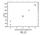
- Drain-source output resistances Rdsare provided in FIG. 22 as a function of estimated InGaN compositions for the In x Ga 1-x N (0 ⁇ x ⁇ 1) layer 38 of Sample 1 - 6 and Control 1 - 2 from the table of FIG. 20 . As shown, the structures of Control 1 - 2 without layer 38 may provide the lowest output resistances. When the In x Ga 1-x N (0 ⁇ x ⁇ 1) layer 38 is included (as in Sample 1 - 6 ), the output resistance may increase with increasing concentrations of indium in the In x Ga 1-x N (0 ⁇ x ⁇ 1) layer 38 .
- the high output resistance Rdsmay be an indication of reduced short-channel effects, and devices with higher output resistances may be expected to provide higher gain and/or Power Added Efficiency (PAE), especially when implemented in sub 0.2 ⁇ m (micrometer) gate length HEMTs for mm-wave applications.
- PAEPower Added Efficiency
- drain-source output resistances Rdsmay be increased in structures including energy barriers according to embodiments of the present invention as compared to structures of similar dimensions and materials without energy barriers.
- drain-source output resistances Rdsmay be increased by 10%, 50%, or even 100% as compared to structures of similar dimensions and materials but without an energy barrier.
- Confinementmay be improved with improved quality of the In x Ga 1-x N (0 ⁇ x ⁇ 1) layer 38 , and a relatively thin In x Ga 1-x N (0 ⁇ x ⁇ 1) layer 38 with a relatively high In (indium) mole fraction may provide a relatively high dipole and improved confinement.
- a high indium (In) content In x Ga 1-x N (0 ⁇ x ⁇ 1) layer 38may be difficult to grow with high crystal quality.
- An effective In x Ga 1-x N (0 ⁇ x ⁇ 1) layer 38may be provided with a relatively low In content (for example, having a mole fraction of InN in an InN/GaN alloy of about 5%) and a thickness in the range of about 10 ⁇ (Angstroms) to about 50 ⁇ (Angstroms).
- Heterojunction transistorssuch as HEMTs
- an epitaxial nucleation layer 13such as an AlN nucleation layer
- a single crystal substratesuch as a 4H—SiC substrate
- An epitaxial Group III nitride layer 36such as a layer of GaN may be formed on the nucleation layer 13
- an epitaxial Group III nitride energy barrier layer 38such as a layer of In x Ga 1-x N where 0 ⁇ x ⁇ 1 or where 0 ⁇ x ⁇ 1) may be formed on the layer 36 .
- An epitaxial Group III nitride low temperature protective layer 55(such as a layer of InAlGaN) may be formed on the energy barrier layer 38 , and an epitaxial Group III nitride channel layer 14 (such as a layer of InAlGaN) may be formed on the low temperature protective layer 55 .
- the low temperature protective layer 55may be formed at a temperature at least 100 degrees C. less than a temperature at which the channel layer 14 is formed.
- the low temperature protective layer 55may be formed at a temperature in the range of about 600 degrees C. to about 800 degrees C.
- the channel layer 14may be formed at a temperature of at least about 1000 degrees C.
- the low temperature protective layer 55may thus protect the energy barrier layer 38 during the subsequent step of forming the channel layer 14 , and the low temperature protective layer 55 may be considered a part of the channel layer 14 .
- an epitaxial Group III nitride barrier layer 16such as a layer of InAlGaN
- an epitaxial Group III nitride cap layer 17(such as a layer of InAlGaN) may be formed on the barrier layer 16 .
- source, gate, and drain contacts 18 , 22 , and 20 and passivation layer 52may be formed.
- Group III nitride compositions of the energy barrier layer 38 , the channel layer 14 , the barrier layer 16 , and the cap layer 17may vary.
- a concentration of gallium in the cap layer 17may be greater than a concentration of gallium in the barrier layer 16 .
- a concentration of aluminum in the barrier layer 16may exceed a concentration of aluminum in the channel layer 14 and/or the low temperature protective layer 55 .
- a concentration of indium in the energy barrier layer 38may exceed a concentration of indium in the channel layer 14 and/or the low temperature protective layer 55 .
- the energy barrier layer 38may comprise a layer of In x Ga 1-x N (0 ⁇ x ⁇ 1), the channel layer 14 may comprise a layer of Al y Ga 1-y N (0 ⁇ y ⁇ 1), and the barrier layer 16 may comprise a layer of Al z Ga 1-z N (0 ⁇ z ⁇ 1), and x, y, and/or z may be different. More particularly, the energy barrier layer 38 may comprise a layer of In x Ga 1-x N (0 ⁇ x ⁇ 1), the channel layer 14 may comprise a layer of GaN, the barrier layer 16 may comprise a layer of AlN, and the cap layer 17 may comprise a layer of Al n Ga 1-n N (0 ⁇ n ⁇ 1).
- HEMT structures according to embodiments of the present inventionmay provide improved power performance, for example, for mm-wave amplifiers for satellite communication, mm-wave WLAN (Wireless Local-Area Network), Digital Radio, solid-state amplifiers for vacuum tube replacement, and/or high frequency amplifiers for test and measurement applications.
- Power levels of 5 to 10 times that currently available using gallium-arsenide (GaAs) and/or indium-phosphorus (InP) transistorsmay be provided by HEMT structures according to embodiments of the present invention with relatively high efficiency and/or high power mm-wave amplifier operation.
- GaAsgallium-arsenide
- InPindium-phosphorus
- output characteristicsmay be improved by providing confinement from the backside of the GaN HEMT channel layer 14 .
- Performancemay be improved for HEMT structures operating at radio frequency (RF) and/or microwave frequencies, and even more significant improvements may be provided for HEMT structures operating at higher frequencies.
- RFradio frequency
- device output conductancemay be reduced linearly.
- on-resistancemay also decrease due to dimensional shrinkage, the reduction may be at a much lower rate so that power gain may be compromised, and improvement of extrinsic cut-off frequency f max with respect to f t may be less than desired.
- a sub-threshold leakagemay increase when the gate length is below 0.25 ⁇ m (micrometers) so that Power Added Efficiency (PAE) is reduced.
- PAEPower Added Efficiency
- an energy barriermay be provided using AlGaN based buffer layers.
- AlGaN layersmay tend to be unintentionally doped, and dopant compensation may cause deep traps.
- a crystal quality of bulk AlGaNmay generally be less than a crystal quality of currently available GaN, because the crystal formation process for AlGaN may be more complicated and may be subjected to alloy disorder.
- a layer of AlGaNmay be provided between the 2-DEG and a relatively high quality GaN buffer, but a buried sub-channel may form at the first AlGaN/GaN interface. Grading the AlGaN from the GaN buffer may reduce the sub-channel while generating bulk polarization charges, possibly reducing confinement.
- Exemplary embodiments described herein having heterostructures as a hole or electron sourceare illustrated with respect to Ga-polar epitaxial layers.
- such structureswould be the same for non-polar or partially Ga polar.
- non-polar structureswould not be able to take advantage of heterointerface polarization doping.
- Embodiments of the present invention employing N-polar structureswould look different in terms of the heterostructure layers, although the same principles apply, just reversed.
- the table of FIG. 23 aprovides drain-source resistances Rds in ohm mm, unity gain frequencies Ft, intr (i.e., frequencies at which current gain is 1, also referred to as Ft) in GHz, back-confinement values Vbc in ohm mm 2 GHz, device resistances Dr in ohm mm, and percentages of Indium in the InGaN layers 38 for the devices Sample 1 - 5 and Control 1 - 2 from the table of FIG. 20 .
- the graph of FIG. 23 billustrates back-confinement values Vbc as a function of percentage of Indium in the InGaN layer for the devices of FIG. 23 a.
- 23 cillustrates device resistances Dr as a function of percentage of Indium in the InGaN layer for the devices of FIG. 23 a. As shown in FIGS. 23 b and 23 c, both back-confinement values Vbc and device resistances Dr may improve with increasing Indium percentages.
- the gate contacts 22 of the devices represented in the tables of FIGS. 20 and 23 ainclude a field plate extending laterally on the passivation layer 52 0.15 ⁇ m (micrometer) towards the drain contact 20 and 0.2 ⁇ m (micrometers) toward the source contact 18 .
- the InGaN Layer 38has a thickness of 5 nm and varying mole fractions of InN in the InN/GaN alloy (defined by the indicated percentage) for each of Sample 1 - 5 , according to embodiments of the present invention. As discussed above, the percentage of Indium in the InGaN layers 38 is an estimate of a mole fraction of InN in an InN/GaN alloy of the InGaN layers 38 with the estimates being determined using photoluminescence (PL).
- PLphotoluminescence
- the InGaN Layer 38is omitted from the control structures Control 1 -Control 2 .
- Rdsis the drain-source output resistance measured in ohm mm
- Ft,intralso referred to as Ft
- Vbcis the back-confinement value measured in ohm mm 2 GHz
- Dris the device resistance measured in ohm mm.
- the gate length Lgis the distance from one side of the gate contact 22 adjacent the drain contact 18 to the other side of the gate contact 22 adjacent the source contact 20 shown in FIG. 19 in a direction parallel to the page of FIG. 19 .
- the gate width Wg(also referred to as the channel width) is the distance from one end of the gate contact 22 along the channel to a second end of the gate contact 22 along the channel in a direction perpendicular to the page of FIG. 19 .
- the separation between the gate contact 22 and the two dimensional electron gas (2DEG)is designated as d, and the separation d is approximately equal to the combined thicknesses of the cap layer 17 and the barrier layer 16 .
- the back-confinement value Vbc as calculated abovemay also represent a confinement potential per unit area of sheet-charge density (V/Ns*q) where V is the confinement potential, Ns is the sheet charge, and q is the unit electron charge.
- the gate length Lg for each of the deviceswas about 0.55 ⁇ m (micrometers), and the gate width Wg for each of the devices was about 246 ⁇ m (or 0.246 mm).
- Vbc (Sample3)(287.8 ohm mm)(27.7*10 ⁇ 6 mm
- a heterojunction transistormay include a channel layer 14 of a Group III nitride, a barrier layer 16 of a Group III nitride on the channel layer 14 wherein the barrier layer 16 has a bandgap greater than a bandgap of the channel layer 14 , a gate contact 22 on the barrier layer 16 so that the barrier layer 16 is between the gate contact 22 and the channel layer 14 , and source and drain contacts 18 and 20 on opposite sides of the gate contact 22 .
- an energy barrier 38 of InGaNmay be provided on the channel layer 14 so that the channel layer 14 is between the energy barrier 38 and the barrier layer 16 , and the energy barrier 38 may be configured to provide a back confinement value Vbc of at least about 0.21 ohm mm 2 GHz, and more particularly, a back confinement value Vbc of at least about 0.3 ohm mm 2 GHz. Moreover, the energy barrier 38 may be configured to provide back confinement values Vbc of at least approximately 0.21 ohm mm 2 GHz for unity gain frequencies Ft of at least about 35 GHz.
- the gate length Lg for each of the deviceswas about 0.55 ⁇ m (micrometers)
- the separation d for each of the deviceswas about 27 nm. Of the devices of FIGS.
- a heterojunction transistormay include a channel layer 14 of a Group III nitride, a barrier layer 16 of a Group III nitride on the channel layer 14 wherein the barrier layer 16 has a bandgap greater than a bandgap of the channel layer 14 .
- a gate contact 22may be provided on the barrier layer 16 so that the barrier layer 16 is between the gate contact 22 and the channel layer 14 , and source and drain contacts 18 and 20 may be provided on opposite sides of the gate contact 22 .
- an energy barrier 38 of InGaNmay be provided on the channel layer 14 so that the channel layer 14 is between the energy barrier 38 and the barrier layer 16 , and the energy barrier 38 may be configured to provide a device resistance Rd of at least about 9 ohm mm, and more particularly, a device resistance Rd of at least about 14 ohm mm.
- devices including InGaN back barrier layers according to embodiments of the present inventionmay provide higher on drain-source resistance Rds than devices without back barrier layers.
- Devices including InGaN back barrier layers according to embodiments of the present inventionmay provide a drain-source resistance Rds of at least about 170 ohm mm, and more particularly, a drain-source resistance Rds of at least about 240 ohm mm.
- the graphs of FIG. 24 aillustrate gain (G), power out (P OUT ), and power added efficiency (PAE) at 28 V Vds (drain-source voltage) and at 48 V Vds for a control device having a gate length Lg of 0.18 ⁇ m and a gate width Wg of 150 ⁇ m without an InGaN back barrier layer.
- the graphs of FIG. 24 billustrate gain (G), power out (P OUT ), and power added efficiency (PAE) at 28 V Vds (drain-source voltage) and at 48 V Vds for a device having a gate length Lg of 0.18 ⁇ m and a gate width Wg of 150 ⁇ m with an InGaN back barrier layer according to embodiments of the present invention.
- FIGS. 24 a and 24 bcircles are used to graph power added efficiency (PAE), diamonds are used to graph gain (G), and squares are used to graph power out (P OUT ). Moreover, open circles, diamonds, and squares are used for graphs at 28 V Vds; and closed circles, diamonds, and squares are used for graphs at 48 V Vds.
- the X-axis of the graphs of FIGS. 24 a and 24 brepresent power in (P IN )
- the graphs of FIG. 25 aillustrate drain currents (I D ) as a function of drain-source voltage (V DS ) at different gate-source voltages (Vgs) for the control device discussed above with respect to FIG. 24 a.
- a gate-source voltage of 4 Vwas provided for the uppermost graph, with a decrease of 1 V of Vgs being provided for each successive graph of FIG. 25 a.
- the graphs of FIG. 25 billustrate drain currents (I D ) as a function of drain-source voltage (V DS ) at different gate-source voltages (Vgs) for the device including an InGaN back barrier according to embodiments of the present invention as discussed above with respect to FIG. 24 b.
- a gate-source voltage of 4 Vwas provided for the uppermost graph, with a decrease of 1 V of Vgs being provided for each successive graph of FIG. 25 a.
- HEMT devices including InGaN back barrier layers according to embodiments of the present inventionmay provide about 14.1 W/mm and 65.6% PAE at 48 V Vds.
- the graphs of FIG. 26illustrate power added efficiency (PAE), power out (Pout), and gain (G) as functions of power in (Pin) for a HEMT structure having a 0.18 ⁇ m gate length (Lg) and a 150 ⁇ m gate width (Wg) according to embodiments of the present invention.
- the graphs of FIG. 27illustrate power added efficiency (PAE), power out (Pout), and gain (G) as functions of drain-source voltage (Vds) for a HEMT structure having a 0.18 ⁇ m gate length (Lg) and a 150 ⁇ m gate width (Wg) according to embodiments of the present invention.
- Vdsdrain-source voltage
- HEMT structuresmay provide at least 70% power added efficiency (PAE) and at least 10 W/mm power out (Pout) at a drain-source voltage (Vds) of about 38 V and at an operating frequency of about 10 GHz. More particularly, HEMT structures of FIGS. 26 and 27 may provide about 10.9 W/mm, about 70% power added efficiency, and about 14 dB of gain at a drain-source voltage (Vds) of about 38 V and at an operating frequency of about 10 GHz. Improved power added efficiency and power scaling may be provided according to embodiments of the present invention.
- PAEpower added efficiency
- Vdsdrain-source voltage
- Vdsdrain-source voltage
- Vdsdrain-source voltage
- Improved power added efficiency and power scalingmay be provided according to embodiments of the present invention.
- the graph of FIG. 28illustrates power out (Pout) as a function of time for HEMT structures according to embodiments of the present invention including a gate length Lg of 0.18 ⁇ m.
- HEMT structures according to embodimentsmay provide improved Room Temperature Operating Lifetime (RTOL) stability at a drain-source voltage (Vds) of 28 V. More particularly, less than 0.1 dB reduction of power out Pout may occur at room temperature operation at a drain-source voltage (Vds) of 28 V, at 5.5 W/mm power out, and at a 70% PAE operating point.
- RTOLRoom Temperature Operating Lifetime
- the graphs of FIG. 29illustrate power added efficiency (PAE), power out (Pout), and gain (G) as functions of power in (Pin) for a HEMT structure having a 0.18 ⁇ m gate length (Lg) and a 150 ⁇ m gate width (Wg) according to embodiments of the present invention.
- the HEMT structure of FIG. 29 including an InGaN back barrier layermay provide at least 50% PAE and 7 W/mm at 28 V drain-source voltage (Vds) and 35 GHz operating frequency. More particularly, the HEMT structure of FIG. 29 may provide about 52% PAE and about 7 W/mm at a 28 V drain-source voltage (Vds), 35 GHz operating frequency, and 7.5 dB Large Signal (LS) gain.
- the HEMT structure according to embodiments of the present invention used to provide the information of FIGS. 24 b, 25 b, 26 , 27 , 28 , and 29has the structure illustrated in FIG. 19 . More particularly, the HEMT structure of FIGS. 24 b, 25 b, 26 , 27 , 28 , and 29 includes an SiC substrate 12 , an InAlGaN buffer layer 13 , a GaN layer 36 , an InGaN energy/back barrier layer 38 having a thickness of about 5 nm (with a mole fraction of about 8% of InN in the InN/GaN alloy making up the InGaN layer 38 and doped with Silicon at a concentration of about 2E18 cm ⁇ 3 ), a GaN layer 14 having a thickness of about 10 nm, an AlN layer 16 having a thickness of about 0.8 nm, and an AlGaN layer 17 having a thickness of about 25 nm (with a mole fraction of 28% of AlN in the AlN/G
- the low temperature GaN layer 55is omitted.
- the gate 22may have a length Lg of about 0.18 ⁇ m and a width Wg of about 150 ⁇ m.
- the gate contact 22may include a field plate extending laterally on the passivation layer 52 0.15 ⁇ m (micrometer) towards the drain contact 20 and 0.2 ⁇ m (micrometers) toward the source contact 18 .
Landscapes
- Junction Field-Effect Transistors (AREA)
- Chemical & Material Sciences (AREA)
- Engineering & Computer Science (AREA)
- Materials Engineering (AREA)
Abstract
Description
Vbi=d*(q*Psheet)/∈
So, ifVbi<(Eg−Ea−Ed)/q
Thend×(q×Psheet)/∈<(Eg−Ea−Ed)/q
d×Psheet×(2×10⁻⁷V-cm)<(Eg−Ea−Ed)/q
d×Psheet<5×10⁶×(Eg−Ea−Ed)/q(V−1cm−1)
d×Psheet<2×5×106/cm=107/cm
d×Psheet<107/cm×104μm/cm
d×Psheet<1011μm/cm2
d<1011μm/cm2/Psheetor
d<0.1 μm
Vbc=Rds*Ft*d.
The back-confinement value Vbc as calculated above may also represent a confinement potential per unit area of sheet-charge density (V/Ns*q) where V is the confinement potential, Ns is the sheet charge, and q is the unit electron charge.
Vbc(Sample3)=(287.8 ohm mm)(27.7*10−6mm)(44 GHz)=0.35 ohm mm2GHz
Of the device of
Vbc(Sample4)=(197.8 ohm mm)(27.7*10−6mm)(39 GHz)=0.21 ohm mm2GHz
Of the devices (Control1 and Control2) of
Vbc(Control1)=(163.3 ohm mm)(27.7*10−6mm)(44 GHz)=0.20 ohm mm2GHz
Vbc(Control2)=(137.3 ohm mm)(27.7*10−6mm)(41 GHz)=0.16 ohm mm2GHz
Dr=Rds*d/Lg.
In the structures of
Dr(Sample3)=(287.8 ohm mm)(27.7 nm)/(550 nm)=14.5 ohm mm
Of the device of
Dr(Sample4)=(197.8 ohm mm)(27.7 nm)/(550 nm)=10 ohm mm
Of the devices (Control1 and Control2) of
Dr(Control1)=(163.3 ohm mm)(27.7 nm)/(550 nm)=8.2 ohm mm
Dr(Control2)=(137.3 ohm mm)(27.7 nm)/(550 nm)=6.9 ohm mm
Claims (44)
Priority Applications (5)
| Application Number | Priority Date | Filing Date | Title |
|---|---|---|---|
| US11/357,752US7612390B2 (en) | 2004-02-05 | 2006-02-17 | Heterojunction transistors including energy barriers |
| JP2006335974AJP5252800B2 (en) | 2006-02-17 | 2006-12-13 | Heterojunction transistors having energy barriers and related methods |
| EP06126233.3AEP1821344B1 (en) | 2006-02-17 | 2006-12-15 | Method of forming heterojunction tranistors including energy barriers |
| US12/566,973US9035354B2 (en) | 2004-02-05 | 2009-09-25 | Heterojunction transistors having barrier layer bandgaps greater than channel layer bandgaps and related methods |
| JP2012060000AJP2012164988A (en) | 2006-02-17 | 2012-03-16 | Heterojunction transistor having energy barrier and method related thereto |
Applications Claiming Priority (2)
| Application Number | Priority Date | Filing Date | Title |
|---|---|---|---|
| US10/772,882US7170111B2 (en) | 2004-02-05 | 2004-02-05 | Nitride heterojunction transistors having charge-transfer induced energy barriers and methods of fabricating the same |
| US11/357,752US7612390B2 (en) | 2004-02-05 | 2006-02-17 | Heterojunction transistors including energy barriers |
Related Parent Applications (1)
| Application Number | Title | Priority Date | Filing Date |
|---|---|---|---|
| US10/772,882Continuation-In-PartUS7170111B2 (en) | 2004-02-05 | 2004-02-05 | Nitride heterojunction transistors having charge-transfer induced energy barriers and methods of fabricating the same |
Related Child Applications (1)
| Application Number | Title | Priority Date | Filing Date |
|---|---|---|---|
| US12/566,973DivisionUS9035354B2 (en) | 2004-02-05 | 2009-09-25 | Heterojunction transistors having barrier layer bandgaps greater than channel layer bandgaps and related methods |
Publications (2)
| Publication Number | Publication Date |
|---|---|
| US20060255364A1 US20060255364A1 (en) | 2006-11-16 |
| US7612390B2true US7612390B2 (en) | 2009-11-03 |
Family
ID=38042492
Family Applications (2)
| Application Number | Title | Priority Date | Filing Date |
|---|---|---|---|
| US11/357,752Expired - LifetimeUS7612390B2 (en) | 2004-02-05 | 2006-02-17 | Heterojunction transistors including energy barriers |
| US12/566,973Expired - LifetimeUS9035354B2 (en) | 2004-02-05 | 2009-09-25 | Heterojunction transistors having barrier layer bandgaps greater than channel layer bandgaps and related methods |
Family Applications After (1)
| Application Number | Title | Priority Date | Filing Date |
|---|---|---|---|
| US12/566,973Expired - LifetimeUS9035354B2 (en) | 2004-02-05 | 2009-09-25 | Heterojunction transistors having barrier layer bandgaps greater than channel layer bandgaps and related methods |
Country Status (3)
| Country | Link |
|---|---|
| US (2) | US7612390B2 (en) |
| EP (1) | EP1821344B1 (en) |
| JP (2) | JP5252800B2 (en) |
Cited By (37)
| Publication number | Priority date | Publication date | Assignee | Title |
|---|---|---|---|---|
| US20090039392A1 (en)* | 2006-03-20 | 2009-02-12 | Thomas Herman | Iii-nitride power semiconductor device |
| US20100073067A1 (en)* | 2008-09-23 | 2010-03-25 | Transphorm Inc. | Inductive Load Power Switching Circuits |
| US8237198B2 (en) | 2008-12-10 | 2012-08-07 | Transphorm Inc. | Semiconductor heterostructure diodes |
| US8389977B2 (en) | 2009-12-10 | 2013-03-05 | Transphorm Inc. | Reverse side engineered III-nitride devices |
| US8390000B2 (en) | 2009-08-28 | 2013-03-05 | Transphorm Inc. | Semiconductor devices with field plates |
| CN103035699A (en)* | 2011-09-28 | 2013-04-10 | 富士通株式会社 | Compound semiconductor device and method of manufacturing the same |
| US20130175539A1 (en)* | 2012-01-11 | 2013-07-11 | Samsung Electronics Co., Ltd. | High electron mobility transistors and methods of manufacturing the same |
| US20130193441A1 (en)* | 2012-01-30 | 2013-08-01 | International Business Machines Corporation | Semiconductor Substrates Using Bandgap Material Between III-V Channel Material and Insulator Layer |
| US8519438B2 (en) | 2008-04-23 | 2013-08-27 | Transphorm Inc. | Enhancement mode III-N HEMTs |
| US8598937B2 (en) | 2011-10-07 | 2013-12-03 | Transphorm Inc. | High power semiconductor electronic components with increased reliability |
| US8643062B2 (en) | 2011-02-02 | 2014-02-04 | Transphorm Inc. | III-N device structures and methods |
| US8716141B2 (en) | 2011-03-04 | 2014-05-06 | Transphorm Inc. | Electrode configurations for semiconductor devices |
| US8742459B2 (en) | 2009-05-14 | 2014-06-03 | Transphorm Inc. | High voltage III-nitride semiconductor devices |
| US8742460B2 (en) | 2010-12-15 | 2014-06-03 | Transphorm Inc. | Transistors with isolation regions |
| US8772842B2 (en) | 2011-03-04 | 2014-07-08 | Transphorm, Inc. | Semiconductor diodes with low reverse bias currents |
| US8878246B2 (en) | 2010-06-14 | 2014-11-04 | Samsung Electronics Co., Ltd. | High electron mobility transistors and methods of fabricating the same |
| US8901604B2 (en) | 2011-09-06 | 2014-12-02 | Transphorm Inc. | Semiconductor devices with guard rings |
| US9035354B2 (en)* | 2004-02-05 | 2015-05-19 | Cree, Inc. | Heterojunction transistors having barrier layer bandgaps greater than channel layer bandgaps and related methods |
| US9041063B2 (en) | 2010-05-04 | 2015-05-26 | Samsung Electroncs Co., Ltd. | High electron mobility transistors and methods of manufacturing the same |
| US9093366B2 (en) | 2012-04-09 | 2015-07-28 | Transphorm Inc. | N-polar III-nitride transistors |
| US9165766B2 (en) | 2012-02-03 | 2015-10-20 | Transphorm Inc. | Buffer layer structures suited for III-nitride devices with foreign substrates |
| US9171730B2 (en) | 2013-02-15 | 2015-10-27 | Transphorm Inc. | Electrodes for semiconductor devices and methods of forming the same |
| US9184275B2 (en) | 2012-06-27 | 2015-11-10 | Transphorm Inc. | Semiconductor devices with integrated hole collectors |
| US9245992B2 (en) | 2013-03-15 | 2016-01-26 | Transphorm Inc. | Carbon doping semiconductor devices |
| US9257547B2 (en) | 2011-09-13 | 2016-02-09 | Transphorm Inc. | III-N device structures having a non-insulating substrate |
| US9318593B2 (en) | 2014-07-21 | 2016-04-19 | Transphorm Inc. | Forming enhancement mode III-nitride devices |
| US9412825B2 (en) | 2014-03-14 | 2016-08-09 | Kabushiki Kaisha Toshiba | Semiconductor device |
| US9443938B2 (en) | 2013-07-19 | 2016-09-13 | Transphorm Inc. | III-nitride transistor including a p-type depleting layer |
| US9536967B2 (en) | 2014-12-16 | 2017-01-03 | Transphorm Inc. | Recessed ohmic contacts in a III-N device |
| US9536966B2 (en) | 2014-12-16 | 2017-01-03 | Transphorm Inc. | Gate structures for III-N devices |
| US9590060B2 (en) | 2013-03-13 | 2017-03-07 | Transphorm Inc. | Enhancement-mode III-nitride devices |
| US20170098701A1 (en)* | 2015-10-02 | 2017-04-06 | Toyota Jidosha Kabushiki Kaisha | Semiconductor device |
| US10014375B1 (en) | 2017-07-26 | 2018-07-03 | Industrial Technology Research Institute | III-nitride based semiconductor structure |
| US10224401B2 (en) | 2016-05-31 | 2019-03-05 | Transphorm Inc. | III-nitride devices including a graded depleting layer |
| US10651307B2 (en) | 2018-07-23 | 2020-05-12 | Kabushiki Kaisha Toshiba | Semiconductor device and method for manufacturing the same |
| US11322599B2 (en) | 2016-01-15 | 2022-05-03 | Transphorm Technology, Inc. | Enhancement mode III-nitride devices having an Al1-xSixO gate insulator |
| US20220199816A1 (en)* | 2020-12-23 | 2022-06-23 | Intel Corporation | pGaN ENHANCEMENT MODE HEMTs WITH DOPANT DIFFUSION SPACER |
Families Citing this family (63)
| Publication number | Priority date | Publication date | Assignee | Title |
|---|---|---|---|---|
| JP2007088252A (en)* | 2005-09-22 | 2007-04-05 | Toyoda Gosei Co Ltd | Field effect transistor |
| US8193020B2 (en)* | 2006-11-15 | 2012-06-05 | The Regents Of The University Of California | Method for heteroepitaxial growth of high-quality N-face GaN, InN, and AlN and their alloys by metal organic chemical vapor deposition |
| CA2669228C (en)* | 2006-11-15 | 2014-12-16 | The Regents Of The University Of California | Method for heteroepitaxial growth of high-quality n-face gan, inn, and ain and their alloys by metal organic chemical vapor deposition |
| US7935985B2 (en)* | 2007-03-29 | 2011-05-03 | The Regents Of The University Of Califonia | N-face high electron mobility transistors with low buffer leakage and low parasitic resistance |
| US7713803B2 (en)* | 2007-03-29 | 2010-05-11 | Intel Corporation | Mechanism for forming a remote delta doping layer of a quantum well structure |
| KR100858821B1 (en)* | 2007-05-11 | 2008-09-17 | 삼성에스디아이 주식회사 | A thin film transistor, a method of manufacturing the same, and an organic light emitting display device including the thin film transistor and a method of manufacturing the same |
| JP2009027081A (en)* | 2007-07-23 | 2009-02-05 | Hitachi Cable Ltd | Semiconductor integrated circuit device and semiconductor switch device using the same |
| US7915643B2 (en) | 2007-09-17 | 2011-03-29 | Transphorm Inc. | Enhancement mode gallium nitride power devices |
| US7800132B2 (en) | 2007-10-25 | 2010-09-21 | Northrop Grumman Systems Corporation | High electron mobility transistor semiconductor device having field mitigating plate and fabrication method thereof |
| US20090140293A1 (en)* | 2007-11-29 | 2009-06-04 | General Electric Company | Heterostructure device and associated method |
| JP5032965B2 (en)* | 2007-12-10 | 2012-09-26 | パナソニック株式会社 | Nitride semiconductor transistor and manufacturing method thereof |
| KR101425131B1 (en)* | 2008-01-15 | 2014-07-31 | 삼성디스플레이 주식회사 | Display substrate and display device comprising the same |
| CN101981677B (en)* | 2008-03-24 | 2013-10-30 | 日本碍子株式会社 | Epitaxial substrate for semiconductor element, semiconductor element, and method for manufacturing epitaxial substrate for semiconductor element |
| EP2259287A4 (en) | 2008-03-24 | 2012-08-15 | Ngk Insulators Ltd | EPITACTICAL SUBSTRATE FOR A SEMICONDUCTOR COMPONENT, SEMICONDUCTOR COMPONENT AND METHOD FOR PRODUCING AN EPITACTICAL SUBSTRATE FOR A SEMICONDUCTOR COMPONENT |
| CN101604704B (en)* | 2008-06-13 | 2012-09-05 | 西安能讯微电子有限公司 | HEMT device and manufacturing method thereof |
| US8330170B2 (en) | 2008-12-05 | 2012-12-11 | Micron Technology, Inc. | Semiconductor device structures including transistors with energy barriers adjacent to transistor channels and associated methods |
| JP2010238752A (en)* | 2009-03-30 | 2010-10-21 | Mitsubishi Electric Corp | Semiconductor device and manufacturing method thereof |
| JP5413802B2 (en)* | 2009-06-19 | 2014-02-12 | トヨタ自動車株式会社 | Strain detector |
| JP2011009493A (en)* | 2009-06-26 | 2011-01-13 | Toshiba Corp | Semiconductor device, and method of manufacturing the same |
| US9306050B2 (en)* | 2009-06-26 | 2016-04-05 | Cornell University | III-V semiconductor structures including aluminum-silicon nitride passivation |
| JP5530682B2 (en)* | 2009-09-03 | 2014-06-25 | パナソニック株式会社 | Nitride semiconductor device |
| US8785305B2 (en)* | 2009-12-11 | 2014-07-22 | National Semiconductor Corporation | Backside stress compensation for gallium nitride or other nitride-based semiconductor devices |
| US8835998B2 (en)* | 2009-12-14 | 2014-09-16 | University Of Notre Dame Du Lac | Compositionally graded heterojunction semiconductor device and method of making same |
| JP5665171B2 (en)* | 2010-05-14 | 2015-02-04 | 住友電気工業株式会社 | Group III nitride semiconductor electronic device, method of fabricating group III nitride semiconductor electronic device |
| EP2587528B1 (en)* | 2010-06-24 | 2016-03-30 | The University Of Sheffield | Semiconductor device |
| KR101720589B1 (en)* | 2010-10-11 | 2017-03-30 | 삼성전자주식회사 | E-mode High Electron Mobility Transistor and method of manufacturing the same |
| JP5636867B2 (en) | 2010-10-19 | 2014-12-10 | 富士通株式会社 | Semiconductor device and manufacturing method of semiconductor device |
| JP5781292B2 (en)* | 2010-11-16 | 2015-09-16 | ローム株式会社 | Nitride semiconductor device and nitride semiconductor package |
| JP6017125B2 (en)* | 2011-09-16 | 2016-10-26 | ルネサスエレクトロニクス株式会社 | Semiconductor device and manufacturing method of semiconductor device |
| EP3540782A3 (en)* | 2011-10-11 | 2020-01-01 | Massachusetts Institute Of Technology | Semiconductor devices having a recessed electrode structure |
| US20130105817A1 (en) | 2011-10-26 | 2013-05-02 | Triquint Semiconductor, Inc. | High electron mobility transistor structure and method |
| US8912573B2 (en)* | 2013-02-26 | 2014-12-16 | Taiwan Semiconductor Manufacturing Company, Ltd. | Semiconductor device containing HEMT and MISFET and method of forming the same |
| US9406840B2 (en) | 2013-05-23 | 2016-08-02 | Sensor Electronic Technology, Inc. | Semiconductor layer including compositional inhomogeneities |
| US9281441B2 (en)* | 2013-05-23 | 2016-03-08 | Sensor Electronic Technology, Inc. | Semiconductor layer including compositional inhomogeneities |
| US9748440B2 (en) | 2013-05-23 | 2017-08-29 | Sensor Electronic Technology, Inc. | Semiconductor layer including compositional inhomogeneities |
| US10923623B2 (en) | 2013-05-23 | 2021-02-16 | Sensor Electronic Technology, Inc. | Semiconductor layer including compositional inhomogeneities |
| US20150021665A1 (en)* | 2013-07-17 | 2015-01-22 | Taiwan Semiconductor Manufacturing Company, Ltd. | Transistor having back-barrier layer and method of making the same |
| KR20150051822A (en)* | 2013-11-05 | 2015-05-13 | 삼성전자주식회사 | High electron mobility transistor and method of manufacturing the same |
| US9640650B2 (en)* | 2014-01-16 | 2017-05-02 | Qorvo Us, Inc. | Doped gallium nitride high-electron mobility transistor |
| US10867792B2 (en)* | 2014-02-18 | 2020-12-15 | Taiwan Semiconductor Manufacturing Company, Ltd. | High electron mobility transistor (HEMT) having an indium-containing layer and method of manufacturing the same |
| WO2015176002A1 (en)* | 2014-05-15 | 2015-11-19 | The Regents Of The University Of California | Doping in iii-nitride devices |
| US9620598B2 (en)* | 2014-08-05 | 2017-04-11 | Semiconductor Components Industries, Llc | Electronic device including a channel layer including gallium nitride |
| US10636881B2 (en)* | 2016-04-11 | 2020-04-28 | Qorvo Us, Inc. | High electron mobility transistor (HEMT) device |
| US10734512B2 (en) | 2016-04-11 | 2020-08-04 | Qorvo Us, Inc. | High electron mobility transistor (HEMT) device |
| CN107359242B (en)* | 2016-05-10 | 2019-08-23 | 上海新昇半导体科技有限公司 | Vacuum nano pipe field effect transistor and its manufacturing method |
| DE102017210711A1 (en)* | 2016-06-27 | 2017-12-28 | Fraunhofer-Gesellschaft zur Förderung der angewandten Forschung e.V. | Semiconductor device |
| US10411125B2 (en)* | 2016-11-23 | 2019-09-10 | Mitsubishi Electric Research Laboratories, Inc. | Semiconductor device having high linearity-transconductance |
| JP6966689B2 (en)* | 2017-03-31 | 2021-11-17 | 富士通株式会社 | Nitride semiconductor device and its manufacturing method |
| JP6993562B2 (en) | 2017-07-13 | 2022-02-03 | 富士通株式会社 | Compound semiconductor device and its manufacturing method |
| WO2019040083A1 (en)* | 2017-08-25 | 2019-02-28 | Hrl Laboratories, Llc | Digital alloy based back barrier for p-channel nitride transistors |
| US10651306B2 (en) | 2017-08-25 | 2020-05-12 | Hrl Laboratories, Llc | Digital alloy based back barrier for P-channel nitride transistors |
| US11094814B2 (en) | 2017-09-29 | 2021-08-17 | Epistar Corporation | Semiconductor power device |
| WO2019106843A1 (en)* | 2017-12-01 | 2019-06-06 | 三菱電機株式会社 | Method for producing semiconductor device and semiconductor device |
| US20190267481A1 (en)* | 2018-02-26 | 2019-08-29 | Duet Microelectronics LLC | Field-Effect Transistors (FETs) |
| US20190267480A1 (en)* | 2018-02-26 | 2019-08-29 | Duet Microelectronics Inc. | Anti-barrier-conduction (abc) spacers for high electron-mobility transistors (hemts) |
| JP6907974B2 (en)* | 2018-03-13 | 2021-07-21 | 株式会社デンソー | Semiconductor device |
| US11552075B2 (en)* | 2018-09-29 | 2023-01-10 | Intel Corporation | Group III-nitride (III-N) devices and methods of fabrication |
| US11522080B2 (en)* | 2018-11-07 | 2022-12-06 | Cornell University | High-voltage p-channel FET based on III-nitride heterostructures |
| US11239802B2 (en) | 2019-10-02 | 2022-02-01 | Wolfspeed, Inc. | Radio frequency transistor amplifiers having engineered instrinsic capacitances for improved performance |
| JP7543773B2 (en)* | 2020-08-25 | 2024-09-03 | 富士通株式会社 | Semiconductor device and its manufacturing method |
| US11942919B2 (en)* | 2021-01-11 | 2024-03-26 | Raytheon Company | Strain compensated rare earth group III-nitride heterostructures |
| JP2023033068A (en)* | 2021-08-25 | 2023-03-09 | 株式会社東芝 | Semiconductor device |
| US20240234560A9 (en)* | 2022-10-24 | 2024-07-11 | Northrop Grumman Systems Corporation | Back-barrier for gallium nitride based high electron mobility transistors |
Citations (109)
| Publication number | Priority date | Publication date | Assignee | Title |
|---|---|---|---|---|
| US2938136A (en) | 1958-08-26 | 1960-05-24 | Gen Electric | Electroluminescent lamp |
| US4424525A (en) | 1979-12-28 | 1984-01-03 | Fujitsu Limited | High electron mobility single heterojunction semiconductor devices |
| US4471366A (en) | 1979-03-28 | 1984-09-11 | Thomson-Csf | Field effect transistor with high cut-off frequency and process for forming same |
| US4727403A (en) | 1985-04-08 | 1988-02-23 | Nec Corporation | Double heterojunction semiconductor device with injector |
| US4755867A (en) | 1986-08-15 | 1988-07-05 | American Telephone And Telegraph Company, At&T Bell Laboratories | Vertical Enhancement-mode Group III-V compound MISFETs |
| US4788156A (en) | 1986-09-24 | 1988-11-29 | Microwave Technology, Inc. | Subchannel doping to reduce short-gate effects in field effect transistors |
| EP0334006A1 (en) | 1988-02-22 | 1989-09-27 | Siemens Aktiengesellschaft | Stacked channel heterojunction fet |
| US4946547A (en) | 1989-10-13 | 1990-08-07 | Cree Research, Inc. | Method of preparing silicon carbide surfaces for crystal growth |
| US5006914A (en) | 1988-12-02 | 1991-04-09 | Advanced Technology Materials, Inc. | Single crystal semiconductor substrate articles and semiconductor devices comprising same |
| US5030583A (en) | 1988-12-02 | 1991-07-09 | Advanced Technolgy Materials, Inc. | Method of making single crystal semiconductor substrate articles and semiconductor device |
| US5030586A (en) | 1985-11-13 | 1991-07-09 | Mitsubishi Denki Kabushiki Kaisha | Method for manufacturing semiconductor memory device having improved resistance to α particle induced soft errors |
| US5053348A (en) | 1989-12-01 | 1991-10-01 | Hughes Aircraft Company | Fabrication of self-aligned, t-gate hemt |
| US5172197A (en) | 1990-04-11 | 1992-12-15 | Hughes Aircraft Company | Hemt structure with passivated donor layer |
| US5192987A (en) | 1991-05-17 | 1993-03-09 | Apa Optics, Inc. | High electron mobility transistor with GaN/Alx Ga1-x N heterojunctions |
| US5200022A (en) | 1990-10-03 | 1993-04-06 | Cree Research, Inc. | Method of improving mechanically prepared substrate surfaces of alpha silicon carbide for deposition of beta silicon carbide thereon and resulting product |
| US5210051A (en) | 1990-03-27 | 1993-05-11 | Cree Research, Inc. | High efficiency light emitting diodes from bipolar gallium nitride |
| EP0563847A2 (en) | 1992-03-30 | 1993-10-06 | Matsushita Electric Industrial Co., Ltd. | A field effect transistor |
| WO1993023877A1 (en) | 1992-05-15 | 1993-11-25 | Massachusetts Institute Of Technology | Iii-v based integrated transistor |
| US5292501A (en) | 1990-06-25 | 1994-03-08 | Degenhardt Charles R | Use of a carboxy-substituted polymer to inhibit plaque formation without tooth staining |
| US5298445A (en) | 1992-05-22 | 1994-03-29 | Nec Corporation | Method for fabricating a field effect transistor |
| US5311055A (en) | 1991-11-22 | 1994-05-10 | The United States Of America As Represented By The Secretary Of The Navy | Trenched bipolar transistor structures |
| US5373171A (en) | 1987-03-12 | 1994-12-13 | Sumitomo Electric Industries, Ltd. | Thin film single crystal substrate |
| US5382822A (en) | 1992-09-25 | 1995-01-17 | Siemens Aktiengesellschaft | Metal-insulator semiconductor field-effect transistor |
| US5389571A (en) | 1991-12-18 | 1995-02-14 | Hiroshi Amano | Method of fabricating a gallium nitride based semiconductor device with an aluminum and nitrogen containing intermediate layer |
| USRE34861E (en) | 1987-10-26 | 1995-02-14 | North Carolina State University | Sublimation of silicon carbide to produce large, device quality single crystals of silicon carbide |
| US5393993A (en) | 1993-12-13 | 1995-02-28 | Cree Research, Inc. | Buffer structure between silicon carbide and gallium nitride and resulting semiconductor devices |
| US5422901A (en) | 1993-11-15 | 1995-06-06 | Motorola, Inc. | Semiconductor device with high heat conductivity |
| US5523589A (en) | 1994-09-20 | 1996-06-04 | Cree Research, Inc. | Vertical geometry light emitting diode with group III nitride active layer and extended lifetime |
| US5534462A (en) | 1995-02-24 | 1996-07-09 | Motorola, Inc. | Method for forming a plug and semiconductor device having the same |
| US5592501A (en) | 1994-09-20 | 1997-01-07 | Cree Research, Inc. | Low-strain laser structures with group III nitride active layers |
| US5661312A (en) | 1995-03-30 | 1997-08-26 | Motorola | Silicon carbide MOSFET |
| US5686737A (en) | 1994-09-16 | 1997-11-11 | Cree Research, Inc. | Self-aligned field-effect transistor for high frequency applications |
| US5700714A (en) | 1995-01-19 | 1997-12-23 | Oki Electric Industry Co., Ltd. | Diffusion mask and fabrication method for forming pn-junction elements in a compound semiconductor substrate |
| US5701019A (en) | 1993-03-12 | 1997-12-23 | Hitachi, Ltd. | Semiconductor device having first and second stacked semiconductor layers, with electrical contact to the first semiconductor layer |
| US5705827A (en) | 1991-12-25 | 1998-01-06 | Nec Corporation | Tunnel transistor and method of manufacturing same |
| JPH1050982A (en) | 1996-07-31 | 1998-02-20 | Nippon Telegr & Teleph Corp <Ntt> | Semiconductor device |
| US5804482A (en) | 1995-04-10 | 1998-09-08 | Abb Research Ltd. | Method for producing a semiconductor device having a semiconductor layer of SiC |
| US5872415A (en) | 1996-08-16 | 1999-02-16 | Kobe Steel Usa Inc. | Microelectronic structures including semiconductor islands |
| US5885860A (en) | 1995-06-30 | 1999-03-23 | Motorola, Inc. | Silicon carbide transistor and method |
| US5929467A (en)* | 1996-12-04 | 1999-07-27 | Sony Corporation | Field effect transistor with nitride compound |
| US5946547A (en) | 1995-12-22 | 1999-08-31 | Samsung Electronics Co., Ltd. | Liquid crystal display device fabrication methods with reduced numbers of patterning steps |
| JPH11261053A (en) | 1998-03-09 | 1999-09-24 | Furukawa Electric Co Ltd:The | High mobility transistor |
| US5990531A (en) | 1995-12-28 | 1999-11-23 | Philips Electronics N.A. Corporation | Methods of making high voltage GaN-AlN based semiconductor devices and semiconductor devices made |
| US6028328A (en) | 1996-01-03 | 2000-02-22 | Siemens Aktiengesellschaft | HEMT double hetero structure |
| US6046464A (en) | 1995-03-29 | 2000-04-04 | North Carolina State University | Integrated heterostructures of group III-V nitride semiconductor materials including epitaxial ohmic contact comprising multiple quantum well |
| US6064082A (en) | 1997-05-30 | 2000-05-16 | Sony Corporation | Heterojunction field effect transistor |
| US6086673A (en) | 1998-04-02 | 2000-07-11 | Massachusetts Institute Of Technology | Process for producing high-quality III-V nitride substrates |
| US6150239A (en) | 1997-05-31 | 2000-11-21 | Max Planck Society | Method for the transfer of thin layers monocrystalline material onto a desirable substrate |
| US6150680A (en) | 1998-03-05 | 2000-11-21 | Welch Allyn, Inc. | Field effect semiconductor device having dipole barrier |
| US6156581A (en) | 1994-01-27 | 2000-12-05 | Advanced Technology Materials, Inc. | GaN-based devices using (Ga, AL, In)N base layers |
| US6177685B1 (en) | 1998-01-20 | 2001-01-23 | Sharp Kabushiki Kaisha | Nitride-type III-V HEMT having an InN 2DEG channel layer |
| US6218680B1 (en) | 1999-05-18 | 2001-04-17 | Cree, Inc. | Semi-insulating silicon carbide without vanadium domination |
| WO2001057929A1 (en) | 2000-02-04 | 2001-08-09 | Cree Lighting Company | Group iii nitride based fets and hemts with reduced trapping and method for producing the same |
| US20010015446A1 (en) | 1999-12-08 | 2001-08-23 | Kaoru Inoue | Semiconductor device |
| JP2001230407A (en) | 1999-12-08 | 2001-08-24 | Matsushita Electric Ind Co Ltd | Semiconductor device |
| US20010020700A1 (en) | 2000-01-13 | 2001-09-13 | Kaoru Inoue | Semiconductor device |
| US6316826B1 (en) | 1998-10-02 | 2001-11-13 | Sumitomo Electric Industries, Ltd. | Semiconductor mounting package |
| US6316793B1 (en) | 1998-06-12 | 2001-11-13 | Cree, Inc. | Nitride based transistors on semi-insulating silicon carbide substrates |
| US20010040246A1 (en) | 2000-02-18 | 2001-11-15 | Hirotatsu Ishii | GaN field-effect transistor and method of manufacturing the same |
| JP2002016087A (en) | 2000-06-29 | 2002-01-18 | Nec Corp | Semiconductor device |
| US20020008241A1 (en) | 1997-10-07 | 2002-01-24 | Edmond John Adam | Group III nitride photonic devices on silicon carbide substrates with conductive buffer interlayer structure |
| US6396864B1 (en) | 1998-03-13 | 2002-05-28 | Jds Uniphase Corporation | Thermally conductive coatings for light emitting devices |
| US20020066908A1 (en) | 2000-12-01 | 2002-06-06 | Smith Richard Peter | Aluminum gallium nitride/gallium nitride high electron mobility transistors having a gate contact on a gallium nitride based cap segment and methods of fabricating same |
| JP3295267B2 (en) | 1995-03-24 | 2002-06-24 | 株式会社クボタ | Diesel engine subchamber combustion chamber |
| US20020079508A1 (en) | 2000-12-19 | 2002-06-27 | The Furukawa Electric Co., Ltd. | GaN-based high electron mobility transistor |
| US20020078881A1 (en) | 2000-11-30 | 2002-06-27 | Cuomo Jerome J. | Method and apparatus for producing M'''N columns and M'''N materials grown thereon |
| US20020086106A1 (en) | 2000-11-07 | 2002-07-04 | Park Chang-Soo | Apparatus and method for thin film deposition |
| US20020096104A1 (en) | 2001-01-19 | 2002-07-25 | Hoya Corporation | Single crystal SiCand method of producing the same as well as SiC semiconductor device and SiC composite material |
| US6429467B1 (en) | 1999-01-29 | 2002-08-06 | Nec Corporation | Heterojunction field effect transistor |
| US20020119610A1 (en) | 2001-02-27 | 2002-08-29 | Katsunori Nishii | Semiconductor device and method for fabricating the same |
| US20020117695A1 (en) | 2001-02-23 | 2002-08-29 | Ricardo Borges | Gallium nitride materials including thermally conductive regions |
| US20020123204A1 (en) | 2001-03-01 | 2002-09-05 | Torvik John Tarje | Method of making a hybrid substrate having a thin silicon carbide membrane layer |
| US6448648B1 (en) | 1997-03-27 | 2002-09-10 | The United States Of America As Represented By The Secretary Of The Navy | Metalization of electronic semiconductor devices |
| JP2002265296A (en) | 2001-03-09 | 2002-09-18 | Kobe Steel Ltd | Diamond thin film and manufacturing method therefor |
| US20020167023A1 (en) | 2001-05-11 | 2002-11-14 | Cree Lighting Company And Regents Of The University Of California | Group-III nitride based high electron mobility transistor (HEMT) with barrier/spacer layer |
| US20020182779A1 (en) | 2000-01-27 | 2002-12-05 | Bewley William W. | Heat sink method and system |
| US20020180351A1 (en) | 2001-04-30 | 2002-12-05 | Mcnulty Thomas Francis | UV reflectors and UV-based light sources having reduced UV radiation leakage incorporating the same |
| US6497763B2 (en) | 2001-01-19 | 2002-12-24 | The United States Of America As Represented By The Secretary Of The Navy | Electronic device with composite substrate |
| US20030017683A1 (en) | 2001-07-18 | 2003-01-23 | Motorola, Inc. | Structure and method for fabricating heterojunction bipolar transistors and high electron mobility transistors utilizing the formation of a complaint substrates for materials used to form the same |
| US20030020092A1 (en) | 2001-07-24 | 2003-01-30 | Primit Parikh | Insulating gate AlGaN/GaN HEMT |
| US6515316B1 (en) | 2000-07-14 | 2003-02-04 | Trw Inc. | Partially relaxed channel HEMT device |
| US20030025198A1 (en) | 2001-07-31 | 2003-02-06 | Chrysler Gregory M. | Electronic assembly including a die having an integrated circuit and a layer of diamond to transfer heat |
| JP2003037074A (en) | 2001-07-26 | 2003-02-07 | Toshiba Corp | Semiconductor device and method of manufacturing the same |
| US6533874B1 (en) | 1996-12-03 | 2003-03-18 | Advanced Technology Materials, Inc. | GaN-based devices using thick (Ga, Al, In)N base layers |
| US20030096507A1 (en) | 2001-11-20 | 2003-05-22 | Baker Faye D. | Backside protection films |
| US20030102482A1 (en) | 2001-12-03 | 2003-06-05 | Saxler Adam William | Strain balanced nitride heterojunction transistors and methods of fabricating strain balanced nitride heterojunction transistors |
| US20030107045A1 (en) | 2000-07-06 | 2003-06-12 | Dominik Eisert | Radiation-emitting semiconductor chip, and method for producing the semiconductor chip |
| US20030123829A1 (en) | 1996-10-16 | 2003-07-03 | Taylor Geoff W. | Monolithic integrated circuit including a waveguide and quantum well inversion channel devices and a method of fabricating same |
| US20030127654A1 (en) | 2000-02-15 | 2003-07-10 | Dominik Eisert | Semiconductor component which emits radiation, and method for producing the same |
| US20030145784A1 (en) | 1999-04-08 | 2003-08-07 | Thompson Margarita P. | Cubic (zinc-blende) aluminum nitride and method of making same |
| JP2003257804A (en) | 2002-02-27 | 2003-09-12 | Sony Corp | Composite substrate and substrate manufacturing method |
| WO2003036699A3 (en) | 2001-10-23 | 2003-09-25 | Cambridge Semiconductor Ltd | Lateral semiconductor-on-insulator structure and corresponding manufacturing methods |
| US6634770B2 (en) | 2001-08-24 | 2003-10-21 | Densen Cao | Light source using semiconductor devices mounted on a heat sink |
| US20030213975A1 (en) | 2002-05-17 | 2003-11-20 | Matsushita Electric Industrial Co, Ltd. | Semiconductor device |
| US20030219959A1 (en) | 2000-11-27 | 2003-11-27 | Bruno Ghyselen | Methods for fabricating final substrates |
| US6670693B1 (en) | 1996-12-05 | 2003-12-30 | Nathaniel R. Quick | Laser synthesized wide-bandgap semiconductor electronic devices and circuits |
| US20040004223A1 (en) | 1997-01-09 | 2004-01-08 | Nichia Chemical Industries, Ltd. | Nitride semiconductor device |
| US20040009649A1 (en) | 2002-07-12 | 2004-01-15 | Kub Francis J. | Wafer bonding of thinned electronic materials and circuits to high performance substrates |
| WO2004008495A2 (en) | 2002-07-16 | 2004-01-22 | Cree, Inc. | Nitride-based transistors and methods of fabrication thereof using non-etched contact recesses |
| US20040023468A1 (en) | 2002-01-22 | 2004-02-05 | Bruno Ghyselen | Method for manufacturing a free-standing substrate made of monocrystalline semi-conductor material |
| US20040021152A1 (en) | 2002-08-05 | 2004-02-05 | Chanh Nguyen | Ga/A1GaN Heterostructure Field Effect Transistor with dielectric recessed gate |
| US20040029330A1 (en) | 2002-08-05 | 2004-02-12 | Tahir Hussain | Ohmic metal contact and channel protection in GaN devices using an encapsulation layer |
| US20040051141A1 (en) | 2002-06-26 | 2004-03-18 | Cambridge Semiconductor Limited | Lateral semiconductor device |
| US20040066908A1 (en) | 2000-10-11 | 2004-04-08 | Randolf Hanke | Method and device for the representing an object by means of an irradiation and for reconstructing said object |
| US6757314B2 (en) | 1998-12-30 | 2004-06-29 | Xerox Corporation | Structure for nitride based laser diode with growth substrate removed |
| JP2004342810A (en) | 2003-05-15 | 2004-12-02 | Fujitsu Ltd | Compound semiconductor device |
| US20040241970A1 (en) | 2000-04-11 | 2004-12-02 | Zoltan Ring | Method of Forming Vias in Silicon Carbide and Resulting Devices and Circuits |
| US20050164482A1 (en) | 2004-01-22 | 2005-07-28 | Cree, Inc. | Silicon Carbide on Diamond Substrates and Related Devices and Methods |
| US7042153B2 (en)* | 2002-02-12 | 2006-05-09 | Toyoda Gosei Co., Ltd. | Group III nitride compound semiconductor light emitting element |
Family Cites Families (42)
| Publication number | Priority date | Publication date | Assignee | Title |
|---|---|---|---|---|
| JPS5353983U (en) | 1976-10-12 | 1978-05-09 | ||
| JPS5936837B2 (en) | 1977-04-05 | 1984-09-06 | 株式会社東芝 | Optical semiconductor device |
| JPH0434084Y2 (en)* | 1985-12-20 | 1992-08-14 | ||
| JPH0770706B2 (en) | 1986-06-30 | 1995-07-31 | 富士通株式会社 | High-speed semiconductor device |
| JPH03227533A (en) | 1990-02-01 | 1991-10-08 | Nec Corp | Semiconductor device |
| JPH0722614A (en) | 1993-07-06 | 1995-01-24 | Hitachi Cable Ltd | Compound semiconductor epitaxial wafer |
| US5778156A (en)* | 1996-05-08 | 1998-07-07 | Xerox Corporation | Method and system for implementing fuzzy image processing of image data |
| JPH11111730A (en) | 1997-09-30 | 1999-04-23 | Sanyo Electric Co Ltd | Semiconductor device |
| US6023328A (en)* | 1998-02-23 | 2000-02-08 | Micron Technology, Inc. | Photomask inspection method and apparatus |
| JPH11251638A (en) | 1998-03-03 | 1999-09-17 | Yamaha Corp | Brightness adjustable device |
| JP2000068498A (en) | 1998-08-21 | 2000-03-03 | Nippon Telegr & Teleph Corp <Ntt> | Insulating nitride film and semiconductor device using the same |
| JP3129298B2 (en) | 1998-11-11 | 2001-01-29 | 日本電気株式会社 | Field effect transistor and method of manufacturing the same |
| JP2001127281A (en) | 1999-10-26 | 2001-05-11 | Murata Mfg Co Ltd | Semiconductor device |
| JP4278820B2 (en)* | 2000-03-31 | 2009-06-17 | パイオニア株式会社 | optical disk |
| JP2001283470A (en)* | 2000-03-31 | 2001-10-12 | Pioneer Electronic Corp | System and method for recording information |
| US6624452B2 (en) | 2000-07-28 | 2003-09-23 | The Regents Of The University Of California | Gallium nitride-based HFET and a method for fabricating a gallium nitride-based HFET |
| US6998281B2 (en) | 2000-10-12 | 2006-02-14 | General Electric Company | Solid state lighting device with reduced form factor including LED with directional emission and package with microoptics |
| JP3738824B2 (en) | 2000-12-26 | 2006-01-25 | セイコーエプソン株式会社 | OPTICAL DEVICE, ITS MANUFACTURING METHOD, AND ELECTRONIC DEVICE |
| JP3987360B2 (en) | 2002-03-22 | 2007-10-10 | 日本碍子株式会社 | Epitaxial substrate, epitaxial substrate for electronic device, and electronic device |
| US6983475B2 (en)* | 2002-03-26 | 2006-01-03 | Hewlett-Packard Development Company, L.P. | Method and data storage device that utilizes blocking material |
| JP4385205B2 (en) | 2002-12-16 | 2009-12-16 | 日本電気株式会社 | Field effect transistor |
| US7812369B2 (en) | 2003-09-09 | 2010-10-12 | The Regents Of The University Of California | Fabrication of single or multiple gate field plates |
| US7135715B2 (en) | 2004-01-07 | 2006-11-14 | Cree, Inc. | Co-doping for fermi level control in semi-insulating Group III nitrides |
| US7045404B2 (en) | 2004-01-16 | 2006-05-16 | Cree, Inc. | Nitride-based transistors with a protective layer and a low-damage recess and methods of fabrication thereof |
| JP4449467B2 (en) | 2004-01-28 | 2010-04-14 | サンケン電気株式会社 | Semiconductor device |
| US7612390B2 (en)* | 2004-02-05 | 2009-11-03 | Cree, Inc. | Heterojunction transistors including energy barriers |
| US7170111B2 (en)* | 2004-02-05 | 2007-01-30 | Cree, Inc. | Nitride heterojunction transistors having charge-transfer induced energy barriers and methods of fabricating the same |
| US7432142B2 (en) | 2004-05-20 | 2008-10-07 | Cree, Inc. | Methods of fabricating nitride-based transistors having regrown ohmic contact regions |
| US7084441B2 (en) | 2004-05-20 | 2006-08-01 | Cree, Inc. | Semiconductor devices having a hybrid channel layer, current aperture transistors and methods of fabricating same |
| US7332795B2 (en) | 2004-05-22 | 2008-02-19 | Cree, Inc. | Dielectric passivation for semiconductor devices |
| JP4468744B2 (en) | 2004-06-15 | 2010-05-26 | 日本電信電話株式会社 | Method for producing nitride semiconductor thin film |
| US7238560B2 (en) | 2004-07-23 | 2007-07-03 | Cree, Inc. | Methods of fabricating nitride-based transistors with a cap layer and a recessed gate |
| US20060017064A1 (en) | 2004-07-26 | 2006-01-26 | Saxler Adam W | Nitride-based transistors having laterally grown active region and methods of fabricating same |
| US7456443B2 (en) | 2004-11-23 | 2008-11-25 | Cree, Inc. | Transistors having buried n-type and p-type regions beneath the source region |
| US7161194B2 (en) | 2004-12-06 | 2007-01-09 | Cree, Inc. | High power density and/or linearity transistors |
| US7355215B2 (en) | 2004-12-06 | 2008-04-08 | Cree, Inc. | Field effect transistors (FETs) having multi-watt output power at millimeter-wave frequencies |
| US7465967B2 (en) | 2005-03-15 | 2008-12-16 | Cree, Inc. | Group III nitride field effect transistors (FETS) capable of withstanding high temperature reverse bias test conditions |
| US8575651B2 (en) | 2005-04-11 | 2013-11-05 | Cree, Inc. | Devices having thick semi-insulating epitaxial gallium nitride layer |
| US7626217B2 (en) | 2005-04-11 | 2009-12-01 | Cree, Inc. | Composite substrates of conductive and insulating or semi-insulating group III-nitrides for group III-nitride devices |
| US7615774B2 (en) | 2005-04-29 | 2009-11-10 | Cree.Inc. | Aluminum free group III-nitride based high electron mobility transistors |
| US7544963B2 (en) | 2005-04-29 | 2009-06-09 | Cree, Inc. | Binary group III-nitride based high electron mobility transistors |
| US7446626B2 (en)* | 2006-09-08 | 2008-11-04 | Stmicroelectronics Ltd. | Directional couplers for RF power detection |
- 2006
- 2006-02-17USUS11/357,752patent/US7612390B2/ennot_activeExpired - Lifetime
- 2006-12-13JPJP2006335974Apatent/JP5252800B2/enactiveActive
- 2006-12-15EPEP06126233.3Apatent/EP1821344B1/enactiveActive
- 2009
- 2009-09-25USUS12/566,973patent/US9035354B2/ennot_activeExpired - Lifetime
- 2012
- 2012-03-16JPJP2012060000Apatent/JP2012164988A/enactivePending
Patent Citations (124)
| Publication number | Priority date | Publication date | Assignee | Title |
|---|---|---|---|---|
| US2938136A (en) | 1958-08-26 | 1960-05-24 | Gen Electric | Electroluminescent lamp |
| US4471366A (en) | 1979-03-28 | 1984-09-11 | Thomson-Csf | Field effect transistor with high cut-off frequency and process for forming same |
| US4424525A (en) | 1979-12-28 | 1984-01-03 | Fujitsu Limited | High electron mobility single heterojunction semiconductor devices |
| US4727403A (en) | 1985-04-08 | 1988-02-23 | Nec Corporation | Double heterojunction semiconductor device with injector |
| US5030586A (en) | 1985-11-13 | 1991-07-09 | Mitsubishi Denki Kabushiki Kaisha | Method for manufacturing semiconductor memory device having improved resistance to α particle induced soft errors |
| US4755867A (en) | 1986-08-15 | 1988-07-05 | American Telephone And Telegraph Company, At&T Bell Laboratories | Vertical Enhancement-mode Group III-V compound MISFETs |
| US4788156A (en) | 1986-09-24 | 1988-11-29 | Microwave Technology, Inc. | Subchannel doping to reduce short-gate effects in field effect transistors |
| US5373171A (en) | 1987-03-12 | 1994-12-13 | Sumitomo Electric Industries, Ltd. | Thin film single crystal substrate |
| USRE34861E (en) | 1987-10-26 | 1995-02-14 | North Carolina State University | Sublimation of silicon carbide to produce large, device quality single crystals of silicon carbide |
| EP0334006A1 (en) | 1988-02-22 | 1989-09-27 | Siemens Aktiengesellschaft | Stacked channel heterojunction fet |
| US5030583A (en) | 1988-12-02 | 1991-07-09 | Advanced Technolgy Materials, Inc. | Method of making single crystal semiconductor substrate articles and semiconductor device |
| US5006914A (en) | 1988-12-02 | 1991-04-09 | Advanced Technology Materials, Inc. | Single crystal semiconductor substrate articles and semiconductor devices comprising same |
| US4946547A (en) | 1989-10-13 | 1990-08-07 | Cree Research, Inc. | Method of preparing silicon carbide surfaces for crystal growth |
| US5053348A (en) | 1989-12-01 | 1991-10-01 | Hughes Aircraft Company | Fabrication of self-aligned, t-gate hemt |
| US5210051A (en) | 1990-03-27 | 1993-05-11 | Cree Research, Inc. | High efficiency light emitting diodes from bipolar gallium nitride |
| US5172197A (en) | 1990-04-11 | 1992-12-15 | Hughes Aircraft Company | Hemt structure with passivated donor layer |
| US5292501A (en) | 1990-06-25 | 1994-03-08 | Degenhardt Charles R | Use of a carboxy-substituted polymer to inhibit plaque formation without tooth staining |
| US5200022A (en) | 1990-10-03 | 1993-04-06 | Cree Research, Inc. | Method of improving mechanically prepared substrate surfaces of alpha silicon carbide for deposition of beta silicon carbide thereon and resulting product |
| US5296395A (en) | 1991-05-17 | 1994-03-22 | Apa Optics, Inc. | Method of making a high electron mobility transistor |
| US5192987A (en) | 1991-05-17 | 1993-03-09 | Apa Optics, Inc. | High electron mobility transistor with GaN/Alx Ga1-x N heterojunctions |
| US5311055A (en) | 1991-11-22 | 1994-05-10 | The United States Of America As Represented By The Secretary Of The Navy | Trenched bipolar transistor structures |
| US5389571A (en) | 1991-12-18 | 1995-02-14 | Hiroshi Amano | Method of fabricating a gallium nitride based semiconductor device with an aluminum and nitrogen containing intermediate layer |
| US5705827A (en) | 1991-12-25 | 1998-01-06 | Nec Corporation | Tunnel transistor and method of manufacturing same |
| EP0563847A2 (en) | 1992-03-30 | 1993-10-06 | Matsushita Electric Industrial Co., Ltd. | A field effect transistor |
| WO1993023877A1 (en) | 1992-05-15 | 1993-11-25 | Massachusetts Institute Of Technology | Iii-v based integrated transistor |
| US5298445A (en) | 1992-05-22 | 1994-03-29 | Nec Corporation | Method for fabricating a field effect transistor |
| US5382822A (en) | 1992-09-25 | 1995-01-17 | Siemens Aktiengesellschaft | Metal-insulator semiconductor field-effect transistor |
| US5701019A (en) | 1993-03-12 | 1997-12-23 | Hitachi, Ltd. | Semiconductor device having first and second stacked semiconductor layers, with electrical contact to the first semiconductor layer |
| US5422901A (en) | 1993-11-15 | 1995-06-06 | Motorola, Inc. | Semiconductor device with high heat conductivity |
| US5393993A (en) | 1993-12-13 | 1995-02-28 | Cree Research, Inc. | Buffer structure between silicon carbide and gallium nitride and resulting semiconductor devices |
| US6156581A (en) | 1994-01-27 | 2000-12-05 | Advanced Technology Materials, Inc. | GaN-based devices using (Ga, AL, In)N base layers |
| US5686737A (en) | 1994-09-16 | 1997-11-11 | Cree Research, Inc. | Self-aligned field-effect transistor for high frequency applications |
| US5592501A (en) | 1994-09-20 | 1997-01-07 | Cree Research, Inc. | Low-strain laser structures with group III nitride active layers |
| US5523589A (en) | 1994-09-20 | 1996-06-04 | Cree Research, Inc. | Vertical geometry light emitting diode with group III nitride active layer and extended lifetime |
| US5700714A (en) | 1995-01-19 | 1997-12-23 | Oki Electric Industry Co., Ltd. | Diffusion mask and fabrication method for forming pn-junction elements in a compound semiconductor substrate |
| US5534462A (en) | 1995-02-24 | 1996-07-09 | Motorola, Inc. | Method for forming a plug and semiconductor device having the same |
| JP3295267B2 (en) | 1995-03-24 | 2002-06-24 | 株式会社クボタ | Diesel engine subchamber combustion chamber |
| US6046464A (en) | 1995-03-29 | 2000-04-04 | North Carolina State University | Integrated heterostructures of group III-V nitride semiconductor materials including epitaxial ohmic contact comprising multiple quantum well |
| US5661312A (en) | 1995-03-30 | 1997-08-26 | Motorola | Silicon carbide MOSFET |
| US5804482A (en) | 1995-04-10 | 1998-09-08 | Abb Research Ltd. | Method for producing a semiconductor device having a semiconductor layer of SiC |
| US5885860A (en) | 1995-06-30 | 1999-03-23 | Motorola, Inc. | Silicon carbide transistor and method |
| US5946547A (en) | 1995-12-22 | 1999-08-31 | Samsung Electronics Co., Ltd. | Liquid crystal display device fabrication methods with reduced numbers of patterning steps |
| US5990531A (en) | 1995-12-28 | 1999-11-23 | Philips Electronics N.A. Corporation | Methods of making high voltage GaN-AlN based semiconductor devices and semiconductor devices made |
| US6028328A (en) | 1996-01-03 | 2000-02-22 | Siemens Aktiengesellschaft | HEMT double hetero structure |
| JPH1050982A (en) | 1996-07-31 | 1998-02-20 | Nippon Telegr & Teleph Corp <Ntt> | Semiconductor device |
| US5872415A (en) | 1996-08-16 | 1999-02-16 | Kobe Steel Usa Inc. | Microelectronic structures including semiconductor islands |
| US20030123829A1 (en) | 1996-10-16 | 2003-07-03 | Taylor Geoff W. | Monolithic integrated circuit including a waveguide and quantum well inversion channel devices and a method of fabricating same |
| US6533874B1 (en) | 1996-12-03 | 2003-03-18 | Advanced Technology Materials, Inc. | GaN-based devices using thick (Ga, Al, In)N base layers |
| US5929467A (en)* | 1996-12-04 | 1999-07-27 | Sony Corporation | Field effect transistor with nitride compound |
| US6670693B1 (en) | 1996-12-05 | 2003-12-30 | Nathaniel R. Quick | Laser synthesized wide-bandgap semiconductor electronic devices and circuits |
| US20040004223A1 (en) | 1997-01-09 | 2004-01-08 | Nichia Chemical Industries, Ltd. | Nitride semiconductor device |
| US6448648B1 (en) | 1997-03-27 | 2002-09-10 | The United States Of America As Represented By The Secretary Of The Navy | Metalization of electronic semiconductor devices |
| US6064082A (en) | 1997-05-30 | 2000-05-16 | Sony Corporation | Heterojunction field effect transistor |
| US6150239A (en) | 1997-05-31 | 2000-11-21 | Max Planck Society | Method for the transfer of thin layers monocrystalline material onto a desirable substrate |
| US20020008241A1 (en) | 1997-10-07 | 2002-01-24 | Edmond John Adam | Group III nitride photonic devices on silicon carbide substrates with conductive buffer interlayer structure |
| US6177685B1 (en) | 1998-01-20 | 2001-01-23 | Sharp Kabushiki Kaisha | Nitride-type III-V HEMT having an InN 2DEG channel layer |
| US6150680A (en) | 1998-03-05 | 2000-11-21 | Welch Allyn, Inc. | Field effect semiconductor device having dipole barrier |
| JPH11261053A (en) | 1998-03-09 | 1999-09-24 | Furukawa Electric Co Ltd:The | High mobility transistor |
| US6396864B1 (en) | 1998-03-13 | 2002-05-28 | Jds Uniphase Corporation | Thermally conductive coatings for light emitting devices |
| US6086673A (en) | 1998-04-02 | 2000-07-11 | Massachusetts Institute Of Technology | Process for producing high-quality III-V nitride substrates |
| US6316793B1 (en) | 1998-06-12 | 2001-11-13 | Cree, Inc. | Nitride based transistors on semi-insulating silicon carbide substrates |
| US6583454B2 (en) | 1998-06-12 | 2003-06-24 | Cree, Inc. | Nitride based transistors on semi-insulating silicon carbide substrates |
| US6316826B1 (en) | 1998-10-02 | 2001-11-13 | Sumitomo Electric Industries, Ltd. | Semiconductor mounting package |
| US6757314B2 (en) | 1998-12-30 | 2004-06-29 | Xerox Corporation | Structure for nitride based laser diode with growth substrate removed |
| US6429467B1 (en) | 1999-01-29 | 2002-08-06 | Nec Corporation | Heterojunction field effect transistor |
| US20030145784A1 (en) | 1999-04-08 | 2003-08-07 | Thompson Margarita P. | Cubic (zinc-blende) aluminum nitride and method of making same |
| US6218680B1 (en) | 1999-05-18 | 2001-04-17 | Cree, Inc. | Semi-insulating silicon carbide without vanadium domination |
| US6639255B2 (en) | 1999-12-08 | 2003-10-28 | Matsushita Electric Industrial Co., Ltd. | GaN-based HFET having a surface-leakage reducing cap layer |
| US20010015446A1 (en) | 1999-12-08 | 2001-08-23 | Kaoru Inoue | Semiconductor device |
| JP2001230407A (en) | 1999-12-08 | 2001-08-24 | Matsushita Electric Ind Co Ltd | Semiconductor device |
| US20010020700A1 (en) | 2000-01-13 | 2001-09-13 | Kaoru Inoue | Semiconductor device |
| US20020182779A1 (en) | 2000-01-27 | 2002-12-05 | Bewley William W. | Heat sink method and system |
| WO2001057929A1 (en) | 2000-02-04 | 2001-08-09 | Cree Lighting Company | Group iii nitride based fets and hemts with reduced trapping and method for producing the same |
| US6586781B2 (en) | 2000-02-04 | 2003-07-01 | Cree Lighting Company | Group III nitride based FETs and HEMTs with reduced trapping and method for producing the same |
| US20010023964A1 (en) | 2000-02-04 | 2001-09-27 | Yifeng Wu | Group III nitride based FETs and hemts with reduced trapping and method for producing the same |
| US20030127654A1 (en) | 2000-02-15 | 2003-07-10 | Dominik Eisert | Semiconductor component which emits radiation, and method for producing the same |
| US20010040246A1 (en) | 2000-02-18 | 2001-11-15 | Hirotatsu Ishii | GaN field-effect transistor and method of manufacturing the same |
| US20040241970A1 (en) | 2000-04-11 | 2004-12-02 | Zoltan Ring | Method of Forming Vias in Silicon Carbide and Resulting Devices and Circuits |
| JP2002016087A (en) | 2000-06-29 | 2002-01-18 | Nec Corp | Semiconductor device |
| US6492669B2 (en) | 2000-06-29 | 2002-12-10 | Nec Corporation | Semiconductor device with schottky electrode having high schottky barrier |
| US20020017696A1 (en) | 2000-06-29 | 2002-02-14 | Tatsuo Nakayama | Semiconductor device with schottky electrode having high schottky barrier |
| US20030107045A1 (en) | 2000-07-06 | 2003-06-12 | Dominik Eisert | Radiation-emitting semiconductor chip, and method for producing the semiconductor chip |
| US6515316B1 (en) | 2000-07-14 | 2003-02-04 | Trw Inc. | Partially relaxed channel HEMT device |
| US20040066908A1 (en) | 2000-10-11 | 2004-04-08 | Randolf Hanke | Method and device for the representing an object by means of an irradiation and for reconstructing said object |
| US20020086106A1 (en) | 2000-11-07 | 2002-07-04 | Park Chang-Soo | Apparatus and method for thin film deposition |
| US6867067B2 (en) | 2000-11-27 | 2005-03-15 | S.O.I. Tec Silicon On Insulator Technologies S.A. | Methods for fabricating final substrates |
| US20030219959A1 (en) | 2000-11-27 | 2003-11-27 | Bruno Ghyselen | Methods for fabricating final substrates |
| US6692568B2 (en) | 2000-11-30 | 2004-02-17 | Kyma Technologies, Inc. | Method and apparatus for producing MIIIN columns and MIIIN materials grown thereon |
| US20020078881A1 (en) | 2000-11-30 | 2002-06-27 | Cuomo Jerome J. | Method and apparatus for producing M'''N columns and M'''N materials grown thereon |
| US20020086534A1 (en) | 2000-11-30 | 2002-07-04 | Cuomo Jerome J. | M'''N based materials and methods and apparatus for producing same |
| US20020066908A1 (en) | 2000-12-01 | 2002-06-06 | Smith Richard Peter | Aluminum gallium nitride/gallium nitride high electron mobility transistors having a gate contact on a gallium nitride based cap segment and methods of fabricating same |
| US6548333B2 (en) | 2000-12-01 | 2003-04-15 | Cree, Inc. | Aluminum gallium nitride/gallium nitride high electron mobility transistors having a gate contact on a gallium nitride based cap segment |
| US20030157776A1 (en) | 2000-12-01 | 2003-08-21 | Smith Richard Peter | Methods of fabricating aluminum gallium nitride/gallium nitride high electron mobility transistors having a gate contact on a gallium nitride based cap segment |
| US20020079508A1 (en) | 2000-12-19 | 2002-06-27 | The Furukawa Electric Co., Ltd. | GaN-based high electron mobility transistor |
| US20020096104A1 (en) | 2001-01-19 | 2002-07-25 | Hoya Corporation | Single crystal SiCand method of producing the same as well as SiC semiconductor device and SiC composite material |
| US6497763B2 (en) | 2001-01-19 | 2002-12-24 | The United States Of America As Represented By The Secretary Of The Navy | Electronic device with composite substrate |
| US20020117695A1 (en) | 2001-02-23 | 2002-08-29 | Ricardo Borges | Gallium nitride materials including thermally conductive regions |
| US20020119610A1 (en) | 2001-02-27 | 2002-08-29 | Katsunori Nishii | Semiconductor device and method for fabricating the same |
| US20020123204A1 (en) | 2001-03-01 | 2002-09-05 | Torvik John Tarje | Method of making a hybrid substrate having a thin silicon carbide membrane layer |
| JP2002265296A (en) | 2001-03-09 | 2002-09-18 | Kobe Steel Ltd | Diamond thin film and manufacturing method therefor |
| US6686676B2 (en) | 2001-04-30 | 2004-02-03 | General Electric Company | UV reflectors and UV-based light sources having reduced UV radiation leakage incorporating the same |
| US20020180351A1 (en) | 2001-04-30 | 2002-12-05 | Mcnulty Thomas Francis | UV reflectors and UV-based light sources having reduced UV radiation leakage incorporating the same |
| US20020167023A1 (en) | 2001-05-11 | 2002-11-14 | Cree Lighting Company And Regents Of The University Of California | Group-III nitride based high electron mobility transistor (HEMT) with barrier/spacer layer |
| US20030017683A1 (en) | 2001-07-18 | 2003-01-23 | Motorola, Inc. | Structure and method for fabricating heterojunction bipolar transistors and high electron mobility transistors utilizing the formation of a complaint substrates for materials used to form the same |
| US20030020092A1 (en) | 2001-07-24 | 2003-01-30 | Primit Parikh | Insulating gate AlGaN/GaN HEMT |
| JP2003037074A (en) | 2001-07-26 | 2003-02-07 | Toshiba Corp | Semiconductor device and method of manufacturing the same |
| US20030025198A1 (en) | 2001-07-31 | 2003-02-06 | Chrysler Gregory M. | Electronic assembly including a die having an integrated circuit and a layer of diamond to transfer heat |
| US6634770B2 (en) | 2001-08-24 | 2003-10-21 | Densen Cao | Light source using semiconductor devices mounted on a heat sink |
| WO2003036699A3 (en) | 2001-10-23 | 2003-09-25 | Cambridge Semiconductor Ltd | Lateral semiconductor-on-insulator structure and corresponding manufacturing methods |
| US20030096507A1 (en) | 2001-11-20 | 2003-05-22 | Baker Faye D. | Backside protection films |
| WO2003049193A1 (en) | 2001-12-03 | 2003-06-12 | Cree, Inc. | Strain balanced nitride heterojunction transistors and methods of fabricating strain balanced nitride heterojunction transistors |
| US20030102482A1 (en) | 2001-12-03 | 2003-06-05 | Saxler Adam William | Strain balanced nitride heterojunction transistors and methods of fabricating strain balanced nitride heterojunction transistors |
| US20040023468A1 (en) | 2002-01-22 | 2004-02-05 | Bruno Ghyselen | Method for manufacturing a free-standing substrate made of monocrystalline semi-conductor material |
| US7042153B2 (en)* | 2002-02-12 | 2006-05-09 | Toyoda Gosei Co., Ltd. | Group III nitride compound semiconductor light emitting element |
| JP2003257804A (en) | 2002-02-27 | 2003-09-12 | Sony Corp | Composite substrate and substrate manufacturing method |
| US20030213975A1 (en) | 2002-05-17 | 2003-11-20 | Matsushita Electric Industrial Co, Ltd. | Semiconductor device |
| US20040051141A1 (en) | 2002-06-26 | 2004-03-18 | Cambridge Semiconductor Limited | Lateral semiconductor device |
| US20040009649A1 (en) | 2002-07-12 | 2004-01-15 | Kub Francis J. | Wafer bonding of thinned electronic materials and circuits to high performance substrates |
| WO2004008495A2 (en) | 2002-07-16 | 2004-01-22 | Cree, Inc. | Nitride-based transistors and methods of fabrication thereof using non-etched contact recesses |
| WO2004008495A3 (en) | 2002-07-16 | 2004-04-01 | Cree Inc | Nitride-based transistors and methods of fabrication thereof using non-etched contact recesses |
| US20040029330A1 (en) | 2002-08-05 | 2004-02-12 | Tahir Hussain | Ohmic metal contact and channel protection in GaN devices using an encapsulation layer |
| US20040021152A1 (en) | 2002-08-05 | 2004-02-05 | Chanh Nguyen | Ga/A1GaN Heterostructure Field Effect Transistor with dielectric recessed gate |
| JP2004342810A (en) | 2003-05-15 | 2004-12-02 | Fujitsu Ltd | Compound semiconductor device |
| US20050164482A1 (en) | 2004-01-22 | 2005-07-28 | Cree, Inc. | Silicon Carbide on Diamond Substrates and Related Devices and Methods |
Non-Patent Citations (93)
| Title |
|---|
| "Thick AlN template on SiC substrate-Novel semi insulating substrate for GaN-based devices," (C) 2003 by TDI, Inc., http://www.tdii.com/products/AIN-SiCT.html. |
| "Thick AlN template on SiC substrate—Novel semi insulating substrate for GaN-based devices," © 2003 by TDI, Inc., http://www.tdii.com/products/AIN—SiCT.html. |
| Adesida et at "AlGaN/GaN . . . Applications", Proc. 6th Int. Conf. Solid-State and Int. Cir. Tech. vol. 2 pp. 1163-1168 Oct. 22-25, 2001.* |
| Ambacher et al., "Two Dimensional Electron Gases Induced by Spontaneous and Piezoelectric Polarization Charges in N- and Ga-face AlGaN/GaN Heterostructures," Journal of Applied Physics. vol. 85, No. 6, pp. 3222-3233 (Mar. 1999). |
| Ando et al., "10-W/mm AlGaN-GaN HFET With a Field Modulating Plate," IEEE Electron Device Letters, 24(5), pp. 289-291 (May 2003). |
| Asbeck et al. "Piezoelectric charge densities in AlGaN/GaN HFETs," Electronics Letters. vol. 33, No. 14, pp. 1230-1231, 1997. |
| Beaumont, B. et al., "Epitaxial Lateral Overgrowth of GaN," Phys. Stat. Sol. (b) 227, No. 1, pp. 1-43 (2001). |
| Ben-Yaacov et al., "AlGaN/GaN Current Aperture Vertical Electron Transistors with Regrown Channels," Journal of Applied Physics. vol. 95, No. 4, pp. 2073-2078 (2004). |
| Breitschadel et al., "Minimization of Leakage Current of Recessed Gate AlGaN/GaN HEMTs by Optimizing the Dry-Etching Process," Journal of Electronic Materials, vol. 28, No. 12 (1999). |
| Burm et al. "Ultra-Low Resistive Ohmic Contacts on n-GaN Using Si Implantation," Applied Physics Letters. vol. 70, No. 4, 464-66 (1997). |
| Burm et al., "Recessed Gate GaN MODFETS," Solid State Electronics, vol. 41, No. 2. pp. 247-250 (1997). |
| Cellar et al. "frontiers of Silicon-on-Insulator" Journal of Applied Physics 93(9): 4955 (2003). |
| Chang et al., "AlGaN/GaN Modulation-Doped Field-Effect Transistors with an Mg-doped Carrier Confinement Layer," Jpn. J. Appl. Phys., 42:3316-3319 (2003). |
| Chen et al, "High-Transconductance . . . MOVPE", IEEE Elec. Dev. Lett. vol. 10 No. 4 Apr. 1989, pp. 162-164.* |
| Chen et al., "Reactive ion etching for gate recessing of AlGaN/GaN Field-effect transistors," J. Vac. Sci Technol. B, vol. 17, No. 6, (1999). |
| Chini et al., "Power and Linearity Characteristics of Field-Plagted Recessed-Gate AlGaN-GaN HEMTs," IEEE Electron Device Letters, 25(5), pp. 229-231 (May 2004). |
| Cho et al. "A New GaAs Field Effect Transistor (FET) with Dipole Barrier (DIB)," Jpn. J. Appl. Phys. 33:775-778 (1994). |
| Coffie et al., Unpassivated p-GaN/AlGaN/GaN HEMTs with 7.1 W/MMF at 10 GHz, Electronic Letters online No. 20030872, 39(19), (Sep. 18, 2003). |
| Eastman et al. "GaN materials for high power microwave amplifiers," Mat. Res. Soc. Symp. Proc. vol. 512 (1998). |
| Eastman et al. "Undoped AlGaN/GaN HEMTs for Microwave Power Amplification," IEEE Transactions on Electron Devices. vol. 48, No. 3, Mar. 2001, pp. 479-485. |
| Egawa et al.. "Recessed gate AlGaN/GaN modulation-doped filed-effect transistors on sapphire," Applied Physics Letters, vol. 76, No. 1, pp. 121-123 (2000). |
| Elhamri et al. "Persistent Photoconductivity in a High Mobility Two Dimensional Electron Gas in an AlGaN/GaN Heterostructure" Materials Research Society Symposium Procedures vol. 639 pp. G7.6.1-G7.6.6 (2001). |
| Gaska et al. "Electron Transport in A1GaN-GaN Heterostructures Grown on 6H-SiC Substrates," Appl.Phys.Lett., 72, 707 (1998). |
| Gaska et al. "High-Temperature Performance of AlGaN/GaN HFET's on SiC Substrates," IEEE Electron Device Letters. vol. 18; No. 1, p. 492, Oct. 1997. |
| Gaska et al., "Self-Heating in High-Power AlGaN/GaN HFET's," IEEE Electron Device Letters, 19(3), pp. 89-91 (Mar. 1998). |
| Gaskill et al. "Summary of the Workshop on Bonded and Compliant Substrates" MRS Internet Journal Nitride Semiconductor Research 2 pages, Mar. 4, 1998. |
| Gelmont et al. "Monte Carlo simulation of electron transport in gallium nitride," J.Appl.Phys. 74, 1818 (1993). |
| Heikman et al., "Polarization Effects in AlGaN/GaN and GaN/AlGaN/GaN heterostructures," Journal of Applied Physics, vol. 93, No. 12, pp. 10114-10118 (2003). |
| Heikman et al., Growth of Fe-Doped Semi-insulating GaN by Metalorganic Chemical Vapor Deposition, Appl. Phys. Let. 81, pp. 439-441 (2002). |
| Heikman, Sten J., MOCVD Growth Technologies for Applications in AlGaN/GaN High Electron Mobility Transistors, Dissertation, University of California-Santa Barbara 190 pages (2002). |
| Hikita et al., "350V/150A AlGaN/GaN Power HFET on Silicon Substrate With Source-via Grouding (SVG) Structure." Electron Devices Meeting, 2004, pp. 803-806, IEDM Technical Digest. IEEE International (Dec. 2004). |
| International Search Report and Written Opinion of the International Searching Authority for PCT US2004/031984; date of mailing Jan. 21, 2005. |
| International Search Report for PCT/US02/09398, Aug. 26, 2002. |
| Kanaev et al., "Femtosecond and Ultraviolet Laser Irradiation of Graphitelike Hexagonal Boron Nitride," Journal of Applied Physics, 96(8), pp. 4483-4489 (Oct. 15, 2004). |
| Kanamura et al., "A 100-W High-Gain AlGaN/GaN HEMT Power Amplifier on a Conductive N-SiC Substrate for Wireless Base Station Applications," Electron Devices Meeting, 2004, pp. 799-802, IEDM Technical Digest. IEEE International (Dec. 2004). |
| Karmalkar et al., "Enhancement of Breakdown Voltage in AlGaN/GaN High Electron Mobility Transistors Using a Field Plate," IEEE Transactions on Electron Devices, vol. 48, No. 8 (2001). |
| Karmalkar et al., "RESURF AlGaN/GaN HEMT for High Voltage Power Switching," IEEE Electron Device Letters, vol. 22, No. 8, pp. 373-375 (2001). |
| Karmalkar et al., "Very High Voltage AlGaN/GaN High Electron Mobility Transistors Using a Field Plate Deposited on a Stepped Insulator," Solid State Electronics, vol. 45, pp. 1645-1652 (2001). |
| Kashahara et al., "Ka-ban 2.3W Power AlGaN/GaN Heterojunction FET," IEDM Technical Digest, pp. 677-680 (2002). |
| Komiak et al., "Fully Monolithic 4 Watt High Efficiency Ka-band Power Amplifier," IEEE MTT-S International Microwave Symposium Digest, vol. 3, pp. 947-950 (1999). |
| Küsters et al. "Double-Heterojunction Lattice-Method and Pseudomorphic InGaAs HEMT with 0-Doped InP Supply Layers and p-InP Barier Enhancement Layer Grown by LP-MOVPE," IEEE Electron Device Letters, 14(1), (Jan. 1993). |
| Kuzmik et al., "Annealing of Schottky contacts deposited on dry etched AlGaN/GaN," Semiconductor Science and Technology, vol. 17, No. 11 (2002). |
| Manfra et al., "Electron Mobility Exceeding 160 000 cm2 N s in AlGaN/GaN Heterostructures Grown by Molecular-beam Epitaxy," Applied Physics Letters, 85(22), pp. 5394-5396 (Nov. 29, 2004). |
| Manfra et al., "High Mobility AlGaN/GaN Heterostructures Grown by Plasma-assisted Molecular beam epitaxy on Semi-Insulating GaN Templates Prepared by Hydride Vapor Phase Epitaxy," Journal of Applied Physics, 92(1), pp. 338-345 (Jul. 1, 2002). |
| Manfra et al., "High-Mobility AlGaN/GaN Heterostructures Grown by Molecular-beam Epitaxy on GaN Templates Prepared by Hydride Vapor Phase Epitaxy," Applied Physics Letters, 77(18), pp. 2888-2890 (Oct. 30, 2000). |
| Moriceau et al. "new Layer Transfers Obtained by the SmartCut Process" Journal of Electronic Materials 32(8): 829-835 (2003). |
| Neuburger at al. "Design of GaN-based Field Effect Transistor Structures based on Doping Screening of Polarization Fields," WA 1.5, 7th Wide-Bandgap III-Nitride Workshop, Mar. 2002. |
| Palacios et al. "AlGaN/GaN HEMTs with an InGaN-Based Back-Barrier" Device Research Conference Digest, 2005. DRC '05. 63rd 1: 181-182 (2005). |
| Palacios et al. "AlGaN/GaN High Electron Mobility Transistors With InGaN Back-Barriers" IEEE Electron Devices Letters 27(1): 13-15 (2006). |
| Ping et al. "DC and Microwave Performance of High-Current AlGaN/GaN Heterostructure Field Effect Transistors Grown on P-Type SiC Substrates," IEEE Electron Letters. vol. 19, No. 2, p. 54, Feb. 1998. |
| Pribble et al. "Applications of SiC MESFETs and GaN HEMTs in Power Amplifier Design" 2002 IEEE MTT-S Digest 30:1819-1822 (2002). |
| RadioElectronics.com "The High Electron Mobility Transistor (HEMT)" website. accessed on Nov. 2, 2005. |
| RadioElectronics.com "The High Electron Mobility Transistor (HEMT)" website. <http://www.radio-electronics.com/info/data.semicond.hemt/hemt.php> accessed on Nov. 2, 2005. |
| Saxler et al. Electroluminescence of III-Nitride Double Heterostructure Light Emitting Diodes with Silicon and Magnesium Doped InGaN Materials Science Forum vols. 258-263 pp. 1229-1234 (1997). |
| Saxler et al., "III-Nitride Heterostructures on High-Purity Semi-Insulating 4H-SiC Substrates for High-Power RF Transistors," International Workshop on Nitride Semiconductors (Jul. 19, 2004). |
| Shen et al., "High-Power Polarization-Engineered GaN/AlGaN/GaN HEMTs Without Surface Passivation," IEEE Electronics Device Letters. vol. 25, No. 1, pp. 7-9 (2004). |
| Sheppard et al. "High Power Demonstration at 10 GHz with GaN/AlGaN HEMT Hybrid Amplifiers." Presented at the 58th DRC, Denver, CO, Jun. 2000. |
| Sheppard et al. "Improved 10-GHz Operation of GaN/AlGaN HEMTs on Silicon Carbide," Materials Science Forum. (2000) vols. 338-342, pp. 1643-1646. |
| Sheppard et al. U.S. Appl. No. 09/096,967 entitled, Nitride Based Transistors On Semi-Insulating Silicon Carbide Substrates, filed Jun. 12, 1998. |
| Shiojima et al., "Improved Carrier Confinement by a Buried p-Layer in the AlGaN/GaN HEMT Structure," IEICE Trans. Electron., E83-C(12), (Dec. 2000). |
| Sriram et al., "RF Performance of AlGaN/GaN MODFET's on High Resistivity SiC Substrates," Presentation at Materials Research Society Fall Symposium, 1997. |
| Sriram et al., "SiC and GaN Wide Gandgap Microwave Power Transistors," IEEE Samoff Symposium, Mar. 18, 1998. |
| Sullivan et al. "High-Power 10-GHz Operation of AlGaN HFET's in Insulating SiC," IEEE Electron Device Letters. vol. 19, No. 6, p. 198, Jun. 1998. |
| Tilak et al., "Influence of Barrier Thickness on the High-Power Performance of AlGaN/GaN HEMTs," IEEE Electron Device Letters, 22(11), pp. 504-506 (Nov. 2001). |
| United States Patent Application entitled "Aluminum Free Group III-Nitride Based High Electron Mobility Transistors and Methods of Fabricating Same," U.S. Appl. No. 11/118,575, filed Apr. 29, 2005. |
| United States Patent Application entitled "Binary Group III-Nitride Based High Electron Mobility Transistors and Methods of Fabricating Same," U.S. Appl. No. 11/118,675, filed Apr. 29, 2005. |
| United States Patent Application entitled "Cap Layers and/or Passivation Layers for Nitride-Based Transistors, Transistor Structures and Methods of Fabricating Same," U.S. Appl. No. 10/996,249, filed Nov. 23, 2004. |
| United States Patent Application entitled "Co-Doping for Fermi Level Control in Semi-Insulating Group III Nitrides", filed Jan. 7, 2004. |
| United States Patent Application entitled "Composite Substrates of Conductive And Insulating or Semi-Insulating Group III-Nitrides For Group III-Nitride Devices," U.S. Appl. No. 11/103,127, filed Apr. 11, 2005. |
| United States Patent Application entitled "Field Effect Transistors (FETS) Having Multi-Watt Output Power at Millimeter-Wave Frequencies," U.S. Appl. No. 11/005,423, filed Dec. 6, 2004. |
| United States Patent Application entitled "Group III Nitride Field Effect Transistors (FETs) Capable of Withstanding High Temperature Reverse Bias Test Conditions," U.S. Appl. No. 11/080,905, filed Mar. 15, 2005. |
| United States Patent Application entitled "High Power Density and/or Linearity Transistors," U.S. Appl. No. 11/005,107, filed Dec. 6, 2004. |
| United States Patent Application entitled "Improved Dielectric Passivation for Semiconductor Devices," U.S. Appl. No. 10/851,507, filed May 22, 2004. |
| United States Patent Application entitled "Methods of Fabricating Nitride-Based Transistors with a Cap Layer and a Recessed Gate," filed Jul. 23, 2004. |
| United States Patent Application entitled "Methods of Fabricating Nitride-Based Transistors with a Cap Layer and a Recessed Gate," U.S. Appl. No. 10/897,726, filed Jul. 23, 2004. |
| United States Patent Application entitled "Methods of Fabricating Ntiride-Based Transistors Having Regrown Ohmic Contact Regions and Ntiride-Based Transistors Having Regrown Ohmic Contact Regions," U.S. Appl. No. 10/849,617, filed May 20, 2004. |
| United States Patent Application entitled "Methods of Having Laterally Grown Active Region and Methods of Fabricating Same," filed Jul. 26, 2004. |
| United States Patent Application entitled "Nitride-Based Transistors with a Protective Layer and a Low-Damage Recess and Methods of Fabrication Thereof," U.S. Appl. No. 10/758,871, filed Jan. 16, 2004. |
| United States Patent Application entitled "Semiconductor Devices Having a Hybrid Channel Layer, Current Aperture Transistors and Methods of Fabricating the Same," U.S. Appl. No. 10/849,589, filed May 20, 2004. |
| United States Patent Application entitled "Silicon Carbide on Diamond Substrates and Related Devices and Methods," U.S. Appl. No. 10/707,898, filed Jan. 22, 2004. |
| United States Patent Application entitled "Thick Semi-Insulating or Insulating Epitaxial Gallium Nitride Layers and Devices Incorporating Same," U.S. Appl. No. 11/103,117, filed Apr. 11, 2005. |
| United States Patent Application entitled, "Nitride-Based Transistors With a Protective Layer and a Low-Damage Recess and Methods of Fabrication Thereof," filed Jan. 16, 2004. |
| Walker, J. L. B. (Ed.), High Power GaAs FET Amplifiers, Norwood, MA: Artech House, pp. 119-120 (1993). |
| Wang et al, "Modfet . . . Effects", IEEE Trans. Elec. Dev. vol. 36 No. 9 Sep. 1989, pp. 1847-1850.* |
| Wu et al. "High Al-Content AlGaN/GaN MODFET's for Ultrahigh Performance," IEEE Electron Device Letters. vol. 19, No. 2, p. 50, Feb. 1998. |
| Wu et al., "3.5-Watt AlGaN/GaN HEMTs and Amplifiers at 35 GHz," IEDM-2003, Cree, Inc. |
| Wu et al., "30-W/mm AlGaN/GaN HEMTs by Field Plate Optimization," IEEE Electron Device Letters (2004). |
| Wu et al., "30-W/mm GaN HEMTs by Field Plate Optimization," IEEE Electron Device Letters, 25(3). pp. 117-119 (Mar. 2004). |
| Wu et al., "Bias-dependent Performance of High-Power AlGaN/GaN HEMTs," IEDM Technical Digest, p. 378-380 (2001). |
| Wu et al., "Linearity Performance of GaN HEMTs With Field Plates," DRC 2004, Cree, Inc. |
| Yu et al. "Schottky barrier engineering in III-V nitrides via the piezoelectric effect," Applied Physics Letters. vol. 73, No. 13, pp. 1880-1882, Sep. 28, 1998. |
| Yu et al., "Schottky Barrier Engineering in III-V Nitrides via the Piezoelectric Effect," Applied Physics Letters, 73(13), pp. 1880-1882 (Sep. 28, 1998). |
| Zhang et al, "High Breakdown GaN HEMT with Overlapping Gate Structure," IEEE Electron Device Letters, 21(9), pp. 421-423 (Sep. 2000). |
Cited By (87)
| Publication number | Priority date | Publication date | Assignee | Title |
|---|---|---|---|---|
| US9035354B2 (en)* | 2004-02-05 | 2015-05-19 | Cree, Inc. | Heterojunction transistors having barrier layer bandgaps greater than channel layer bandgaps and related methods |
| US20090039392A1 (en)* | 2006-03-20 | 2009-02-12 | Thomas Herman | Iii-nitride power semiconductor device |
| US9391185B2 (en)* | 2006-03-20 | 2016-07-12 | Infineon Technologies Americas Corp. | III-nitride power semiconductor device |
| US9923052B2 (en) | 2006-03-20 | 2018-03-20 | Infineon Technologies Americas Corp. | III-nitride power semiconductor device |
| US10340333B2 (en)* | 2006-03-20 | 2019-07-02 | Infineon Tecimologies Americas Corp. | III-nitride power semiconductor device |
| US8519438B2 (en) | 2008-04-23 | 2013-08-27 | Transphorm Inc. | Enhancement mode III-N HEMTs |
| US8841702B2 (en) | 2008-04-23 | 2014-09-23 | Transphorm Inc. | Enhancement mode III-N HEMTs |
| US9941399B2 (en) | 2008-04-23 | 2018-04-10 | Transphorm Inc. | Enhancement mode III-N HEMTs |
| US9196716B2 (en) | 2008-04-23 | 2015-11-24 | Transphorm Inc. | Enhancement mode III-N HEMTs |
| US9437708B2 (en) | 2008-04-23 | 2016-09-06 | Transphorm Inc. | Enhancement mode III-N HEMTs |
| US20100073067A1 (en)* | 2008-09-23 | 2010-03-25 | Transphorm Inc. | Inductive Load Power Switching Circuits |
| US8493129B2 (en) | 2008-09-23 | 2013-07-23 | Transphorm Inc. | Inductive load power switching circuits |
| US8816751B2 (en) | 2008-09-23 | 2014-08-26 | Transphorm Inc. | Inductive load power switching circuits |
| US8531232B2 (en) | 2008-09-23 | 2013-09-10 | Transphorm Inc. | Inductive load power switching circuits |
| US8289065B2 (en) | 2008-09-23 | 2012-10-16 | Transphorm Inc. | Inductive load power switching circuits |
| US9690314B2 (en) | 2008-09-23 | 2017-06-27 | Transphorm Inc. | Inductive load power switching circuits |
| US8541818B2 (en) | 2008-12-10 | 2013-09-24 | Transphorm Inc. | Semiconductor heterostructure diodes |
| US8237198B2 (en) | 2008-12-10 | 2012-08-07 | Transphorm Inc. | Semiconductor heterostructure diodes |
| US9041065B2 (en) | 2008-12-10 | 2015-05-26 | Transphorm Inc. | Semiconductor heterostructure diodes |
| US9293561B2 (en) | 2009-05-14 | 2016-03-22 | Transphorm Inc. | High voltage III-nitride semiconductor devices |
| US8742459B2 (en) | 2009-05-14 | 2014-06-03 | Transphorm Inc. | High voltage III-nitride semiconductor devices |
| US8692294B2 (en) | 2009-08-28 | 2014-04-08 | Transphorm Inc. | Semiconductor devices with field plates |
| US9111961B2 (en) | 2009-08-28 | 2015-08-18 | Transphorm Inc. | Semiconductor devices with field plates |
| US8390000B2 (en) | 2009-08-28 | 2013-03-05 | Transphorm Inc. | Semiconductor devices with field plates |
| US9373699B2 (en) | 2009-08-28 | 2016-06-21 | Transphorm Inc. | Semiconductor devices with field plates |
| US9831315B2 (en) | 2009-08-28 | 2017-11-28 | Transphorm Inc. | Semiconductor devices with field plates |
| US10199217B2 (en) | 2009-12-10 | 2019-02-05 | Transphorm Inc. | Methods of forming reverse side engineered III-nitride devices |
| US8389977B2 (en) | 2009-12-10 | 2013-03-05 | Transphorm Inc. | Reverse side engineered III-nitride devices |
| US9496137B2 (en) | 2009-12-10 | 2016-11-15 | Transphorm Inc. | Methods of forming reverse side engineered III-nitride devices |
| US9041063B2 (en) | 2010-05-04 | 2015-05-26 | Samsung Electroncs Co., Ltd. | High electron mobility transistors and methods of manufacturing the same |
| US9859410B2 (en) | 2010-06-14 | 2018-01-02 | Samsung Electronics Co., Ltd. | High electron mobility transistors and methods of fabricating the same |
| US8878246B2 (en) | 2010-06-14 | 2014-11-04 | Samsung Electronics Co., Ltd. | High electron mobility transistors and methods of fabricating the same |
| US9147760B2 (en) | 2010-12-15 | 2015-09-29 | Transphorm Inc. | Transistors with isolation regions |
| US9437707B2 (en) | 2010-12-15 | 2016-09-06 | Transphorm Inc. | Transistors with isolation regions |
| US8742460B2 (en) | 2010-12-15 | 2014-06-03 | Transphorm Inc. | Transistors with isolation regions |
| US9224671B2 (en) | 2011-02-02 | 2015-12-29 | Transphorm Inc. | III-N device structures and methods |
| US8643062B2 (en) | 2011-02-02 | 2014-02-04 | Transphorm Inc. | III-N device structures and methods |
| US8895421B2 (en) | 2011-02-02 | 2014-11-25 | Transphorm Inc. | III-N device structures and methods |
| US8772842B2 (en) | 2011-03-04 | 2014-07-08 | Transphorm, Inc. | Semiconductor diodes with low reverse bias currents |
| US8895423B2 (en) | 2011-03-04 | 2014-11-25 | Transphorm Inc. | Method for making semiconductor diodes with low reverse bias currents |
| US9142659B2 (en) | 2011-03-04 | 2015-09-22 | Transphorm Inc. | Electrode configurations for semiconductor devices |
| US8716141B2 (en) | 2011-03-04 | 2014-05-06 | Transphorm Inc. | Electrode configurations for semiconductor devices |
| US8901604B2 (en) | 2011-09-06 | 2014-12-02 | Transphorm Inc. | Semiconductor devices with guard rings |
| US9224805B2 (en) | 2011-09-06 | 2015-12-29 | Transphorm Inc. | Semiconductor devices with guard rings |
| US9257547B2 (en) | 2011-09-13 | 2016-02-09 | Transphorm Inc. | III-N device structures having a non-insulating substrate |
| TWI481034B (en)* | 2011-09-28 | 2015-04-11 | Fujitsu Ltd | Compound semiconductor device and method of manufacturing same |
| CN103035699B (en)* | 2011-09-28 | 2015-08-19 | 富士通株式会社 | Compound semi-conductor device and manufacture method thereof |
| CN103035699A (en)* | 2011-09-28 | 2013-04-10 | 富士通株式会社 | Compound semiconductor device and method of manufacturing the same |
| US8598937B2 (en) | 2011-10-07 | 2013-12-03 | Transphorm Inc. | High power semiconductor electronic components with increased reliability |
| US9171836B2 (en) | 2011-10-07 | 2015-10-27 | Transphorm Inc. | Method of forming electronic components with increased reliability |
| US8860495B2 (en) | 2011-10-07 | 2014-10-14 | Transphorm Inc. | Method of forming electronic components with increased reliability |
| US20130175539A1 (en)* | 2012-01-11 | 2013-07-11 | Samsung Electronics Co., Ltd. | High electron mobility transistors and methods of manufacturing the same |
| US9123740B2 (en)* | 2012-01-11 | 2015-09-01 | Samsung Electronics Co., Ltd. | High electron mobility transistors and methods of manufacturing the same |
| US20130193441A1 (en)* | 2012-01-30 | 2013-08-01 | International Business Machines Corporation | Semiconductor Substrates Using Bandgap Material Between III-V Channel Material and Insulator Layer |
| US8614447B2 (en)* | 2012-01-30 | 2013-12-24 | International Business Machines Corporation | Semiconductor substrates using bandgap material between III-V channel material and insulator layer |
| US9685323B2 (en) | 2012-02-03 | 2017-06-20 | Transphorm Inc. | Buffer layer structures suited for III-nitride devices with foreign substrates |
| US9165766B2 (en) | 2012-02-03 | 2015-10-20 | Transphorm Inc. | Buffer layer structures suited for III-nitride devices with foreign substrates |
| US9093366B2 (en) | 2012-04-09 | 2015-07-28 | Transphorm Inc. | N-polar III-nitride transistors |
| US9490324B2 (en) | 2012-04-09 | 2016-11-08 | Transphorm Inc. | N-polar III-nitride transistors |
| US9634100B2 (en) | 2012-06-27 | 2017-04-25 | Transphorm Inc. | Semiconductor devices with integrated hole collectors |
| US9184275B2 (en) | 2012-06-27 | 2015-11-10 | Transphorm Inc. | Semiconductor devices with integrated hole collectors |
| US9520491B2 (en) | 2013-02-15 | 2016-12-13 | Transphorm Inc. | Electrodes for semiconductor devices and methods of forming the same |
| US9171730B2 (en) | 2013-02-15 | 2015-10-27 | Transphorm Inc. | Electrodes for semiconductor devices and methods of forming the same |
| US9590060B2 (en) | 2013-03-13 | 2017-03-07 | Transphorm Inc. | Enhancement-mode III-nitride devices |
| US10535763B2 (en) | 2013-03-13 | 2020-01-14 | Transphorm Inc. | Enhancement-mode III-nitride devices |
| US10043898B2 (en) | 2013-03-13 | 2018-08-07 | Transphorm Inc. | Enhancement-mode III-nitride devices |
| US9865719B2 (en) | 2013-03-15 | 2018-01-09 | Transphorm Inc. | Carbon doping semiconductor devices |
| US9245993B2 (en) | 2013-03-15 | 2016-01-26 | Transphorm Inc. | Carbon doping semiconductor devices |
| US9245992B2 (en) | 2013-03-15 | 2016-01-26 | Transphorm Inc. | Carbon doping semiconductor devices |
| US9842922B2 (en) | 2013-07-19 | 2017-12-12 | Transphorm Inc. | III-nitride transistor including a p-type depleting layer |
| US9443938B2 (en) | 2013-07-19 | 2016-09-13 | Transphorm Inc. | III-nitride transistor including a p-type depleting layer |
| US10043896B2 (en) | 2013-07-19 | 2018-08-07 | Transphorm Inc. | III-Nitride transistor including a III-N depleting layer |
| US9412825B2 (en) | 2014-03-14 | 2016-08-09 | Kabushiki Kaisha Toshiba | Semiconductor device |
| US9935190B2 (en) | 2014-07-21 | 2018-04-03 | Transphorm Inc. | Forming enhancement mode III-nitride devices |
| US9318593B2 (en) | 2014-07-21 | 2016-04-19 | Transphorm Inc. | Forming enhancement mode III-nitride devices |
| US9536966B2 (en) | 2014-12-16 | 2017-01-03 | Transphorm Inc. | Gate structures for III-N devices |
| US9536967B2 (en) | 2014-12-16 | 2017-01-03 | Transphorm Inc. | Recessed ohmic contacts in a III-N device |
| US20170098701A1 (en)* | 2015-10-02 | 2017-04-06 | Toyota Jidosha Kabushiki Kaisha | Semiconductor device |
| US9773900B2 (en)* | 2015-10-02 | 2017-09-26 | Toyota Jidosha Kabushiki Kaisha | Semiconductor device |
| US11322599B2 (en) | 2016-01-15 | 2022-05-03 | Transphorm Technology, Inc. | Enhancement mode III-nitride devices having an Al1-xSixO gate insulator |
| US10224401B2 (en) | 2016-05-31 | 2019-03-05 | Transphorm Inc. | III-nitride devices including a graded depleting layer |
| US10629681B2 (en) | 2016-05-31 | 2020-04-21 | Transphorm Technology, Inc. | III-nitride devices including a graded depleting layer |
| US11121216B2 (en) | 2016-05-31 | 2021-09-14 | Transphorm Technology, Inc. | III-nitride devices including a graded depleting layer |
| US10014375B1 (en) | 2017-07-26 | 2018-07-03 | Industrial Technology Research Institute | III-nitride based semiconductor structure |
| US10651307B2 (en) | 2018-07-23 | 2020-05-12 | Kabushiki Kaisha Toshiba | Semiconductor device and method for manufacturing the same |
| US20220199816A1 (en)* | 2020-12-23 | 2022-06-23 | Intel Corporation | pGaN ENHANCEMENT MODE HEMTs WITH DOPANT DIFFUSION SPACER |
| US12224337B2 (en)* | 2020-12-23 | 2025-02-11 | Intel Corporation | PGaN enhancement mode HEMTs with dopant diffusion spacer |
Also Published As
| Publication number | Publication date |
|---|---|
| EP1821344B1 (en) | 2015-09-16 |
| US20100187570A1 (en) | 2010-07-29 |
| US9035354B2 (en) | 2015-05-19 |
| EP1821344A3 (en) | 2009-10-21 |
| JP5252800B2 (en) | 2013-07-31 |
| US20060255364A1 (en) | 2006-11-16 |
| JP2007221100A (en) | 2007-08-30 |
| EP1821344A2 (en) | 2007-08-22 |
| JP2012164988A (en) | 2012-08-30 |
Similar Documents
| Publication | Publication Date | Title |
|---|---|---|
| US7612390B2 (en) | Heterojunction transistors including energy barriers | |
| US7170111B2 (en) | Nitride heterojunction transistors having charge-transfer induced energy barriers and methods of fabricating the same | |
| EP3545554B1 (en) | Semiconductor device and method for designing a semiconductor device | |
| JP5350585B2 (en) | Nitride-based transistors for millimeter wave operation | |
| US10290713B2 (en) | Field-effect transistor | |
| KR101359767B1 (en) | High efficiency and/or high power density wide bandgap transistors | |
| US8809987B2 (en) | Normally-off III-nitride metal-2DEG tunnel junction field-effect transistors | |
| US8933461B2 (en) | III-nitride enhancement mode transistors with tunable and high gate-source voltage rating | |
| US7525130B2 (en) | Polarization-doped field effect transistors (POLFETS) and materials and methods for making the same | |
| JP6233088B2 (en) | Field effect transistor | |
| US20240332397A1 (en) | High current and field-managed transistor | |
| CN110518067A (en) | Heterojunction field effect transistor based on channel array and preparation method thereof and application | |
| US10559665B2 (en) | Field-effect transistor | |
| Suh | Lateral GaN HEMT Structures | |
| Cordier et al. | 11 Nitride-based electron devices for high-power/high-frequency applications |
Legal Events
| Date | Code | Title | Description |
|---|---|---|---|
| AS | Assignment | Owner name:CREE, INC., NORTH CAROLINA Free format text:ASSIGNMENT OF ASSIGNORS INTEREST;ASSIGNORS:SAXLER, ADAM WILLIAM;WU, YIFENG;PARIKH, PRIMIT;REEL/FRAME:017979/0577;SIGNING DATES FROM 20060217 TO 20060309 | |
| AS | Assignment | Owner name:NAVY, SECRETARY OF THE, UNITED STATES OF AMERICA, Free format text:ASSIGNMENT OF ASSIGNORS INTEREST;ASSIGNOR:CREE INCORPORATED;REEL/FRAME:018710/0881 Effective date:20060930 | |
| STCF | Information on status: patent grant | Free format text:PATENTED CASE | |
| CC | Certificate of correction | ||
| CC | Certificate of correction | ||
| FPAY | Fee payment | Year of fee payment:4 | |
| FPAY | Fee payment | Year of fee payment:8 | |
| MAFP | Maintenance fee payment | Free format text:PAYMENT OF MAINTENANCE FEE, 12TH YEAR, LARGE ENTITY (ORIGINAL EVENT CODE: M1553); ENTITY STATUS OF PATENT OWNER: LARGE ENTITY Year of fee payment:12 | |
| AS | Assignment | Owner name:U.S. BANK TRUST COMPANY, NATIONAL ASSOCIATION, NORTH CAROLINA Free format text:SECURITY INTEREST;ASSIGNOR:WOLFSPEED, INC.;REEL/FRAME:064185/0755 Effective date:20230623 | |
| AS | Assignment | Owner name:WOLFSPEED, INC., NORTH CAROLINA Free format text:RELEASE OF SECURITY INTEREST IN PATENT COLLATERAL AT REEL/FRAME NO. 64185/0755;ASSIGNOR:U.S. BANK TRUST COMPANY, NATIONAL ASSOCIATION, AS COLLATERAL AGENT;REEL/FRAME:065758/0625 Effective date:20231201 | |
| AS | Assignment | Owner name:MACOM TECHNOLOGY SOLUTIONS HOLDINGS, INC., MASSACHUSETTS Free format text:ASSIGNMENT OF ASSIGNORS INTEREST;ASSIGNOR:WOLFSPEED, INC.;REEL/FRAME:066236/0086 Effective date:20231206 | |
| AS | Assignment | Owner name:WOLFSPEED, INC., NORTH CAROLINA Free format text:CHANGE OF NAME;ASSIGNOR:CREE, INC.;REEL/FRAME:069116/0359 Effective date:20211001 |