US7609530B2 - Conductive elastomeric shielding device and method of forming same - Google Patents
Conductive elastomeric shielding device and method of forming sameDownload PDFInfo
- Publication number
- US7609530B2 US7609530B2US11/983,248US98324807AUS7609530B2US 7609530 B2US7609530 B2US 7609530B2US 98324807 AUS98324807 AUS 98324807AUS 7609530 B2US7609530 B2US 7609530B2
- Authority
- US
- United States
- Prior art keywords
- elastomeric
- shield
- engagement member
- forming
- board
- Prior art date
- Legal status (The legal status is an assumption and is not a legal conclusion. Google has not performed a legal analysis and makes no representation as to the accuracy of the status listed.)
- Active
Links
Images


Classifications
- H—ELECTRICITY
- H05—ELECTRIC TECHNIQUES NOT OTHERWISE PROVIDED FOR
- H05K—PRINTED CIRCUITS; CASINGS OR CONSTRUCTIONAL DETAILS OF ELECTRIC APPARATUS; MANUFACTURE OF ASSEMBLAGES OF ELECTRICAL COMPONENTS
- H05K9/00—Screening of apparatus or components against electric or magnetic fields
- H05K9/0007—Casings
- H05K9/002—Casings with localised screening
- H05K9/0022—Casings with localised screening of components mounted on printed circuit boards [PCB]
- H05K9/0024—Shield cases mounted on a PCB, e.g. cans or caps or conformal shields
- H05K9/0029—Shield cases mounted on a PCB, e.g. cans or caps or conformal shields made from non-conductive materials intermixed with electro-conductive particles
- H—ELECTRICITY
- H05—ELECTRIC TECHNIQUES NOT OTHERWISE PROVIDED FOR
- H05K—PRINTED CIRCUITS; CASINGS OR CONSTRUCTIONAL DETAILS OF ELECTRIC APPARATUS; MANUFACTURE OF ASSEMBLAGES OF ELECTRICAL COMPONENTS
- H05K9/00—Screening of apparatus or components against electric or magnetic fields
- H05K9/0007—Casings
- H05K9/002—Casings with localised screening
- H05K9/0022—Casings with localised screening of components mounted on printed circuit boards [PCB]
- H05K9/0024—Shield cases mounted on a PCB, e.g. cans or caps or conformal shields
- H05K9/003—Shield cases mounted on a PCB, e.g. cans or caps or conformal shields made from non-conductive materials comprising an electro-conductive coating
- H—ELECTRICITY
- H05—ELECTRIC TECHNIQUES NOT OTHERWISE PROVIDED FOR
- H05K—PRINTED CIRCUITS; CASINGS OR CONSTRUCTIONAL DETAILS OF ELECTRIC APPARATUS; MANUFACTURE OF ASSEMBLAGES OF ELECTRICAL COMPONENTS
- H05K9/00—Screening of apparatus or components against electric or magnetic fields
- H05K9/0007—Casings
- H05K9/002—Casings with localised screening
- H05K9/0022—Casings with localised screening of components mounted on printed circuit boards [PCB]
- H05K9/0024—Shield cases mounted on a PCB, e.g. cans or caps or conformal shields
- H05K9/0032—Shield cases mounted on a PCB, e.g. cans or caps or conformal shields having multiple parts, e.g. frames mating with lids
- H—ELECTRICITY
- H05—ELECTRIC TECHNIQUES NOT OTHERWISE PROVIDED FOR
- H05K—PRINTED CIRCUITS; CASINGS OR CONSTRUCTIONAL DETAILS OF ELECTRIC APPARATUS; MANUFACTURE OF ASSEMBLAGES OF ELECTRICAL COMPONENTS
- H05K2201/00—Indexing scheme relating to printed circuits covered by H05K1/00
- H05K2201/01—Dielectrics
- H05K2201/0104—Properties and characteristics in general
- H05K2201/0133—Elastomeric or compliant polymer
Definitions
- the present inventionrelates generally to electronic shielding and more particularly to a removable and reusable radio frequency (RF) shield.
- RFradio frequency
- Circuit board microprocessorsoften require some form of protection from radiated RF emissions that may be in proximity to their location. Typically, this has been accomplished by providing a thin metallic box or lid style cover that is soldered to a printed circuit (PC) board over one or more electronic components that require the shielding.
- the shield 100generally includes tabs 101 , 103 , spaced at intervals, such that the tabs are positioned into slots located in the circuit board.
- Each shieldgenerally uses several twist style tabs 105 that are soldered to a PC board (not shown). These tabs work to prevent any long gaps between the bottom of the shield and the PC board since any gaps may allow penetration of RF energy into the protected area.
- each shieldmust be individually configured to reduce the probability of any leakage into the protected area for eliminating these types of gaps.
- the shield 100In use, the shield 100 requires insertion into slots/holes in the PC board where, if not locked in place, can raise above the PC board during the soldering process. In cases where repair or inspection of the shielded electrical components are required, the shield must be de-soldered and removed to allow access to that area of the PC board assembly.
- the current solution for this situationis a metal frame sometimes referred to as a “fence” that is soldered to the PC board with a snap-on type lid.
- two component partsare required to form the shield assembly.
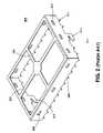
- the fence 200includes a cross bar style support 201 , 203 , which must be mechanically snipped away if a repair is required prior to the installation of a new lid.
- This type of fence 200further includes a plurality of engagement slots 205 , 207 as well as a plurality of projections 209 , 211 that engage with the PC board to hold the fence into position.
- One or more twist tabs 213are also used to provide a firm mechanical connection to portions of the PC board.
- any type of RF shieldis used in connection with outside connector-type devices used on the PC board.
- Shields that are designed for covering or providing a hoodare often referred to as a “dog house” shield and are used for isolating the pins of a connector body that provide external connections to the outside devices.
- the necessity for added holes in the PC board and the typical assembly techniques employed to attach the shield components with twist tabs prior to the solder operationadds expensive assembly time and limits the application to a leaded style component parts.
- these types of connector shieldsutilize fastening screws to mechanically provide a strain relief for the connector as well as enabling a adequate electrical ground. Thus, shields of this type also add a great deal of operational cost in view of these complex assembly requirements.
- FIG. 3Aillustrates a perspective view of connector shield 300 having a frame 301 that includes a ground slot 303 for insertion of a grounding member (not shown) that provides an electrical ground.
- a grounding tab 305 and fastening tab 307are also used to hold the connector shield to a PC board or the like.
- FIG. 3Balso illustrates a perspective view of an alternative bracket similar to that in FIG.
- a frame 309includes a ground spring 311 for making ground contract with a metallic object and one or more twist tabs 313 for grounding the frame 309 to a PC board.
- a ground spring 311for making ground contract with a metallic object
- one or more twist tabs 313for grounding the frame 309 to a PC board.
- FIG. 1is a perspective view of a shield cover as used in the prior art
- FIG. 2is a prior art diagram of the metal frame as used in the prior art
- FIGS. 3A and 3Bare perspective view of connector shield used in the prior art
- FIGS. 4A , 4 B, 4 C, and 4 Dillustrate a perspective view of the top of the elastomeric shield, bottom of the electrometric shield, top view of the elastomeric shield, and magnified view of the circular turret section, respectively, in accordance with some embodiments of the invention
- FIGS. 5A , 5 B, 5 C, and 5 Dillustrate a perspective view, a front view, a top view, and a side view, respectively, of a connector shield as used in accordance with an alternative embodiment of the invention.
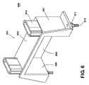
- FIG. 6illustrates a perspective view of a connector shield having an attached ground contact in accordance with an alternative embodiment of the invention.
- FIGS. 4A , 4 B, 4 C, and 4 Dillustrate a perspective view of the top of the elastomeric shield, a perspective view of the bottom of the elastomeric shield, a bottom plan view of the elastomeric shield, and a magnified view of the circular turret section, respectively, in accordance with an embodiment of the invention.
- an elastomeric shield 400incorporates an electrically conductive elastomeric material molded directly into the shield 400 in a manner such that the shield can be configured into any desired shape.
- the shield 400includes a top section 401 , underside section 403 , and edge sections 405 . At each corner of the shield 400 , a circular turret section 406 is used to hold a frictional engagement member 407 .
- the engagement member 407is oriented on the turret section 407 such that it projects away from the underside section 403 using a base 404 .
- the surface of the engagement member 407may also include ridges, bumps, hooks, and/or other means 412 for enabling the engagement member 407 to be frictionally retained within a corresponding aperture 408 on a PC board 410 .
- the shield 400is molded such that it forms an interface with one or more select holes through the PC board 408 . This configuration allows either a push-through, pull-through, or a push/pull retention with the engagement member 407 .
- the elastomeric material used in the shield 400can be manufactured of many varieties of silicone rubber or other non-conductive pliable material.
- the electrical mu-metal fillers combined with the silicone rubbermight include but is not limited to Silver (Ag), Silver/Copper (Ag/Cu), Silver/Nickel (Ag/Ni), Nickel/Graphite (Ni/Graphite), or the like.
- SilverAg
- Silver/CopperAg/Cu
- Silver/NickelAg/Ni
- Nickel/GraphiteNi/Graphite
- the advantages of the elastomeric material over the sheet metal or metalized plasticis that it is more compliant to variations in the surface of the board allowing for a better seal against a contact runner (not shown). Methods for securing the molded shield to the circuit board, will not require soldering, making it ideal for any surface mount process or stick lead during assembly.
- an elastomeric component shieldis that it greatly reduces any chance for noise, such as a mechanical rattle, that is often present when utilizing sheet metal shields. This may stem from the component, as in the cover on a soldered-style perimeter wall, or from an adjacent component, such as a ziff-style cable connector, that may vibrate against metal.
- the molded shieldeliminates the need for assembly prior to soldering as well as any twisting tabs or other mechanical fasteners in order to fasten the shield into position.
- FIGS. 5A , 5 B, 5 C, and 5 Dillustrate a perspective view, a front view, a top view, and a side view, respectively, of a connector shield as used in accordance with an alternative embodiment of the invention.
- the connector shield 500includes a housing 501 that forms a partial enclosure with a PC board (not shown).
- the housing 501includes a top 503 , sides 505 , 507 , and a back 509 .
- a skirt 511is positioned about the lower perimeter of the sides 505 , 507 and back 509 .
- the skirt 511is used to form a tighter RF seal with the PC board 510 .
- An upper flange 513extends across the upper edge of the housing 501 in order to provide an RF seal with an electrical connector (not shown), which can be placed within the housing 501 .
- the shield 500further includes one or more turrets 515 each having an engagement member 517 for frictional engagement within an associated aperture in the PC board. When access to the connector assembly is required, the shield 500 can be easily removed by providing an upward or pulling force to remove either engagement member(s) 517 from their respective apertures.
- FIG. 6illustrates a perspective view of a connector shield having an attached ground contact in accordance with an alternative embodiment of the invention.
- the shield 600includes a housing 601 that comprises a top 603 , sides 605 , 607 , and back 609 .
- One or more turrets 611 and associated respective engagement member 613are used for holding the shield into an aperture on a PC board.
- the shield 600also includes a resilient ground stub 615 for allowing the shield to make electrical contact with a chassis ground or the like.
- the resiliency of the grounding stub 615can be designed to provide a ground to the case or chassis by a compression contact for eliminating screws or other types of mechanical fasteners.
- grounding stub 615eliminates a need for twist tabs or specialized tools used in the manufacturing process.
- the grounding stub 615can be incorporated as part of the shield design in any plane that is needed to contact a case or chassis surface. This provides the capability to incorporate a dual shield in the event two circuit boards are oriented either in parallel, allowing a shield “sandwich-like” configuration or, if perpendicular, a right-angled style of interface that can be positioned to maximize the shielding potential from a single part.
- the nature and properties of the elastomeric materialalso allow for a tight RF seal of any electromagnetic charge (EMC) that provides a portal that may sometimes be needed for certain types of electrical enclosures.
- EMCelectromagnetic charge
- Another advantage to the elastomeric shield of the present inventionis that it can be attached to another electrical or mechanical component other than a printed circuit board while still providing the necessary shielding functionality to desired components.
- the push/pull nature of the engagement membercan be used on a cover such that when the cover is attached to the assembly, the elastomeric shield may include one or more ribs that seal against a printed circuit board on a ground runner.
- any interface enclosure gapscan be easily sealed due to the pliable nature of the elastomeric material.
- Multiple shields and/or shield assemblies with ground springscan also be replaced with a single mounted elastomeric shield.
- Still yet another embodiment of the inventionincludes a method for spraying the inside of the elastomeric housing with a metalized coating or with a vacuum metalized process to provide a thin layer conductive shield.
- a foil coatingcan be applied to the underside of an elastomeric body. This allows the elastomeric properties of the invention to fulfill the structure and retention capabilities of the shield for enabling the conductive part to provide the metalized shielding.
- the elastomeric shieldcan be molded in a matrix or sheet to maximize processing and handling efficiency. The characteristics of the elastomeric material allows for grooving with thin, tear-away sections allowing individual switch pads to be ripped or torn from a large sheet of shield devices segmented into individual sections.
- the present inventionis directed to an elastomeric shield for use in shielding radio frequency (RF) energy that includes at least one conductive elastomeric cover having a plurality of elastomeric sidewalls surrounding the cover.
- RFradio frequency
- One or more turretsare formed with the plurality of sidewalls for holding an engagement member where the engagement member operates to removably hold the conductive elastomeric shield into a fixed position on a printed circuit (PC) board.
- PCprinted circuit
Landscapes
- Engineering & Computer Science (AREA)
- Microelectronics & Electronic Packaging (AREA)
- Shielding Devices Or Components To Electric Or Magnetic Fields (AREA)
Abstract
Description
Claims (20)
Priority Applications (2)
| Application Number | Priority Date | Filing Date | Title |
|---|---|---|---|
| US11/983,248US7609530B2 (en) | 2007-11-08 | 2007-11-08 | Conductive elastomeric shielding device and method of forming same |
| EP08167522AEP2059108A3 (en) | 2007-11-08 | 2008-10-24 | A conductive elastomeric shielding device and method of forming same |
Applications Claiming Priority (1)
| Application Number | Priority Date | Filing Date | Title |
|---|---|---|---|
| US11/983,248US7609530B2 (en) | 2007-11-08 | 2007-11-08 | Conductive elastomeric shielding device and method of forming same |
Publications (2)
| Publication Number | Publication Date |
|---|---|
| US20090122507A1 US20090122507A1 (en) | 2009-05-14 |
| US7609530B2true US7609530B2 (en) | 2009-10-27 |
Family
ID=40436450
Family Applications (1)
| Application Number | Title | Priority Date | Filing Date |
|---|---|---|---|
| US11/983,248ActiveUS7609530B2 (en) | 2007-11-08 | 2007-11-08 | Conductive elastomeric shielding device and method of forming same |
Country Status (2)
| Country | Link |
|---|---|
| US (1) | US7609530B2 (en) |
| EP (1) | EP2059108A3 (en) |
Cited By (8)
| Publication number | Priority date | Publication date | Assignee | Title |
|---|---|---|---|---|
| US8477509B2 (en) | 2006-08-18 | 2013-07-02 | Delphi Technologies, Inc. | Lightweight audio system for automotive applications and method |
| US8526161B2 (en) | 2010-04-19 | 2013-09-03 | Apple Inc. | Button structures for electronic devices |
| US8610822B2 (en) | 2010-04-19 | 2013-12-17 | Apple Inc. | Camera alignment and mounting structures |
| US8760886B2 (en) | 2006-08-18 | 2014-06-24 | Delphi Technologies, Inc. | Lightweight audio system for automotive applications and method |
| US9237685B2 (en) | 2006-08-18 | 2016-01-12 | Delphi Technologies, Inc. | Lightweight audio system for automotive applications and method |
| USD823674S1 (en)* | 2017-06-16 | 2018-07-24 | Zmc Metal Coating Inc. | Fascia bracket for roller shade |
| US11056441B2 (en) | 2019-12-05 | 2021-07-06 | Apple Inc. | Electromagnetic shielding of compact electronic modules |
| US11303064B2 (en)* | 2020-07-10 | 2022-04-12 | Beijing Voyager Technology Co., Ltd. | Methods and apparatuses for aligning and coupling a circuit board with a chassis and another circuit board |
Families Citing this family (3)
| Publication number | Priority date | Publication date | Assignee | Title |
|---|---|---|---|---|
| EP2684435B1 (en) | 2011-03-11 | 2019-10-02 | Aptiv Technologies Limited | Flexible electronic circuit enclosure assembly |
| US8952272B2 (en)* | 2012-03-07 | 2015-02-10 | Apple Inc. | Molded EMI and thermal shield |
| US9054779B2 (en)* | 2012-09-14 | 2015-06-09 | Hewlett-Packard Development Company, L.P. | Radio frequency interference shield |
Citations (5)
| Publication number | Priority date | Publication date | Assignee | Title |
|---|---|---|---|---|
| US5373101A (en) | 1991-05-03 | 1994-12-13 | Motorola, Inc. | Electrical interconnect apparatus |
| US5550713A (en)* | 1995-09-06 | 1996-08-27 | Aironet Wireless Communications, Inc. | Electromagnetic shielding assembly for printed circuit board |
| DE19736208C1 (en) | 1997-08-20 | 1998-12-10 | Siemens Ag | Electromagnetic sealing device for screen housing and circuit board e.g. for communications apparatus |
| US6144557A (en)* | 1999-04-09 | 2000-11-07 | Lucent Technologies, Inc. | Self-locking conductive pin for printed wiring substrate electronics case |
| WO2002043456A2 (en) | 2000-11-20 | 2002-05-30 | Parker-Hannifin, Inc. | Interference mitigation through conductive thermoplastic composite materials |
- 2007
- 2007-11-08USUS11/983,248patent/US7609530B2/enactiveActive
- 2008
- 2008-10-24EPEP08167522Apatent/EP2059108A3/ennot_activeWithdrawn
Patent Citations (5)
| Publication number | Priority date | Publication date | Assignee | Title |
|---|---|---|---|---|
| US5373101A (en) | 1991-05-03 | 1994-12-13 | Motorola, Inc. | Electrical interconnect apparatus |
| US5550713A (en)* | 1995-09-06 | 1996-08-27 | Aironet Wireless Communications, Inc. | Electromagnetic shielding assembly for printed circuit board |
| DE19736208C1 (en) | 1997-08-20 | 1998-12-10 | Siemens Ag | Electromagnetic sealing device for screen housing and circuit board e.g. for communications apparatus |
| US6144557A (en)* | 1999-04-09 | 2000-11-07 | Lucent Technologies, Inc. | Self-locking conductive pin for printed wiring substrate electronics case |
| WO2002043456A2 (en) | 2000-11-20 | 2002-05-30 | Parker-Hannifin, Inc. | Interference mitigation through conductive thermoplastic composite materials |
Non-Patent Citations (2)
| Title |
|---|
| European Search Report dated Jul. 21, 2009. |
| European Search Report dated Mar. 23, 2009. |
Cited By (26)
| Publication number | Priority date | Publication date | Assignee | Title |
|---|---|---|---|---|
| US8749988B2 (en) | 2006-08-18 | 2014-06-10 | Delphi Technologies, Inc. | Lightweight audio system for automotive applications and method |
| US8625292B2 (en) | 2006-08-18 | 2014-01-07 | Delphi Technologies, Inc. | Lightweight audio system for automotive applications and method |
| US8498126B2 (en) | 2006-08-18 | 2013-07-30 | Delphi Technologies, Inc. | Lightweight audio system for automotive applications and method |
| US8760886B2 (en) | 2006-08-18 | 2014-06-24 | Delphi Technologies, Inc. | Lightweight audio system for automotive applications and method |
| US8570757B2 (en) | 2006-08-18 | 2013-10-29 | Delphi Technologies, Inc. | Lightweight audio system for automotive applications and method |
| US8593821B2 (en) | 2006-08-18 | 2013-11-26 | Delphi Technologies, Inc. | Lightweight audio system for automotive applications and method |
| US8599568B2 (en) | 2006-08-18 | 2013-12-03 | Delphi Technologies, Inc. | Lightweight audio system for automotive applications and method |
| US8477509B2 (en) | 2006-08-18 | 2013-07-02 | Delphi Technologies, Inc. | Lightweight audio system for automotive applications and method |
| US8625293B2 (en) | 2006-08-18 | 2014-01-07 | Delphi Technologies, Inc. | Lightweight audio system for automotive applications and method |
| US9173332B2 (en) | 2006-08-18 | 2015-10-27 | Delphi Technologies, Inc. | Lightweight audio system for automotive applications and method |
| US8724335B2 (en) | 2006-08-18 | 2014-05-13 | Delphi Technologies, Inc. | Lightweight audio system for automotive applications and method |
| US8731862B2 (en) | 2006-08-18 | 2014-05-20 | Delphi Technologies, Inc. | Lightweight audio system for automotive applications and method |
| US8493739B2 (en) | 2006-08-18 | 2013-07-23 | Delphi Technologies, Inc. | Lightweight audio system for automotive applications and method |
| US9237685B2 (en) | 2006-08-18 | 2016-01-12 | Delphi Technologies, Inc. | Lightweight audio system for automotive applications and method |
| US9013881B2 (en) | 2006-08-18 | 2015-04-21 | Delphi Technologies, Inc. | Lightweight audio system for automotive applications and method |
| US8947860B2 (en) | 2006-08-18 | 2015-02-03 | Delphi Technologies, Inc. | Lightweight audio system for automotive applications and method |
| US9237683B2 (en) | 2006-08-18 | 2016-01-12 | Delphi Technologies, Inc. | Lightweight audio system for automotive applications and method |
| US8982561B2 (en) | 2006-08-18 | 2015-03-17 | Delphi Technologies, Inc. | Lightweight audio system for automotive applications and method |
| US8830687B2 (en) | 2006-08-18 | 2014-09-09 | Delphi Technologies, Inc. | Lightweight audio system for automotive applications and method |
| US8610822B2 (en) | 2010-04-19 | 2013-12-17 | Apple Inc. | Camera alignment and mounting structures |
| US8964352B2 (en) | 2010-04-19 | 2015-02-24 | Apple Inc. | Mounting structures for components in electronic devices |
| US8526161B2 (en) | 2010-04-19 | 2013-09-03 | Apple Inc. | Button structures for electronic devices |
| US10290441B2 (en) | 2010-04-19 | 2019-05-14 | Apple Inc. | Button structures for electronic devices |
| USD823674S1 (en)* | 2017-06-16 | 2018-07-24 | Zmc Metal Coating Inc. | Fascia bracket for roller shade |
| US11056441B2 (en) | 2019-12-05 | 2021-07-06 | Apple Inc. | Electromagnetic shielding of compact electronic modules |
| US11303064B2 (en)* | 2020-07-10 | 2022-04-12 | Beijing Voyager Technology Co., Ltd. | Methods and apparatuses for aligning and coupling a circuit board with a chassis and another circuit board |
Also Published As
| Publication number | Publication date |
|---|---|
| EP2059108A2 (en) | 2009-05-13 |
| EP2059108A3 (en) | 2009-08-26 |
| US20090122507A1 (en) | 2009-05-14 |
Similar Documents
| Publication | Publication Date | Title |
|---|---|---|
| US7609530B2 (en) | Conductive elastomeric shielding device and method of forming same | |
| US8672710B2 (en) | Gasket with fingers for RJ45 cable connector | |
| KR100451291B1 (en) | Faraday cage | |
| US5175395A (en) | Electromagnetic shield | |
| EP1951021B1 (en) | Electromagnetic interference shielding apparatus and methods of making the same | |
| US7317618B2 (en) | Combined board level shielding and thermal management | |
| US7663895B2 (en) | Electromagnetic shielding device for printed circuit board | |
| US20140153192A1 (en) | Module cage with integrated emi aspect | |
| US9332680B2 (en) | Electrical gasket and electronic module having electrical gasket | |
| US6985366B2 (en) | EMC shield and housing for electronic components | |
| KR20160018236A (en) | Printed board assembly and manufacturing method thereof | |
| US20090268420A1 (en) | Shielding assembly | |
| US10010016B2 (en) | Shield can device for shielding electromagnetic wave | |
| CN104869796A (en) | Fastening structure for shield can | |
| US20120031661A1 (en) | Electromagnetic shielding device | |
| US9496656B2 (en) | Conductive attachment for shielding radiation | |
| US5438160A (en) | Sealed, shielded and filtered header receptacle | |
| US20120217051A1 (en) | Shielding assembly | |
| US6707675B1 (en) | EMI containment device and method | |
| CN107396621A (en) | Electromagnetic shield for electronic installation | |
| KR20160072758A (en) | Electric terminal contact | |
| CN107018645A (en) | Shielding construction, shielding construction preparation method, circuit module and mobile electronic terminal | |
| KR100759344B1 (en) | Interference-shielded mobile station and a corresponding method and arrangement in the interference shielding of a mobile station | |
| US9313934B2 (en) | Dispensible electrical gasket, electronic module having dispensible electrical gasket, and method of fabricating same | |
| CN111491439A (en) | Circuit board assembly and electronic equipment |
Legal Events
| Date | Code | Title | Description |
|---|---|---|---|
| AS | Assignment | Owner name:DELPHI TECHNOLOGIES, INC., MICHIGAN Free format text:ASSIGNMENT OF ASSIGNORS INTEREST;ASSIGNOR:SNIDER, CHRIS R.;REEL/FRAME:020149/0681 Effective date:20071023 | |
| STCF | Information on status: patent grant | Free format text:PATENTED CASE | |
| FPAY | Fee payment | Year of fee payment:4 | |
| FPAY | Fee payment | Year of fee payment:8 | |
| AS | Assignment | Owner name:APTIV TECHNOLOGIES LIMITED, BARBADOS Free format text:ASSIGNMENT OF ASSIGNORS INTEREST;ASSIGNOR:DELPHI TECHNOLOGIES INC.;REEL/FRAME:047143/0874 Effective date:20180101 | |
| MAFP | Maintenance fee payment | Free format text:PAYMENT OF MAINTENANCE FEE, 12TH YEAR, LARGE ENTITY (ORIGINAL EVENT CODE: M1553); ENTITY STATUS OF PATENT OWNER: LARGE ENTITY Year of fee payment:12 | |
| AS | Assignment | Owner name:APTIV TECHNOLOGIES (2) S.A R.L., LUXEMBOURG Free format text:ENTITY CONVERSION;ASSIGNOR:APTIV TECHNOLOGIES LIMITED;REEL/FRAME:066746/0001 Effective date:20230818 Owner name:APTIV MANUFACTURING MANAGEMENT SERVICES S.A R.L., LUXEMBOURG Free format text:MERGER;ASSIGNOR:APTIV TECHNOLOGIES (2) S.A R.L.;REEL/FRAME:066566/0173 Effective date:20231005 Owner name:APTIV TECHNOLOGIES AG, SWITZERLAND Free format text:ASSIGNMENT OF ASSIGNORS INTEREST;ASSIGNOR:APTIV MANUFACTURING MANAGEMENT SERVICES S.A R.L.;REEL/FRAME:066551/0219 Effective date:20231006 |