US7609331B2 - Method of manufacturing array substrate for liquid crystal display device - Google Patents
Method of manufacturing array substrate for liquid crystal display deviceDownload PDFInfo
- Publication number
- US7609331B2 US7609331B2US11/643,977US64397706AUS7609331B2US 7609331 B2US7609331 B2US 7609331B2US 64397706 AUS64397706 AUS 64397706AUS 7609331 B2US7609331 B2US 7609331B2
- Authority
- US
- United States
- Prior art keywords
- layer
- gate
- amorphous silicon
- metal layer
- photoresist pattern
- Prior art date
- Legal status (The legal status is an assumption and is not a legal conclusion. Google has not performed a legal analysis and makes no representation as to the accuracy of the status listed.)
- Expired - Lifetime, expires
Links
Images


Classifications
- G—PHYSICS
- G02—OPTICS
- G02F—OPTICAL DEVICES OR ARRANGEMENTS FOR THE CONTROL OF LIGHT BY MODIFICATION OF THE OPTICAL PROPERTIES OF THE MEDIA OF THE ELEMENTS INVOLVED THEREIN; NON-LINEAR OPTICS; FREQUENCY-CHANGING OF LIGHT; OPTICAL LOGIC ELEMENTS; OPTICAL ANALOGUE/DIGITAL CONVERTERS
- G02F1/00—Devices or arrangements for the control of the intensity, colour, phase, polarisation or direction of light arriving from an independent light source, e.g. switching, gating or modulating; Non-linear optics
- G02F1/01—Devices or arrangements for the control of the intensity, colour, phase, polarisation or direction of light arriving from an independent light source, e.g. switching, gating or modulating; Non-linear optics for the control of the intensity, phase, polarisation or colour
- G02F1/13—Devices or arrangements for the control of the intensity, colour, phase, polarisation or direction of light arriving from an independent light source, e.g. switching, gating or modulating; Non-linear optics for the control of the intensity, phase, polarisation or colour based on liquid crystals, e.g. single liquid crystal display cells
- G02F1/133—Constructional arrangements; Operation of liquid crystal cells; Circuit arrangements
- G02F1/1333—Constructional arrangements; Manufacturing methods
- G02F1/1345—Conductors connecting electrodes to cell terminals
- G02F1/13458—Terminal pads
- G—PHYSICS
- G02—OPTICS
- G02F—OPTICAL DEVICES OR ARRANGEMENTS FOR THE CONTROL OF LIGHT BY MODIFICATION OF THE OPTICAL PROPERTIES OF THE MEDIA OF THE ELEMENTS INVOLVED THEREIN; NON-LINEAR OPTICS; FREQUENCY-CHANGING OF LIGHT; OPTICAL LOGIC ELEMENTS; OPTICAL ANALOGUE/DIGITAL CONVERTERS
- G02F1/00—Devices or arrangements for the control of the intensity, colour, phase, polarisation or direction of light arriving from an independent light source, e.g. switching, gating or modulating; Non-linear optics
- G02F1/01—Devices or arrangements for the control of the intensity, colour, phase, polarisation or direction of light arriving from an independent light source, e.g. switching, gating or modulating; Non-linear optics for the control of the intensity, phase, polarisation or colour
- G02F1/13—Devices or arrangements for the control of the intensity, colour, phase, polarisation or direction of light arriving from an independent light source, e.g. switching, gating or modulating; Non-linear optics for the control of the intensity, phase, polarisation or colour based on liquid crystals, e.g. single liquid crystal display cells
- G02F1/133—Constructional arrangements; Operation of liquid crystal cells; Circuit arrangements
- G02F1/1333—Constructional arrangements; Manufacturing methods
- G—PHYSICS
- G02—OPTICS
- G02F—OPTICAL DEVICES OR ARRANGEMENTS FOR THE CONTROL OF LIGHT BY MODIFICATION OF THE OPTICAL PROPERTIES OF THE MEDIA OF THE ELEMENTS INVOLVED THEREIN; NON-LINEAR OPTICS; FREQUENCY-CHANGING OF LIGHT; OPTICAL LOGIC ELEMENTS; OPTICAL ANALOGUE/DIGITAL CONVERTERS
- G02F1/00—Devices or arrangements for the control of the intensity, colour, phase, polarisation or direction of light arriving from an independent light source, e.g. switching, gating or modulating; Non-linear optics
- G02F1/01—Devices or arrangements for the control of the intensity, colour, phase, polarisation or direction of light arriving from an independent light source, e.g. switching, gating or modulating; Non-linear optics for the control of the intensity, phase, polarisation or colour
- G02F1/13—Devices or arrangements for the control of the intensity, colour, phase, polarisation or direction of light arriving from an independent light source, e.g. switching, gating or modulating; Non-linear optics for the control of the intensity, phase, polarisation or colour based on liquid crystals, e.g. single liquid crystal display cells
- G02F1/133—Constructional arrangements; Operation of liquid crystal cells; Circuit arrangements
- G02F1/136—Liquid crystal cells structurally associated with a semi-conducting layer or substrate, e.g. cells forming part of an integrated circuit
- G02F1/1362—Active matrix addressed cells
- G02F1/136227—Through-hole connection of the pixel electrode to the active element through an insulation layer
- G—PHYSICS
- G02—OPTICS
- G02F—OPTICAL DEVICES OR ARRANGEMENTS FOR THE CONTROL OF LIGHT BY MODIFICATION OF THE OPTICAL PROPERTIES OF THE MEDIA OF THE ELEMENTS INVOLVED THEREIN; NON-LINEAR OPTICS; FREQUENCY-CHANGING OF LIGHT; OPTICAL LOGIC ELEMENTS; OPTICAL ANALOGUE/DIGITAL CONVERTERS
- G02F1/00—Devices or arrangements for the control of the intensity, colour, phase, polarisation or direction of light arriving from an independent light source, e.g. switching, gating or modulating; Non-linear optics
- G02F1/01—Devices or arrangements for the control of the intensity, colour, phase, polarisation or direction of light arriving from an independent light source, e.g. switching, gating or modulating; Non-linear optics for the control of the intensity, phase, polarisation or colour
- G02F1/13—Devices or arrangements for the control of the intensity, colour, phase, polarisation or direction of light arriving from an independent light source, e.g. switching, gating or modulating; Non-linear optics for the control of the intensity, phase, polarisation or colour based on liquid crystals, e.g. single liquid crystal display cells
- G02F1/133—Constructional arrangements; Operation of liquid crystal cells; Circuit arrangements
- G02F1/136—Liquid crystal cells structurally associated with a semi-conducting layer or substrate, e.g. cells forming part of an integrated circuit
- G02F1/1362—Active matrix addressed cells
- G02F1/136231—Active matrix addressed cells for reducing the number of lithographic steps
- G02F1/136236—Active matrix addressed cells for reducing the number of lithographic steps using a grey or half tone lithographic process
Definitions
- the present inventionrelates to a liquid crystal display (LCD) device and more particularly, to a method of manufacturing an array substrate for the liquid crystal display device.
- LCDliquid crystal display
- a liquid crystal display (LCD) devicein general, includes two substrates, which are spaced apart and facing each other, and a liquid crystal layer interposed between the two substrates.
- Each of the substratesincludes an electrode, and the electrodes of each substrate are also facing each other. Voltage is applied to each electrode, and thus an electric field is induced between the electrodes. Alignment of the liquid crystal molecules is changed by the varying intensity or direction of the electric field.
- the LCD devicedisplays a picture by varying transmissivity of the light varying according to the arrangement of the liquid crystal molecules.
- FIG. 1is an exploded perspective view illustrating a conventional LCD device.
- the conventional LCD device 1has upper and lower substrates 5 and 22 , which are spaced apart from and facing each other, and also has liquid crystal 15 interposed between the upper substrate 5 and the lower substrate 22 .
- the upper substrate 5includes a black matrix 6 , a color filter layer 7 , and a common electrode 9 subsequently on the inside (i.e., the side facing the lower substrate 22 ).
- the black matrix 6has an opening.
- the color filter layer 7corresponds to openings in the black matrix 6 and includes three sub-color filters of red (R), green (G), and blue (B).
- the common electrode 9is formed on the color filter 7 and is transparent.
- At least one gate line 12 and at least one data line 34are formed on the inner surface of the lower substrate 22 (i.e., the side facing the upper substrate 5 ).
- the gate line 12 and the date line 34cross each other to define a pixel area P.
- a thin film transistor Tas a switching element, is formed at the crossing of the gate line 12 and the data line 34 .
- the thin film transistor Tincludes a gate electrode, a source electrode and a drain electrode. A plurality of such thin film transistors is arranged in a matrix from to correspond to other crossings of gate and data lines.
- a pixel electrode 56which is connected to the thin film transistor T, is formed in the pixel area P.
- the pixel electrode 56corresponds to the sub-color filter, and is made of a transparent conductive material such as indium-tin-oxide (ITO) that transmits light relatively well.
- the lower substrate 22which includes the thin film transistors T and the pixel electrodes 56 arranged in the matrix form, may be commonly referred to as an array substrate.
- a scanning pulseis applied to the gate electrode of the thin film transistor T through the gate line 12 and a data signal is applied to the source electrode of the thin film transistor T through the data line 34 .
- the LCD deviceis driven due to electrical and optical effects of the liquid crystal.
- the liquid crystalis dielectric anisotropic material having a property of spontaneous polarization. When a voltage is applied, the liquid crystal forms a dipole by the spontaneous polarization, and thus molecules of the liquid crystal are arranged by an electric field.
- Optical modulationoccurs from the optical properties of the liquid crystal, which vary according to the arrangement of the liquid crystal. Images of the LCD device are produced by controlling transmittance of the light due to the optical modulation.
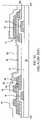
- FIG. 2illustrates a plan view of an array substrate for a LCD device according to the related art.
- a gate line 12 and a data line 34cross each other and define a pixel area P.
- a thin film transistor Tis formed as a switching element at the crossing of the gate and data lines 12 and 34 .
- a gate pad 10is formed at one end of the gate line 12
- a data pad 36is formed at one end of the data line 34 .
- a gate pad terminal 58 and a data pad terminal 60which have an island shape and are made of a transparent conducting material, overlap the gate pad 10 and the data pad 36 , respectively.
- the thin film transistor Tincludes a gate electrode 14 that is connected to the gate line 12 and receives scanning signals, a source electrode 40 that is connected to the data line 34 and receives data signals, and a drain electrode 42 that is spaced apart from the source electrode 40 .
- the thin film transistor Tfurther includes an active layer 32 between the gate electrode 14 and the source and drain electrodes 40 and 42 .
- a metal pattern 38 of an island shapeoverlaps the gate line 12 .
- a pixel electrode 56is formed in the pixel area P and is connected to the drain electrode 42 .
- the pixel electrode 56is also connected to the metal pattern 38 .
- the gate line 12 and the metal pattern 38function as first and second storage capacitor electrodes, respectively, and form a storage capacitor Cst with a gate insulating layer (not shown) disposed between the gate line 12 and the metal pattern 38 .
- an ohmic contact layeris formed between the active layer 32 and the source and drain electrodes 40 and 42 .
- the active layer 32is made of amorphous silicon
- the ohmic contact layeris formed of a doped amorphous silicon.
- a first pattern 35 and a second pattern 39which include the amorphous silicon and the doped amorphous silicon, are formed under the data line 34 and the metal pattern 38 , respectively.
- the array substrate of FIG. 2is fabricated using four masks.
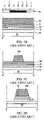
- FIGS. 3A to 3G , FIGS. 4A to 4G , and FIGS. 5A to 5Gillustrate manufacturing processes of an array substrate using four masks, and correspond to cross-sections along the line III-III, the line IV-IV, and the line V-V of FIG. 2 , respectively.
- a gate line 12 , a gate electrode 14 and a gate pad 10are formed on a transparent insulating substrate 22 by depositing a first metal layer and patterning the first metal layer through a first photolithography process using a first mask.
- the gate line 12 , the gate electrode 14 and the gate pad 10are made of a metal material such as aluminum (Al), an aluminum alloy, molybdenum (Mo), tungsten (W), and chromium (Cr).
- the gate line 12 , the gate electrode 14 and the gate pad 10 made of aluminum or aluminum alloymay be formed of a double layer including molybdenum or chromium.
- a gate insulating layer 16 , an amorphous silicon layer 18 , a doped amorphous silicon layer 20 and a second metal layer 24are subsequently deposited on the substrate 22 including the gate line 12 , the gate electrode 14 and the gate pad 10 thereon.
- the gate insulating layer 16is made of an inorganic insulating material such as silicon nitride (SiNx) and silicon oxide (SiO 2 ), and the second metal material 24 is formed of one of chromium, molybdenum, tungsten and tantalum (Ta).
- a photoresist layer 26is formed on the second metal layer 24 by coating photoresist.
- a second mask 50which has a transmitting portion A, a blocking portion B and a half transmitting portion C, is disposed over the photoresist layer 26 spacing apart.
- the half transmitting portion Ccorresponds to the gate electrode 14 .
- the photoresist layer 26may be a positive type, and a portion exposed to light is developed and removed. Subsequently, the photoresist layer 26 is exposed to light.
- the photoresist layer 26 corresponding to the half transmitting portion Cis exposed less than the photoresist layer 26 corresponding to the transmitting portion A.
- the exposed photoresist layer 26 of FIGS. 3B , 4 B and 5 Bis developed, and a photoresist pattern 26 a is formed. Because of the different transmittances of the portions of the second mask 50 , the photoresist pattern 26 a has different thicknesses. A first thickness of the photoresist pattern 26 a corresponds to the blocking portion B of FIGS. 3B , 4 B and 5 B and a second thickness of the photoresist pattern 26 a , which is thinner than the first thickness, corresponds to the half transmitting portion C of FIGS. 3B , 4 B and 5 B.
- the second metal layer 24 , the doped amorphous silicon layer 20 and the amorphous silicon layer 18 of FIGS. 3C , 4 C and 5 C exposed by the photoresist pattern 26 aare removed.
- a source and drain pattern 28 , a data line 34 of FIG. 2 , a data pad 36 , a doped amorphous silicon pattern 30 a , and an active layer 32are formed.
- the second metal layer 24 of FIGS. 3C , 4 C and 5 Cis etched by a wet etching method, and the doped amorphous silicon layer 20 and the amorphous silicon layer 18 of FIGS.
- the source and drain pattern 28is formed over the gate electrode 14 , and is connected to a data line 34 of FIG. 2 , which extends vertically in the context of the figure.
- the doped amorphous silicon pattern 30 a and the active layer 32have the same shape as the source and drain pattern 28 and the data line 34 .
- a metal pattern 38 of an island shapeis also formed over the gate line 12 .
- a first pattern 35 and a second pattern 39which include the amorphous silicon layer and the doped amorphous silicon layer, are formed.
- the first pattern 35is located under the data line (not shown) and the data pad 36 and the second pattern 39 is situated under the metal pattern 38 .
- the second thickness of the photoresist pattern 26 ais removed through an ashing process, and thus the source and drain pattern 28 is exposed.
- the photoresist pattern 26 a of the first thicknessis also removed partially and the first thickness of the photoresist pattern 26 a is thinned. Additionally, edges of the photoresist pattern 26 a are removed, and the metal patterns 28 , 36 and 38 are exposed.
- the source and drain pattern 28 and the doped amorphous silicon pattern 30 a of FIG. 3Ewhich are exposed by the photoresist pattern 26 a of FIG. 3E , are etched.
- source and drain electrodes 40 and 42 and an ohmic contact layer 30are formed, and the active layer 32 is exposed.
- the exposed active layer 32 between the source and drain electrodes 40 and 42becomes a channel of a thin film transistor.
- the source and drain electrodes 40 and 42are spaced apart from each other. A region between the source and drain electrodes 40 and 42 corresponds to the half transmitting portion C of the second mask 50 of FIG. 3B . If the source and drain pattern 28 of FIG.
- 3Eis formed of molybdenum (Mo), the source and drain pattern 28 and the doped amorphous silicon pattern 30 a of FIG. 3E can be removed using the dry etching method at one time. However, if the source and drain pattern 28 is formed of chromium (Cr), the source and drain pattern 28 is etched by the wet etching method, and then the doped amorphous silicon pattern 30 a is removed by the dry etching method.
- Momolybdenum
- Crchromium
- the source and drain electrodes 40 and 42 , the data line 34 , the data pad 36 , the metal pattern 38 , the ohmic contact layer 30 and the active layer 32are formed through a second photolithography process using the second mask of FIGS. 3B , 4 B and 5 B.
- a passivation layer 46is formed on the data line 34 , the source and drain electrodes 40 and 42 , the data pad 36 , and the metal pattern 38 by coating a transparent organic material such as benzocyclobutene (BCB) and acrylic resin or depositing an inorganic material such as silicon nitride (SiNx) and silicon oxide (SiO 2 ).
- the passivation layer 46is patterned with the gate electrode 16 through a third photolithography process using a third mask, and a drain contact hole 48 , a storage contact hole 51 , a gate pad contact hole 52 and a data pad contact hole 54 are formed.
- the drain contact hole 48 , the storage contact hole 51 , the gate pad contact hole 52 and the data pad contact hole 54expose the drain electrode 42 , the metal pattern 38 , the gate pad 10 and the data pad 36 , respectively.
- the storage contact hole 51exposes a sidewall of the metal pattern 38 .
- a pixel electrode 56 , a gate pad terminal 58 and a data pad terminal 60are formed on the passivation layer 46 by depositing a transparent conductive material such as indium-tin-oxide (ITO) and indium-zinc-oxide (IZO) and patterning the transparent conductive material through a fourth photolithography process using a fourth mask.
- the pixel electrode 56is connected to not only the drain electrode 42 via the drain contact hole 48 but also to the metal pattern 38 through the storage contact hole 51 .
- the gate pad terminal 58 and the data pad terminal 60are connected to the gate pad 10 and the data pad 36 , respectively.
- the array substrateis manufactured through photolithography processes using a mask.
- the photolithography processincludes several steps of cleaning, coating a photo-resist layer, exposing through a mask, developing the photo-resist layer, and etching. Therefore, fabricating time, costs, and failure may be decreased by reducing the number of the photolithography process.
- the present inventionis directed to a manufacturing method of an array substrate for a liquid crystal display device that substantially obviates one or more of problems due to limitations and disadvantages of the related art.
- An advantage of the present inventionis to provide a manufacturing method of an array substrate for a liquid crystal display device that increases productivity because of the shorter processes and the lower cost.
- a method of manufacturing an array substrate for a liquid crystal display deviceincludes the steps of forming a gate line, a gate pad and a gate electrode on a substrate, forming a gate insulating layer on the gate line, the gate electrode and the gate pad, forming an active layer on the gate insulating layer, forming an ohmic contact layer on the active layer, forming a data line, a data pad, and source and drain electrodes on the ohmic contact layer, forming a pixel electrode on the source and drain electrodes, the pixel electrode contacting the drain electrode, forming a first passivation layer on the substrate including the pixel electrode, forming a second passivation layer on the first passivation layer, the second passivation layer exposing the first passivation layer over the gate pad and the data pad, and patterning the first passivation layer exposed by the second passivation layer to expose the gate pad and the data pad.
- a method of manufacturing an array substrate for a liquid crystal display deviceincludes the steps of depositing a first metal layer on a transparent substrate; patterning the first metal layer to form a gate line; a gate electrode; and a gate pad; forming a gate insulating layer over the transparent substrate and the patterned first metal layer; depositing a doped amorphous silicon layer and a second metal layer over the gate insulating layer; providing a photoresist pattern having first and second thicknesses over the second metal layer; selectively removing portions of the second metal layer according to the photoresist pattern; selectively removing portions of the amorphous silicon layer according to the photoresist pattern and selectively etching the gate insulating layer according to the photoresist pattern; removing a portion of the photoresist pattern having the first thickness; selectively etching the second metal layer exposed by removing the portion of the photoresist pattern having the first thickness; selectively etching the doped amorphous silicon layer exposed by selectively
- FIG. 1is an exploded perspective view illustrating a related art liquid crystal display (LCD) device
- FIG. 2is a plan view illustrating an array substrate for a LCD device according to the related art
- FIGS. 3A to 3G , FIGS. 4A to 4G , and FIGS. 5A to 5Gare cross-sectional views illustrating manufacturing method of an array substrate according to the related art
- FIG. 6is a plan view illustrating an array substrate for a liquid crystal display (LCD) device according to an embodiment of the present invention.
- FIGS. 7A to 7H , FIGS. 8A to 8H , and FIGS. 9A to 9Hare cross-sectional views illustrating a manufacturing of an array substrate corresponding to the present invention.
- FIG. 6is a plan view of an array substrate for a liquid crystal display (LCD) device according to an embodiment of the present invention.
- LCDliquid crystal display
- a gate line 112 and a data line 134are formed on a transparent insulating substrate 100 .
- the gate line 112 and the data line 134cross each other and define a pixel area P.
- a thin film transistor Tis formed as a switching element at the crossing of the gate and data lines 112 and 134 .
- a gate pad 110is formed at one end of the gate line 112 and a data pad 136 is formed at one end of the data line 134 .
- a gate pad terminal 148 and a data pad terminal 150which have an island shape and are made of a transparent conducting material, overlap the gate pad 110 and the data pad 136 , respectively.
- the thin film transistor Tis composed of a gate electrode 114 that is connected to the gate line 112 for receiving scanning signals, a source electrode 140 that is connected to the data line 134 for receiving data signals, and a drain electrode 142 that spaces apart from the source electrode 140 .
- the thin film transistor Tfurther includes an active layer 132 between the gate electrode 114 and the source and drain electrodes 140 and 142 .
- a metal material 138overlaps the gate line 112 .
- the metal material 138may be made of the same material as the data line 134 .
- a pixel electrode 146is formed in the pixel area P.
- the pixel electrode 146is connected to the drain electrode 142 and the metal pattern 138 with side contact.
- the gate line 112 and the metal pattern 138function as first and second storage capacitor electrodes, respectively, and form a storage capacitor Cst with a gate insulating layer (not shown) disposed between the gate line 112 and the metal pattern 138 .
- a transparent organic layer 154is formed in a region except for the gate pad 110 and the data pad 136 .
- an ohmic contact layeris formed between the active layer 132 and the source and drain electrodes 140 and 142 .
- the active layer 132is made of amorphous silicon
- the ohmic contact layeris formed of a doped amorphous silicon.
- a first pattern 135 and a second pattern 139which include the amorphous silicon and the doped amorphous silicon, are formed under the data line 134 and the metal pattern 138 , respectively.
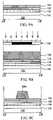
- FIGS. 7A to 7H , FIGS. 8A to 8H , and FIGS. 9A to 9Hillustrate a method of manufacturing an array substrate corresponding to the present invention, and are cross-sections along the line VII-VII, the line VIII-VIII and the line IX-IX of FIG. 6 , respectively.
- a gate line 112 , a gate electrode 114 , and a gate pad 110are formed on a transparent insulating substrate 100 by depositing a first metal layer and patterning the first metal layer through a first photolithography process using a first mask.
- the gate electrode 114is extended from the gate line 112 , and the gate pad 110 is situated at one end of the gate line 112 .
- aluminum (Al)which has a relatively low resistivity, is widely used as a gate electrode material.
- pure aluminumis easily corroded by acid and may cause line defects due to hillocks in the following process under high temperatures. Therefore, an aluminum alloy may be used or a double layer including aluminum and other metal material, such as molybdenum.
- a gate insulating layer 116is deposited on the substrate 100 including the gate line 112 , the gate electrode 114 and the gate pad 110 thereon.
- the gate insulating layer 116is made of an inorganic insulating material such as silicon nitride (SiNx) and silicon oxide (SiO 2 ).
- the gate insulating layer 116may be formed of an organic insulating material such as benzocyclobutene (BCB) and acrylic resin.
- the second metal layer 124is made of one of chromium, molybdenum, tungsten and tantalum (Ta).
- a photoresist layer 126is formed on the second metal layer 124 by coating photoresist.
- a second mask 150which has a transmitting portion E, a blocking portion F and a half transmitting portion G, is disposed over and spaced apart from the photoresist layer 126 .
- the half transmitting portion Gmay include slits and corresponds to a channel of a thin film transistor.
- the photoresist layer 126may be a positive type, and thus a portion exposed to light is developed and removed. Subsequently, the photoresist layer 126 is exposed to light, and the photoresist layer 126 corresponding to the half transmitting portion G is exposed less than the photoresist layer 126 corresponding to the transmitting portion E.
- the photoresist layer 126 of FIGS. 7B , 8 B and 9 Bis developed, and a photoresist pattern 126 a having different thicknesses is formed.
- a first thickness of the photoresist pattern 126 acorresponds to the blocking portion F of FIGS. 7B , 8 B and 9 B
- a second thickness of the photoresist pattern 126 awhich is thinner than the first thickness, corresponds to the half transmitting portion G of FIG. 7B .
- the second metal layer 124 , the doped amorphous silicon layer 120 and the amorphous silicon layer 118 of FIGS. 7C , 8 C and 9 C exposed by the photoresist pattern 126 aare removed.
- a source and drain pattern 128 , a data line 134 of FIG. 6 , a data pad 136 , a doped amorphous silicon pattern 130 a and an active layer 132are formed.
- the second metal layer 124 of FIGS. 7C , 8 C and 9 Cis etched by a wet etching method, and the doped amorphous silicon layer 120 and the amorphous silicon layer 118 FIGS.
- the source and drain pattern 128is formed over the gate electrode 114 and is connected to a data line 134 of FIG. 6 , which extends vertically in the context of the figure.
- the doped amorphous silicon pattern 130 a and the active layer 132have the same shape as the source and drain pattern 128 and the data line 134 .
- a metal pattern 138 of an island shapeis also formed over the gate line 112 .
- a first pattern 135 and a second pattern 139which include the amorphous silicon layer and the doped amorphous silicon layer, are formed.
- the first pattern 135is located under the data line (not shown) and the data pad 136 and the second pattern 139 is situated under the metal pattern 138 .
- the gate insulating layer 116is also etched, and the substrate 110 and the gate pad 110 may be exposed.
- the second thickness of the photoresist pattern 126 ais removed through an ashing process, and thus the source and drain pattern 128 is exposed.
- the first thickness of the photoresist pattern 126 ais also removed partially and the first thickness of the photoresist pattern 126 a is thinned. Additionally, edges of the photoresist pattern 126 a are removed, and the metal patterns 128 , 136 and 138 are exposed.
- the source and drain pattern 128 and the doped amorphous silicon pattern 130 a of FIG. 7Ewhich are exposed by the photoresist pattern 126 a of FIG. 7E , are etched.
- source and drain electrodes 140 and 142 and an ohmic contact layer 130are formed, and the active layer 132 is exposed.
- the exposed active layer 132 between the source and drain electrode 140 and 142becomes a channel of a thin film transistor and corresponds to the half transmitting portion G of the second mask 150 of FIG. 7B .
- the source and drain electrodes 140 and 142are spaced apart from each other. If the source and drain pattern 128 of FIG.
- the source and drain pattern 128 and the doped amorphous silicon pattern 130 a of FIG. 3Ecan be removed using the dry etching method at one time. However, if the source and drain pattern 128 is formed of chromium (Cr), the source and drain pattern 128 is etched by the wet etching method, and then the doped amorphous silicon pattern 130 a is removed by the dry etching method.
- Momolybdenum
- Crchromium
- the source and drain electrodes 140 and 142 , the data line 134 , the data pad 136 , the metal pattern 138 , the ohmic contact layer 130 and the active layer 132are formed through a second mask process using the second mask 150 of FIGS. 7B , 8 B and 9 B.
- the photoresist pattern 126 ais removed, and a pixel electrode 146 , a gate pad terminal 148 and a data pad terminal 160 are formed on the substrate 100 including the source and drain electrodes 140 and 142 by depositing a transparent conductive material such as indium-tin-oxide (ITO) and indium-zinc-oxide (IZO) and patterning the transparent conductive material through a third photolithography process using a third mask.
- the pixel electrode 146is connected to not only the drain electrode 142 but also the metal pattern 138 with side contacts.
- the gate pad terminal 148 and the data pad terminal 160are in contact with the gate pad 110 and the data pad 136 , respectively.
- a first passivation layer 152is formed on the pixel electrode 146 , the gate pad terminal 148 and the data pad terminal 150 by depositing an inorganic material such as silicon nitride (SiNx) and silicon oxide (SiO 2 ) under the temperature of about 300 degrees Celsius.
- the first passivation layer 152has a thickness within a range of about 500 ⁇ to about 1,000 ⁇ .
- the first passivation layer 152 of the inorganic insulating materialis better than an organic insulating material in contacting the active layer.
- a second passivation layer 154is formed on the first passivation layer 152 except for the gate pad 110 and the data pad 136 by printing a transparent organic material.
- the transparent organic materialmay be made of polyimide, for example.
- the first passivation layer 154 exposed by the second passivation layer 156is dry-etched.
- the second passivation layer 154may be used as an alignment layer by rubbing a surface of the second passivation layer 154 .
- the array substrate of the present inventionis manufactured by using three masks. Therefore, the manufacturing method of the array substrate according to the present invention decreases the processes and the cost, and increases productivity.
Landscapes
- Physics & Mathematics (AREA)
- Nonlinear Science (AREA)
- Mathematical Physics (AREA)
- Chemical & Material Sciences (AREA)
- Crystallography & Structural Chemistry (AREA)
- General Physics & Mathematics (AREA)
- Optics & Photonics (AREA)
- Engineering & Computer Science (AREA)
- Microelectronics & Electronic Packaging (AREA)
- Liquid Crystal (AREA)
- Thin Film Transistor (AREA)
- Devices For Indicating Variable Information By Combining Individual Elements (AREA)
Abstract
Description
Claims (23)
Priority Applications (1)
| Application Number | Priority Date | Filing Date | Title |
|---|---|---|---|
| US11/643,977US7609331B2 (en) | 2002-04-16 | 2006-12-22 | Method of manufacturing array substrate for liquid crystal display device |
Applications Claiming Priority (4)
| Application Number | Priority Date | Filing Date | Title |
|---|---|---|---|
| KR10-2002-0020724AKR100436181B1 (en) | 2002-04-16 | 2002-04-16 | method for fabricating of an array substrate for a liquid crystal display device |
| KR2002-20724 | 2002-04-16 | ||
| US10/412,321US7199846B2 (en) | 2002-04-16 | 2003-04-14 | Method of manufacturing array substrate for liquid crystal display device |
| US11/643,977US7609331B2 (en) | 2002-04-16 | 2006-12-22 | Method of manufacturing array substrate for liquid crystal display device |
Related Parent Applications (1)
| Application Number | Title | Priority Date | Filing Date |
|---|---|---|---|
| US10/412,321DivisionUS7199846B2 (en) | 2002-04-16 | 2003-04-14 | Method of manufacturing array substrate for liquid crystal display device |
Publications (2)
| Publication Number | Publication Date |
|---|---|
| US20070132903A1 US20070132903A1 (en) | 2007-06-14 |
| US7609331B2true US7609331B2 (en) | 2009-10-27 |
Family
ID=19720374
Family Applications (2)
| Application Number | Title | Priority Date | Filing Date |
|---|---|---|---|
| US10/412,321Expired - LifetimeUS7199846B2 (en) | 2002-04-16 | 2003-04-14 | Method of manufacturing array substrate for liquid crystal display device |
| US11/643,977Expired - LifetimeUS7609331B2 (en) | 2002-04-16 | 2006-12-22 | Method of manufacturing array substrate for liquid crystal display device |
Family Applications Before (1)
| Application Number | Title | Priority Date | Filing Date |
|---|---|---|---|
| US10/412,321Expired - LifetimeUS7199846B2 (en) | 2002-04-16 | 2003-04-14 | Method of manufacturing array substrate for liquid crystal display device |
Country Status (8)
| Country | Link |
|---|---|
| US (2) | US7199846B2 (en) |
| JP (1) | JP4710026B2 (en) |
| KR (1) | KR100436181B1 (en) |
| CN (1) | CN100383646C (en) |
| DE (1) | DE10317627B4 (en) |
| FR (1) | FR2838562B1 (en) |
| GB (1) | GB2387707B (en) |
| TW (1) | TWI226502B (en) |
Cited By (4)
| Publication number | Priority date | Publication date | Assignee | Title |
|---|---|---|---|---|
| US20080164472A1 (en)* | 2003-02-10 | 2008-07-10 | Lg Philips Lcd Co., Ltd. | Method of patterning transparent conductive film, thin film transistor substrate using the same and fabricating method thereof |
| US20090008645A1 (en)* | 2007-07-06 | 2009-01-08 | Semiconductor Energy Laboratory Co., Ltd. | Light-emitting device |
| US8093112B2 (en) | 2007-07-20 | 2012-01-10 | Semiconductor Energy Laboratory Co., Ltd. | Method for manufacturing display device |
| US8111362B2 (en) | 2007-07-06 | 2012-02-07 | Semiconductor Energy Laboratory Co., Ltd. | Liquid crystal display device |
Families Citing this family (69)
| Publication number | Priority date | Publication date | Assignee | Title |
|---|---|---|---|---|
| KR100476366B1 (en) | 2002-04-17 | 2005-03-16 | 엘지.필립스 엘시디 주식회사 | Thin film transistor array substrate and method of manufacturing the same |
| US7190000B2 (en)* | 2003-08-11 | 2007-03-13 | Samsung Electronics Co., Ltd. | Thin film transistor array panel and manufacturing method thereof |
| US7760317B2 (en)* | 2003-10-14 | 2010-07-20 | Lg Display Co., Ltd. | Thin film transistor array substrate and fabricating method thereof, liquid crystal display using the same and fabricating method thereof, and method of inspecting liquid crystal display |
| KR101006474B1 (en)* | 2003-12-29 | 2011-01-06 | 엘지디스플레이 주식회사 | Array substrate for liquid crystal display device and manufacturing method thereof |
| KR100561646B1 (en)* | 2003-10-23 | 2006-03-20 | 엘지.필립스 엘시디 주식회사 | Thin film transistor substrate for display element and manufacturing method thereof |
| KR101048698B1 (en)* | 2003-12-30 | 2011-07-12 | 엘지디스플레이 주식회사 | Liquid crystal display device and manufacturing method thereof |
| KR101021715B1 (en)* | 2004-03-06 | 2011-03-15 | 엘지디스플레이 주식회사 | Manufacturing method of liquid crystal display device with improved storage doping process |
| KR101021719B1 (en)* | 2004-03-27 | 2011-03-15 | 엘지디스플레이 주식회사 | LCD and its manufacturing method |
| KR101086477B1 (en) | 2004-05-27 | 2011-11-25 | 엘지디스플레이 주식회사 | Method for manufacturing thin film transistor substrate for display element |
| KR101050300B1 (en)* | 2004-07-30 | 2011-07-19 | 엘지디스플레이 주식회사 | Array substrate for liquid crystal display apparatus and manufacturing method thereof |
| CN1308749C (en)* | 2004-09-28 | 2007-04-04 | 友达光电股份有限公司 | Manufacturing method of flat display panel |
| KR20060069081A (en) | 2004-12-17 | 2006-06-21 | 삼성전자주식회사 | Thin film transistor array panel and manufacturing method thereof |
| KR100614323B1 (en)* | 2004-12-30 | 2006-08-21 | 엘지.필립스 엘시디 주식회사 | LCD and its manufacturing method |
| KR101107682B1 (en)* | 2004-12-31 | 2012-01-25 | 엘지디스플레이 주식회사 | Thin film transistor substrate for display element and manufacturing method thereof |
| TWI368327B (en) | 2005-01-17 | 2012-07-11 | Samsung Electronics Co Ltd | Optical mask and manufacturing method of thin film transistor array panel using the optical mask |
| KR101090257B1 (en) | 2005-01-20 | 2011-12-06 | 삼성전자주식회사 | Thin film transistor array panel and manufacturing method thereof |
| KR101145146B1 (en) | 2005-04-07 | 2012-05-14 | 엘지디스플레이 주식회사 | TFT and method of fabricating of the same |
| JP4863667B2 (en)* | 2005-08-11 | 2012-01-25 | エーユー オプトロニクス コーポレイション | Liquid crystal display device and manufacturing method thereof |
| CN101233554B (en)* | 2005-09-15 | 2010-08-18 | 夏普株式会社 | display board |
| CN100371817C (en)* | 2005-11-29 | 2008-02-27 | 友达光电股份有限公司 | Transflective pixel structure and manufacturing method thereof |
| JP2007310334A (en)* | 2006-05-19 | 2007-11-29 | Mikuni Denshi Kk | Manufacturing method of liquid crystal display device using halftone exposure method |
| KR101227408B1 (en)* | 2006-06-28 | 2013-01-29 | 엘지디스플레이 주식회사 | Array substrate for liquid crystal display device and method of fabricating the same |
| JP4740203B2 (en)* | 2006-08-04 | 2011-08-03 | 北京京東方光電科技有限公司 | Thin film transistor LCD pixel unit and manufacturing method thereof |
| JP4411550B2 (en) | 2006-11-15 | 2010-02-10 | ソニー株式会社 | Manufacturing method of liquid crystal display device |
| US20100158875A1 (en)* | 2006-12-18 | 2010-06-24 | University Of Pittsburgh - Of The Commonwealth System Of Higher Education | Muscle derived cells for the treatment of gastro-esophageal pathologies and methods of making and using the same |
| TWI348765B (en)* | 2007-08-29 | 2011-09-11 | Au Optronics Corp | Pixel structure and fabricating method for thereof |
| JP5377940B2 (en)* | 2007-12-03 | 2013-12-25 | 株式会社半導体エネルギー研究所 | Semiconductor device |
| JP5416460B2 (en)* | 2008-04-18 | 2014-02-12 | 株式会社半導体エネルギー研究所 | Thin film transistor and method for manufacturing thin film transistor |
| US8138032B2 (en)* | 2008-04-18 | 2012-03-20 | Semiconductor Energy Laboratory Co., Ltd. | Method for manufacturing thin film transistor having microcrystalline semiconductor film |
| WO2009128522A1 (en) | 2008-04-18 | 2009-10-22 | Semiconductor Energy Laboratory Co., Ltd. | Thin film transistor and method for manufacturing the same |
| US8053294B2 (en) | 2008-04-21 | 2011-11-08 | Semiconductor Energy Laboratory Co., Ltd. | Manufacturing method of thin film transistor by controlling generation of crystal nuclei of microcrystalline semiconductor film |
| US7998801B2 (en) | 2008-04-25 | 2011-08-16 | Semiconductor Energy Laboratory Co., Ltd. | Manufacturing method of thin film transistor having altered semiconductor layer |
| JP5436017B2 (en)* | 2008-04-25 | 2014-03-05 | 株式会社半導体エネルギー研究所 | Semiconductor device |
| KR101048927B1 (en)* | 2008-05-21 | 2011-07-12 | 엘지디스플레이 주식회사 | Liquid crystal display device and manufacturing method thereof |
| CN102077354B (en)* | 2008-06-27 | 2014-08-20 | 株式会社半导体能源研究所 | Thin film transistor, semiconductor device and electronic device |
| CN102077331B (en)* | 2008-06-27 | 2014-05-07 | 株式会社半导体能源研究所 | Thin film transistor |
| US8283667B2 (en) | 2008-09-05 | 2012-10-09 | Semiconductor Energy Laboratory Co., Ltd. | Thin film transistor |
| JP5361651B2 (en) | 2008-10-22 | 2013-12-04 | 株式会社半導体エネルギー研究所 | Method for manufacturing semiconductor device |
| US8741702B2 (en)* | 2008-10-24 | 2014-06-03 | Semiconductor Energy Laboratory Co., Ltd. | Method for manufacturing semiconductor device |
| WO2010047288A1 (en)* | 2008-10-24 | 2010-04-29 | Semiconductor Energy Laboratory Co., Ltd. | Method for manufacturing semiconductordevice |
| KR101667909B1 (en) | 2008-10-24 | 2016-10-28 | 가부시키가이샤 한도오따이 에네루기 켄큐쇼 | Method for manufacturing semiconductor device |
| EP2180518B1 (en)* | 2008-10-24 | 2018-04-25 | Semiconductor Energy Laboratory Co, Ltd. | Method for manufacturing semiconductor device |
| JP5498762B2 (en)* | 2008-11-17 | 2014-05-21 | 株式会社半導体エネルギー研究所 | Method for manufacturing thin film transistor |
| CN103730515B (en) | 2009-03-09 | 2016-08-17 | 株式会社半导体能源研究所 | Semiconductor device |
| JP5888802B2 (en) | 2009-05-28 | 2016-03-22 | 株式会社半導体エネルギー研究所 | Device having a transistor |
| WO2011010541A1 (en) | 2009-07-18 | 2011-01-27 | Semiconductor Energy Laboratory Co., Ltd. | Semiconductor device and method for manufacturing the same |
| CN102034751B (en)* | 2009-09-24 | 2013-09-04 | 北京京东方光电科技有限公司 | TFT-LCD array substrate and manufacturing method thereof |
| KR101677992B1 (en)* | 2009-10-21 | 2016-11-22 | 엘지디스플레이 주식회사 | Liquid crystal display device and method for fabricating the same |
| KR101836067B1 (en)* | 2009-12-21 | 2018-03-08 | 가부시키가이샤 한도오따이 에네루기 켄큐쇼 | Thin film transistor and manufacturing method thereof |
| TWI535028B (en)* | 2009-12-21 | 2016-05-21 | 半導體能源研究所股份有限公司 | Thin film transistor |
| US8476744B2 (en) | 2009-12-28 | 2013-07-02 | Semiconductor Energy Laboratory Co., Ltd. | Thin film transistor with channel including microcrystalline and amorphous semiconductor regions |
| US8299467B2 (en)* | 2009-12-28 | 2012-10-30 | Semiconductor Energy Laboratory Co., Ltd. | Thin film transistor and fabrication method thereof |
| KR101325170B1 (en)* | 2010-07-09 | 2013-11-07 | 엘지디스플레이 주식회사 | Array substrate for display device and method of fabricating the same |
| US9230826B2 (en) | 2010-08-26 | 2016-01-05 | Semiconductor Energy Laboratory Co., Ltd. | Etching method using mixed gas and method for manufacturing semiconductor device |
| US8704230B2 (en) | 2010-08-26 | 2014-04-22 | Semiconductor Energy Laboratory Co., Ltd. | Semiconductor device and manufacturing method thereof |
| KR101777246B1 (en)* | 2010-08-30 | 2017-09-12 | 삼성디스플레이 주식회사 | Organic light emitting display device and manufacturing method of the same |
| TWI538218B (en) | 2010-09-14 | 2016-06-11 | 半導體能源研究所股份有限公司 | Thin film transistor |
| US8338240B2 (en) | 2010-10-01 | 2012-12-25 | Semiconductor Energy Laboratory Co., Ltd. | Method for manufacturing transistor |
| KR20120058106A (en)* | 2010-11-29 | 2012-06-07 | 삼성전자주식회사 | Liquid crystal display and method for manufacturing the same |
| KR101302622B1 (en)* | 2012-02-22 | 2013-09-03 | 엘지디스플레이 주식회사 | Liquid Crystal Display Device and the method of repairing thereof |
| CN102593050B (en)* | 2012-03-09 | 2014-08-20 | 深超光电(深圳)有限公司 | Manufacturing method of liquid crystal display panel array substrate |
| CN102709241A (en)* | 2012-05-11 | 2012-10-03 | 北京京东方光电科技有限公司 | Thin film transistor array substrate and preparation method and display device |
| US9541786B2 (en) | 2014-02-17 | 2017-01-10 | Samsung Display Co., Ltd. | Liquid crystal display and method of manufacturing the same |
| US9575349B2 (en) | 2014-05-14 | 2017-02-21 | Samsung Display Co., Ltd. | Liquid crystal display and method of manufacturing the same |
| CN105093762B (en)* | 2015-09-28 | 2019-01-11 | 京东方科技集团股份有限公司 | array substrate, manufacturing method and corresponding display panel and electronic device |
| KR102563686B1 (en) | 2016-11-30 | 2023-08-07 | 엘지디스플레이 주식회사 | array substrate and liquid crystal display device including the same |
| CN107331619A (en)* | 2017-06-28 | 2017-11-07 | 京东方科技集团股份有限公司 | Thin film transistor (TFT) and preparation method thereof, display device, exposure device |
| CN113053741A (en)* | 2021-03-08 | 2021-06-29 | 北海惠科光电技术有限公司 | Preparation method of metal electrode, metal electrode and display panel |
| CN114141787B (en)* | 2021-10-27 | 2025-04-29 | 重庆惠科金渝光电科技有限公司 | Array substrate and preparation method thereof, and display panel |
Citations (11)
| Publication number | Priority date | Publication date | Assignee | Title |
|---|---|---|---|---|
| CN1099148A (en) | 1993-04-28 | 1995-02-22 | 佳能株式会社 | LCD device |
| JP2000002886A (en) | 1998-06-16 | 2000-01-07 | Mitsubishi Electric Corp | Manufacturing method of liquid crystal display device |
| US6284558B1 (en)* | 1997-11-25 | 2001-09-04 | Nec Corporation | Active matrix liquid-crystal display device and method for making the same |
| JP2001257350A (en) | 2000-03-08 | 2001-09-21 | Semiconductor Energy Lab Co Ltd | Semiconductor device and manufacturing method thereof |
| JP2002057338A (en) | 2000-08-09 | 2002-02-22 | Advanced Display Inc | Method for manufacturing tft array |
| KR20020014994A (en) | 2000-06-12 | 2002-02-27 | 가네꼬 히사시 | Liquid crystal display apparatus and manufacturing method for the same |
| US20020033907A1 (en) | 2000-09-20 | 2002-03-21 | Hitachi, Ltd | Liquid crystal display |
| US6466279B1 (en)* | 1998-04-23 | 2002-10-15 | Nec Corporation | Liquid crystal display device and process for producing same in which forming first and second organic insulating layers using curing and half curing process |
| US6730970B1 (en) | 1999-11-16 | 2004-05-04 | Nec Lcd Technologies, Ltd. | Thin film transistor and fabrication method of the same |
| US7012656B2 (en)* | 2000-03-17 | 2006-03-14 | Seiko Epson Corporation | Electro-optical device |
| US7274420B2 (en)* | 2001-11-02 | 2007-09-25 | Samsung Electronics Co., Ltd. | Method for manufacturing reflection-transmission type liquid crystal display device |
Family Cites Families (17)
| Publication number | Priority date | Publication date | Assignee | Title |
|---|---|---|---|---|
| US4704002A (en)* | 1982-06-15 | 1987-11-03 | Matsushita Electric Industrial Co., Ltd. | Dot matrix display panel with a thin film transistor and method of manufacturing same |
| US4682858A (en)* | 1984-08-20 | 1987-07-28 | Canon Kabushiki Kaisha | Liquid crystal device having reduced-pressure region in communication with ferroelectric liquid crystal |
| JPH06208132A (en)* | 1990-03-24 | 1994-07-26 | Sony Corp | Liquid crystal display device |
| KR100190041B1 (en)* | 1995-12-28 | 1999-06-01 | 윤종용 | Manufacturing method of liquid crystal display device |
| KR100223153B1 (en)* | 1996-05-23 | 1999-10-15 | 구자홍 | Manufacturing method of active matrix liquid crystal display device and active matrix liquid crystal display device |
| GB2350467B (en)* | 1996-05-23 | 2001-04-11 | Lg Electronics Inc | Active matrix liquid crystal display and method of making same |
| US6215541B1 (en)* | 1997-11-20 | 2001-04-10 | Samsung Electronics Co., Ltd. | Liquid crystal displays and manufacturing methods thereof |
| US6027999A (en)* | 1998-09-10 | 2000-02-22 | Chartered Semiconductor Manufacturing, Ltd. | Pad definition to achieve highly reflective plate without affecting bondability |
| TW413844B (en)* | 1998-11-26 | 2000-12-01 | Samsung Electronics Co Ltd | Manufacturing methods of thin film transistor array panels for liquid crystal displays and photolithography method of thin films |
| NL1015202C2 (en)* | 1999-05-20 | 2002-03-26 | Nec Corp | Active matrix type liquid crystal display device includes adder provided by making scanning line and pixel electrode connected to gate electrode of TFT to overlap via insulating and semiconductor films |
| US6380559B1 (en)* | 1999-06-03 | 2002-04-30 | Samsung Electronics Co., Ltd. | Thin film transistor array substrate for a liquid crystal display |
| US6678018B2 (en)* | 2000-02-10 | 2004-01-13 | Samsung Electronics Co., Ltd. | Thin film transistor array substrate for a liquid crystal display and the method for fabricating the same |
| KR100685312B1 (en)* | 2000-02-25 | 2007-02-22 | 엘지.필립스 엘시디 주식회사 | LCD panel and manufacturing method thereof |
| US6636289B2 (en)* | 2000-04-19 | 2003-10-21 | Lg.Philips Lcd Co., Ltd. | In-plane switching LCD panel with multiple domains and rubbing directions symetric about a line |
| KR100684578B1 (en)* | 2000-06-13 | 2007-02-20 | 엘지.필립스 엘시디 주식회사 | Reflective Transmissive Liquid Crystal Display Array Substrate and Manufacturing Method Thereof |
| KR100372579B1 (en)* | 2000-06-21 | 2003-02-17 | 엘지.필립스 엘시디 주식회사 | A method for fabricating array substrate for liquid crystal display device and the same |
| KR100646792B1 (en)* | 2000-07-27 | 2006-11-17 | 삼성전자주식회사 | Thin film transistor substrate and its manufacturing method |
- 2002
- 2002-04-16KRKR10-2002-0020724Apatent/KR100436181B1/ennot_activeExpired - Lifetime
- 2003
- 2003-04-07GBGB0307997Apatent/GB2387707B/ennot_activeExpired - Lifetime
- 2003-04-11CNCNB031098274Apatent/CN100383646C/ennot_activeExpired - Lifetime
- 2003-04-11TWTW092108342Apatent/TWI226502B/ennot_activeIP Right Cessation
- 2003-04-11FRFR0304547Apatent/FR2838562B1/ennot_activeExpired - Lifetime
- 2003-04-14USUS10/412,321patent/US7199846B2/ennot_activeExpired - Lifetime
- 2003-04-16JPJP2003111255Apatent/JP4710026B2/ennot_activeExpired - Lifetime
- 2003-04-16DEDE10317627Apatent/DE10317627B4/ennot_activeExpired - Lifetime
- 2006
- 2006-12-22USUS11/643,977patent/US7609331B2/ennot_activeExpired - Lifetime
Patent Citations (12)
| Publication number | Priority date | Publication date | Assignee | Title |
|---|---|---|---|---|
| CN1099148A (en) | 1993-04-28 | 1995-02-22 | 佳能株式会社 | LCD device |
| US6284558B1 (en)* | 1997-11-25 | 2001-09-04 | Nec Corporation | Active matrix liquid-crystal display device and method for making the same |
| US6466279B1 (en)* | 1998-04-23 | 2002-10-15 | Nec Corporation | Liquid crystal display device and process for producing same in which forming first and second organic insulating layers using curing and half curing process |
| JP2000002886A (en) | 1998-06-16 | 2000-01-07 | Mitsubishi Electric Corp | Manufacturing method of liquid crystal display device |
| US6730970B1 (en) | 1999-11-16 | 2004-05-04 | Nec Lcd Technologies, Ltd. | Thin film transistor and fabrication method of the same |
| JP2001257350A (en) | 2000-03-08 | 2001-09-21 | Semiconductor Energy Lab Co Ltd | Semiconductor device and manufacturing method thereof |
| US7012656B2 (en)* | 2000-03-17 | 2006-03-14 | Seiko Epson Corporation | Electro-optical device |
| KR20020014994A (en) | 2000-06-12 | 2002-02-27 | 가네꼬 히사시 | Liquid crystal display apparatus and manufacturing method for the same |
| JP2002057338A (en) | 2000-08-09 | 2002-02-22 | Advanced Display Inc | Method for manufacturing tft array |
| US20020033907A1 (en) | 2000-09-20 | 2002-03-21 | Hitachi, Ltd | Liquid crystal display |
| JP2002090779A (en) | 2000-09-20 | 2002-03-27 | Hitachi Ltd | Liquid crystal display |
| US7274420B2 (en)* | 2001-11-02 | 2007-09-25 | Samsung Electronics Co., Ltd. | Method for manufacturing reflection-transmission type liquid crystal display device |
Non-Patent Citations (1)
| Title |
|---|
| C.W. Kim et al.; "A novel Four-Mask-Count Process Architecture for TFT-LCDs"; SID 00 (2000) Digest; pp. 1006-1009. |
Cited By (19)
| Publication number | Priority date | Publication date | Assignee | Title |
|---|---|---|---|---|
| US8373339B2 (en) | 2003-02-10 | 2013-02-12 | Lg Display Co., Ltd. | Method of patterning transparent conductive film, thin film transistor substrate using the same and fabricating method thereof |
| US20080164472A1 (en)* | 2003-02-10 | 2008-07-10 | Lg Philips Lcd Co., Ltd. | Method of patterning transparent conductive film, thin film transistor substrate using the same and fabricating method thereof |
| US7887710B2 (en)* | 2003-02-10 | 2011-02-15 | Lg Display Co., Ltd. | Method of patterning transparent conductive film, thin film transistor substrate using the same and fabricating method thereof |
| US20110096270A1 (en)* | 2003-02-10 | 2011-04-28 | Byung Chul Ahn | Method of patterning transparent conductive film, thin film transistor substrate using the same and fabricating method thereof |
| US9766526B2 (en) | 2007-07-06 | 2017-09-19 | Semiconductor Energy Laboratory Co., Ltd. | Liquid crystal display device |
| US10678107B2 (en) | 2007-07-06 | 2020-06-09 | Semiconductor Energy Laboratory Co., Ltd. | Liquid crystal display device |
| US8325285B2 (en) | 2007-07-06 | 2012-12-04 | Semiconductor Energy Laboratory Co., Ltd. | Liquid crystal display device |
| US8334537B2 (en) | 2007-07-06 | 2012-12-18 | Semiconductor Energy Laboratory Co., Ltd. | Light-emitting device |
| US12066730B2 (en) | 2007-07-06 | 2024-08-20 | Semiconductor Energy Laboratory Co., Ltd. | Liquid crystal display device |
| US8462286B2 (en) | 2007-07-06 | 2013-06-11 | Semiconductor Energy Laboratory Co., Ltd. | Liquid crystal display device |
| US8842230B2 (en) | 2007-07-06 | 2014-09-23 | Semiconductor Energy Laboratory Co., Ltd. | Liquid crystal display device |
| US9188825B2 (en) | 2007-07-06 | 2015-11-17 | Semiconductor Energy Laboratory Co., Ltd. | Liquid crystal display device |
| US20090008645A1 (en)* | 2007-07-06 | 2009-01-08 | Semiconductor Energy Laboratory Co., Ltd. | Light-emitting device |
| US10338447B2 (en) | 2007-07-06 | 2019-07-02 | Semiconductor Energy Laboratory Co., Ltd. | Liquid crystal display device |
| US8111362B2 (en) | 2007-07-06 | 2012-02-07 | Semiconductor Energy Laboratory Co., Ltd. | Liquid crystal display device |
| US10712625B2 (en) | 2007-07-06 | 2020-07-14 | Semiconductor Energy Laboratory Co., Ltd. | Liquid crystal display device |
| US11194207B2 (en) | 2007-07-06 | 2021-12-07 | Semiconductor Energy Laboratory Co., Ltd. | Liquid crystal display device |
| US11726378B2 (en) | 2007-07-06 | 2023-08-15 | Semiconductor Energy Laboratory Co., Ltd. | Liquid crystal display device |
| US8093112B2 (en) | 2007-07-20 | 2012-01-10 | Semiconductor Energy Laboratory Co., Ltd. | Method for manufacturing display device |
Also Published As
| Publication number | Publication date |
|---|---|
| JP4710026B2 (en) | 2011-06-29 |
| DE10317627A1 (en) | 2003-10-30 |
| KR20030082144A (en) | 2003-10-22 |
| TW200305763A (en) | 2003-11-01 |
| GB2387707A (en) | 2003-10-22 |
| CN1452002A (en) | 2003-10-29 |
| US20030193626A1 (en) | 2003-10-16 |
| KR100436181B1 (en) | 2004-06-12 |
| CN100383646C (en) | 2008-04-23 |
| JP2003347314A (en) | 2003-12-05 |
| US7199846B2 (en) | 2007-04-03 |
| TWI226502B (en) | 2005-01-11 |
| GB2387707B (en) | 2004-06-02 |
| US20070132903A1 (en) | 2007-06-14 |
| DE10317627B4 (en) | 2010-03-04 |
| FR2838562A1 (en) | 2003-10-17 |
| FR2838562B1 (en) | 2007-08-31 |
| GB0307997D0 (en) | 2003-05-14 |
Similar Documents
| Publication | Publication Date | Title |
|---|---|---|
| US7609331B2 (en) | Method of manufacturing array substrate for liquid crystal display device | |
| US7763483B2 (en) | Array substrate for liquid crystal display device and method of manufacturing the same | |
| US7858452B2 (en) | Manufacturing method of array substrate for liquid crystal display device with color filter layer on thin film transistor | |
| US6894760B2 (en) | Array substrate for liquid crystal display device and manufacturing method thereof | |
| US6992732B2 (en) | Liquid crystal display device and method of fabricating the same | |
| US7977175B2 (en) | Array substrate for liquid crystal display device and method of fabricating the same | |
| US8432503B2 (en) | Method of manufacturing an array substrate for LCD device having doubled-layered metal structure | |
| US6873392B2 (en) | Array substrate for liquid crystal display device and method of manufacturing the same | |
| USRE43819E1 (en) | Thin film transistor array substrate and method of fabricating the same | |
| US7301599B2 (en) | Two step maskless exposure of gate and data pads | |
| US7550327B2 (en) | Method for fabricating thin film transistor substrate | |
| US7118947B2 (en) | Thin film transistor substrate of a horizontal electric field type LCD and fabricating method thereof | |
| US8830437B2 (en) | Method of fabricating liquid crystal display of horizontal electronic field applying type | |
| US20090032819A1 (en) | Array substrate for liquid crystal display device and method of fabricating the same | |
| US8243222B2 (en) | Array substrate for liquid crystal display device and method of manufacturing the same | |
| US6842202B2 (en) | Array substrate having polysilicon TFT for liquid crystal display device and method of manufacturing the same | |
| US7345727B2 (en) | Substrate for a liquid crystal display device and fabricating method thereof | |
| US7439088B2 (en) | Liquid crystal display device and fabricating method thereof |
Legal Events
| Date | Code | Title | Description |
|---|---|---|---|
| AS | Assignment | Owner name:LG.PHILIPS LCD CO., LTD., KOREA, REPUBLIC OF Free format text:ASSIGNMENT OF ASSIGNORS INTEREST;ASSIGNOR:LIM, BYOUNG HO;REEL/FRAME:018734/0053 Effective date:20030414 | |
| AS | Assignment | Owner name:LG DISPLAY CO., LTD., KOREA, REPUBLIC OF Free format text:CHANGE OF NAME;ASSIGNOR:LG.PHILIPS LCD CO., LTD.;REEL/FRAME:021763/0177 Effective date:20080304 Owner name:LG DISPLAY CO., LTD.,KOREA, REPUBLIC OF Free format text:CHANGE OF NAME;ASSIGNOR:LG.PHILIPS LCD CO., LTD.;REEL/FRAME:021763/0177 Effective date:20080304 | |
| STCF | Information on status: patent grant | Free format text:PATENTED CASE | |
| FEPP | Fee payment procedure | Free format text:PAYOR NUMBER ASSIGNED (ORIGINAL EVENT CODE: ASPN); ENTITY STATUS OF PATENT OWNER: LARGE ENTITY | |
| FEPP | Fee payment procedure | Free format text:PAYER NUMBER DE-ASSIGNED (ORIGINAL EVENT CODE: RMPN); ENTITY STATUS OF PATENT OWNER: LARGE ENTITY Free format text:PAYOR NUMBER ASSIGNED (ORIGINAL EVENT CODE: ASPN); ENTITY STATUS OF PATENT OWNER: LARGE ENTITY | |
| FPAY | Fee payment | Year of fee payment:4 | |
| FPAY | Fee payment | Year of fee payment:8 | |
| MAFP | Maintenance fee payment | Free format text:PAYMENT OF MAINTENANCE FEE, 12TH YEAR, LARGE ENTITY (ORIGINAL EVENT CODE: M1553); ENTITY STATUS OF PATENT OWNER: LARGE ENTITY Year of fee payment:12 |