US7609303B1 - Low noise active pixel image sensor using a modified reset value - Google Patents
Low noise active pixel image sensor using a modified reset valueDownload PDFInfo
- Publication number
- US7609303B1 US7609303B1US11/250,114US25011405AUS7609303B1US 7609303 B1US7609303 B1US 7609303B1US 25011405 AUS25011405 AUS 25011405AUS 7609303 B1US7609303 B1US 7609303B1
- Authority
- US
- United States
- Prior art keywords
- reset
- pixel circuit
- value
- values
- circuit during
- Prior art date
- Legal status (The legal status is an assumption and is not a legal conclusion. Google has not performed a legal analysis and makes no representation as to the accuracy of the status listed.)
- Expired - Fee Related, expires
Links
- 238000000034methodMethods0.000claimsabstractdescription39
- 230000010354integrationEffects0.000claimsdescription94
- 238000005070samplingMethods0.000claimsdescription77
- 238000012935AveragingMethods0.000claimsdescription69
- 239000003990capacitorSubstances0.000claimsdescription40
- 230000004044responseEffects0.000claimsdescription16
- 238000003384imaging methodMethods0.000description52
- 238000012545processingMethods0.000description48
- 238000005516engineering processMethods0.000description13
- 239000000872bufferSubstances0.000description11
- 238000012546transferMethods0.000description8
- 238000004891communicationMethods0.000description7
- 239000011159matrix materialSubstances0.000description7
- 230000008569processEffects0.000description7
- 230000000875corresponding effectEffects0.000description6
- 238000010586diagramMethods0.000description6
- 239000000758substrateSubstances0.000description6
- 239000004065semiconductorSubstances0.000description5
- 230000004913activationEffects0.000description4
- 230000002596correlated effectEffects0.000description4
- 238000005259measurementMethods0.000description4
- 229910044991metal oxideInorganic materials0.000description4
- 150000004706metal oxidesChemical class0.000description4
- 230000003321amplificationEffects0.000description2
- 238000013459approachMethods0.000description2
- 238000012937correctionMethods0.000description2
- 238000003199nucleic acid amplification methodMethods0.000description2
- 230000003071parasitic effectEffects0.000description2
- 230000001360synchronised effectEffects0.000description2
- 230000009471actionEffects0.000description1
- 230000003044adaptive effectEffects0.000description1
- 230000000712assemblyEffects0.000description1
- 238000000429assemblyMethods0.000description1
- 230000008901benefitEffects0.000description1
- 230000008859changeEffects0.000description1
- 238000006243chemical reactionMethods0.000description1
- 239000013078crystalSubstances0.000description1
- 230000001419dependent effectEffects0.000description1
- 230000005670electromagnetic radiationEffects0.000description1
- 230000004298light responseEffects0.000description1
- 239000004973liquid crystal related substanceSubstances0.000description1
- 238000000386microscopyMethods0.000description1
- 230000003287optical effectEffects0.000description1
- 108091008695photoreceptorsProteins0.000description1
- 238000012805post-processingMethods0.000description1
- 239000002243precursorSubstances0.000description1
- 239000010453quartzSubstances0.000description1
- VYPSYNLAJGMNEJ-UHFFFAOYSA-Nsilicon dioxideInorganic materialsO=[Si]=OVYPSYNLAJGMNEJ-UHFFFAOYSA-N0.000description1
- 239000010409thin filmSubstances0.000description1
- 230000000007visual effectEffects0.000description1
Images


Classifications
- H—ELECTRICITY
- H04—ELECTRIC COMMUNICATION TECHNIQUE
- H04N—PICTORIAL COMMUNICATION, e.g. TELEVISION
- H04N25/00—Circuitry of solid-state image sensors [SSIS]; Control thereof
- H04N25/60—Noise processing, e.g. detecting, correcting, reducing or removing noise
- H04N25/616—Noise processing, e.g. detecting, correcting, reducing or removing noise involving a correlated sampling function, e.g. correlated double sampling [CDS] or triple sampling
- H—ELECTRICITY
- H04—ELECTRIC COMMUNICATION TECHNIQUE
- H04N—PICTORIAL COMMUNICATION, e.g. TELEVISION
- H04N25/00—Circuitry of solid-state image sensors [SSIS]; Control thereof
- H04N25/60—Noise processing, e.g. detecting, correcting, reducing or removing noise
- H04N25/618—Noise processing, e.g. detecting, correcting, reducing or removing noise for random or high-frequency noise
- H—ELECTRICITY
- H04—ELECTRIC COMMUNICATION TECHNIQUE
- H04N—PICTORIAL COMMUNICATION, e.g. TELEVISION
- H04N25/00—Circuitry of solid-state image sensors [SSIS]; Control thereof
- H04N25/60—Noise processing, e.g. detecting, correcting, reducing or removing noise
- H04N25/65—Noise processing, e.g. detecting, correcting, reducing or removing noise applied to reset noise, e.g. KTC noise related to CMOS structures by techniques other than CDS
- H—ELECTRICITY
- H04—ELECTRIC COMMUNICATION TECHNIQUE
- H04N—PICTORIAL COMMUNICATION, e.g. TELEVISION
- H04N25/00—Circuitry of solid-state image sensors [SSIS]; Control thereof
- H04N25/70—SSIS architectures; Circuits associated therewith
- H04N25/76—Addressed sensors, e.g. MOS or CMOS sensors
- H04N25/78—Readout circuits for addressed sensors, e.g. output amplifiers or A/D converters
Definitions
- the present inventionrelates generally to an image sensor and, more particularly, to low noise reset of a pixel circuit within an active pixel image sensor.
- Solid-state image sensorshave found widespread use in camera systems.
- the solid-state image sensors in some camera systemshave a matrix of photosensitive elements in series with switching and amplifying elements.
- the photosensitive elementsmay be, for example, photoreceptors, photodiodes, PIN diodes, phototransistors, charge-coupled device (CCD) gate, or other similar elements.
- Each photosensitive elementreceives incident light corresponding to a portion of a scene being imaged.
- a photosensitive element, along with its accompanying electronics,is called a picture element (“pixel”) or a pixel circuit.
- Each photosensitive elementproduces an electrical signal relative to the light intensity of the image.
- the electrical signal generated by the photosensitive elementis typically a current proportional to the amount of electromagnetic radiation (light) incident on the photosensitive element.
- image sensorsare implemented using metal oxide semiconductor (MOS) or complimentary metal oxide semiconductor (CMOS) technology.
- MOSmetal oxide semiconductor
- CMOScomplimentary metal oxide semiconductor
- Image sensors with passive pixels and image sensors with active pixelsare distinguished within the MOS and CMOS imaging technologies.
- An active pixelamplifies/buffers the charge that is collected on its photosensitive element.
- a passive pixeldoes not perform signal amplification and employs a charge sensitive amplifier that is not integrated in the pixel.
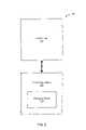
- FIG. 1illustrates a conventional pixel reset system for an active pixel.
- the illustrated pixel reset systemincludes a conventional pixel circuit and a conventional uncorrelated double sampling (UDS) circuit.
- a photodiode, D Pproduces a photo current, I P , proportional to the incident light intensity.
- the photo currentis integrated on a sense capacitor, C S .
- the sense capacitoris typically a parasitic reverse-biased PN junction capacitance associated with the photodiode and other parasitic capacitance.
- a sense MOS transistor, M 2operates as a source follower that buffers the voltage on the sense node, Node 1 , nondestructively to a readout column line.
- a row select MOS transistor, M 3acting as a switch, activates the source follower transistor when the particular row including the pixel is selected.
- the gate of a reset MOS transistor, M 1is brought up to a driving voltage, V DD , for example, and the voltage on the sense capacitor is reset to approximately V DD ⁇ V TH , where V TH is the threshold voltage of the reset transistor.
- the reset levelcontains an error from pixel to pixel.
- the errorhas two components: a fixed error component and a random reset noise.
- the fixed errorresults from mismatches between the threshold voltage and transistor sizes.
- the fixed erroris also referred to as fixed pattern noise (FPN).
- FPNnegatively affects the uniformity of the pixel responses in the pixel array. Correction of this non-uniformity may implement some type of calibration, for example, by multiplying or adding/subtracting the pixel's signal with a correction amount that is pixel dependent.
- Conventional technologies to cancel FPNmay be referred to as correlated double sampling, uncorrelated double sampling, or offset compensation, and are discussed in more detail below.
- the random reset noise(also referred to as reset noise) is generated during the reset process for the pixel.
- the shot noise in the reset transistor during resetis band-limited by the transconductance of the reset transistor and the sense capacitor. This produces a root-mean-square (RMS) noise at the sense node.
- RMS noiseis described by the following equation:
- This RMS noisemay be sampled on the sense capacitor when the reset process is complete.
- the sampled RMS noiseis 643 ⁇ V for a typical sense capacitor value of 5 fF at room temperature.
- both the fixed and random error componentscan be removed by correlated double sampling (CDS).
- CDS technologyuses two voltage measurements to remove the noise components.
- a first voltage(the reset value) is the pixel voltage immediately following a reset period. This measurement includes both the fixed and random components of the reset level error.
- the reset valuemay be stored in either analog or digital form.
- the second voltage(the integration value) is the pixel voltage after the integration period.
- the integration valuecontains the same error components introduced upon reset because the pixel has not been reset again. Additionally, the integration value includes the change in voltage on the sense capacitor due to the integrated photo current.
- a CDS circuit(not shown) outside the pixel circuit subtracts the reset value from the integration value, leaving only the light response term—the photo response voltage, V P . Thus, a CDS circuit removes both the FPN and the random reset noise.
- the photo response voltagewhich is the difference between the integration value and the reset value, is described by the following equation:
- V pI p ⁇ ⁇ T INT C S , where I P is the integrated current on the sense capacitor, T INT is the integration period during which the photo current is integrated on the sense capacitor, and C S is the capacitance of the sense capacitor.
- One drawback of conventional CDS technologyis that the reset value is stored for the duration of the integration period, which can approach the frame period.
- a storage circuit(not shown) holds the value for this entire period. For a typical imager that operates at 30 frames per second, the storage period is 33 ms.
- Analog sample-and-hold circuitsuse large and expensive hold capacitors to achieve such a long hold time.
- the storage circuitstores the reset values for the entire array of pixels because each pixel value is used for the resulting image.
- a frame buffercould be used to store the reset values for all the pixels, analog and digital frame buffers are impractical. Analog frame buffers consume significant chip area and draw substantial electrical power. For this reason, most frame buffers are digital. Digital frame buffers, however, also consume significant chip area and are expensive.
- a pinned diode pixelworks much the same way as a charge-coupled device (CCD) pixel.
- CCDcharge-coupled device
- the pixels based on pinned diodesuse additional semiconductor processing steps and also reduce the fill factor of the pixel.
- UDSuncorrelated double sampling
- FIG. 1A conventional UDS circuit uses the pixel voltage of the reset period subsequent to the current integration period, rather than the reset period prior to the integration period. In other words, the UDS circuit subtracts the subsequent reset value from the current integration value. Since the reset for a subsequent frame occurs immediately after the integration measurement of the current frame, the timeframe for storing the integration and reset values is relatively short. Typically, these measurements are held in capacitors such as in a switched-capacitor subtractor.
- the conventional UDS circuit shown in FIG. 1includes an integration sampling circuit with an input switch, S 1 , a holding capacitor, C 1 , and an output switch, S O1 .
- the integration sampling circuitsamples and holds the integration value, V O1 .
- the depicted UDS circuitalso includes a reset circuit with an input switch, S 2 , a holding capacitor, C 2 , and an output switch, S O2 .
- the reset circuitsamples and holds the reset value, V O2 . After sampling both integration value and the reset value, the output switches close and send the integration and reset values to a subtraction module (not shown) that subtracts the reset value from the integration value.
- UDS technologyremoves the fixed error (FPN) due to the threshold voltage and transistor size mismatches, it does not reduce the random reset noise because the reset noise introduced during the subsequent reset (i.e., for the next frame) is not correlated with the reset noise of the current frame.
- FPNfixed error
- UDS technologyactually increases total RMS reset noise by a factor of the square root of two because two uncorrelated noise quantities are present after the subtraction.
- UDS technologyincreases the sampled RMS noise from 643 ⁇ V to 910 ⁇ V for a typical sense capacitor value of 5 fF at room temperature. Therefore, conventional UDS technology is unsatisfactory to reduce the reset noise.
- FIG. 1illustrates a conventional pixel reset system.
- FIG. 2illustrates a schematic block diagram of one embodiment of a pixel reset system.
- FIG. 3illustrates one embodiment of an exemplary averaging module.
- FIG. 4illustrates one embodiment of a low noise reset timing diagram.
- FIG. 5illustrates another embodiment of an exemplary pixel reset system.
- FIG. 6illustrates one embodiment of a sampling method.
- FIG. 7illustrates one embodiment of an averaging method.
- FIG. 8illustrates one embodiment of an active pixel image sensor.
- FIG. 9illustrates another embodiment of an active pixel image sensor.
- FIG. 10illustrates one embodiment of an imaging system.
- circuitswhich will be described below.
- the operations of the circuitsmay be performed by a combination of hardware, firmware, and software.
- the term “coupled to,” as used herein,may mean coupled directly or indirectly through one or more intervening components. Any of the signals provided over various buses described herein may be time multiplexed with other signals and provided over one or more common buses. Additionally, the interconnection between circuit components or blocks may be shown as buses or as single signal lines. Each of the buses may alternatively be one or more single signal lines and each of the single signal lines may alternatively be buses.
- a method and apparatusare described to perform low noise reset of a pixel circuit within an active pixel image sensor.
- FIG. 2illustrates a schematic block diagram of one embodiment of a pixel reset system 100 .
- the illustrated pixel reset system 100includes a pixel circuit 110 and an averaging module 120 .
- the pixel circuit 110is coupled to a variety of sensor components 125 , including the averaging module 120 .
- the pixel circuit 110may be similar to the conventional pixel circuit shown in FIG. 1 .
- the pixel circuit 110may be different from the conventional pixel circuit. Examples of the sensor components 125 are shown and described in more detail with reference to FIGS. 8 and 9 .
- One exemplary sequence of operation of the pixel circuit 110is as follows: reset, integration, readout, reset, etc.
- the pixel circuit 110establishes a known, baseline voltage.
- the pixel circuit 110establishes a voltage relative to the light incident on the pixel circuit 110 .
- the pixel circuit 110transfers the integration voltage (or a voltage from which the integration voltage may be derived) to the averaging module 120 for processing.
- the pixel circuit 110may restart the reset period and, in one embodiment, transfers one or more reset voltages to the averaging module 120 .
- the integration and reset voltagesalso may be referred to as integration and reset values, respectively.
- the pixel circuit 110transfers the integration and reset values to the averaging module 120 via one or more of the sensor components 125 .
- the averaging module 120processes the integration value, as well as any reset values, to derive a photo response voltage, V P .
- the averaging module 120processes the integration and reset values to generate precursor values from which the photo response voltage may be derived.
- the photo response voltageis also referred to as a photo response value.
- the photo response valuecorrelates with the voltage produced on a sense node in the pixel circuit 110 in response to the light incident on the pixel circuit 110 .
- V PV INT ⁇ V (RST+1)
- V INTthe integration voltage of the pixel circuit 110 at the end of the integration period
- V (RST+1)the reset voltage (or modified reset voltage) of the averaging module 120 corresponding to the reset period immediately following the integration period.
- the averaging module 120reduces or eliminates the fixed error and/or the random reset noise due to the pixel reset, as described below. Examples of the averaging module 120 are shown and described in more detail with reference to FIGS. 3 and 5 .
- FIG. 3illustrates one embodiment of an exemplary averaging module 130 .
- the depicted averaging module 130is coupled to a readout column 135 that, in turn, is coupled to a pixel circuit (not shown) such as the pixel circuit 110 of FIG. 2 .
- the averaging module 130receives one or more independent input signals via the readout column 135 and produces two output signals, which are described in more detail below.
- the illustrated averaging module 130includes an integration circuit 140 and a reset circuit 145 .
- the integration circuit 140is configured to sample and hold the integration value.
- the integration circuit 140includes an input 150 , an input switch S 1 , a capacitor C 1 , an output switch S O1 , and an output 155 .
- the input switchcloses and the integration value integrates on the capacitor, which is coupled between the two switches and a reference voltage such as ground. In this way, the integration circuit 140 samples and holds the integration value.
- the output switchsubsequently outputs the sampled integration value, V O1 , from the integration circuit 140 .
- the reset circuit 145is similarly configured to sample and hold one or more reset values.
- the reset circuit 145may include a plurality of sampling circuits 160 .
- the depicted reset circuit 145includes three sampling circuits 160 , although other embodiments of the reset circuit 145 may include fewer or more sampling circuits 160 .
- Each sampling circuit 160includes an input 165 , an input switch S n , a capacitor C n , an output switch S On , and an output 170 .
- the input switchcloses and a reset value integrates on the capacitor, which is coupled between the two switches and a reference voltage such as ground. In this way, the sampling circuit 160 samples and holds a reset value.
- the output switchsubsequently outputs the sampled reset value from the sampling circuit 160 .
- the reset circuit 145can sample multiple reset values during a single reset period. For example, the reset circuit 145 may sequentially sample a first reset value on the capacitor C 2 , a second reset value on the capacitor C 3 , and so forth. Alternatively, the reset circuit 145 may sample some or all of the reset values in parallel. After sampling multiple reset values, the reset circuit 145 outputs the sampled reset values at approximately the same time to a common reset circuit output 175 . In one embodiment, for example, the output switch of each of the sampling circuits 160 may be coupled to a common column line. In this way, the reset circuit 145 outputs a modified reset value, V O2 , which derives from the combination of the several sampled reset values.
- V O2modified reset value
- the resulting modified reset valueis approximately the average of the sampled reset values stored in the sampling circuits 160 .
- the RMS reset noise in the reset valueis reduced by a factor of ⁇ square root over (n) ⁇ , where n is the total number or sampling circuits 160 .
- the RMS reset noise in the reset valueis reduced by approximately ⁇ square root over (3) ⁇ for a reset circuit 145 having three sampling circuits 160 .
- the reset noise in the modified reset valuecan be made arbitrarily low.
- the reset noise in the integration valueis not necessarily affected because no “averaging” occurs in the integration circuit 140 .
- the reduced noise of the modified reset valuelowers the total reset noise by up to a factor of about ⁇ square root over (2) ⁇ compared to a conventional active pixel image sensor using convention UDS technology.
- the averaging module 130is coupled to a subtraction module 180 and supplies the integration value and the modified reset value to the subtraction module 180 for further processing.
- the subtraction module 180subtracts the modified reset value from the integration value to produce a differential output voltage, V O , which may represent the photo response voltage.
- the subtraction module 180includes an operational amplifier, A, and one or more feedback capacitors, C f .
- the feedback capacitorsmay be discharged prior to receiving the integration value and the modified reset value from the averaging module 130 . Subsequently, the integration value and the modified reset value are transferred from the averaging module 130 to the subtraction module 180 to derive the differential output voltage. Additionally, the subtraction module 180 may amplify the differential output voltage. For example, the subtraction module 180 may have a gain given by the following equation:
- GC 1 C f , where C 1 is the capacitance of the integration circuit 140 and C f is the feedback capacitance of the subtraction module 180 .
- the capacitance values of the sampling circuits 160may be correlated with the capacitance of the integration circuit 140 .
- the total capacitance of all of the capacitors in the sampling circuits 160may be approximately equal to the capacitance in the integration circuit 140 .
- all of the capacitors of the sampling circuits 160may be approximately equal in size.
- the size of each of three sampling capacitancesmay be approximately 330 fF for an integration capacitance of 1 pF.
- Using smaller capacitances for the sampling circuits 160allows the size of the averaging module 130 to be approximately the same surface area on chip as a conventional UDS circuit that uses the same size capacitors (e.g., 1 pF) for both integration and reset circuitry.
- the sampling capacitorsmay be of unequal sizes and/or may have a total capacitance that is more or less than the integration capacitance.
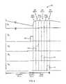
- FIG. 4illustrates one embodiment of a low noise reset timing diagram 200 .
- the depicted timing diagram 200illustrates several clocking signals for the integration and sampling circuits 140 , 160 over the integration, readout, and reset periods (identified along the horizontal axis).
- the sense voltage, V 1represents the voltage on the sense node of the pixel circuit 110 .
- the first signal 205corresponds to the activation of the input switch, S 1 , of the integration circuit 140 .
- the second signal 210corresponds to the activation of the input switch, S 2 , of a first sampling circuit 160 .
- the third signal 215corresponds to the activation of the input switch, S 3 , of a second sampling circuit 160 .
- the fourth signal 220corresponds to the activation of the input switch, S 4 , of a third sampling circuit 160 .
- the reset circuit 145may have fewer or more sampling circuits 160 and corresponding control signals.
- the integration circuit 140samples the integration value from the sense node of the pixel circuit 110 to the integration capacitor at the end of the integration period. Alternatively, the integration circuit 140 may sample and hold the integration value during the readout period.
- the pixel 110is then hard reset and soft reset. In general, a hard reset erases image lag, but introduces more noise than a soft reset. Combining a soft reset with a hard reset reduces the noise from the hard reset. However, in other embodiments, the pixel reset system 100 may use hard resets only, soft resets only, or another combination of hard and soft resets.
- the first sampling circuit 160samples the reset value of the pixel circuit 110 .
- the pixel 110is then hard reset and soft reset, again.
- the second sampling circuit 160samples the reset value of the pixel circuit 110 .
- the pixel 110is then hard reset and soft reset, again.
- the third sampling circuit 160samples the reset value of the pixel circuit 110 . This sequence may continue for as many sampling circuits 160 as are in the reset circuit 145 . Subsequently, the reset circuit 145 may generate the modified reset value and the averaging module 130 and subtraction module 180 may process the modified reset value, as described above.
- FIG. 5illustrates another embodiment of an exemplary pixel reset system 250 .
- the depicted pixel reset system 250includes a pixel circuit 255 coupled to a pixel averaging module 260 via a readout column 135 .
- the pixel circuit 255may be similar to the conventional pixel circuit of FIG. 1 , other embodiments of the pixel circuit 255 may be different from the conventional pixel circuit.
- the averaging module 260includes a first sample and hold circuit 265 , SH 1 , and a second sample and hold circuit 270 , SH 2 .
- the first SH circuit 265samples and holds the integration value.
- the second SH circuit 270samples and holds the reset value.
- the second SH circuit 270has a bandwidth that is substantially lower than the reset noise bandwidth of the pixel circuit 255 .
- the reset noise bandwidth of the pixel circuit 255is associated with the sense capacitor, C S , and the reset transistor, M 1 .
- the relatively low bandwidth of the second SH circuit 270effectively filters the reset noise from the reset value to produce a modified reset value at the output of the second SH circuit 270 .
- the modified reset valuecan be subtracted from the integration value to obtain the photo response value, as described above.
- the integration value and the modified reset valuemay be multiplexed into an ADC for processing such as subtracting the modified reset value from the integration value. Multiplexing may occur at an array level, at a column level (so the array is wholly column parallel), at a level for a subset of columns (e.g., a block of five columns), and so forth.
- the point at which certain signals may be digitized and how those signals may be multiplexed to one or more data processing devicesis not fixed and may vary depending on the implementation of the pixel circuit 110 or the pixel array or the image sensor.
- One example of an image sensor that implements multiplexing and digitizationis shown and described in more detail with reference to FIG. 9 .
- the second SH circuit 270includes analog components similar to the sampling circuit 160 of FIG. 3 .
- the resistance of the input switchmay be large, such as 100 k ⁇ or higher.
- the second SH circuit 270may include a low pass filter to cut off noise above a given bandwidth.
- Other embodiments of the second SH circuit 270may include other components to provide a relatively low bandwidth.
- N HARD1 2 ⁇ ⁇ ⁇ ⁇ ⁇ R ON ⁇ ⁇ C S , where R ON is the ON resistance of the reset transistor and C S is the capacitance of the sense capacitor of the pixel circuit 255 .
- the sampling bandwidth of the second SH circuit 270may be significantly lower than the reset noise bandwidth of a hard reset in order filter out most or all of the reset noise.
- the sampling bandwidth of the second SH circuit 270may be approximately one tenth of the reset noise bandwidth.
- N SOFTg M ⁇ ⁇ 1 2 ⁇ ⁇ ⁇ ⁇ ⁇ C S , where g M1 is the transconductance of the reset transistor of the pixel circuit 255 .
- the soft reset periodmay be very short, such as on the order of a microsecond or less, where the noise bandwidth is larger than the sampling bandwidth.
- FIG. 6illustrates one embodiment of a sampling method 300 .
- the sampling method 300may be implemented, for example, in conjunction with the averaging module 130 of FIG. 3 or another similar averaging module 120 . Additionally, the sampling method 300 may be facilitated by the processor 92 , the sequencer 96 , or other components within the image sensor 62 shown and described in FIG. 8 .
- the illustrated sampling method 300begins and the integration circuit 140 samples 305 and holds the integration voltage from the pixel circuit 110 .
- the pixel circuit 110is then hard reset and soft reset.
- a reset supply 375performs 310 the hard and soft resets.
- One example of the reset supply 375is shown in FIG. 8 .
- the reset supply 375may perform the hard reset, for example, by lowering a reset voltage supplied to the reset transistor of the pixel circuit 110 from V DD to a voltage slightly below V DD .
- the reset supply 375may perform the soft reset, for example, by raising the reset voltage back up to V DD .
- the first sampling circuit 160samples 315 and holds a first reset value.
- the first sampling circuit 160may sample the reset value after the first soft reset.
- the reset supply 375performs 320 additional hard and soft resets, similar to the first hard and soft resets.
- the second sampling circuit 160samples 325 and holds the second reset value.
- the sampling method 300continues in this cycle of resetting the pixel circuit 110 and sampling the reset values until all of the sampling circuits 160 are holding a sampled reset value.
- the sampling method 300then ends.
- the sampling method 300may discontinue after some, but before all, of the sampling circuits 160 hold sampled reset values.
- FIG. 7illustrates one embodiment of an averaging method 350 .
- the averaging method 350may be implemented, for example, in conjunction with the averaging module 130 of FIG. 3 , the averaging module 260 of FIG. 5 , or another similar averaging module 120 . Additionally, the averaging method 350 may be facilitated by the processor 92 , the sequencer 96 , or other components within the image sensor 62 shown and described in FIG. 8 .
- the illustrated averaging method 350begins and the integration circuit 140 outputs 355 the integration value to the subtraction module 180 . Simultaneously, or at approximately the same time, the sampling circuits 160 output 360 the plurality of sampled reset values to the common reset circuit output 175 . As explained above, outputting the sampled reset values to the common reset output 175 redistributes the sampled reset values so that the reset circuit 145 outputs 365 a modified reset value.
- the modified reset valueis an “average” of the various sampled reset values.
- the reset circuit 145may output a modified reset value that is not based on multiple sampled reset values.
- the subtraction module 180subsequently takes the integration value and the modified reset value as inputs to generate a differential value. In one embodiment, the differential value is the integration value minus the modified reset value.
- the depicted averaging method 350then ends.
- averaging module 120may include an analog-to-digital converter (ADC) to perform some or all of the averaging operations in the digital domain, rather than in the analog domain.
- ADCanalog-to-digital converter
- a digital averaging module 390may use a plurality of digitized reset values to generate a digital modified reset value. Then the digital averaging module 390 may digitally subtract the digital modified reset value from a digital integration value to produce the digital differential output value.
- ADCanalog-to-digital converter
- the digital averaging module 390may include a tracking ADC and calculate a digital modified reset valued from a plurality of digital sampled reset values.
- the digital modified reset valuemay be a digital “average” of the plurality of digital sampled reset values.
- the digital averaging module 390may produce the digital differential output value in a manner similar to the process described above.
- One example of an image sensor configured to perform such digital averagingis shown described in more detail with reference to FIG. 9 .
- some or all of the averaging operationsmay be performed by software rather than hardware.
- the softwaremay be executed on a digital processing device.
- the term “module”is used herein to encompass hardware, including analog and/or digital hardware components, and software implementations.
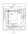
- FIG. 8illustrates one embodiment of an active pixel image sensor 62 .
- the active pixel image sensor 62is also shown and described in the context of an imaging system in FIG. 10 .
- the image sensor 62is a color complimentary metal-oxide semiconductor (CMOS) image sensor.
- CMOScomplementary metal-oxide semiconductor
- MOSmetal-oxide semiconductor
- the illustrated image sensor 62includes an imaging core 64 that includes a pixel matrix 66 and electronic components (imaging electronics) associated with the operation of the imaging core 64 .
- the imaging core 64includes a pixel matrix 66 having an array of pixel circuits 110 (also referred to as pixels 110 ) and the corresponding driving and sensing circuitry for each pixel 110 .
- the pixel matrix 66may be arranged in M columns of pixels 110 by N rows of pixels 110 . Although detailed embodiments of the pixels 110 are described above with reference to previous figures, each pixel 110 has a width and a length and includes at least a photosensitive element and a readout switch. In certain embodiments, the pixels 110 of the pixel matrix 66 may be linear response pixels 110 (i.e., having linear or piecewise linear slopes).
- Each row of pixels 110is coupled to a reset line 70 and a row select line 72 (also referred to as a select line).
- the reset line 70is coupled to a reset supply 375 .
- the row select line 72is coupled to a row select supply 380 .
- each column of pixels 110is coupled to a source column 385 and a readout column 135 (also referred to as a readout line). Examples of the readout column 135 are shown and described in more detail with reference to FIGS. 3 and 5 .
- the readout column 135may be coupled to an averaging module 120 , although other embodiments of the image sensor 62 may omit the averaging module 120 .
- each pixel 110 within a rowmay be coupled to other circuitry that couples one or more pixels 110 , rows, or columns.
- the pixel array 66may have approximately 2,000 columns by 1,500 rows of pixels 110 .
- Each pixel 110may be an adaptive dynamic range photodiode that is, for example, approximately 3.35 ⁇ m by 3.35 ⁇ m in size.
- the resulting pixel array 66 for that size of pixel 110is about 6.75 mm by 5.08 mm in size.
- the pixel array 66may have more or less pixels 110 , rows, or columns, or include other types and/or sizes of pixels 110 .
- the driving and sensing circuitry of the imaging core 64may include one or more Y-addressing scanning registers 74 and one or more X-addressing scanning registers 76 in the form of shift registers or addressing registers.
- the circuitry of the imaging core 64also may include buffers and/or line drivers (not shown) for the long reset and select lines.
- the circuitry of the imaging core 64also includes a subtraction module 180 , as described above with reference to FIG. 3 .
- the CDS circuitryis on-chip. In another embodiment, the subtraction module 180 is on a separate chip.
- the circuitry of the imaging core 64also may include an analog multiplexer 80 coupled to an output bus 82 .
- the Y-addressing scan register 74addresses via the row select line 72 all of the pixels 110 of a row of the pixel matrix 66 to be read out. In this way, all of the switching elements of the pixels 110 of the selected row may be closed at approximately the same time to place a signal on a corresponding number of readout columns 135 .
- the individual signalsare subsequently processed and/or amplified in the subtraction module 180 . Additionally, one or more filters may be used to improve the integrity of the signal.
- the X-addressing scan register 76provides control signals to the analog multiplexer 80 to place an output signal (e.g., amplified charges) of the subtraction module 180 onto the output bus 82 .
- the output bus 82may be coupled to an output buffer 84 that provides an analog output 86 from the imaging core 64 .
- additional amplifiers and/or filtersmay enhance the output signal 86 after it has been transmitted from the analog multiplexer 80 .
- the output signal 86 from the imaging core 64is coupled to an analog-to-digital converter (ADC) 90 to convert the analog imaging core output 86 into the digital domain.
- ADC 90is an on-chip 12-bit column parallel ADC.
- the ADC 90is coupled to a digital processing device 92 to process the digital data received from the ADC 90 . Such processing may be referred to as imaging processing or post-processing.
- the digital processing device 92may include one or more general-purpose processing devices such as a microprocessor or central processing unit, a controller, or the like. Alternatively, the digital processing device 92 may include one or more special-purpose processing devices such as a digital signal processor (DSP), an application specific integrated circuit (ASIC), a field programmable gate array (FPGA), or the like. In an alternative embodiment, for example, the digital processing device 92 may be a network processor having multiple processors including a core unit and multiple microengines. Additionally, the digital processing device 92 may include any combination of general-purpose processing device(s) and special-purpose processing device(s).
- DSPdigital signal processor
- ASICapplication specific integrated circuit
- FPGAfield programmable gate array
- the digital processing device 92is coupled to an interface module 94 that handles the input/output (I/O) exchange with other components of the imaging system 10 .
- the interface module 94also may manage other tasks such as protocols, handshaking, voltage conversions, and so forth.
- the interface module 94is coupled to a sequencer 96 .
- the sequencer 96may be coupled to one or more components in the image sensor 62 such as, for example, the imaging core 64 , the digital processing device 92 , and the ADC 90 .
- the sequencer 96may be a digital circuit that receives externally generated clock and control signals via the interface module 94 and generates internal pulses to drive circuitry (for example, the imaging core 64 , the ADC 90 , etc.) in the imaging sensor 62 .
- FIG. 9illustrates another embodiment of an image sensor 98 .
- the illustrated image sensor 98includes many of the same components as the image sensor 62 of FIG. 8 .
- like componentsare identified by the same reference numbers and operate in a similar or identical manner as described above with reference to FIG. 8 , except for any differences described below.
- the depicted image sensor 98 of FIG. 9includes a digital averaging module 390 and a sampling circuit 395 .
- the digital averaging module 390may include an ADC or a tracking ADC.
- the digital averaging module 390may be coupled to a separate ADC within the image sensor 98 .
- the digital averaging module 390facilitates converting analog sample signals into corresponding signals.
- the digital averaging module 390may perform some or all of the processing of the digitized integration and reset values in order to produce a digital photo response value.
- the sampling circuit 395is substantially similar to the sampling circuit 160 of FIG. 3 or the SH circuits 265 , 270 of FIG. 5 .
- the sampling circuit 395includes one or more circuits to sample one or more readout lines 135 from the pixel array 66 .
- the sampling circuit 395also may include amplification and/or buffer circuitry.
- image sensor 62 of FIG. 8 and the image sensor 98 of FIG. 9may differ from the depicted embodiments in size, components, layout, and so forth.
- alternative embodiments of the image sensors 62 , 98may include one ADC 90 for every pixel 110 , for every column, or for a subset block of columns.
- one or more other components within the image sensors 62 , 98may be duplicated and/or reconfigured for parallel or enhanced performance.
- layout of the individual components within the image sensors 62 , 98may be modified to adapt to the number and type of components.
- some of the operations performed by the image sensors 62 , 98may be performed in the digital domain instead of the analog domain, and vice versa.
- these alternative embodimentsare all within the scope of this description.
- the pixel matrix 66 and associated imaging electronics within the imaging core 64may each reside on a different die substrate and in different chip packages.
- the electronic components within the imaging core 64may reside in a common chip package on separate integrated circuit die substrates or on a common die substrate.
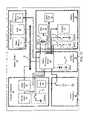
- FIG. 10illustrates one embodiment of an imaging system 10 .
- the imaging system 10is representative of various imaging systems that may be incorporated in one or more types of imaging devices, including still cameras, video cameras, scanners, automotive cameras, and so forth.
- the imaging system 10may be referred to as a camera 10 , but is nevertheless understood to be representative of other types of imaging systems.
- the illustrated imaging system 10includes a control subsystem 20 , a power subsystem 22 , an imaging subsystem 24 , a storage subsystem 26 , and an interface subsystem 28 . Although each of these subsystems is described herein with particular detail, other embodiments of the imaging system 10 may include fewer or more subsystems and/or fewer or more component parts of the individual subsystems.
- the control subsystem 20includes a digital processing device 30 .
- the digital processing device 30may be may include one or more general-purpose processing devices such as a microprocessor or central processing unit, a controller, or the like.
- the digital processing device 30may include one or more special-purpose processing devices such as a digital signal processor (DSP), an application specific integrated circuit (ASIC), a field programmable gate array (FPGA), or the like.
- the digital processing device 30may include any combination of general-purpose processing device(s) and special-purpose processing device(s).
- the digital processing device 30may be a network processor having multiple processors including a core unit and multiple microengines.
- the digital processing device 30is an ASIC, but references to the ASIC 30 herein are understood to be representative of the digital processing device 30 , generally.
- the digital processing device 30may include a microprocessor, one or more memory devices, control logic, and the like, in order to implement particular operations within imaging system 10 .
- the digital processing device 30may facilitate taking a digital picture, including acquiring an image via the imaging subsystem 24 , digitizing the image, processing the image, displaying the image via the interface subsystem 28 , storing the image via the storage subsystem 26 , and transferring the image to an external storage device (not shown).
- the digital processing device 30may implement instructions from a user received via the interface subsystem 28 .
- the digital processing device 30also may include an internal read-only memory (ROM) for firmware storage.
- the digital processing device 30may facilitate firmware or software updates within the imaging system 10 .
- the control subsystem 20also may include a quartz crystal 32 , oscillator, or other clocking device to supply a clock signal to the digital processing device 30 .
- the power subsystem 22includes a battery circuit to supply electrical power to the digital processing device 30 and other subsystems within the imaging system 10 .
- the power subsystem 22may include a permanent battery, temporary batteries, a recharging circuit, regulators or other current control circuitry, one or more switches, and so forth.
- the power subsystem 22may include a power adapter to accept alternating current (AC) or direct current (DC) power from an external power supply (not shown).
- the power subsystem 22may be configured to accept power via a universal serial bus (USB) port, or other communication port, whenever the imaging system 10 is plugged into a PC or other computing device.
- USBuniversal serial bus
- the imaging subsystem 24includes a lens assembly 34 having one or more optical lenses, a shutter 36 , a strobe flash 38 , and the image sensor 62 .
- the imaging subsystem 24captures images and converts them into digital form.
- the image sensor 62may be coupled to a bus 42 that is coupled to the digital processing device 30 .
- One example of the image sensor 62is depicted and described in more detail with reference to FIG. 4 .
- the lens assembly 34directs incident light to a pixel array within the image sensor 62 .
- the lens assembly 34may include a lens stack integrated with the image sensor 62 .
- the lens assembly 34may have other characteristics.
- the shutter 36allows the light to be detected by the image sensor 62 .
- the strobe flash 38provides additional light, in addition to any ambient light, to illuminate a scene approximately during the time the image sensor 62 detects an image. In one example, the strobe flash 38 automatically activates in response to detected low light levels.
- lens assemblies, shutters, and flashesthat are generally known in the art may be suitable for use with the imaging system 10 , although more specialized or custom devices also may be used with the imaging system 10 .
- the storage subsystem 26includes a flash memory device 44 , a random access memory (RAM) device 46 , and a memory card 48 .
- a flash memory 44is depicted, other types of memory may be used in conjunction with or in place of the flash memory 44 , including read-only memory (ROM), programmable ROM (PROM), erasable PROM (EPROM), and electrically erasable PROM (EEPROM).
- ROMread-only memory
- PROMprogrammable ROM
- EPROMerasable PROM
- EEPROMelectrically erasable PROM
- the flash memory 44 and the RAM 46may be coupled to the bus 42 .
- the digital processing device 30may coordinate bus arbitration and the transfer of image data from the imaging subsystem 24 to the storage subsystem 26 .
- the RAM 46may be nonvolatile and store software or other control instructions that are used by the digital processing device 30 to operate the imaging system 10 .
- the digital processing device 30may load firmware instructions from an internal ROM into the RAM 46 .
- the RAM 46is synchronous RAM (SRAM).
- the RAM 46is synchronous dynamic RAM (SDRAM).
- SDRAMsynchronous dynamic RAM
- the RAM 46may be another type of volatile or nonvolatile RAM.
- the flash memory 44 or the RAM 46may store images and/or image metadata (e.g., image capture parameters, camera mode settings, electrical power settings, etc.) from the imaging subsystem 24 , for example.
- the image datais initially stored in the RAM 46 and then transferred to the flash memory 44 for more permanent storage.
- the digital processing device 30may initiate a direct memory transfer (DMA) to transfer the image data from the RAM 46 to the flash memory 44 .
- the microprocessor within the digital processing device 30may include several DMA engines to perform the DMA operations. In certain embodiments, the DMA engines may facilitate the following transfers: imaging subsystem 24 to RAM 46 , RAM 46 to flash memory 44 , flash memory to RAM 46 , RAM 46 to memory card 48 , memory card 48 to RAM 46 , and so forth.
- the flash memory 44is NAND flash memory ranging in size from 4 to 32 megabytes (MB), although other types and/or sizes of flash memory may be used.
- the memory card 48is a memory card such as a secure digital (SD) memory card, a mini SD card, an ultra-compact (xD) memory card, a multimedia card (MMC), a microdrive, a universal serial bus (USB) flash drive, or another type of removable or non-removable memory media.
- the memory card 48may be permanently coupled to the storage subsystem 26 .
- the interface subsystem 28includes a user interface (I/F) module 50 , a display device 52 , one or more sound modules 54 , one or more mode modules 56 , a piezo buzzer module 58 (also known as a piezo resonator), and a communication port 60 .
- the user interface module 50may include hardware components such as buttons, as well as accompanying software, to allow a user to interface with the imaging system 10 .
- the user interface module 50may allow a user to make selections regarding the operation of the imaging system 10 , the use of the strobe flash 38 and other capture parameters, the location of stored images on the storage subsystem 26 , and so forth.
- the interface subsystem 28may be partially or wholly configurable by the firmware.
- the display device 52communicates visual images, including digitized images from the imaging subsystem 24 , user selection menus, status indicators, and so forth, to the user.
- the display device 52is a liquid crystal display (LCD) such as a thin film transistor (TFT) display.
- the display device 52may employ another technology to generate and present an image to the user.
- the sound module 54controls sounds produced by the imaging system 10 .
- the mode module 56controls the operational mode of the imaging system 10 .
- the imaging system 10may have various capture modes, including bright, dark, far, near, action, portrait, and so forth.
- the buzzer module 58in one embodiment, is a piezo resonator to produce variable pitch tones.
- the communication port 60allows connectivity with another electronic device such as a desktop computer (not shown) or other computing device.
- the communication port 60is a USB port, but references to the USB port 60 herein are understood to refer to the communication port 60 , generally.
- the communication port 60may be used to provide power to recharge a battery in the power subsystem 22 , transfer images and image metadata from the storage subsystem 26 (e.g., the flash memory 44 or the memory card 48 ) to a desktop computer, for example, and communicate firmware upgrades from the desktop, for example, to the digital processing device 30 .
- the communication port 60may be a USB 2.0 port.
- the electronic components of the imaging system 10may each reside on a different die substrate and in different chip packages. Alternatively, some or all of the electronic components of the imaging system 10 may reside in a common chip package on separate integrated circuit die substrates or on a common die substrate.
- the image sensor 62 discussed hereinmay be used in various applications.
- embodiments of the image sensor 62may be used in a digital camera system for general-purpose photography (e.g., camera phone, still camera, video camera) or special-purpose photography.
- the image sensor 62may be used in other types of applications.
- embodiments of the image sensor 62may be used in machine vision, document scanning, microscopy, security, biometry, and other similar applications.
Landscapes
- Engineering & Computer Science (AREA)
- Multimedia (AREA)
- Signal Processing (AREA)
- Transforming Light Signals Into Electric Signals (AREA)
Abstract
Description
where CSis the capacitance of the sense capacitor, T is the absolute temperature (Kelvin) of the reset transistor, and k is Boltzmann's constant. This RMS noise may be sampled on the sense capacitor when the reset process is complete. As an example, the sampled RMS noise is 643 μV for a typical sense capacitor value of 5 fF at room temperature.
where IPis the integrated current on the sense capacitor, TINTis the integration period during which the photo current is integrated on the sense capacitor, and CSis the capacitance of the sense capacitor.
VP=VINT−V(RST+1),
where VINTis the integration voltage of the
where C1is the capacitance of the
where RONis the ON resistance of the reset transistor and CSis the capacitance of the sense capacitor of the
where gM1is the transconductance of the reset transistor of the
Claims (34)
Priority Applications (1)
| Application Number | Priority Date | Filing Date | Title |
|---|---|---|---|
| US11/250,114US7609303B1 (en) | 2004-10-12 | 2005-10-12 | Low noise active pixel image sensor using a modified reset value |
Applications Claiming Priority (2)
| Application Number | Priority Date | Filing Date | Title |
|---|---|---|---|
| US61790004P | 2004-10-12 | 2004-10-12 | |
| US11/250,114US7609303B1 (en) | 2004-10-12 | 2005-10-12 | Low noise active pixel image sensor using a modified reset value |
Publications (1)
| Publication Number | Publication Date |
|---|---|
| US7609303B1true US7609303B1 (en) | 2009-10-27 |
Family
ID=41211103
Family Applications (1)
| Application Number | Title | Priority Date | Filing Date |
|---|---|---|---|
| US11/250,114Expired - Fee RelatedUS7609303B1 (en) | 2004-10-12 | 2005-10-12 | Low noise active pixel image sensor using a modified reset value |
Country Status (1)
| Country | Link |
|---|---|
| US (1) | US7609303B1 (en) |
Cited By (58)
| Publication number | Priority date | Publication date | Assignee | Title |
|---|---|---|---|---|
| US20070139729A1 (en)* | 2005-12-16 | 2007-06-21 | Gi-Doo Lee | Image sensor and test system and method therefor |
| US20110148523A1 (en)* | 2009-12-23 | 2011-06-23 | Omnivision Technologies, Inc. | Op-amp sharing with input and output reset |
| US20110217697A1 (en)* | 2008-06-25 | 2011-09-08 | Life Technologies Corporation | Methods and apparatus for measuring analytes using large scale fet arrays |
| US20110276746A1 (en)* | 2010-05-05 | 2011-11-10 | Arvind Pruthi | Caching storage adapter architecture |
| WO2012039812A1 (en)* | 2010-09-24 | 2012-03-29 | Life Technologies Corporation | Matched pair transistor circuits |
| US20130082681A1 (en)* | 2011-09-29 | 2013-04-04 | E Ink Holdings Inc. | Detecting circuit |
| US8415716B2 (en) | 2006-12-14 | 2013-04-09 | Life Technologies Corporation | Chemically sensitive sensors with feedback circuits |
| US8421437B2 (en) | 2010-06-30 | 2013-04-16 | Life Technologies Corporation | Array column integrator |
| US8435395B2 (en) | 2006-12-14 | 2013-05-07 | Life Technologies Corporation | Methods and apparatus for measuring analytes using large scale FET arrays |
| US8459773B2 (en) | 2010-09-15 | 2013-06-11 | Electronics For Imaging, Inc. | Inkjet printer with dot alignment vision system |
| US8462240B2 (en) | 2010-09-15 | 2013-06-11 | Aptina Imaging Corporation | Imaging systems with column randomizing circuits |
| US8552771B1 (en) | 2012-05-29 | 2013-10-08 | Life Technologies Corporation | System for reducing noise in a chemical sensor array |
| US8592153B1 (en) | 2009-05-29 | 2013-11-26 | Life Technologies Corporation | Methods for manufacturing high capacitance microwell structures of chemically-sensitive sensors |
| US8747748B2 (en) | 2012-01-19 | 2014-06-10 | Life Technologies Corporation | Chemical sensor with conductive cup-shaped sensor surface |
| US8776573B2 (en) | 2009-05-29 | 2014-07-15 | Life Technologies Corporation | Methods and apparatus for measuring analytes |
| US8821798B2 (en) | 2012-01-19 | 2014-09-02 | Life Technologies Corporation | Titanium nitride as sensing layer for microwell structure |
| US8841217B1 (en) | 2013-03-13 | 2014-09-23 | Life Technologies Corporation | Chemical sensor with protruded sensor surface |
| US8858782B2 (en) | 2010-06-30 | 2014-10-14 | Life Technologies Corporation | Ion-sensing charge-accumulation circuits and methods |
| US8936763B2 (en) | 2008-10-22 | 2015-01-20 | Life Technologies Corporation | Integrated sensor arrays for biological and chemical analysis |
| US8963216B2 (en) | 2013-03-13 | 2015-02-24 | Life Technologies Corporation | Chemical sensor with sidewall spacer sensor surface |
| US8962366B2 (en) | 2013-01-28 | 2015-02-24 | Life Technologies Corporation | Self-aligned well structures for low-noise chemical sensors |
| US20150124138A1 (en)* | 2013-11-07 | 2015-05-07 | Renesas Electronics Corporation | Solid-state image sensing device |
| WO2015095613A1 (en)* | 2013-12-19 | 2015-06-25 | Kla-Tencor Corporation | A low-noise sensor and an inspection system using a low-noise sensor |
| US9080968B2 (en) | 2013-01-04 | 2015-07-14 | Life Technologies Corporation | Methods and systems for point of use removal of sacrificial material |
| US9109251B2 (en) | 2004-06-25 | 2015-08-18 | University Of Hawaii | Ultrasensitive biosensors |
| US9116117B2 (en) | 2013-03-15 | 2015-08-25 | Life Technologies Corporation | Chemical sensor with sidewall sensor surface |
| US9128044B2 (en) | 2013-03-15 | 2015-09-08 | Life Technologies Corporation | Chemical sensors with consistent sensor surface areas |
| US20160014361A1 (en)* | 2014-07-09 | 2016-01-14 | Commissariat à l'énergie atomique et aux énergies alternatives | Correlated multiple sampling cmos image sensor |
| US20160037092A1 (en)* | 2014-07-30 | 2016-02-04 | Dongbu Hitek Co., Ltd. | Image Sensor |
| US9307167B2 (en)* | 2011-10-18 | 2016-04-05 | Sony Corporation | Image pickup device and image pickup display system for reducing afterimage in image output |
| US9404920B2 (en) | 2006-12-14 | 2016-08-02 | Life Technologies Corporation | Methods and apparatus for detecting molecular interactions using FET arrays |
| US9410901B2 (en) | 2014-03-17 | 2016-08-09 | Kla-Tencor Corporation | Image sensor, an inspection system and a method of inspecting an article |
| US9618475B2 (en) | 2010-09-15 | 2017-04-11 | Life Technologies Corporation | Methods and apparatus for measuring analytes |
| US9671363B2 (en) | 2013-03-15 | 2017-06-06 | Life Technologies Corporation | Chemical sensor with consistent sensor surface areas |
| US20170195605A1 (en)* | 2015-12-31 | 2017-07-06 | James Alves | Digital camera control system |
| US9748294B2 (en) | 2014-01-10 | 2017-08-29 | Hamamatsu Photonics K.K. | Anti-reflection layer for back-illuminated sensor |
| US9823217B2 (en) | 2013-03-15 | 2017-11-21 | Life Technologies Corporation | Chemical device with thin conductive element |
| US9835585B2 (en) | 2013-03-15 | 2017-12-05 | Life Technologies Corporation | Chemical sensor with protruded sensor surface |
| US9841398B2 (en) | 2013-01-08 | 2017-12-12 | Life Technologies Corporation | Methods for manufacturing well structures for low-noise chemical sensors |
| WO2017214391A1 (en)* | 2016-06-08 | 2017-12-14 | Invisage Technologies, Inc. | Image sensors with electronic shutter |
| US9960253B2 (en) | 2010-07-03 | 2018-05-01 | Life Technologies Corporation | Chemically sensitive sensor with lightly doped drains |
| US9960783B2 (en) | 2015-09-18 | 2018-05-01 | Taiwan Semiconductor Manufacturing Company Ltd. | Conditional correlated multiple sampling single slope analog-to-digital converter, and associated image sensor system and method |
| US9970984B2 (en) | 2011-12-01 | 2018-05-15 | Life Technologies Corporation | Method and apparatus for identifying defects in a chemical sensor array |
| US10077472B2 (en) | 2014-12-18 | 2018-09-18 | Life Technologies Corporation | High data rate integrated circuit with power management |
| US10096730B2 (en) | 2016-01-15 | 2018-10-09 | Invisage Technologies, Inc. | High-performance image sensors including those providing global electronic shutter |
| US10100357B2 (en) | 2013-05-09 | 2018-10-16 | Life Technologies Corporation | Windowed sequencing |
| US10313622B2 (en) | 2016-04-06 | 2019-06-04 | Kla-Tencor Corporation | Dual-column-parallel CCD sensor and inspection systems using a sensor |
| US10379079B2 (en) | 2014-12-18 | 2019-08-13 | Life Technologies Corporation | Methods and apparatus for measuring analytes using large scale FET arrays |
| US10397504B2 (en) | 2017-02-13 | 2019-08-27 | Kidde Technologies, Inc. | Correcting lag in imaging devices |
| US10451585B2 (en) | 2009-05-29 | 2019-10-22 | Life Technologies Corporation | Methods and apparatus for measuring analytes |
| US10458942B2 (en) | 2013-06-10 | 2019-10-29 | Life Technologies Corporation | Chemical sensor array having multiple sensors per well |
| US10605767B2 (en) | 2014-12-18 | 2020-03-31 | Life Technologies Corporation | High data rate integrated circuit with transmitter configuration |
| US10778925B2 (en) | 2016-04-06 | 2020-09-15 | Kla-Tencor Corporation | Multiple column per channel CCD sensor architecture for inspection and metrology |
| US11114491B2 (en) | 2018-12-12 | 2021-09-07 | Kla Corporation | Back-illuminated sensor and a method of manufacturing a sensor |
| US11231451B2 (en) | 2010-06-30 | 2022-01-25 | Life Technologies Corporation | Methods and apparatus for testing ISFET arrays |
| US11307166B2 (en) | 2010-07-01 | 2022-04-19 | Life Technologies Corporation | Column ADC |
| US11339430B2 (en) | 2007-07-10 | 2022-05-24 | Life Technologies Corporation | Methods and apparatus for measuring analytes using large scale FET arrays |
| EP4349004A4 (en)* | 2021-05-28 | 2024-09-11 | Varex Imaging Corporation | COMBINED IMAGING ARRAY AND STRIP AND PIXEL NOISE REDUCTION SYSTEM |
Citations (20)
| Publication number | Priority date | Publication date | Assignee | Title |
|---|---|---|---|---|
| US5946033A (en)* | 1996-05-28 | 1999-08-31 | Gatan, Inc. | Method and apparatus for multiple read-out speeds for a CTD |
| US5949483A (en)* | 1994-01-28 | 1999-09-07 | California Institute Of Technology | Active pixel sensor array with multiresolution readout |
| US6115066A (en)* | 1997-06-12 | 2000-09-05 | International Business Machines Corporation | Image sensor with direct digital correlated sampling |
| US6320616B1 (en) | 1997-06-02 | 2001-11-20 | Sarnoff Corporation | CMOS image sensor with reduced fixed pattern noise |
| US20020033439A1 (en)* | 2000-05-16 | 2002-03-21 | Bock Nikolai E. | Image sensors with pixel reset |
| US20020158982A1 (en)* | 2001-04-26 | 2002-10-31 | Fujitsu Limited | X-Y address type solid-state image pickup device |
| US6493030B1 (en) | 1998-04-08 | 2002-12-10 | Pictos Technologies, Inc. | Low-noise active pixel sensor for imaging arrays with global reset |
| US6697111B1 (en) | 1998-04-08 | 2004-02-24 | Ess Technology, Inc. | Compact low-noise active pixel sensor with progressive row reset |
| WO2004064025A2 (en) | 2003-01-08 | 2004-07-29 | Smal Camera Technologies | Cmos active pixel with hard and soft reset |
| US6777660B1 (en) | 2002-02-04 | 2004-08-17 | Smal Technologies | CMOS active pixel with reset noise reduction |
| US6801255B2 (en)* | 2000-02-29 | 2004-10-05 | Canon Kabushiki Kaisha | Image pickup apparatus |
| US6903670B1 (en) | 2002-10-04 | 2005-06-07 | Smal Camera Technologies | Circuit and method for cancellation of column pattern noise in CMOS imagers |
| US6911640B1 (en)* | 2002-04-30 | 2005-06-28 | Ess Technology, Inc. | Reducing reset noise in CMOS image sensors |
| US6917027B2 (en)* | 2001-04-04 | 2005-07-12 | Micron Technology Inc. | Method and apparatus for reducing kTC noise in an active pixel sensor (APS) device |
| US20050206752A1 (en)* | 2004-03-16 | 2005-09-22 | Samsung Electronics Co., Ltd. | Method and circuit for performing correlated double sub-sampling (CDSS) of pixels in an active pixel sensor (APS) array |
| US20060077273A1 (en)* | 2004-10-12 | 2006-04-13 | Hae-Seung Lee | Low noise active pixel image sensor |
| US7045753B1 (en)* | 2000-08-09 | 2006-05-16 | Dalsa, Inc. | Five transistor CMOS pixel |
| US7154075B2 (en)* | 2003-11-13 | 2006-12-26 | Micron Technology, Inc. | Method and apparatus for pixel signal binning and interpolation in column circuits of a sensor circuit |
| US20080062286A1 (en)* | 2006-09-07 | 2008-03-13 | Jeffery Steven Beck | Method and apparatus for suppressing noise in image sensor devices |
| US7456879B2 (en)* | 2003-08-29 | 2008-11-25 | Aptina Imaging Corporation | Digital correlated double sampling using dual analog path |
- 2005
- 2005-10-12USUS11/250,114patent/US7609303B1/ennot_activeExpired - Fee Related
Patent Citations (24)
| Publication number | Priority date | Publication date | Assignee | Title |
|---|---|---|---|---|
| US5949483A (en)* | 1994-01-28 | 1999-09-07 | California Institute Of Technology | Active pixel sensor array with multiresolution readout |
| US5946033A (en)* | 1996-05-28 | 1999-08-31 | Gatan, Inc. | Method and apparatus for multiple read-out speeds for a CTD |
| US6320616B1 (en) | 1997-06-02 | 2001-11-20 | Sarnoff Corporation | CMOS image sensor with reduced fixed pattern noise |
| US6115066A (en)* | 1997-06-12 | 2000-09-05 | International Business Machines Corporation | Image sensor with direct digital correlated sampling |
| US6493030B1 (en) | 1998-04-08 | 2002-12-10 | Pictos Technologies, Inc. | Low-noise active pixel sensor for imaging arrays with global reset |
| US6697111B1 (en) | 1998-04-08 | 2004-02-24 | Ess Technology, Inc. | Compact low-noise active pixel sensor with progressive row reset |
| US6801255B2 (en)* | 2000-02-29 | 2004-10-05 | Canon Kabushiki Kaisha | Image pickup apparatus |
| US20020033439A1 (en)* | 2000-05-16 | 2002-03-21 | Bock Nikolai E. | Image sensors with pixel reset |
| US7045753B1 (en)* | 2000-08-09 | 2006-05-16 | Dalsa, Inc. | Five transistor CMOS pixel |
| US6917027B2 (en)* | 2001-04-04 | 2005-07-12 | Micron Technology Inc. | Method and apparatus for reducing kTC noise in an active pixel sensor (APS) device |
| US20020158982A1 (en)* | 2001-04-26 | 2002-10-31 | Fujitsu Limited | X-Y address type solid-state image pickup device |
| US6777660B1 (en) | 2002-02-04 | 2004-08-17 | Smal Technologies | CMOS active pixel with reset noise reduction |
| US6911640B1 (en)* | 2002-04-30 | 2005-06-28 | Ess Technology, Inc. | Reducing reset noise in CMOS image sensors |
| US6903670B1 (en) | 2002-10-04 | 2005-06-07 | Smal Camera Technologies | Circuit and method for cancellation of column pattern noise in CMOS imagers |
| US20050083422A1 (en) | 2003-01-08 | 2005-04-21 | Hae-Seung Lee | CMOS active pixel with hard and soft reset |
| US20040174450A1 (en) | 2003-01-08 | 2004-09-09 | Hae-Seung Lee | CMOS active pixel with hard and soft reset |
| US20040174449A1 (en) | 2003-01-08 | 2004-09-09 | Hae-Seung Lee | CMOS active pixel with hard and soft reset |
| WO2004064025A2 (en) | 2003-01-08 | 2004-07-29 | Smal Camera Technologies | Cmos active pixel with hard and soft reset |
| US7446805B2 (en)* | 2003-01-08 | 2008-11-04 | Cypress Semiconductor Corporation | CMOS active pixel with hard and soft reset |
| US7456879B2 (en)* | 2003-08-29 | 2008-11-25 | Aptina Imaging Corporation | Digital correlated double sampling using dual analog path |
| US7154075B2 (en)* | 2003-11-13 | 2006-12-26 | Micron Technology, Inc. | Method and apparatus for pixel signal binning and interpolation in column circuits of a sensor circuit |
| US20050206752A1 (en)* | 2004-03-16 | 2005-09-22 | Samsung Electronics Co., Ltd. | Method and circuit for performing correlated double sub-sampling (CDSS) of pixels in an active pixel sensor (APS) array |
| US20060077273A1 (en)* | 2004-10-12 | 2006-04-13 | Hae-Seung Lee | Low noise active pixel image sensor |
| US20080062286A1 (en)* | 2006-09-07 | 2008-03-13 | Jeffery Steven Beck | Method and apparatus for suppressing noise in image sensor devices |
Non-Patent Citations (5)
| Title |
|---|
| "International Search Report", International Searching Authority, PCT/US2004/000153, Jul. 29, 2004, 3 pages. |
| "Ultra-Pocket(R) 5 Kit. Rapid Development Kit for 3.0-Megapixel Credit Card Cameras with Color TFT LCD Display", SMal Camera, Aug. 25, 2005, pp. 1-3, Technologies, http:www.smalcamera.com/up51cd.html. |
| "Written Opinion of the International Searching Authority", International Searching Authority, PCT/US2004/000153, Jul. 29, 2004, 8 pages. |
| Decker et al., "A 256x256 CMOS Imaging Array with Wide Dynamic Range Pixels and Column-Parallel Digital Output", IEEE Journal of Solid-State Circuits, Dec. 1998, vol. 33, No. 12, pp. 2081-2091. |
| Kozlowski et al., "A Progressive 1920x1080 Imaging System-on-Chip for HDTV Cameras", IEEE International Solid-State Circuits Conference, Feb. 8, 2005, Session 19, Digest of Technical Papers, pp. 358-359. |
Cited By (172)
| Publication number | Priority date | Publication date | Assignee | Title |
|---|---|---|---|---|
| US10563252B2 (en) | 2004-06-25 | 2020-02-18 | University Of Hawaii | Ultrasensitive biosensors |
| US9109251B2 (en) | 2004-06-25 | 2015-08-18 | University Of Hawaii | Ultrasensitive biosensors |
| US20070139729A1 (en)* | 2005-12-16 | 2007-06-21 | Gi-Doo Lee | Image sensor and test system and method therefor |
| US9269708B2 (en) | 2006-12-14 | 2016-02-23 | Life Technologies Corporation | Methods and apparatus for measuring analytes using large scale FET arrays |
| US8496802B2 (en) | 2006-12-14 | 2013-07-30 | Life Technologies Corporation | Methods for operating chemically-sensitive sample and hold sensors |
| US9989489B2 (en) | 2006-12-14 | 2018-06-05 | Life Technnologies Corporation | Methods for calibrating an array of chemically-sensitive sensors |
| US9951382B2 (en) | 2006-12-14 | 2018-04-24 | Life Technologies Corporation | Methods and apparatus for measuring analytes using large scale FET arrays |
| US8415716B2 (en) | 2006-12-14 | 2013-04-09 | Life Technologies Corporation | Chemically sensitive sensors with feedback circuits |
| US10633699B2 (en) | 2006-12-14 | 2020-04-28 | Life Technologies Corporation | Methods and apparatus for measuring analytes using large scale FET arrays |
| US8426898B2 (en) | 2006-12-14 | 2013-04-23 | Life Technologies Corporation | Methods and apparatus for measuring analytes using large scale FET arrays |
| US8426899B2 (en) | 2006-12-14 | 2013-04-23 | Life Technologies Corporation | Methods and apparatus for measuring analytes using large scale FET arrays |
| US10816506B2 (en) | 2006-12-14 | 2020-10-27 | Life Technologies Corporation | Method for measuring analytes using large scale chemfet arrays |
| US8502278B2 (en) | 2006-12-14 | 2013-08-06 | Life Technologies Corporation | Chemically-sensitive sample and hold sensors |
| US8435395B2 (en) | 2006-12-14 | 2013-05-07 | Life Technologies Corporation | Methods and apparatus for measuring analytes using large scale FET arrays |
| US8441044B2 (en) | 2006-12-14 | 2013-05-14 | Life Technologies Corporation | Methods for manufacturing low noise chemically-sensitive field effect transistors |
| US8445945B2 (en) | 2006-12-14 | 2013-05-21 | Life Technologies Corporation | Low noise chemically-sensitive field effect transistors |
| US8450781B2 (en) | 2006-12-14 | 2013-05-28 | Life Technologies Corporation | Methods and apparatus for measuring analytes using large scale FET arrays |
| US11435314B2 (en) | 2006-12-14 | 2022-09-06 | Life Technologies Corporation | Chemically-sensitive sensor array device |
| US20220340965A1 (en)* | 2006-12-14 | 2022-10-27 | Life Technologies Corporation | Methods and Apparatus for Measuring Analytes Using Large Scale FET Arrays |
| US9404920B2 (en) | 2006-12-14 | 2016-08-02 | Life Technologies Corporation | Methods and apparatus for detecting molecular interactions using FET arrays |
| US8766328B2 (en) | 2006-12-14 | 2014-07-01 | Life Technologies Corporation | Chemically-sensitive sample and hold sensors |
| US10502708B2 (en) | 2006-12-14 | 2019-12-10 | Life Technologies Corporation | Chemically-sensitive sensor array calibration circuitry |
| US8492800B2 (en) | 2006-12-14 | 2013-07-23 | Life Technologies Corporation | Chemically sensitive sensors with sample and hold capacitors |
| US10203300B2 (en) | 2006-12-14 | 2019-02-12 | Life Technologies Corporation | Methods and apparatus for measuring analytes using large scale FET arrays |
| US8519448B2 (en) | 2006-12-14 | 2013-08-27 | Life Technologies Corporation | Chemically-sensitive array with active and reference sensors |
| US11732297B2 (en)* | 2006-12-14 | 2023-08-22 | Life Technologies Corporation | Methods and apparatus for measuring analytes using large scale FET arrays |
| US8530941B2 (en) | 2006-12-14 | 2013-09-10 | Life Technologies Corporation | Methods and apparatus for measuring analytes using large scale FET arrays |
| US8535513B2 (en) | 2006-12-14 | 2013-09-17 | Life Technologies Corporation | Methods and apparatus for measuring analytes using large scale FET arrays |
| US9134269B2 (en) | 2006-12-14 | 2015-09-15 | Life Technologies Corporation | Methods and apparatus for measuring analytes using large scale FET arrays |
| US8558288B2 (en) | 2006-12-14 | 2013-10-15 | Life Technologies Corporation | Methods and apparatus for measuring analytes using large scale FET arrays |
| US8575664B2 (en) | 2006-12-14 | 2013-11-05 | Life Technologies Corporation | Chemically-sensitive sensor array calibration circuitry |
| US10415079B2 (en) | 2006-12-14 | 2019-09-17 | Life Technologies Corporation | Methods and apparatus for detecting molecular interactions using FET arrays |
| US9023189B2 (en) | 2006-12-14 | 2015-05-05 | Life Technologies Corporation | High density sensor array without wells |
| US8658017B2 (en) | 2006-12-14 | 2014-02-25 | Life Technologies Corporation | Methods for operating an array of chemically-sensitive sensors |
| US8685230B2 (en) | 2006-12-14 | 2014-04-01 | Life Technologies Corporation | Methods and apparatus for high-speed operation of a chemically-sensitive sensor array |
| US12066399B2 (en) | 2006-12-14 | 2024-08-20 | Life Technologies Corporation | Methods and apparatus for measuring analytes using large scale FET arrays |
| US8692298B2 (en) | 2006-12-14 | 2014-04-08 | Life Technologies Corporation | Chemical sensor array having multiple sensors per well |
| US12140560B2 (en) | 2006-12-14 | 2024-11-12 | Life Technologies Corporation | Methods and apparatus for measuring analytes using large scale FET arrays |
| US8890216B2 (en) | 2006-12-14 | 2014-11-18 | Life Technologies Corporation | Methods and apparatus for measuring analytes using large scale FET arrays |
| US8764969B2 (en) | 2006-12-14 | 2014-07-01 | Life Technologies Corporation | Methods for operating chemically sensitive sensors with sample and hold capacitors |
| US8742472B2 (en) | 2006-12-14 | 2014-06-03 | Life Technologies Corporation | Chemically sensitive sensors with sample and hold capacitors |
| US11339430B2 (en) | 2007-07-10 | 2022-05-24 | Life Technologies Corporation | Methods and apparatus for measuring analytes using large scale FET arrays |
| US9194000B2 (en) | 2008-06-25 | 2015-11-24 | Life Technologies Corporation | Methods and apparatus for measuring analytes using large scale FET arrays |
| US8524057B2 (en) | 2008-06-25 | 2013-09-03 | Life Technologies Corporation | Methods and apparatus for measuring analytes using large scale FET arrays |
| US20110217697A1 (en)* | 2008-06-25 | 2011-09-08 | Life Technologies Corporation | Methods and apparatus for measuring analytes using large scale fet arrays |
| US8470164B2 (en) | 2008-06-25 | 2013-06-25 | Life Technologies Corporation | Methods and apparatus for measuring analytes using large scale FET arrays |
| US12146853B2 (en) | 2008-10-22 | 2024-11-19 | Life Technologies Corporation | Methods and apparatus including array of reaction chambers over array of chemFET sensors for measuring analytes |
| US11448613B2 (en) | 2008-10-22 | 2022-09-20 | Life Technologies Corporation | ChemFET sensor array including overlying array of wells |
| US8936763B2 (en) | 2008-10-22 | 2015-01-20 | Life Technologies Corporation | Integrated sensor arrays for biological and chemical analysis |
| US11874250B2 (en) | 2008-10-22 | 2024-01-16 | Life Technologies Corporation | Integrated sensor arrays for biological and chemical analysis |
| US9964515B2 (en) | 2008-10-22 | 2018-05-08 | Life Technologies Corporation | Integrated sensor arrays for biological and chemical analysis |
| US11137369B2 (en) | 2008-10-22 | 2021-10-05 | Life Technologies Corporation | Integrated sensor arrays for biological and chemical analysis |
| US9944981B2 (en) | 2008-10-22 | 2018-04-17 | Life Technologies Corporation | Methods and apparatus for measuring analytes |
| US8776573B2 (en) | 2009-05-29 | 2014-07-15 | Life Technologies Corporation | Methods and apparatus for measuring analytes |
| US8592154B2 (en) | 2009-05-29 | 2013-11-26 | Life Technologies Corporation | Methods and apparatus for high speed operation of a chemically-sensitive sensor array |
| US9927393B2 (en) | 2009-05-29 | 2018-03-27 | Life Technologies Corporation | Methods and apparatus for measuring analytes |
| US10718733B2 (en) | 2009-05-29 | 2020-07-21 | Life Technologies Corporation | Methods and apparatus for measuring analytes |
| US10809226B2 (en) | 2009-05-29 | 2020-10-20 | Life Technologies Corporation | Methods and apparatus for measuring analytes |
| US8912580B2 (en) | 2009-05-29 | 2014-12-16 | Life Technologies Corporation | Active chemically-sensitive sensors with in-sensor current sources |
| US12038405B2 (en) | 2009-05-29 | 2024-07-16 | Life Technologies Corporation | Methods and apparatus for measuring analytes |
| US8766327B2 (en) | 2009-05-29 | 2014-07-01 | Life Technologies Corporation | Active chemically-sensitive sensors with in-sensor current sources |
| US8698212B2 (en) | 2009-05-29 | 2014-04-15 | Life Technologies Corporation | Active chemically-sensitive sensors |
| US8592153B1 (en) | 2009-05-29 | 2013-11-26 | Life Technologies Corporation | Methods for manufacturing high capacitance microwell structures of chemically-sensitive sensors |
| US10451585B2 (en) | 2009-05-29 | 2019-10-22 | Life Technologies Corporation | Methods and apparatus for measuring analytes |
| US11692964B2 (en) | 2009-05-29 | 2023-07-04 | Life Technologies Corporation | Methods and apparatus for measuring analytes |
| US8994076B2 (en) | 2009-05-29 | 2015-03-31 | Life Technologies Corporation | Chemically-sensitive field effect transistor based pixel array with protection diodes |
| US8822205B2 (en) | 2009-05-29 | 2014-09-02 | Life Technologies Corporation | Active chemically-sensitive sensors with source follower amplifier |
| US8742469B2 (en) | 2009-05-29 | 2014-06-03 | Life Technologies Corporation | Active chemically-sensitive sensors with correlated double sampling |
| US8748947B2 (en) | 2009-05-29 | 2014-06-10 | Life Technologies Corporation | Active chemically-sensitive sensors with reset switch |
| US11768171B2 (en) | 2009-05-29 | 2023-09-26 | Life Technologies Corporation | Methods and apparatus for measuring analytes |
| US20110148523A1 (en)* | 2009-12-23 | 2011-06-23 | Omnivision Technologies, Inc. | Op-amp sharing with input and output reset |
| US8120423B2 (en)* | 2009-12-23 | 2012-02-21 | Omnivision Technologies, Inc. | OP-AMP sharing with input and output reset |
| US20110276746A1 (en)* | 2010-05-05 | 2011-11-10 | Arvind Pruthi | Caching storage adapter architecture |
| US8487790B2 (en) | 2010-06-30 | 2013-07-16 | Life Technologies Corporation | Chemical detection circuit including a serializer circuit |
| US8858782B2 (en) | 2010-06-30 | 2014-10-14 | Life Technologies Corporation | Ion-sensing charge-accumulation circuits and methods |
| US9164070B2 (en) | 2010-06-30 | 2015-10-20 | Life Technologies Corporation | Column adc |
| US8742471B2 (en) | 2010-06-30 | 2014-06-03 | Life Technologies Corporation | Chemical sensor array with leakage compensation circuit |
| US10481123B2 (en) | 2010-06-30 | 2019-11-19 | Life Technologies Corporation | Ion-sensing charge-accumulation circuits and methods |
| US9239313B2 (en) | 2010-06-30 | 2016-01-19 | Life Technologies Corporation | Ion-sensing charge-accumulation circuits and methods |
| US12038406B2 (en) | 2010-06-30 | 2024-07-16 | Life Technologies Corporation | Semiconductor-based chemical detection device |
| US8741680B2 (en) | 2010-06-30 | 2014-06-03 | Life Technologies Corporation | Two-transistor pixel array |
| US11231451B2 (en) | 2010-06-30 | 2022-01-25 | Life Technologies Corporation | Methods and apparatus for testing ISFET arrays |
| US8432150B2 (en) | 2010-06-30 | 2013-04-30 | Life Technologies Corporation | Methods for operating an array column integrator |
| US8983783B2 (en) | 2010-06-30 | 2015-03-17 | Life Technologies Corporation | Chemical detection device having multiple flow channels |
| US8421437B2 (en) | 2010-06-30 | 2013-04-16 | Life Technologies Corporation | Array column integrator |
| US10641729B2 (en) | 2010-06-30 | 2020-05-05 | Life Technologies Corporation | Column ADC |
| US8731847B2 (en) | 2010-06-30 | 2014-05-20 | Life Technologies Corporation | Array configuration and readout scheme |
| US8432149B2 (en) | 2010-06-30 | 2013-04-30 | Life Technologies Corporation | Array column integrator |
| US11307166B2 (en) | 2010-07-01 | 2022-04-19 | Life Technologies Corporation | Column ADC |
| US9960253B2 (en) | 2010-07-03 | 2018-05-01 | Life Technologies Corporation | Chemically sensitive sensor with lightly doped drains |
| US9958415B2 (en) | 2010-09-15 | 2018-05-01 | Life Technologies Corporation | ChemFET sensor including floating gate |
| US9958414B2 (en) | 2010-09-15 | 2018-05-01 | Life Technologies Corporation | Apparatus for measuring analytes including chemical sensor array |
| US9618475B2 (en) | 2010-09-15 | 2017-04-11 | Life Technologies Corporation | Methods and apparatus for measuring analytes |
| US8757762B2 (en) | 2010-09-15 | 2014-06-24 | Electronics For Imaging, Inc. | Inkjet printer with dot alignment vision system |
| US8459773B2 (en) | 2010-09-15 | 2013-06-11 | Electronics For Imaging, Inc. | Inkjet printer with dot alignment vision system |
| US12050195B2 (en) | 2010-09-15 | 2024-07-30 | Life Technologies Corporation | Methods and apparatus for measuring analytes using chemfet arrays |
| US8967762B2 (en) | 2010-09-15 | 2015-03-03 | Electronics For Imaging, Inc. | Inkjet printer with dot alignment vision system |
| US8462240B2 (en) | 2010-09-15 | 2013-06-11 | Aptina Imaging Corporation | Imaging systems with column randomizing circuits |
| TWI584650B (en)* | 2010-09-24 | 2017-05-21 | 生命技術公司 | Matched pair transistor circuits |
| US8912005B1 (en) | 2010-09-24 | 2014-12-16 | Life Technologies Corporation | Method and system for delta double sampling |
| US9110015B2 (en) | 2010-09-24 | 2015-08-18 | Life Technologies Corporation | Method and system for delta double sampling |
| US8685324B2 (en) | 2010-09-24 | 2014-04-01 | Life Technologies Corporation | Matched pair transistor circuits |
| US8796036B2 (en) | 2010-09-24 | 2014-08-05 | Life Technologies Corporation | Method and system for delta double sampling |
| WO2012039812A1 (en)* | 2010-09-24 | 2012-03-29 | Life Technologies Corporation | Matched pair transistor circuits |
| US20130082681A1 (en)* | 2011-09-29 | 2013-04-04 | E Ink Holdings Inc. | Detecting circuit |
| US8884605B2 (en)* | 2011-09-29 | 2014-11-11 | E Ink Holdings Inc. | Detecting circuit |
| US9307167B2 (en)* | 2011-10-18 | 2016-04-05 | Sony Corporation | Image pickup device and image pickup display system for reducing afterimage in image output |
| US9970984B2 (en) | 2011-12-01 | 2018-05-15 | Life Technologies Corporation | Method and apparatus for identifying defects in a chemical sensor array |
| US10365321B2 (en) | 2011-12-01 | 2019-07-30 | Life Technologies Corporation | Method and apparatus for identifying defects in a chemical sensor array |
| US10598723B2 (en) | 2011-12-01 | 2020-03-24 | Life Technologies Corporation | Method and apparatus for identifying defects in a chemical sensor array |
| US8821798B2 (en) | 2012-01-19 | 2014-09-02 | Life Technologies Corporation | Titanium nitride as sensing layer for microwell structure |
| US8747748B2 (en) | 2012-01-19 | 2014-06-10 | Life Technologies Corporation | Chemical sensor with conductive cup-shaped sensor surface |
| US9985624B2 (en) | 2012-05-29 | 2018-05-29 | Life Technologies Corporation | System for reducing noise in a chemical sensor array |
| US8786331B2 (en) | 2012-05-29 | 2014-07-22 | Life Technologies Corporation | System for reducing noise in a chemical sensor array |
| US9270264B2 (en) | 2012-05-29 | 2016-02-23 | Life Technologies Corporation | System for reducing noise in a chemical sensor array |
| US10404249B2 (en) | 2012-05-29 | 2019-09-03 | Life Technologies Corporation | System for reducing noise in a chemical sensor array |
| US8552771B1 (en) | 2012-05-29 | 2013-10-08 | Life Technologies Corporation | System for reducing noise in a chemical sensor array |
| US9080968B2 (en) | 2013-01-04 | 2015-07-14 | Life Technologies Corporation | Methods and systems for point of use removal of sacrificial material |
| US9852919B2 (en) | 2013-01-04 | 2017-12-26 | Life Technologies Corporation | Methods and systems for point of use removal of sacrificial material |
| US10436742B2 (en) | 2013-01-08 | 2019-10-08 | Life Technologies Corporation | Methods for manufacturing well structures for low-noise chemical sensors |
| US9841398B2 (en) | 2013-01-08 | 2017-12-12 | Life Technologies Corporation | Methods for manufacturing well structures for low-noise chemical sensors |
| US8962366B2 (en) | 2013-01-28 | 2015-02-24 | Life Technologies Corporation | Self-aligned well structures for low-noise chemical sensors |
| US9995708B2 (en) | 2013-03-13 | 2018-06-12 | Life Technologies Corporation | Chemical sensor with sidewall spacer sensor surface |
| US8841217B1 (en) | 2013-03-13 | 2014-09-23 | Life Technologies Corporation | Chemical sensor with protruded sensor surface |
| US8963216B2 (en) | 2013-03-13 | 2015-02-24 | Life Technologies Corporation | Chemical sensor with sidewall spacer sensor surface |
| US9116117B2 (en) | 2013-03-15 | 2015-08-25 | Life Technologies Corporation | Chemical sensor with sidewall sensor surface |
| US9128044B2 (en) | 2013-03-15 | 2015-09-08 | Life Technologies Corporation | Chemical sensors with consistent sensor surface areas |
| US9671363B2 (en) | 2013-03-15 | 2017-06-06 | Life Technologies Corporation | Chemical sensor with consistent sensor surface areas |
| US10422767B2 (en) | 2013-03-15 | 2019-09-24 | Life Technologies Corporation | Chemical sensor with consistent sensor surface areas |
| US10481124B2 (en) | 2013-03-15 | 2019-11-19 | Life Technologies Corporation | Chemical device with thin conductive element |
| US9823217B2 (en) | 2013-03-15 | 2017-11-21 | Life Technologies Corporation | Chemical device with thin conductive element |
| US9835585B2 (en) | 2013-03-15 | 2017-12-05 | Life Technologies Corporation | Chemical sensor with protruded sensor surface |
| US10100357B2 (en) | 2013-05-09 | 2018-10-16 | Life Technologies Corporation | Windowed sequencing |
| US11028438B2 (en) | 2013-05-09 | 2021-06-08 | Life Technologies Corporation | Windowed sequencing |
| US10655175B2 (en) | 2013-05-09 | 2020-05-19 | Life Technologies Corporation | Windowed sequencing |
| US10816504B2 (en) | 2013-06-10 | 2020-10-27 | Life Technologies Corporation | Chemical sensor array having multiple sensors per well |
| US10458942B2 (en) | 2013-06-10 | 2019-10-29 | Life Technologies Corporation | Chemical sensor array having multiple sensors per well |
| US11774401B2 (en) | 2013-06-10 | 2023-10-03 | Life Technologies Corporation | Chemical sensor array having multiple sensors per well |
| US11499938B2 (en) | 2013-06-10 | 2022-11-15 | Life Technologies Corporation | Chemical sensor array having multiple sensors per well |
| US20150124138A1 (en)* | 2013-11-07 | 2015-05-07 | Renesas Electronics Corporation | Solid-state image sensing device |
| US9473723B2 (en)* | 2013-11-07 | 2016-10-18 | Renesas Electronics Corporation | Solid-state image sensing device that performs an A/D conversion operation at high speed |
| TWI637163B (en)* | 2013-12-19 | 2018-10-01 | 美商克萊譚克公司 | Method and system for detecting samples |
| US9347890B2 (en) | 2013-12-19 | 2016-05-24 | Kla-Tencor Corporation | Low-noise sensor and an inspection system using a low-noise sensor |
| CN105829873B (en)* | 2013-12-19 | 2018-01-16 | 科磊股份有限公司 | Low noise sensor and inspection system using low noise sensor |
| CN105829873A (en)* | 2013-12-19 | 2016-08-03 | 科磊股份有限公司 | A low-noise sensor and an inspection system using a low-noise sensor |
| WO2015095613A1 (en)* | 2013-12-19 | 2015-06-25 | Kla-Tencor Corporation | A low-noise sensor and an inspection system using a low-noise sensor |
| US10269842B2 (en) | 2014-01-10 | 2019-04-23 | Hamamatsu Photonics K.K. | Anti-reflection layer for back-illuminated sensor |
| US9748294B2 (en) | 2014-01-10 | 2017-08-29 | Hamamatsu Photonics K.K. | Anti-reflection layer for back-illuminated sensor |
| US9410901B2 (en) | 2014-03-17 | 2016-08-09 | Kla-Tencor Corporation | Image sensor, an inspection system and a method of inspecting an article |
| US20160014361A1 (en)* | 2014-07-09 | 2016-01-14 | Commissariat à l'énergie atomique et aux énergies alternatives | Correlated multiple sampling cmos image sensor |
| US9497400B2 (en)* | 2014-07-09 | 2016-11-15 | Commissariat a lénergie atomique et aux energies alternatives | Correlated multiple sampling CMOS image sensor |
| US20160037092A1 (en)* | 2014-07-30 | 2016-02-04 | Dongbu Hitek Co., Ltd. | Image Sensor |
| US9667891B2 (en)* | 2014-07-30 | 2017-05-30 | Dongbu Hitek Co., Ltd. | Image sensor |
| US10077472B2 (en) | 2014-12-18 | 2018-09-18 | Life Technologies Corporation | High data rate integrated circuit with power management |
| US10605767B2 (en) | 2014-12-18 | 2020-03-31 | Life Technologies Corporation | High data rate integrated circuit with transmitter configuration |
| US12196704B2 (en) | 2014-12-18 | 2025-01-14 | Life Technologies Corporation | High data rate integrated circuit with transmitter configuration |
| US10379079B2 (en) | 2014-12-18 | 2019-08-13 | Life Technologies Corporation | Methods and apparatus for measuring analytes using large scale FET arrays |
| US10767224B2 (en) | 2014-12-18 | 2020-09-08 | Life Technologies Corporation | High data rate integrated circuit with power management |
| US11536688B2 (en) | 2014-12-18 | 2022-12-27 | Life Technologies Corporation | High data rate integrated circuit with transmitter configuration |
| US10158371B2 (en) | 2015-09-18 | 2018-12-18 | Taiwan Semiconductor Manufacturing Company Ltd. | Conditional correlated multiple sampling single slope analog-to-digital converter, and associated image sensor system and method |
| US9960783B2 (en) | 2015-09-18 | 2018-05-01 | Taiwan Semiconductor Manufacturing Company Ltd. | Conditional correlated multiple sampling single slope analog-to-digital converter, and associated image sensor system and method |
| US9965696B2 (en)* | 2015-12-31 | 2018-05-08 | James Alves | Digital camera control system |
| US20170195605A1 (en)* | 2015-12-31 | 2017-07-06 | James Alves | Digital camera control system |
| US10096730B2 (en) | 2016-01-15 | 2018-10-09 | Invisage Technologies, Inc. | High-performance image sensors including those providing global electronic shutter |
| US10764527B2 (en) | 2016-04-06 | 2020-09-01 | Kla-Tencor Corporation | Dual-column-parallel CCD sensor and inspection systems using a sensor |
| US10313622B2 (en) | 2016-04-06 | 2019-06-04 | Kla-Tencor Corporation | Dual-column-parallel CCD sensor and inspection systems using a sensor |
| US10778925B2 (en) | 2016-04-06 | 2020-09-15 | Kla-Tencor Corporation | Multiple column per channel CCD sensor architecture for inspection and metrology |
| WO2017214391A1 (en)* | 2016-06-08 | 2017-12-14 | Invisage Technologies, Inc. | Image sensors with electronic shutter |
| US10341571B2 (en) | 2016-06-08 | 2019-07-02 | Invisage Technologies, Inc. | Image sensors with electronic shutter |
| US10397504B2 (en) | 2017-02-13 | 2019-08-27 | Kidde Technologies, Inc. | Correcting lag in imaging devices |
| US11114491B2 (en) | 2018-12-12 | 2021-09-07 | Kla Corporation | Back-illuminated sensor and a method of manufacturing a sensor |
| EP4349004A4 (en)* | 2021-05-28 | 2024-09-11 | Varex Imaging Corporation | COMBINED IMAGING ARRAY AND STRIP AND PIXEL NOISE REDUCTION SYSTEM |
Similar Documents
| Publication | Publication Date | Title |
|---|---|---|
| US7609303B1 (en) | Low noise active pixel image sensor using a modified reset value | |
| US7719583B1 (en) | Active pixel image sensor with selectable source follower and common source amplifier modes | |
| US11743595B2 (en) | Method and apparatus providing pixel array having automatic light control pixels and image capture pixels | |
| US7733401B2 (en) | Image capturing apparatus | |
| TWI424742B (en) | Method and device for high dynamic operation of pixel unit | |
| EP2832090B1 (en) | Cmos image sensors implementing full frame digital correlated double sampling with global shutter | |
| KR102212100B1 (en) | Split-gate conditional-reset image sensor | |
| CN101371564B (en) | Method and apparatus providing pixel storage gate charge sensing for electronic stabilization in imagers | |
| US9191596B2 (en) | Solid-state imaging device, control method and electronic apparatus to obtain frame difference output values | |
| WO2019036280A1 (en) | Detecting high intensity light in photo sensor | |
| US20060077273A1 (en) | Low noise active pixel image sensor | |
| TWI625972B (en) | Digital unit cell with analog counter element | |
| JP7029698B2 (en) | Imaging device | |
| CN101361360A (en) | Method and apparatus for setting black level in an imager using optically black pixels and tied pixels | |
| JPWO2017141727A1 (en) | Solid-state imaging device, driving method of solid-state imaging device, and electronic apparatus | |
| CN101877769A (en) | Image sensor with global shutter | |
| CN104137536A (en) | Solid-state imaging element, driving method thereof, and electronic device | |
| US10205898B2 (en) | Minimizing a data pedestal level in an image sensor | |
| JP2010114487A (en) | Solid-state image pickup apparatus and image pickup apparatus | |
| JP2019533383A (en) | Flux rate unit cell focal plane array | |
| JP6734649B2 (en) | IMAGING DEVICE, IMAGING SYSTEM, AND METHOD OF CONTROLLING IMAGING DEVICE | |
| US10051216B2 (en) | Imaging apparatus and imaging method thereof using correlated double sampling | |
| CN110832846B (en) | Pixel unit, image sensor, operating method of image sensor, and image pickup apparatus | |
| WO2020022120A1 (en) | Streaking correction circuit, image capture device, and electronic apparatus | |
| JP6245856B2 (en) | Photoelectric conversion device, photoelectric conversion system |
Legal Events
| Date | Code | Title | Description |
|---|---|---|---|
| AS | Assignment | Owner name:CYPRESS SEMICONDUCTOR CORPORATION, CALIFORNIA Free format text:ASSIGNMENT OF ASSIGNORS INTEREST;ASSIGNORS:LEE, HAE-SEUNG;FIFE, KEITH;REEL/FRAME:017093/0681;SIGNING DATES FROM 20050929 TO 20051010 | |
| AS | Assignment | Owner name:SENSATA TECHNOLOGIES, INC., MASSACHUSETTS Free format text:ASSIGNMENT OF ASSIGNORS INTEREST;ASSIGNOR:CYPRESS SEMICONDUCTOR CORPORATION;REEL/FRAME:019237/0310 Effective date:20070314 Owner name:SENSATA TECHNOLOGIES, INC.,MASSACHUSETTS Free format text:ASSIGNMENT OF ASSIGNORS INTEREST;ASSIGNOR:CYPRESS SEMICONDUCTOR CORPORATION;REEL/FRAME:019237/0310 Effective date:20070314 | |
| STCF | Information on status: patent grant | Free format text:PATENTED CASE | |
| FPAY | Fee payment | Year of fee payment:4 | |
| FPAY | Fee payment | Year of fee payment:8 | |
| FEPP | Fee payment procedure | Free format text:MAINTENANCE FEE REMINDER MAILED (ORIGINAL EVENT CODE: REM.); ENTITY STATUS OF PATENT OWNER: LARGE ENTITY | |
| LAPS | Lapse for failure to pay maintenance fees | Free format text:PATENT EXPIRED FOR FAILURE TO PAY MAINTENANCE FEES (ORIGINAL EVENT CODE: EXP.); ENTITY STATUS OF PATENT OWNER: LARGE ENTITY | |
| STCH | Information on status: patent discontinuation | Free format text:PATENT EXPIRED DUE TO NONPAYMENT OF MAINTENANCE FEES UNDER 37 CFR 1.362 | |
| FP | Lapsed due to failure to pay maintenance fee | Effective date:20211027 |