US7608467B2 - Switchable resistive perovskite microelectronic device with multi-layer thin film structure - Google Patents
Switchable resistive perovskite microelectronic device with multi-layer thin film structureDownload PDFInfo
- Publication number
- US7608467B2 US7608467B2US11/034,695US3469505AUS7608467B2US 7608467 B2US7608467 B2US 7608467B2US 3469505 AUS3469505 AUS 3469505AUS 7608467 B2US7608467 B2US 7608467B2
- Authority
- US
- United States
- Prior art keywords
- layer
- perovskite
- thin film
- electrode
- resistance
- Prior art date
- Legal status (The legal status is an assumption and is not a legal conclusion. Google has not performed a legal analysis and makes no representation as to the accuracy of the status listed.)
- Active, expires
Links
- 239000010409thin filmSubstances0.000titleclaimsabstractdescription20
- 238000004377microelectronicMethods0.000titledescription2
- 239000000463materialSubstances0.000claimsdescription58
- 229910000422cerium(IV) oxideInorganic materials0.000claimsdescription8
- 230000005684electric fieldEffects0.000claimsdescription8
- 238000000034methodMethods0.000claimsdescription8
- 229910020294Pb(Zr,Ti)O3Inorganic materials0.000claimsdescription5
- MCMNRKCIXSYSNV-UHFFFAOYSA-NZirconium dioxideChemical compoundO=[Zr]=OMCMNRKCIXSYSNV-UHFFFAOYSA-N0.000claimsdescription5
- CETPSERCERDGAM-UHFFFAOYSA-Nceric oxideChemical compoundO=[Ce]=OCETPSERCERDGAM-UHFFFAOYSA-N0.000claimsdescription5
- -1rare-earth ionsChemical class0.000claimsdescription5
- 229910052688GadoliniumInorganic materials0.000claimsdescription4
- CPLXHLVBOLITMK-UHFFFAOYSA-NMagnesium oxideChemical compound[Mg]=OCPLXHLVBOLITMK-UHFFFAOYSA-N0.000claimsdescription4
- VYPSYNLAJGMNEJ-UHFFFAOYSA-NSilicium dioxideChemical compoundO=[Si]=OVYPSYNLAJGMNEJ-UHFFFAOYSA-N0.000claimsdescription4
- XLOMVQKBTHCTTD-UHFFFAOYSA-NZinc monoxideChemical compound[Zn]=OXLOMVQKBTHCTTD-UHFFFAOYSA-N0.000claimsdescription4
- 229910052761rare earth metalInorganic materials0.000claimsdescription4
- 239000012212insulatorSubstances0.000claimsdescription3
- RUDFQVOCFDJEEF-UHFFFAOYSA-Nyttrium(III) oxideInorganic materials[O-2].[O-2].[O-2].[Y+3].[Y+3]RUDFQVOCFDJEEF-UHFFFAOYSA-N0.000claimsdescription3
- 229910052693EuropiumInorganic materials0.000claimsdescription2
- 229910002328LaMnO3Inorganic materials0.000claimsdescription2
- 229910010252TiO3Inorganic materials0.000claimsdescription2
- 229910052681coesiteInorganic materials0.000claimsdescription2
- 229910052906cristobaliteInorganic materials0.000claimsdescription2
- 150000002500ionsChemical class0.000claimsdescription2
- 229910052742ironInorganic materials0.000claimsdescription2
- 239000000377silicon dioxideSubstances0.000claimsdescription2
- 229910052682stishoviteInorganic materials0.000claimsdescription2
- 229910052905tridymiteInorganic materials0.000claimsdescription2
- 238000009530blood pressure measurementMethods0.000claims1
- 230000006870functionEffects0.000abstractdescription21
- 230000002441reversible effectEffects0.000abstractdescription6
- 230000005855radiationEffects0.000abstractdescription4
- 230000035939shockEffects0.000abstractdescription4
- 230000006872improvementEffects0.000abstractdescription3
- 230000009467reductionEffects0.000abstractdescription2
- 230000000717retained effectEffects0.000abstract1
- 239000010410layerSubstances0.000description109
- 230000008859changeEffects0.000description17
- 229910003098YBa2Cu3O7−xInorganic materials0.000description16
- NMARPFMJVCXSAV-UHFFFAOYSA-N5-[(3,5-diethoxy-4-pyrrol-1-ylphenyl)methyl]pyrimidine-2,4-diamineChemical compoundC=1C(OCC)=C(N2C=CC=C2)C(OCC)=CC=1CC1=CN=C(N)N=C1NNMARPFMJVCXSAV-UHFFFAOYSA-N0.000description11
- 239000010408filmSubstances0.000description11
- 229910002244LaAlO3Inorganic materials0.000description10
- 239000000758substrateSubstances0.000description10
- 238000000151depositionMethods0.000description7
- 238000005259measurementMethods0.000description7
- 230000008021depositionEffects0.000description6
- 230000000694effectsEffects0.000description5
- 229910052751metalInorganic materials0.000description5
- 239000002184metalSubstances0.000description5
- 229910000473manganese(VI) oxideInorganic materials0.000description4
- 230000007704transitionEffects0.000description4
- 230000008901benefitEffects0.000description3
- 150000001875compoundsChemical class0.000description3
- 229910002273La1–xSrxCoO3Inorganic materials0.000description2
- 229910002370SrTiO3Inorganic materials0.000description2
- 229910045601alloyInorganic materials0.000description2
- 239000000956alloySubstances0.000description2
- 230000006399behaviorEffects0.000description2
- 239000011810insulating materialSubstances0.000description2
- 238000012545processingMethods0.000description2
- WOCIAKWEIIZHES-UHFFFAOYSA-Nruthenium(iv) oxideChemical compoundO=[Ru]=OWOCIAKWEIIZHES-UHFFFAOYSA-N0.000description2
- 239000004065semiconductorSubstances0.000description2
- 230000035945sensitivityEffects0.000description2
- 239000002356single layerSubstances0.000description2
- 238000012360testing methodMethods0.000description2
- 229910015901Bi-Sr-Ca-Cu-OInorganic materials0.000description1
- 229910002966CaCu3Ti4O12Inorganic materials0.000description1
- 229910001218Gallium arsenideInorganic materials0.000description1
- PWHULOQIROXLJO-UHFFFAOYSA-NManganeseChemical compound[Mn]PWHULOQIROXLJO-UHFFFAOYSA-N0.000description1
- 229910002353SrRuO3Inorganic materials0.000description1
- ATJFFYVFTNAWJD-UHFFFAOYSA-NTinChemical compound[Sn]ATJFFYVFTNAWJD-UHFFFAOYSA-N0.000description1
- 239000011149active materialSubstances0.000description1
- 229910052782aluminiumInorganic materials0.000description1
- 230000004888barrier functionEffects0.000description1
- 239000013590bulk materialSubstances0.000description1
- 239000003990capacitorSubstances0.000description1
- 229910052799carbonInorganic materials0.000description1
- 239000000969carrierSubstances0.000description1
- 238000005229chemical vapour depositionMethods0.000description1
- 229910017052cobaltInorganic materials0.000description1
- 239000010941cobaltSubstances0.000description1
- GUTLYIVDDKVIGB-UHFFFAOYSA-Ncobalt atomChemical compound[Co]GUTLYIVDDKVIGB-UHFFFAOYSA-N0.000description1
- 238000004590computer programMethods0.000description1
- 239000004020conductorSubstances0.000description1
- 238000013461designMethods0.000description1
- 238000001514detection methodMethods0.000description1
- 238000011161developmentMethods0.000description1
- 230000008020evaporationEffects0.000description1
- 238000001704evaporationMethods0.000description1
- 239000011521glassSubstances0.000description1
- 229910052737goldInorganic materials0.000description1
- 230000006698inductionEffects0.000description1
- HTXDPTMKBJXEOW-UHFFFAOYSA-Niridium(IV) oxideInorganic materialsO=[Ir]=OHTXDPTMKBJXEOW-UHFFFAOYSA-N0.000description1
- 230000014759maintenance of locationEffects0.000description1
- 229910052748manganeseInorganic materials0.000description1
- 239000011572manganeseSubstances0.000description1
- 239000000203mixtureSubstances0.000description1
- 238000012986modificationMethods0.000description1
- 230000004048modificationEffects0.000description1
- 238000002715modification methodMethods0.000description1
- 150000004767nitridesChemical class0.000description1
- 229910052697platinumInorganic materials0.000description1
- 230000010287polarizationEffects0.000description1
- 238000001552radio frequency sputter depositionMethods0.000description1
- 238000011160researchMethods0.000description1
- 238000000926separation methodMethods0.000description1
- 229910052709silverInorganic materials0.000description1
- 239000000126substanceSubstances0.000description1
- 238000002207thermal evaporationMethods0.000description1
- 229910052727yttriumInorganic materials0.000description1
- VWQVUPCCIRVNHF-UHFFFAOYSA-Nyttrium atomChemical compound[Y]VWQVUPCCIRVNHF-UHFFFAOYSA-N0.000description1
Images


Classifications
- G—PHYSICS
- G11—INFORMATION STORAGE
- G11C—STATIC STORES
- G11C13/00—Digital stores characterised by the use of storage elements not covered by groups G11C11/00, G11C23/00, or G11C25/00
- G11C13/0002—Digital stores characterised by the use of storage elements not covered by groups G11C11/00, G11C23/00, or G11C25/00 using resistive RAM [RRAM] elements
- G11C13/0007—Digital stores characterised by the use of storage elements not covered by groups G11C11/00, G11C23/00, or G11C25/00 using resistive RAM [RRAM] elements comprising metal oxide memory material, e.g. perovskites
- H—ELECTRICITY
- H01—ELECTRIC ELEMENTS
- H01C—RESISTORS
- H01C7/00—Non-adjustable resistors formed as one or more layers or coatings; Non-adjustable resistors made from powdered conducting material or powdered semi-conducting material with or without insulating material
- H01C7/006—Thin film resistors
- H—ELECTRICITY
- H10—SEMICONDUCTOR DEVICES; ELECTRIC SOLID-STATE DEVICES NOT OTHERWISE PROVIDED FOR
- H10N—ELECTRIC SOLID-STATE DEVICES NOT OTHERWISE PROVIDED FOR
- H10N70/00—Solid-state devices having no potential barriers, and specially adapted for rectifying, amplifying, oscillating or switching
- H10N70/20—Multistable switching devices, e.g. memristors
- H—ELECTRICITY
- H10—SEMICONDUCTOR DEVICES; ELECTRIC SOLID-STATE DEVICES NOT OTHERWISE PROVIDED FOR
- H10N—ELECTRIC SOLID-STATE DEVICES NOT OTHERWISE PROVIDED FOR
- H10N70/00—Solid-state devices having no potential barriers, and specially adapted for rectifying, amplifying, oscillating or switching
- H10N70/801—Constructional details of multistable switching devices
- H10N70/821—Device geometry
- H10N70/826—Device geometry adapted for essentially vertical current flow, e.g. sandwich or pillar type devices
- H—ELECTRICITY
- H10—SEMICONDUCTOR DEVICES; ELECTRIC SOLID-STATE DEVICES NOT OTHERWISE PROVIDED FOR
- H10N—ELECTRIC SOLID-STATE DEVICES NOT OTHERWISE PROVIDED FOR
- H10N70/00—Solid-state devices having no potential barriers, and specially adapted for rectifying, amplifying, oscillating or switching
- H10N70/801—Constructional details of multistable switching devices
- H10N70/881—Switching materials
- H10N70/883—Oxides or nitrides
- H10N70/8836—Complex metal oxides, e.g. perovskites, spinels
- G—PHYSICS
- G11—INFORMATION STORAGE
- G11C—STATIC STORES
- G11C2213/00—Indexing scheme relating to G11C13/00 for features not covered by this group
- G11C2213/30—Resistive cell, memory material aspects
- G11C2213/31—Material having complex metal oxide, e.g. perovskite structure
Definitions
- the present inventionrelates to a two-terminal microelectronic device, and, in particular, to a two-terminal non-volatile resistor device, having a structure of electrode/perovskite-active-material-layer/electrode, which is an Electric-Pulse-Induced-Resistance change device, commonly referred to by the acronym EPIR.
- EPIRElectric-Pulse-Induced-Resistance change device
- CMRcolossal magneto-resistance
- HTSChigh transition temperature superconductivity
- the electric resistance of the perovskite materialscan be modified by applying one or more short electrical pulses to a thin film or bulk material.
- the electric field strength or electric current density of the pulseis sufficient to switch the physical state of the materials so as to modify the properties of the material.
- the pulseis desired to have low energy so as not to destroy the material.
- Multiple pulsesmay be applied to the material to produce incremental changes in properties of the material (S. Q. Liu, N. J. Wu, and A. Ignatiev, as disclosed in U.S. Pat. Nos.
- One of the properties that can be changedis the resistance of the material.
- the changemay be partially or totally reversible using pulses of opposite polarities. This has been defined as the electrical pulse induced non-volatile resistance change effect, abbreviated as the EPIR effect.
- the EPIR effectBased on the EPIR effect, a two terminal non-volatile resistor device, having a structure of electrode/perovskite-active-material-layer/electrode, can be produced, and is called an EPIR device.
- a buffered electric-pulse-induced-resistance change device(buffered-EPIR device) is provided.
- the buffered-EPIR devicecomprises a conductive bottom electrode overlying the substrate, a top conductive electrode, a perovskite active layer, and a buffer layer interposed between the perovskite function layer and an electrode, and two or more buffer layers inserted between two sides of perovskite function layer and two electrodes respectively, in the devices.
- the resistance of the perovskite function layercan be modified by electrical pulses and/or applied DC potentials, and thus such layer is a perovskite switchable function layer.
- the buffer layer materialcan be either a non-switchable or switchable material.
- the devicechanges from a device having a structure of electrode/perovskite/electrode, an EPIR device, to a device having a structure of electrode/buffer/perovskite/buffer/electrode, a buffered-EPIR device.
- the buffered-EPIR devicecan be fabricated on various substrates such as oxides, semiconductors, and integrated circuit wafer substrates.
- the benefits of the buffer layers to the deviceinclude, but are not limited to, an increased asymmetric configuration and magnifying resistance switching region, reduction of the pulse voltage needed to switch the device, protection of the device from being damaged by a large pulse shock, improvement of the temperature properties and radiation hardness, increased device stability, and improvement of switching to multiple resistance states.
- the electrical pulsemay have square, saw-toothed, triangular, sine, oscillating or other waveforms, and may be of positive or negative polarity. Multiple pulses may be applied to the material to produce incremental changes in properties of the buffered-EPIR device.
- the applications of the buffered-EPIR deviceinclude non-volatile memory devices, and electrically variable resistors in electronic circuits.
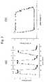
- FIG. 1is a schematic plot of two switchable thin film devices, being two-terminal, buffered-EPIR devices: a) with one buffer layer; b) with two buffer layers.
- FIGS. 2 a and 2 bare graphs showing the resistance change measurement of a PCMO (Pr 0.7 Ca 0.3 MnO 3 ) device without buffer layer in the test element.
- FIGS. 3 a and 3 bare graphs showing the resistance change measurement of the PCMO device with a YSZ (Yttrium Stabilized Zirconia—(ZrO 2 ) 0.92 (Y 2 O 3 ) 0.08 ) buffer layer.
- YSZYttrium Stabilized Zirconia—(ZrO 2 ) 0.92 (Y 2 O 3 ) 0.08 ) buffer layer.
- FIG. 4is a graph showing resistance change measurement of a YSZ layer alone, i.e., without the underlying PCMO perovskite switchable function layer.
- FIGS. 5 a and 5 bare graphs showing the resistance switch properties induced by electric pulses for a Sm—CeO 2 /PCMO/YBCO/LAO buffered-EPIR sample.
- FIGS. 6 a and 6 bare graphs showing resistance versus electric pulses for a PLZT/PCMO/YBCO/LAO buffered-EPIR memory sample.
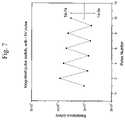
- FIG. 7is a graph showing resistance versus electric pulse number for a YSZ/PCMO/YBCO/LAO memory sample, where the electrical poling pulses have the same polarity (field from top electrode to low electrode). The switching of resistance was caused by pulses with short (100 ns) and long (10 ⁇ s) durations.
- buffer layersare added to an EPIR device to create a buffered-EPIR device.
- a bottom conductive electrode layer 12is used as the bottom electrode layer on substrate 11 .
- a thin top switchable function film, or layer, 14partially covers the bottom conductive electrode layer 12 .
- a bottom electrode contact pad 19is connected to the bottom conductive electrode layer 12 .
- the top switchable function layer 14is covered with a top buffer layer 15 .
- the top switchable function layer 14 and top buffer layer 15form a multi-layer structure 50 .
- a top electrode contact pad 16is fabricated on top of the top buffer layer 15 . Electrode contact pads 16 and 19 are connected to wires 17 and 18 , respectively.
- the conductive electrode layer 12 and the top electrode contact pad 16may be crystalline or polycrystalline conducting oxide or metallic layers.
- the individual components and their arrangements in the buffered-EPIR device with two buffer layersare the same as in FIG. 1 a , except that there is an additional thin bottom buffer layer 13 .
- the thin bottom buffer layer 13together with the switchable function layer 14 and the top buffer layer 15 , form a multi-layer structure 60 .
- the buffered-EPIR device of FIG. 1 acan also be an inverted structure where the buffer layer is deposited on the bottom electrode, and the top electrode contact is made to the switchable function layer.
- Multiple buffer layerscan be substituted for any of the single buffer layers in FIGS. 1 a and 1 b .
- Multiple switchable function layers with or without buffer layers in betweencan be substituted for single layers in FIGS. 1 a and 1 b.
- the preferred embodiment of the present inventionconsists of two conductive film layers as top-electrode and bottom electrode.
- Material of the conductive layercan be metal, alloy, conductive oxide, or other conductive materials, or their combination, e.g., Pt, RuO 2 , SrRuO 3 , IrO 2 , YBa 2 Cu 3 O7 ⁇ x (YBCO), La 1 ⁇ x Sr x CoO 3 (LSCO), SiC, carbon-tube, or their combinations.
- the bottom conductive electrode layer 12is deposited on an atomically ordered or polycrystalline substrate 11 , e.g., LaAlO 3 (LAO), SrTiO 3 (STO), MgO, Si, GaAs, TiN, etc., with or without the pre-existence of circuits on the substrate.
- the bottom electrode contact pad 19 and top electrode contact pad 16may be made of metal, conductive compounds and their combination, such as Ag, Au, Pt, Al, C, or other metal or alloy or a conducting oxide, and may be deposited by any variety of techniques onto the bottom conductive electrode layer 12 and top buffer layer 15 , as well as the top switchable function layer 14 , depending on device design.
- the switchable function layer 14is made of a perovskite-related material, such as colossal magneto-resistance (CMR) materials and their parent Mott insulator materials, High transition Temperature Superconducting (HTSC) material families (such as YBa 2 Cu 3 O 7 ⁇ x -based (YBCO) and Bi—Sr—Ca—Cu—O (“BSCCO”)), and the ACu3Ti 4 O 12 family of compounds (where A is a trivalent and/or rare earth ion) with thickness in the range from about one nanometer to about several micrometers.
- CMRcolossal magneto-resistance
- HTSCHigh transition Temperature Superconducting
- YBCOYBa 2 Cu 3 O 7 ⁇ x -based
- BSCCOBi—Sr—Ca—Cu—O
- ACu3Ti 4 O 12 family of compoundswhere A is a trivalent and/or rare earth ion
- stoichiometric perovskitessuch as (La,Pr)(CaPb)MnO 3
- HTSC materialsare YBCO and the Bi 2 Sr 2 Ca 2 Cu 3 O x -based (BSCCO) materials as well as other phases of these materials.
- the examples of the ACu 3 Ti 4 O 12 compoundare CaCu 3 Ti 4 O 12 , YCu 3 Ti 4 O 12 , and GdCu 3 Ti 3 FeO 12 .
- buffer layer 13is made of insulating materials consisting of single layer or multi-layer structure.
- Material for a buffer layercan be oxide or non-oxide with various lattice structures, including crystalline, polycrystalline, and glass.
- the oxide material for the buffermay be with or without perovskite lattice structure.
- Non-perovskite oxidessuch as SiO 2 , CeO 2 , MgO, ZnO, Y 2 O 3 , and their doped oxides, such as yittrium-stabled ZrO 2 (YSZ), (Sm,Gd) doped-CeO 2 , are examples, but others may be suitable.
- perovskite oxidesWhen perovskite oxides are used as buffer layers, they can be switchable or non-switchable insulating materials.
- These switchable perovskite-related oxide buffer layerscan be, but are not limited to, the high dielectric ACu 3 Ti 4 O 12 family, CMR materials and their non-doped parent Mott-insulator materials such as LaMnO 3 , and polar materials such as Ba 1 ⁇ x Sr x TiO 3 (BST), Pb(Zr,Ti)O 3 (PZT), La doped-PZT (PLZT), and Pb 3 Ge 5 O 11 (PGO).
- Non-oxide materialssuch as nitrides can also be used for the buffer layers 13 and 15 .
- the buffer layer thicknessis preferably in the range from approximately 1 nm to about 500 nm.
- an electric field and currentwill be created across the multi-layer structure 50 or 60 .
- a sufficiently high electric field strength and/or electric current densitycan change the charge distribution, and possibly the microstructures, and thus switch their states or modify properties such as the sensitivities to temperature, magnetic field, electric field, and mechanical pressure.
- the reversible resistance switching change in the buffered-EPIR devicescan be realized by applying short electric pulses to electrodes 16 and 19 .
- the asymmetric interface properties between the bottom electrode 19 and the switchable function layer 14 , and between the top electrode 16 and the switchable function layer 14can be induced or enhanced by adding the buffer layers and the corresponding film deposition processing.
- the buffer layermay be used on the top side or bottom side or both sides of the switchable function perovskite layer, shown as FIG. 1 a - b .
- the buffered interfaceis defined as the boundary of conductive electrode(s) and switchable perovskite film, which includes the thin buffer layer and the adjacent surface regions of both the electrode layer and switchable function layer in the buffered-EPIR devices.
- the thin buffer layersinterposed between the switchable function layer 14 and the electrodes 16 and 19 , can be used to modulate the barrier height, the density of electric carriers, carrier mobility, and/or carrier distribution in the interface area.
- the buffer layerscan also be selected to change carrier spin distribution and spin-alignment state in the interface region.
- the buffer layerscan be selected to change the chemical distribution and lattice structure at the interface as well as to modify electrical characteristics of the interface such as filament conduction.
- the buffer layerscan be selected to compensate temperature dependence of device resistance switching performance, and to enhance device radiation hardness.
- the additional interface asymmetry induced by the buffer layerscan enhance the reversible resistance switching properties of the buffered-EPIR device (resistor) from high-resistance state (R H ) to low resistance state (R L ) by voltage and current of short electric pulses, and to stabilize the properties of resistive switching and its non-volatility.
- adding the buffer layerscan be used to protect the device from being damaged or degraded by too large of energy shock by applied electric pulses, and to modify the non-volatile hysteresis loops to introduce more resistance states for multi-level memory application of the device.
- the buffer layerscan be made by various deposition techniques including rf-sputtering, e-beam evaporation, thermal evaporation, metal organic deposition, sol gel deposition, pulse laser deposition, and metal organic chemical vapor deposition, but not limited only to these techniques.
- FIG. 2shows the resistance change of a device without a buffer layer (in an EPIR device), using CMR material with composition of Pr 0.7 Ca 0.3 MnO 3 (PCMO) as the swichable active material.
- PCMOPr 0.7 Ca 0.3 MnO 3
- the PCMO film of 600 nm thicknesswas deposited on top of a YBCO bottom electrode layer of about 500 nm on a LaAlO 3 (100) substrate by pulse laser deposition (PLD) method.
- PLDpulse laser deposition
- the resistance of the sampleis measured with very small sensing current of ⁇ 1 ⁇ A, which does not switch the resistance of sample.
- the positive pulse directionis defined as from the top electrode to the bottom electrode.
- the switch ratio (R H ⁇ R L )/R L in this sampleis ⁇ 60%.
- FIG. 2 bis R vs. pulse-voltage hysteresis loop for the device measured after each pulse was applied. The resistance change after 5V-pulse is smaller than 10%.
- Device resistance Rreaches the low state after pulses of ⁇ +12V are applied.
- FIG. 3shows the resistance change versus electrical pulse number for the device of the present invention, a buffered-EPIR device, that is, a PCMO device with a YSZ buffer layer between top-electrode and the PCMO layer.
- the thin YSZ buffer layerwas deposited by PLD on the PCMO/YBCO/LAO, which was fabricated under the same growth conditions as the sample used in FIG. 2 .
- FIG. 3 ashows the device resistance switching under single pulses. The device resistance increases significantly after adding the insulating YSZ buffer layer. However, the voltage needed for switching the device is reduced to ⁇ 3V in comparison with the ⁇ 13V for the non buffered EPIR sample in FIG.
- FIG. 3 ais the non-volatile resistance hysteresis measurement, which shows the device switches under ⁇ 3V pulses. It also shows that a rapid transition to switching into the low or to high R states can be achieved by the buffered-EPIR system due to the nearly rectangular hysteresis loop. Again, the high R and low R states obtained in FIG. 3 b are not the same as in FIG. 3 a because of the multiple pulses applied in the measurement.
- the resistance switching properties of a YSZ buffer film without a PCMO active layer in an electrode/YSZ/electrode structurewas also studied in order to identify if the resistance switching behavior observed in the buffered-EPIR device was due only to the resistance switching of the YSZ buffer layer.
- the YSZ filmwas grown on YBCO/LAO substrate under the same conditions as the sample of FIG. 3 (where the YSZ film was used as a buffer layer and was deposited on PCMO on the YBCO/LAO substrate).
- the resistance of the YSZ film on YBCOcould be switched, but the switch ratio quickly decayed, as shown in FIG. 4 .
- the YSZ/YBCO samplerequired a much higher switching pulse voltage of ⁇ 7.3V as compared to the ⁇ 3V switch voltage needed for the YSZ/PCMO/YBCO sample shown in FIG. 3 .
- the PCMO layeris the major active switching layer in the YSZ buffered-EPIR device, and that the buffer layer does improve switching properties of the buffered-EPIR device.
- FIG. 5shows switching in the resistance versus electrical pulse number curve for a PCMO device with a Sm-doped CeO 2 buffer layer inserted between an Au top electrode and the PCMO switch layer in the buffered-EPIR device.
- Multiple pulseswere applied under plus and minus pulse polarity, with the device resistance changing by more than a factor of 4 under applied pulse voltage as low as ⁇ 2.7V. Such low switching voltage will allow the resistive device to be easily incorporated into semiconductor circuits.
- CCTO, PLZT, BST and PGO switchable materialscan also be used as the buffer layer in the present invention.
- the switchable perovskite materialcan be polar, such as PZT or PLZT, or non-polar material, such as CCTO.
- a buffered-EPIR device with a buffer PLZT layer inserted between the Ag top electrode and the PCMO layerwas switched to the low R L state ( ⁇ 9 k ⁇ ) by 4.7V pulses, and to the high R H state ( ⁇ 16 k ⁇ ) by ⁇ 6V pulses, as shown in FIG. 6 , yielding a switch ratio of ⁇ 80%.
- the buffered-EPIR device of the present inventionis different from existing ferroelectric switching devices.
- the non-volatile switching propertyis based on the two polarization states, or on dipole moment switching of the ferroelectric layer in the ferroelectric capacitor. This requires the ferroelectric layer to have large resistance (tens of mega ohm or higher) to hold charge separation.
- the ferroelectric buffer used in the buffered-EPIR device of the present inventionis a very thin (few nm) layer with low resistance (hundred Ohms to several kilo Ohms), and thus not supporting ferroelectric state retention.
- the non-volatile resistance switching properties of the buffered-EPIR devicewere obtained by applying across the device, positive and negative pulses alternatively, that is, bi-polar electric pulses.
- positive and negative pulsesalternatively, that is, bi-polar electric pulses.
- it may be more convenient to switch the device resistancei.e., increase or decrease resistance by single polarity pulses—only positive pulses or only negative pulses, uni-polar electric pulses with different durations, or with different intensities, or with different applied pulse numbers, or their combination.
- the non-volatile resistance of a YSZ/PCMO/YBCO/LAO samplewas switched by applying uni-polar electric pulses.
- Similar reversible resistance switching behaviormay be achieved not only by both positive pulses, but also by both negative pulses.
- the buffer/switchable-layer structureoffers great opportunity to modify the layer interface properties, and to modify the character of the hysteresis loop (the definition of the hysteresis has been explained in FIG. 2 b and FIG. 3 b ) of the buffered-EPIR device. These modifications can result in increased flexibility for applications of the reversible non-volatile resistor.
- One exampleis to modify the slope of the transition edge of the hysteresis loop. Sharpening the slope will benefit binary-state applications of the switchable resistor, while flattening the slope of the hysteresis curve will offer more multi-valued resistance states.
- the buffered-EPIR deviceinstead of the heterojunction buffer/switchable-function-layer/electrode described in FIG. 1 , it is also possible to use in the buffered-EPIR device a switchable perovskite multi-layer materials system with homojunction or gradient configurations, or their combination.
- the homojunction or gradient materialscan be fabricated by controlling doping of the layer materials and/or controlling the film deposition processing.
- a devicecan have a top-electrode/YSZ/PCMO structure, and use a graded PCMO film as the bottom electrode, if the lower part of the PCMO layer is doped to be conductive.
- a homojunction or gradient PCMO layercan even function as a complete buffer/PCMO/electrode component of a buffered-EPIR device.
- the devicecan be further simplified to be a top-electrode/homojunction or gradient PCMO layer directly on a substrate.
- the devicecan be used to make random access or read only memory devices with high data density and high read/write speed.
- Another application of this properties-modification method yielding the buffered-EPIR deviceis for a variable resistor that can be used in electronic circuits.
- Another application of this methodis to modify the characteristics of the device, to increase or decrease their detection sensitivities when they are used as sensors for temperature, magnetic field, electric field, and mechanical pressure. It is not intended that the descriptions above be regarded as limitations upon the present invention.
Landscapes
- Engineering & Computer Science (AREA)
- Chemical & Material Sciences (AREA)
- Materials Engineering (AREA)
- Microelectronics & Electronic Packaging (AREA)
- Physics & Mathematics (AREA)
- Electromagnetism (AREA)
- Semiconductor Memories (AREA)
- Hall/Mr Elements (AREA)
Abstract
Description
Claims (14)
Priority Applications (6)
| Application Number | Priority Date | Filing Date | Title |
|---|---|---|---|
| US11/034,695US7608467B2 (en) | 2004-01-13 | 2005-01-13 | Switchable resistive perovskite microelectronic device with multi-layer thin film structure |
| US12/586,143US7955871B2 (en) | 2004-01-13 | 2009-09-17 | Method of using a switchable resistive perovskite microelectronic device with multi-layer thin film structure |
| US12/586,147US8089111B2 (en) | 2004-01-13 | 2009-09-17 | Switchable two terminal multi-layer perovskite thin film resistive device and methods thereof |
| US13/068,884US8409879B2 (en) | 2004-01-13 | 2011-05-23 | Method of using a buffered electric pulse induced resistance device |
| US13/373,808US9218901B2 (en) | 2004-01-13 | 2011-12-01 | Two terminal multi-layer thin film resistance switching device with a diffusion barrier and methods thereof |
| US14/939,058US9349947B2 (en) | 2004-01-13 | 2015-11-12 | Methods of using a two terminal multi-layer thin film resistance switching device with a diffusion barrier |
Applications Claiming Priority (2)
| Application Number | Priority Date | Filing Date | Title |
|---|---|---|---|
| US53615504P | 2004-01-13 | 2004-01-13 | |
| US11/034,695US7608467B2 (en) | 2004-01-13 | 2005-01-13 | Switchable resistive perovskite microelectronic device with multi-layer thin film structure |
Related Child Applications (4)
| Application Number | Title | Priority Date | Filing Date |
|---|---|---|---|
| US12/586,147DivisionUS8089111B2 (en) | 2004-01-13 | 2009-09-17 | Switchable two terminal multi-layer perovskite thin film resistive device and methods thereof |
| US12/586,143ContinuationUS7955871B2 (en) | 2004-01-13 | 2009-09-17 | Method of using a switchable resistive perovskite microelectronic device with multi-layer thin film structure |
| US12/586,143DivisionUS7955871B2 (en) | 2004-01-13 | 2009-09-17 | Method of using a switchable resistive perovskite microelectronic device with multi-layer thin film structure |
| US13/373,808Continuation-In-PartUS9218901B2 (en) | 2004-01-13 | 2011-12-01 | Two terminal multi-layer thin film resistance switching device with a diffusion barrier and methods thereof |
Publications (2)
| Publication Number | Publication Date |
|---|---|
| US20050151156A1 US20050151156A1 (en) | 2005-07-14 |
| US7608467B2true US7608467B2 (en) | 2009-10-27 |
Family
ID=34742549
Family Applications (3)
| Application Number | Title | Priority Date | Filing Date |
|---|---|---|---|
| US11/034,695Active2027-02-25US7608467B2 (en) | 2004-01-13 | 2005-01-13 | Switchable resistive perovskite microelectronic device with multi-layer thin film structure |
| US12/586,147Expired - LifetimeUS8089111B2 (en) | 2004-01-13 | 2009-09-17 | Switchable two terminal multi-layer perovskite thin film resistive device and methods thereof |
| US12/586,143Expired - LifetimeUS7955871B2 (en) | 2004-01-13 | 2009-09-17 | Method of using a switchable resistive perovskite microelectronic device with multi-layer thin film structure |
Family Applications After (2)
| Application Number | Title | Priority Date | Filing Date |
|---|---|---|---|
| US12/586,147Expired - LifetimeUS8089111B2 (en) | 2004-01-13 | 2009-09-17 | Switchable two terminal multi-layer perovskite thin film resistive device and methods thereof |
| US12/586,143Expired - LifetimeUS7955871B2 (en) | 2004-01-13 | 2009-09-17 | Method of using a switchable resistive perovskite microelectronic device with multi-layer thin film structure |
Country Status (1)
| Country | Link |
|---|---|
| US (3) | US7608467B2 (en) |
Cited By (20)
| Publication number | Priority date | Publication date | Assignee | Title |
|---|---|---|---|---|
| US20100014344A1 (en)* | 2004-01-13 | 2010-01-21 | Board Of Regents, University Of Houston | Switchable two terminal multi-layer perovskite thin film resistive device and methods thereof |
| US20100032639A1 (en)* | 2008-08-07 | 2010-02-11 | Sandisk 3D Llc | Memory cell that includes a carbon-based memory element and methods of forming the same |
| US20100155953A1 (en)* | 2008-12-19 | 2010-06-24 | Unity Semiconductor Corporation | Conductive oxide electrodes |
| US20110188282A1 (en)* | 2010-02-02 | 2011-08-04 | Unity Semiconductor Corporation | Memory architectures and techniques to enhance throughput for cross-point arrays |
| US20110188281A1 (en)* | 2010-01-29 | 2011-08-04 | Unity Semiconductor Corporation | Local bit lines and methods of selecting the same to access memory elements in cross-point arrays |
| US20110304423A1 (en)* | 2004-01-13 | 2011-12-15 | Board Of Regents, University Of Houston | Method of using a buffered electric pulse induced resistance device |
| US20120087174A1 (en)* | 2004-09-03 | 2012-04-12 | Unity Semiconductor Corporation | Two Terminal Re Writeable Non Volatile Ion Transport Memory Device |
| US20120126195A1 (en)* | 2004-01-13 | 2012-05-24 | Board Of Regents, University Of Houston | Two terminal multi-layer thin film resistance switching device with a diffusion barrier and methods thereof |
| RU2468471C1 (en)* | 2011-04-07 | 2012-11-27 | Государственное образовательное учреждение высшего профессионального образования "Петрозаводский государственный университет" | Method of obtainment of nonvolatile storage element |
| US8536015B2 (en) | 2008-04-11 | 2013-09-17 | Sandisk 3D Llc | Memory cell that includes a carbon-based memory element and methods of forming the same |
| US8559209B2 (en) | 2011-06-10 | 2013-10-15 | Unity Semiconductor Corporation | Array voltage regulating technique to enable data operations on large cross-point memory arrays with resistive memory elements |
| US8565003B2 (en) | 2011-06-28 | 2013-10-22 | Unity Semiconductor Corporation | Multilayer cross-point memory array having reduced disturb susceptibility |
| RU2516771C1 (en)* | 2012-10-23 | 2014-05-20 | Федеральное государственное бюджетное учреждение науки Институт физики полупроводников им. А.В. Ржанова Сибирского отделения Российской академии наук (ИФП СО РАН) | Resistive flash memory element |
| US8866118B2 (en) | 2012-12-21 | 2014-10-21 | Intermolecular, Inc. | Morphology control of ultra-thin MeOx layer |
| US8891276B2 (en) | 2011-06-10 | 2014-11-18 | Unity Semiconductor Corporation | Memory array with local bitlines and local-to-global bitline pass gates and gain stages |
| US8937292B2 (en) | 2011-08-15 | 2015-01-20 | Unity Semiconductor Corporation | Vertical cross point arrays for ultra high density memory applications |
| US9117495B2 (en) | 2011-06-10 | 2015-08-25 | Unity Semiconductor Corporation | Global bit line pre-charge circuit that compensates for process, operating voltage, and temperature variations |
| US9159408B2 (en) | 2004-02-06 | 2015-10-13 | Unity Semiconductor Corporation | Memory element with a reactive metal layer |
| US9484533B2 (en) | 2005-03-30 | 2016-11-01 | Unity Semiconductor Corporation | Multi-layered conductive metal oxide structures and methods for facilitating enhanced performance characteristics of two-terminal memory cells |
| US10566056B2 (en) | 2011-06-10 | 2020-02-18 | Unity Semiconductor Corporation | Global bit line pre-charge circuit that compensates for process, operating voltage, and temperature variations |
Families Citing this family (53)
| Publication number | Priority date | Publication date | Assignee | Title |
|---|---|---|---|---|
| US7009235B2 (en)* | 2003-11-10 | 2006-03-07 | Unity Semiconductor Corporation | Conductive memory stack with non-uniform width |
| US6753561B1 (en) | 2002-08-02 | 2004-06-22 | Unity Semiconductor Corporation | Cross point memory array using multiple thin films |
| US6917539B2 (en)* | 2002-08-02 | 2005-07-12 | Unity Semiconductor Corporation | High-density NVRAM |
| US6906939B2 (en)* | 2002-08-02 | 2005-06-14 | Unity Semiconductor Corporation | Re-writable memory with multiple memory layers |
| US7057914B2 (en)* | 2002-08-02 | 2006-06-06 | Unity Semiconductor Corporation | Cross point memory array with fast access time |
| US6859382B2 (en)* | 2002-08-02 | 2005-02-22 | Unity Semiconductor Corporation | Memory array of a non-volatile ram |
| US6831854B2 (en)* | 2002-08-02 | 2004-12-14 | Unity Semiconductor Corporation | Cross point memory array using distinct voltages |
| US6970375B2 (en)* | 2002-08-02 | 2005-11-29 | Unity Semiconductor Corporation | Providing a reference voltage to a cross point memory array |
| US7309616B2 (en) | 2003-03-13 | 2007-12-18 | Unity Semiconductor Corporation | Laser annealing of complex metal oxides (CMO) memory materials for non-volatile memory integrated circuits |
| US7099179B2 (en)* | 2003-12-22 | 2006-08-29 | Unity Semiconductor Corporation | Conductive memory array having page mode and burst mode write capability |
| US7538338B2 (en)* | 2004-09-03 | 2009-05-26 | Unity Semiconductor Corporation | Memory using variable tunnel barrier widths |
| US7060586B2 (en)* | 2004-04-30 | 2006-06-13 | Sharp Laboratories Of America, Inc. | PCMO thin film with resistance random access memory (RRAM) characteristics |
| EP1775774A4 (en)* | 2004-06-11 | 2008-10-22 | Matsushita Electric Industrial Co Ltd | POWER ELEMENT |
| US20060000542A1 (en)* | 2004-06-30 | 2006-01-05 | Yongki Min | Metal oxide ceramic thin film on base metal electrode |
| JP4365737B2 (en)* | 2004-06-30 | 2009-11-18 | シャープ株式会社 | Method of driving variable resistance element and storage device |
| US7075817B2 (en) | 2004-07-20 | 2006-07-11 | Unity Semiconductor Corporation | Two terminal memory array having reference cells |
| US7290315B2 (en)* | 2004-10-21 | 2007-11-06 | Intel Corporation | Method for making a passive device structure |
| US20060099803A1 (en)* | 2004-10-26 | 2006-05-11 | Yongki Min | Thin film capacitor |
| US7464621B2 (en)* | 2004-11-09 | 2008-12-16 | Steeda Autosports, Inc. | Longitudinally displaced shifter |
| US7327600B2 (en)* | 2004-12-23 | 2008-02-05 | Unity Semiconductor Corporation | Storage controller for multiple configurations of vertical memory |
| US7375412B1 (en)* | 2005-03-31 | 2008-05-20 | Intel Corporation | iTFC with optimized C(T) |
| US20060220177A1 (en)* | 2005-03-31 | 2006-10-05 | Palanduz Cengiz A | Reduced porosity high-k thin film mixed grains for thin film capacitor applications |
| US7629269B2 (en)* | 2005-03-31 | 2009-12-08 | Intel Corporation | High-k thin film grain size control |
| US7453144B2 (en)* | 2005-06-29 | 2008-11-18 | Intel Corporation | Thin film capacitors and methods of making the same |
| US7978047B2 (en)* | 2005-08-29 | 2011-07-12 | Sharp Kabushiki Kaisha | Variable resistor element and its manufacturing method |
| US20070045694A1 (en)* | 2005-08-30 | 2007-03-01 | Sharp Laboratories Of America, Inc. | Method of selecting a RRAM memory material and electrode material |
| US8106375B2 (en)* | 2005-11-30 | 2012-01-31 | The Trustees Of The University Of Pennsylvania | Resistance-switching memory based on semiconductor composition of perovskite conductor doped perovskite insulator |
| US7666526B2 (en)* | 2005-11-30 | 2010-02-23 | The Trustees Of The University Of Pennsylvania | Non-volatile resistance-switching oxide thin film devices |
| KR101275800B1 (en)* | 2006-04-28 | 2013-06-18 | 삼성전자주식회사 | Non-volatile memory device comprising variable resistance material |
| US7522468B2 (en)* | 2006-06-08 | 2009-04-21 | Unity Semiconductor Corporation | Serial memory interface |
| US7747817B2 (en)* | 2006-06-28 | 2010-06-29 | Unity Semiconductor Corporation | Performing data operations using non-volatile third dimension memory |
| US20080011996A1 (en)* | 2006-07-11 | 2008-01-17 | Johannes Georg Bednorz | Multi-layer device with switchable resistance |
| JP2008028228A (en)* | 2006-07-24 | 2008-02-07 | Seiko Epson Corp | Variable resistance element and resistance change type memory device |
| US7619945B2 (en) | 2006-08-18 | 2009-11-17 | Unity Semiconductor Corporation | Memory power management |
| US7539811B2 (en) | 2006-10-05 | 2009-05-26 | Unity Semiconductor Corporation | Scaleable memory systems using third dimension memory |
| US7379364B2 (en)* | 2006-10-19 | 2008-05-27 | Unity Semiconductor Corporation | Sensing a signal in a two-terminal memory array having leakage current |
| US7372753B1 (en)* | 2006-10-19 | 2008-05-13 | Unity Semiconductor Corporation | Two-cycle sensing in a two-terminal memory array having leakage current |
| TWI340473B (en)* | 2007-01-12 | 2011-04-11 | Winbond Electronics Corp | Nonvolatile memory and fabrication method thereof |
| US7765380B2 (en)* | 2007-01-19 | 2010-07-27 | Unity Semiconductor Corporation | Fast data access through page manipulation |
| US7777215B2 (en)* | 2007-07-20 | 2010-08-17 | Macronix International Co., Ltd. | Resistive memory structure with buffer layer |
| JP5501966B2 (en)* | 2007-07-25 | 2014-05-28 | インターモレキュラー, インコーポレイテッド | Multi-state non-volatile memory device |
| US7616089B2 (en)* | 2007-09-28 | 2009-11-10 | Cirrus Logic, Inc. | Compensation of field effect on polycrystalline resistors |
| US7910929B2 (en)* | 2007-12-18 | 2011-03-22 | Semiconductor Energy Laboratory Co., Ltd. | Semiconductor device |
| TWI356488B (en)* | 2008-03-26 | 2012-01-11 | Univ Nat Chiao Tung | Memory device and method of manufacturing the same |
| US8004874B2 (en)* | 2008-08-06 | 2011-08-23 | Seagate Technology Llc | Multi-terminal resistance device |
| US8304754B2 (en)* | 2008-11-12 | 2012-11-06 | Sandisk 3D Llc | Metal oxide materials and electrodes for Re-RAM |
| US20100135061A1 (en)* | 2008-12-02 | 2010-06-03 | Shaoping Li | Non-Volatile Memory Cell with Ferroelectric Layer Configurations |
| WO2010064444A1 (en)* | 2008-12-05 | 2010-06-10 | パナソニック株式会社 | Nonvolatile memory element and manufacturing method therefor |
| WO2011047393A1 (en)* | 2009-10-16 | 2011-04-21 | President And Fellows Of Harvard College | Field tunable solid state ionic-electronic switches |
| JP4669567B1 (en)* | 2010-02-24 | 2011-04-13 | エンパイア テクノロジー ディベロップメント エルエルシー | Wiring board and manufacturing method thereof |
| KR101744758B1 (en)* | 2010-08-31 | 2017-06-09 | 삼성전자 주식회사 | Nonvolatile memory element and memory device including the same |
| CN103500797B (en)* | 2013-10-17 | 2016-09-07 | 北京科技大学 | Random access memory unit and manufacture method thereof |
| US11610941B2 (en)* | 2020-11-25 | 2023-03-21 | International Business Machines Corporation | Integrated non volatile memory electrode thin film resistor cap and etch stop |
Citations (6)
| Publication number | Priority date | Publication date | Assignee | Title |
|---|---|---|---|---|
| US5274249A (en)* | 1991-12-20 | 1993-12-28 | University Of Maryland | Superconducting field effect devices with thin channel layer |
| US5527567A (en)* | 1994-09-02 | 1996-06-18 | Ceram Incorporated | Metalorganic chemical vapor deposition of layered structure oxides |
| US6204139B1 (en)* | 1998-08-25 | 2001-03-20 | University Of Houston | Method for switching the properties of perovskite materials used in thin film resistors |
| US6653703B2 (en)* | 2001-04-20 | 2003-11-25 | Kabushiki Kaisha Toshiba | Semiconductor memory device using magneto resistive element and method of manufacturing the same |
| US20040159828A1 (en)* | 2002-08-02 | 2004-08-19 | Unity Semiconductor, Inc. | Resistive memory device with a treated interface |
| US7029924B2 (en)* | 2003-09-05 | 2006-04-18 | Sharp Laboratories Of America, Inc. | Buffered-layer memory cell |
Family Cites Families (1)
| Publication number | Priority date | Publication date | Assignee | Title |
|---|---|---|---|---|
| US7608467B2 (en)* | 2004-01-13 | 2009-10-27 | Board of Regents University of Houston | Switchable resistive perovskite microelectronic device with multi-layer thin film structure |
- 2005
- 2005-01-13USUS11/034,695patent/US7608467B2/enactiveActive
- 2009
- 2009-09-17USUS12/586,147patent/US8089111B2/ennot_activeExpired - Lifetime
- 2009-09-17USUS12/586,143patent/US7955871B2/ennot_activeExpired - Lifetime
Patent Citations (6)
| Publication number | Priority date | Publication date | Assignee | Title |
|---|---|---|---|---|
| US5274249A (en)* | 1991-12-20 | 1993-12-28 | University Of Maryland | Superconducting field effect devices with thin channel layer |
| US5527567A (en)* | 1994-09-02 | 1996-06-18 | Ceram Incorporated | Metalorganic chemical vapor deposition of layered structure oxides |
| US6204139B1 (en)* | 1998-08-25 | 2001-03-20 | University Of Houston | Method for switching the properties of perovskite materials used in thin film resistors |
| US6653703B2 (en)* | 2001-04-20 | 2003-11-25 | Kabushiki Kaisha Toshiba | Semiconductor memory device using magneto resistive element and method of manufacturing the same |
| US20040159828A1 (en)* | 2002-08-02 | 2004-08-19 | Unity Semiconductor, Inc. | Resistive memory device with a treated interface |
| US7029924B2 (en)* | 2003-09-05 | 2006-04-18 | Sharp Laboratories Of America, Inc. | Buffered-layer memory cell |
Non-Patent Citations (2)
| Title |
|---|
| "Electric-pulse-induced Reversible Resistance Change Effect in Magnetoresistive Films", S.Q. Liu, et al., Appl. Phys. Lett., vol. 76, pp. 2749-2751, 2000. |
| "Growth, Transport, and Magnetic Properties of Pr0.67 Ca0.33MnO3 Thin Films", S. K. Singh, et al, Appl. Phys. Lett., vol. 69, pp. 263-265, 1996. |
Cited By (70)
| Publication number | Priority date | Publication date | Assignee | Title |
|---|---|---|---|---|
| US8409879B2 (en)* | 2004-01-13 | 2013-04-02 | Board Of Regents, University Of Houston | Method of using a buffered electric pulse induced resistance device |
| US20110304423A1 (en)* | 2004-01-13 | 2011-12-15 | Board Of Regents, University Of Houston | Method of using a buffered electric pulse induced resistance device |
| US20160064660A1 (en)* | 2004-01-13 | 2016-03-03 | Board Of Regents, University Of Houston | Methods of Using A Two Terminal Multi-Layer Thin Film Resistance Switching Device With A Diffusion Barrier |
| US20100134239A1 (en)* | 2004-01-13 | 2010-06-03 | Board Of Regents, University Of Houston | Method of using a switchable resistive perovskite microelectronic device with multi-Layer thin film structure |
| US20100014344A1 (en)* | 2004-01-13 | 2010-01-21 | Board Of Regents, University Of Houston | Switchable two terminal multi-layer perovskite thin film resistive device and methods thereof |
| US7955871B2 (en)* | 2004-01-13 | 2011-06-07 | Board Of Regents, University Of Houston | Method of using a switchable resistive perovskite microelectronic device with multi-layer thin film structure |
| US9349947B2 (en)* | 2004-01-13 | 2016-05-24 | Board Of Regents, University Of Houston | Methods of using a two terminal multi-layer thin film resistance switching device with a diffusion barrier |
| US9218901B2 (en)* | 2004-01-13 | 2015-12-22 | Board Of Regents, University Of Houston | Two terminal multi-layer thin film resistance switching device with a diffusion barrier and methods thereof |
| US20120126195A1 (en)* | 2004-01-13 | 2012-05-24 | Board Of Regents, University Of Houston | Two terminal multi-layer thin film resistance switching device with a diffusion barrier and methods thereof |
| US8089111B2 (en)* | 2004-01-13 | 2012-01-03 | Board Of Regents, University Of Houston | Switchable two terminal multi-layer perovskite thin film resistive device and methods thereof |
| US10833125B2 (en) | 2004-02-06 | 2020-11-10 | Hefei Reliance Memory Limited | Memory element with a reactive metal layer |
| US11672189B2 (en) | 2004-02-06 | 2023-06-06 | Hefei Reliance Memory Limited | Two-terminal reversibly switchable memory device |
| US10680171B2 (en) | 2004-02-06 | 2020-06-09 | Hefei Reliance Memory Limited | Two-terminal reversibly switchable memory device |
| US10224480B2 (en) | 2004-02-06 | 2019-03-05 | Hefei Reliance Memory Limited | Two-terminal reversibly switchable memory device |
| US10340312B2 (en) | 2004-02-06 | 2019-07-02 | Hefei Reliance Memory Limited | Memory element with a reactive metal layer |
| US9159913B2 (en) | 2004-02-06 | 2015-10-13 | Unity Semiconductor Corporation | Two-terminal reversibly switchable memory device |
| US11063214B2 (en) | 2004-02-06 | 2021-07-13 | Hefei Reliance Memory Limited | Two-terminal reversibly switchable memory device |
| US9831425B2 (en) | 2004-02-06 | 2017-11-28 | Unity Semiconductor Corporation | Two-terminal reversibly switchable memory device |
| US9159408B2 (en) | 2004-02-06 | 2015-10-13 | Unity Semiconductor Corporation | Memory element with a reactive metal layer |
| US9806130B2 (en) | 2004-02-06 | 2017-10-31 | Unity Semiconductor Corporation | Memory element with a reactive metal layer |
| US11502249B2 (en) | 2004-02-06 | 2022-11-15 | Hefei Reliance Memory Limited | Memory element with a reactive metal layer |
| US9570515B2 (en) | 2004-02-06 | 2017-02-14 | Unity Semiconductor Corporation | Memory element with a reactive metal layer |
| US20120087174A1 (en)* | 2004-09-03 | 2012-04-12 | Unity Semiconductor Corporation | Two Terminal Re Writeable Non Volatile Ion Transport Memory Device |
| US10002646B2 (en) | 2005-03-30 | 2018-06-19 | Unity Semiconductor Corporation | Local bit lines and methods of selecting the same to access memory elements in cross-point arrays |
| US9401202B2 (en) | 2005-03-30 | 2016-07-26 | Unity Semiconductor Corporation | Array voltage regulating technique to enable data operations on large memory arrays with resistive memory elements |
| US8929126B2 (en) | 2005-03-30 | 2015-01-06 | Unity Semiconductor Corporation | Array voltage regulating technique to enable data operations on large cross-point memory arrays with resistive memory elements |
| US9484533B2 (en) | 2005-03-30 | 2016-11-01 | Unity Semiconductor Corporation | Multi-layered conductive metal oxide structures and methods for facilitating enhanced performance characteristics of two-terminal memory cells |
| US9720611B2 (en) | 2005-03-30 | 2017-08-01 | Unity Semiconductor Corporation | Array voltage regulating technique to enable data operations on large memory arrays with resistive memory elements |
| US9818799B2 (en) | 2005-03-30 | 2017-11-14 | Unity Semiconductor Corporation | Multi-layered conductive metal oxide structures and methods for facilitating enhanced performance characteristics of two-terminal memory cells |
| US8536015B2 (en) | 2008-04-11 | 2013-09-17 | Sandisk 3D Llc | Memory cell that includes a carbon-based memory element and methods of forming the same |
| US8557685B2 (en) | 2008-08-07 | 2013-10-15 | Sandisk 3D Llc | Memory cell that includes a carbon-based memory element and methods of forming the same |
| US20100032639A1 (en)* | 2008-08-07 | 2010-02-11 | Sandisk 3D Llc | Memory cell that includes a carbon-based memory element and methods of forming the same |
| US20100032643A1 (en)* | 2008-08-07 | 2010-02-11 | Sandisk 3D Llc | Memory cell that includes a carbon-based memory element and methods of forming the same |
| US8390100B2 (en) | 2008-12-19 | 2013-03-05 | Unity Semiconductor Corporation | Conductive oxide electrodes |
| US20100155953A1 (en)* | 2008-12-19 | 2010-06-24 | Unity Semiconductor Corporation | Conductive oxide electrodes |
| US11398256B2 (en) | 2010-01-29 | 2022-07-26 | Unity Semiconductor Corporation | Local bit lines and methods of selecting the same to access memory elements in cross-point arrays |
| US8897050B2 (en) | 2010-01-29 | 2014-11-25 | Unity Semiconductor Corporation | Local bit lines and methods of selecting the same to access memory elements in cross-point arrays |
| US20110188281A1 (en)* | 2010-01-29 | 2011-08-04 | Unity Semiconductor Corporation | Local bit lines and methods of selecting the same to access memory elements in cross-point arrays |
| US10622028B2 (en) | 2010-01-29 | 2020-04-14 | Unity Semiconductor Corporation | Local bit lines and methods of selecting the same to access memory elements in cross-point arrays |
| US8270193B2 (en) | 2010-01-29 | 2012-09-18 | Unity Semiconductor Corporation | Local bit lines and methods of selecting the same to access memory elements in cross-point arrays |
| US20110188282A1 (en)* | 2010-02-02 | 2011-08-04 | Unity Semiconductor Corporation | Memory architectures and techniques to enhance throughput for cross-point arrays |
| US8638584B2 (en) | 2010-02-02 | 2014-01-28 | Unity Semiconductor Corporation | Memory architectures and techniques to enhance throughput for cross-point arrays |
| RU2468471C1 (en)* | 2011-04-07 | 2012-11-27 | Государственное образовательное учреждение высшего профессионального образования "Петрозаводский государственный университет" | Method of obtainment of nonvolatile storage element |
| US10229739B2 (en) | 2011-06-10 | 2019-03-12 | Unity Semiconductor Corporation | Global bit line pre-charge circuit that compensates for process, operating voltage, and temperature variations |
| US11144218B2 (en) | 2011-06-10 | 2021-10-12 | Unity Semiconductor Corporation | Array voltage regulating technique to enable data operations on large memory arrays with resistive memory elements |
| US8559209B2 (en) | 2011-06-10 | 2013-10-15 | Unity Semiconductor Corporation | Array voltage regulating technique to enable data operations on large cross-point memory arrays with resistive memory elements |
| US10031686B2 (en) | 2011-06-10 | 2018-07-24 | Unity Semiconductor Corporation | Array voltage regulating technique to enable data operations on large memory arrays with resistive memory elements |
| US9390796B2 (en) | 2011-06-10 | 2016-07-12 | Unity Semiconductor Corporation | Global bit line pre-charge circuit that compensates for process, operating voltage, and temperature variations |
| US9870823B2 (en) | 2011-06-10 | 2018-01-16 | Unity Semiconductor Corporation | Global bit line pre-charge circuit that compensates for process, operating voltage, and temperature variations |
| US9117495B2 (en) | 2011-06-10 | 2015-08-25 | Unity Semiconductor Corporation | Global bit line pre-charge circuit that compensates for process, operating voltage, and temperature variations |
| US11087841B2 (en) | 2011-06-10 | 2021-08-10 | Unity Semiconductor Corporation | Global bit line pre-charge circuit that compensates for process, operating voltage, and temperature variations |
| US8891276B2 (en) | 2011-06-10 | 2014-11-18 | Unity Semiconductor Corporation | Memory array with local bitlines and local-to-global bitline pass gates and gain stages |
| US10566056B2 (en) | 2011-06-10 | 2020-02-18 | Unity Semiconductor Corporation | Global bit line pre-charge circuit that compensates for process, operating voltage, and temperature variations |
| US10585603B2 (en) | 2011-06-10 | 2020-03-10 | Unity Semiconductor Corporation | Array voltage regulating technique to enable data operations on large memory arrays with resistive memory elements |
| US9691480B2 (en) | 2011-06-10 | 2017-06-27 | Unity Semiconductor Corporation | Global bit line pre-charge circuit that compensates for process, operating voltage, and temperature variations |
| US10788993B2 (en) | 2011-06-10 | 2020-09-29 | Unity Semiconductor Corporation | Array voltage regulating technique to enable data operations on large memory arrays with resistive memory elements |
| US8565003B2 (en) | 2011-06-28 | 2013-10-22 | Unity Semiconductor Corporation | Multilayer cross-point memory array having reduced disturb susceptibility |
| US11367751B2 (en) | 2011-08-15 | 2022-06-21 | Unity Semiconductor Corporation | Vertical cross-point arrays for ultra-high-density memory applications |
| US10790334B2 (en) | 2011-08-15 | 2020-09-29 | Unity Semiconductor Corporation | Vertical cross-point arrays for ultra-high-density memory applications |
| US11849593B2 (en) | 2011-08-15 | 2023-12-19 | Unity Semiconductor Corporation | Vertical cross-point arrays for ultra-high-density memory applications |
| US9691821B2 (en) | 2011-08-15 | 2017-06-27 | Unity Semiconductor Corporation | Vertical cross-point arrays for ultra-high-density memory applications |
| US9312307B2 (en) | 2011-08-15 | 2016-04-12 | Unity Semiconductor Corporation | Vertical cross point arrays for ultra high density memory applications |
| US8937292B2 (en) | 2011-08-15 | 2015-01-20 | Unity Semiconductor Corporation | Vertical cross point arrays for ultra high density memory applications |
| US11037987B2 (en) | 2011-09-30 | 2021-06-15 | Hefei Reliance Memory Limited | Multi-layered conductive metal oxide structures and methods for facilitating enhanced performance characteristics of two-terminal memory cells |
| US11289542B2 (en) | 2011-09-30 | 2022-03-29 | Hefei Reliance Memory Limited | Multi-layered conductive metal oxide structures and methods for facilitating enhanced performance characteristics of two-terminal memory cells |
| US10186553B2 (en) | 2011-09-30 | 2019-01-22 | Hefei Reliance Memory Limited | Multi-layered conductive metal oxide structures and methods for facilitating enhanced performance characteristics of two-terminal memory cells |
| US10535714B2 (en) | 2011-09-30 | 2020-01-14 | Hefei Reliance Memory Limited | Multi-layered conductive metal oxide structures and methods for facilitating enhanced performance characteristics of two-terminal memory cells |
| US11765914B2 (en) | 2011-09-30 | 2023-09-19 | Hefei Reliance Memory Limited | Multi-layered conductive metal oxide structures and methods for facilitating enhanced performance characteristics of two-terminal memory cells |
| RU2516771C1 (en)* | 2012-10-23 | 2014-05-20 | Федеральное государственное бюджетное учреждение науки Институт физики полупроводников им. А.В. Ржанова Сибирского отделения Российской академии наук (ИФП СО РАН) | Resistive flash memory element |
| US8866118B2 (en) | 2012-12-21 | 2014-10-21 | Intermolecular, Inc. | Morphology control of ultra-thin MeOx layer |
Also Published As
| Publication number | Publication date |
|---|---|
| US20100134239A1 (en) | 2010-06-03 |
| US8089111B2 (en) | 2012-01-03 |
| US20050151156A1 (en) | 2005-07-14 |
| US20100014344A1 (en) | 2010-01-21 |
| US7955871B2 (en) | 2011-06-07 |
Similar Documents
| Publication | Publication Date | Title |
|---|---|---|
| US7608467B2 (en) | Switchable resistive perovskite microelectronic device with multi-layer thin film structure | |
| US9349947B2 (en) | Methods of using a two terminal multi-layer thin film resistance switching device with a diffusion barrier | |
| US6204139B1 (en) | Method for switching the properties of perovskite materials used in thin film resistors | |
| US8687401B2 (en) | Ferro-resistive random access memory (Ferro-RRAM), operation method and manufacturing method thereof | |
| US6762481B2 (en) | Electrically programmable nonvolatile variable capacitor | |
| Liu et al. | Electric-pulse-induced reversible resistance change effect in magnetoresistive films | |
| US8023309B2 (en) | Semiconductor memory device, method for fabricating the same and semiconductor switching device | |
| US6815744B1 (en) | Microelectronic device for storing information with switchable ohmic resistance | |
| Beck et al. | Reproducible switching effect in thin oxide films for memory applications | |
| Lee et al. | Built-in voltages and asymmetric polarization switching in Pb (Zr, Ti) O 3 thin film capacitors | |
| US20080011996A1 (en) | Multi-layer device with switchable resistance | |
| US20100135061A1 (en) | Non-Volatile Memory Cell with Ferroelectric Layer Configurations | |
| US20040161888A1 (en) | Multi-resistive state material that uses dopants | |
| RU2468471C1 (en) | Method of obtainment of nonvolatile storage element | |
| WO2006101152A1 (en) | Nonvolatile memory element | |
| Guerrero et al. | Growth and characterization of epitaxial ferroelectric PbZrxTi1− xO3 thin film capacitors with SrRuO3 electrodes for non-volatile memory applications | |
| US8409879B2 (en) | Method of using a buffered electric pulse induced resistance device | |
| US20150364536A1 (en) | Device comprising a plurality of thin layers | |
| CN112567542B (en) | Nonvolatile memory cell | |
| Okano et al. | Nonvolatile programmable two-terminal diodes using a ferroelectric semiconductor | |
| JP2007067402A (en) | RRAM memory material and electrode material selection method | |
| GAGOU et al. | Chap. 26-Resistance Switching Effect in Octahedral framework oxide | |
| Sharma et al. | Bipolar resistive switching in magnetostrictive Ni/PZT/Pt structure for non-volatile memory applications | |
| Hsu et al. | Interface-engineered resistive switching in Ag/SrTiO3/Nd0. 7Ca0. 3MnO3/YBa2Cu3O7 heterostructures | |
| CN101436546A (en) | Method for altering oxide material physical properties |
Legal Events
| Date | Code | Title | Description |
|---|---|---|---|
| AS | Assignment | Owner name:BOARD OF REGENTS, UNIVERSITY OF HOUSTON, TEXAS Free format text:ASSIGNMENT OF ASSIGNORS INTEREST;ASSIGNORS:WU, NAIJUAN;CHEN, XIN;IGNATIEV, ALEX;REEL/FRAME:016364/0908 Effective date:20050201 | |
| AS | Assignment | Owner name:BOARD OF REGENTS, UNIVERSITY OF HOUSTON, TEXAS Free format text:ASSIGNMENT OF ASSIGNORS INTEREST;ASSIGNORS:WU, NAIJUAN;CHEN, XIN;IGNATIEV, ALEX;REEL/FRAME:023303/0159 Effective date:20050201 | |
| STCF | Information on status: patent grant | Free format text:PATENTED CASE | |
| CC | Certificate of correction | ||
| AS | Assignment | Owner name:BOARD OF REGENTS, UNIVERSITY OF HOUSTON, TEXAS Free format text:ASSIGNMENT OF ASSIGNORS INTEREST;ASSIGNORS:WU, NAIJUAN;CHEN, XIN;IGNATIEV, ALEX;REEL/FRAME:026450/0272 Effective date:20050201 | |
| FPAY | Fee payment | Year of fee payment:4 | |
| AS | Assignment | Owner name:UNIVERSITY OF HOUSTON SYSTEM, TEXAS Free format text:ASSIGNMENT OF ASSIGNORS INTEREST;ASSIGNOR:BOARD OF REGENTS, UNIVERSITY OF HOUSTON;REEL/FRAME:042269/0232 Effective date:20170308 | |
| FPAY | Fee payment | Year of fee payment:8 | |
| MAFP | Maintenance fee payment | Free format text:PAYMENT OF MAINTENANCE FEE, 12TH YR, SMALL ENTITY (ORIGINAL EVENT CODE: M2553); ENTITY STATUS OF PATENT OWNER: SMALL ENTITY Year of fee payment:12 | |
| AS | Assignment | Owner name:UNIVERSITY OF HOUSTON SYSTEM, TEXAS Free format text:CORRECTIVE ASSIGNMENT TO CORRECT THE PATENT NUMBER 8,090,111 TO 8,089,111 PREVIOUSLY RECORDED AT REEL: 042269 FRAME: 0232. ASSIGNOR(S) HEREBY CONFIRMS THE ASSIGNMENT;ASSIGNOR:BOARD OF REGENTS, UNIVERSITY OF HOUSTON;REEL/FRAME:066354/0676 Effective date:20170308 |