US7606098B2 - Semiconductor memory array architecture with grouped memory cells, and method of controlling same - Google Patents
Semiconductor memory array architecture with grouped memory cells, and method of controlling sameDownload PDFInfo
- Publication number
- US7606098B2 US7606098B2US11/787,718US78771807AUS7606098B2US 7606098 B2US7606098 B2US 7606098B2US 78771807 AUS78771807 AUS 78771807AUS 7606098 B2US7606098 B2US 7606098B2
- Authority
- US
- United States
- Prior art keywords
- circuitry
- memory cells
- word line
- memory cell
- group
- Prior art date
- Legal status (The legal status is an assumption and is not a legal conclusion. Google has not performed a legal analysis and makes no representation as to the accuracy of the status listed.)
- Active, expires
Links
Images


Classifications
- H—ELECTRICITY
- H10—SEMICONDUCTOR DEVICES; ELECTRIC SOLID-STATE DEVICES NOT OTHERWISE PROVIDED FOR
- H10B—ELECTRONIC MEMORY DEVICES
- H10B12/00—Dynamic random access memory [DRAM] devices
- H—ELECTRICITY
- H10—SEMICONDUCTOR DEVICES; ELECTRIC SOLID-STATE DEVICES NOT OTHERWISE PROVIDED FOR
- H10B—ELECTRONIC MEMORY DEVICES
- H10B12/00—Dynamic random access memory [DRAM] devices
- H10B12/20—DRAM devices comprising floating-body transistors, e.g. floating-body cells
- H—ELECTRICITY
- H10—SEMICONDUCTOR DEVICES; ELECTRIC SOLID-STATE DEVICES NOT OTHERWISE PROVIDED FOR
- H10B—ELECTRONIC MEMORY DEVICES
- H10B12/00—Dynamic random access memory [DRAM] devices
- H10B12/50—Peripheral circuit region structures
- H—ELECTRICITY
- H10—SEMICONDUCTOR DEVICES; ELECTRIC SOLID-STATE DEVICES NOT OTHERWISE PROVIDED FOR
- H10D—INORGANIC ELECTRIC SEMICONDUCTOR DEVICES
- H10D30/00—Field-effect transistors [FET]
- H10D30/60—Insulated-gate field-effect transistors [IGFET]
- H10D30/711—Insulated-gate field-effect transistors [IGFET] having floating bodies
- H—ELECTRICITY
- H10—SEMICONDUCTOR DEVICES; ELECTRIC SOLID-STATE DEVICES NOT OTHERWISE PROVIDED FOR
- H10B—ELECTRONIC MEMORY DEVICES
- H10B12/00—Dynamic random access memory [DRAM] devices
- H10B12/30—DRAM devices comprising one-transistor - one-capacitor [1T-1C] memory cells
- H10B12/36—DRAM devices comprising one-transistor - one-capacitor [1T-1C] memory cells the transistor being a FinFET
- H—ELECTRICITY
- H10—SEMICONDUCTOR DEVICES; ELECTRIC SOLID-STATE DEVICES NOT OTHERWISE PROVIDED FOR
- H10D—INORGANIC ELECTRIC SEMICONDUCTOR DEVICES
- H10D30/00—Field-effect transistors [FET]
- H10D30/60—Insulated-gate field-effect transistors [IGFET]
- H10D30/62—Fin field-effect transistors [FinFET]
Definitions
- This inventionrelates to a semiconductor memory cell, array, architecture and device, and techniques for reading, controlling and/or operating such cell and device; and more particularly, in one aspect, to a semiconductor dynamic random access memory (“DRAM”) cell, array, architecture and/or device wherein the memory cell includes an electrically floating body in which an electrical charge is stored.
- DRAMsemiconductor dynamic random access memory
- SOISilicon-on-Insulator
- Such devicesare known as SOI devices and include, for example, partially depleted (PD), fully depleted (FD) devices, multiple gate devices (for example, double or triple gate), and Fin-FET.
- SOI deviceshave demonstrated improved performance (for example, speed), reduced leakage current characteristics and considerable enhancement in scaling.
- the memory cellmay consist of a PD or a FD SOI transistor (or transistor formed in bulk material/substrate) on having a channel, which is disposed adjacent to the body and separated therefrom by a gate dielectric.
- the body region of the transistoris electrically floating in view of the insulation or non-conductive region (for example, in bulk-type material/substrate) disposed beneath the body region.
- the state of memory cellis determined by the concentration of charge within the body of the transistor.
- semiconductor DRAM array 10includes a plurality of memory cells 12 , each consisting of transistor 14 having gate 16 , an electrically floating body region 18 , source region 20 and drain region 22 .
- the body region 18is disposed between source region 20 and drain region 22 .
- body region 18is disposed on or above region 24 , which may be an insulation region (for example, in SOI material/substrate) or non-conductive region (for example, in bulk-type material/substrate).
- the insulation or non-conductive regionmay be disposed on substrate 26 .
- Datais written into or read from a selected memory cell by applying suitable control signals to a selected word line(s) 28 , a selected source line(s) 30 and/or a selected bit line(s) 32 .
- charge carriersare accumulated in or emitted and/or ejected from electrically floating body region 18 wherein the data states are defined by the amount of carriers within electrically floating body region 18 .
- the entire contents of the Semiconductor Memory Device Patent Applicationincluding, for example, the features, attributes, architectures, configurations, materials, techniques and advantages described and illustrated therein, are incorporated by reference herein.
- memory cell 12 of DRAM array 10operates by accumulating in or emitting/ejecting majority carriers (electrons or holes) 34 from body region 18 of, for example, N-channel transistors.
- accumulating majority carriers (in this example, “holes”) 34 in body region 18 of memory cells 12 via, for example, impact ionization near source region 20 and/or drain region 22is representative of a logic high or “1” data state.
- Emitting or ejecting majority carriers 30 from body region 18 via, for example, forward biasing the source/body junction and/or the drain/body junctionis representative of a logic low or “0” data state. (See, FIG. 2B ).
- a logic high or State “1”corresponds to an increased concentration of majority carries in the body region relative to an unprogrammed device and/or a device that is programmed with a logic low or State “0”.
- a logic low or State “0”corresponds to a reduced concentration of majority carries in the body region relative to an unprogrammed device and/or a device that is programmed with logic high or State “1”.
- a current sense amplifiermay be employed to compare the cell current to a reference current, for example, the current of a reference cell. From that comparison, it is determined whether the memory cell contained a logic high data state (relatively more majority carriers contained within body region) or logic low data state (relatively less majority carriers contained within body region). The differences of the charge stored in the body of the transistor affect the threshold voltage of the transistor, which in turn affects the current conducted by the transistor when switched into its conductive state.
- sense amplifier 36typically includes an input/output 38 a connected to an associated bit line and an input 38 b connected to a reference current generator 40 .
- sense amplifier 36compares the current conducted by transistor 14 of memory cell 12 with a reference current generated by reference current generator 40 .
- the magnitude of the reference currentgenerally lies between the magnitudes of the currents conducted in the logic high data state and logic low data state of memory cell 12 .
- the sense amplifier 36compares the reference current to the current produced by memory cell 12 (the current varies depending on whether memory cell 12 is either in a logic high data state or logic low data state).
- sense amplifier 36Based on that comparison, sense amplifier 36 generates or outputs an output signal (on output 42 ) having a positive or negative polarity, depending upon whether memory cell 12 stored a logic high or logic low binary data state.
- output signalon output 42
- sense amplifier 36Based on that comparison, sense amplifier 36 generates or outputs an output signal (on output 42 ) having a positive or negative polarity, depending upon whether memory cell 12 stored a logic high or logic low binary data state.
- the present inventionsare directed to an integrated circuit device (for example, a logic or discrete memory device) having a memory cell array including (i) a plurality of word lines including a first word line and a second word line, (ii) a plurality of word line segments including a first word line segment and a second word line segment, wherein each word line segment is coupled to an associated word line and wherein the first word line segment is associated with the first word line and the second word line segment is associated with the second word line, (iii) a plurality of bit lines, and (iv) a plurality of memory cells.
- a memory cell arrayincluding (i) a plurality of word lines including a first word line and a second word line, (ii) a plurality of word line segments including a first word line segment and a second word line segment, wherein each word line segment is coupled to an associated word line and wherein the first word line segment is associated with the first word line and the second word line segment is associated with the second word line, (iii)
- Each memory cellstores at least one data state and includes a transistor, wherein the transistor includes a first region coupled to an associated bit line, a second region, a body region disposed between the first region and the second region, and a gate disposed over the body region and coupled to an associated word line via an associated word line segment.
- the memory cell arrayfurther includes a first group of memory cells which is coupled to the first word line via the first word line segment and a second group of memory cells is coupled to the second word line via the second word line segment. Moreover, at least one memory cell of the first group of memory cells is adjacent to at least one memory cell of the second group of memory cells.
- the integrated circuit device of this principal aspectfurther includes first circuitry, coupled to (i) a first memory cell in the first group of memory cells and (ii) a first memory cell in the second group of memory cells, to sense the data state stored in the first memory cell and the second memory cell wherein the first memory cell in the second group of memory cells is adjacent to one of the memory cells in the first group of memory cells.
- the integrated circuit deviceincludes reference generator circuitry, coupled to the first circuitry, to provide a reference to the first circuitry wherein the first circuitry uses the reference to sense the data state of each memory cell coupled to the first and second bit lines.
- the number of memory cells in the first group of memory cellsis two. In another embodiment, the number of memory cells in the first group of memory cells is four. In yet another embodiment, the number of memory cells in the first group of memory cells is substantially equal to a pitch of the first circuitry.
- the integrated circuit devicemay further include second circuitry, coupled to (i) a second memory cell in the first group of memory cells and (ii) a second memory cell in the second group of memory cells.
- the first circuitryis located on a first side of the first and second groups of memory cells and the second circuitry is located on a second side of the first and second groups of memory cells, wherein the first side is opposite the second side.
- the integrated circuit devicemay also include bit line selection circuitry (for example, a pass gate configuration (N-channel type, p-channel type or CMOS type)) which is disposed between (i) the first circuitry and (ii) the first and second bit lines, to connect the first bit line to the first circuitry in response to a first signal and the second bit line to the first circuitry in response to a second signal.
- bit line selection circuitryfor example, a pass gate configuration (N-channel type, p-channel type or CMOS type)
- CMOS typecomplementary metal-channel type
- the present inventionsare directed to an integrated circuit device (for example, a logic or discrete memory device) including a memory cell array having (i) a plurality of word lines including a first word line and a second word line, (ii) a plurality of word line segments including a first word line segment and a second word line segment, wherein each word line segment is coupled to an associated word line and wherein the first word line segment is associated with the first word line and the second word line segment is associated with the second word line, (iii) a plurality of bit lines, and (iv) a plurality of memory cells.
- a memory cell arrayhaving (i) a plurality of word lines including a first word line and a second word line, (ii) a plurality of word line segments including a first word line segment and a second word line segment, wherein each word line segment is coupled to an associated word line and wherein the first word line segment is associated with the first word line and the second word line segment is associated with the second word line, (iii)
- Each memory cellstores at least one data state and includes a transistor, wherein the transistor includes a first region coupled to an associated bit line, a second region, a body region disposed between the first region and the second region, wherein the body region is electrically floating, and a gate disposed over the body region and coupled to an associated word line via an associated word line segment.
- the memory cell arrayfurther includes a first group of memory cells which is coupled to the first word line via the first word line segment and a second group of memory cells is coupled to the second word line via the second word line segment. Moreover, at least one memory cell of the first group of memory cells is adjacent to at least one memory cell of the second group of memory cells.
- the integrated circuit device of this aspect of the present inventionsfurther includes first circuitry, coupled to a first bit line and a second bit line, to sense the data state of each memory cell coupled to the first and second bit lines, wherein: (i) the first region of the transistor of the first memory cell in the first group of memory cells is coupled to the first circuitry via the first bit line and (ii) the first region of the transistor of the first memory cell in the second group of memory cells is coupled to the first circuitry via the second bit line.
- the integrated circuit deviceincludes bit line selection circuitry (for example, a pass gate configuration (N-channel type, p-channel type or CMOS type)) to responsively connect the first bit line or second bit line to the first circuitry.
- the integrated circuit devicefurther includes reference generator circuitry, coupled to the first circuitry, to provide a reference to the first circuitry wherein the first circuitry uses the reference to sense the data state of each memory cell coupled to the first and second bit lines.
- the number of memory cells in the first group of memory cellsis two or four, however, other numbers (whether odd or even) of memory cells are suitable (for example, 3, 5, 6, 7, 8, etc.). In one embodiment, the number of memory cells in the first group of memory cells is substantially equal to a pitch of the first circuitry.
- the integrated circuit devicemay also include second circuitry, coupled to (i) a second memory cell in the first group of memory cells and (ii) a second memory cell in the second group of memory cells, wherein the first circuitry is located on a first side of the first and second groups of memory cells and the second circuitry is located on a second side of the first and second groups of memory cells, wherein the first side is opposite the second side.
- second circuitrycoupled to (i) a second memory cell in the first group of memory cells and (ii) a second memory cell in the second group of memory cells, wherein the first circuitry is located on a first side of the first and second groups of memory cells and the second circuitry is located on a second side of the first and second groups of memory cells, wherein the first side is opposite the second side.
- the present inventionsare directed to an integrated circuit device including a memory cell array having (i) a plurality of word lines including a first word line and a second word line, (ii) a plurality of word line segments including a first word line segment and a second word line segment, wherein each word line segment is coupled to an associated word line and wherein the first word line segment is associated with the first word line and the second word line segment is associated with the second word line, (iii) a plurality of bit lines, and (iv) a plurality of memory cells.
- Each memory cellstores at least one data state and includes a transistor, wherein the transistor includes a first region coupled to an associated bit line, a second region, a body region disposed between the first region and the second region, wherein the body region is electrically floating, and a gate disposed over the body region and coupled to an associated word line via an associated word line segment.
- the memory cell arrayfurther includes a first group of memory cells which is coupled to the first word line via the first word line segment and a second group of memory cells is coupled to the second word line via the second word line segment. Moreover, at least one memory cell of the first group of memory cells is adjacent to at least one memory cell of the second group of memory cells.
- the integrated circuit device of this aspect of the present inventionsfurther includes first circuitry, coupled to a first memory cell in the first group of memory cells, to sense the data state stored in a first memory cell.
- the integrated circuit deviceincludes bit line selection circuitry to responsively connect the first bit line or second bit line to the first circuitry.
- the integrated circuit devicemay include reference generator circuitry, coupled to the first circuitry, to provide a reference to the first circuitry wherein the first circuitry uses the reference to sense the data state of each memory cell coupled to the first and second bit lines.
- the number of memory cells in the first group of memory cellsis two or four, however, other numbers (whether odd or even) of memory cells are suitable (for example, 3, 5, 6, 7, 8, etc.). In one embodiment, the number of memory cells in the first group of memory cells is substantially equal to a pitch of the first circuitry.
- the present inventionsare directed to an integrated circuit device (for example, a logic or discrete memory device) including a memory cell array having (i) a plurality of word lines including a first word line and a second word line, (ii) a plurality of word line segments including a first word line segment and a second word line segment, wherein each word line segment is coupled to an associated word line and wherein the first word line segment is associated with the first word line and the second word line segment is associated with the second word line, (iii) a plurality of bit lines, and (iv) a plurality of memory cells.
- a memory cell arrayhaving (i) a plurality of word lines including a first word line and a second word line, (ii) a plurality of word line segments including a first word line segment and a second word line segment, wherein each word line segment is coupled to an associated word line and wherein the first word line segment is associated with the first word line and the second word line segment is associated with the second word line, (iii)
- Each memory cellincludes a transistor, wherein the transistor includes a first region coupled to an associated bit line, a second region, a body region disposed between the first region and the second region, wherein the body region is electrically floating, and a gate disposed over the body region and coupled to an associated word line via an associated word line segment. Moreover, each memory cell includes (i) a first data state which is representative of a first charge in the body region of the electrically floating body transistor, and (ii) a second data state which is representative of a second charge in the body region of the electrically floating body transistor.
- the memory cell arrayfurther includes a first group of memory cells which is coupled to the first word line via the first word line segment and a second group of memory cells is coupled to the second word line via the second word line segment. Moreover, at least one memory cell of the first group of memory cells is adjacent to at least one memory cell of the second group of memory cells.
- the integrated circuit devicefurther includes (i) first circuitry, coupled to a first memory cell in the first group of memory cells, to sense the data state stored in a first memory cell, and (ii) second circuitry, coupled to a second memory cell in the first group of memory cells, to sense the data state stored in a second memory cell.
- first circuitrycoupled to a first memory cell in the first group of memory cells
- second circuitrycoupled to a second memory cell in the first group of memory cells, to sense the data state stored in a second memory cell.
- the number of memory cells in the first group of memory cellsis substantially equal to a pitch of the first or second circuitry.
- the integrated circuit devicefurther (i) first circuitry, coupled to a first memory cell in the first group of memory cells, to sense the data state stored in a first memory cell, and (ii) second circuitry, coupled to a second memory cell in the first group of memory cells, to sense the data state stored in a second memory cell.
- the first circuitryis coupled to a first memory cell in the second group of memory cells, to sense the data state stored in a first memory cell in the second group of memory cells
- the second circuitryis coupled to a second memory cell in the second group of memory cells, to sense the data state stored in a second memory cell in the second group of memory cells.
- the first circuitryis located on a first side of the first and second groups of memory cells and the second circuitry is located on a second side of the first and second groups of memory cells, wherein the first side is opposite the second side.
- the integrated circuit deviceincludes first circuitry, coupled to (i) a first memory cell in the first group of memory cells and (ii) a first memory cell in the second group of memory cells, to sense the data state stored in the first memory cell and the second memory cell wherein the first memory cell in the second group of memory cells is adjacent to one of the memory cells in the first group of memory cells.
- the integrated circuit deviceincludes first circuitry, coupled to a first bit line and a second bit line, to sense the data state of each memory cell connected to the first and second bit lines, wherein (i) the first region of the transistor of the first memory cell in the first group of memory cells is coupled to the first circuitry via the first bit line, and (ii) the first region of the transistor of the first memory cell in the second group of memory cells is coupled to the first circuitry via the second bit line.
- the integrated circuit devicemay include bit line selection circuitry to responsively connect the first bit line or second bit line to the first circuitry.
- bit line selection circuitrymay be disposed between (i) the first circuitry and (ii) the first and second bit lines, to connect the first bit line to the first circuitry in response to a first signal and the second bit line to the first circuitry in response to a second signal.
- the number of memory cells in the first group of memory cellsis two or four, however, other numbers (whether odd or even) of memory cells are suitable (for example, 3, 5, 6, 7, 8, etc.). In one embodiment, the number of memory cells in the first group of memory cells is substantially equal to a pitch of the first circuitry.
- the present inventionsare directed to an integrated circuit device including a memory cell array having (i) a plurality of word lines including a first word line and a second word line, (ii) a plurality of word line segments including a first word line segment and a second word line segment, wherein each word line segment is coupled to an associated word line and wherein the first word line segment is associated with the first word line and the second word line segment is associated with the second word line, (iii) a plurality of bit lines, and (iv) a plurality of memory cells.
- Each memory cellstores at least one data state and consisting essentially of a transistor, wherein the transistor includes a first region coupled to an associated bit line, a second region, a body region disposed between the first region and the second region, wherein the body region is electrically floating, and a gate disposed over the body region and coupled to an associated word line via an associated word line segment.
- the memory cell arrayfurther includes a first group of memory cells which is coupled to the first word line via the first word line segment and a second group of memory cells is coupled to the second word line via the second word line segment. Moreover, at least one memory cell of the first group of memory cells is adjacent to at least one memory cell of the second group of memory cells.
- the integrated circuit device of this aspect of the present inventionmay further include first circuitry, coupled to a first memory cell in the first group of memory cells, to sense the data state stored in a first memory cell, wherein the number of memory cells in the first group of memory cells is substantially equal to a pitch of the first circuitry.
- the integrated circuit devicefurther includes (i) first circuitry, coupled to a first memory cell in the first group of memory cells, to sense the data state stored in a first memory cell and (ii) second circuitry, coupled to a second memory cell in the first group of memory cells, to sense the data state stored in a second memory cell.
- the first circuitryis coupled to a first memory cell in the second group of memory cells, to sense the data state stored in a first memory cell in the second group of memory cells.
- the second circuitryis coupled to a second memory cell in the second group of memory cells, to sense the data state stored in a second memory cell in the second group of memory cells.
- the first circuitryis located on a first side of the first and second groups of memory cells and the second circuitry is located on a second side of the first and second groups of memory cells, wherein the first side is opposite the second side.
- the integrated circuit devicefurther includes first circuitry, coupled to (i) a first memory cell in the first group of memory cells and (ii) a first memory cell in the second group of memory cells, to sense the data state stored in the first memory cell and the second memory cell.
- the first memory cell in the second group of memory cells of this embodimentis adjacent to one of the memory cells in the first group of memory cells.
- the integrated circuit device of this embodimentmay include reference generator circuitry, coupled to the first circuitry, to provide a reference to the first circuitry wherein the first circuitry uses the reference to sense the data state of each memory cell coupled to the first and second bit lines.
- the integrated circuit devicemay include first circuitry, coupled to a first bit line and a second bit line, to sense the data state of each memory cell connected to the first and second bit lines, wherein (i) the first region of the transistor of the first memory cell in the first group of memory cells is coupled to the first circuitry via the first bit line, and (ii) the first region of the transistor of the first memory cell in the second group of memory cells is coupled to the first circuitry via the second bit line.
- the integrated circuit devicemay also bit line selection circuitry disposed between (i) the first circuitry and (ii) the first and second bit lines, to connect the first bit line to the first circuitry in response to a first signal and the second bit line to the first circuitry in response to a second signal.
- the integrated circuit devicemay include reference generator circuitry, coupled to the first circuitry, to provide a reference to the first circuitry wherein the first circuitry uses the reference to sense the data state of each memory cell coupled to the first and second bit lines.
- the present inventionsmay be implemented in conjunction with memory cells which implement any memory cell technology that generates at least two current or voltage values (each current or voltage being representative of, for example, a respective data state) and employs a reference to discriminate such data states.
- the memory cellsmay be comprised of electrically floating gate transistors, junction field effect transistors (often referred to as JFETs), or any other memory/transistor technology whether now known or later developed. All such memory technologies are considered to fall within the scope of the present inventions.
- FIG. 1Ais a schematic representation of a prior art DRAM array including a plurality of memory cells comprised of one electrically floating body transistor;
- FIG. 1Bis a three dimensional view of an exemplary prior art memory cell comprised of one electrically floating body transistor (PD-SOI NMOS);
- PD-SOI NMOSelectrically floating body transistor
- FIG. 1Cis a cross-sectional view of the prior art memory cell of FIG. 1B , cross-sectioned along line C-C′;
- FIGS. 2A and 2Bare exemplary schematic illustrations of the charge relationship, for a given data state, of the floating body, source and drain regions of a prior art memory cell comprised of one electrically floating body transistor (PD-SOI NMOS);
- PD-SOI NMOSelectrically floating body transistor
- FIG. 3is a block-diagram illustration of a conventional circuit configuration to read data from a memory cell
- FIGS. 4A and 4Bare schematic block diagram illustrations of two embodiments of the architecture of a portion of a memory cell array and associated data sense/write circuitry, in conjunction with certain peripheral circuitry (i.e., reference generator circuitry and memory cell selection circuitry), according to certain aspects of the present inventions;
- peripheral circuitryi.e., reference generator circuitry and memory cell selection circuitry
- FIG. 5is a schematic block diagram illustration of an embodiment of the bit line selection circuit, in conjunction with data sense/write circuitry, and certain peripheral circuitry (i.e., reference generator circuitry and memory cell selection circuitry), according to certain aspects of the present inventions;
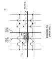
- FIG. 6Ais a plan view layout of a portion of the memory cell array of FIG. 4A illustrating word line segments of two memory cells which share a gate (for example, a gate comprised of polysilicon), according to certain aspects of the present inventions;
- a gatefor example, a gate comprised of polysilicon
- FIG. 6Bis schematic block diagram illustration of a portion of a memory cell array which corresponds to the layout of FIG. 6A , according to certain aspects of the present inventions;
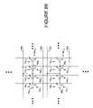
- FIG. 7Ais a plan view layout of a portion of the memory cell array of FIG. 4B illustrating word line segments of four memory cells which share a gate (for example, a gate comprised of polysilicon), according to certain aspects of the present inventions;
- a gatefor example, a gate comprised of polysilicon
- FIG. 7Bis schematic block diagram illustration of a portion of a memory cell array which corresponds to the layout of FIG. 7A , according to certain aspects of the present inventions;
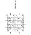
- FIG. 8Ais a plan view layout of a portion of the memory cell array illustrating word line segments of four memory cells which share a gate (for example, a gate comprised of a polysilicon material) with a central contact, according to certain aspects of the present inventions;
- a gatefor example, a gate comprised of a polysilicon material
- FIG. 8Bis schematic block diagram illustration of a portion of a memory cell array which corresponds to the layout of FIG. 8A , according to certain aspects of the present inventions;
- FIGS. 9A-9Care schematic representations of memory cell array(s), including a plurality of memory cells (for example, electrically body transistors or electrically floating gate transistors) in conjunction with data sense circuitry, according to various embodiments of the present inventions;
- FIGS. 10A and 10Bare schematic block diagram illustrations of two embodiments of the architecture of a portion of a memory cell array comprised of a plurality of memory cells, and associated data sense/write circuitry, in conjunction with certain peripheral circuitry (i.e., reference generator circuitry and memory cell selection circuitry), according certain aspects of the present inventions;
- peripheral circuitryi.e., reference generator circuitry and memory cell selection circuitry
- FIG. 11is a schematic block diagram illustration of another exemplary embodiment of the bit line selection circuit, in conjunction with data sense/write circuitry, and certain peripheral circuitry (i.e., reference generator circuitry and memory cell selection circuitry), according to certain aspects of the present inventions;
- FIG. 12is a schematic representation of one embodiment of one aspect of the circuitry and techniques for adjusting, setting, determining, controlling and/or generating a reference current, using a MOS transistor “ratioing” configuration, as described and illustrated in application Ser. No. 11/515,667 (U.S. Patent Application Publication US 2007/0064489), for one aspect of the data sense amplifier circuitry of the present inventions;
- FIG. 13is a schematic representation of one embodiment of one aspect of the circuitry and techniques for adjusting, setting, determining, controlling and/or generating a reference current, using the state of a control bit to a plurality of pair of reference cells in order to implement a digital control of the reference current level (employed during a read operation), as described and illustrated in application Ser. No. 11/515,667 (U.S. Patent Application Publication US 2007/0064489), for one aspect of the data sense amplifier circuitry of the present inventions; and
- FIGS. 14A-14Care schematic block diagram illustrations of exemplary integrated circuit devices in which the memory cell array (and certain peripheral circuitry) may be implemented, according to one or more aspects of the present inventions.
- the present inventionsare directed to an architecture, a configuration or a layout of a semiconductor memory cell array having a plurality of memory cells, arranged in a plurality of rows, and data sense and write circuitry to write data into and/or read data from such memory cells.
- the memory cell arraymay comprise a portion of an integrated circuit device, for example, a logic device (such as, a microcontroller or microprocessor) or a memory device (such as, a discrete memory).
- each memory cellincludes at least one electrically floating body transistor.
- an integrated circuit devicemay include data sense and write circuitry and certain peripheral circuitry to implement control, refresh, hold, read and/or write operations relative to a memory cell array having a plurality of memory cells.
- each memory cellincludes at least one electrically floating body transistor.
- integrated circuit device 100includes memory cell array 102 having a plurality of memory cells 12 , each including an electrically floating body transistor 14 .
- the memory cells 12are connected to word lines 28 (via the gate of transistor 14 ) and bit lines 32 (via the drain of transistor 14 ).
- two adjacent memory cells 12are interconnected to an associated word line 28 via an associated word line segment.
- the gates of adjacent transistors 14 a 1 and 14 a 2 of adjacent memory cells 12 a 1 and 12 a 2respectively, are connected to an associated word line 28 a via word line segment 28 a 1 .
- the gates of adjacent transistors 14 a 3 and 14 a 4 of adjacent memory cells 12 a 3 and 12 a 4 , respectively,are connected to an associated word line 28 b via word line segment 28 b 1 .
- the gates of adjacent transistors 14 z 1 and 14 z 2 of adjacent memory cells 12 z 1 and 12 z 2 , respectively,are connected to an associated word line 28 y via a word line segment 28 y 1 ; and the gates of adjacent transistors 14 z 3 and 14 z 4 of adjacent memory cells 12 z 3 and 12 z 4 , respectively, are connected to an associated word line 28 z via a word line segment 28 z 1 .
- the word line segmentsmay be formed from a polysilicon material.
- the drain regions of the adjacent transistors 14 of the adjacent memory cells 12are connected to adjacent bit lines 32 .
- the drain regions of adjacent transistors 14 a 1 and 14 a 2 of adjacent memory cells 12 a 1 and 12 a 2 , respectively,are connected to bit line 32 a and 32 b , respectively.
- the drain regions of adjacent transistors 14 a 3 and 14 a 4 of adjacent memory cells 12 a 3 and 12 a 4are connected to bit lines 32 c and 32 d , respectively.
- the drain regions of adjacent transistors 14 z 1 and 14 z 2 of adjacent memory cells 12 z 1 and 12 z 2are connected to bit lines 32 a and 32 b , respectively.
- the drain regions of adjacent transistors 14 z 3 and 14 z 4 of adjacent memory cells 12 z 3 and 12 z 4are connected to bit lines 32 c and 32 d , respectively.
- the integrated circuit device 100further includes memory cell selection circuitry 104 and reading and programming circuitry 106 .
- memory cell selection circuitry 104selects or enables one or more memory cells 12 to facilitate reading data therefrom and/or writing data thereto by applying a control signal on one or more word line 28 .
- memory cell selection circuitry 104may be a conventional word line decoder and/or driver.
- control/selection techniquesand circuitry therefor to implement the memory cell selection technique. Such techniques, and circuitry therefor, are well known to those skilled in the art. Notably, all such control/selection techniques, and circuitry therefor, whether now known or later developed, are intended to fall within the scope of the present inventions.
- reading and programming circuitry 106reads data from and writes data to selected memory cells 12 .
- the reading and programming circuitry 106include data sense/write circuitry 108 a - x .
- the data sense/write circuitry 108 a - xare coupled to receive an output of reference generator circuitry 110 (for example, a current or voltage reference) and are coupled to a plurality of associated bit lines 32 .
- reference generator circuitry 110for example, a current or voltage reference
- data sense/write circuitry 108 acouples to bit lines 32 a and 32 c
- data sense/write circuitry 108 bcouples to bit lines 32 b and 32 d .
- data sense/write circuitry 108 ccouples to bit lines 32 e and 32 g
- data sense/write circuitry 108 dcouples to bit lines 32 f and 32 h.
- data sense/write circuitry 108includes a data sense amplifier (for example, a cross-coupled sense amplifier as described and illustrated in the Non-Provisional U.S. patent application Ser. No. 11/299,590 (U.S. Patent Application Publication US 2006/0126374), filed by Waller and Carman, on Dec. 12, 2005 and entitled “Sense Amplifier Circuitry and Architecture to Write Data into and/or Read Data from Memory Cells”, the application being incorporated herein by reference in its entirety) to sense the data state stored in memory cell 12 and/or write-back data into memory cell 12 .
- the data sense amplifiermay employ voltage and/or current sensing circuitry and/or techniques.
- a current sense amplifiermay compare the current from the selected memory cell to a reference current, for example, the current of one or more reference cells. From that comparison, it may be determined whether memory cell 12 contained a logic high (relatively more majority carries 34 contained within body region 18 ) or logic low data state (relatively less majority carries 28 contained within body region 18 ).
- data sense/write circuitry 108is coupled to two bit lines.
- one of the bit linesi.e., the active bit line
- the active bit lineis selectively connected to the data sense and/or write circuitry in order to sense the data state in a memory cell and/or write a data state into a memory cell which is associated with the selected bit line.
- the active bit lineis selected by memory selection circuitry 104 using, for example, one or more bits of the row address (for example, the MSB or LSB).
- the other bit lineis disconnected from the sensing circuitry of data sense/write circuitry 108 .
- reading and programming circuitry 106includes bit line selection circuit 114 to select one of the bit lines connected to data sense/write circuitry 108 .
- bit line selection circuit 114may include two P-channel type transistors that receive either the control signal on signal line 112 a (from memory selection circuitry 104 ) or the control signal on signal line 112 b .
- one of two associated bit lines 32(for example, bit lines 32 a or 32 c , or bit lines 32 b or 32 d ) is connected to the appropriate circuitry in data sense/write circuitry 108 .
- any bit line selection circuitwhether now known or later developed is intended to fall within the scope of the present inventions.
- integrated circuit device 100also includes reference generator circuitry 110 .
- reference generator circuitry 110generates a reference (for example, a voltage and/or current reference) which is provided to reading and programming circuitry 106 via signal line 116 .
- the reading and programming circuitry 106and, in particular, data sense/write circuitry 108 employs the reference to determine the data state of the selected memory cell 12 during, for example, a read operation.
- memory cell selection circuitry 104in response to an address signal designating for example, a memory cell 12 connected to word line 28 b , applies a control signal on word line 28 b (and correspondingly word line segment 28 b 1 among other word line segments connected to word line 28 b including word line segment 28 b 2 ).
- memory cell selection circuitry 104applies a control signal on signal lines 112 which connects bit line 32 c to the data sensing circuitry in data sense/write circuitry 108 a , bit line 32 d to the data sensing circuitry in data sense/write circuitry 108 b , bit line 32 g to the data sensing circuitry in data sense/write circuitry 108 c , and bit line 32 h to the data sensing circuitry in data sense/write circuitry 108 d .
- the data sensing circuitry(for example, a cross-coupled sense amplifier) in data sense/write circuitry 108 a , 108 b , 108 c and 108 d sample, sense, read and/or determine the data state stored in memory cells 12 a 3 , 12 a 4 , 12 a 7 , and 12 a 8 , respectively.
- the data sensing circuitry in data sense/write circuitry 108compares a signal from the selected memory cells 12 (in this example, memory cells 12 a 3 , 12 a 4 , 12 a 7 , and 12 a 8 ) to one or more references from reference generator circuitry 110 to determine the data state stored in the selected memory cells 12 .
- memory cell selection circuitry 104applies a control signal on word line 28 b as well as a control signal on signal lines 112 which connects bit line 32 c to the data writing circuitry in data sense/write circuitry 108 a , bit line 32 d to the data writing circuitry in data sense/write circuitry 108 b , bit line 32 g to the data writing circuitry in data sense/write circuitry 108 c , and bit line 32 h to the data writing circuitry in data sense/write circuitry 108 d .
- memory cells 12 a 3 , 12 a 4 , 12 a 7 , and 12 a 8are connected to the data writing circuitry of data sense/write circuitry 108 a , 108 b , 108 c , and 108 d , respectively.
- the data writing circuitry in data sense/write circuitry 108 a , 108 b , 108 c and 108 dwrites and/or programs a data state in memory cells 12 a 3 , 12 a 4 , 12 a 7 , and 12 a 8 , respectively.
- memory cell selection circuitry 104applies a control signal on signal lines 112 which connects bit line 32 a to the data sensing circuitry in data sense/write circuitry 108 a , bit line 32 b to the data sensing circuitry in data sense/write circuitry 108 b , bit line 32 e to the data sensing circuitry in data sense/write circuitry 108 c , and bit line 32 f to the data sensing circuitry in data sense/write circuitry 108 d .
- the data sensing circuitry and/or data writing circuitry in data sense/write circuitry 108 a , 108 b , 108 c and 108 dperforms the appropriate operation (for example, read operation) with respect to memory cells 12 a 1 , 12 a 2 , 12 a 5 , and 12 a 6 , respectively.
- the present inventionsmay include memory cells 12 having electrically floating body transistor 14 , as described above.
- electrically floating body transistor 14is an N-channel type transistor.
- the word line segments 28interconnect and form the gates of adjacent transistors of adjacent memory cells.
- word line segment 28 a xforms the gate of transistor 14 a x (of memory cell 12 a x ) and 14 a x+1 (of memory cell 12 a x+1 ).
- word line segment 28 b xforms the gate of transistor 14 a x+2 (of memory cell 12 a x+2 ) and 14 a x+3 (of memory cell 12 a x+3 ).
- word line segment 28 c xforms the gate of transistor 14 c x (of memory cell 12 c x ) and 14 c x+1 (of memory cell 12 c x+1 ).
- word line segment 28 c x+2forms the gate of transistor 14 c x+2 (of memory cell 12 c x ) and 14 c x+3 (of memory cell 12 c x+3 ).
- the configuration and/or layout of the memory cells 12is proportional and/or equal to the pitch of the data sensing circuitry (for example, a data sense amplifier) in data sense/write circuitry 108 .
- word line segmentsare employed to interconnect more than two adjacent transistors of adjacent memory cells.
- word line segment 28 a 1interconnects gates of transistors 14 a 1 , 14 a 2 , 14 a 3 , and 14 a 4 of memory cells 12 a 1 , 12 a 2 , 12 a 3 , and 12 a 4 , respectively.
- word line segment 28 b 1interconnects gates of transistors 14 a 5 , 14 a 6 , 14 a 7 , and 14 a 8 of memory cells 12 a 5 , 12 a 6 , 12 a 7 , and 12 a 8 , respectively.
- word line segment 28 y 1interconnects gates of transistors 14 z 1 , 14 z 2 , 14 z 3 , and 14 z 4 of memory cells 12 z 1 , 12 z 2 , 12 z 3 , and 12 z 4 , respectively; and word line segment 28 z 1 interconnects gates of transistors 14 z 5 , 14 z 6 , 14 z 7 , and 14 z 8 of memory cells 12 z 5 , 12 z 6 , 12 z 7 , and 12 z 8 , respectively.
- the configuration and/or layout of the memory cells 12is proportional and/or equal to the pitch of the data sensing circuitry (for example, a data sense amplifier) in data sense/write circuitry 108 .
- bit lines 32 c and 32 dare routed “outside” the pitch of the data sensing circuitry to connect, for example, memory cell 12 a 3 and 12 a 4 to the data sensing circuitry of data sense/write circuitry 108 c and 108 d , respectively.
- memory cell selection circuitry 104applies a control signal on signal lines 112 which connects bit line 32 a to the data sensing circuitry in data sense/write circuitry 108 a , bit line 32 b to the data sensing circuitry in data sense/write circuitry 108 b , bit line 32 c to the data sensing circuitry in data sense/write circuitry 108 c , and bit line 32 d to the data sensing circuitry in data sense/write circuitry 108 d .
- the data sensing circuitry and/or data writing circuitry in data sense/write circuitry 108 a , 108 b , 108 c and 108 dperforms the appropriate operation (for example, read or write operation) with respect to memory cells 12 a 1 , 12 a 2 , 12 a 3 , and 12 a 4 , respectively.
- the present inventionsmay include memory cells 12 having electrically floating body transistor 14 , as described above.
- electrically floating body transistor 14is an N-channel type transistor.
- the word line segments 28interconnect and form the gates of adjacent transistors of adjacent memory cells.
- word line segment 28 a xforms the gate of transistor 14 a x (of memory cell 12 a x ), the gate of transistor 14 a x+1 (of memory cell 12 a x+1 ), the gate of transistor 14 a x+2 (of memory cell 12 a x+2 ) and the gate of transistor 14 a x+3 (of memory cell 12 a x+3 ).
- word line segment 28 c xforms the gate of transistor 14 c x (of memory cell 12 c x ), the gate of transistor 14 c x+1 (of memory cell 12 c x+1 ), the gate of transistor 14 c x+2 (of memory cell 12 c x ) and the gate of transistor 14 c x+3 (of memory cell 12 c x+3 ).
- the configuration and/or layout of the memory cells 12is proportional and/or equal to the pitch of the data sensing circuitry (for example, a data sense amplifier) in data sense/write circuitry 108 . In one embodiment (referring again to FIG.
- the memory architectures of FIGS. 4A and 4Binclude a layout whereby each data sense/write circuitry 108 is associated with two bit lines 32 and, as such, performs the appropriate operation (for example, read operation relative to the reference) with respect to memory cells 12 connected to the associated two bit lines.
- the number of data sense/write circuitry for a given memory array sizeis reduced.
- this configurationfacilitates a more compact, lower power consumption architecture because fewer data sense/write circuitry 108 are employed relative to a given memory array size.
- the configuration illustrated in FIG. 4Bmay be more dense than the configuration of FIG. 4A due to increased density of the memory array. In this regard, there are fewer “spaces” between and contacts to the word line segments. As such, transistors 14 of memory cells 12 may be located or placed closer.
- FIGS. 4A , 4 B, 6 A, 6 B, 7 A and 7 Bare merely exemplary.
- the contacts to word line segments 28are located in the “center” of the associated memory cells 12 .
- FIGS. 7A and 7Bthe bit line associated with memory cells 12 a x and 12 c x and the bit line associated with memory cells 12 a x+3 and 12 c x+3 may be routed to an associated data sensing circuitry of data sense/write circuitry 108 .
- bit line associated with memory cells 12 a x+1 and 12 c x+1 and the bit line associated with memory cells 12 a x+2 and 12 c x+2may be routed to an associated data sensing circuitry of data sense/write circuitry 108 .
- all layouts and configurationsare intended to fall within the scope of the present inventions.
- the present inventionsmay be implemented in any electrically floating body memory cell and memory cell array.
- the present inventionsare directed to a memory array, having a plurality of memory cells each including an electrically floating body transistor, and/or technique of writing or programming data into one or more memory cells of such a memory array.
- the data states of adjacent memory cells and/or memory cells that share a word linemay be individually programmed.
- the memory cells of the memory cell arraymay be comprised of N-channel, P-channel and/or both types of transistors.
- circuitry that is peripheral to the memory arrayfor example, sense amplifiers or comparators, row and column address decoders, as well as line drivers (not illustrated herein) may include N-channel type and/or P-channel type transistors.
- suitable write and read voltagesfor example, negative voltages are well known to those skilled in the art in light of this disclosure as well as applications incorporated by reference.
- integrated circuit device 100may include a plurality of memory cell arrays 102 a - x , each having corresponding reading and programming circuitry 106 a - x .
- integrated circuit device 100may include memory array 102 which is connected to reading and programming circuitry 106 a and 106 b .
- memory array 102is embedded memory within an integrated circuit device 100 which includes extensive logic circuitry (not illustrated).
- integrated circuit 100may include a plurality of arrays 102 a - 102 d , connected to reading and programming circuitry 106 a - 106 f , respectively.
- the reading and programming circuitry 106 a - 106 fmay be located or disposed at the edges and in the center of the associated arrays 102 a - 102 d , respectively. (See, for example, FIG. 9C ).
- memory arrays 102 a - 102 dshare reading and programming circuitry 106 c and 106 d.
- the pitch of the sensing/writing circuitry (for example, sense amplifier circuitry) in data sense/write circuitry 108corresponds to, or substantially corresponds to, the pitch of “nx2” memory cells—wherein “n” is equal to the number of groups of word line segments for each row of cells.
- the exemplary embodimentsuse a value of two such that the pitch of the data sense/write circuitry 108 is four.
- the factor of 2 in the equationrepresents the fact that there are data sense/write circuits on two sides of the array. Further, this determines the pitch of the data sense/write circuitry such that a single bank of data sense/write circuitry can be placed on either side of the memory array.
- Such an architecture or configurationfacilitates sharing of data sense/write circuitry 108 of reading and programming circuitry 106 by “adjacent” arrays (see, for example, FIG. 9A wherein memory arrays 102 a and 102 b share the sense/write circuitry of reading and programming circuitry 106 b ).
- the present inventionsmay be employed or implemented in conjunction with one or more of the inventions, memory cells, memory arrays, and techniques for programming, reading, controlling and/or operating a memory cell and array of the following provisional U.S. patent applications:
- the memory cellsmay be arranged, configured and/or controlled using any of the memory cell arrays, architectures and/or control/operation techniques.
- the memory cellsmay be arranged, configured and/or controlled using any of the memory cell arrays, architectures and/or control/operation techniques described and illustrated in the following provisional and non-provisional U.S. patent applications:
- the present inventionsmay be implemented in conjunction with memory cells 118 which implement any memory cell technology that generates at least two current or voltage values (each current or voltage being representative of, for example, a respective data state) and employs a reference to discriminate such data states.
- the memory cells 118may be comprised of electrically floating gate transistors, junction field effect transistors (often referred to as JFETs), or any other memory/transistor technology whether now known (for example, one transistor one capacitor) or later developed. All such memory technologies are considered to fall within the scope of the present inventions.
- memory cells 118may be employed in any of the embodiments described and/or illustrated herein. Indeed, all permutations and combinations of the memory cells with such embodiments and/or features thereof, are intended to come within the scope of the present inventions. For the sake of brevity, such permutations and combinations are not discussed in detail herein.
- electrically floating body transistor 14may be a symmetrical or non-symmetrical device. Where transistor 14 is symmetrical, the source and drain regions are essentially interchangeable. However, where transistor 14 is a non-symmetrical device, the source or drain regions of transistor 14 have different electrical, physical, doping concentration and/or doping profile characteristics. As such, the source or drain regions of a non-symmetrical device are typically not interchangeable. This notwithstanding, the drain region of the electrically floating N-channel type transistor of the memory cell (whether the source and drain regions are interchangeable or not) is that region of the transistor that is connected to the bit line/sense amplifier.
- the inventionsare entirely applicable to N-channel and/or P-channel type transistors.
- the discussion described and illustratedonly source and drain implants, other implants may also be included.
- implants to modify the operation of memory cells 12which affect, for example, the power consumption of memory cells 12 as described and illustrated in (1) U.S. Pat. No. 6,969,662 (identified above), (2) U.S. Pat. No. 7,061,050 (identified above), and (3) Provisional Application Ser. No. 60/578,631, which was filed on Jun. 10, 2004 and entitled “Asymmetrical Electrically Floating Body Memory Device, and Method of Manufacturing Same”.
- the memory arraysmay be comprised of N-channel type transistors, P-channel type transistors and/or both types of transistors, as well as partially depleted and/or fully depleted type transistors.
- circuitry that is peripheral to the memory arraymay include fully depleted type transistors (whether P-channel and/or N-channel type).
- circuitrymay include partially depleted type transistors (whether P-channel and/or N-channel type).
- memory cell selection circuitry 104may employ any circuitry and/or technique now known or later developed to select one or more memory cells for reading and/or programming. Indeed, all such techniques and circuitry therefor, whether now known or later developed, are intended to fall within the scope of the present inventions.
- reading and programming circuitry 106may employ any bit line selection circuit whether now known or later developed.
- bit line selection circuit 114may employ a CMOS pass gate configuration wherein each bit line is connected to an input of data sense/write circuitry 108 via a CMOS pass gate configuration.
- bit line selection circuit 114may include N-channel type transistors which receive control signals (from memory selection circuitry 104 ) on signal lines 112 a and 112 b , respectively.
- one of the two bit lines 32(for example, bit lines 32 a and 32 c ) is connected to the appropriate circuitry in data sense/write circuitry 108 .
- any bit line selection circuitwhether now known or later developed is intended to fall within the scope of the present inventions.
- bit line selection circuitmay eliminate, reduce and/or minimize bit line disturbance as well as reduce bit line capacitance from the perspective of data sense/write circuitry 108 .
- bit line selection circuit 114may include “protection” circuitry or transistors in order to facilitate implementation of transistors having relatively thin gate oxides in bit line selection circuit 114 notwithstanding relatively high voltages applied on/to the bit lines during, for example, a write operation.
- the reading and programming circuitry 106may include output pass gates, latches and/or column switch circuitry to facilitate and/or implement read and write operations to memory cells 12 .
- output pass gateslatches and/or column switch circuitry to facilitate and/or implement read and write operations to memory cells 12 .
- circuitryThere are many different configurations and techniques (and circuitry therefor) to implement such circuitry. All such configurations and techniques, whether now known or later developed, are intended to fall within the scope of the present inventions.
- data sense/write circuitry 108may employ a sense amplifier to read the data stored in memory cells 12 .
- the sense amplifiermay sense the data state stored in memory cell 12 using voltage or current sensing techniques.
- a current sense amplifierfor example, Non-Provisional U.S. patent application Ser. No. 11/299,590 (U.S. Patent Application Publication US 2006/0126374), filed by Waller and Carman, on Dec. 12, 2005 and entitled “Sense Amplifier Circuitry and Architecture to Write Data into and/or Read Data from Memory Cells”, the sense amplifier may compare the memory cell current to a reference current, for example, the current of a reference cell.
- the data state of memory cell 12may be determined (for example, whether the memory cell 12 contained a logic high (relatively more majority carries 34 contained within body region 18 ) or logic low data state (relatively less majority carries 28 contained within body region 18 )).
- the reference current or voltagemay be substantially equal to one-half of the summation of the currents in a first reference cell, which has a logic low data state, and a second reference cell, which has a logic high data state. Other reference current or voltage levels are suitable.
- reference generator circuitry 110is described in the context of generating, providing and/or supplying a reference current or voltage.
- the circuitry and techniques described and illustrated in U.S. patent application Ser. No. 10/840,902which was filed by Portmann et al. on May 7, 2004, and entitled “Reference Current Generator, and Method of Programming, Adjusting and/or Operating Same” (now U.S. Pat. No. 6,912,150), may be employed to generate an appropriate reference current for data sense/write circuitry 108 .
- the entire contents of U.S. patent application Ser. No. 10/840,902including, for example, the inventions, features, attributes, architectures, configurations, materials, techniques and advantages described and illustrated therein, are hereby incorporated by reference herein.
- the present inventionsmay employ the circuitry and techniques for independently controlling certain parameters (for example, temporal or voltage), for a memory operation (for example, restore, write, refresh), to program or write a predetermined data state into a memory cell (for example, programming or writing data state “1” or “0” into a memory cell) as described and illustrated in U.S. patent application Ser. No. 11/590,147, which was filed by Popov et al. on Oct. 31, 2006, and entitled “Method and Apparatus for Varying the Programming Duration and/or Voltage of an Electrically Floating Body Transistor, and Memory Cell Array Implementing Same”.
- certain parametersfor example, temporal or voltage
- a memory operationfor example, restore, write, refresh
- program or write a predetermined data state into a memory cellfor example, programming or writing data state “1” or “0” into a memory cell
- the duration of programming/writing/refreshing of a given memory state into a memory cell by data sense/write circuitry 108may be controlled, adjusted, determined and/or predetermined according to or based on the given memory operation (for example, restore, write, refresh).
- the voltage conditions applied to the memory cell for programming/writing a given memory state into a memory cell by data sense/write circuitry 108may be controlled and/or adjusted according to the memory operation (for example, restore, write, refresh).
- the electrically floating memory cells, transistors and/or memory array(s)may be fabricated using well known techniques and/or materials. Indeed, any fabrication technique and/or material, whether now known or later developed, may be employed to fabricate the electrically floating body memory cells, transistors and/or memory array(s).
- the present inventionsmay employ silicon (whether bulk-type or SOI), germanium, silicon/germanium, gallium arsenide or any other semiconductor material in which transistors may be formed.
- the electrically floating transistors, memory cells, and/or memory array(s)may employ the techniques described and illustrated in non-provisional patent application entitled “Integrated Circuit Device, and Method of Fabricating Same”, which was filed on Jul. 2, 2004, by Fazan, Ser. No.
- memory array 102may be integrated with SOI logic transistors, as described and illustrated in the Integrated Circuit Device Patent Applications.
- an integrated circuit deviceincludes memory section (having, for example, PD or FD SOI memory transistors 14 ) and logic section (having, for example, high performance transistors, such as FinFET, multiple gate transistors, and/or non-high performance transistors (for example, single gate transistors that do not possess the performance characteristics of high performance transistors—not illustrated)).
- memory sectionhaving, for example, PD or FD SOI memory transistors 14
- logic sectionhaving, for example, high performance transistors, such as FinFET, multiple gate transistors, and/or non-high performance transistors (for example, single gate transistors that do not possess the performance characteristics of high performance transistors—not illustrated)).
- the memory cell and/or memory cell array, as well as the circuitry of the present inventionsmay be implemented in an integrated circuit device having a memory portion and a logic portion (see, for example, FIGS. 14A and 14C ), or an integrated circuit device that is primarily a memory device (see, for example, FIG. 14B ).
- the memory arraymay include a plurality of memory cells arranged in a plurality of rows and columns wherein each memory cell includes an electrically floating body transistor.
- the memory arraysmay be comprised of N-channel, P-channel and/or both types of transistors.
- circuitry that is peripheral to the memory arraymay include P-channel and/or N-channel type transistors.
- the memory arraysmay be comprised of N-channel, P-channel and/or both types of transistors, as well as partially depleted and/or fully depleted type transistors.
- circuitry that is peripheral to the memory arraymay include fully depleted type transistors (whether P-channel and/or N-channel type).
- circuitrymay include partially depleted type transistors (whether P-channel and/or N-channel type).
- electrically floating body transistor 14may be a symmetrical or non-symmetrical device. Where transistor 14 is symmetrical, the source and drain regions are essentially interchangeable. However, where transistor 14 is a non-symmetrical device, the source or drain regions of transistor 14 have different electrical, physical, doping concentration and/or doping profile characteristics. As such, the source or drain regions of a non-symmetrical device are typically not interchangeable. This notwithstanding, the drain region of the electrically floating N-channel transistor of the memory cell (whether the source and drain regions are interchangeable or not) is that region of the transistor that is connected to the bit line/sense amplifier.
- circuitmeans, among other things, a single component or a multiplicity of components (whether in integrated circuit form or otherwise), which are active and/or passive, and which are coupled together to provide or perform a desired operation.
- circuitrymeans, among other things, a circuit (whether integrated or otherwise), or a group of circuits (whether integrated or otherwise).
- to sense a/the data state stored in memory cellmeans, among other things, to sample, to sense, to read and/or to determine a/the data state stored in memory cell; “sensing a/the data state stored in memory cell”, “sensed a/the data state stored in memory cell” or the like shall have the same meaning.
Landscapes
- Semiconductor Memories (AREA)
- Dram (AREA)
Abstract
Description
Claims (28)
Priority Applications (1)
| Application Number | Priority Date | Filing Date | Title |
|---|---|---|---|
| US11/787,718US7606098B2 (en) | 2006-04-18 | 2007-04-17 | Semiconductor memory array architecture with grouped memory cells, and method of controlling same |
Applications Claiming Priority (2)
| Application Number | Priority Date | Filing Date | Title |
|---|---|---|---|
| US79282006P | 2006-04-18 | 2006-04-18 | |
| US11/787,718US7606098B2 (en) | 2006-04-18 | 2007-04-17 | Semiconductor memory array architecture with grouped memory cells, and method of controlling same |
Publications (2)
| Publication Number | Publication Date |
|---|---|
| US20070241405A1 US20070241405A1 (en) | 2007-10-18 |
| US7606098B2true US7606098B2 (en) | 2009-10-20 |
Family
ID=38604048
Family Applications (1)
| Application Number | Title | Priority Date | Filing Date |
|---|---|---|---|
| US11/787,718Active2028-02-17US7606098B2 (en) | 2006-04-18 | 2007-04-17 | Semiconductor memory array architecture with grouped memory cells, and method of controlling same |
Country Status (1)
| Country | Link |
|---|---|
| US (1) | US7606098B2 (en) |
Cited By (2)
| Publication number | Priority date | Publication date | Assignee | Title |
|---|---|---|---|---|
| US20100020622A1 (en)* | 2007-07-04 | 2010-01-28 | Hee Bok Kang | One-transistor type dram |
| US20150357047A1 (en)* | 2014-06-05 | 2015-12-10 | Micron Technology, Inc. | Comparison operations in memory |
Families Citing this family (7)
| Publication number | Priority date | Publication date | Assignee | Title |
|---|---|---|---|---|
| US7630262B2 (en)* | 2007-07-04 | 2009-12-08 | Hynix Semiconductor, Inc. | One-transistor type dram |
| KR101195268B1 (en)* | 2011-02-14 | 2012-11-14 | 에스케이하이닉스 주식회사 | Semiconductor device comprising capacitor and double-layered metal contact and method for fabricating the same |
| US9892767B2 (en) | 2016-02-12 | 2018-02-13 | Micron Technology, Inc. | Data gathering in memory |
| US9899070B2 (en) | 2016-02-19 | 2018-02-20 | Micron Technology, Inc. | Modified decode for corner turn |
| US9659605B1 (en) | 2016-04-20 | 2017-05-23 | Micron Technology, Inc. | Apparatuses and methods for performing corner turn operations using sensing circuitry |
| US10153008B2 (en)* | 2016-04-20 | 2018-12-11 | Micron Technology, Inc. | Apparatuses and methods for performing corner turn operations using sensing circuitry |
| US12069846B2 (en)* | 2019-01-29 | 2024-08-20 | Semiconductor Energy Laboratory Co., Ltd. | Memory device |
Citations (195)
| Publication number | Priority date | Publication date | Assignee | Title |
|---|---|---|---|---|
| US3439214A (en) | 1968-03-04 | 1969-04-15 | Fairchild Camera Instr Co | Beam-junction scan converter |
| FR2197494A5 (en) | 1972-08-25 | 1974-03-22 | Radiotechnique Compelec | |
| GB1414228A (en) | 1972-04-25 | 1975-11-19 | Ibm | Semiconductor storage devices |
| US3997799A (en) | 1975-09-15 | 1976-12-14 | Baker Roger T | Semiconductor-device for the storage of binary data |
| US4032947A (en) | 1971-10-20 | 1977-06-28 | Siemens Aktiengesellschaft | Controllable charge-coupled semiconductor device |
| US4250569A (en) | 1978-11-15 | 1981-02-10 | Fujitsu Limited | Semiconductor memory device |
| US4262340A (en) | 1978-11-14 | 1981-04-14 | Fujitsu Limited | Semiconductor memory device |
| US4298962A (en) | 1979-01-25 | 1981-11-03 | Nippon Electric Co., Ltd. | Memory |
| US4371955A (en) | 1979-02-22 | 1983-02-01 | Fujitsu Limited | Charge-pumping MOS FET memory device |
| EP0030856B1 (en) | 1979-12-13 | 1984-03-21 | Fujitsu Limited | Charge-pumping semiconductor memory cell comprising a charge-storage region and memory device using such a cell |
| US4527181A (en) | 1980-08-28 | 1985-07-02 | Fujitsu Limited | High density semiconductor memory array and method of making same |
| US4630089A (en) | 1983-09-27 | 1986-12-16 | Fujitsu Limited | Semiconductor memory device |
| JPS62272561A (en) | 1986-05-20 | 1987-11-26 | Seiko Epson Corp | 1 transistor memory cell |
| US4791610A (en) | 1985-05-24 | 1988-12-13 | Fujitsu Limited | Semiconductor memory device formed of a SOI-type transistor and a capacitor |
| EP0354348A2 (en) | 1988-08-10 | 1990-02-14 | International Business Machines Corporation | CMOS-transistor and one-capacitor dram cell and fabrication process therefor |
| US4954989A (en) | 1988-04-12 | 1990-09-04 | Commissariat A L'energie Atomique | MIS type static memory cell and memory and storage process |
| JPH02294076A (en) | 1989-05-08 | 1990-12-05 | Hitachi Ltd | Semiconductor integrated circuit device |
| US4979014A (en) | 1987-08-10 | 1990-12-18 | Kabushiki Kaisha Toshiba | MOS transistor |
| EP0202515B1 (en) | 1982-11-04 | 1991-03-13 | Hitachi, Ltd. | Semiconductor memory |
| JPH03171768A (en) | 1989-11-30 | 1991-07-25 | Toshiba Corp | semiconductor storage device |
| EP0175378B1 (en) | 1984-09-21 | 1991-11-21 | Fujitsu Limited | Dynamic random access memory (dram) |
| EP0253631B1 (en) | 1986-07-14 | 1992-04-22 | Oki Electric Industry Company, Limited | Semiconductor memory device |
| US5144390A (en) | 1988-09-02 | 1992-09-01 | Texas Instruments Incorporated | Silicon-on insulator transistor with internal body node to source node connection |
| US5164805A (en) | 1988-08-22 | 1992-11-17 | Massachusetts Institute Of Technology | Near-intrinsic thin-film SOI FETS |
| EP0300157B1 (en) | 1987-07-20 | 1993-05-05 | International Business Machines Corporation | Vertical transistor capacitor memory cell structure and fabrication method therefor |
| US5258635A (en) | 1988-09-06 | 1993-11-02 | Kabushiki Kaisha Toshiba | MOS-type semiconductor integrated circuit device |
| EP0350057B1 (en) | 1988-07-07 | 1993-12-01 | Kabushiki Kaisha Toshiba | Semiconductor memory |
| EP0362961B1 (en) | 1988-10-03 | 1994-02-16 | Interuniversitair Microelektronica Centrum Vzw | A method of operating a MOS-structure and MOS-structure therefor |
| EP0599506A1 (en) | 1992-11-27 | 1994-06-01 | International Business Machines Corporation | Semiconductor memory cell with SOI MOSFET |
| EP0564204A3 (en) | 1992-03-30 | 1994-09-28 | Mitsubishi Electric Corp | Semiconductor device |
| EP0359551B1 (en) | 1988-09-14 | 1994-12-28 | Kawasaki Steel Corporation | Semicoductor memory circuit |
| US5388068A (en) | 1990-05-02 | 1995-02-07 | Microelectronics & Computer Technology Corp. | Superconductor-semiconductor hybrid memory circuits with superconducting three-terminal switching devices |
| EP0366882B1 (en) | 1988-10-31 | 1995-05-24 | International Business Machines Corporation | An ultra dense DRAM cell array and its method of fabrication |
| EP0465961B1 (en) | 1990-07-09 | 1995-08-09 | Sony Corporation | Semiconductor device on a dielectric isolated substrate |
| EP0579566A3 (en) | 1992-06-17 | 1995-08-09 | Ibm | High-density dram structure on SOI. |
| US5446299A (en) | 1994-04-29 | 1995-08-29 | International Business Machines Corporation | Semiconductor random access memory cell on silicon-on-insulator with dual control gates |
| US5448513A (en) | 1993-12-02 | 1995-09-05 | Regents Of The University Of California | Capacitorless DRAM device on silicon-on-insulator substrate |
| EP0513923B1 (en) | 1991-05-15 | 1995-09-27 | Koninklijke Philips Electronics N.V. | Protected programmable transistor with reduced parasitic capacitances and method of fabrication |
| US5489792A (en) | 1994-04-07 | 1996-02-06 | Regents Of The University Of California | Silicon-on-insulator transistors having improved current characteristics and reduced electrostatic discharge susceptibility |
| US5506436A (en) | 1992-12-10 | 1996-04-09 | Sony Corporation | Semiconductor memory cell |
| EP0333426B1 (en) | 1988-03-15 | 1996-07-10 | Kabushiki Kaisha Toshiba | Dynamic RAM |
| JPH08213624A (en) | 1995-02-08 | 1996-08-20 | Fujitsu Ltd | Semiconductor memory device and operating method thereof |
| JPH08274277A (en) | 1995-03-31 | 1996-10-18 | Toyota Central Res & Dev Lab Inc | Semiconductor memory device and manufacturing method thereof |
| US5568356A (en) | 1995-04-18 | 1996-10-22 | Hughes Aircraft Company | Stacked module assembly including electrically interconnected switching module and plural electronic modules |
| EP0694977A3 (en) | 1994-07-14 | 1996-11-06 | Nec Corp | SOI-type semiconductor device with suppression of extension of the depletion region |
| US5593912A (en) | 1994-10-06 | 1997-01-14 | International Business Machines Corporation | SOI trench DRAM cell for 256 MB DRAM and beyond |
| JPH0946688A (en) | 1995-07-26 | 1997-02-14 | Fujitsu Ltd | Video information provision / reception system |
| US5606188A (en) | 1995-04-26 | 1997-02-25 | International Business Machines Corporation | Fabrication process and structure for a contacted-body silicon-on-insulator dynamic random access memory |
| US5608250A (en) | 1993-11-29 | 1997-03-04 | Sgs-Thomson Microelectronics S.A. | Volatile memory cell with interface charge traps |
| JPH0982912A (en) | 1995-09-13 | 1997-03-28 | Toshiba Corp | Semiconductor memory device and manufacturing method thereof |
| EP0245515B1 (en) | 1985-11-20 | 1997-04-16 | Hitachi, Ltd. | Semiconductor device |
| US5627092A (en) | 1994-09-26 | 1997-05-06 | Siemens Aktiengesellschaft | Deep trench dram process on SOI for low leakage DRAM cell |
| US5631186A (en) | 1992-12-30 | 1997-05-20 | Samsung Electronics Co., Ltd. | Method for making a dynamic random access memory using silicon-on-insulator techniques |
| US5696718A (en) | 1994-11-10 | 1997-12-09 | Commissariat A L'energie Atomique | Device having an electrically erasable non-volatile memory and process for producing such a device |
| EP0510607B1 (en) | 1991-04-23 | 1998-02-04 | Canon Kabushiki Kaisha | Semiconductor memory device |
| US5740099A (en) | 1995-02-07 | 1998-04-14 | Nec Corporation | Semiconductor memory device having peripheral circuit and interface circuit fabricated on bulk region out of silicon-on-insulator region for memory cells |
| US5778243A (en) | 1996-07-03 | 1998-07-07 | International Business Machines Corporation | Multi-threaded cell for a memory |
| US5780906A (en) | 1995-06-21 | 1998-07-14 | Micron Technology, Inc. | Static memory cell and method of manufacturing a static memory cell |
| US5784311A (en) | 1997-06-13 | 1998-07-21 | International Business Machines Corporation | Two-device memory cell on SOI for merged logic and memory applications |
| EP0537677B1 (en) | 1991-10-16 | 1998-08-19 | Sony Corporation | Method of forming an SOI structure with a DRAM |
| EP0860878A2 (en) | 1997-02-20 | 1998-08-26 | Texas Instruments Incorporated | An integrated circuit with programmable elements |
| JPH10242470A (en) | 1997-02-28 | 1998-09-11 | Toshiba Corp | Semiconductor device and manufacturing method thereof |
| US5811283A (en) | 1996-08-13 | 1998-09-22 | United Microelectronics Corporation | Silicon on insulator (SOI) dram cell structure and process |
| US5847411A (en) | 1996-04-11 | 1998-12-08 | Matsushita Electric Industrial Co., Ltd. | Semiconductor device having a channel region including a vacancy-introduced polysilicon layer |
| US5877978A (en) | 1996-03-04 | 1999-03-02 | Mitsubishi Denki Kabushiki Kaisha | Semiconductor memory device |
| US5886376A (en) | 1996-07-01 | 1999-03-23 | International Business Machines Corporation | EEPROM having coplanar on-insulator FET and control gate |
| US5886385A (en) | 1996-08-22 | 1999-03-23 | Kabushiki Kaisha Toshiba | Semiconductor device and manufacturing method thereof |
| JPH1187649A (en) | 1997-09-04 | 1999-03-30 | Hitachi Ltd | Semiconductor storage device |
| US5897351A (en) | 1997-02-20 | 1999-04-27 | Micron Technology, Inc. | Method for forming merged transistor structure for gain memory cell |
| EP0642173B1 (en) | 1993-08-19 | 1999-07-14 | Hitachi, Ltd. | Semiconductor element and semiconductor memory device using the same |
| EP0878804A3 (en) | 1997-05-15 | 1999-07-14 | STMicroelectronics, Inc. | Multiple transistor dynamic random access memory array architecture with simultaneous refresh of multiple memory cells during a read operation |
| US5930648A (en) | 1996-12-30 | 1999-07-27 | Hyundai Electronics Industries Co., Ltd. | Semiconductor memory device having different substrate thickness between memory cell area and peripheral area and manufacturing method thereof |
| US5929479A (en) | 1996-10-21 | 1999-07-27 | Nec Corporation | Floating gate type non-volatile semiconductor memory for storing multi-value information |
| US5936265A (en) | 1996-03-25 | 1999-08-10 | Kabushiki Kaisha Toshiba | Semiconductor device including a tunnel effect element |
| EP0727822B1 (en) | 1995-02-14 | 1999-08-11 | Canon Kabushiki Kaisha | Semiconductor memory device |
| US5943581A (en) | 1997-11-05 | 1999-08-24 | Vanguard International Semiconductor Corporation | Method of fabricating a buried reservoir capacitor structure for high-density dynamic random access memory (DRAM) circuits |
| US5943258A (en) | 1997-12-24 | 1999-08-24 | Texas Instruments Incorporated | Memory with storage cells having SOI drive and access transistors with tied floating body connections |
| US5977578A (en) | 1995-12-06 | 1999-11-02 | Micron Technology, Inc. | Method of forming dynamic random access memory circuitry and dynamic random access memory |
| US6018172A (en) | 1994-09-26 | 2000-01-25 | Mitsubishi Denki Kabushiki Kaisha | Semiconductor memory device including memory cell transistors formed on SOI substrate and having fixed body regions |
| US6097056A (en) | 1998-04-28 | 2000-08-01 | International Business Machines Corporation | Field effect transistor having a floating gate |
| US6096598A (en) | 1998-10-29 | 2000-08-01 | International Business Machines Corporation | Method for forming pillar memory cells and device formed thereby |
| EP0689252B1 (en) | 1990-03-20 | 2000-08-02 | Nec Corporation | Semiconductor device |
| EP0599388B1 (en) | 1992-11-20 | 2000-08-02 | Koninklijke Philips Electronics N.V. | Semiconductor device provided with a programmable element |
| US6111778A (en) | 1999-05-10 | 2000-08-29 | International Business Machines Corporation | Body contacted dynamic memory |
| EP0682370B1 (en) | 1994-05-13 | 2000-09-06 | Canon Kabushiki Kaisha | Storage device |
| EP0951072A4 (en) | 1996-04-08 | 2000-09-13 | Hitachi Ltd | SEMICONDUCTOR INTEGRATED CIRCUIT DEVICE |
| US6157216A (en) | 1999-04-22 | 2000-12-05 | International Business Machines Corporation | Circuit driver on SOI for merged logic and memory circuits |
| US6171923B1 (en) | 1997-11-20 | 2001-01-09 | Vanguard International Semiconductor Corporation | Method for fabricating a DRAM cell structure on an SOI wafer incorporating a two dimensional trench capacitor |
| US6177708B1 (en) | 1998-08-07 | 2001-01-23 | International Business Machines Corporation | SOI FET body contact structure |
| EP1073121A2 (en) | 1999-07-29 | 2001-01-31 | Fujitsu Limited | Semiconductor memory device and method for manufacturing the same |
| US6214694B1 (en) | 1998-11-17 | 2001-04-10 | International Business Machines Corporation | Process of making densely patterned silicon-on-insulator (SOI) region on a wafer |
| US6225158B1 (en) | 1998-05-28 | 2001-05-01 | International Business Machines Corporation | Trench storage dynamic random access memory cell with vertical transfer device |
| US6252281B1 (en) | 1995-03-27 | 2001-06-26 | Kabushiki Kaisha Toshiba | Semiconductor device having an SOI substrate |
| US6292424B1 (en) | 1995-01-20 | 2001-09-18 | Kabushiki Kaisha Toshiba | DRAM having a power supply voltage lowering circuit |
| EP0920059A3 (en) | 1997-11-28 | 2001-09-26 | Infineon Technologies AG | Memory cell array and method of producing the same |
| US6297090B1 (en) | 1998-08-14 | 2001-10-02 | Samsung Electronics Co., Ltd. | Method for fabricating a high-density semiconductor memory device |
| US6310809B1 (en)* | 2000-08-25 | 2001-10-30 | Micron Technology, Inc. | Adjustable pre-charge in a memory |
| US6320227B1 (en) | 1998-12-26 | 2001-11-20 | Hyundai Electronics Industries Co., Ltd. | Semiconductor memory device and method for fabricating the same |
| US6333532B1 (en) | 1999-07-16 | 2001-12-25 | International Business Machines Corporation | Patterned SOI regions in semiconductor chips |
| US20010055859A1 (en) | 2000-06-26 | 2001-12-27 | Kabushiki Kaisha Toshiba | Semiconductor device and method of fabricating the same |
| JP2002000981A (en) | 2000-06-19 | 2002-01-08 | Yamato Sewing Mach Co Ltd | Upper knife device for sewing machine |
| US6351426B1 (en) | 1995-01-20 | 2002-02-26 | Kabushiki Kaisha Toshiba | DRAM having a power supply voltage lowering circuit |
| US6350653B1 (en) | 2000-10-12 | 2002-02-26 | International Business Machines Corporation | Embedded DRAM on silicon-on-insulator substrate |
| US20020030214A1 (en) | 2000-09-11 | 2002-03-14 | Fumio Horiguchi | Semiconductor device and method for manufacturing the same |
| US6359802B1 (en) | 2000-03-28 | 2002-03-19 | Intel Corporation | One-transistor and one-capacitor DRAM cell for logic process technology |
| US20020034855A1 (en) | 2000-09-08 | 2002-03-21 | Fumio Horiguchi | Semiconductor memory device and its manufacturing method |
| US20020036322A1 (en) | 2000-03-17 | 2002-03-28 | Ramachandra Divakauni | SOI stacked dram logic |
| US20020051378A1 (en) | 2000-08-17 | 2002-05-02 | Takashi Ohsawa | Semiconductor memory device and method of manufacturing the same |
| US6391658B1 (en) | 1999-10-26 | 2002-05-21 | International Business Machines Corporation | Formation of arrays of microelectronic elements |
| US6403435B1 (en) | 2000-07-21 | 2002-06-11 | Hyundai Electronics Industries Co., Ltd. | Method for fabricating a semiconductor device having recessed SOI structure |
| EP1162663A8 (en) | 2000-06-06 | 2002-06-12 | Infineon Technologies AG | DRAM memory cell for DRAM memory device and method of making the same |
| US20020070411A1 (en) | 2000-09-08 | 2002-06-13 | Alcatel | Method of processing a high voltage p++/n-well junction and a device manufactured by the method |
| US20020072155A1 (en) | 2000-12-08 | 2002-06-13 | Chih-Cheng Liu | Method of fabricating a DRAM unit |
| US20020076880A1 (en) | 2000-06-12 | 2002-06-20 | Takashi Yamada | Semiconductor device and method of fabricating the same |
| US20020086463A1 (en) | 2000-12-30 | 2002-07-04 | Houston Theodore W. | Means for forming SOI |
| US20020089038A1 (en) | 2000-10-20 | 2002-07-11 | International Business Machines Corporation | Fully-depleted-collector silicon-on-insulator (SOI) bipolar transistor useful alone or in SOI BiCMOS |
| US6421269B1 (en) | 2000-10-17 | 2002-07-16 | Intel Corporation | Low-leakage MOS planar capacitors for use within DRAM storage cells |
| US6424011B1 (en) | 1997-04-14 | 2002-07-23 | International Business Machines Corporation | Mixed memory integration with NVRAM, dram and sram cell structures on same substrate |
| US6424016B1 (en) | 1996-05-24 | 2002-07-23 | Texas Instruments Incorporated | SOI DRAM having P-doped polysilicon gate for a memory pass transistor |
| EP1209747A3 (en) | 1995-02-17 | 2002-07-24 | Hitachi, Ltd. | Semiconductor memory element |
| US6429477B1 (en) | 2000-10-31 | 2002-08-06 | International Business Machines Corporation | Shared body and diffusion contact structure and method for fabricating same |
| US6434079B2 (en)* | 1999-12-28 | 2002-08-13 | Hynix Semiconductor | Semiconductor memory device for distributing load of input and output lines |
| EP0744772B1 (en) | 1995-05-24 | 2002-08-14 | Infineon Technologies AG | DRAM storage cell with vertical transistor and method for production thereof |
| US20020110018A1 (en) | 2001-02-15 | 2002-08-15 | Takashi Ohsawa | Semiconductor memory device |
| EP1233454A2 (en) | 2001-02-19 | 2002-08-21 | Kabushiki Kaisha Toshiba | Semiconductor memory device and method of manufacturing the same |
| US6440872B1 (en) | 2000-11-03 | 2002-08-27 | International Business Machines Corporation | Method for hybrid DRAM cell utilizing confined strap isolation |
| US6441435B1 (en) | 2001-01-31 | 2002-08-27 | Advanced Micro Devices, Inc. | SOI device with wrap-around contact to underside of body, and method of making |
| US6441436B1 (en) | 2000-11-29 | 2002-08-27 | United Microelectronics Corp. | SOI device and method of fabrication |
| EP1241708A2 (en) | 2001-03-15 | 2002-09-18 | Kabushiki Kaisha Toshiba | Semiconductor memory device with floating body |
| EP0725402B1 (en) | 1995-01-05 | 2002-09-25 | Kabushiki Kaisha Toshiba | Semiconductor memory device |
| US6466511B2 (en) | 2000-06-30 | 2002-10-15 | Kabushiki Kaisha Toshiba | Semiconductor memory having double data rate transfer technique |
| US20020160581A1 (en) | 2001-04-26 | 2002-10-31 | Shinichi Watanabe | Semiconductor device |
| US6479862B1 (en) | 2000-06-22 | 2002-11-12 | Progressant Technologies, Inc. | Charge trapping device and method for implementing a transistor having a negative differential resistance mode |
| JP2002329795A (en) | 2001-04-26 | 2002-11-15 | Toshiba Corp | Semiconductor memory device and method of manufacturing the same |
| JP2002343886A (en) | 2001-03-15 | 2002-11-29 | Toshiba Corp | Semiconductor memory device |
| JP2002353080A (en) | 2001-03-21 | 2002-12-06 | Toshiba Corp | Semiconductor wafer, semiconductor device manufacturing apparatus, semiconductor device manufacturing method, and semiconductor wafer manufacturing method |
| US6492211B1 (en) | 2000-09-07 | 2002-12-10 | International Business Machines Corporation | Method for novel SOI DRAM BICMOS NPN |
| US20030015757A1 (en) | 2001-07-19 | 2003-01-23 | Takashi Ohsawa | Semiconductor memory device |
| US6518105B1 (en) | 2001-12-10 | 2003-02-11 | Taiwan Semiconductor Manufacturing Company | High performance PD SOI tunneling-biased MOSFET |
| US20030035324A1 (en) | 2001-08-17 | 2003-02-20 | Kabushiki Kaisha Toshiba | Semiconductor memory device |
| US6531754B1 (en) | 2001-12-28 | 2003-03-11 | Kabushiki Kaisha Toshiba | Manufacturing method of partial SOI wafer, semiconductor device using the partial SOI wafer and manufacturing method thereof |
| US20030057487A1 (en) | 2001-09-27 | 2003-03-27 | Kabushiki Kaisha Toshiba | Semiconductor chip having multiple functional blocks integrated in a single chip and method for fabricating the same |
| US20030057490A1 (en) | 2001-09-26 | 2003-03-27 | Kabushiki Kaisha Toshiba | Semiconductor device substrate and method of manufacturing semiconductor device substrate |
| US6549450B1 (en) | 2000-11-08 | 2003-04-15 | Ibm Corporation | Method and system for improving the performance on SOI memory arrays in an SRAM architecture system |
| US6552398B2 (en) | 2001-01-16 | 2003-04-22 | Ibm Corporation | T-Ram array having a planar cell structure and method for fabricating the same |
| US6556477B2 (en) | 2001-05-21 | 2003-04-29 | Ibm Corporation | Integrated chip having SRAM, DRAM and flash memory and method for fabricating the same |
| JP2003132682A (en) | 2001-08-17 | 2003-05-09 | Toshiba Corp | Semiconductor memory device |
| US6566177B1 (en) | 1999-10-25 | 2003-05-20 | International Business Machines Corporation | Silicon-on-insulator vertical array device trench capacitor DRAM |
| US20030102497A1 (en) | 2001-12-04 | 2003-06-05 | International Business Machines Corporation | Multiple-plane finFET CMOS |
| US20030123279A1 (en) | 2002-01-03 | 2003-07-03 | International Business Machines Corporation | Silicon-on-insulator SRAM cells with increased stability and yield |
| US20030151112A1 (en) | 2002-02-13 | 2003-08-14 | Takashi Yamada | Semiconductor device having one of patterned SOI and SON structure |
| EP1162744B1 (en) | 2000-06-05 | 2003-09-10 | Mitsubishi Denki Kabushiki Kaisha | Semiconductor integrated circuit device operating with low power consumption |
| US6650565B1 (en) | 2002-09-11 | 2003-11-18 | Kabushiki Kaisha Toshiba | Semiconductor memory device |
| EP0788165B1 (en) | 1996-02-02 | 2004-02-04 | Infineon Technologies AG | Storage cell arrangement and method for making the same |
| US6714436B1 (en) | 2003-03-20 | 2004-03-30 | Motorola, Inc. | Write operation for capacitorless RAM |
| EP0739097B1 (en) | 1995-04-21 | 2004-04-07 | Nippon Telegraph And Telephone Corporation | MOSFET circuit and CMOS logic circuit using the same |
| US6721222B2 (en) | 2000-10-17 | 2004-04-13 | Intel Corporation | Noise suppression for open bit line DRAM architectures |
| EP0980101A3 (en) | 1998-08-11 | 2004-11-03 | Hitachi, Ltd. | Semiconductor integrated circuit and method for manufacturing the same |
| US20040227166A1 (en)* | 2003-05-13 | 2004-11-18 | Lionel Portmann | Reference current generator, and method of programming, adjusting and/or operating same |
| EP0869511B1 (en) | 1997-04-02 | 2004-11-24 | Sony Corporation | Semiconductor memory cell and method of manufacturing the same |
| US20050001269A1 (en) | 2002-04-10 | 2005-01-06 | Yutaka Hayashi | Thin film memory, array, and operation method and manufacture method therefor |
| US20050017240A1 (en) | 2003-07-22 | 2005-01-27 | Pierre Fazan | Integrated circuit device, and method of fabricating same |
| US6861689B2 (en) | 2002-11-08 | 2005-03-01 | Freescale Semiconductor, Inc. | One transistor DRAM cell structure and method for forming |
| US20050064659A1 (en) | 2002-02-06 | 2005-03-24 | Josef Willer | Capacitorless 1-transistor DRAM cell and fabrication method |
| US20050063224A1 (en) | 2003-09-24 | 2005-03-24 | Pierre Fazan | Low power programming technique for a floating body memory transistor, memory cell, and memory array |
| US20050062088A1 (en) | 2003-09-22 | 2005-03-24 | Texas Instruments Incorporated | Multi-gate one-transistor dynamic random access memory |
| US20050105342A1 (en) | 2003-11-19 | 2005-05-19 | Intel Corporation | Floating-body dram with two-phase write |
| US6897098B2 (en) | 2003-07-28 | 2005-05-24 | Intel Corporation | Method of fabricating an ultra-narrow channel semiconductor device |
| US20050111255A1 (en) | 2003-11-26 | 2005-05-26 | Intel Corporation | Floating-body dynamic random access memory with purge line |
| US6903984B1 (en) | 2003-12-31 | 2005-06-07 | Intel Corporation | Floating-body DRAM using write word line for increased retention time |
| US6909151B2 (en) | 2003-06-27 | 2005-06-21 | Intel Corporation | Nonplanar device with stress incorporation layer and method of fabrication |
| US20050135169A1 (en) | 2003-12-22 | 2005-06-23 | Intel Corporation | Method and apparatus to generate a reference value in a memory array |
| US20050141262A1 (en) | 2003-12-26 | 2005-06-30 | Takashi Yamada | Semiconductor memory device for dynamically storing data with channel body of transistor used as storage node |
| US6913964B2 (en) | 2002-03-11 | 2005-07-05 | Monolithic System Technology, Inc. | Method of fabricating a one transistor floating-body DRAM cell in bulk CMOS process with electrically isolated charge storage region |
| US20050145886A1 (en) | 2003-12-31 | 2005-07-07 | Ali Keshavarzi | Asymmetric memory cell |
| US20050145935A1 (en) | 2003-12-31 | 2005-07-07 | Ali Keshavarzi | Memory cell without halo implant |
| US20050167751A1 (en) | 2004-02-02 | 2005-08-04 | Kabushiki Kaisha Toshiba | Semiconductor memory device for storing data as state of majority carriers accumulated in channel body and method of manufacturing the same |
| US20050189576A1 (en) | 2004-03-01 | 2005-09-01 | Kabushiki Kaisha Toshiba | Semiconductor storage device |
| US20050226070A1 (en) | 2004-04-06 | 2005-10-13 | Kabushiki Kaisha Toshiba | Semiconductor memory device |
| US20050232043A1 (en) | 2004-04-15 | 2005-10-20 | Kabushiki Kaisha Toshiba | Semiconductor storage device |
| EP1179850A3 (en) | 2000-08-11 | 2006-02-22 | Fujio Masuoka | A semiconductor memory and its production process |
| US7030436B2 (en) | 2002-12-04 | 2006-04-18 | Micron Technology, Inc. | Embedded DRAM gain memory cell having MOS transistor body provided with a bi-polar transistor charge injecting means |
| US20060091462A1 (en) | 2004-11-04 | 2006-05-04 | Serguei Okhonin | Memory cell having an electrically floating body transistor and programming technique therefor |
| US20060098481A1 (en) | 2004-11-10 | 2006-05-11 | Serguei Okhonin | Circuitry for and method of improving statistical distribution of integrated circuits |
| US7061806B2 (en) | 2004-09-30 | 2006-06-13 | Intel Corporation | Floating-body memory cell write |
| US20060126374A1 (en) | 2004-12-13 | 2006-06-15 | Waller William K | Sense amplifier circuitry and architecture to write data into and/or read from memory cells |
| US20060131650A1 (en) | 2004-12-22 | 2006-06-22 | Serguei Okhonin | Bipolar reading technique for a memory cell having an electrically floating body transistor |
| US7085156B2 (en) | 2003-05-13 | 2006-08-01 | Innovative Silicon S.A. | Semiconductor memory device and method of operating same |
| EP0858109B1 (en) | 1997-02-07 | 2006-09-06 | NEC Electronics Corporation | Semiconductor memory device and method for manufacturing thereof |
| US20070023833A1 (en) | 2005-07-28 | 2007-02-01 | Serguei Okhonin | Method for reading a memory cell having an electrically floating body transistor, and memory cell and array implementing same |
| US20070058427A1 (en) | 2005-09-07 | 2007-03-15 | Serguei Okhonin | Memory cell and memory cell array having an electrically floating body transistor, and methods of operating same |
| US20070064489A1 (en) | 2005-09-19 | 2007-03-22 | Philippe Bauser | Method and circuitry to generate a reference current for reading a memory cell, and device implementing same |
| US20070138530A1 (en) | 2005-12-19 | 2007-06-21 | Serguei Okhonin | Electrically floating body memory cell and array, and method of operating or controlling same |
| EP0993037A3 (en) | 1998-09-29 | 2007-09-26 | Texas Instruments Incorporated | Method for two-sided fabrication of a memory array |
| EP0924766B1 (en) | 1997-12-17 | 2008-02-20 | Qimonda AG | Memory cell array and method of its manufacture |
- 2007
- 2007-04-17USUS11/787,718patent/US7606098B2/enactiveActive
Patent Citations (254)
| Publication number | Priority date | Publication date | Assignee | Title |
|---|---|---|---|---|
| US3439214A (en) | 1968-03-04 | 1969-04-15 | Fairchild Camera Instr Co | Beam-junction scan converter |
| US4032947A (en) | 1971-10-20 | 1977-06-28 | Siemens Aktiengesellschaft | Controllable charge-coupled semiconductor device |
| GB1414228A (en) | 1972-04-25 | 1975-11-19 | Ibm | Semiconductor storage devices |
| FR2197494A5 (en) | 1972-08-25 | 1974-03-22 | Radiotechnique Compelec | |
| US3997799A (en) | 1975-09-15 | 1976-12-14 | Baker Roger T | Semiconductor-device for the storage of binary data |
| US4262340A (en) | 1978-11-14 | 1981-04-14 | Fujitsu Limited | Semiconductor memory device |
| US4250569A (en) | 1978-11-15 | 1981-02-10 | Fujitsu Limited | Semiconductor memory device |
| US4298962A (en) | 1979-01-25 | 1981-11-03 | Nippon Electric Co., Ltd. | Memory |
| US4371955A (en) | 1979-02-22 | 1983-02-01 | Fujitsu Limited | Charge-pumping MOS FET memory device |
| EP0030856B1 (en) | 1979-12-13 | 1984-03-21 | Fujitsu Limited | Charge-pumping semiconductor memory cell comprising a charge-storage region and memory device using such a cell |
| US4527181A (en) | 1980-08-28 | 1985-07-02 | Fujitsu Limited | High density semiconductor memory array and method of making same |
| EP0202515B1 (en) | 1982-11-04 | 1991-03-13 | Hitachi, Ltd. | Semiconductor memory |
| US4630089A (en) | 1983-09-27 | 1986-12-16 | Fujitsu Limited | Semiconductor memory device |
| EP0175378B1 (en) | 1984-09-21 | 1991-11-21 | Fujitsu Limited | Dynamic random access memory (dram) |
| EP0207619B1 (en) | 1985-05-24 | 1991-08-28 | Fujitsu Limited | Semiconductor memory device |
| US4791610A (en) | 1985-05-24 | 1988-12-13 | Fujitsu Limited | Semiconductor memory device formed of a SOI-type transistor and a capacitor |
| EP0245515B1 (en) | 1985-11-20 | 1997-04-16 | Hitachi, Ltd. | Semiconductor device |
| JPS62272561A (en) | 1986-05-20 | 1987-11-26 | Seiko Epson Corp | 1 transistor memory cell |
| EP0253631B1 (en) | 1986-07-14 | 1992-04-22 | Oki Electric Industry Company, Limited | Semiconductor memory device |
| EP0300157B1 (en) | 1987-07-20 | 1993-05-05 | International Business Machines Corporation | Vertical transistor capacitor memory cell structure and fabrication method therefor |
| US4979014A (en) | 1987-08-10 | 1990-12-18 | Kabushiki Kaisha Toshiba | MOS transistor |
| EP0333426B1 (en) | 1988-03-15 | 1996-07-10 | Kabushiki Kaisha Toshiba | Dynamic RAM |
| US4954989A (en) | 1988-04-12 | 1990-09-04 | Commissariat A L'energie Atomique | MIS type static memory cell and memory and storage process |
| EP0350057B1 (en) | 1988-07-07 | 1993-12-01 | Kabushiki Kaisha Toshiba | Semiconductor memory |
| EP0354348A2 (en) | 1988-08-10 | 1990-02-14 | International Business Machines Corporation | CMOS-transistor and one-capacitor dram cell and fabrication process therefor |
| US5164805A (en) | 1988-08-22 | 1992-11-17 | Massachusetts Institute Of Technology | Near-intrinsic thin-film SOI FETS |
| US5144390A (en) | 1988-09-02 | 1992-09-01 | Texas Instruments Incorporated | Silicon-on insulator transistor with internal body node to source node connection |
| US5258635A (en) | 1988-09-06 | 1993-11-02 | Kabushiki Kaisha Toshiba | MOS-type semiconductor integrated circuit device |
| EP0359551B1 (en) | 1988-09-14 | 1994-12-28 | Kawasaki Steel Corporation | Semicoductor memory circuit |
| EP0362961B1 (en) | 1988-10-03 | 1994-02-16 | Interuniversitair Microelektronica Centrum Vzw | A method of operating a MOS-structure and MOS-structure therefor |
| EP0366882B1 (en) | 1988-10-31 | 1995-05-24 | International Business Machines Corporation | An ultra dense DRAM cell array and its method of fabrication |
| JPH02294076A (en) | 1989-05-08 | 1990-12-05 | Hitachi Ltd | Semiconductor integrated circuit device |
| JPH03171768A (en) | 1989-11-30 | 1991-07-25 | Toshiba Corp | semiconductor storage device |
| EP0689252B1 (en) | 1990-03-20 | 2000-08-02 | Nec Corporation | Semiconductor device |
| US5388068A (en) | 1990-05-02 | 1995-02-07 | Microelectronics & Computer Technology Corp. | Superconductor-semiconductor hybrid memory circuits with superconducting three-terminal switching devices |
| EP0465961B1 (en) | 1990-07-09 | 1995-08-09 | Sony Corporation | Semiconductor device on a dielectric isolated substrate |
| EP0510607B1 (en) | 1991-04-23 | 1998-02-04 | Canon Kabushiki Kaisha | Semiconductor memory device |
| EP0513923B1 (en) | 1991-05-15 | 1995-09-27 | Koninklijke Philips Electronics N.V. | Protected programmable transistor with reduced parasitic capacitances and method of fabrication |
| EP0537677B1 (en) | 1991-10-16 | 1998-08-19 | Sony Corporation | Method of forming an SOI structure with a DRAM |
| EP0564204A3 (en) | 1992-03-30 | 1994-09-28 | Mitsubishi Electric Corp | Semiconductor device |
| EP0836194B1 (en) | 1992-03-30 | 2000-05-24 | Mitsubishi Denki Kabushiki Kaisha | Semiconductor device |
| US5466625A (en) | 1992-06-17 | 1995-11-14 | International Business Machines Corporation | Method of making a high-density DRAM structure on SOI |
| EP0579566A3 (en) | 1992-06-17 | 1995-08-09 | Ibm | High-density dram structure on SOI. |
| US5528062A (en) | 1992-06-17 | 1996-06-18 | International Business Machines Corporation | High-density DRAM structure on soi |
| EP0599388B1 (en) | 1992-11-20 | 2000-08-02 | Koninklijke Philips Electronics N.V. | Semiconductor device provided with a programmable element |
| EP0599506A1 (en) | 1992-11-27 | 1994-06-01 | International Business Machines Corporation | Semiconductor memory cell with SOI MOSFET |
| US5506436A (en) | 1992-12-10 | 1996-04-09 | Sony Corporation | Semiconductor memory cell |
| EP0971360A1 (en) | 1992-12-10 | 2000-01-12 | Sony Corporation | Semiconductor memory cell |
| EP0601590B1 (en) | 1992-12-10 | 2000-04-12 | Sony Corporation | Semiconductor memory cell |
| US5968840A (en) | 1992-12-30 | 1999-10-19 | Samsung Electronics Co., Ltd. | Dynamic random access memory using silicon-on-insulator techniques |
| US5939745A (en) | 1992-12-30 | 1999-08-17 | Samsung Electronics Co., Ltd. | Dynamic access memory using silicon-on-insulator |
| EP0606758B1 (en) | 1992-12-30 | 2000-09-06 | Samsung Electronics Co., Ltd. | Method of producing an SOI transistor DRAM |
| US5631186A (en) | 1992-12-30 | 1997-05-20 | Samsung Electronics Co., Ltd. | Method for making a dynamic random access memory using silicon-on-insulator techniques |
| EP0933820B1 (en) | 1993-08-19 | 2003-02-12 | Hitachi, Ltd. | Semiconductor element and semiconductor memory device using the same |
| EP1204146A1 (en) | 1993-08-19 | 2002-05-08 | Hitachi, Ltd. | Semiconductor element and semiconductor memory device using the same |
| EP1204147A1 (en) | 1993-08-19 | 2002-05-08 | Hitachi, Ltd. | Semiconductor element and semiconductor memory device using the same |
| EP0642173B1 (en) | 1993-08-19 | 1999-07-14 | Hitachi, Ltd. | Semiconductor element and semiconductor memory device using the same |
| EP0844671B1 (en) | 1993-08-19 | 2002-11-27 | Hitachi, Ltd. | Semiconductor element and semiconductor memory device using the same |
| US5608250A (en) | 1993-11-29 | 1997-03-04 | Sgs-Thomson Microelectronics S.A. | Volatile memory cell with interface charge traps |
| US5448513A (en) | 1993-12-02 | 1995-09-05 | Regents Of The University Of California | Capacitorless DRAM device on silicon-on-insulator substrate |
| EP0731972B1 (en) | 1993-12-02 | 2001-11-14 | The Regents Of The University Of California | A capacitorless dram device on silicon-on-insulator substrate |
| US5982003A (en) | 1994-04-07 | 1999-11-09 | The Regents Of The University Of California | Silicon-on-insulator transistors having improved current characteristics and reduced electrostatic discharge susceptibility |
| US6300649B1 (en) | 1994-04-07 | 2001-10-09 | The Regents Of The University Of California | Silicon-on-insulator transistors having improved current characteristics and reduced electrostatic discharge susceptibility |
| US5489792A (en) | 1994-04-07 | 1996-02-06 | Regents Of The University Of California | Silicon-on-insulator transistors having improved current characteristics and reduced electrostatic discharge susceptibility |
| US6121077A (en) | 1994-04-07 | 2000-09-19 | The Regents Of The University Of California | Silicon-on-insulator transistors having improved current characteristics and reduced electrostatic discharge susceptibility |
| US5446299A (en) | 1994-04-29 | 1995-08-29 | International Business Machines Corporation | Semiconductor random access memory cell on silicon-on-insulator with dual control gates |
| EP0682370B1 (en) | 1994-05-13 | 2000-09-06 | Canon Kabushiki Kaisha | Storage device |
| EP0694977A3 (en) | 1994-07-14 | 1996-11-06 | Nec Corp | SOI-type semiconductor device with suppression of extension of the depletion region |
| US6018172A (en) | 1994-09-26 | 2000-01-25 | Mitsubishi Denki Kabushiki Kaisha | Semiconductor memory device including memory cell transistors formed on SOI substrate and having fixed body regions |
| US5627092A (en) | 1994-09-26 | 1997-05-06 | Siemens Aktiengesellschaft | Deep trench dram process on SOI for low leakage DRAM cell |
| US6384445B1 (en) | 1994-09-26 | 2002-05-07 | Mitsubishi Denki Kabushiki Kaisha | Semiconductor memory device including memory cell transistors formed on SOI substrate and having fixed body regions |
| US5593912A (en) | 1994-10-06 | 1997-01-14 | International Business Machines Corporation | SOI trench DRAM cell for 256 MB DRAM and beyond |
| US5696718A (en) | 1994-11-10 | 1997-12-09 | Commissariat A L'energie Atomique | Device having an electrically erasable non-volatile memory and process for producing such a device |
| EP0725402B1 (en) | 1995-01-05 | 2002-09-25 | Kabushiki Kaisha Toshiba | Semiconductor memory device |
| US6292424B1 (en) | 1995-01-20 | 2001-09-18 | Kabushiki Kaisha Toshiba | DRAM having a power supply voltage lowering circuit |
| US6351426B1 (en) | 1995-01-20 | 2002-02-26 | Kabushiki Kaisha Toshiba | DRAM having a power supply voltage lowering circuit |
| US5740099A (en) | 1995-02-07 | 1998-04-14 | Nec Corporation | Semiconductor memory device having peripheral circuit and interface circuit fabricated on bulk region out of silicon-on-insulator region for memory cells |
| EP0726601B1 (en) | 1995-02-07 | 2001-09-19 | Nec Corporation | Semiconductor memory device having a peripheral circuit and an interface circuit located on a bulk region and memory cells located on a semiconductor-on-insulator region |
| JPH08213624A (en) | 1995-02-08 | 1996-08-20 | Fujitsu Ltd | Semiconductor memory device and operating method thereof |
| EP0727822B1 (en) | 1995-02-14 | 1999-08-11 | Canon Kabushiki Kaisha | Semiconductor memory device |
| EP0727820B1 (en) | 1995-02-17 | 2004-03-24 | Hitachi, Ltd. | Semiconductor memory device and method of manufacturing the same |
| EP1209747A3 (en) | 1995-02-17 | 2002-07-24 | Hitachi, Ltd. | Semiconductor memory element |
| US6252281B1 (en) | 1995-03-27 | 2001-06-26 | Kabushiki Kaisha Toshiba | Semiconductor device having an SOI substrate |
| JPH08274277A (en) | 1995-03-31 | 1996-10-18 | Toyota Central Res & Dev Lab Inc | Semiconductor memory device and manufacturing method thereof |
| US5568356A (en) | 1995-04-18 | 1996-10-22 | Hughes Aircraft Company | Stacked module assembly including electrically interconnected switching module and plural electronic modules |
| EP0739097B1 (en) | 1995-04-21 | 2004-04-07 | Nippon Telegraph And Telephone Corporation | MOSFET circuit and CMOS logic circuit using the same |
| US5606188A (en) | 1995-04-26 | 1997-02-25 | International Business Machines Corporation | Fabrication process and structure for a contacted-body silicon-on-insulator dynamic random access memory |
| EP0744772B1 (en) | 1995-05-24 | 2002-08-14 | Infineon Technologies AG | DRAM storage cell with vertical transistor and method for production thereof |
| US5780906A (en) | 1995-06-21 | 1998-07-14 | Micron Technology, Inc. | Static memory cell and method of manufacturing a static memory cell |
| JPH0946688A (en) | 1995-07-26 | 1997-02-14 | Fujitsu Ltd | Video information provision / reception system |
| JPH0982912A (en) | 1995-09-13 | 1997-03-28 | Toshiba Corp | Semiconductor memory device and manufacturing method thereof |
| US5977578A (en) | 1995-12-06 | 1999-11-02 | Micron Technology, Inc. | Method of forming dynamic random access memory circuitry and dynamic random access memory |
| EP0788165B1 (en) | 1996-02-02 | 2004-02-04 | Infineon Technologies AG | Storage cell arrangement and method for making the same |
| US5877978A (en) | 1996-03-04 | 1999-03-02 | Mitsubishi Denki Kabushiki Kaisha | Semiconductor memory device |
| US6081443A (en) | 1996-03-04 | 2000-06-27 | Mitsubishi Denki Kabushiki Kaisha | Semiconductor memory device |
| US5936265A (en) | 1996-03-25 | 1999-08-10 | Kabushiki Kaisha Toshiba | Semiconductor device including a tunnel effect element |
| EP0951072A4 (en) | 1996-04-08 | 2000-09-13 | Hitachi Ltd | SEMICONDUCTOR INTEGRATED CIRCUIT DEVICE |
| EP0801427A3 (en) | 1996-04-11 | 1999-05-06 | Matsushita Electric Industrial Co., Ltd. | Field effect transistor, semiconductor storage device, method of manufacturing the same and method of driving semiconductor storage device |
| US5847411A (en) | 1996-04-11 | 1998-12-08 | Matsushita Electric Industrial Co., Ltd. | Semiconductor device having a channel region including a vacancy-introduced polysilicon layer |
| US6424016B1 (en) | 1996-05-24 | 2002-07-23 | Texas Instruments Incorporated | SOI DRAM having P-doped polysilicon gate for a memory pass transistor |
| US20020180069A1 (en) | 1996-05-24 | 2002-12-05 | Houston Theodore W. | SOI DRAM having P-doped poly gate for a memory pass transistor |
| US5886376A (en) | 1996-07-01 | 1999-03-23 | International Business Machines Corporation | EEPROM having coplanar on-insulator FET and control gate |
| US5960265A (en) | 1996-07-01 | 1999-09-28 | International Business Machines Corporation | Method of making EEPROM having coplanar on-insulator FET and control gate |
| US5778243A (en) | 1996-07-03 | 1998-07-07 | International Business Machines Corporation | Multi-threaded cell for a memory |
| US5811283A (en) | 1996-08-13 | 1998-09-22 | United Microelectronics Corporation | Silicon on insulator (SOI) dram cell structure and process |
| US5886385A (en) | 1996-08-22 | 1999-03-23 | Kabushiki Kaisha Toshiba | Semiconductor device and manufacturing method thereof |
| US5929479A (en) | 1996-10-21 | 1999-07-27 | Nec Corporation | Floating gate type non-volatile semiconductor memory for storing multi-value information |
| US5930648A (en) | 1996-12-30 | 1999-07-27 | Hyundai Electronics Industries Co., Ltd. | Semiconductor memory device having different substrate thickness between memory cell area and peripheral area and manufacturing method thereof |
| EP0858109B1 (en) | 1997-02-07 | 2006-09-06 | NEC Electronics Corporation | Semiconductor memory device and method for manufacturing thereof |
| US5897351A (en) | 1997-02-20 | 1999-04-27 | Micron Technology, Inc. | Method for forming merged transistor structure for gain memory cell |
| EP0860878A2 (en) | 1997-02-20 | 1998-08-26 | Texas Instruments Incorporated | An integrated circuit with programmable elements |
| JPH10242470A (en) | 1997-02-28 | 1998-09-11 | Toshiba Corp | Semiconductor device and manufacturing method thereof |
| US20020098643A1 (en) | 1997-02-28 | 2002-07-25 | Kabushiki Kaisha Toshiba | Method of manufacturing SOI element having body contact |
| EP0869511B1 (en) | 1997-04-02 | 2004-11-24 | Sony Corporation | Semiconductor memory cell and method of manufacturing the same |
| US6424011B1 (en) | 1997-04-14 | 2002-07-23 | International Business Machines Corporation | Mixed memory integration with NVRAM, dram and sram cell structures on same substrate |
| EP0878804A3 (en) | 1997-05-15 | 1999-07-14 | STMicroelectronics, Inc. | Multiple transistor dynamic random access memory array architecture with simultaneous refresh of multiple memory cells during a read operation |
| US5784311A (en) | 1997-06-13 | 1998-07-21 | International Business Machines Corporation | Two-device memory cell on SOI for merged logic and memory applications |
| JPH1187649A (en) | 1997-09-04 | 1999-03-30 | Hitachi Ltd | Semiconductor storage device |
| US5943581A (en) | 1997-11-05 | 1999-08-24 | Vanguard International Semiconductor Corporation | Method of fabricating a buried reservoir capacitor structure for high-density dynamic random access memory (DRAM) circuits |
| US6171923B1 (en) | 1997-11-20 | 2001-01-09 | Vanguard International Semiconductor Corporation | Method for fabricating a DRAM cell structure on an SOI wafer incorporating a two dimensional trench capacitor |
| EP0920059A3 (en) | 1997-11-28 | 2001-09-26 | Infineon Technologies AG | Memory cell array and method of producing the same |
| EP0924766B1 (en) | 1997-12-17 | 2008-02-20 | Qimonda AG | Memory cell array and method of its manufacture |
| US6177300B1 (en) | 1997-12-24 | 2001-01-23 | Texas Instruments Incorporated | Memory with storage cells having SOI drive and access transistors with tied floating body connections |
| US5943258A (en) | 1997-12-24 | 1999-08-24 | Texas Instruments Incorporated | Memory with storage cells having SOI drive and access transistors with tied floating body connections |
| US6245613B1 (en) | 1998-04-28 | 2001-06-12 | International Business Machines Corporation | Field effect transistor having a floating gate |
| US6097056A (en) | 1998-04-28 | 2000-08-01 | International Business Machines Corporation | Field effect transistor having a floating gate |
| US6225158B1 (en) | 1998-05-28 | 2001-05-01 | International Business Machines Corporation | Trench storage dynamic random access memory cell with vertical transfer device |
| US6177708B1 (en) | 1998-08-07 | 2001-01-23 | International Business Machines Corporation | SOI FET body contact structure |
| EP0980101A3 (en) | 1998-08-11 | 2004-11-03 | Hitachi, Ltd. | Semiconductor integrated circuit and method for manufacturing the same |
| US6297090B1 (en) | 1998-08-14 | 2001-10-02 | Samsung Electronics Co., Ltd. | Method for fabricating a high-density semiconductor memory device |
| EP0993037A3 (en) | 1998-09-29 | 2007-09-26 | Texas Instruments Incorporated | Method for two-sided fabrication of a memory array |
| US6096598A (en) | 1998-10-29 | 2000-08-01 | International Business Machines Corporation | Method for forming pillar memory cells and device formed thereby |
| US6214694B1 (en) | 1998-11-17 | 2001-04-10 | International Business Machines Corporation | Process of making densely patterned silicon-on-insulator (SOI) region on a wafer |
| US6320227B1 (en) | 1998-12-26 | 2001-11-20 | Hyundai Electronics Industries Co., Ltd. | Semiconductor memory device and method for fabricating the same |
| US6157216A (en) | 1999-04-22 | 2000-12-05 | International Business Machines Corporation | Circuit driver on SOI for merged logic and memory circuits |
| US6111778A (en) | 1999-05-10 | 2000-08-29 | International Business Machines Corporation | Body contacted dynamic memory |
| US6333532B1 (en) | 1999-07-16 | 2001-12-25 | International Business Machines Corporation | Patterned SOI regions in semiconductor chips |
| EP1073121A2 (en) | 1999-07-29 | 2001-01-31 | Fujitsu Limited | Semiconductor memory device and method for manufacturing the same |
| US6566177B1 (en) | 1999-10-25 | 2003-05-20 | International Business Machines Corporation | Silicon-on-insulator vertical array device trench capacitor DRAM |
| US6391658B1 (en) | 1999-10-26 | 2002-05-21 | International Business Machines Corporation | Formation of arrays of microelectronic elements |
| US6434079B2 (en)* | 1999-12-28 | 2002-08-13 | Hynix Semiconductor | Semiconductor memory device for distributing load of input and output lines |
| US6590258B2 (en) | 2000-03-17 | 2003-07-08 | International Business Machines Corporation | SIO stacked DRAM logic |
| US20020036322A1 (en) | 2000-03-17 | 2002-03-28 | Ramachandra Divakauni | SOI stacked dram logic |
| US6544837B1 (en) | 2000-03-17 | 2003-04-08 | International Business Machines Corporation | SOI stacked DRAM logic |
| US6359802B1 (en) | 2000-03-28 | 2002-03-19 | Intel Corporation | One-transistor and one-capacitor DRAM cell for logic process technology |
| EP1162744B1 (en) | 2000-06-05 | 2003-09-10 | Mitsubishi Denki Kabushiki Kaisha | Semiconductor integrated circuit device operating with low power consumption |
| EP1162663A8 (en) | 2000-06-06 | 2002-06-12 | Infineon Technologies AG | DRAM memory cell for DRAM memory device and method of making the same |
| US20020076880A1 (en) | 2000-06-12 | 2002-06-20 | Takashi Yamada | Semiconductor device and method of fabricating the same |
| JP2002000981A (en) | 2000-06-19 | 2002-01-08 | Yamato Sewing Mach Co Ltd | Upper knife device for sewing machine |
| US6479862B1 (en) | 2000-06-22 | 2002-11-12 | Progressant Technologies, Inc. | Charge trapping device and method for implementing a transistor having a negative differential resistance mode |
| US20010055859A1 (en) | 2000-06-26 | 2001-12-27 | Kabushiki Kaisha Toshiba | Semiconductor device and method of fabricating the same |
| US6466511B2 (en) | 2000-06-30 | 2002-10-15 | Kabushiki Kaisha Toshiba | Semiconductor memory having double data rate transfer technique |
| US6403435B1 (en) | 2000-07-21 | 2002-06-11 | Hyundai Electronics Industries Co., Ltd. | Method for fabricating a semiconductor device having recessed SOI structure |
| EP1179850A3 (en) | 2000-08-11 | 2006-02-22 | Fujio Masuoka | A semiconductor memory and its production process |
| US20020051378A1 (en) | 2000-08-17 | 2002-05-02 | Takashi Ohsawa | Semiconductor memory device and method of manufacturing the same |
| EP1180799A3 (en) | 2000-08-17 | 2005-09-28 | Kabushiki Kaisha Toshiba | Semiconductor memory device and method of manufacturing the same |
| US6621725B2 (en) | 2000-08-17 | 2003-09-16 | Kabushiki Kaisha Toshiba | Semiconductor memory device with floating storage bulk region and method of manufacturing the same |
| US6310809B1 (en)* | 2000-08-25 | 2001-10-30 | Micron Technology, Inc. | Adjustable pre-charge in a memory |
| US6492211B1 (en) | 2000-09-07 | 2002-12-10 | International Business Machines Corporation | Method for novel SOI DRAM BICMOS NPN |
| EP1191596A2 (en) | 2000-09-08 | 2002-03-27 | Kabushiki Kaisha Toshiba | Semiconductor memory device and its manufacturing method |
| US20020034855A1 (en) | 2000-09-08 | 2002-03-21 | Fumio Horiguchi | Semiconductor memory device and its manufacturing method |
| US20020070411A1 (en) | 2000-09-08 | 2002-06-13 | Alcatel | Method of processing a high voltage p++/n-well junction and a device manufactured by the method |
| JP2002094027A (en) | 2000-09-11 | 2002-03-29 | Toshiba Corp | Semiconductor memory device and manufacturing method thereof |
| US20020030214A1 (en) | 2000-09-11 | 2002-03-14 | Fumio Horiguchi | Semiconductor device and method for manufacturing the same |
| US20020064913A1 (en) | 2000-10-12 | 2002-05-30 | Adkisson James W. | Embedded dram on silicon-on-insulator substrate |
| US6590259B2 (en) | 2000-10-12 | 2003-07-08 | International Business Machines Corporation | Semiconductor device of an embedded DRAM on SOI substrate |
| US6350653B1 (en) | 2000-10-12 | 2002-02-26 | International Business Machines Corporation | Embedded DRAM on silicon-on-insulator substrate |
| US6421269B1 (en) | 2000-10-17 | 2002-07-16 | Intel Corporation | Low-leakage MOS planar capacitors for use within DRAM storage cells |
| US6721222B2 (en) | 2000-10-17 | 2004-04-13 | Intel Corporation | Noise suppression for open bit line DRAM architectures |
| US20020089038A1 (en) | 2000-10-20 | 2002-07-11 | International Business Machines Corporation | Fully-depleted-collector silicon-on-insulator (SOI) bipolar transistor useful alone or in SOI BiCMOS |
| US6429477B1 (en) | 2000-10-31 | 2002-08-06 | International Business Machines Corporation | Shared body and diffusion contact structure and method for fabricating same |
| US6440872B1 (en) | 2000-11-03 | 2002-08-27 | International Business Machines Corporation | Method for hybrid DRAM cell utilizing confined strap isolation |
| US6549450B1 (en) | 2000-11-08 | 2003-04-15 | Ibm Corporation | Method and system for improving the performance on SOI memory arrays in an SRAM architecture system |
| US6441436B1 (en) | 2000-11-29 | 2002-08-27 | United Microelectronics Corp. | SOI device and method of fabrication |
| JP2002176154A (en) | 2000-12-06 | 2002-06-21 | Toshiba Corp | Semiconductor device and manufacturing method thereof |
| US20020072155A1 (en) | 2000-12-08 | 2002-06-13 | Chih-Cheng Liu | Method of fabricating a DRAM unit |
| US20020086463A1 (en) | 2000-12-30 | 2002-07-04 | Houston Theodore W. | Means for forming SOI |
| US6552398B2 (en) | 2001-01-16 | 2003-04-22 | Ibm Corporation | T-Ram array having a planar cell structure and method for fabricating the same |
| US6441435B1 (en) | 2001-01-31 | 2002-08-27 | Advanced Micro Devices, Inc. | SOI device with wrap-around contact to underside of body, and method of making |
| US20030112659A1 (en) | 2001-02-15 | 2003-06-19 | Kabushiki Kaisha Toshiba | Semiconductor memory device |
| US6538916B2 (en) | 2001-02-15 | 2003-03-25 | Kabushiki Kaisha Toshiba | Semiconductor memory device |
| JP2002246571A (en) | 2001-02-15 | 2002-08-30 | Toshiba Corp | Semiconductor memory device |
| US20020110018A1 (en) | 2001-02-15 | 2002-08-15 | Takashi Ohsawa | Semiconductor memory device |
| EP1237193A3 (en) | 2001-02-15 | 2009-07-29 | Kabushiki Kaisha Toshiba | Semiconductor memory device |
| EP1233454A2 (en) | 2001-02-19 | 2002-08-21 | Kabushiki Kaisha Toshiba | Semiconductor memory device and method of manufacturing the same |
| US20020114191A1 (en) | 2001-02-19 | 2002-08-22 | Yoshihisa Iwata | Semiconductor memory device and method of manufacturing the same |
| JP2003086712A (en) | 2001-02-19 | 2003-03-20 | Toshiba Corp | Semiconductor memory device and method of manufacturing the same |
| US6548848B2 (en) | 2001-03-15 | 2003-04-15 | Kabushiki Kaisha Toshiba | Semiconductor memory device |
| EP1241708A2 (en) | 2001-03-15 | 2002-09-18 | Kabushiki Kaisha Toshiba | Semiconductor memory device with floating body |
| JP2002343886A (en) | 2001-03-15 | 2002-11-29 | Toshiba Corp | Semiconductor memory device |
| US20020130341A1 (en) | 2001-03-15 | 2002-09-19 | Kabushiki Kaisha Toshiba | Semiconductor memory device |
| US20030003608A1 (en) | 2001-03-21 | 2003-01-02 | Tsunetoshi Arikado | Semiconductor wafer with ID mark, equipment for and method of manufacturing semiconductor device from them |
| JP2002353080A (en) | 2001-03-21 | 2002-12-06 | Toshiba Corp | Semiconductor wafer, semiconductor device manufacturing apparatus, semiconductor device manufacturing method, and semiconductor wafer manufacturing method |
| JP2002329795A (en) | 2001-04-26 | 2002-11-15 | Toshiba Corp | Semiconductor memory device and method of manufacturing the same |
| US6632723B2 (en) | 2001-04-26 | 2003-10-14 | Kabushiki Kaisha Toshiba | Semiconductor device |
| EP1253634A3 (en) | 2001-04-26 | 2005-08-31 | Kabushiki Kaisha Toshiba | Semiconductor device |
| US20020160581A1 (en) | 2001-04-26 | 2002-10-31 | Shinichi Watanabe | Semiconductor device |
| US6556477B2 (en) | 2001-05-21 | 2003-04-29 | Ibm Corporation | Integrated chip having SRAM, DRAM and flash memory and method for fabricating the same |
| JP2003031693A (en) | 2001-07-19 | 2003-01-31 | Toshiba Corp | Semiconductor memory |
| EP1280205A2 (en) | 2001-07-19 | 2003-01-29 | Kabushiki Kaisha Toshiba | Semiconductor memory device |
| US20030015757A1 (en) | 2001-07-19 | 2003-01-23 | Takashi Ohsawa | Semiconductor memory device |
| US6617651B2 (en) | 2001-07-19 | 2003-09-09 | Kabushiki Kaisha Toshiba | Semiconductor memory device |
| US20030035324A1 (en) | 2001-08-17 | 2003-02-20 | Kabushiki Kaisha Toshiba | Semiconductor memory device |
| JP2003132682A (en) | 2001-08-17 | 2003-05-09 | Toshiba Corp | Semiconductor memory device |
| US6567330B2 (en) | 2001-08-17 | 2003-05-20 | Kabushiki Kaisha Toshiba | Semiconductor memory device |
| EP1288955A3 (en) | 2001-08-17 | 2004-09-22 | Kabushiki Kaisha Toshiba | Semiconductor memory device |
| US20030057490A1 (en) | 2001-09-26 | 2003-03-27 | Kabushiki Kaisha Toshiba | Semiconductor device substrate and method of manufacturing semiconductor device substrate |
| JP2003100641A (en) | 2001-09-26 | 2003-04-04 | Toshiba Corp | Method of manufacturing substrate for semiconductor device and substrate for semiconductor device |
| US20030057487A1 (en) | 2001-09-27 | 2003-03-27 | Kabushiki Kaisha Toshiba | Semiconductor chip having multiple functional blocks integrated in a single chip and method for fabricating the same |
| JP2003100900A (en) | 2001-09-27 | 2003-04-04 | Toshiba Corp | Semiconductor device and method of manufacturing the same |
| US20030102497A1 (en) | 2001-12-04 | 2003-06-05 | International Business Machines Corporation | Multiple-plane finFET CMOS |
| US6518105B1 (en) | 2001-12-10 | 2003-02-11 | Taiwan Semiconductor Manufacturing Company | High performance PD SOI tunneling-biased MOSFET |
| JP2003203967A (en) | 2001-12-28 | 2003-07-18 | Toshiba Corp | Method for manufacturing partial SOI wafer, semiconductor device, and method for manufacturing the same |
| US6531754B1 (en) | 2001-12-28 | 2003-03-11 | Kabushiki Kaisha Toshiba | Manufacturing method of partial SOI wafer, semiconductor device using the partial SOI wafer and manufacturing method thereof |
| US20030146488A1 (en) | 2001-12-28 | 2003-08-07 | Hajime Nagano | Manufacturing method of partial SOI wafer, semiconductor device using the partial SOI wafer and manufacturing method thereof |
| US20030123279A1 (en) | 2002-01-03 | 2003-07-03 | International Business Machines Corporation | Silicon-on-insulator SRAM cells with increased stability and yield |
| US20050064659A1 (en) | 2002-02-06 | 2005-03-24 | Josef Willer | Capacitorless 1-transistor DRAM cell and fabrication method |
| US20030151112A1 (en) | 2002-02-13 | 2003-08-14 | Takashi Yamada | Semiconductor device having one of patterned SOI and SON structure |
| JP2003243528A (en) | 2002-02-13 | 2003-08-29 | Toshiba Corp | Semiconductor device |
| US6913964B2 (en) | 2002-03-11 | 2005-07-05 | Monolithic System Technology, Inc. | Method of fabricating a one transistor floating-body DRAM cell in bulk CMOS process with electrically isolated charge storage region |
| US20050001269A1 (en) | 2002-04-10 | 2005-01-06 | Yutaka Hayashi | Thin film memory, array, and operation method and manufacture method therefor |
| US6650565B1 (en) | 2002-09-11 | 2003-11-18 | Kabushiki Kaisha Toshiba | Semiconductor memory device |
| US6861689B2 (en) | 2002-11-08 | 2005-03-01 | Freescale Semiconductor, Inc. | One transistor DRAM cell structure and method for forming |
| US7030436B2 (en) | 2002-12-04 | 2006-04-18 | Micron Technology, Inc. | Embedded DRAM gain memory cell having MOS transistor body provided with a bi-polar transistor charge injecting means |
| US6714436B1 (en) | 2003-03-20 | 2004-03-30 | Motorola, Inc. | Write operation for capacitorless RAM |
| US7085156B2 (en) | 2003-05-13 | 2006-08-01 | Innovative Silicon S.A. | Semiconductor memory device and method of operating same |
| US6912150B2 (en) | 2003-05-13 | 2005-06-28 | Lionel Portman | Reference current generator, and method of programming, adjusting and/or operating same |
| US20040227166A1 (en)* | 2003-05-13 | 2004-11-18 | Lionel Portmann | Reference current generator, and method of programming, adjusting and/or operating same |
| US6909151B2 (en) | 2003-06-27 | 2005-06-21 | Intel Corporation | Nonplanar device with stress incorporation layer and method of fabrication |
| US20050017240A1 (en) | 2003-07-22 | 2005-01-27 | Pierre Fazan | Integrated circuit device, and method of fabricating same |
| US6897098B2 (en) | 2003-07-28 | 2005-05-24 | Intel Corporation | Method of fabricating an ultra-narrow channel semiconductor device |
| US20050062088A1 (en) | 2003-09-22 | 2005-03-24 | Texas Instruments Incorporated | Multi-gate one-transistor dynamic random access memory |
| US20050063224A1 (en) | 2003-09-24 | 2005-03-24 | Pierre Fazan | Low power programming technique for a floating body memory transistor, memory cell, and memory array |
| US20050105342A1 (en) | 2003-11-19 | 2005-05-19 | Intel Corporation | Floating-body dram with two-phase write |
| US20050111255A1 (en) | 2003-11-26 | 2005-05-26 | Intel Corporation | Floating-body dynamic random access memory with purge line |
| US20050135169A1 (en) | 2003-12-22 | 2005-06-23 | Intel Corporation | Method and apparatus to generate a reference value in a memory array |
| US20050141262A1 (en) | 2003-12-26 | 2005-06-30 | Takashi Yamada | Semiconductor memory device for dynamically storing data with channel body of transistor used as storage node |
| US20050145886A1 (en) | 2003-12-31 | 2005-07-07 | Ali Keshavarzi | Asymmetric memory cell |
| US20050141290A1 (en) | 2003-12-31 | 2005-06-30 | Intel Corporation | Floating-body dram using write word line for increased retention time |
| US20050145935A1 (en) | 2003-12-31 | 2005-07-07 | Ali Keshavarzi | Memory cell without halo implant |
| US6903984B1 (en) | 2003-12-31 | 2005-06-07 | Intel Corporation | Floating-body DRAM using write word line for increased retention time |
| US20050167751A1 (en) | 2004-02-02 | 2005-08-04 | Kabushiki Kaisha Toshiba | Semiconductor memory device for storing data as state of majority carriers accumulated in channel body and method of manufacturing the same |
| US20050189576A1 (en) | 2004-03-01 | 2005-09-01 | Kabushiki Kaisha Toshiba | Semiconductor storage device |
| US20050226070A1 (en) | 2004-04-06 | 2005-10-13 | Kabushiki Kaisha Toshiba | Semiconductor memory device |
| US20050232043A1 (en) | 2004-04-15 | 2005-10-20 | Kabushiki Kaisha Toshiba | Semiconductor storage device |
| US7061806B2 (en) | 2004-09-30 | 2006-06-13 | Intel Corporation | Floating-body memory cell write |
| US20060091462A1 (en) | 2004-11-04 | 2006-05-04 | Serguei Okhonin | Memory cell having an electrically floating body transistor and programming technique therefor |
| US20060098481A1 (en) | 2004-11-10 | 2006-05-11 | Serguei Okhonin | Circuitry for and method of improving statistical distribution of integrated circuits |
| US20060126374A1 (en) | 2004-12-13 | 2006-06-15 | Waller William K | Sense amplifier circuitry and architecture to write data into and/or read from memory cells |
| US20060131650A1 (en) | 2004-12-22 | 2006-06-22 | Serguei Okhonin | Bipolar reading technique for a memory cell having an electrically floating body transistor |
| US20070023833A1 (en) | 2005-07-28 | 2007-02-01 | Serguei Okhonin | Method for reading a memory cell having an electrically floating body transistor, and memory cell and array implementing same |
| US20070058427A1 (en) | 2005-09-07 | 2007-03-15 | Serguei Okhonin | Memory cell and memory cell array having an electrically floating body transistor, and methods of operating same |
| US20070064489A1 (en) | 2005-09-19 | 2007-03-22 | Philippe Bauser | Method and circuitry to generate a reference current for reading a memory cell, and device implementing same |
| US20070138530A1 (en) | 2005-12-19 | 2007-06-21 | Serguei Okhonin | Electrically floating body memory cell and array, and method of operating or controlling same |
Non-Patent Citations (73)
| Title |
|---|
| "3-Dimensional Simulation of Turn-off Current in Partially Depleted SOI MOSFETs", Ikeda et al., IEIC Technical Report, Institute of Electronics, Information and Communication Engineers, 1998, vol. 97, No. 557 (SDM97 186-198), pp. 27-34. |
| "A 312-MHz 16-Mb Random-Cycle Embedded DRAM Macro With a Power-Down Data Retention Mode for Mobile Applications", F. Morishita et al., J. Solid-State Circuits, vol. 40, No. 1, pp. 204-212, 2005. |
| "A Capacitorless Double-Gate DRAM Cell Design for High Density Applications", Kuo et al., IEEE IEDM, Feb. 2002, pp. 843-846. |
| "A Capacitorless Double-Gate DRAM Cell", Kuo et al., IEEE Electron Device Letters, vol. 23, No. 6, Jun. 2002, pp. 345-347. |
| "A Capacitorless DRAM Cell on SOI Substrate", Wann et al., IEEE IEDM 1993, pp. 635-638. |
| "A Capacitorless DRAM Cell on SOI Substrate", Wann et al., IEEE IEDM, 1993, pp. 635-638. |
| "A Design of a Capacitorless 1-T-DRAM Cell Using Gate-induced Drain Leakage (GIDL) Current for Low-Power and High-speed Embedded Memory", Yoshida et al., 2003 IEEE, 4 pages. |
| "A Dynamic Threshold Voltage MOSFET (DTMOS) for Ultra-Low Voltage Operation", Assaderaghi et al., IEEE IEDM, 1994, pp. 809-812. |
| "A Dynamic Threshold Voltage MOSFET (DTMOS) for Very Low Voltage Operation", Assaderaghi et al., IEEE Electron Device Letters, vol. 15, No. 12, Dec. 1994, pp. 510-512. |
| "A High-Speed Clamped Bit-Line Current-Mode Sense Amplifier", T. Blalock, IEEE Journal of Solid-State Circuits, vol. 26, No. 4, Apr. 1991, pp. 542-548. |
| "A Long Data Retention SOI DRAM with the Body Refresh Function", Tomishima et al., IEICE Trans. Electron., vol. E80-C, No. 7, Jul. 1997, pp. 899-904. |
| "A Memory Using One-Transistor Gain Cell on SOI (FBC) with Performance Suitable for Embedded DRAM's", Ohsawa et al., 2003 Symposium on VLSI Circuits Digest of Technical Papers, Jun. 2003 (4 pages). |
| "A Novel Pattern Transfer Process for Bonded SOI Giga-bit DRAMs", Lee et al., Proceedings 1996 IEEE International SOI Conference, Oct. 1996, pp. 114-115. |
| "A Novel Silicon-On-Insulator (SOI) MOSFET for Ultra Low Voltage Operation", Assaderaghi et al., 1994 IEEE Symposium on Low Power Electronics, pp. 58-59. |
| "A Simple 1-Transistor Capacitor-Less Memory Cell for High Performance Embedded DRAMs", Fazan et al., IEEE 2002 Custom Integrated Circuits Conference, Jun. 2002, pp. 99-102. |
| "A SOI Current Memory for Analog Signal Processing at High Temperature", Portmann et al., 1999 IEEE International SOI Conference, Oct. 1999, pp. 18-19. |
| "A Study of High Scalable DG-FinDRAM", Yoshida et al., IEEE Electron Device Letters, vol. 26, No. 9, Sep. 2005, pp. 655-657. |
| "Advanced TFT SRAM Cell Technology Using a Phase-Shift Lithography", Yamanaka et al., IEEE Transactions on Electron Devices, vol. 42, No. 7, Jul. 1995, pp. 1305-1313. |
| "An Analytical Model for the Misis Structure in SOI MOS Devices", Tack et al., Solid-State Electronics vol. 33, No. 3, 1990, pp. 357-364. |
| "An Experimental 2-bit/Cell Storage DRAM for Macrocell or Memory-on-Logic Application", Furuyama et al., IEEE Journal of Solid-State Circuits, vol. 24, No. 2, Apr. 1989, pp. 388-393. |
| "An SOI 4 Transistors Self-Refresh Ultra-Low-Voltage Memory Cell", Thomas et al., IEEE, Mar. 2003, pp. 401-404. |
| "An SOI-DRAM with Wide Operating Voltage Range by CMOS/SIMOX Technology", Suma et al., 1994 IEEE International Solid-State Circuits Conference, pp. 138-139. |
| "Analysis of Floating-Body-Induced Leakage Current in 0.15mu m SOI DRAM", Terauchi et al., Proceedings 1996 IEEE International SOI Conference, Oct. 1996, pp. 138-139. |
| "Capacitor-Less 1-Transistor DRAM", Fazan et al., 2002 IEEE International SOI Conference, Oct. 2002, pp. 10-13. |
| "Characteristics and Three-Dimensional Integration of MOSFET's in Small-Grain LPCVD Polycrystalline Silicon", Malhi et al., IEEE Transactions on Electron Devices, vol. ED-32, No. 2, Feb. 1985, pp. 258-281. |
| "Characterization of Front and Back Si-SiO2 Interfaces in Thick- and Thin-Film Silicon-on-Insulator MOS Structures by the Charge-Pumping Technique", Wouters et al., IEEE Transactions on Electron Devices, vol. 36, No. 9, Sep. 1989, pp. 1746-1750. |
| "Chip Level Reliability on SOI Embedded Memory", Kim et al., Proceedings 1998 IEEE International SOI Conference, Oct. 1998, pp. 135-139. |
| "Design Analysis of Thin-Body Silicide Source/Drain Devices", 2001 IEEE International SOI Conference, Oct. 2001, pp. 21-22. |
| "Design of a SOI Memory Cell", Stanojevic et al., IEEE Proc. 21st International Conference on Microelectronics (MIEL '97), vol. 1, NIS, Yugoslavia, Sep. 14-17, 1997, pp. 297-300. |
| "Dynamic Effects in SOI MOSFET's", Giffard et al., IEEE, 1991, pp. 160-161. |
| "Dynamic floating body control SOI CMOS for power managed multimedia ULSIs", F. Morishita et al., Proc. CICC, pp. 263-266, 1997. |
| "Dynamic Threshold-Voltage MOSFET (DTMOS) for Ultra-Low Voltage VLSI", Assaderaghi et al., IEEE Transactions on Electron Devices, vol. 44, No. 3, Mar. 1997, pp. 414-422. |
| "Effects of Floating Body on Double Polysilicon Partially Depleted SOI Nonvolatile Memory Cell", Chan et al., IEEE Electron Device Letters, vol. 24, No. 2, Feb. 2003, pp. 75-77. |
| "Embedded DRAM Process Technology", M. Yamawaki, Proceedings of the Symposium on Semiconductors and Integrated Circuits Technology, 1998, vol. 55, pp. 38-43. |
| "FBC (Floating Body Cell) for Embedded DRAM on SOI", Inoh et al., 2003 Symposium on VLSI Circuits Digest of Technical Papers, Jun. 2003 (2 pages). |
| "Floating-Body Concerns for SOI Dynamic Random Access Memory (DRAM)", Mandelman et al, Proceedings 1996 IEEE International SOI Conference, Oct. 1996, pp. 136-137. |
| "Fully Isolated Lateral Bipolar-MOS Transistors Fabricated in Zone-Melting-Recrystallized Si Films on SiO2", Tsaur et al., IEEE Electron Device Letters, vol. EDL-4, No. 8, Aug. 1983, pp. 269-271. |
| "High-Endurance Ultra-Thin Tunnel Oxide in MONOS Device Structure for Dynamic Memory Application", Wann et al., IEEE Electron Device Letters, vol. 16, No. 11, Nov. 1995, pp. 491-493. |
| "High-Field Transport of Inversion-Layer Electrons and Holes Including Velocity Overshoot", Assaderaghi et al., IEEE Transactions on Electron Devices, vol. 44, No. 4, Apr. 1997, pp. 664-671. |
| "High-Performance Embedded SOI DRAM Architecture for the Low-Power Supply", Yamauchi et al., IEEE Journal of Solid-State Circuits, vol. 35, No. 8, Aug. 2000, pp. 1169-1178. |
| "Hot-Carrier Effects in Thin-Film Fully Depleted SOI MOSFET's", Ma et al., IEEE Electron Device Letters, vol. 15, No. 6, Jun. 1994, pp. 218-220. |
| "Hot-Carrier-Induced Degradation in Ultra-Thin-Film Fully-Depleted SOI MOSFETs", Yu et al., Solid-State Electronics, vol. 39, No. 12, 1996, pp. 1791-1794. |
| "In-Depth Analysis of Opposite Channel Based Charge Injection in SOI MOSFETs and Related Defect Creation and Annihilation", Sinha et al., Elsevier Science, Microelectronic Engineering 28, 1995, pp. 383-386. |
| "Interface Characterization of Fully-Depleted SOI MOSFET by a Subthreshold I-V Method", Yu et al., Proceedings 1994 IEEE International SOI Conference, Oct. 1994, pp. 63-64. |
| "Leakage Mechanism due to Floating Body and Countermeasure on Dynamic Retention Mode of SOI-DRAM", F. Morishita et al., Symposium on VLSI Technology Digest of Technical Papers, pp. 141-142, 1995. |
| "Low-Voltage Transient Bipolar Effect Induced by Dynamic Floating-Body Charging in PD/SOI MOSFETs", Pelella et al., Final Camera Ready Art, SOI Conference, Oct. 1995, 2 pages. |
| "Measurement of Transient Effects in SOI DRAM/SRAM Access Transistors", A. Wei, IEEE Electron Device Letters, vol. 17, No. 5, May 1996, pp. 193-195. |
| "Mechanisms of Charge Modulation in the Floating Body of Triple-Well NMOSFET Capacitor-less DRAMs", Villaret et al., Handout at Proceedings of INFOS 2003, Jun. 18-20, 2003, Barcelona, Spain (2 pages). |
| "Mechanisms of Charge Modulation in the Floating Body of Triple-Well nMOSFET Capacitor-less DRAMs", Villaret et al., Proceedings of the INFOS 2003, Insulating Films on Semiconductors, 13th Bi-annual Conference, Jun. 18-20, 2003, Barcelona (Spain), (4 pages). |
| "Memory Design Using a One-Transistor Gain Cell on SOI", Ohsawa et al., IEEE Journal of Solid-State Circuits, vol. 37, No. 11, Nov. 2002, pp. 1510-1522. |
| "MOSFET Design Simplifies DRAM", P. Fazan, EE Times, May 14, 2002 (3 pages). |
| "Novel Capacitorless 1T-DRAM From Single-gate PD-SOI to Double-gate FinDRAM", ATIP Scoops, May 9, 2005, 9 pages. |
| "One of Application of SOI Memory Cell-Memory Array", Lon{hacek over (c)}ar et al., IEEE Proc. 22nd International Conference on Microelectronics (MIEL 2000), vol. 2, NI{hacek over (S)}, Serbia, May 14-17, 2000, pp. 455-458. |
| "Opposite Side Floating Gate SOI Flash Memory Cell", Lin et al., IEEE, Mar. 2000, pp. 12-15. |
| "Programming and Erase with Floating-Body for High Density Low Voltage Flash EEPROM Fabricated on SOI Wafers", Chi et al., Proceedings 1995 IEEE International SOI Conference, Oct. 1995, pp. 129-130. |
| "Scalability Study on a Capacitorless 1T-DRAM: From Single-gate PD-SOI to Double-gate FINDRAM", Tanaka et al., 2004 IEEE, 4 pages. |
| "Silicon-On-Insulator Bipolar Transistors", Rodder et al., IEEE Electron Device Letters, vol. EDL-4, No. 6, Jun. 1983, pp. 193-195. |
| "Simulation of Floating Body Effect in SOI Circuits Using BSIM3SOI", Tu et al., Proceedings of Technical Papers (IEEE Cat No. 97TH8303), Jun. 1997, pp. 339-342. |
| "Soft-Error Characteristics in Bipolar Memory Cells with Small Critical Charge", Idei et al., IEEE Transactions on Electron Devices, vol. 38, No. 11, Nov. 1991, pp. 2465-2471. |
| "SOI (Silicon-on-Insulator) for High Speed Ultra Large Scale Integration", C. Hu, Jpn. J. Appl. Phys. vol. 33 (1994) pp. 365-369, Part 1, No. 1B, Jan. 1994. |
| "SOI MOSFET Design for All-Dimensional Scaling with Short Channel, Narrow Width and Ultra-thin Films", Chan et al., IEEE IEDM, 1995, pp. 631-634. |
| "SOI MOSFET on Low Cost SPIMOX Substrate", Iyer et al., IEEE IEDM, Sep. 1998, pp. 1001-1004. |
| "Source-Bias Dependent Charge Accumulation in P+ -Poly Gate SOI Dynamic Random Access Memory Cell Transistors", Sim et al., Jpn. J. Appl. Phys. vol. 37 (1998) pp. 1260-1263, Part 1, No. 3B, Mar. 1998. |
| "Studying the Impact of Gate Tunneling on Dynamic Behaviors of Partially-Depleted SOI CMOS Using BSIMPD", Su et al., IEEE Proceedings of the International Symposium on Quality Electronic Design (ISQED '02), Apr. 2002 (5 pages). |
| "Suppression of Parasitic Bipolar Action in Ultra-Thin-Film Fully-Depleted CMOS/SIMOX Devices by Ar-Ion Implantation into Source/Drain Regions", Ohno et al., IEEE Transactions on Electron Devices, vol. 45, No. 5, May 1998, pp. 1071-1076. |
| "The Multi-Stable Behaviour of SOI-NMOS Transistors at Low Temperatures", Tack et al., Proc. 1988 SOS/SOI Technology Workshop (Sea Palms Resort, St. Simons Island, GA, Oct. 1988), p. 78. |
| "The Multistable Charge Controlled Memory Effect in SOI Transistors at Low Temperatures", Tack et al., IEEE Workshop on Low Temperature Electronics, Aug. 7-8, 1989, University of Vermont, Burlington, pp. 137-141. |
| "The Multistable Charge-Controlled Memory Effect in SOI MOS Transistors at Low Temperatures", Tack et al., IEEE Transactions on Electron Devices, vol. 37, No. 5, May 1990, pp. 1373-1382. |
| "Toshiba's DRAM Cell Piggybacks on SOI Wafer", Y. Hara, EE Times, Jun. 2003. |
| "Triple-Well nMOSFET Evaluated as a Capacitor-Less DRAM Cell for Nanoscale Low-Cost & High Density Applications", Villaret et al., Handout at Proceedings of 2003 Silicon Nanoelectronics Workshop, Jun. 8-9, 2003, Kyoto, Japan (2 pages). |
| "Analysis of Floating-Body-Induced Leakage Current in 0.15μ m SOI DRAM", Terauchi et al., Proceedings 1996 IEEE International SOI Conference, Oct. 1996, pp. 138-139. |
| dRAM Design Using the Taper-Isolated Dynamic RAM Cell, Leiss et al., IEEE Transactions on Electron Devices, vol. ED-29, No. 4, Apr. 1982, pp. 707-714. |
| Hot-Carrier Effect in Ultra-Thin-Film (UTF) Fully-Depleted SOI MOSFET's, Yu et al., 54th Annual Device Research Conference Digest (Cat. No. 96TH8193), Jun. 1996, pp. 22-23. |
Cited By (6)
| Publication number | Priority date | Publication date | Assignee | Title |
|---|---|---|---|---|
| US20100020622A1 (en)* | 2007-07-04 | 2010-01-28 | Hee Bok Kang | One-transistor type dram |
| US7969794B2 (en)* | 2007-07-04 | 2011-06-28 | Hynix Semiconductor Inc. | One-transistor type DRAM |
| US20150357047A1 (en)* | 2014-06-05 | 2015-12-10 | Micron Technology, Inc. | Comparison operations in memory |
| US9830999B2 (en)* | 2014-06-05 | 2017-11-28 | Micron Technology, Inc. | Comparison operations in memory |
| US10593418B2 (en) | 2014-06-05 | 2020-03-17 | Micron Technology, Inc. | Comparison operations in memory |
| US11205497B2 (en) | 2014-06-05 | 2021-12-21 | Micron Technology, Inc. | Comparison operations in memory |
Also Published As
| Publication number | Publication date |
|---|---|
| US20070241405A1 (en) | 2007-10-18 |
Similar Documents
| Publication | Publication Date | Title |
|---|---|---|
| US11031069B2 (en) | Memory cell and memory cell array having an electrically floating body transistor, and methods of operating same | |
| US8395937B2 (en) | Integrated circuit including memory array having a segmented bit line architecture and method of controlling and/or operating same | |
| US7476939B2 (en) | Memory cell having an electrically floating body transistor and programming technique therefor | |
| US7542345B2 (en) | Multi-bit memory cell having electrically floating body transistor, and method of programming and reading same | |
| US7606098B2 (en) | Semiconductor memory array architecture with grouped memory cells, and method of controlling same | |
| US7177175B2 (en) | Low power programming technique for a floating body memory transistor, memory cell, and memory array | |
| US7492632B2 (en) | Memory array having a programmable word length, and method of operating same | |
| US7683430B2 (en) | Electrically floating body memory cell and array, and method of operating or controlling same | |
| US20070023833A1 (en) | Method for reading a memory cell having an electrically floating body transistor, and memory cell and array implementing same | |
| US7477540B2 (en) | Bipolar reading technique for a memory cell having an electrically floating body transistor | |
| US20070085140A1 (en) | One transistor memory cell having strained electrically floating body region, and method of operating same | |
| US8295078B2 (en) | Semiconductor memory cell and array using punch-through to program and read same | |
| US9257155B2 (en) | Integrated circuit having voltage generation circuitry for memory cell array, and method of operating and/or controlling same |
Legal Events
| Date | Code | Title | Description |
|---|---|---|---|
| AS | Assignment | Owner name:INNOVATIVE SILICON S.A., SWITZERLAND Free format text:ASSIGNMENT OF ASSIGNORS INTEREST;ASSIGNOR:POPOFF, GREGORY ALLAN;REEL/FRAME:019674/0319 Effective date:20070809 | |
| AS | Assignment | Owner name:INNOVATIVE SILICON ISI SA, SWITZERLAND Free format text:CORRECTIVE ASSIGNMENT TO CORRECT THE NAME OF THE RECEIVING PARTY PREVIOUSLY RECORDED ON REEL 019674 FRAME 0319;ASSIGNOR:POPOFF, GREGORY ALLAN;REEL/FRAME:021910/0251 Effective date:20080925 | |
| STCF | Information on status: patent grant | Free format text:PATENTED CASE | |
| AS | Assignment | Owner name:MICRON TECHNOLOGY, INC., IDAHO Free format text:ASSIGNMENT OF ASSIGNORS INTEREST;ASSIGNOR:INNOVATIVE SILICON ISI S.A.;REEL/FRAME:025850/0798 Effective date:20101209 | |
| FPAY | Fee payment | Year of fee payment:4 | |
| AS | Assignment | Owner name:U.S. BANK NATIONAL ASSOCIATION, AS COLLATERAL AGENT, CALIFORNIA Free format text:SECURITY INTEREST;ASSIGNOR:MICRON TECHNOLOGY, INC.;REEL/FRAME:038669/0001 Effective date:20160426 Owner name:U.S. BANK NATIONAL ASSOCIATION, AS COLLATERAL AGEN Free format text:SECURITY INTEREST;ASSIGNOR:MICRON TECHNOLOGY, INC.;REEL/FRAME:038669/0001 Effective date:20160426 | |
| AS | Assignment | Owner name:MORGAN STANLEY SENIOR FUNDING, INC., AS COLLATERAL AGENT, MARYLAND Free format text:PATENT SECURITY AGREEMENT;ASSIGNOR:MICRON TECHNOLOGY, INC.;REEL/FRAME:038954/0001 Effective date:20160426 Owner name:MORGAN STANLEY SENIOR FUNDING, INC., AS COLLATERAL Free format text:PATENT SECURITY AGREEMENT;ASSIGNOR:MICRON TECHNOLOGY, INC.;REEL/FRAME:038954/0001 Effective date:20160426 | |
| FPAY | Fee payment | Year of fee payment:8 | |
| AS | Assignment | Owner name:U.S. BANK NATIONAL ASSOCIATION, AS COLLATERAL AGENT, CALIFORNIA Free format text:CORRECTIVE ASSIGNMENT TO CORRECT THE REPLACE ERRONEOUSLY FILED PATENT #7358718 WITH THE CORRECT PATENT #7358178 PREVIOUSLY RECORDED ON REEL 038669 FRAME 0001. ASSIGNOR(S) HEREBY CONFIRMS THE SECURITY INTEREST;ASSIGNOR:MICRON TECHNOLOGY, INC.;REEL/FRAME:043079/0001 Effective date:20160426 Owner name:U.S. BANK NATIONAL ASSOCIATION, AS COLLATERAL AGEN Free format text:CORRECTIVE ASSIGNMENT TO CORRECT THE REPLACE ERRONEOUSLY FILED PATENT #7358718 WITH THE CORRECT PATENT #7358178 PREVIOUSLY RECORDED ON REEL 038669 FRAME 0001. ASSIGNOR(S) HEREBY CONFIRMS THE SECURITY INTEREST;ASSIGNOR:MICRON TECHNOLOGY, INC.;REEL/FRAME:043079/0001 Effective date:20160426 | |
| AS | Assignment | Owner name:JPMORGAN CHASE BANK, N.A., AS COLLATERAL AGENT, ILLINOIS Free format text:SECURITY INTEREST;ASSIGNORS:MICRON TECHNOLOGY, INC.;MICRON SEMICONDUCTOR PRODUCTS, INC.;REEL/FRAME:047540/0001 Effective date:20180703 Owner name:JPMORGAN CHASE BANK, N.A., AS COLLATERAL AGENT, IL Free format text:SECURITY INTEREST;ASSIGNORS:MICRON TECHNOLOGY, INC.;MICRON SEMICONDUCTOR PRODUCTS, INC.;REEL/FRAME:047540/0001 Effective date:20180703 | |
| AS | Assignment | Owner name:MICRON TECHNOLOGY, INC., IDAHO Free format text:RELEASE BY SECURED PARTY;ASSIGNOR:U.S. BANK NATIONAL ASSOCIATION, AS COLLATERAL AGENT;REEL/FRAME:047243/0001 Effective date:20180629 | |
| AS | Assignment | Owner name:MICRON TECHNOLOGY, INC., IDAHO Free format text:RELEASE BY SECURED PARTY;ASSIGNOR:MORGAN STANLEY SENIOR FUNDING, INC., AS COLLATERAL AGENT;REEL/FRAME:050937/0001 Effective date:20190731 | |
| AS | Assignment | Owner name:MICRON SEMICONDUCTOR PRODUCTS, INC., IDAHO Free format text:RELEASE BY SECURED PARTY;ASSIGNOR:JPMORGAN CHASE BANK, N.A., AS COLLATERAL AGENT;REEL/FRAME:051028/0001 Effective date:20190731 Owner name:MICRON TECHNOLOGY, INC., IDAHO Free format text:RELEASE BY SECURED PARTY;ASSIGNOR:JPMORGAN CHASE BANK, N.A., AS COLLATERAL AGENT;REEL/FRAME:051028/0001 Effective date:20190731 | |
| MAFP | Maintenance fee payment | Free format text:PAYMENT OF MAINTENANCE FEE, 12TH YEAR, LARGE ENTITY (ORIGINAL EVENT CODE: M1553); ENTITY STATUS OF PATENT OWNER: LARGE ENTITY Year of fee payment:12 |