US7606050B2 - Compact module system and method - Google Patents
Compact module system and methodDownload PDFInfo
- Publication number
- US7606050B2 US7606050B2US11/187,269US18726905AUS7606050B2US 7606050 B2US7606050 B2US 7606050B2US 18726905 AUS18726905 AUS 18726905AUS 7606050 B2US7606050 B2US 7606050B2
- Authority
- US
- United States
- Prior art keywords
- integrated circuits
- module
- flex circuit
- circuit module
- comprised
- Prior art date
- Legal status (The legal status is an assumption and is not a legal conclusion. Google has not performed a legal analysis and makes no representation as to the accuracy of the status listed.)
- Expired - Lifetime, expires
Links
Images


Classifications
- H—ELECTRICITY
- H05—ELECTRIC TECHNIQUES NOT OTHERWISE PROVIDED FOR
- H05K—PRINTED CIRCUITS; CASINGS OR CONSTRUCTIONAL DETAILS OF ELECTRIC APPARATUS; MANUFACTURE OF ASSEMBLAGES OF ELECTRICAL COMPONENTS
- H05K1/00—Printed circuits
- H05K1/18—Printed circuits structurally associated with non-printed electric components
- H05K1/189—Printed circuits structurally associated with non-printed electric components characterised by the use of a flexible or folded printed circuit
- H—ELECTRICITY
- H05—ELECTRIC TECHNIQUES NOT OTHERWISE PROVIDED FOR
- H05K—PRINTED CIRCUITS; CASINGS OR CONSTRUCTIONAL DETAILS OF ELECTRIC APPARATUS; MANUFACTURE OF ASSEMBLAGES OF ELECTRICAL COMPONENTS
- H05K2201/00—Indexing scheme relating to printed circuits covered by H05K1/00
- H05K2201/05—Flexible printed circuits [FPCs]
- H05K2201/056—Folded around rigid support or component
- H—ELECTRICITY
- H05—ELECTRIC TECHNIQUES NOT OTHERWISE PROVIDED FOR
- H05K—PRINTED CIRCUITS; CASINGS OR CONSTRUCTIONAL DETAILS OF ELECTRIC APPARATUS; MANUFACTURE OF ASSEMBLAGES OF ELECTRICAL COMPONENTS
- H05K2201/00—Indexing scheme relating to printed circuits covered by H05K1/00
- H05K2201/10—Details of components or other objects attached to or integrated in a printed circuit board
- H05K2201/10007—Types of components
- H05K2201/10159—Memory
- H—ELECTRICITY
- H05—ELECTRIC TECHNIQUES NOT OTHERWISE PROVIDED FOR
- H05K—PRINTED CIRCUITS; CASINGS OR CONSTRUCTIONAL DETAILS OF ELECTRIC APPARATUS; MANUFACTURE OF ASSEMBLAGES OF ELECTRICAL COMPONENTS
- H05K2201/00—Indexing scheme relating to printed circuits covered by H05K1/00
- H05K2201/10—Details of components or other objects attached to or integrated in a printed circuit board
- H05K2201/10007—Types of components
- H05K2201/10189—Non-printed connector
Definitions
- the present inventionrelates to systems and methods for creating high density circuit modules and, in particular, systems and methods related to flash memory modules.
- DIMMDual In-line Memory Module
- PCBPrinted Circuit Board
- DRAM-mounted DIMMsmay be applicable to other memory modules such as, for example, memory modules that employ flash memory storage or added memory for video processing.
- the moduleis typically mounted in the host computer system by inserting a contact-bearing edge of the module into a card edge connector.
- systems that employ memory modulesprovide limited space for such devices and most memory expansion boards are somewhat limited in the memory capacity they add to a system.
- MDPmultiple die packages
- stacked packagesare employed to increase module capacity.
- This schemeincreases capacity by stacking packaged integrated circuits to, create a high-density circuit module.
- flexible conductorsare used to selectively interconnect packaged integrated circuits.
- Staktek Group L.P.has developed numerous systems for aggregating leaded or CSP (chipscale packaged) devices in space saving topologies. The increased component height of some stacking techniques may alter, however, system requirements such as, for example, required cooling airflow or the minimum spacing around a circuit board on its host system.
- a flexible circuitis populated on one or both sides and disposed about a substrate to create a circuit module.
- the flex circuitis connected to a connective facility such as a multiple pin connector while the flex circuit is disposed about a thermally-conductive form that provides structure to create a module with plural layers of circuitry in a single module.
- the formis metallic and thermally conductive and, in alternative preferred embodiments, the module circuitry is disposed within a housing.
- Preferred embodimentsmay be devised that present a compact flash module within a housing that may be connected to or into a system or product through a connective facility that is preferably a male or female socket connector while the enclosure may be configured for mechanical adaptation to an application environment.
- FIG. 1depicts a perspective view of a module devised in accordance with a preferred embodiment of the present invention.
- FIG. 2Adepicts one side of a flex circuit employed in a module devised in accordance with a preferred embodiment of the present invention.
- FIG. 2Bdepicts another side of a flex circuit employed in a module devised in accordance with a preferred embodiment of the present invention.
- FIG. 3depicts a cross-section view of a module devised in accordance with a preferred embodiment of the present invention.
- FIG. 4depicts a plan view of a module in accord with an embodiment of the invention.
- FIG. 5is an enlarged depiction of the area marked “B” in FIG. 3 .
- FIG. 6is an enlarged depiction of the area marked “A” in FIG. 3 .
- FIG. 7is a cross-sectional view of a module and associated enclosure in accord with the invention.
- FIG. 8is a perspective view of the enclosed module of FIG. 7 .
- FIG. 9is a plan view of an enclosure within which is a module in accord with the present invention.
- FIG. 10depicts a cross-sectional view of a flex circuit in accord with the present invention.
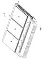
- FIG. 1is a perspective view of a module 10 devised in accordance with an embodiment of the present invention.
- Preferred module 10includes a flex circuit 12 populated with memory ICs 18 and adjunct IC 19 as further depicted in FIG. 2 .
- Flex circuit 12is disposed about a metallic substrate 14 that provides a form for the module.
- substrate 14is aluminum but other metallic materials may be thermally superior but more costly such as, for example, copper.
- Flex circuit 12is preferably made from conductive layers supported by one or more flexible substrate layers as further described with reference to later Figs. The construction of flex circuitry is known in the art.
- the entirety of the flex circuit 12may be flexible or, as those of skill in the art will recognize, the flexible circuit structure 12 may be made flexible in certain areas to allow conformability to required shapes or bends, and rigid in other areas to provide rigid and planar mounting surfaces.
- ICs 18 on flexible circuit 12may be leaded, CSP or bare die.
- leaded packaged flash memory devicesare represented as ICs 18 .
- Other types of memory devicesmay be aggregated according to the invention but preferred modules are devised for aggregation of flash memory.
- flash memoryis currently packaged in leaded packages but as chip-scale packaging (“CSP”) of flash memory circuitry arises, the invention may be adapted for use with such CSP packaged devices.
- CSPchip-scale packaging
- the term “leaded”shall refer to packaged circuits devices that exhibit connection between one or more integrated circuits within a plastic, metal or ceramic or hermetic casing and an environment through leads emergent from one or more peripheral sides of what is typically a rectangular package. Most often such packages exhibit plastic casings as is known in the art.
- a variety of devicescome in leaded packages and the invention is not limited to only aggregation of memory or flash memory devices.
- chip-scale or “CSP”shall refer to integrated circuitry of any function with an array package providing connection to one or more die through contacts (often embodied as “bumps” or “balls” for example) distributed across a major surface of the package or die.
- CSPdoes not refer to leaded devices.
- references to CSPare to be broadly construed to include the large variety of array devices (and not to be limited to memory only) and whether die-sized or other size such as BGA and micro BGA as well as flip-chip.
- Embodiments of the present inventionmay be employed with leaded or CSP devices or other devices in both packaged and unpackaged forms but leaded flash memory devices are a preferred memory circuitry aggregated through the invention as depicted in a preferred embodiment shown in FIG. 1 .
- Circuitry 19 shown in FIG. 2may be a buffer or control circuitry as is known in the art.
- FIG. 1depicts a top or outer side 8 of flex circuit 12 having three leaded ICs 18 .
- Other embodimentsmay have other numbers of devices mounted on side 8 of flex circuit 12 .
- Contactssuch as, for example, pads, are disposed beneath ICs 18 and later shown circuit 19 to provide conductive paths for interconnection to the ICs mounted along flex circuit 12 as appreciated by those of skill in the art.
- Flex circuit 12 of the embodiment shown in FIG. 1exhibits a contact area 11 where a plurality of contacts are presented to allow connection of the flex circuit and, by extension, those ICs mounted along flex circuit 12 , to a connective facility 13 that presents an interface through which the integrated circuitry along the flex circuit may be electrically accessed.
- Connector 13exhibits pins 15 for connection to the contacts of flex circuit 12 .
- Other connective facilities 13may exhibit differing techniques for connection to flex circuit 12 but those of skill will in the art will be able to readily accommodate such alternative connection strategies with little or no experimentation.
- Flex circuit 12is wrapped about substrate 14 to place ICs 18 that are populated along side 8 of flex circuit 12 on the outside of module 10 while those ICs that are populated along side 9 of flex circuit 12 (shown in FIG. 2B ) are disposed on the inside of exemplar module 10 .
- Substrate 14is preferably comprised of metallic material to exhibit advantageous thermal characteristics. As shown in this and later Figs., substrate 14 is preferably a planar-like member having first and second major sides proximal to which ICs along side 9 of flex circuit 12 of module 10 may be disposed when flex circuit 12 is wrapped about substrate 14 .
- FIG. 2Aillustrates a side of a flex circuit employed in an exemplar module 10 .
- flex circuit 12has three leaded ICs 18 mounted along a first half of side 8 and exhibits a plurality of contacts 22 proximal to flex edge 23 for connection of flex circuit 12 to a connective facility such as a connector as later shown.
- FIG. 2Billustrates another side 9 of flex circuit 12 as may be employed in a preferred embodiment of the present invention.
- side 9becomes an inner side of flex circuit 12 with respect to module 10 and side 8 of flex circuit 12 .
- five ICs 18are populated along side 9 of flex circuit 12 along with adjunct circuit 19 which may be a control or buffer circuitry, for example.
- adjunct circuit 19which may be a control or buffer circuitry, for example.
- three ICsare disposed along side 8 of flex circuit 12 and thus, module 10 in the depicted embodiment exhibits eight leaded ICs 18 .
- Those of skillwill recognize that other numbers of ICs 18 may be aggregated in embodiments of the invention and the invention in adaptable to ICs that are leaded or are CSPs.
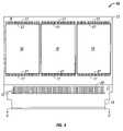
- FIG. 3is a cross-sectional depiction of a module 10 devised in accordance with a preferred embodiment of the present invention.
- Substrate 14is shown in cross-section and flex circuit 12 is depicted disposed about substrate 14 to place upper sides 16 of ICs 18 disposed along inner side 9 of flex circuit 12 adjacent to substrate 14 .
- Adhesive 30may be employed to secure ICs 18 to substrate 14 and thermally conductive adhesives are preferred.
- Pins 15are shown connected along outer side 8 of flex circuit 12 to contacts 22 (not visible in FIG. 3 ) while substrate 14 is attached to side 9 of flex circuit 12 proximal to connector 13 as shown in this embodiment.
- substrate 14may be devised in a variety of configurations and materials to provide, for example, an appropriate radius for the flex to transit about the substrate or wells into which module ICs may be disposed.
- FIG. 4depicts a plan view of a module 10 devised in accordance with a preferred embodiment of the present invention. Illustrated module 10 exhibits three flash memory leaded package ICs 18 disposed along side 8 of flex circuit 12 . Those of skill will recognize that the present invention will be advantageous in aggregating fewer or more ICs 18 than the eight depicted in the earlier Figs. ICs 18 exhibit leads 17 emergent from peripheral sides 21 of ICs 18 . Pins 15 of connector 13 are soldered in the depicted preferred embodiment to pads 22 of connective area 11 of flex circuit 12 .
- FIG. 5depicts an enlarged view of the area marked with “B” in FIG. 3 . Shown are ICs 18 mounted along flex circuit 12 with two of the ICs 18 that are mounted along inner side 9 of flex circuit 12 being shown with their respective upper sides 16 in proximity to substrate 14 which exhibits transit 14 A to allow preferred multi-layer flex circuit 12 to transit about the substrate in the depicted preferred embodiment.
- FIG. 6is an enlarged view of a portion of module 10 identified by “A” in FIG. 3 .
- Connector 31is shown with solder pins 15 attached to flex circuit 12 while substrate 14 is attached to flex circuit 12 with adhesive 30 .
- Major sides 24 and 25 of substrate 14are identified in this enlarged view.
- IC 18 populated along side 9 of flex circuit 12is shown disposed proximal to one of the two major sides of substrate 14 . Depicted IC 18 may either contact substrate 14 along parts or all of its upper surface 16 or it may be located proximal to substrate 14 but distanced from it by adhesive which in preferred embodiments is a thermally conductive adhesive.
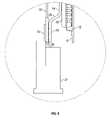
- FIG. 7is a cross-sectional view of a module 10 M disposed in enclosure “E” to present a compact flash module for connection to an environment through exemplar 50 pin connector 31 .
- Enclosure Emay be comprised of a variety of materials such as, for example, high impact resistant plastics being just one of many preferred variations that those of skill will be able to select in accordance with this invention and the relevant operating environment and manufacturing and cost constraints.
- Upper surface 16 of an IC 18may be attached to enclosure E with adhesive 30 as represented in FIG. 7 .
- a portion of surface 8 of flex circuit 12may also be affixed to enclosure E to provide a more integrated enclosed module.
- FIG. 7portrays a medial line SM depicting a plane through substrate 14 and a medial line F M demarking a plane through flex circuit 12 on one side of substrate 14 .
- Three layers of ICsare identified by references L 1 , L 2 , and L 3 .
- two layers of ICswhich comprise, in the exemplar module 10 M depicted in FIG. 7 , two layers of flash memory are depicted on one side of substrate 14 while a third layer of ICs are shown on the other side of substrate 14 . Consequently, in the depicted module, three layers of memory are shown aggregated in exemplar module 10 M.
- FIG. 8depicts a perspective view of a preferred compact flash module 10 M in accordance with the present invention that is devised to provide flash memory capability for a variety of systems and products.
- the particular preferred embodiment shown in FIG. 8is configured with mounting structures 35 to provide ready mating with application structures to affix module 10 M to the environment while electrical communication between the environment and module 10 M is provided through connector 31 .
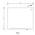
- FIG. 9depicts an exemplar module 10 M with enclosure E and connector 31 for connection to the ICs 18 and, typically, IC 19 within enclosure E.
- the depiction of FIG. 9illustrates the dimensions of a typical module 10 M that provides flash memory storage with eight flash memory ICs 18 as earlier depicted.
- Dimension Xis approximately 42 mm.
- dimension Yis approximately 36 mm. although those of skill will appreciate that these dimensions are arbitrary and modules 10 M in accordance with the present invention may be devised that illustrate a large variety of dimensions and that enclosure E may, for example, be configured in a variety of configurations to make module 10 M mechanically adaptable to a multiplicity of applications.
- FIG. 10is an exploded depiction of a flex circuit 12 cross-section according to one embodiment of the present invention.
- the depicted preferred flex circuit 12has four conductive layers 101 - 104 and seven insulative layers 105 - 111 .
- the numbers of layers describedare merely those of one preferred embodiment, and other numbers and layer arrangements may be used.
- Top conductive layer 101 and the other conductive layersare preferably made of a conductive metal such as, for example, copper or copper alloy.
- conductive layers 101 , 102 , and 104express signal traces 112 that make various connections on flex circuit 12 .
- These layersmay also express conductive planes for ground, power, or reference voltage.
- top conductive layer 101may also be provided with a flood, or plane, of to provide the VDD to ICs mounted to flex circuit 12 .
- inner conductive layer 102expresses traces connecting to and among the various devices mounted along the sides of flex circuit 12 .
- the function of any of the depicted conductive layersmay, of course, be interchanged with others of the conductive layers.
- Inner conductive layer 103expresses a ground plane, which may be split to provide VDD return for pre-register address signals.
- Inner conductive layer 103may further express other planes and traces. In this embodiment, floods, or planes, at bottom conductive layer 104 provides VREF and ground in addition to the depicted traces.
- Insulative layers 105 and 111are, in this embodiment, dielectric solder mask layers which may be deposited on the adjacent conductive layers. Insulative layers 107 and 109 are made of adhesive dielectric. Other embodiments may not have such adhesive dielectric layers. Insulative layers 106 , 108 , and 110 are preferably flexible dielectric substrate layers made of polyamide. Any other suitable flexible circuit substrate material may be used.
Landscapes
- Engineering & Computer Science (AREA)
- Microelectronics & Electronic Packaging (AREA)
- Semiconductor Memories (AREA)
- Coupling Device And Connection With Printed Circuit (AREA)
- Combinations Of Printed Boards (AREA)
- Structure Of Printed Boards (AREA)
Abstract
Description
Claims (13)
Priority Applications (2)
| Application Number | Priority Date | Filing Date | Title |
|---|---|---|---|
| US11/187,269US7606050B2 (en) | 2004-09-03 | 2005-07-22 | Compact module system and method |
| PCT/US2006/007193WO2006121489A2 (en) | 2005-05-06 | 2006-02-28 | Compact module system and method |
Applications Claiming Priority (5)
| Application Number | Priority Date | Filing Date | Title |
|---|---|---|---|
| US10/934,027US20060050492A1 (en) | 2004-09-03 | 2004-09-03 | Thin module system and method |
| US11/007,551US7511968B2 (en) | 2004-09-03 | 2004-12-08 | Buffered thin module system and method |
| US11/068,688US7324352B2 (en) | 2004-09-03 | 2005-03-01 | High capacity thin module system and method |
| US11/123,721US20060053345A1 (en) | 2004-09-03 | 2005-05-06 | Thin module system and method |
| US11/187,269US7606050B2 (en) | 2004-09-03 | 2005-07-22 | Compact module system and method |
Related Parent Applications (1)
| Application Number | Title | Priority Date | Filing Date |
|---|---|---|---|
| US11/123,721Continuation-In-PartUS20060053345A1 (en) | 2004-09-03 | 2005-05-06 | Thin module system and method |
Publications (2)
| Publication Number | Publication Date |
|---|---|
| US20060050592A1 US20060050592A1 (en) | 2006-03-09 |
| US7606050B2true US7606050B2 (en) | 2009-10-20 |
Family
ID=37397021
Family Applications (1)
| Application Number | Title | Priority Date | Filing Date |
|---|---|---|---|
| US11/187,269Expired - LifetimeUS7606050B2 (en) | 2004-09-03 | 2005-07-22 | Compact module system and method |
Country Status (2)
| Country | Link |
|---|---|
| US (1) | US7606050B2 (en) |
| WO (1) | WO2006121489A2 (en) |
Cited By (4)
| Publication number | Priority date | Publication date | Assignee | Title |
|---|---|---|---|---|
| US20120235290A1 (en)* | 2009-10-07 | 2012-09-20 | Valeo Etudes Electroniques | Power module for an automobile |
| US20130208432A1 (en)* | 2010-10-25 | 2013-08-15 | Korea Electric Terminal Co., Ltd. | Printed circuit board, and board block for vehicles using the same |
| US8971045B1 (en)* | 2004-04-09 | 2015-03-03 | Netlist, Inc. | Module having at least one thermally conductive layer between printed circuit boards |
| US20180255659A1 (en)* | 2015-08-27 | 2018-09-06 | Continental Automotive Gmbh | Electronic device having a housing with a circuit board provided therein |
Families Citing this family (35)
| Publication number | Priority date | Publication date | Assignee | Title |
|---|---|---|---|---|
| US7442050B1 (en) | 2005-08-29 | 2008-10-28 | Netlist, Inc. | Circuit card with flexible connection for memory module with heat spreader |
| US7259452B2 (en)* | 2005-10-11 | 2007-08-21 | Staktek Group L.P. | Leaded package integrated circuit stacking |
| US7508069B2 (en)* | 2006-01-11 | 2009-03-24 | Entorian Technologies, Lp | Managed memory component |
| US7508058B2 (en) | 2006-01-11 | 2009-03-24 | Entorian Technologies, Lp | Stacked integrated circuit module |
| US20080225476A1 (en)* | 2006-01-11 | 2008-09-18 | Chris Karabatsos | Tab wrap foldable electronic assembly module and method of manufacture |
| US20070164416A1 (en)* | 2006-01-17 | 2007-07-19 | James Douglas Wehrly | Managed memory component |
| US7619893B1 (en) | 2006-02-17 | 2009-11-17 | Netlist, Inc. | Heat spreader for electronic modules |
| US7393226B2 (en)* | 2006-03-08 | 2008-07-01 | Microelectronics Assembly Technologies, Inc. | Thin multichip flex-module |
| US7394149B2 (en) | 2006-03-08 | 2008-07-01 | Microelectronics Assembly Technologies, Inc. | Thin multichip flex-module |
| US7520781B2 (en) | 2006-03-08 | 2009-04-21 | Microelectronics Assembly Technologies | Thin multichip flex-module |
| US7429788B2 (en) | 2006-03-08 | 2008-09-30 | Microelectronics Assembly Technologies, Inc. | Thin multichip flex-module |
| US7787254B2 (en)* | 2006-03-08 | 2010-08-31 | Microelectronics Assembly Technologies, Inc. | Thin multichip flex-module |
| US20070211711A1 (en)* | 2006-03-08 | 2007-09-13 | Clayton James E | Thin multichip flex-module |
| US20080002447A1 (en)* | 2006-06-29 | 2008-01-03 | Smart Modular Technologies, Inc. | Memory supermodule utilizing point to point serial data links |
| US20090166065A1 (en)* | 2008-01-02 | 2009-07-02 | Clayton James E | Thin multi-chip flex module |
| US8018723B1 (en) | 2008-04-30 | 2011-09-13 | Netlist, Inc. | Heat dissipation for electronic modules |
| KR101796116B1 (en) | 2010-10-20 | 2017-11-10 | 삼성전자 주식회사 | Semiconductor device, memory module and memory system having the same and operating method thereof |
| USD716310S1 (en)* | 2012-06-09 | 2014-10-28 | Apple, Inc. | Electronic device |
| US8899994B2 (en) | 2012-10-17 | 2014-12-02 | Microelectronics Assembly Technologies, Inc. | Compression connector system |
| US8834182B2 (en) | 2012-10-17 | 2014-09-16 | Microelectronics Assembly Technologies | Pierced flexible circuit and compression joint |
| US8902606B2 (en) | 2012-10-17 | 2014-12-02 | Microelectronics Assembly Technologies | Electronic interconnect system |
| US8837141B2 (en) | 2012-10-17 | 2014-09-16 | Microelectronics Assembly Technologies | Electronic module with heat spreading enclosure |
| US9338895B2 (en)* | 2012-10-17 | 2016-05-10 | Microelectronics Assembly Technologies | Method for making an electrical circuit |
| US8817458B2 (en) | 2012-10-17 | 2014-08-26 | Microelectronics Assembly Technologies, Inc. | Flexible circuit board and connection system |
| US10679722B2 (en) | 2016-08-26 | 2020-06-09 | Sandisk Technologies Llc | Storage system with several integrated components and method for use therewith |
| TWD189067S (en)* | 2017-02-17 | 2018-03-11 | 三星電子股份有限公司 | Ssd storage device |
| TWD189065S (en)* | 2017-02-17 | 2018-03-11 | 三星電子股份有限公司 | Ssd storage device |
| TWD189066S (en)* | 2017-02-17 | 2018-03-11 | 三星電子股份有限公司 | Ssd storage device |
| TWD189068S (en)* | 2017-02-17 | 2018-03-11 | 三星電子股份有限公司 | Ssd storage device |
| TWD189071S (en)* | 2017-02-17 | 2018-03-11 | 三星電子股份有限公司 | Ssd storage device |
| TWD189069S (en)* | 2017-02-17 | 2018-03-11 | 三星電子股份有限公司 | Ssd storage device |
| TWD189070S (en)* | 2017-02-17 | 2018-03-11 | 三星電子股份有限公司 | Ssd storage device |
| TWD190983S (en)* | 2017-02-17 | 2018-06-11 | 三星電子股份有限公司 | Ssd storage device |
| USD869470S1 (en)* | 2018-04-09 | 2019-12-10 | Samsung Electronics Co., Ltd. | SSD storage device |
| USD869469S1 (en)* | 2018-04-09 | 2019-12-10 | Samsung Electronics Co., Ltd. | SSD storage device |
Citations (297)
| Publication number | Priority date | Publication date | Assignee | Title |
|---|---|---|---|---|
| US3372310A (en) | 1965-04-30 | 1968-03-05 | Radiation Inc | Universal modular packages for integrated circuits |
| US3436604A (en) | 1966-04-25 | 1969-04-01 | Texas Instruments Inc | Complex integrated circuit array and method for fabricating same |
| US3582865A (en) | 1969-12-16 | 1971-06-01 | Ibm | Microcircuit module and connector |
| US3654394A (en) | 1969-07-08 | 1972-04-04 | Gordon Eng Co | Field effect transistor switch, particularly for multiplexing |
| US3704455A (en) | 1971-02-01 | 1972-11-28 | Alfred D Scarbrough | 3d-coaxial memory construction and method of making |
| US3718842A (en) | 1972-04-21 | 1973-02-27 | Texas Instruments Inc | Liquid crystal display mounting structure |
| US3727064A (en) | 1971-03-17 | 1973-04-10 | Monsanto Co | Opto-isolator devices and method for the fabrication thereof |
| US3746934A (en) | 1971-05-06 | 1973-07-17 | Siemens Ag | Stack arrangement of semiconductor chips |
| US3766439A (en)* | 1972-01-12 | 1973-10-16 | Gen Electric | Electronic module using flexible printed circuit board with heat sink means |
| US3772776A (en) | 1969-12-03 | 1973-11-20 | Thomas & Betts Corp | Method of interconnecting memory plane boards |
| US3873889A (en)* | 1973-08-08 | 1975-03-25 | Sperry Rand Corp | Indicator module and method of manufacturing same |
| JPS5385159U (en) | 1976-12-15 | 1978-07-13 | ||
| US4169642A (en) | 1976-09-16 | 1979-10-02 | E. I. Du Pont De Nemours And Company | Integrated circuit connector |
| US4288841A (en) | 1979-09-20 | 1981-09-08 | Bell Telephone Laboratories, Incorporated | Double cavity semiconductor chip carrier |
| US4342069A (en) | 1979-07-02 | 1982-07-27 | Mostek Corporation | Integrated circuit package |
| JPS5896756A (en) | 1981-12-04 | 1983-06-08 | Toshiba Corp | multi-chip package |
| US4429349A (en) | 1980-09-30 | 1984-01-31 | Burroughs Corporation | Coil connector |
| US4437235A (en) | 1980-12-29 | 1984-03-20 | Honeywell Information Systems Inc. | Integrated circuit package |
| GB2130025A (en) | 1982-11-08 | 1984-05-23 | Control Data Corp | Memory board stacking module |
| US4513368A (en) | 1981-05-22 | 1985-04-23 | Data General Corporation | Digital data processing system having object-based logical memory addressing and self-structuring modular memory |
| US4547834A (en) | 1982-12-30 | 1985-10-15 | Thomson-Csf | Structure for assembling complex electronic circuits |
| US4567543A (en) | 1983-02-15 | 1986-01-28 | Motorola, Inc. | Double-sided flexible electronic circuit module |
| US4587596A (en) | 1984-04-09 | 1986-05-06 | Amp Incorporated | High density mother/daughter circuit board connector |
| US4645944A (en) | 1983-09-05 | 1987-02-24 | Matsushita Electric Industrial Co., Ltd. | MOS register for selecting among various data inputs |
| US4656605A (en) | 1983-09-02 | 1987-04-07 | Wang Laboratories, Inc. | Single in-line memory module |
| US4672421A (en) | 1984-04-02 | 1987-06-09 | Motorola, Inc. | Semiconductor packaging and method |
| US4682207A (en) | 1982-03-17 | 1987-07-21 | Fujitsu Limited | Semiconductor device including leadless packages and a base plate for mounting the leadless packages |
| US4696525A (en) | 1985-12-13 | 1987-09-29 | Amp Incorporated | Socket for stacking integrated circuit packages |
| US4709300A (en) | 1986-05-05 | 1987-11-24 | Itt Gallium Arsenide Technology Center, A Division Of Itt Corporation | Jumper for a semiconductor assembly |
| US4724611A (en) | 1985-08-23 | 1988-02-16 | Nec Corporation | Method for producing semiconductor module |
| US4727513A (en) | 1983-09-02 | 1988-02-23 | Wang Laboratories, Inc. | Signal in-line memory module |
| US4733461A (en) | 1984-12-28 | 1988-03-29 | Micro Co., Ltd. | Method of stacking printed circuit boards |
| US4739589A (en) | 1985-07-12 | 1988-04-26 | Wacker-Chemitronic Gesellschaft Fur Elektronik-Grundstoff Mbh | Process and apparatus for abrasive machining of a wafer-like workpiece |
| US4763188A (en) | 1986-08-08 | 1988-08-09 | Thomas Johnson | Packaging system for multiple semiconductor devices |
| US4771366A (en) | 1987-07-06 | 1988-09-13 | International Business Machines Corporation | Ceramic card assembly having enhanced power distribution and cooling |
| US4821007A (en) | 1987-02-06 | 1989-04-11 | Tektronix, Inc. | Strip line circuit component and method of manufacture |
| US4823234A (en) | 1985-08-16 | 1989-04-18 | Dai-Ichi Seiko Co., Ltd. | Semiconductor device and its manufacture |
| US4833568A (en) | 1988-01-29 | 1989-05-23 | Berhold G Mark | Three-dimensional circuit component assembly and method corresponding thereto |
| US4850892A (en) | 1985-12-16 | 1989-07-25 | Wang Laboratories, Inc. | Connecting apparatus for electrically connecting memory modules to a printed circuit board |
| US4862249A (en) | 1987-04-17 | 1989-08-29 | Xoc Devices, Inc. | Packaging system for stacking integrated circuits |
| US4911643A (en) | 1988-10-11 | 1990-03-27 | Beta Phase, Inc. | High density and high signal integrity connector |
| US4953060A (en) | 1989-05-05 | 1990-08-28 | Ncr Corporation | Stackable integrated circuit chip package with improved heat removal |
| US4956694A (en) | 1988-11-04 | 1990-09-11 | Dense-Pac Microsystems, Inc. | Integrated circuit chip stacking |
| US4972580A (en) | 1988-06-24 | 1990-11-27 | Kabushiki Kaisha Toshiba | Method for connecting electronic components with dummy patterns |
| US4982265A (en) | 1987-06-24 | 1991-01-01 | Hitachi, Ltd. | Semiconductor integrated circuit device and method of manufacturing the same |
| US4983533A (en) | 1987-10-28 | 1991-01-08 | Irvine Sensors Corporation | High-density electronic modules - process and product |
| US4985703A (en) | 1988-02-03 | 1991-01-15 | Nec Corporation | Analog multiplexer |
| US4992849A (en) | 1989-02-15 | 1991-02-12 | Micron Technology, Inc. | Directly bonded board multiple integrated circuit module |
| US4992850A (en) | 1989-02-15 | 1991-02-12 | Micron Technology, Inc. | Directly bonded simm module |
| JPH03102862A (en) | 1989-09-18 | 1991-04-30 | Fujitsu Ltd | Semiconductor device |
| US5014161A (en) | 1985-07-22 | 1991-05-07 | Digital Equipment Corporation | System for detachably mounting semiconductors on conductor substrate |
| US5014115A (en) | 1987-11-16 | 1991-05-07 | Motorola, Inc. | Coplanar waveguide semiconductor package |
| US5016138A (en) | 1987-10-27 | 1991-05-14 | Woodman John K | Three dimensional integrated circuit package |
| US5025306A (en) | 1988-08-09 | 1991-06-18 | Texas Instruments Incorporated | Assembly of semiconductor chips |
| US5034350A (en) | 1987-09-23 | 1991-07-23 | Sgs Thomson Microelectronics S.R.L. | Semiconductor device package with dies mounted on both sides of the central pad of a metal frame |
| US5041015A (en) | 1990-03-30 | 1991-08-20 | Cal Flex, Inc. | Electrical jumper assembly |
| US5053853A (en) | 1990-05-08 | 1991-10-01 | International Business Machines Corporation | Modular electronic packaging system |
| US5065277A (en) | 1990-07-13 | 1991-11-12 | Sun Microsystems, Inc. | Three dimensional packaging arrangement for computer systems and the like |
| US5099393A (en) | 1991-03-25 | 1992-03-24 | International Business Machines Corporation | Electronic package for high density applications |
| US5104820A (en) | 1989-07-07 | 1992-04-14 | Irvine Sensors Corporation | Method of fabricating electronic circuitry unit containing stacked IC layers having lead rerouting |
| US5109318A (en) | 1990-05-07 | 1992-04-28 | International Business Machines Corporation | Pluggable electronic circuit package assembly with snap together heat sink housing |
| US5117282A (en) | 1990-10-29 | 1992-05-26 | Harris Corporation | Stacked configuration for integrated circuit devices |
| US5119269A (en) | 1989-08-23 | 1992-06-02 | Seiko Epson Corporation | Semiconductor with a battery unit |
| US5138430A (en) | 1991-06-06 | 1992-08-11 | International Business Machines Corporation | High performance versatile thermally enhanced IC chip mounting |
| US5138434A (en) | 1991-01-22 | 1992-08-11 | Micron Technology, Inc. | Packaging for semiconductor logic devices |
| US5140405A (en) | 1990-08-30 | 1992-08-18 | Micron Technology, Inc. | Semiconductor assembly utilizing elastomeric single axis conductive interconnect |
| US5159535A (en) | 1987-03-11 | 1992-10-27 | International Business Machines Corporation | Method and apparatus for mounting a flexible film semiconductor chip carrier on a circuitized substrate |
| US5173840A (en) | 1990-05-07 | 1992-12-22 | Mitsubishi Denki Kabushiki Kaisha | Molded ic card |
| JPH0529534A (en) | 1991-07-25 | 1993-02-05 | Nec Corp | Memory module |
| US5191404A (en) | 1989-12-20 | 1993-03-02 | Digital Equipment Corporation | High density memory array packaging |
| US5208729A (en) | 1992-02-14 | 1993-05-04 | International Business Machines Corporation | Multi-chip module |
| US5214845A (en) | 1992-05-11 | 1993-06-01 | Micron Technology, Inc. | Method for producing high speed integrated circuits |
| US5219377A (en) | 1992-01-17 | 1993-06-15 | Texas Instruments Incorporated | High temperature co-fired ceramic integrated phased array package |
| US5222014A (en) | 1992-03-02 | 1993-06-22 | Motorola, Inc. | Three-dimensional multi-chip pad array carrier |
| US5224023A (en) | 1992-02-10 | 1993-06-29 | Smith Gary W | Foldable electronic assembly module |
| US5229916A (en) | 1992-03-04 | 1993-07-20 | International Business Machines Corporation | Chip edge interconnect overlay element |
| US5229917A (en) | 1992-07-24 | 1993-07-20 | The United States Of America As Represented By The Secretary Of The Air Force | VLSI integration into a 3-D WSI dual composite module |
| US5239198A (en) | 1989-09-06 | 1993-08-24 | Motorola, Inc. | Overmolded semiconductor device having solder ball and edge lead connective structure |
| US5241456A (en) | 1990-07-02 | 1993-08-31 | General Electric Company | Compact high density interconnect structure |
| US5241454A (en) | 1992-01-22 | 1993-08-31 | International Business Machines Corporation | Mutlilayered flexible circuit package |
| US5247423A (en) | 1992-05-26 | 1993-09-21 | Motorola, Inc. | Stacking three dimensional leadless multi-chip module and method for making the same |
| US5252857A (en) | 1991-08-05 | 1993-10-12 | International Business Machines Corporation | Stacked DCA memory chips |
| US5261068A (en) | 1990-05-25 | 1993-11-09 | Dell Usa L.P. | Dual path memory retrieval system for an interleaved dynamic RAM memory unit |
| US5259770A (en) | 1992-03-19 | 1993-11-09 | Amp Incorporated | Impedance controlled elastomeric connector |
| US5268815A (en) | 1992-02-14 | 1993-12-07 | International Business Machines Corporation | High density, high performance memory circuit package |
| JPH05335695A (en) | 1992-06-02 | 1993-12-17 | Nec Corp | Single in-line module |
| US5276418A (en) | 1988-11-16 | 1994-01-04 | Motorola, Inc. | Flexible substrate electronic assembly |
| US5281852A (en) | 1991-12-10 | 1994-01-25 | Normington Peter J C | Semiconductor device including stacked die |
| US5285398A (en)* | 1992-05-15 | 1994-02-08 | Mobila Technology Inc. | Flexible wearable computer |
| US5289062A (en) | 1991-03-18 | 1994-02-22 | Quality Semiconductor, Inc. | Fast transmission gate switch |
| US5309986A (en) | 1992-11-30 | 1994-05-10 | Satomi Itoh | Heat pipe |
| US5313097A (en) | 1992-11-16 | 1994-05-17 | International Business Machines, Corp. | High density memory module |
| US5347428A (en) | 1992-12-03 | 1994-09-13 | Irvine Sensors Corporation | Module comprising IC memory stack dedicated to and structurally combined with an IC microprocessor chip |
| US5362656A (en)* | 1992-12-02 | 1994-11-08 | Intel Corporation | Method of making an electronic assembly having a flexible circuit wrapped around a substrate |
| US5386341A (en) | 1993-11-01 | 1995-01-31 | Motorola, Inc. | Flexible substrate folded in a U-shape with a rigidizer plate located in the notch of the U-shape |
| US5394300A (en) | 1992-09-04 | 1995-02-28 | Mitsubishi Denki Kabushiki Kaisha | Thin multilayered IC memory card |
| US5397916A (en) | 1991-12-10 | 1995-03-14 | Normington; Peter J. C. | Semiconductor device including stacked die |
| US5400003A (en) | 1992-08-19 | 1995-03-21 | Micron Technology, Inc. | Inherently impedance matched integrated circuit module |
| US5428190A (en) | 1993-07-02 | 1995-06-27 | Sheldahl, Inc. | Rigid-flex board with anisotropic interconnect and method of manufacture |
| US5438224A (en) | 1992-04-23 | 1995-08-01 | Motorola, Inc. | Integrated circuit package having a face-to-face IC chip arrangement |
| US5448511A (en) | 1994-06-01 | 1995-09-05 | Storage Technology Corporation | Memory stack with an integrated interconnect and mounting structure |
| US5477082A (en) | 1994-01-11 | 1995-12-19 | Exponential Technology, Inc. | Bi-planar multi-chip module |
| US5491612A (en) | 1995-02-21 | 1996-02-13 | Fairchild Space And Defense Corporation | Three-dimensional modular assembly of integrated circuits |
| US5502333A (en) | 1994-03-30 | 1996-03-26 | International Business Machines Corporation | Semiconductor stack structures and fabrication/sparing methods utilizing programmable spare circuit |
| US5523695A (en) | 1994-08-26 | 1996-06-04 | Vlsi Technology, Inc. | Universal test socket for exposing the active surface of an integrated circuit in a die-down package |
| US5523619A (en) | 1993-11-03 | 1996-06-04 | International Business Machines Corporation | High density memory structure |
| US5541812A (en) | 1995-05-22 | 1996-07-30 | Burns; Carmen D. | Bus communication system for stacked high density integrated circuit packages having an intermediate lead frame |
| US5572065A (en) | 1992-06-26 | 1996-11-05 | Staktek Corporation | Hermetically sealed ceramic integrated circuit heat dissipating package |
| US5600178A (en) | 1993-10-08 | 1997-02-04 | Texas Instruments Incorporated | Semiconductor package having interdigitated leads |
| US5612570A (en) | 1995-04-13 | 1997-03-18 | Dense-Pac Microsystems, Inc. | Chip stack and method of making same |
| US5631193A (en) | 1992-12-11 | 1997-05-20 | Staktek Corporation | High density lead-on-package fabrication method |
| US5642055A (en) | 1990-02-14 | 1997-06-24 | Particle Interconnect, Inc. | Electrical interconnect using particle enhanced joining of metal surfaces |
| US5644161A (en) | 1993-03-29 | 1997-07-01 | Staktek Corporation | Ultra-high density warp-resistant memory module |
| US5646446A (en)* | 1995-12-22 | 1997-07-08 | Fairchild Space And Defense Corporation | Three-dimensional flexible assembly of integrated circuits |
| US5654877A (en) | 1991-08-15 | 1997-08-05 | Staktek Corporation | Lead-on-chip integrated circuit apparatus |
| US5661339A (en) | 1992-09-16 | 1997-08-26 | Clayton; James E. | Thin multichip module |
| US5686730A (en) | 1995-05-15 | 1997-11-11 | Silicon Graphics, Inc. | Dimm pair with data memory and state memory |
| US5688606A (en)* | 1995-04-26 | 1997-11-18 | Olin Corporation | Anodized aluminum substrate having increased breakdown voltage |
| US5708297A (en) | 1992-09-16 | 1998-01-13 | Clayton; James E. | Thin multichip module |
| US5714802A (en) | 1991-06-18 | 1998-02-03 | Micron Technology, Inc. | High-density electronic module |
| US5717556A (en) | 1995-04-26 | 1998-02-10 | Nec Corporation | Printed-wiring board having plural parallel-connected interconnections |
| US5729894A (en) | 1992-07-21 | 1998-03-24 | Lsi Logic Corporation | Method of assembling ball bump grid array semiconductor packages |
| US5744862A (en) | 1996-03-29 | 1998-04-28 | Mitsubishi Denki Kabushiki Kaisha | Reduced thickness semiconductor device with IC packages mounted in openings on substrate |
| US5754409A (en)* | 1996-11-06 | 1998-05-19 | Dynamem, Inc. | Foldable electronic assembly module |
| US5764497A (en) | 1995-11-13 | 1998-06-09 | Minolta Co, Ltd. | Circuit board connection method and connection structure |
| US5789815A (en)* | 1996-04-23 | 1998-08-04 | Motorola, Inc. | Three dimensional semiconductor package having flexible appendages |
| US5790447A (en) | 1995-05-15 | 1998-08-04 | Silicon Graphics, Inc. | High-memory capacity DIMM with data and state memory |
| US5802395A (en) | 1996-07-08 | 1998-09-01 | International Business Machines Corporation | High density memory modules with improved data bus performance |
| US5805422A (en) | 1994-09-21 | 1998-09-08 | Nec Corporation | Semiconductor package with flexible board and method of fabricating the same |
| US5835988A (en) | 1996-03-27 | 1998-11-10 | Mitsubishi Denki Kabushiki Kaisha | Packed semiconductor device with wrap around external leads |
| US5869353A (en) | 1997-11-17 | 1999-02-09 | Dense-Pac Microsystems, Inc. | Modular panel stacking process |
| US5899705A (en) | 1997-11-20 | 1999-05-04 | Akram; Salman | Stacked leads-over chip multi-chip module |
| US5917709A (en) | 1997-06-16 | 1999-06-29 | Eastman Kodak Company | Multiple circuit board assembly having an interconnect mechanism that includes a flex connector |
| US5925934A (en) | 1995-10-28 | 1999-07-20 | Institute Of Microelectronics | Low cost and highly reliable chip-sized package |
| US5926369A (en)* | 1998-01-22 | 1999-07-20 | International Business Machines Corporation | Vertically integrated multi-chip circuit package with heat-sink support |
| US5949657A (en) | 1997-12-01 | 1999-09-07 | Karabatsos; Chris | Bottom or top jumpered foldable electronic assembly |
| US5953214A (en) | 1994-03-07 | 1999-09-14 | International Business Machines Corporation | Dual substrate package assembly coupled to a conducting member |
| US5953215A (en) | 1997-12-01 | 1999-09-14 | Karabatsos; Chris | Apparatus and method for improving computer memory speed and capacity |
| US5959839A (en) | 1997-01-02 | 1999-09-28 | At&T Corp | Apparatus for heat removal using a flexible backplane |
| US5963427A (en) | 1997-12-11 | 1999-10-05 | Sun Microsystems, Inc. | Multi-chip module with flexible circuit board |
| US5969945A (en)* | 1993-06-03 | 1999-10-19 | International Business Machines Corporation | Electronic package assembly |
| US5973395A (en) | 1996-04-30 | 1999-10-26 | Yamaichi Electronics Co., Ltd. | IC package having a single wiring sheet with a lead pattern disposed thereon |
| US5995370A (en) | 1997-09-01 | 1999-11-30 | Sharp Kabushiki Kaisha | Heat-sinking arrangement for circuit elements |
| US6002589A (en) | 1997-07-21 | 1999-12-14 | Rambus Inc. | Integrated circuit package for coupling to a printed circuit board |
| US6002167A (en) | 1995-09-22 | 1999-12-14 | Hitachi Cable, Ltd. | Semiconductor device having lead on chip structure |
| US6008538A (en) | 1996-10-08 | 1999-12-28 | Micron Technology, Inc. | Method and apparatus providing redundancy for fabricating highly reliable memory modules |
| US6014316A (en) | 1997-06-13 | 2000-01-11 | Irvine Sensors Corporation | IC stack utilizing BGA contacts |
| US6021048A (en) | 1998-02-17 | 2000-02-01 | Smith; Gary W. | High speed memory module |
| US6025992A (en)* | 1999-02-11 | 2000-02-15 | International Business Machines Corp. | Integrated heat exchanger for memory module |
| US6028365A (en) | 1998-03-30 | 2000-02-22 | Micron Technology, Inc. | Integrated circuit package and method of fabrication |
| US6028352A (en) | 1997-06-13 | 2000-02-22 | Irvine Sensors Corporation | IC stack utilizing secondary leadframes |
| US6034878A (en) | 1996-12-16 | 2000-03-07 | Hitachi, Ltd. | Source-clock-synchronized memory system and memory unit |
| US6038132A (en) | 1996-12-06 | 2000-03-14 | Mitsubishi Denki Kabushiki Kaisha | Memory module |
| US6040624A (en) | 1997-10-02 | 2000-03-21 | Motorola, Inc. | Semiconductor device package and method |
| US6072233A (en) | 1998-05-04 | 2000-06-06 | Micron Technology, Inc. | Stackable ball grid array package |
| US6078515A (en) | 1998-04-14 | 2000-06-20 | Silicon Graphics, Inc. | Memory system with multiple addressing and control busses |
| US6084294A (en) | 1998-08-26 | 2000-07-04 | Mitsubishi Denki Kabushiki Kaisha | Semiconductor device comprising stacked semiconductor elements |
| US6097087A (en) | 1997-10-31 | 2000-08-01 | Micron Technology, Inc. | Semiconductor package including flex circuit, interconnects and dense array external contacts |
| US6111757A (en) | 1998-01-16 | 2000-08-29 | International Business Machines Corp. | SIMM/DIMM memory module |
| US6121676A (en) | 1996-12-13 | 2000-09-19 | Tessera, Inc. | Stacked microelectronic assembly and method therefor |
| USRE36916E (en) | 1995-03-21 | 2000-10-17 | Simple Technology Incorporated | Apparatus for stacking semiconductor chips |
| US6157541A (en) | 1997-12-30 | 2000-12-05 | Siemens Aktiengesellschaft | Stack arrangement for two semiconductor memory chips and printed board for accepting a plurality of such stack arrangements |
| US6172874B1 (en) | 1998-04-06 | 2001-01-09 | Silicon Graphics, Inc. | System for stacking of integrated circuit packages |
| US6178093B1 (en) | 1996-06-28 | 2001-01-23 | International Business Machines Corporation | Information handling system with circuit assembly having holes filled with filler material |
| US6180881B1 (en) | 1998-05-05 | 2001-01-30 | Harlan Ruben Isaak | Chip stack and method of making same |
| US6187652B1 (en) | 1998-09-14 | 2001-02-13 | Fujitsu Limited | Method of fabrication of multiple-layer high density substrate |
| JP2001077294A (en) | 1999-09-02 | 2001-03-23 | Nec Corp | Semiconductor device |
| US6208546B1 (en) | 1996-11-12 | 2001-03-27 | Niigata Seimitsu Co., Ltd. | Memory module |
| US6205654B1 (en) | 1992-12-11 | 2001-03-27 | Staktek Group L.P. | Method of manufacturing a surface mount package |
| US6208521B1 (en) | 1997-05-19 | 2001-03-27 | Nitto Denko Corporation | Film carrier and laminate type mounting structure using same |
| JP2001085592A (en) | 1999-09-17 | 2001-03-30 | Seiko Epson Corp | Semiconductor device and its manufacturing method, circuit board, and electronic equipment |
| US6215687B1 (en) | 1996-02-26 | 2001-04-10 | Hitachi, Ltd. | Semiconductor device and process for manufacturing the same |
| US6214641B1 (en) | 1996-06-25 | 2001-04-10 | Micron Technology, Inc. | Method of fabricating a multi-chip module |
| US6222739B1 (en) | 1998-01-20 | 2001-04-24 | Viking Components | High-density computer module with stacked parallel-plane packaging |
| US6222737B1 (en) | 1999-04-23 | 2001-04-24 | Dense-Pac Microsystems, Inc. | Universal package and method of forming the same |
| US6225688B1 (en) | 1997-12-11 | 2001-05-01 | Tessera, Inc. | Stacked microelectronic assembly and method therefor |
| US20010001085A1 (en) | 1999-04-16 | 2001-05-10 | Ali Hassanzadeh | Memory module with offset notches for improved insertion and memory module connector |
| US6233650B1 (en) | 1998-04-01 | 2001-05-15 | Intel Corporation | Using FET switches for large memory arrays |
| US6234820B1 (en) | 1997-07-21 | 2001-05-22 | Rambus Inc. | Method and apparatus for joining printed circuit boards |
| US6262895B1 (en) | 2000-01-13 | 2001-07-17 | John A. Forthun | Stackable chip package with flex carrier |
| US6262476B1 (en) | 1998-07-27 | 2001-07-17 | Siemens Aktiengesellschaft | Composite member composed of at least two integrated circuits and method for the manufacture of a composite member composed of at least two integrated circuits |
| US6265660B1 (en) | 1997-07-09 | 2001-07-24 | Micron Technology, Inc. | Package stack via bottom leaded plastic (BLP) packaging |
| US6266252B1 (en) | 1997-12-01 | 2001-07-24 | Chris Karabatsos | Apparatus and method for terminating a computer memory bus |
| EP1119049A2 (en) | 2000-01-18 | 2001-07-25 | Sony Corporation | Laminate type semiconductor apparatus |
| US20010013423A1 (en) | 1996-10-31 | 2001-08-16 | Hormazdyar M. Dalal | Flip chip attach on flexible circuit carrier using chip with metallic cap on solder |
| US6281577B1 (en) | 1996-06-28 | 2001-08-28 | Pac Tech-Packaging Technologies Gmbh | Chips arranged in plurality of planes and electrically connected to one another |
| US6288907B1 (en) | 1996-05-20 | 2001-09-11 | Staktek Group, L.P. | High density integrated circuit module with complex electrical interconnect rails having electrical interconnect strain relief |
| US20010026009A1 (en) | 2000-03-24 | 2001-10-04 | Kensuke Tsunesa | Semiconductor devicse, a semicinductor module loaded with said semiconductor device and a method of manufacturing said semicoductor device |
| US6300679B1 (en) | 1998-06-01 | 2001-10-09 | Semiconductor Components Industries, Llc | Flexible substrate for packaging a semiconductor component |
| US20010028588A1 (en) | 1996-11-19 | 2001-10-11 | Matsushita Electronics Corporation | Semiconductor memory |
| US20010035572A1 (en) | 1999-05-05 | 2001-11-01 | Isaak Harlan R. | Stackable flex circuit chip package and method of making same |
| US6316825B1 (en) | 1998-05-15 | 2001-11-13 | Hyundai Electronics Industries Co., Ltd. | Chip stack package utilizing a connecting hole to improve electrical connection between leadframes |
| US20010040793A1 (en) | 2000-02-01 | 2001-11-15 | Tetsuya Inaba | Electronic device and method of producing the same |
| US6323060B1 (en) | 1999-05-05 | 2001-11-27 | Dense-Pac Microsystems, Inc. | Stackable flex circuit IC package and method of making same |
| JP2001332683A (en) | 2000-05-19 | 2001-11-30 | Nec Corp | Laminated semiconductor device and manufacturing method thereof |
| US6336262B1 (en) | 1996-10-31 | 2002-01-08 | International Business Machines Corporation | Process of forming a capacitor with multi-level interconnection technology |
| JP2002009231A (en) | 2000-06-20 | 2002-01-11 | Seiko Epson Corp | Semiconductor device |
| US20020006032A1 (en) | 2000-05-23 | 2002-01-17 | Chris Karabatsos | Low-profile registered DIMM |
| US6343020B1 (en) | 1998-12-28 | 2002-01-29 | Foxconn Precision Components Co., Ltd. | Memory module |
| US6347394B1 (en) | 1998-11-04 | 2002-02-12 | Micron Technology, Inc. | Buffering circuit embedded in an integrated circuit device module used for buffering clocks and other input signals |
| US6349050B1 (en) | 2000-10-10 | 2002-02-19 | Rambus, Inc. | Methods and systems for reducing heat flux in memory systems |
| US6357023B1 (en) | 1998-04-08 | 2002-03-12 | Kingston Technology Co. | Connector assembly for testing memory modules from the solder-side of a PC motherboard with forced hot air |
| US20020030995A1 (en) | 2000-08-07 | 2002-03-14 | Masao Shoji | Headlight |
| US6358772B2 (en) | 1997-05-02 | 2002-03-19 | Nec Corporation | Semiconductor package having semiconductor element mounting structure of semiconductor package mounted on circuit board and method of assembling semiconductor package |
| US6370668B1 (en) | 1999-07-23 | 2002-04-09 | Rambus Inc | High speed memory system capable of selectively operating in non-chip-kill and chip-kill modes |
| US6376769B1 (en) | 1999-05-18 | 2002-04-23 | Amerasia International Technology, Inc. | High-density electronic package, and method for making same |
| US6392162B1 (en) | 2000-11-10 | 2002-05-21 | Chris Karabatsos | Double-sided flexible jumper assembly and method of manufacture |
| US6404043B1 (en) | 2000-06-21 | 2002-06-11 | Dense-Pac Microsystems, Inc. | Panel stacking of BGA devices to form three-dimensional modules |
| US20020076919A1 (en) | 1998-11-13 | 2002-06-20 | Peters Michael G. | Composite interposer and method for producing a composite interposer |
| US6410857B1 (en) | 2001-03-01 | 2002-06-25 | Lockheed Martin Corporation | Signal cross-over interconnect for a double-sided circuit card assembly |
| US6426560B1 (en) | 1999-08-06 | 2002-07-30 | Hitachi, Ltd. | Semiconductor device and memory module |
| US20020101261A1 (en) | 2001-02-01 | 2002-08-01 | Chris Karabatsos | Tri-directional, high-speed bus switch |
| US6433418B1 (en) | 1998-07-24 | 2002-08-13 | Fujitsu Limited | Apparatus for a vertically accumulable semiconductor device with external leads secured by a positioning mechanism |
| US6446158B1 (en) | 1999-05-17 | 2002-09-03 | Chris Karabatsos | Memory system using FET switches to select memory banks |
| US6444921B1 (en) | 2000-02-03 | 2002-09-03 | Fujitsu Limited | Reduced stress and zero stress interposers for integrated-circuit chips, multichip substrates, and the like |
| US6449159B1 (en) | 2000-05-03 | 2002-09-10 | Rambus Inc. | Semiconductor module with imbedded heat spreader |
| US6452826B1 (en) | 2000-10-26 | 2002-09-17 | Samsung Electronics Co., Ltd. | Memory module system |
| US6459152B1 (en) | 1999-10-27 | 2002-10-01 | Mitsubishi Denki Kabushiki Kaisha | Semiconductor device having a chip, reinforcing plate, and sealing material sharing a common rear surface |
| US20020139577A1 (en) | 2001-03-27 | 2002-10-03 | Miller Charles A. | In-street integrated circuit wafer via |
| US6465893B1 (en) | 1990-09-24 | 2002-10-15 | Tessera, Inc. | Stacked chip assembly |
| US20020164838A1 (en) | 2001-05-02 | 2002-11-07 | Moon Ow Chee | Flexible ball grid array chip scale packages and methods of fabrication |
| US6486544B1 (en) | 1998-09-09 | 2002-11-26 | Seiko Epson Corporation | Semiconductor device and method manufacturing the same, circuit board, and electronic instrument |
| US6489687B1 (en) | 1999-10-01 | 2002-12-03 | Seiko Epson Corporation | Semiconductor device and method of manufacturing the same, manufacturing device, circuit board, and electronic equipment |
| US20020180022A1 (en) | 1999-10-20 | 2002-12-05 | Seiko Epson Corporation | Semiconductor device |
| US20020196612A1 (en) | 2001-05-25 | 2002-12-26 | Martin Gall | Arrangement of memory chip housings on a DIMM circuit board |
| US6502161B1 (en) | 2000-01-05 | 2002-12-31 | Rambus Inc. | Memory system including a point-to-point linked memory subsystem |
| US20030002262A1 (en) | 2001-07-02 | 2003-01-02 | Martin Benisek | Electronic printed circuit board having a plurality of identically designed, housing-encapsulated semiconductor memories |
| US20030026155A1 (en) | 2001-08-01 | 2003-02-06 | Mitsubishi Denki Kabushiki Kaisha | Semiconductor memory module and register buffer device for use in the same |
| US6521984B2 (en) | 2000-11-07 | 2003-02-18 | Mitsubishi Denki Kabushiki Kaisha | Semiconductor module with semiconductor devices attached to upper and lower surface of a semiconductor substrate |
| US20030035328A1 (en) | 2001-08-08 | 2003-02-20 | Mitsubishi Denki Kabushiki Kaisha | Semiconductor memory device shiftable to test mode in module as well as semiconductor memory module using the same |
| US6528870B2 (en) | 2000-01-28 | 2003-03-04 | Kabushiki Kaisha Toshiba | Semiconductor device having a plurality of stacked wiring boards |
| US20030045025A1 (en) | 2000-01-26 | 2003-03-06 | Coyle Anthony L. | Method of fabricating a molded package for micromechanical devices |
| US20030049886A1 (en) | 2001-09-07 | 2003-03-13 | Salmon Peter C. | Electronic system modules and method of fabrication |
| JP2003086761A (en) | 2001-09-14 | 2003-03-20 | Casio Comput Co Ltd | Semiconductor device and manufacturing method thereof |
| JP2003086760A (en) | 2001-09-12 | 2003-03-20 | Hitachi Ltd | Semiconductor device and method of manufacturing the same |
| US6552910B1 (en) | 2000-06-28 | 2003-04-22 | Micron Technology, Inc. | Stacked-die assemblies with a plurality of microelectronic devices and methods of manufacture |
| US20030081392A1 (en) | 2001-10-26 | 2003-05-01 | Staktek Group, L.P. | Integrated circuit stacking system and method |
| US20030081387A1 (en) | 2001-11-01 | 2003-05-01 | Jurgen Schulz | Module and connector having multiple contact rows |
| WO2003037053A1 (en) | 2001-10-26 | 2003-05-01 | Staktek Group, L.P. | Chip scale stacking system and method |
| US6560117B2 (en) | 2000-06-28 | 2003-05-06 | Micron Technology, Inc. | Packaged microelectronic die assemblies and methods of manufacture |
| US20030089978A1 (en) | 1999-02-26 | 2003-05-15 | Hitachi, Ltd. | Memory-module and a method of manufacturing the same |
| US20030090879A1 (en) | 2001-06-14 | 2003-05-15 | Doblar Drew G. | Dual inline memory module |
| US20030096497A1 (en) | 2001-11-19 | 2003-05-22 | Micron Technology, Inc. | Electrode structure for use in an integrated circuit |
| US6572387B2 (en) | 1999-09-24 | 2003-06-03 | Staktek Group, L.P. | Flexible circuit connector for stacked chip module |
| US6573593B1 (en) | 1996-09-18 | 2003-06-03 | Infineon Technologies Ag | Integrated circuit with a housing accommodating the integrated circuit |
| US20030109078A1 (en) | 1996-12-03 | 2003-06-12 | Yoshikazu Takahashi | Semiconductor device, method for manufacturing the same, and method for mounting the same |
| US6588095B2 (en) | 2001-04-27 | 2003-07-08 | Hewlett-Packard Development Company, Lp. | Method of processing a device by electrophoresis coating |
| US6590282B1 (en)* | 2002-04-12 | 2003-07-08 | Industrial Technology Research Institute | Stacked semiconductor package formed on a substrate and method for fabrication |
| US6600222B1 (en) | 2002-07-17 | 2003-07-29 | Intel Corporation | Stacked microelectronic packages |
| US20030159278A1 (en) | 2002-02-26 | 2003-08-28 | Peddle Charles I. | Methods and apparatus for fabricating Chip-on-Board modules |
| US6614664B2 (en) | 2000-10-24 | 2003-09-02 | Samsung Electronics Co., Ltd. | Memory module having series-connected printed circuit boards |
| US20030168725A1 (en) | 1996-12-13 | 2003-09-11 | Tessera, Inc. | Methods of making microelectronic assemblies including folded substrates |
| US6627984B2 (en) | 2001-07-24 | 2003-09-30 | Dense-Pac Microsystems, Inc. | Chip stack with differing chip package types |
| US6629855B1 (en) | 1999-07-01 | 2003-10-07 | Silicon Graphics, Inc. | Memory system including guides that receive memory modules |
| JP2003309246A (en) | 2003-05-12 | 2003-10-31 | Oki Electric Ind Co Ltd | Semiconductor module |
| JP2003347503A (en) | 2002-05-30 | 2003-12-05 | Hitachi Ltd | Semiconductor device and method of manufacturing the same, and semiconductor mounting structure |
| US6661092B2 (en) | 2001-07-26 | 2003-12-09 | Elpida Memory, Inc. | Memory module |
| US6660561B2 (en) | 2000-06-15 | 2003-12-09 | Dpac Technologies Corp. | Method of assembling a stackable integrated circuit chip |
| US20040000708A1 (en) | 2001-10-26 | 2004-01-01 | Staktek Group, L.P. | Memory expansion and chip scale stacking system and method |
| US6677670B2 (en) | 2000-04-25 | 2004-01-13 | Seiko Epson Corporation | Semiconductor device |
| US20040012991A1 (en) | 2002-07-18 | 2004-01-22 | Mitsubishi Denki Kabushiki Kaisha | Semiconductor memory module |
| US6683377B1 (en) | 2000-05-30 | 2004-01-27 | Amkor Technology, Inc. | Multi-stacked memory package |
| US20040021211A1 (en) | 2002-08-05 | 2004-02-05 | Tessera, Inc. | Microelectronic adaptors, assemblies and methods |
| US6690584B2 (en) | 2000-08-14 | 2004-02-10 | Fujitsu Limited | Information-processing device having a crossbar-board connected to back panels on different sides |
| US6721185B2 (en) | 2001-05-01 | 2004-04-13 | Sun Microsystems, Inc. | Memory module having balanced data I/O contacts pads |
| US6721181B1 (en) | 2002-09-27 | 2004-04-13 | Rockwell Automation Technologies, Inc. | Elongated heat sink for use in converter assemblies |
| US20040099938A1 (en) | 2002-09-11 | 2004-05-27 | Tessera, Inc. | Assemblies having stacked semiconductor chips and methods of making same |
| US6751113B2 (en) | 2002-03-07 | 2004-06-15 | Netlist, Inc. | Arrangement of integrated circuits in a memory module |
| US6760220B2 (en) | 2002-11-25 | 2004-07-06 | Lockheed Martin Corporation | Rugged modular PC 104 chassis with blind mate connector and forced convection cooling capabilities |
| US6762942B1 (en) | 2002-09-05 | 2004-07-13 | Gary W. Smith | Break away, high speed, folded, jumperless electronic assembly |
| US6768660B2 (en) | 2001-01-08 | 2004-07-27 | Samsung Electronics Co. Ltd. | Multi-chip memory devices and modules including independent control of memory chips |
| US20040150107A1 (en) | 2002-12-31 | 2004-08-05 | Cha Ki Bon | Stack package and fabricating method thereof |
| US20040229402A1 (en) | 2001-10-26 | 2004-11-18 | Staktek Group, L.P. | Low profile chip scale stacking system and method |
| US20040236877A1 (en) | 1997-12-17 | 2004-11-25 | Lee A. Burton | Switch/network adapter port incorporating shared memory resources selectively accessible by a direct execution logic element and one or more dense logic devices in a fully buffered dual in-line memory module format (FB-DIMM) |
| US6833984B1 (en) | 2000-05-03 | 2004-12-21 | Rambus, Inc. | Semiconductor module with serial bus connection to multiple dies |
| US6833981B2 (en) | 2001-06-28 | 2004-12-21 | Hitachi, Ltd. | Spin valve magnetic head with three underlayers |
| US20050082663A1 (en) | 2003-10-20 | 2005-04-21 | Renesas Technology Corp. | Semiconductor device and semiconductor module |
| US6884653B2 (en) | 2001-03-21 | 2005-04-26 | Micron Technology, Inc. | Folded interposer |
| US20050108468A1 (en) | 2003-11-18 | 2005-05-19 | International Business Machines Corporation | Memory device with programmable receivers to improve performance |
| US20050133897A1 (en) | 2003-12-17 | 2005-06-23 | Baek Joong-Hyun | Stack package with improved heat radiation and module having the stack package mounted thereon |
| US6956284B2 (en) | 2001-10-26 | 2005-10-18 | Staktek Group L.P. | Integrated circuit stacking system and method |
| US20050242423A1 (en) | 2001-10-26 | 2005-11-03 | Staktek Group, L.P. | Stacked module systems and methods |
| US20050263911A1 (en) | 2004-05-31 | 2005-12-01 | Yusuke Igarashi | Circuit device and manufacturing method thereof |
| US6975034B2 (en)* | 2002-07-02 | 2005-12-13 | Jenoptik Laserdiode Gmbh | Semiconductor module |
| US20060020740A1 (en) | 2004-07-22 | 2006-01-26 | International Business Machines Corporation | Multi-node architecture with daisy chain communication link configurable to operate in unidirectional and bidirectional modes |
| US20060053345A1 (en) | 2004-09-03 | 2006-03-09 | Staktek Group L.P. | Thin module system and method |
| US20060050489A1 (en) | 2004-09-03 | 2006-03-09 | Staktek Group L.P. | Optimized mounting area circuit module system and method |
| US20060049513A1 (en) | 2004-09-03 | 2006-03-09 | Staktek Group L.P. | Thin module system and method with thermal management |
| US20060050496A1 (en) | 2004-09-03 | 2006-03-09 | Staktek Group L.P. | Thin module system and method |
| US20060050497A1 (en) | 2004-09-03 | 2006-03-09 | Staktek Group L.P. | Buffered thin module system and method |
| US20060095592A1 (en) | 2004-10-29 | 2006-05-04 | International Business Machines Corporation | Multi-channel memory architecture for daisy chained arrangements of nodes with bridging between memory channels |
| US20060091529A1 (en) | 2004-09-03 | 2006-05-04 | Staktek Group L.P. | High capacity thin module system and method |
| US20060111866A1 (en) | 2004-11-23 | 2006-05-25 | Leclerg Frank E | Method, apparatus, and system for memory read transaction biasing in mirrored mode to provide thermal management |
| US7053478B2 (en) | 2001-10-26 | 2006-05-30 | Staktek Group L.P. | Pitch change and chip scale stacking system |
| US20060125067A1 (en) | 2004-09-03 | 2006-06-15 | Staktek Group L.P. | Flex circuit constructions for high capacity circuit module systems and methods |
| US7180167B2 (en) | 2001-10-26 | 2007-02-20 | Staktek Group L. P. | Low profile stacking system and method |
| US20080030972A1 (en) | 2004-09-03 | 2008-02-07 | Staktek Group L.P. | High Capacity Thin Module System and Method |
Family Cites Families (1)
| Publication number | Priority date | Publication date | Assignee | Title |
|---|---|---|---|---|
| US6712226B1 (en)* | 2001-03-13 | 2004-03-30 | James E. Williams, Jr. | Wall or ceiling mountable brackets for storing and displaying board-based recreational equipment |
- 2005
- 2005-07-22USUS11/187,269patent/US7606050B2/ennot_activeExpired - Lifetime
- 2006
- 2006-02-28WOPCT/US2006/007193patent/WO2006121489A2/enactiveApplication Filing
Patent Citations (351)
| Publication number | Priority date | Publication date | Assignee | Title |
|---|---|---|---|---|
| US3372310A (en) | 1965-04-30 | 1968-03-05 | Radiation Inc | Universal modular packages for integrated circuits |
| US3436604A (en) | 1966-04-25 | 1969-04-01 | Texas Instruments Inc | Complex integrated circuit array and method for fabricating same |
| US3654394A (en) | 1969-07-08 | 1972-04-04 | Gordon Eng Co | Field effect transistor switch, particularly for multiplexing |
| US3772776A (en) | 1969-12-03 | 1973-11-20 | Thomas & Betts Corp | Method of interconnecting memory plane boards |
| US3582865A (en) | 1969-12-16 | 1971-06-01 | Ibm | Microcircuit module and connector |
| US3704455A (en) | 1971-02-01 | 1972-11-28 | Alfred D Scarbrough | 3d-coaxial memory construction and method of making |
| US3727064A (en) | 1971-03-17 | 1973-04-10 | Monsanto Co | Opto-isolator devices and method for the fabrication thereof |
| US3746934A (en) | 1971-05-06 | 1973-07-17 | Siemens Ag | Stack arrangement of semiconductor chips |
| US3766439A (en)* | 1972-01-12 | 1973-10-16 | Gen Electric | Electronic module using flexible printed circuit board with heat sink means |
| US3718842A (en) | 1972-04-21 | 1973-02-27 | Texas Instruments Inc | Liquid crystal display mounting structure |
| US3873889A (en)* | 1973-08-08 | 1975-03-25 | Sperry Rand Corp | Indicator module and method of manufacturing same |
| US4169642A (en) | 1976-09-16 | 1979-10-02 | E. I. Du Pont De Nemours And Company | Integrated circuit connector |
| JPS5385159U (en) | 1976-12-15 | 1978-07-13 | ||
| US4342069A (en) | 1979-07-02 | 1982-07-27 | Mostek Corporation | Integrated circuit package |
| US4288841A (en) | 1979-09-20 | 1981-09-08 | Bell Telephone Laboratories, Incorporated | Double cavity semiconductor chip carrier |
| US4429349A (en) | 1980-09-30 | 1984-01-31 | Burroughs Corporation | Coil connector |
| US4437235A (en) | 1980-12-29 | 1984-03-20 | Honeywell Information Systems Inc. | Integrated circuit package |
| US4513368A (en) | 1981-05-22 | 1985-04-23 | Data General Corporation | Digital data processing system having object-based logical memory addressing and self-structuring modular memory |
| JPS5896756A (en) | 1981-12-04 | 1983-06-08 | Toshiba Corp | multi-chip package |
| US4682207A (en) | 1982-03-17 | 1987-07-21 | Fujitsu Limited | Semiconductor device including leadless packages and a base plate for mounting the leadless packages |
| GB2130025A (en) | 1982-11-08 | 1984-05-23 | Control Data Corp | Memory board stacking module |
| US4547834A (en) | 1982-12-30 | 1985-10-15 | Thomson-Csf | Structure for assembling complex electronic circuits |
| US4567543A (en) | 1983-02-15 | 1986-01-28 | Motorola, Inc. | Double-sided flexible electronic circuit module |
| US4656605A (en) | 1983-09-02 | 1987-04-07 | Wang Laboratories, Inc. | Single in-line memory module |
| US4727513A (en) | 1983-09-02 | 1988-02-23 | Wang Laboratories, Inc. | Signal in-line memory module |
| US4645944A (en) | 1983-09-05 | 1987-02-24 | Matsushita Electric Industrial Co., Ltd. | MOS register for selecting among various data inputs |
| US4672421A (en) | 1984-04-02 | 1987-06-09 | Motorola, Inc. | Semiconductor packaging and method |
| US4587596A (en) | 1984-04-09 | 1986-05-06 | Amp Incorporated | High density mother/daughter circuit board connector |
| US4733461A (en) | 1984-12-28 | 1988-03-29 | Micro Co., Ltd. | Method of stacking printed circuit boards |
| US4739589A (en) | 1985-07-12 | 1988-04-26 | Wacker-Chemitronic Gesellschaft Fur Elektronik-Grundstoff Mbh | Process and apparatus for abrasive machining of a wafer-like workpiece |
| US5014161A (en) | 1985-07-22 | 1991-05-07 | Digital Equipment Corporation | System for detachably mounting semiconductors on conductor substrate |
| US4823234A (en) | 1985-08-16 | 1989-04-18 | Dai-Ichi Seiko Co., Ltd. | Semiconductor device and its manufacture |
| US4724611A (en) | 1985-08-23 | 1988-02-16 | Nec Corporation | Method for producing semiconductor module |
| US4696525A (en) | 1985-12-13 | 1987-09-29 | Amp Incorporated | Socket for stacking integrated circuit packages |
| US4850892A (en) | 1985-12-16 | 1989-07-25 | Wang Laboratories, Inc. | Connecting apparatus for electrically connecting memory modules to a printed circuit board |
| US4709300A (en) | 1986-05-05 | 1987-11-24 | Itt Gallium Arsenide Technology Center, A Division Of Itt Corporation | Jumper for a semiconductor assembly |
| US4763188A (en) | 1986-08-08 | 1988-08-09 | Thomas Johnson | Packaging system for multiple semiconductor devices |
| US4821007A (en) | 1987-02-06 | 1989-04-11 | Tektronix, Inc. | Strip line circuit component and method of manufacture |
| US5159535A (en) | 1987-03-11 | 1992-10-27 | International Business Machines Corporation | Method and apparatus for mounting a flexible film semiconductor chip carrier on a circuitized substrate |
| US4862249A (en) | 1987-04-17 | 1989-08-29 | Xoc Devices, Inc. | Packaging system for stacking integrated circuits |
| US4982265A (en) | 1987-06-24 | 1991-01-01 | Hitachi, Ltd. | Semiconductor integrated circuit device and method of manufacturing the same |
| US4771366A (en) | 1987-07-06 | 1988-09-13 | International Business Machines Corporation | Ceramic card assembly having enhanced power distribution and cooling |
| EP0298211A3 (en) | 1987-07-06 | 1991-01-16 | International Business Machines Corporation | Ceramic card assembly having enhanced power distribution and cooling |
| US5034350A (en) | 1987-09-23 | 1991-07-23 | Sgs Thomson Microelectronics S.R.L. | Semiconductor device package with dies mounted on both sides of the central pad of a metal frame |
| US5016138A (en) | 1987-10-27 | 1991-05-14 | Woodman John K | Three dimensional integrated circuit package |
| US4983533A (en) | 1987-10-28 | 1991-01-08 | Irvine Sensors Corporation | High-density electronic modules - process and product |
| US5014115A (en) | 1987-11-16 | 1991-05-07 | Motorola, Inc. | Coplanar waveguide semiconductor package |
| US4833568A (en) | 1988-01-29 | 1989-05-23 | Berhold G Mark | Three-dimensional circuit component assembly and method corresponding thereto |
| US4985703A (en) | 1988-02-03 | 1991-01-15 | Nec Corporation | Analog multiplexer |
| US4972580A (en) | 1988-06-24 | 1990-11-27 | Kabushiki Kaisha Toshiba | Method for connecting electronic components with dummy patterns |
| US5025306A (en) | 1988-08-09 | 1991-06-18 | Texas Instruments Incorporated | Assembly of semiconductor chips |
| US4911643A (en) | 1988-10-11 | 1990-03-27 | Beta Phase, Inc. | High density and high signal integrity connector |
| US4956694A (en) | 1988-11-04 | 1990-09-11 | Dense-Pac Microsystems, Inc. | Integrated circuit chip stacking |
| US5276418A (en) | 1988-11-16 | 1994-01-04 | Motorola, Inc. | Flexible substrate electronic assembly |
| US4992849A (en) | 1989-02-15 | 1991-02-12 | Micron Technology, Inc. | Directly bonded board multiple integrated circuit module |
| US4992850A (en) | 1989-02-15 | 1991-02-12 | Micron Technology, Inc. | Directly bonded simm module |
| US4953060A (en) | 1989-05-05 | 1990-08-28 | Ncr Corporation | Stackable integrated circuit chip package with improved heat removal |
| US5104820A (en) | 1989-07-07 | 1992-04-14 | Irvine Sensors Corporation | Method of fabricating electronic circuitry unit containing stacked IC layers having lead rerouting |
| US5119269A (en) | 1989-08-23 | 1992-06-02 | Seiko Epson Corporation | Semiconductor with a battery unit |
| US5239198A (en) | 1989-09-06 | 1993-08-24 | Motorola, Inc. | Overmolded semiconductor device having solder ball and edge lead connective structure |
| JPH03102862A (en) | 1989-09-18 | 1991-04-30 | Fujitsu Ltd | Semiconductor device |
| US5191404A (en) | 1989-12-20 | 1993-03-02 | Digital Equipment Corporation | High density memory array packaging |
| US5642055A (en) | 1990-02-14 | 1997-06-24 | Particle Interconnect, Inc. | Electrical interconnect using particle enhanced joining of metal surfaces |
| US5041015A (en) | 1990-03-30 | 1991-08-20 | Cal Flex, Inc. | Electrical jumper assembly |
| US5109318A (en) | 1990-05-07 | 1992-04-28 | International Business Machines Corporation | Pluggable electronic circuit package assembly with snap together heat sink housing |
| US5173840A (en) | 1990-05-07 | 1992-12-22 | Mitsubishi Denki Kabushiki Kaisha | Molded ic card |
| US5053853A (en) | 1990-05-08 | 1991-10-01 | International Business Machines Corporation | Modular electronic packaging system |
| US5261068A (en) | 1990-05-25 | 1993-11-09 | Dell Usa L.P. | Dual path memory retrieval system for an interleaved dynamic RAM memory unit |
| US5241456A (en) | 1990-07-02 | 1993-08-31 | General Electric Company | Compact high density interconnect structure |
| US5065277A (en) | 1990-07-13 | 1991-11-12 | Sun Microsystems, Inc. | Three dimensional packaging arrangement for computer systems and the like |
| US5140405A (en) | 1990-08-30 | 1992-08-18 | Micron Technology, Inc. | Semiconductor assembly utilizing elastomeric single axis conductive interconnect |
| US6465893B1 (en) | 1990-09-24 | 2002-10-15 | Tessera, Inc. | Stacked chip assembly |
| US5117282A (en) | 1990-10-29 | 1992-05-26 | Harris Corporation | Stacked configuration for integrated circuit devices |
| US5138434A (en) | 1991-01-22 | 1992-08-11 | Micron Technology, Inc. | Packaging for semiconductor logic devices |
| US5289062A (en) | 1991-03-18 | 1994-02-22 | Quality Semiconductor, Inc. | Fast transmission gate switch |
| US5099393A (en) | 1991-03-25 | 1992-03-24 | International Business Machines Corporation | Electronic package for high density applications |
| US5138430A (en) | 1991-06-06 | 1992-08-11 | International Business Machines Corporation | High performance versatile thermally enhanced IC chip mounting |
| US5714802A (en) | 1991-06-18 | 1998-02-03 | Micron Technology, Inc. | High-density electronic module |
| JPH0529534A (en) | 1991-07-25 | 1993-02-05 | Nec Corp | Memory module |
| US5252857A (en) | 1991-08-05 | 1993-10-12 | International Business Machines Corporation | Stacked DCA memory chips |
| US5654877A (en) | 1991-08-15 | 1997-08-05 | Staktek Corporation | Lead-on-chip integrated circuit apparatus |
| US5397916A (en) | 1991-12-10 | 1995-03-14 | Normington; Peter J. C. | Semiconductor device including stacked die |
| US5281852A (en) | 1991-12-10 | 1994-01-25 | Normington Peter J C | Semiconductor device including stacked die |
| US5219377A (en) | 1992-01-17 | 1993-06-15 | Texas Instruments Incorporated | High temperature co-fired ceramic integrated phased array package |
| US5241454A (en) | 1992-01-22 | 1993-08-31 | International Business Machines Corporation | Mutlilayered flexible circuit package |
| US5224023A (en) | 1992-02-10 | 1993-06-29 | Smith Gary W | Foldable electronic assembly module |
| US5208729A (en) | 1992-02-14 | 1993-05-04 | International Business Machines Corporation | Multi-chip module |
| US5268815A (en) | 1992-02-14 | 1993-12-07 | International Business Machines Corporation | High density, high performance memory circuit package |
| US5222014A (en) | 1992-03-02 | 1993-06-22 | Motorola, Inc. | Three-dimensional multi-chip pad array carrier |
| US5229916A (en) | 1992-03-04 | 1993-07-20 | International Business Machines Corporation | Chip edge interconnect overlay element |
| US5259770A (en) | 1992-03-19 | 1993-11-09 | Amp Incorporated | Impedance controlled elastomeric connector |
| US5438224A (en) | 1992-04-23 | 1995-08-01 | Motorola, Inc. | Integrated circuit package having a face-to-face IC chip arrangement |
| US5214845A (en) | 1992-05-11 | 1993-06-01 | Micron Technology, Inc. | Method for producing high speed integrated circuits |
| US5285398A (en)* | 1992-05-15 | 1994-02-08 | Mobila Technology Inc. | Flexible wearable computer |
| US5247423A (en) | 1992-05-26 | 1993-09-21 | Motorola, Inc. | Stacking three dimensional leadless multi-chip module and method for making the same |
| JP2821315B2 (en) | 1992-06-02 | 1998-11-05 | 日本電気株式会社 | Single inline module |
| JPH05335695A (en) | 1992-06-02 | 1993-12-17 | Nec Corp | Single in-line module |
| US5572065A (en) | 1992-06-26 | 1996-11-05 | Staktek Corporation | Hermetically sealed ceramic integrated circuit heat dissipating package |
| US5729894A (en) | 1992-07-21 | 1998-03-24 | Lsi Logic Corporation | Method of assembling ball bump grid array semiconductor packages |
| US5229917A (en) | 1992-07-24 | 1993-07-20 | The United States Of America As Represented By The Secretary Of The Air Force | VLSI integration into a 3-D WSI dual composite module |
| US5400003A (en) | 1992-08-19 | 1995-03-21 | Micron Technology, Inc. | Inherently impedance matched integrated circuit module |
| US5394300A (en) | 1992-09-04 | 1995-02-28 | Mitsubishi Denki Kabushiki Kaisha | Thin multilayered IC memory card |
| US6049975A (en) | 1992-09-16 | 2000-04-18 | Clayton; James E. | Method of forming a thin multichip module |
| US5661339A (en) | 1992-09-16 | 1997-08-26 | Clayton; James E. | Thin multichip module |
| US6232659B1 (en) | 1992-09-16 | 2001-05-15 | James E. Clayton | Thin multichip module |
| US5751553A (en) | 1992-09-16 | 1998-05-12 | Clayton; James E. | Thin multichip module including a connector frame socket having first and second apertures |
| US5731633A (en) | 1992-09-16 | 1998-03-24 | Gary W. Hamilton | Thin multichip module |
| US6091145A (en)* | 1992-09-16 | 2000-07-18 | Clayton; James E. | Thin multichip module including a connector frame socket |
| US5708297A (en) | 1992-09-16 | 1998-01-13 | Clayton; James E. | Thin multichip module |
| US5313097A (en) | 1992-11-16 | 1994-05-17 | International Business Machines, Corp. | High density memory module |
| US5309986A (en) | 1992-11-30 | 1994-05-10 | Satomi Itoh | Heat pipe |
| US5362656A (en)* | 1992-12-02 | 1994-11-08 | Intel Corporation | Method of making an electronic assembly having a flexible circuit wrapped around a substrate |
| US5375041A (en) | 1992-12-02 | 1994-12-20 | Intel Corporation | Ra-tab array bump tab tape based I.C. package |
| US5347428A (en) | 1992-12-03 | 1994-09-13 | Irvine Sensors Corporation | Module comprising IC memory stack dedicated to and structurally combined with an IC microprocessor chip |
| US6205654B1 (en) | 1992-12-11 | 2001-03-27 | Staktek Group L.P. | Method of manufacturing a surface mount package |
| US6919626B2 (en) | 1992-12-11 | 2005-07-19 | Staktek Group L.P. | High density integrated circuit module |
| US5631193A (en) | 1992-12-11 | 1997-05-20 | Staktek Corporation | High density lead-on-package fabrication method |
| US5828125A (en) | 1993-03-29 | 1998-10-27 | Staktek Corporation | Ultra-high density warp-resistant memory module |
| US5644161A (en) | 1993-03-29 | 1997-07-01 | Staktek Corporation | Ultra-high density warp-resistant memory module |
| US5969945A (en)* | 1993-06-03 | 1999-10-19 | International Business Machines Corporation | Electronic package assembly |
| US5428190A (en) | 1993-07-02 | 1995-06-27 | Sheldahl, Inc. | Rigid-flex board with anisotropic interconnect and method of manufacture |
| US5600178A (en) | 1993-10-08 | 1997-02-04 | Texas Instruments Incorporated | Semiconductor package having interdigitated leads |
| US5386341A (en) | 1993-11-01 | 1995-01-31 | Motorola, Inc. | Flexible substrate folded in a U-shape with a rigidizer plate located in the notch of the U-shape |
| US5523619A (en) | 1993-11-03 | 1996-06-04 | International Business Machines Corporation | High density memory structure |
| US5477082A (en) | 1994-01-11 | 1995-12-19 | Exponential Technology, Inc. | Bi-planar multi-chip module |
| US5953214A (en) | 1994-03-07 | 1999-09-14 | International Business Machines Corporation | Dual substrate package assembly coupled to a conducting member |
| US5502333A (en) | 1994-03-30 | 1996-03-26 | International Business Machines Corporation | Semiconductor stack structures and fabrication/sparing methods utilizing programmable spare circuit |
| US5448511A (en) | 1994-06-01 | 1995-09-05 | Storage Technology Corporation | Memory stack with an integrated interconnect and mounting structure |
| US5523695A (en) | 1994-08-26 | 1996-06-04 | Vlsi Technology, Inc. | Universal test socket for exposing the active surface of an integrated circuit in a die-down package |
| US5805422A (en) | 1994-09-21 | 1998-09-08 | Nec Corporation | Semiconductor package with flexible board and method of fabricating the same |
| US5491612A (en) | 1995-02-21 | 1996-02-13 | Fairchild Space And Defense Corporation | Three-dimensional modular assembly of integrated circuits |
| USRE36916E (en) | 1995-03-21 | 2000-10-17 | Simple Technology Incorporated | Apparatus for stacking semiconductor chips |
| US5612570A (en) | 1995-04-13 | 1997-03-18 | Dense-Pac Microsystems, Inc. | Chip stack and method of making same |
| US5717556A (en) | 1995-04-26 | 1998-02-10 | Nec Corporation | Printed-wiring board having plural parallel-connected interconnections |
| US5688606A (en)* | 1995-04-26 | 1997-11-18 | Olin Corporation | Anodized aluminum substrate having increased breakdown voltage |
| US5790447A (en) | 1995-05-15 | 1998-08-04 | Silicon Graphics, Inc. | High-memory capacity DIMM with data and state memory |
| US5686730A (en) | 1995-05-15 | 1997-11-11 | Silicon Graphics, Inc. | Dimm pair with data memory and state memory |
| US5541812A (en) | 1995-05-22 | 1996-07-30 | Burns; Carmen D. | Bus communication system for stacked high density integrated circuit packages having an intermediate lead frame |
| US6002167A (en) | 1995-09-22 | 1999-12-14 | Hitachi Cable, Ltd. | Semiconductor device having lead on chip structure |
| US5925934A (en) | 1995-10-28 | 1999-07-20 | Institute Of Microelectronics | Low cost and highly reliable chip-sized package |
| US5764497A (en) | 1995-11-13 | 1998-06-09 | Minolta Co, Ltd. | Circuit board connection method and connection structure |
| US5646446A (en)* | 1995-12-22 | 1997-07-08 | Fairchild Space And Defense Corporation | Three-dimensional flexible assembly of integrated circuits |
| US5776797A (en) | 1995-12-22 | 1998-07-07 | Fairchild Space And Defense Corporation | Three-dimensional flexible assembly of integrated circuits |
| US20020001216A1 (en) | 1996-02-26 | 2002-01-03 | Toshio Sugano | Semiconductor device and process for manufacturing the same |
| US6288924B1 (en) | 1996-02-26 | 2001-09-11 | Hitachi, Ltd. | Semiconductor device and process for manufacturing the same |
| US6744656B2 (en) | 1996-02-26 | 2004-06-01 | Hitachi, Ltd. | Semiconductor device and process for manufacturing the same |
| US6215687B1 (en) | 1996-02-26 | 2001-04-10 | Hitachi, Ltd. | Semiconductor device and process for manufacturing the same |
| US5835988A (en) | 1996-03-27 | 1998-11-10 | Mitsubishi Denki Kabushiki Kaisha | Packed semiconductor device with wrap around external leads |
| US5744862A (en) | 1996-03-29 | 1998-04-28 | Mitsubishi Denki Kabushiki Kaisha | Reduced thickness semiconductor device with IC packages mounted in openings on substrate |
| US5789815A (en)* | 1996-04-23 | 1998-08-04 | Motorola, Inc. | Three dimensional semiconductor package having flexible appendages |
| US5973395A (en) | 1996-04-30 | 1999-10-26 | Yamaichi Electronics Co., Ltd. | IC package having a single wiring sheet with a lead pattern disposed thereon |
| US6288907B1 (en) | 1996-05-20 | 2001-09-11 | Staktek Group, L.P. | High density integrated circuit module with complex electrical interconnect rails having electrical interconnect strain relief |
| US6214641B1 (en) | 1996-06-25 | 2001-04-10 | Micron Technology, Inc. | Method of fabricating a multi-chip module |
| US6281577B1 (en) | 1996-06-28 | 2001-08-28 | Pac Tech-Packaging Technologies Gmbh | Chips arranged in plurality of planes and electrically connected to one another |
| US6178093B1 (en) | 1996-06-28 | 2001-01-23 | International Business Machines Corporation | Information handling system with circuit assembly having holes filled with filler material |
| US5802395A (en) | 1996-07-08 | 1998-09-01 | International Business Machines Corporation | High density memory modules with improved data bus performance |
| US6573593B1 (en) | 1996-09-18 | 2003-06-03 | Infineon Technologies Ag | Integrated circuit with a housing accommodating the integrated circuit |
| US6008538A (en) | 1996-10-08 | 1999-12-28 | Micron Technology, Inc. | Method and apparatus providing redundancy for fabricating highly reliable memory modules |
| US20010052637A1 (en) | 1996-10-08 | 2001-12-20 | Salman Akram | Memory modules including capacity for additional memory |
| US6841868B2 (en) | 1996-10-08 | 2005-01-11 | Micron Technology, Inc. | Memory modules including capacity for additional memory |
| US6531772B2 (en) | 1996-10-08 | 2003-03-11 | Micron Technology, Inc. | Electronic system including memory module with redundant memory capability |
| US20020185731A1 (en) | 1996-10-08 | 2002-12-12 | Salman Akram | Method and apparatus providing redundancy for fabricating highly reliable memory modules |
| US6060339A (en) | 1996-10-08 | 2000-05-09 | Micron Technology, Inc. | Method and apparatus providing redundancy for fabricating highly reliable memory modules |
| US6215181B1 (en) | 1996-10-08 | 2001-04-10 | Micron Technology, Inc. | Method and apparatus providing redundancy for fabricating highly reliable memory modules |
| US6720652B2 (en) | 1996-10-08 | 2004-04-13 | Micron Technology, Inc. | Apparatus providing redundancy for fabricating highly reliable memory modules |
| US6336262B1 (en) | 1996-10-31 | 2002-01-08 | International Business Machines Corporation | Process of forming a capacitor with multi-level interconnection technology |
| US20010013423A1 (en) | 1996-10-31 | 2001-08-16 | Hormazdyar M. Dalal | Flip chip attach on flexible circuit carrier using chip with metallic cap on solder |
| US5754409A (en)* | 1996-11-06 | 1998-05-19 | Dynamem, Inc. | Foldable electronic assembly module |
| US6208546B1 (en) | 1996-11-12 | 2001-03-27 | Niigata Seimitsu Co., Ltd. | Memory module |
| US20010028588A1 (en) | 1996-11-19 | 2001-10-11 | Matsushita Electronics Corporation | Semiconductor memory |
| US20030109078A1 (en) | 1996-12-03 | 2003-06-12 | Yoshikazu Takahashi | Semiconductor device, method for manufacturing the same, and method for mounting the same |
| US6038132A (en) | 1996-12-06 | 2000-03-14 | Mitsubishi Denki Kabushiki Kaisha | Memory module |
| US20030168725A1 (en) | 1996-12-13 | 2003-09-11 | Tessera, Inc. | Methods of making microelectronic assemblies including folded substrates |
| US6699730B2 (en) | 1996-12-13 | 2004-03-02 | Tessers, Inc. | Stacked microelectronic assembly and method therefor |
| US6121676A (en) | 1996-12-13 | 2000-09-19 | Tessera, Inc. | Stacked microelectronic assembly and method therefor |
| US20010006252A1 (en) | 1996-12-13 | 2001-07-05 | Young Kim | Stacked microelectronic assembly and method therefor |
| US6034878A (en) | 1996-12-16 | 2000-03-07 | Hitachi, Ltd. | Source-clock-synchronized memory system and memory unit |
| US5959839A (en) | 1997-01-02 | 1999-09-28 | At&T Corp | Apparatus for heat removal using a flexible backplane |
| US6358772B2 (en) | 1997-05-02 | 2002-03-19 | Nec Corporation | Semiconductor package having semiconductor element mounting structure of semiconductor package mounted on circuit board and method of assembling semiconductor package |
| US6208521B1 (en) | 1997-05-19 | 2001-03-27 | Nitto Denko Corporation | Film carrier and laminate type mounting structure using same |
| US6014316A (en) | 1997-06-13 | 2000-01-11 | Irvine Sensors Corporation | IC stack utilizing BGA contacts |
| US6028352A (en) | 1997-06-13 | 2000-02-22 | Irvine Sensors Corporation | IC stack utilizing secondary leadframes |
| US5917709A (en) | 1997-06-16 | 1999-06-29 | Eastman Kodak Company | Multiple circuit board assembly having an interconnect mechanism that includes a flex connector |
| US6265660B1 (en) | 1997-07-09 | 2001-07-24 | Micron Technology, Inc. | Package stack via bottom leaded plastic (BLP) packaging |
| US6002589A (en) | 1997-07-21 | 1999-12-14 | Rambus Inc. | Integrated circuit package for coupling to a printed circuit board |
| US6234820B1 (en) | 1997-07-21 | 2001-05-22 | Rambus Inc. | Method and apparatus for joining printed circuit boards |
| US5995370A (en) | 1997-09-01 | 1999-11-30 | Sharp Kabushiki Kaisha | Heat-sinking arrangement for circuit elements |
| US6040624A (en) | 1997-10-02 | 2000-03-21 | Motorola, Inc. | Semiconductor device package and method |
| US6097087A (en) | 1997-10-31 | 2000-08-01 | Micron Technology, Inc. | Semiconductor package including flex circuit, interconnects and dense array external contacts |
| US6368896B2 (en) | 1997-10-31 | 2002-04-09 | Micron Technology, Inc. | Method of wafer level chip scale packaging |
| US6465877B1 (en) | 1997-10-31 | 2002-10-15 | Micron Technology, Inc. | Semiconductor package including flex circuit, interconnects and dense array external contacts |
| US5869353A (en) | 1997-11-17 | 1999-02-09 | Dense-Pac Microsystems, Inc. | Modular panel stacking process |
| US5899705A (en) | 1997-11-20 | 1999-05-04 | Akram; Salman | Stacked leads-over chip multi-chip module |
| US5953215A (en) | 1997-12-01 | 1999-09-14 | Karabatsos; Chris | Apparatus and method for improving computer memory speed and capacity |
| US6266252B1 (en) | 1997-12-01 | 2001-07-24 | Chris Karabatsos | Apparatus and method for terminating a computer memory bus |
| US5949657A (en) | 1997-12-01 | 1999-09-07 | Karabatsos; Chris | Bottom or top jumpered foldable electronic assembly |
| US6225688B1 (en) | 1997-12-11 | 2001-05-01 | Tessera, Inc. | Stacked microelectronic assembly and method therefor |
| US5963427A (en) | 1997-12-11 | 1999-10-05 | Sun Microsystems, Inc. | Multi-chip module with flexible circuit board |
| US20040236877A1 (en) | 1997-12-17 | 2004-11-25 | Lee A. Burton | Switch/network adapter port incorporating shared memory resources selectively accessible by a direct execution logic element and one or more dense logic devices in a fully buffered dual in-line memory module format (FB-DIMM) |
| US6157541A (en) | 1997-12-30 | 2000-12-05 | Siemens Aktiengesellschaft | Stack arrangement for two semiconductor memory chips and printed board for accepting a plurality of such stack arrangements |
| US6111757A (en) | 1998-01-16 | 2000-08-29 | International Business Machines Corp. | SIMM/DIMM memory module |
| US6222739B1 (en) | 1998-01-20 | 2001-04-24 | Viking Components | High-density computer module with stacked parallel-plane packaging |
| US5926369A (en)* | 1998-01-22 | 1999-07-20 | International Business Machines Corporation | Vertically integrated multi-chip circuit package with heat-sink support |
| US6021048A (en) | 1998-02-17 | 2000-02-01 | Smith; Gary W. | High speed memory module |
| US6028365A (en) | 1998-03-30 | 2000-02-22 | Micron Technology, Inc. | Integrated circuit package and method of fabrication |
| US6233650B1 (en) | 1998-04-01 | 2001-05-15 | Intel Corporation | Using FET switches for large memory arrays |
| US6172874B1 (en) | 1998-04-06 | 2001-01-09 | Silicon Graphics, Inc. | System for stacking of integrated circuit packages |
| US6357023B1 (en) | 1998-04-08 | 2002-03-12 | Kingston Technology Co. | Connector assembly for testing memory modules from the solder-side of a PC motherboard with forced hot air |
| US6078515A (en) | 1998-04-14 | 2000-06-20 | Silicon Graphics, Inc. | Memory system with multiple addressing and control busses |
| US6072233A (en) | 1998-05-04 | 2000-06-06 | Micron Technology, Inc. | Stackable ball grid array package |
| US6180881B1 (en) | 1998-05-05 | 2001-01-30 | Harlan Ruben Isaak | Chip stack and method of making same |
| US6316825B1 (en) | 1998-05-15 | 2001-11-13 | Hyundai Electronics Industries Co., Ltd. | Chip stack package utilizing a connecting hole to improve electrical connection between leadframes |
| US6300679B1 (en) | 1998-06-01 | 2001-10-09 | Semiconductor Components Industries, Llc | Flexible substrate for packaging a semiconductor component |
| US6433418B1 (en) | 1998-07-24 | 2002-08-13 | Fujitsu Limited | Apparatus for a vertically accumulable semiconductor device with external leads secured by a positioning mechanism |
| US6262476B1 (en) | 1998-07-27 | 2001-07-17 | Siemens Aktiengesellschaft | Composite member composed of at least two integrated circuits and method for the manufacture of a composite member composed of at least two integrated circuits |
| US6084294A (en) | 1998-08-26 | 2000-07-04 | Mitsubishi Denki Kabushiki Kaisha | Semiconductor device comprising stacked semiconductor elements |
| US6486544B1 (en) | 1998-09-09 | 2002-11-26 | Seiko Epson Corporation | Semiconductor device and method manufacturing the same, circuit board, and electronic instrument |
| US6187652B1 (en) | 1998-09-14 | 2001-02-13 | Fujitsu Limited | Method of fabrication of multiple-layer high density substrate |
| US6347394B1 (en) | 1998-11-04 | 2002-02-12 | Micron Technology, Inc. | Buffering circuit embedded in an integrated circuit device module used for buffering clocks and other input signals |
| US20020076919A1 (en) | 1998-11-13 | 2002-06-20 | Peters Michael G. | Composite interposer and method for producing a composite interposer |
| US6343020B1 (en) | 1998-12-28 | 2002-01-29 | Foxconn Precision Components Co., Ltd. | Memory module |
| US6025992A (en)* | 1999-02-11 | 2000-02-15 | International Business Machines Corp. | Integrated heat exchanger for memory module |
| US20030089978A1 (en) | 1999-02-26 | 2003-05-15 | Hitachi, Ltd. | Memory-module and a method of manufacturing the same |
| US20030116835A1 (en) | 1999-02-26 | 2003-06-26 | Hitachi, Ltd. | Memory-module and a method of manufacturing the same |
| US6428360B2 (en) | 1999-04-16 | 2002-08-06 | Sun Microsystems, Inc. | Memory module with offset notches for improved insertion and stability and memory module connector |
| US20010001085A1 (en) | 1999-04-16 | 2001-05-10 | Ali Hassanzadeh | Memory module with offset notches for improved insertion and memory module connector |
| US6360433B1 (en) | 1999-04-23 | 2002-03-26 | Andrew C. Ross | Universal package and method of forming the same |
| US6222737B1 (en) | 1999-04-23 | 2001-04-24 | Dense-Pac Microsystems, Inc. | Universal package and method of forming the same |
| US20010035572A1 (en) | 1999-05-05 | 2001-11-01 | Isaak Harlan R. | Stackable flex circuit chip package and method of making same |
| US6514793B2 (en) | 1999-05-05 | 2003-02-04 | Dpac Technologies Corp. | Stackable flex circuit IC package and method of making same |
| US6351029B1 (en) | 1999-05-05 | 2002-02-26 | Harlan R. Isaak | Stackable flex circuit chip package and method of making same |
| US6426240B2 (en) | 1999-05-05 | 2002-07-30 | Harlan R. Isaak | Stackable flex circuit chip package and method of making same |
| US6323060B1 (en) | 1999-05-05 | 2001-11-27 | Dense-Pac Microsystems, Inc. | Stackable flex circuit IC package and method of making same |
| US6426549B1 (en) | 1999-05-05 | 2002-07-30 | Harlan R. Isaak | Stackable flex circuit IC package and method of making same |
| US6446158B1 (en) | 1999-05-17 | 2002-09-03 | Chris Karabatsos | Memory system using FET switches to select memory banks |
| US6376769B1 (en) | 1999-05-18 | 2002-04-23 | Amerasia International Technology, Inc. | High-density electronic package, and method for making same |
| US6629855B1 (en) | 1999-07-01 | 2003-10-07 | Silicon Graphics, Inc. | Memory system including guides that receive memory modules |
| US6370668B1 (en) | 1999-07-23 | 2002-04-09 | Rambus Inc | High speed memory system capable of selectively operating in non-chip-kill and chip-kill modes |
| US6426560B1 (en) | 1999-08-06 | 2002-07-30 | Hitachi, Ltd. | Semiconductor device and memory module |
| JP2001077294A (en) | 1999-09-02 | 2001-03-23 | Nec Corp | Semiconductor device |
| US6839266B1 (en) | 1999-09-14 | 2005-01-04 | Rambus Inc. | Memory module with offset data lines and bit line swizzle configuration |
| JP2001085592A (en) | 1999-09-17 | 2001-03-30 | Seiko Epson Corp | Semiconductor device and its manufacturing method, circuit board, and electronic equipment |
| US6572387B2 (en) | 1999-09-24 | 2003-06-03 | Staktek Group, L.P. | Flexible circuit connector for stacked chip module |
| US6489687B1 (en) | 1999-10-01 | 2002-12-03 | Seiko Epson Corporation | Semiconductor device and method of manufacturing the same, manufacturing device, circuit board, and electronic equipment |
| US20020180022A1 (en) | 1999-10-20 | 2002-12-05 | Seiko Epson Corporation | Semiconductor device |
| US6459152B1 (en) | 1999-10-27 | 2002-10-01 | Mitsubishi Denki Kabushiki Kaisha | Semiconductor device having a chip, reinforcing plate, and sealing material sharing a common rear surface |
| US6502161B1 (en) | 2000-01-05 | 2002-12-31 | Rambus Inc. | Memory system including a point-to-point linked memory subsystem |
| US6473308B2 (en) | 2000-01-13 | 2002-10-29 | John A. Forthun | Stackable chip package with flex carrier |
| US6262895B1 (en) | 2000-01-13 | 2001-07-17 | John A. Forthun | Stackable chip package with flex carrier |
| US20010015487A1 (en) | 2000-01-13 | 2001-08-23 | Forthun John A. | Stackable chip package with flex carrier |
| US6462412B2 (en) | 2000-01-18 | 2002-10-08 | Sony Corporation | Foldable, flexible laminate type semiconductor apparatus with reinforcing and heat-radiating plates |
| EP1119049A2 (en) | 2000-01-18 | 2001-07-25 | Sony Corporation | Laminate type semiconductor apparatus |
| US20030045025A1 (en) | 2000-01-26 | 2003-03-06 | Coyle Anthony L. | Method of fabricating a molded package for micromechanical devices |
| US6528870B2 (en) | 2000-01-28 | 2003-03-04 | Kabushiki Kaisha Toshiba | Semiconductor device having a plurality of stacked wiring boards |
| US20010040793A1 (en) | 2000-02-01 | 2001-11-15 | Tetsuya Inaba | Electronic device and method of producing the same |
| US6444921B1 (en) | 2000-02-03 | 2002-09-03 | Fujitsu Limited | Reduced stress and zero stress interposers for integrated-circuit chips, multichip substrates, and the like |
| US20010026009A1 (en) | 2000-03-24 | 2001-10-04 | Kensuke Tsunesa | Semiconductor devicse, a semicinductor module loaded with said semiconductor device and a method of manufacturing said semicoductor device |
| US6756661B2 (en) | 2000-03-24 | 2004-06-29 | Hitachi, Ltd. | Semiconductor device, a semiconductor module loaded with said semiconductor device and a method of manufacturing said semiconductor device |
| US6677670B2 (en) | 2000-04-25 | 2004-01-13 | Seiko Epson Corporation | Semiconductor device |
| US6833984B1 (en) | 2000-05-03 | 2004-12-21 | Rambus, Inc. | Semiconductor module with serial bus connection to multiple dies |
| US6449159B1 (en) | 2000-05-03 | 2002-09-10 | Rambus Inc. | Semiconductor module with imbedded heat spreader |
| JP2001332683A (en) | 2000-05-19 | 2001-11-30 | Nec Corp | Laminated semiconductor device and manufacturing method thereof |
| US20020006032A1 (en) | 2000-05-23 | 2002-01-17 | Chris Karabatsos | Low-profile registered DIMM |
| US6683377B1 (en) | 2000-05-30 | 2004-01-27 | Amkor Technology, Inc. | Multi-stacked memory package |
| US6660561B2 (en) | 2000-06-15 | 2003-12-09 | Dpac Technologies Corp. | Method of assembling a stackable integrated circuit chip |
| JP2002009231A (en) | 2000-06-20 | 2002-01-11 | Seiko Epson Corp | Semiconductor device |
| US6544815B2 (en) | 2000-06-21 | 2003-04-08 | Harlan R. Isaak | Panel stacking of BGA devices to form three-dimensional modules |
| US6878571B2 (en) | 2000-06-21 | 2005-04-12 | Staktek Group L.P. | Panel stacking of BGA devices to form three-dimensional modules |
| US6472735B2 (en) | 2000-06-21 | 2002-10-29 | Harlan R. Isaak | Three-dimensional memory stacking using anisotropic epoxy interconnections |
| US6566746B2 (en) | 2000-06-21 | 2003-05-20 | Dpac Technologies, Corp. | Panel stacking of BGA devices to form three-dimensional modules |
| US20020094603A1 (en) | 2000-06-21 | 2002-07-18 | Isaak Harlan R. | Three-dimensional memory stacking using anisotropic epoxy interconnections |
| US20030064548A1 (en) | 2000-06-21 | 2003-04-03 | Isaak Harlan R. | Panel stacking of BGA devices to form three-dimensional modules |
| US6404043B1 (en) | 2000-06-21 | 2002-06-11 | Dense-Pac Microsystems, Inc. | Panel stacking of BGA devices to form three-dimensional modules |
| US6560117B2 (en) | 2000-06-28 | 2003-05-06 | Micron Technology, Inc. | Packaged microelectronic die assemblies and methods of manufacture |
| US6552910B1 (en) | 2000-06-28 | 2003-04-22 | Micron Technology, Inc. | Stacked-die assemblies with a plurality of microelectronic devices and methods of manufacture |
| US20020030995A1 (en) | 2000-08-07 | 2002-03-14 | Masao Shoji | Headlight |
| US6690584B2 (en) | 2000-08-14 | 2004-02-10 | Fujitsu Limited | Information-processing device having a crossbar-board connected to back panels on different sides |
| US6721226B2 (en) | 2000-10-10 | 2004-04-13 | Rambus, Inc. | Methods and systems for reducing heat flux in memory systems |
| US6552948B2 (en) | 2000-10-10 | 2003-04-22 | Rambus Inc. | Methods and systems for reducing heat flux in memory systems |
| US6349050B1 (en) | 2000-10-10 | 2002-02-19 | Rambus, Inc. | Methods and systems for reducing heat flux in memory systems |
| US6614664B2 (en) | 2000-10-24 | 2003-09-02 | Samsung Electronics Co., Ltd. | Memory module having series-connected printed circuit boards |
| US6452826B1 (en) | 2000-10-26 | 2002-09-17 | Samsung Electronics Co., Ltd. | Memory module system |
| US6521984B2 (en) | 2000-11-07 | 2003-02-18 | Mitsubishi Denki Kabushiki Kaisha | Semiconductor module with semiconductor devices attached to upper and lower surface of a semiconductor substrate |
| US6392162B1 (en) | 2000-11-10 | 2002-05-21 | Chris Karabatsos | Double-sided flexible jumper assembly and method of manufacture |
| US6768660B2 (en) | 2001-01-08 | 2004-07-27 | Samsung Electronics Co. Ltd. | Multi-chip memory devices and modules including independent control of memory chips |
| US20020101261A1 (en) | 2001-02-01 | 2002-08-01 | Chris Karabatsos | Tri-directional, high-speed bus switch |
| US6410857B1 (en) | 2001-03-01 | 2002-06-25 | Lockheed Martin Corporation | Signal cross-over interconnect for a double-sided circuit card assembly |
| US6884653B2 (en) | 2001-03-21 | 2005-04-26 | Micron Technology, Inc. | Folded interposer |
| US20020139577A1 (en) | 2001-03-27 | 2002-10-03 | Miller Charles A. | In-street integrated circuit wafer via |
| US6588095B2 (en) | 2001-04-27 | 2003-07-08 | Hewlett-Packard Development Company, Lp. | Method of processing a device by electrophoresis coating |
| US6721185B2 (en) | 2001-05-01 | 2004-04-13 | Sun Microsystems, Inc. | Memory module having balanced data I/O contacts pads |
| US20020164838A1 (en) | 2001-05-02 | 2002-11-07 | Moon Ow Chee | Flexible ball grid array chip scale packages and methods of fabrication |
| US20020196612A1 (en) | 2001-05-25 | 2002-12-26 | Martin Gall | Arrangement of memory chip housings on a DIMM circuit board |
| US20030090879A1 (en) | 2001-06-14 | 2003-05-15 | Doblar Drew G. | Dual inline memory module |
| US6833981B2 (en) | 2001-06-28 | 2004-12-21 | Hitachi, Ltd. | Spin valve magnetic head with three underlayers |
| US6850414B2 (en) | 2001-07-02 | 2005-02-01 | Infineon Technologies Ag | Electronic printed circuit board having a plurality of identically designed, housing-encapsulated semiconductor memories |
| US20030002262A1 (en) | 2001-07-02 | 2003-01-02 | Martin Benisek | Electronic printed circuit board having a plurality of identically designed, housing-encapsulated semiconductor memories |
| US6627984B2 (en) | 2001-07-24 | 2003-09-30 | Dense-Pac Microsystems, Inc. | Chip stack with differing chip package types |
| US6661092B2 (en) | 2001-07-26 | 2003-12-09 | Elpida Memory, Inc. | Memory module |
| US20030026155A1 (en) | 2001-08-01 | 2003-02-06 | Mitsubishi Denki Kabushiki Kaisha | Semiconductor memory module and register buffer device for use in the same |
| US20030035328A1 (en) | 2001-08-08 | 2003-02-20 | Mitsubishi Denki Kabushiki Kaisha | Semiconductor memory device shiftable to test mode in module as well as semiconductor memory module using the same |
| US6646936B2 (en) | 2001-08-08 | 2003-11-11 | Mitsubishi Denki Kabushiki Kaisha | Semiconductor memory device shiftable to test mode in module as well as semiconductor memory module using the same |
| US20030049886A1 (en) | 2001-09-07 | 2003-03-13 | Salmon Peter C. | Electronic system modules and method of fabrication |
| JP2003086760A (en) | 2001-09-12 | 2003-03-20 | Hitachi Ltd | Semiconductor device and method of manufacturing the same |
| JP2003086761A (en) | 2001-09-14 | 2003-03-20 | Casio Comput Co Ltd | Semiconductor device and manufacturing method thereof |
| US20040000708A1 (en) | 2001-10-26 | 2004-01-01 | Staktek Group, L.P. | Memory expansion and chip scale stacking system and method |
| US6576992B1 (en) | 2001-10-26 | 2003-06-10 | Staktek Group L.P. | Chip scale stacking system and method |
| US6914324B2 (en) | 2001-10-26 | 2005-07-05 | Staktek Group L.P. | Memory expansion and chip scale stacking system and method |
| WO2003037053A1 (en) | 2001-10-26 | 2003-05-01 | Staktek Group, L.P. | Chip scale stacking system and method |
| US6956284B2 (en) | 2001-10-26 | 2005-10-18 | Staktek Group L.P. | Integrated circuit stacking system and method |
| US20050242423A1 (en) | 2001-10-26 | 2005-11-03 | Staktek Group, L.P. | Stacked module systems and methods |
| US7053478B2 (en) | 2001-10-26 | 2006-05-30 | Staktek Group L.P. | Pitch change and chip scale stacking system |
| US20030081392A1 (en) | 2001-10-26 | 2003-05-01 | Staktek Group, L.P. | Integrated circuit stacking system and method |
| US7094632B2 (en) | 2001-10-26 | 2006-08-22 | Staktek Group L.P. | Low profile chip scale stacking system and method |
| US20040229402A1 (en) | 2001-10-26 | 2004-11-18 | Staktek Group, L.P. | Low profile chip scale stacking system and method |
| US7180167B2 (en) | 2001-10-26 | 2007-02-20 | Staktek Group L. P. | Low profile stacking system and method |
| US20030081387A1 (en) | 2001-11-01 | 2003-05-01 | Jurgen Schulz | Module and connector having multiple contact rows |
| US20030096497A1 (en) | 2001-11-19 | 2003-05-22 | Micron Technology, Inc. | Electrode structure for use in an integrated circuit |
| US20030159278A1 (en) | 2002-02-26 | 2003-08-28 | Peddle Charles I. | Methods and apparatus for fabricating Chip-on-Board modules |
| US6751113B2 (en) | 2002-03-07 | 2004-06-15 | Netlist, Inc. | Arrangement of integrated circuits in a memory module |
| US6873534B2 (en) | 2002-03-07 | 2005-03-29 | Netlist, Inc. | Arrangement of integrated circuits in a memory module |
| US6590282B1 (en)* | 2002-04-12 | 2003-07-08 | Industrial Technology Research Institute | Stacked semiconductor package formed on a substrate and method for fabrication |
| JP2003347503A (en) | 2002-05-30 | 2003-12-05 | Hitachi Ltd | Semiconductor device and method of manufacturing the same, and semiconductor mounting structure |
| US6975034B2 (en)* | 2002-07-02 | 2005-12-13 | Jenoptik Laserdiode Gmbh | Semiconductor module |
| US6600222B1 (en) | 2002-07-17 | 2003-07-29 | Intel Corporation | Stacked microelectronic packages |
| US20040012991A1 (en) | 2002-07-18 | 2004-01-22 | Mitsubishi Denki Kabushiki Kaisha | Semiconductor memory module |
| US20040021211A1 (en) | 2002-08-05 | 2004-02-05 | Tessera, Inc. | Microelectronic adaptors, assemblies and methods |
| US6762942B1 (en) | 2002-09-05 | 2004-07-13 | Gary W. Smith | Break away, high speed, folded, jumperless electronic assembly |
| US20040099938A1 (en) | 2002-09-11 | 2004-05-27 | Tessera, Inc. | Assemblies having stacked semiconductor chips and methods of making same |
| US6721181B1 (en) | 2002-09-27 | 2004-04-13 | Rockwell Automation Technologies, Inc. | Elongated heat sink for use in converter assemblies |
| US6760220B2 (en) | 2002-11-25 | 2004-07-06 | Lockheed Martin Corporation | Rugged modular PC 104 chassis with blind mate connector and forced convection cooling capabilities |
| US20040150107A1 (en) | 2002-12-31 | 2004-08-05 | Cha Ki Bon | Stack package and fabricating method thereof |
| JP2003309246A (en) | 2003-05-12 | 2003-10-31 | Oki Electric Ind Co Ltd | Semiconductor module |
| WO2004109802A1 (en) | 2003-06-03 | 2004-12-16 | Staktek Group, L.P. | Memory expansion and integrated circuit stacking system and method |
| US20050082663A1 (en) | 2003-10-20 | 2005-04-21 | Renesas Technology Corp. | Semiconductor device and semiconductor module |
| US20050108468A1 (en) | 2003-11-18 | 2005-05-19 | International Business Machines Corporation | Memory device with programmable receivers to improve performance |
| US20050133897A1 (en) | 2003-12-17 | 2005-06-23 | Baek Joong-Hyun | Stack package with improved heat radiation and module having the stack package mounted thereon |
| US20050263911A1 (en) | 2004-05-31 | 2005-12-01 | Yusuke Igarashi | Circuit device and manufacturing method thereof |
| US20060020740A1 (en) | 2004-07-22 | 2006-01-26 | International Business Machines Corporation | Multi-node architecture with daisy chain communication link configurable to operate in unidirectional and bidirectional modes |
| US20060050497A1 (en) | 2004-09-03 | 2006-03-09 | Staktek Group L.P. | Buffered thin module system and method |
| US20060050496A1 (en) | 2004-09-03 | 2006-03-09 | Staktek Group L.P. | Thin module system and method |
| US20060091529A1 (en) | 2004-09-03 | 2006-05-04 | Staktek Group L.P. | High capacity thin module system and method |
| US20060049513A1 (en) | 2004-09-03 | 2006-03-09 | Staktek Group L.P. | Thin module system and method with thermal management |
| US20060125067A1 (en) | 2004-09-03 | 2006-06-15 | Staktek Group L.P. | Flex circuit constructions for high capacity circuit module systems and methods |
| US20060050489A1 (en) | 2004-09-03 | 2006-03-09 | Staktek Group L.P. | Optimized mounting area circuit module system and method |
| US20060053345A1 (en) | 2004-09-03 | 2006-03-09 | Staktek Group L.P. | Thin module system and method |
| US20070115017A1 (en) | 2004-09-03 | 2007-05-24 | Staktek Group L.P. | Thin Module System and Method |
| US20080030972A1 (en) | 2004-09-03 | 2008-02-07 | Staktek Group L.P. | High Capacity Thin Module System and Method |
| US20080030966A1 (en) | 2004-09-03 | 2008-02-07 | Staktek Group L.P. | High Capacity Thin Module System and Method |
| US20060095592A1 (en) | 2004-10-29 | 2006-05-04 | International Business Machines Corporation | Multi-channel memory architecture for daisy chained arrangements of nodes with bridging between memory channels |
| US20060111866A1 (en) | 2004-11-23 | 2006-05-25 | Leclerg Frank E | Method, apparatus, and system for memory read transaction biasing in mirrored mode to provide thermal management |
Non-Patent Citations (25)
| Title |
|---|
| 3D Interconnection for Ultra-Dense Multichip Modules, Christian Val, Thomson-CSF DCS Computer Division, Thierry Lemoine, Thomson-CSF RCM Radar Countermeasures Division. |
| Chip Scale Packaging and Redistribution, Paul A. Magill, Glenn A. Rinne, J. Daniel Mis, Wayne C. Machon, Joseph W. Baggs, Unitive Electronics Inc. |
| Chip Scale Review Online-An Independent Journal Dedicated to the Advancement of Chip-Scale Electronics. (Webiste 9 pages) Fjelstad, Joseph, Pacific Consultants L.LC., Published Jan. 2001 on Internet. |
| Dense-Pac Microsystems, 16 Megabit High Speed CMOS SRAM DPS1MX16MKn3. |
| Dense-Pac Microsystems, 256 Megabyte CMOS DRAM DP3ED32MS72RW5. |
| Dense-Pac Microsystems, Breaking Space Barriers, 3-D Technology 1993. |
| Dense-Pac Microsystems, DPS512X16A3, Ceramic 512K X 16 CMOS SRAM Module. |
| Die Products: Ideal IC Packaging for Demanding Applications-Advanced packaging that's no bigger than the die itself brings together high performance and high reliability with small size and low cost. (Website 3 pages with 2 figures) Larry Gilg and Chris Windsor. Dec. 23, 2002. Published on Internet. |
| Flexible Printed Circuit Technology-A Versatile Interconnection Option. (Website 2 pages) Fjelstad, Joseph. Dec. 3, 2002. |
| Flexible Thinking: Examining the Flexible Circuit Tapes. (Website 2 pages) Fjelstad, Joseph., Published Apr. 20, 2000 on Internet. |
| GB 0516622.8 Search Report, May 25, 2006. |
| High Density Memory Packaging Technology High Speed Imaging Applications, Dean Frew, Texas Instruments Incorporated. |
| IBM Preliminary 168 Pin SDRAM Registered DIMM Functional Description & Timing Diagrams. |
| Pages 19-22 of Presentation by Netlist, Aug. 2004. |
| PCT/US05/28547 International Search Report and Written Opinion, PCT, Aug. 18, 2006. |
| PCT/US05/28547 Notification Concerning Transmittal of International Preliminary Report on Patentability, Mar. 15, 2007. |
| PCT/US06/04690 International Search Report. PCT, Feb. 16, 2007. |
| PCT/US06/38720 International Search Report and Written Opinion, PCT, Apr. 5, 2007. |
| PCT/US2006/007193, International Search Report and Written Opinion of the International Searching Authority,, PCT, Nov. 7, 2007. |
| Ron Bauer, Intel. "Stacked-CSP Delivers Flexibility, Reliability, and Space-Saving Capabilities", vol. 3, Spring 2002. Published on the Internet. |
| Tessera Introduces uZ ä-Ball Stacked Memory Package for Computing and Portable Electronic Products Joyce Smaragdis, Tessera Public Relations, Sandy Skees, MCA PR (www.tessera.com/news-events/press-coverage.cfm); 2 figures that purport to be directed to the uZ ä-Ball Stacked Memory Package. Published Jul. 17, 2002 in San Jose, CA. |
| Tessera Technologies, Inc.-Semiconductor Intellectual Property, Chip Scale Packaging-Website pages (3), Internet. |
| Tessera uZ Ball Stack Package. 4 figures that purport to be directed to the uZ-Ball Stacked Memory, Published on the Internet. |
| Vertically-lntergrated Package, Alvin Weinberg, Pacesetter, Inc. and W. Kinzy Jones, Florida International University. |
| William R. Newberry, Design Techniques for Ball Grid Arrays, Xynetix Design Systems, Inc., Portland, Maine, Published on the Internet. |
Cited By (7)
| Publication number | Priority date | Publication date | Assignee | Title |
|---|---|---|---|---|
| US8971045B1 (en)* | 2004-04-09 | 2015-03-03 | Netlist, Inc. | Module having at least one thermally conductive layer between printed circuit boards |
| US20120235290A1 (en)* | 2009-10-07 | 2012-09-20 | Valeo Etudes Electroniques | Power module for an automobile |
| US8916963B2 (en)* | 2009-10-07 | 2014-12-23 | Valeo Etudes Electroniques | Power module for an automobile |
| US20130208432A1 (en)* | 2010-10-25 | 2013-08-15 | Korea Electric Terminal Co., Ltd. | Printed circuit board, and board block for vehicles using the same |
| US9320130B2 (en)* | 2010-10-25 | 2016-04-19 | Korea Electric Terminal Co., Ltd. | Printed circuit board, and board block for vehicles using the same |
| US20180255659A1 (en)* | 2015-08-27 | 2018-09-06 | Continental Automotive Gmbh | Electronic device having a housing with a circuit board provided therein |
| US10342152B2 (en)* | 2015-08-27 | 2019-07-02 | Continental Automotive Gmbh | Electronic device having a housing with a circuit board provided therein |
Also Published As
| Publication number | Publication date |
|---|---|
| US20060050592A1 (en) | 2006-03-09 |
| WO2006121489A3 (en) | 2008-01-03 |
| WO2006121489A2 (en) | 2006-11-16 |
Similar Documents
| Publication | Publication Date | Title |
|---|---|---|
| US7606050B2 (en) | Compact module system and method | |
| US7602613B2 (en) | Thin module system and method | |
| US7616452B2 (en) | Flex circuit constructions for high capacity circuit module systems and methods | |
| US7737549B2 (en) | Circuit module with thermal casing systems | |
| US7542297B2 (en) | Optimized mounting area circuit module system and method | |
| US7446410B2 (en) | Circuit module with thermal casing systems | |
| US7606049B2 (en) | Module thermal management system and method | |
| US7423885B2 (en) | Die module system | |
| US7595550B2 (en) | Flex-based circuit module | |
| US7235880B2 (en) | IC package with power and signal lines on opposing sides | |
| CN1282244C (en) | Electronic module with three-dimensional array of carrier-mounted integrated circuit packages | |
| US20070126124A1 (en) | Memory Module System and Method | |
| US20080079132A1 (en) | Inverted CSP Stacking System and Method | |
| US20030068920A1 (en) | High density, high frequency memory chip modules having thermal management structures | |
| US20070120149A1 (en) | Package stiffener | |
| JP2006074031A (en) | Circuit module system and method |
Legal Events
| Date | Code | Title | Description |
|---|---|---|---|
| AS | Assignment | Owner name:STAKTEK GROUP L.P., TEXAS Free format text:ASSIGNMENT OF ASSIGNORS INTEREST;ASSIGNOR:GOODWIN, PAUL;REEL/FRAME:016809/0956 Effective date:20050721 | |
| STCF | Information on status: patent grant | Free format text:PATENTED CASE | |
| AS | Assignment | Owner name:ENTORIAN TECHNOLOGIES L.P., TEXAS Free format text:CHANGE OF NAME;ASSIGNOR:STAKTEK GROUP, L.P.;REEL/FRAME:023848/0062 Effective date:20080229 | |
| AS | Assignment | Owner name:STAKTEK GROUP L.P.,TEXAS Free format text:ASSIGNMENT OF ASSIGNORS INTEREST;ASSIGNORS:CADY, JAMES W.;WEHRLY, JAMES DOUGLAS, JR.;GOODWIN, PAUL;REEL/FRAME:024045/0723 Effective date:20050721 | |
| AS | Assignment | Owner name:ENTORIAN GP LLC, TEXAS Free format text:MERGER;ASSIGNOR:ENTORIAN TECHNOLOGIES L.P.;REEL/FRAME:029195/0048 Effective date:20100714 Owner name:ENTORIAN TECHNOLOGIES INC., TEXAS Free format text:MERGER;ASSIGNOR:ENTORIAN GP LLC;REEL/FRAME:029195/0114 Effective date:20100714 | |
| FEPP | Fee payment procedure | Free format text:PAYOR NUMBER ASSIGNED (ORIGINAL EVENT CODE: ASPN); ENTITY STATUS OF PATENT OWNER: LARGE ENTITY | |
| AS | Assignment | Owner name:OVID DATA CO. LLC, DELAWARE Free format text:ASSIGNMENT OF ASSIGNORS INTEREST;ASSIGNOR:ENTORIAN TECHNOLOGIES INC.;REEL/FRAME:029389/0672 Effective date:20121031 | |
| FPAY | Fee payment | Year of fee payment:4 | |
| AS | Assignment | Owner name:TAMIRAS PER PTE. LTD., LLC, DELAWARE Free format text:MERGER;ASSIGNOR:OVID DATA CO. LLC;REEL/FRAME:037373/0481 Effective date:20150903 | |
| FPAY | Fee payment | Year of fee payment:8 | |
| MAFP | Maintenance fee payment | Free format text:PAYMENT OF MAINTENANCE FEE, 12TH YEAR, LARGE ENTITY (ORIGINAL EVENT CODE: M1553); ENTITY STATUS OF PATENT OWNER: LARGE ENTITY Year of fee payment:12 |